Composition and Properties of AZ® and TI Photoresists · 01 Chapter MicroChemicals® –...
8
Chapter 01 MicroChemicals ® – Fundamentals of Microstructuring www.MicroChemicals.com [email protected] Basics of Microstructuring www.microchemicals.com/downloads/application_notes.html COMPOSITION AND PROPERTIES OF AZ ® AND TI PHOTORESISTS This chapter describes the basic chemical composition and the resulting chemical and physical properties of the AZ ® and TI photoresists marketed by us with a focus on the suitability and limits within which photoresists are used for certain lithographic applications such as wet and dry chemical etching, lift-o ff or electro-plating. The Resin Function of the Resin The resin of a photoresist forms the matrix of the developed resist structures which is intended to protect the underlying substrate as a resist mask from the chemical or physical attacks of subsequent lithograph- ic processes such as wet or dry chemical etching, electro-plating, implantation or lift-o ff. Although theoretically any photoresist can be used for virtually any process, most photoresists show a resin optimized for specific applications. Positive and Image Reversal Resists The resin of almost all AZ ® and TI positive and image reverse resists is Novolak, a polymerized phenol- ic resin made of formaldehyde and phenol. Other resins are also used for chemically ampli fied pho- toresists such as the thick resist AZ ® 40 XT. The chain length of the resin molecule determines relevant properties of the photoresist: A high av- erage chain length increases the softening tem- perature and thus the stability against thermal rounding during, for example, dry etching or the metallization for later lift-off, and reduces the re- moval rate of exposed and unexposed photoresist during development. However, predominantly short-chain resin mole- cules improve the adhesion to the substrate for, e.g. wet-chemical etching or electroplating, but also re- duce the softening temperature of the photoresist. For this reason, photoresists comprise a correspond- ingly adjusted mixture of resin molecules of di fferent chain lengths depending on their desired properties or their main application areas. Negative Resists Some negative resists such as the AZ ® nLOF 2000 series or the AZ ® 15 nXT are also based on phenolic resin, with a (melamine) cross-linker. With the ultrathick AZ ® 125 nXT, low molecular weight resins and acrylic monomers are also used which immediately polymerise upon exposure without a subsequent baking step. Photochemistry Basic Function A resist is a photoresist when it chemically changes upon exposure to certain wavelengths and if applica- ble, a subsequent thermal baking step in such a way that the exposed and unexposed resist areas have a di fferent dissolution rate in the developer solution, thus permitting the realisation of a structured pho- toresist mask. Resist without photo sensitivity such as the AZ ® 520D can protect substrates from chemical attack or me- chanical stress over the entire surface as so-called protective coatings . OH OH OH Fig. 38: The structural formula of phenolic resin which forms the matrix of most AZ ® and TI photoresists. O = C-O-R O = C-O-R O = C-O-R O = C-O-R O = C-O-R O = C-O-R Fig. 39: The structural formula of acrylic resin
Transcript of Composition and Properties of AZ® and TI Photoresists · 01 Chapter MicroChemicals® –...

Chapter01 MicroChemicals® – Fundamentals of Microstructuring
www.MicroChemicals.com [email protected]
Basics of Microstructuringwww.microchemicals.com/downloads/application_notes.html
COMPOSITION AND PROPERTIES OF AZ® AND TI PHOTORESISTSThis chapter describes the basic chemical composition and the resulting chemical and physical properties of the AZ® and TI photoresists marketed by us with a focus on the suitability and limits within which photoresists are used for certain lithographic applications such as wet and dry chemical etching, lift-off or electro-plating.
The Resin
Function of the ResinThe resin of a photoresist forms the matrix of the developed resist structures which is intended to protect the underlying substrate as a resist mask from the chemical or physical attacks of subsequent lithograph-ic processes such as wet or dry chemical etching, electro-plating, implantation or lift-off .Although theoretically any photoresist can be used for virtually any process, most photoresists show a resin optimized for specifi c applications.
Positive and Image Reversal ResistsThe resin of almost all AZ® and TI positive and image reverse resists is Novolak, a polymerized phenol-ic resin made of formaldehyde and phenol. Other resins are also used for chemically amplifi ed pho-toresists such as the thick resist AZ® 40 XT.The chain length of the resin molecule determines relevant properties of the photoresist: A high av-erage chain length increases the softening tem-perature and thus the stability against thermal rounding during, for example, dry etching or the metallization for later lift-off , and reduces the re-moval rate of exposed and unexposed photoresist during development.However, predominantly short-chain resin mole-cules improve the adhesion to the substrate for, e.g. wet-chemical etching or electroplating, but also re-duce the softening temperature of the photoresist. For this reason, photoresists comprise a correspond-ingly adjusted mixture of resin molecules of diff erent chain lengths depending on their desired properties or their main application areas.
Negative ResistsSome negative resists such as the AZ® nLOF 2000 series or the AZ® 15 nXT are also based on phenolic resin, with a (melamine) cross-linker.With the ultrathick AZ® 125 nXT, low molecular weight resins and acrylic monomers are also used which immediately polymerise upon exposure without a subsequent baking step.
Photochemistry
Basic FunctionA resist is a photoresist when it chemically changes upon exposure to certain wavelengths and if applica-ble, a subsequent thermal baking step in such a way that the exposed and unexposed resist areas have a diff erent dissolution rate in the developer solution, thus permitting the realisation of a structured pho-toresist mask.Resist without photo sensitivity such as the AZ® 520D can protect substrates from chemical attack or me-chanical stress over the entire surface as so-called protective coatings .
OH OH OH
Fig. 38: The structural formula of phenolic resin which forms the matrix of most AZ® and TI photoresists.
O=C-O-R O=C-O-R O=C-O-R O=C-O-R O=C-O-R O=C-O-R
Fig. 39: The structural formula of acrylic resin
Chapter01 MicroChemicals® – Fundamentals of Microstructuring
www.MicroChemicals.com [email protected]
Basics of Microstructuringwww.microchemicals.com/downloads/application_notes.html
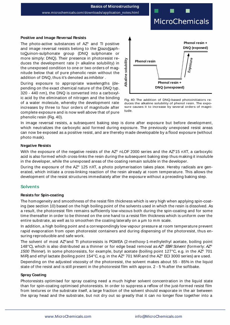
Positive and Image Reversal ResistsThe photo-active substances of AZ® and TI positive and image reversal resists belong to the DiazoNaph-toQuinon-sulphonate group (DNQ sulphonate or more simply: DNQ). Their presence in photoresist re-duces the development rate (= alkaline solubility) in the unexposed condition to one or two orders of mag-nitude below that of pure phenolic resin without the addition of DNQ, thus it’s denoted as inhibitor .During exposure to appropriate wavelengths (de-pending on the exact chemical nature of the DNQ typ. 320 - 440 nm), the DNQ is converted into a carboxyl-ic acid by the elimination of nitrogen and the binding of a water molecule, whereby the development rate increases by three to four orders of magnitude after complete exposure and is now well above that of pure phenolic resin (Fig. 40).In image reversal resists, a subsequent baking step is done after exposure but before development, which neutralizes the carboxylic acid formed during exposure. The previously unexposed resist areas can now be exposed as a positive resist, and are thereby made developable by a fl ood exposure (without photo mask).
Negative ResistsWith the exposure of the negative resists of the AZ® nLOF 2000 series and the AZ®15 nXT, a carboxylic acid is also formed which cross-links the resin during the subsequent baking step thus making it insoluble in the developer, while the unexposed areas of the coating remain soluble in the developer.During the exposure of the AZ® 125 nXT, a photo polymerisation takes place. Hereby radicals are gen-erated, which initiate a cross-linking reaction of the resin already at room temperature. This allows the development of the resist structures immediately after the exposure without a preceding baking step.
Solvents
Resists for Spin-coatingThe homogeneity and smoothness of the resist fi lm thickness which is very high when applying spin-coat-ing (see section 10) based on the high boiling point of the solvents used in which the resin is dissolved. As a result, the photoresist fi lm remains suffi ciently low-viscous both during the spin-coating and for some time thereafter in order to be thinned on the one hand to a resist fi lm thickness which is uniform over the entire substrate, as well as to smoothen the coating laterally on a µm to mm scale.In addition, a high boiling point and a correspondingly low vapour pressure at room temperature prevent rapid evaporation from open photoresist containers and during dispensing of the photoresist, thus en-suring reproducible and safe work.The solvent of most AZ®and TI photoresists is PGMEA (2-methoxy-1-methylethyl acetate, boiling point 148°C), which is also distributed as a thinner or for edge bead removal as AZ® EBR Solvent (formerly: AZ® 1500 Thinner). In some photoresists, for example, butyl acetate (boiling point 127°C, e.g. in the AZ® 701 MiR) and ethyl lactate (boiling point 154°C, e.g. in the AZ® 701 MiR and the AZ® ECI 3000 series) are used.Depending on the adjusted viscosity of the photoresist, the solvent makes about 55 - 85% in the liquid state of the resist and is still present in the photoresist fi lm with approx. 2 - 5 % after the softbake.
Spray CoatingPhotoresists optimised for spray coating need a much higher solvent concentration in the liquid state than for spin-coating optimised photoresists. In order to suppress a refl ow of the just-formed resist fi lm from textures or the substrate itself, a large fraction of the solvent should evaporate in the air between the spray head and the substrate, but not dry out so greatly that it can no longer fl ow together into a
Phenol resin
Phenol resin + DNQ (unexposed)
Phenol resin + DNQ (exposed)
Fig. 40: The addition of DNQ-based photoinitiators re-duces the alkaline solubility of phenol resin. The expo-sure causes it to increase by several orders of magni-tude.
Chapter01 MicroChemicals® – Fundamentals of Microstructuring
www.MicroChemicals.com [email protected]
Basics of Microstructuringwww.microchemicals.com/downloads/application_notes.html
closed photoresist fi lm.Therefore spray resists also contain low-boiling solvents such as acetone or MEK in addition to a high-boil-ing solvent such as PGMEA. The concentration ratio of high-boiling and low-boiling solvents determines whether the photoresist fi lm formed has either a maximum edge coverage (the rapidly evaporating sol-vent dominates) or a particularly smooth surface (high concentration of slowly evaporating solvents).
Dip Coating ResistsFor the dip coating optimised photoresists require a relatively high concentration of solvents in the liquid state to form a suffi ciently thin resist fi lm. In order to avoid run-off of the resist fi lm from the sub-strates usually held vertically in the dip, a large part of the solvent has to evaporate quickly after the resist coating. At the same time, however, the photoresist fi lm formed should remain suffi ciently low-viscous for several minutes to smoothen.Therefore dip coating photoresists also consist of a low boiling solvent such as acetone or MEK, to set the initial viscosity and thus the resist fi lm thickness, as well as a high-boiling solvent such as PGMEA for the homogenisation and smoothing the resist fi lm.
Other Components:In addition to the resin, photo-active substances and solvents, AZ® and TI photoresists can also contain anti-oxidising agents, adhesion promoters and substances for modifying the surface tension for the rapid smoothing of applied resist fi lms.Some resist such as Pl 177 oder der AZ® 520D are dyed for a simpler visual inspection of the homogeneity of the coating result with a dye absorbent in the visible spectral range.Image reversal resists contain additives which render the exposed photoresist areas insoluble in the de-veloper during the reversal process.
Thermal Resistance
Softening and RoundingNon-cross-linked resins have no defi ned melting point, but show a viscosity decreasing with increasing temperature. As a result, developed positive photoresist structures begin so strongly to soften in cer-tain temperature ranges that they are rounded from the formerly rectangular photoresist profi les to lens-shaped cross-sections (Refl ow), although the attachment points of the photoresist structures on the substrate are usually retained.This softening temperature which is necessary for a pronounced refl ow is between 100-110°C (AZ®1500, 4500, 4999, 9200, 40 XT, ECI 3000, PL 177) and 130-135°C (AZ® 701 MiR, TI 35ESX) with AZ® and TI positive and image reversal resists.Cross-linked resist structures like negative resists or thermally cross-linked positive resists show no thermoplastic behaviour and thus no refl ow even at higher temperatures. In the case of positive resists, cross-linking by means of deep-UV hardening (section 19.3 on page 98), which is carried out only on the surface, can prevent thermal rounding.
EmbrittlementFrom about 130°C on, photoresist fi lms, accompanied by an increasingly brownish colouring, in-creasingly react with (air) oxygen and become embrittled, which increases the risk of cracking when mechanical stresses occur. These cracks are mostly visible only under the microscope, but can lead to defects even in wet-chemical processes such as etching or the electroplating if the cracks bridge the entire resist thickness between the substrate and the medium over the resist fi lm.The hotter the baking is, and the thicker (and hence more sensitive to cracking) the resist fi lm is, the gen-tler the cooling rate should be and the more careful the further handling of the substrates.
Thermal Cross-linkingNon-cross-linked positive resist structures begin to thermally cross-link from about 130°C. During their processing, cross-linked negative resist structures increase their degree of cross-linking towards higher
Chapter01 MicroChemicals® – Fundamentals of Microstructuring
www.MicroChemicals.com [email protected]
Basics of Microstructuringwww.microchemicals.com/downloads/application_notes.html
temperatures.As a result, the chemical stability of the resist structure can be increased, but for this reason the subse-quent desired wet-chemical removal of the resist can become diffi cult or even impossible.
ShrinkageAs the temperature increases, not only does the residual solvent content of the resist further decrease, but also volatile components of the resin evaporate. As a consequence, resist structures shrink, so that a slight softening or deformation can be observed also in cross-linked resins of negative resists (the AZ® 125 nXT shows this behaviour comparatively clearly) without a rounding having occurred from reaching a softening temperature.
Chemical Resistance
AcidsIn most aqueous acid media as well as more concentrated hydrochloric, phosphorus, sulphuric or hy-drofl uoric acid, AZ ® and TI resists are suffi ciently stable enough for typical etching processes or electro plating.Strongly oxidizing acids such as nitric acid or mixtures of hydrogen peroxide and sulphuric acid chemical-ly attack the photoresist and in the case of hydrofl uoric acid, the diff usion of the F- ions to the substrate and its etching attack can lead to premature peeling of the resist layer.
BasesThe alkaline stability of AZ® and TI resists is signifi cantly lower than that in acids. Exposed positive resists and unexposed AZ® negative resists are already developed with, for example, 0.5% NaOH or KOH, unex-posed positive resist start to dissolve from pH values of approx. 9 - 10.A cross-linking of the resin (thermal cross-linking of positive resists by means of a hardbake at tempera-tures > 140°C or using cross-linked negative resists) signifi cantly increases the alkaline stability. However, even highly cross-linked photoresist structures are not suitable under any circumstances as masks for KOH or TMAH-based silicon etching. For this purpose, a hard mask of SiO2, silicon nitride or alkaline-sta-ble and well adhering metals such as chromium should be used here, patterned via photolithography.
Organic SolventsAZ® and TI positive and image reversal resists are soluble in most organic solvents. Increased but not per-manent stability against solvents is attainable via cross-linking via deep UV curing, a suffi cient hardbake, or the use of cross-linking negative resists such as the AZ® nLOF 2000 series.
Plating SolutionsIf proper processed, our photoresists are suffi ciently stable in all common acidic electrolytes, while al-kaline electrolytes attack the resist structures and can thus organically contaminate the bath. The use of cross-linked negative resists, such as the AZ® 15 nXT or 125 nXT, can also allow for the use of resist masks in moderately alkaline electrolytes.
Dry Etching Stability
Chemical and Physical StabilityThe stability of resins and polymers in plasmas depends on their basic chemical structure and is there-fore comparable with all phenolic resin-based AZ® and TI resists. A residual solvent concentration which is as minimal as possible, like that attained by means of a suffi cient softbake, can further stabilise the resist structures.The more oxygen is present in the plasma, the higher the removal rate of the resist structures, which can be used during the desired transfer of the resist profi le into the underlying substrate.
Chapter01 MicroChemicals® – Fundamentals of Microstructuring
www.MicroChemicals.com [email protected]
Basics of Microstructuringwww.microchemicals.com/downloads/application_notes.html
Thermal StabilityOne main criterion in the selection of the suitable resists for the dry etching is often a high softening temperature to prevent a thermal rounding of the mask during etch-ing. Because the softening temperature of most positive resists is in the vicinity of 100-110°C and their processing can only increase this temperature range to a certain extent, measures to reduce the temperatures oc-curring in the dry etching or the use of nega-tive resists are usually more eff ective.
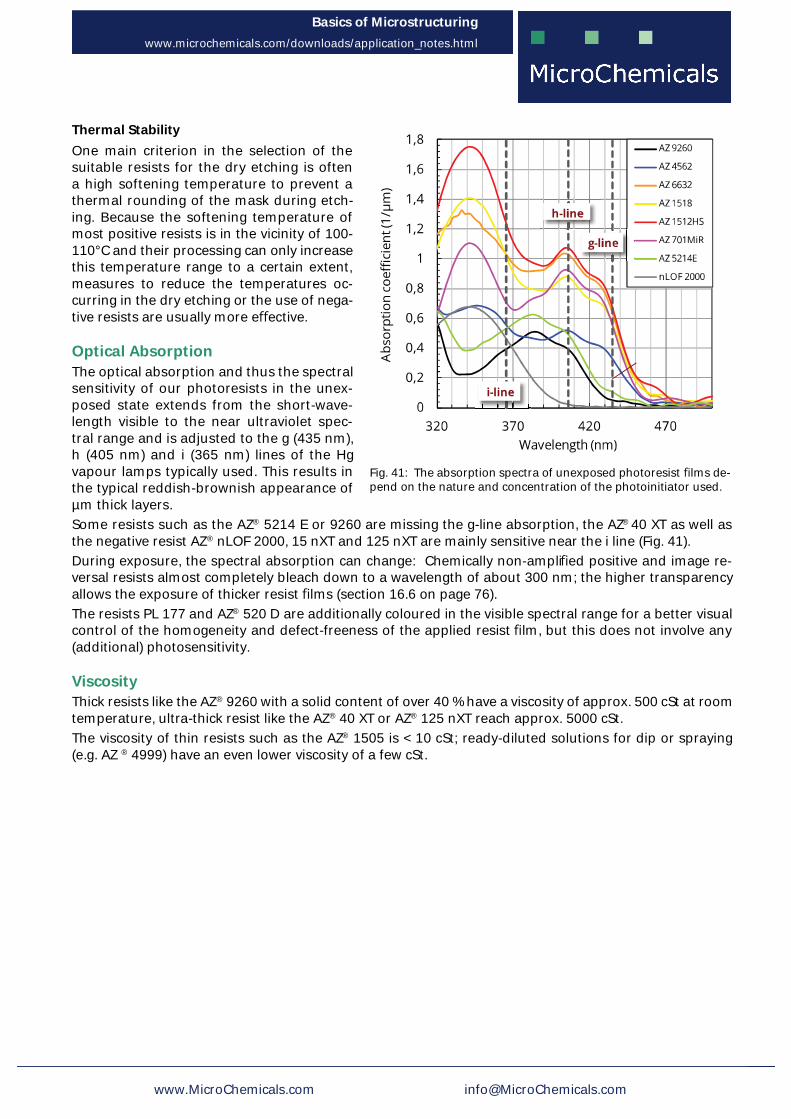
Optical AbsorptionThe optical absorption and thus the spectral sensitivity of our photoresists in the unex-posed state extends from the short-wave-length visible to the near ultraviolet spec-tral range and is adjusted to the g (435 nm), h (405 nm) and i (365 nm) lines of the Hg vapour lamps typically used. This results in the typical reddish-brownish appearance of µm thick layers.Some resists such as the AZ® 5214 E or 9260 are missing the g-line absorption, the AZ® 40 XT as well as the negative resist AZ® nLOF 2000, 15 nXT and 125 nXT are mainly sensitive near the i line (Fig. 41).During exposure, the spectral absorption can change: Chemically non-amplifi ed positive and image re-versal resists almost completely bleach down to a wavelength of about 300 nm; the higher transparency allows the exposure of thicker resist fi lms (section 16.6 on page 76).The resists PL 177 and AZ® 520 D are additionally coloured in the visible spectral range for a better visual control of the homogeneity and defect-freeness of the applied resist fi lm, but this does not involve any (additional) photosensitivity.
ViscosityThick resists like the AZ® 9260 with a solid content of over 40 % have a viscosity of approx. 500 cSt at room temperature, ultra-thick resist like the AZ® 40 XT or AZ® 125 nXT reach approx. 5000 cSt.The viscosity of thin resists such as the AZ® 1505 is < 10 cSt; ready-diluted solutions for dip or spraying (e.g. AZ ® 4999) have an even lower viscosity of a few cSt.
Fig. 41: The absorption spectra of unexposed photoresist fi lms de-pend on the nature and concentration of the photoinitiator used.

Our Photoresists: Application Areas and Compatibilities
Recommended Applications 1 Resist Family Photoresists Resist Film Thickness 2 Recommended Developers 3 Recommended Re-
movers 4
1 In g
ener
al, a
lmos
t all
resi
sts
can
be u
sed
for a
lmos
t any
app
licat
ion.
How
ever
, the
spe
cial
pro
perti
es o
f eac
h re
sist
fam
ily
mak
es th
em s
peci
ally
sui
ted
for c
erta
in fi
elds
of a
pplic
atio
n.
2 Res
ist f
ilm th
ickn
ess
achi
evab
le a
nd p
roce
ssab
le w
ith s
tand
ard
equi
pmen
t und
er s
tand
ard
cond
ition
s. S
ome
resi
sts
can
be d
ilute
d fo
r low
er fi
lm th
ickn
esse
s; w
ith a
dditi
onal
effo
rt al
so th
icke
r res
ist f
ilms
can
be a
chie
ved
and
proc
esse
d.
3 Met
al io
n fre
e (M
IF) d
evel
oper
s ar
e si
gnifi
cant
ly m
ore
expe
nsiv
e, a
nd re
ason
able
if m
etal
ion
free
deve
lopm
ent i
s re
-qu
ired.
4 A
lso
depe
nds
on th
e re
sist
pro
cess
ing
and
subs
rrat
e m
ater
ials
use
d, d
etai
ls s
ee s
ectio
n ‘re
mov
ers’
nex
t pag
e
Posi
tive
Improved adhesion for wet etching, no focus on steep resist sidewalls
AZ® 1500
AZ® 1505 AZ® 1512 HS AZ® 1514 H AZ® 1518
≈ 0.5 µm ≈ 1.0 - 1.5 µm ≈ 1.2 - 2.0 µm ≈ 1.5 - 2.5 µm
AZ® 351B, AZ® 326 MIF, AZ® 726 MIF, AZ® Developer
AZ® 100 Remover, TechniStrip® P1316 TechniStrip® P1331
AZ® 4500 AZ® 4533 AZ® 4562
≈ 3 - 5 µm ≈ 5 - 10 µm AZ® 400K, AZ® 326 MIF, AZ® 726 MIF, AZ® 826 MIF
AZ® P4000
AZ® P4110 AZ® P4330 AZ® P4620 AZ® P4903
≈ 1 - 2 µm ≈ 3 - 5 µm
≈ 6 - 20 µm ≈ 10 - 30 µm
AZ® 400K, AZ® 326 MIF, AZ® 726 MIF, AZ® 826 MIF
AZ® PL 177 AZ® PL 177 ≈ 3 - 8 µm AZ® 351B, AZ® 400K, AZ® 326 MIF, AZ® 726 MIF, AZ® 826 MIF Spray coating AZ® 4999 ≈ 1 - 15 µm AZ® 400K, AZ® 326 MIF, AZ® 726 MIF, AZ® 826 MIF Dip coating MC Dip Coating Resist ≈ 2 - 15 µm AZ® 351B, AZ® 400K, AZ® 326 MIF, AZ® 726 MIF, AZ® 826 MIF
Steep resist sidewalls, high resolution and aspect ratio for e. g. dry etching or plating
AZ® ECI 3000 AZ® ECI 3007 AZ® ECI 3012 AZ® ECI 3027
≈ 0.7 µm ≈ 1.0 - 1.5 µm
≈ 2 - 4 µm AZ® 351B, AZ® 326 MIF, AZ® 726 MIF, AZ® Developer
AZ® 9200 AZ® 9245 AZ® 9260
≈ 3 - 6 µm ≈ 5 - 20 µm AZ® 400K, AZ® 326 MIF, AZ® 726 MIF
Elevated thermal softening point and high resolution for e. g. dry etching AZ® 701 MiR AZ® 701 MiR (14 cPs)
AZ® 701 MiR (29 cPs) ≈ 0.8 µm
≈ 2 - 3 µm AZ® 351B, AZ® 326 MIF, AZ® 726 MIF, AZ® Developer
Posi
tive
(che
m.
ampl
ified
)
Steep resist sidewalls, high resolution and aspect ratio for e. g. dry etching or plating
AZ® XT AZ® 12 XT-20PL-05 AZ® 12 XT-20PL-10 AZ® 12 XT-20PL-20 AZ® 40 XT
≈ 3 - 5 µm ≈ 6 - 10 µm
≈ 10 - 30 µm ≈ 15 - 50 µm
AZ® 400K, AZ® 326 MIF, AZ® 726 MIF AZ® 100 Remover, TechniStrip® P1316 TechniStrip® P1331
AZ® IPS 6050 ≈ 20 - 100 µm
Imag
e Re
-ve
rsal
Elevated thermal softening point and undercut for lift-off applications
AZ® 5200 AZ® 5209 AZ® 5214
≈ 1 µm ≈ 1 - 2 µm
AZ® 351B, AZ® 326 MIF, AZ® 726 MIF TechniStrip® Micro D2 TechniStrip® P1316 TechniStrip® P1331 TI TI 35ESX
TI xLift-X ≈ 3 - 4 µm ≈ 4 - 8 µm
Nega
tive
(Cro
ss-li
nkin
g)
Negative resist sidewalls in combination with no thermal softening for lift-off application
AZ® nLOF 2000 AZ® nLOF 2020 AZ® nLOF 2035 AZ® nLOF 2070
≈ 1.5 - 3 µm ≈ 3 - 5 µm
≈ 6 - 15 µm AZ® 326 MIF, AZ® 726 MIF, AZ® 826 MIF TechniStrip® NI555 TechniStrip® NF52 TechniStrip® MLO 07
AZ® nLOF 5500 AZ® nLOF 5510 ≈ 0.7 - 1.5 µm
Improved adhesion, steep resist side-walls and high aspect ratios for e. g. dry etching or plating
AZ® nXT
AZ® 15 nXT (115 cPs) AZ® 15 nXT (450 cPs)
≈ 2 - 3 µm ≈ 5 - 20 µm AZ® 326 MIF, AZ® 726 MIF, AZ® 826 MIF
AZ® 125 nXT ≈ 20 - 100 µm AZ® 326 MIF, AZ® 726 MIF, AZ® 826 MIF TechniStrip® P1316 TechniStrip® P1331 TechniStrip® NF52 TechniStrip® MLO 07
Our Developers: Application Areas and Compatibilities Inorganic Developers (typical demand under standard conditions approx. 20 L developer per L photoresist) AZ® Developer is based on sodium phosphate and –metasilicate, is optimized for minimal aluminum attack and is typically used diluted 1 : 1 in DI water for high contrast or undiluted for high development rates. The dark erosion of this developer is slightly higher compared to other developers. AZ® 351B is based on buffered NaOH and typically used diluted 1 : 4 with water, for thick resists up to 1 : 3 if a lower contrast can be tolerated. AZ® 400K is based on buffered KOH and typically used diluted 1 : 4 with water, for thick resists up to 1 : 3 if a lower contrast can be tolerated. AZ® 303 specifically for the AZ® 111 XFS photoresist based on KOH / NaOH is typically diluted 1 : 3 - 1 : 7 with water, depending on whether a high development rate, or a high contrast is required
Metal Ion Free (TMAH-based) Developers (typical demand under standard conditions approx. 5 - 10 L developer concentrate per L photoresist) AZ® 326 MIF is 2.38 % TMAH- (TetraMethylAmmoniumHydroxide) in water.

AZ® 726 MIF is 2.38 % TMAH- (TetraMethylAmmoniumHydroxide) in water, with additional surfactants for rapid and uniform wetting of the substrate (e. g. for puddle development) AZ® 826 MIF is 2.38 % TMAH- (TetraMethylAmmoniumHydroxide) in water, with additional surfactants for rapid and uniform wetting of the substrate (e. g. for puddle development) and other additives for the removal of poorly solu-ble resist components (residues with specific resist families), however at the expense of a slightly higher dark erosion.
Our Removers: Application Areas and Compatibilities AZ® 100 Remover is an amine solvent mixture and standard remover for AZ® and TI photoresists. To improve its performance, AZ® 100 remover can be heated to 60 - 80°C. Because the AZ ® 100 Remover reacts highly alkaline with water, it is suitable for this with respect to sensitive substrate materials such as Cu, Al or ITO only if contamination with water can be ruled out.. TechniStrip® P1316 is a remover with very strong stripping power for Novolak-based resists (including all AZ® positive resists), epoxy-based coatings, polyimides and dry films. At typical application temperatures around 75°C, TechniStrip® P1316 may dissolve cross-linked resists without residue also, e.g. through dry etching or ion implantation. TechniStrip® P1316 can also be used in spraying processes. For alkaline sensitive materials, TechniStrip® P1331 would be an alternative to the P1316. Nicht kompatibel mit Au oder GaAs. TechniStrip® P1331 can be an alternative for TechniStrip® P1316 in case of alkaline sensitive materials. TechniStrip® P1331 is not compatible with Au or GaAs. TechniStrip® NI555 is a stripper with very strong dissolving power for Novolak-based negative resists such as the AZ® 15 nXT and AZ® nLOF 2000 series and very thick positive resists such as the AZ® 40 XT. TechniStrip® NI555 was developed not only to peel cross-linked resists, but also to dissolve them without residues. This prevents contamination of the basin and filter by resist particles and skins, as can occur with standard strippers. TechniStrip ® NI555 is not compatible with Au or GaAs. TechniClean™ CA25 is a semi-aqueous proprietary blend formulated to address post etch residue (PER) removal for all interconnect and technology nodes. Extremely efficient at quickly and selectively removing organo-metal oxides from Al, Cu, Ti, TiN, W and Ni. TechniStrip™ NF52 is a highly effective remover for negative resists (liquid resists as well as dry films). The intrinsic nature of the additives and solvent make the blend totally compatible with metals used throughout the BEOL interconnects to WLP bumping applications. TechniStrip™ Micro D2 is a versatile stripper dedicated to address resin lift-off and dissolution on negative and positive tone resist. The organic mixture blend has the particularity to offer high metal and material compatibility allowing to be used on all stacks and particularly on fragile III/V substrates for instance. TechniStrip™ MLO 07 is a highly efficient positive and negative tone photoresist remover used for IR, III/V, MEMS, Photonic, TSV mask, solder bumping and hard disk stripping applications. Developed to address high dissolution performance and high material compatibility on Cu, Al, Sn/Ag, Alumina and common organic substrates.
Our Wafers and their Specifications Silicon-, Quartz-, Fused Silica and Glass Wafers Silicon wafers are either produced via the Czochralski- (CZ-) or Float zone- (FZ-) method. The more expensive FZ wafers are primarily reasonable if very high-ohmic wafers (> 100 Ohm cm) are required. Quartz wafers are made of monocrystalline SiO2, main criterion is the crystal orientation (e. g. X-, Y-, Z-, AT- or ST-cut) Fused silica wafers consist of amorphous SiO2. The so-called JGS2 wafers have a high transmission in the range of ≈ 280 - 2000 nm wavelength, the more expensive JGS1 wafers at ≈ 220 - 1100 nm. Our glass wafers, if not otherwise specified, are made of borosilicate glass. Specifications Common parameters for all wafers are diameter, thickness and surface (1- or 2-side polished). Fused silica wafers are made either of JGS1 or JGS2 material, for quartz wafers the crystal orientation needs to be defined. For silicon wafers, beside the crystal orientation (<100> or <111>) the doping (n- or p-type) as well as the resistivity (Ohm cm) are selection criteria. Prime- ,Test-, and Dummy Wafers Silicon wafers usually come as „Prime-grade“ or „Test-grade“, latter mainly have a slightly broader particle specification. „Dummy-Wafers“ neither fulfill Prime- nor Test-grade for different possible reasons (e. g. very broad or missing specification of one or several parameters, reclaim wafers, no particle specification) but might be a cheap alternative for e. g. resist coating tests or equipment start-up. Our Silicon-, Quartz-, Fused Silica and Glass Wafers Our frequently updated wafer stock list can be found here: è www.microchemicals.com/products/wafers/waferlist.html
Further Products from our Portfolio Plating Plating solutions for e. g. gold, copper, nickel, tin or palladium: è www.microchemicals.com/products/electroplating.html Solvents (MOS, VLSI, ULSI) Acetone, isopropyl alcohol, MEK, DMSO, cyclopentanone, butylacetate, ... è www.microchemicals.com/products/solvents.html Acids and Bases (MOS, VLSI, ULSI) Hydrochloric acid, sulphuric acid, nitric acid, KOH, TMAH, … è www.microchemicals.com/products/etchants.html Etching Mixtures for e. g. chromium, gold, silicon, copper, titanium, ... è www.microchemicals.com/products/etching_mixtures.html
Further Information Technical Data Sheets: www.microchemicals.com/downloads/product_data_sheets/photoresists.html Material Safety Data Sheets (MSDS): www.microchemicals.com/downloads/safety_data_sheets/msds_links.html
Our Photolithography Book and -Posters
We see it as our main task to make you understand all aspects of microstructuring in an application-oriented way. At present, we have implemented this claim with our book Photolithography on over 200 pages, as well as attractively designed DIN A0 posters for your office or laboratory. We will gladly send both of these to you free of charge as our customer (if applicable, we charge shipping costs for non-European deliveries): www.microchemicals.com/downloads/brochures.html www.microchemicals.com/downloads/posters.html Thank you for your interest!
Disclaimer of Warranty & Trademarks All information, process descriptions, recipes, etc. contained in this book are compiled to the best of our knowledge. Nevertheless, we can not guarantee the correctness of the information. Particularly with regard to the formulations for chemical (etching) processes we assume no guarantee for the correct specification of the components, the mixing conditions, the preparation of the batches and their application. The safe sequence of mixing components of a recipe usually does not correspond to the order of their listing. We do not warrant the full disclosure of any indications (among other things, health, work safety) of the risks associated with the preparation and use of the recipes and processes. The information in this book is based on our current knowledge and experience. Due to the abundance of possible influences in the processing and application of our products, they do not exempt the user from their own tests and trials. A guarantee of certain properties or suitability for a specific application can not be derived from our data. As a matter of principle, each employee is required to provide sufficient information in advance in the appropriate cases in order to prevent damage to persons and equipment. All descriptions, illustrations, data, conditions, weights, etc. can be changed without prior notice and do not constitute a contractually agreed product characteristics. The user of our products is responsible for any proprietary rights and existing laws. Merck, Merck Performance Materials, AZ, the AZ logo, and the vibrant M are trademarks of Merck KGaA, Darmstadt, Germany MicroChemicals GmbH Fon: +49 (0)731 977 343 0 Nicolaus-Otto-Str. 39 Fax: +49 (0)731 977 343 29 89079, Ulm e-Mail: [email protected] Germany Internet: www.microchemicals.net