COMPOSITE DENDRIMER MATERIALS - MINT Center · Center for Materials for Information Technology an...
20
Center for Materials for Information Technology an NSF Materials Science and Engineering Center COMPOSITE DENDRIMER MATERIALS Shane Street (UA, Chemistry) Mark Weaver (UA, MtE) John Barnard (Pitt, Mat. Sci.) [email protected]
Transcript of COMPOSITE DENDRIMER MATERIALS - MINT Center · Center for Materials for Information Technology an...
Center for Materials for Information Technologyan NSF Materials Science and Engineering Center
COMPOSITE DENDRIMER MATERIALS
Shane Street (UA, Chemistry)Mark Weaver (UA, MtE)
John Barnard (Pitt, Mat. Sci.)[email protected]

Center for Materials for Information Technologyan NSF Materials Science and Engineering Center
Areas of Research
� Dendrimer-mediated Ultrathin Films� Dendrimer-mediated overlayer film growth; morphology� Nanomechanical behavior of metal/dendrimer composites� Adhesion and hardness issues
� Dendrimer-mediated Synthesis of Nanoparticles and Patterned Nanostructures� Microcontact printing� Metal/dendrimer composite structures� Metallic nanoparticles

Center for Materials for Information Technologyan NSF Materials Science and Engineering Center
Dendrimers as Functional ComponentsStarburst PAMAM Dendrimers
Repeated UnitsN- (CH2)2 -N
(CH2)2 - CO -NH - (CH2)2-N
(CH2)2 - CO -NH - (CH2)2-NCore
Dendrimers are 3d, highly branched, macromoleculeswith a core/repeat unit/terminal shell structure.
Generally classified by generation, e.g., G4: -NH2 terminated64 endgroupsMW ~ 14000
Center for Materials for Information Technologyan NSF Materials Science and Engineering Center
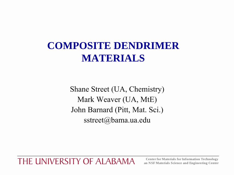
Dendrimer Adlayers and Interfacial Interactions
~3-2
0 nm
Typical Samples Schematic
Center for Materials for Information Technologyan NSF Materials Science and Engineering Center
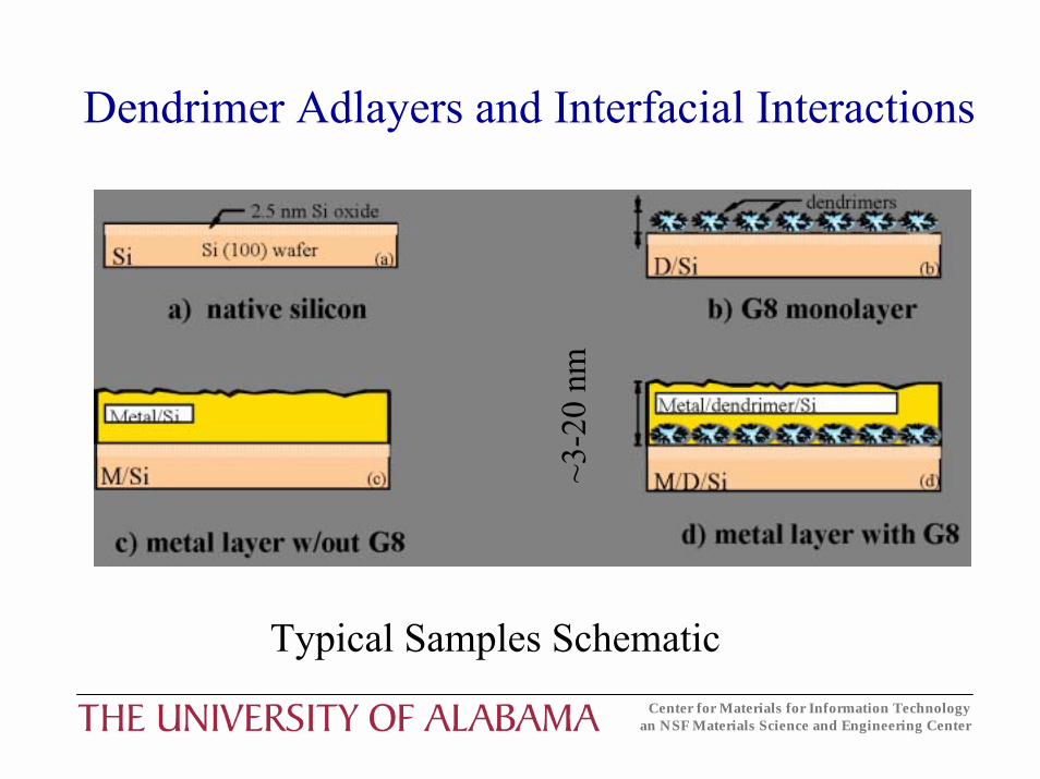
Dendrimer-Mediated Film Morphology10 nm Co 10 nm Cr 10 nm Au 10 nm Cu1 µm x 1 µm
scan size
Bare Si
G8

Center for Materials for Information Technologyan NSF Materials Science and Engineering Center
Dendrimer-mediated Overlayer Film Growth
� Increase in squareness� Decrease in magnetic
moment� Influence is on ordering in
overlayer Co?
Influence of morphology of the Cu seed layer on magneticproperties of an overlayer (Co)

Center for Materials for Information Technologyan NSF Materials Science and Engineering Center
Molecular Interlayers and Abrasive Wear�AFM image of residual impressionleft by diamond scratch tip
�Impression made in thick Cu film
�Blunted Berkovitch shape
�Scratches carried out in face-forward mode
�Velocity: 1 micron/second
Si
15 nm Cu
SiN N
N
N
N
N
N
N N
N
N
NN
N
NN
N
N
N
N
N
NNN
N
N
N
N
NN
NN N N NN N
N
NN
NN
NN
NN
NNNNNN
NN
NN
NN
NN
NN
XX
XXXX XX X X XX
XX
XX
XX
XX
XX
XX
XX
XX
XX
XX
XX
X XXXXXXXXXXX
XXXX
XX
XXX
X
XX
XXX
X
XX
N N
N
N
N
N
N
N N
N
N
NN
N
NN
N
N
N
N
N
NNN
N
N
N
N
NN
NN N N NN N
N
NN
NN
NN
NN
NNNNNN
NN
NN
NN
NN
NN
XX
XXXX XX X X XX
XX
XX
XX
XX
XX
XX
XX
XX
XX
XX
XX
X XXXXXXXXXXX
XXXX
XX
XXX
X
XX
XXX
X
XX
N N
N
N
N
N
N
N N
N
N
NN
N
NN
N
N
N
N
N
NNN
N
N
N
N
NN
NN N N NN N
N
NN
NN
NN
NN
NNNNNN
NN
NN
NN
NN
NN
XX
XXXX XX X X XX
XX
XX
XX
XX
XX
XX
XX
XX
XX
XX
XX
X XXXXXXXXXXX
XXXX
XX
XXX
X
XX
XXX
X
XX
15 nm Cuvs
Constant load (4 mN) nanoscratches, 100 µm long.

Center for Materials for Information Technologyan NSF Materials Science and Engineering Center
SEM Images of Nanoscratch Events4 mN constant load, Berkovitch tip (face forward)
15 nm Cu/Si 15 nm Cu/G8/Si
Plowing Irregular cutting
Center for Materials for Information Technologyan NSF Materials Science and Engineering Center
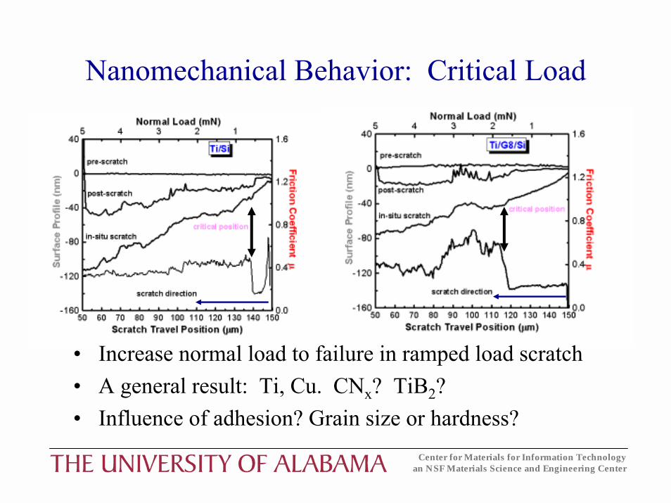
Nanomechanical Behavior: Critical Load
� Increase normal load to failure in ramped load scratch� A general result: Ti, Cu. CNx? TiB2?� Influence of adhesion? Grain size or hardness?

Center for Materials for Information Technologyan NSF Materials Science and Engineering Center
Dendrimer Adlayers and Interfacial Interactions
� The presence of the dendrimer monolayer influences the morphology, nanomechanical properties and chemical composition of overlayer metal ultrathin films (growth modes, grain size, chemical composition of the interface, resistivity of the thin film)
� Improve overlayer magnetic materials properties (Grain size control?)
� Distinguish between hardness, and adhesion effects in nanomechanical properties? Does adlayer improve “hard coatings” adhesion or fracture resistance?
Center for Materials for Information Technologyan NSF Materials Science and Engineering Center
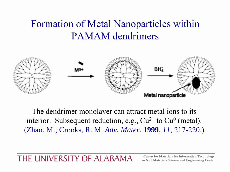
Formation of Metal Nanoparticles within PAMAM dendrimers
The dendrimer monolayer can attract metal ions to its interior. Subsequent reduction, e.g., Cu2+ to Cu0 (metal).
(Zhao, M.; Crooks, R. M. Adv. Mater. 1999, 11, 217-220.)
Center for Materials for Information Technologyan NSF Materials Science and Engineering Center
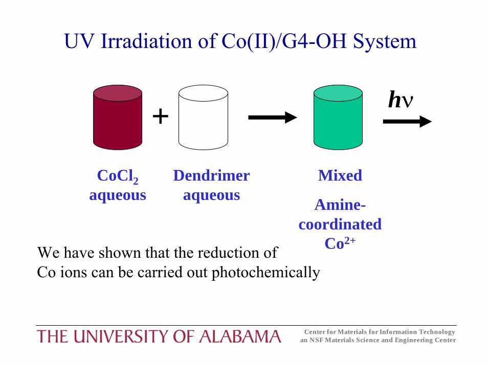
UV Irradiation of Co(II)/G4-OH System
hν+
CoCl2aqueous
Dendrimer aqueous
Mixed
Amine-coordinated
Co2+We have shown that the reduction ofCo ions can be carried out photochemically

Center for Materials for Information Technologyan NSF Materials Science and Engineering Center
TEM image of Acicular Co Nanoparticles
The resulting particlesare acicular, metallic,and magnetic
Dr. M. Shamsuzzoha

Center for Materials for Information Technologyan NSF Materials Science and Engineering Center
Acicular Co Nanoparticles
-5000 -4000 -3000 -2000 -1000 0 1000 2000 3000 4000 5000-1.0x10⁻⁵
-5.0x10⁻⁶
0.0
5.0x10⁻⁶
1.0x10⁻⁵
HC = 300.6Oe
M (e
mu)
H (Oe)
Magnetic Hysteresis Loop of Co Nanoparticles
The Co particles produced are relatively monodisperse, acicular, magnetic, and apparently metallic.
(0001)hcp Co with stacking faults
TEM Image of Single Co Nanoparticle
Zhang et al. manuscript in preparation

Center for Materials for Information Technologyan NSF Materials Science and Engineering Center
Patterning Surfaces Using Microcontact Printing
� Microcontact printing (µCP) is a means of forming chemical patterns on surfaces.
� A polydimethylsiloxane (PDMS) stamp is used. The stamp is treated with the chemical �ink� which is subsequently transferred to the substrate.
Preparation of stamp
Inking of stamp
Contact withsubstrate
Patterned ink remains

Center for Materials for Information Technologyan NSF Materials Science and Engineering Center
Dendrimer Multilayer PatterningAFM Image of Patterned G4 Dendrimer Multilayer
Unusually stable dendrimer multilayers can be patterned using microcontact printing techniques.
Arrington et al. Langmuir 18 (2002) 7788-7791
Center for Materials for Information Technologyan NSF Materials Science and Engineering Center
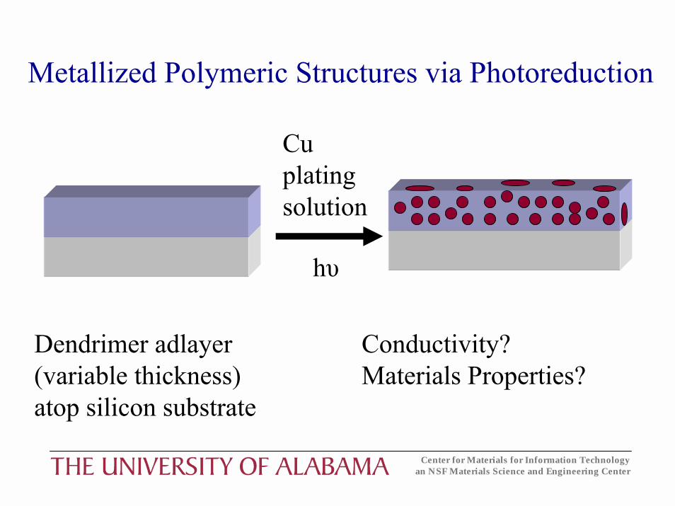
Metallized Polymeric Structures via Photoreduction
Cu plating solution
hυ
Dendrimer adlayer(variable thickness)atop silicon substrate
Conductivity? Materials Properties?

Center for Materials for Information Technologyan NSF Materials Science and Engineering Center
Metallized Polymeric Structures via Photoreduction
� G4.5 monolayer in CuSO4 plating solution
� Copper appears to be metallic rather than Cu2+
� Increase in metal content as a function of irradiation time
Cu 2p XPS: G4.5/Cu(plating solution)
Center for Materials for Information Technologyan NSF Materials Science and Engineering Center
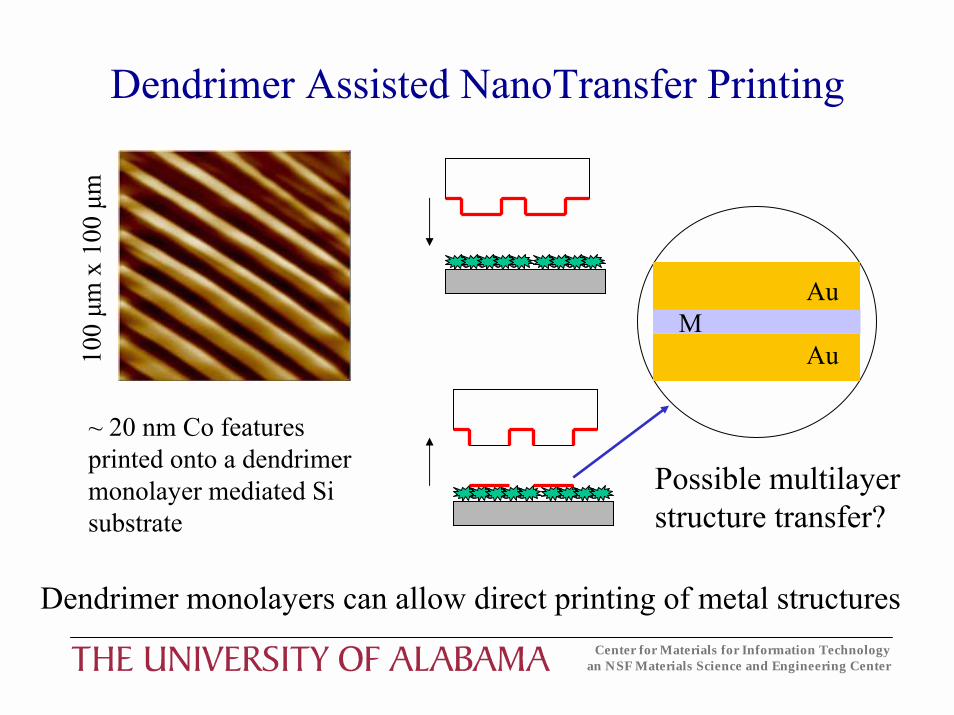
Dendrimer Assisted NanoTransfer Printing10
0 µm
x 1
00 µ
m
~ 20 nm Co features printed onto a dendrimer monolayer mediated Sisubstrate
Au
AuM
Possible multilayerstructure transfer?
Dendrimer monolayers can allow direct printing of metal structures
Center for Materials for Information Technologyan NSF Materials Science and Engineering Center
Dendrimer Patterning and Functional Nanostructures
� Dendrimer mono- and multilayers can be patterned by printing.� Metal ions can be reduced under UV irradiation in the presence
of the dendrimer. � Interdendrimer particles Co particles produced are relatively
monodisperse, acicular, magnetic, and apparently metallic.� Functional nanopatterned multilayer structures?� Shape, size selectivity in magnetic nanoparticles?