Compensated Semiconductors
21
A semiconductor is a material with conducting properties between those of a good insulator (e.g. glass) and a good conductor (e.g. copper). The most commonly used semiconductor is silicon.
-
Upload
mohammad-gulam-ahamad -
Category
Documents
-
view
228 -
download
0
Transcript of Compensated Semiconductors
7/27/2019 Compensated Semiconductors
http://slidepdf.com/reader/full/compensated-semiconductors 1/21
A semiconductor is a material with conductingproperties between those of a good insulator
(e.g. glass) and a good conductor (e.g. copper). The most commonly used semiconductor is
silicon.
7/27/2019 Compensated Semiconductors
http://slidepdf.com/reader/full/compensated-semiconductors 2/21
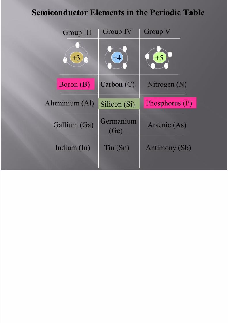
(Ge)
+3 +4 +5
Group III Group IV Group V
Boron (B) Carbon (C) Nitrogen (N)
Aluminium (Al) Silicon (Si) Phosphorus (P)
Gallium (Ga) Germanium Arsenic (As)
Indium (In) Tin (Sn) Antimony (Sb)
Semiconductor Elements in the Periodic Table
7/27/2019 Compensated Semiconductors
http://slidepdf.com/reader/full/compensated-semiconductors 3/21
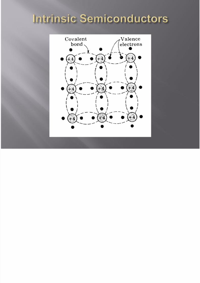
Each silicon atom has an outer shell with fourvalence electrons and four vacancies (It is atetravalent element).
In intrinsic (pure) silicon, atoms join togetherby forming covalent bonds. Each atom shares itsvalence electrons with each of four adjacentneighbours effectively filling its outer shell.
7/27/2019 Compensated Semiconductors
http://slidepdf.com/reader/full/compensated-semiconductors 4/21
7/27/2019 Compensated Semiconductors
http://slidepdf.com/reader/full/compensated-semiconductors 5/21
The structure has zero overall charge
The complete nature of the structure meansthat at absolute zero temperature (0 K) none of
the electrons is available for conduction…thusfar the material is an insulator.
7/27/2019 Compensated Semiconductors
http://slidepdf.com/reader/full/compensated-semiconductors 6/21
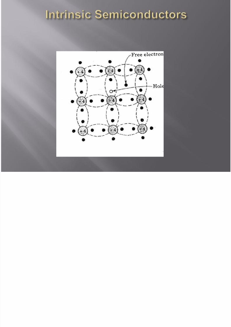
At room temperature some of the electronsare able to acquire sufficient thermal energyto break free from their bond.
Whenever an electron leaves its position inthe lattice it leaves a vacancy known as ahole.
The process is known as electron-hole pair generation
7/27/2019 Compensated Semiconductors
http://slidepdf.com/reader/full/compensated-semiconductors 7/21
7/27/2019 Compensated Semiconductors
http://slidepdf.com/reader/full/compensated-semiconductors 8/21
A freed electron can move through the body ofthe material until it encounters another brokenbond where it is drawn in to complete the bond
or recombines.
7/27/2019 Compensated Semiconductors
http://slidepdf.com/reader/full/compensated-semiconductors 9/21
At a given temperature there is a dynamicequilibrium between thermal electron-hole
generation and the recombination of electrons and
holes As a result the concentration of electrons and
holes in an intrinsic semiconductor is constant atany given temperature.
The higher the temperature the more electron-hole pairs that are present.
7/27/2019 Compensated Semiconductors
http://slidepdf.com/reader/full/compensated-semiconductors 10/21
Two mechanisms for conduction become possiblewhen a bond breaks:
1. Due to the movement of the freed electron.
2. Due to neighbouring electrons moving into thehole leaving a space behind it. (This can be mostsimply thought of as movement of the hole, asingle moving positive charge carrier even thoughit is actually a series of electrons that move.
7/27/2019 Compensated Semiconductors
http://slidepdf.com/reader/full/compensated-semiconductors 11/21
When an electric field (voltage) is applied, theholes move in one direction and the electrons inthe other.
However both current components are in thedirection of the field.
The conduction is ohmic, i.e. current isproportional to the applied voltage (field)
7/27/2019 Compensated Semiconductors
http://slidepdf.com/reader/full/compensated-semiconductors 12/21
The proportion of freed electrons is verysmall indeed:
In silicon the energy EG required to free anelectron is 1.2eV
The mean thermal energy (kT) is only25meV at room temperature (1/40 eV)
The proportion of freed electrons variesexponentially (-EG /kT), see handout.
7/27/2019 Compensated Semiconductors
http://slidepdf.com/reader/full/compensated-semiconductors 13/21
For an intrinsic semiconductor the number ofelectron and hole carriers, and thus theconductivity, increases rapidly with temperature.
This is not very useful. Hence we dope the material to produce an
extrinsic semiconductor.
7/27/2019 Compensated Semiconductors
http://slidepdf.com/reader/full/compensated-semiconductors 14/21
Instrinsic conduction is very small (see example).
Conductivity levels can be raised and controlledby doping with minute levels of impurity atoms to
give extrinsic or doped semiconductors. Extrinsic semiconductors may be further divided
into either n-type or p-type
7/27/2019 Compensated Semiconductors
http://slidepdf.com/reader/full/compensated-semiconductors 15/21
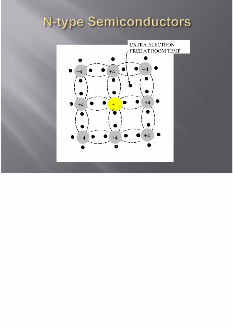
An n-type impurity atom has five outer(valence) electrons, rather than the four ofsilicon.
Only four of the outer electrons are requiredfor covalent bonding. The fifth is much moreeasily detached from the parent atom.
As the energy needed to free the fifth
electron is smaller than the thermal energyat room temperature virtually all are freed.
7/27/2019 Compensated Semiconductors
http://slidepdf.com/reader/full/compensated-semiconductors 16/21
+
5
+4
+4
+4
+4
EXTRA ELECTRON
FREE AT ROOM TEMP.
+4
+4
+4
+4
7/27/2019 Compensated Semiconductors
http://slidepdf.com/reader/full/compensated-semiconductors 17/21
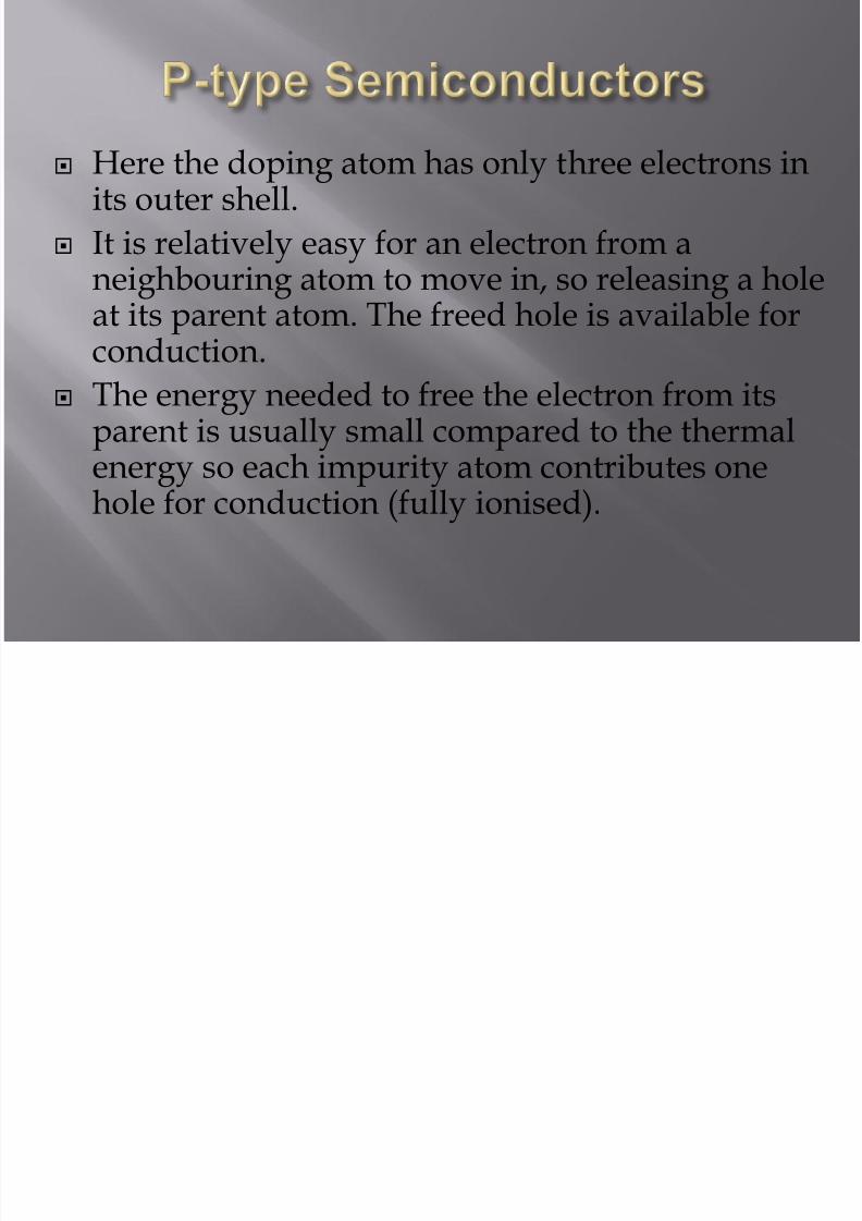
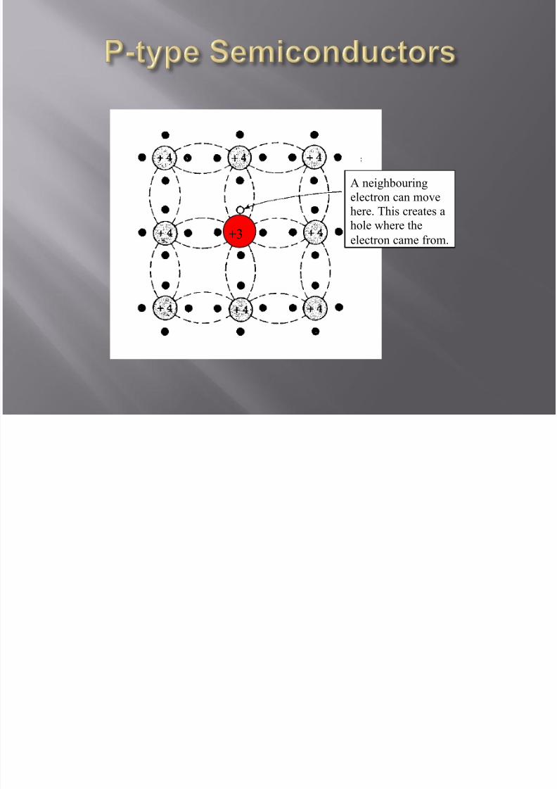
Here the doping atom has only three electrons inits outer shell.
It is relatively easy for an electron from aneighbouring atom to move in, so releasing a holeat its parent atom. The freed hole is available forconduction.
The energy needed to free the electron from itsparent is usually small compared to the thermalenergy so each impurity atom contributes onehole for conduction (fully ionised).
7/27/2019 Compensated Semiconductors
http://slidepdf.com/reader/full/compensated-semiconductors 18/21
A neighbouring
electron can movehere. This creates a
hole where the
electron came from.+3
7/27/2019 Compensated Semiconductors
http://slidepdf.com/reader/full/compensated-semiconductors 19/21
In both types of extrinsic semiconductor virtuallyall available charge carries are freed from theirparent atoms at room temperature. Temperature
variations thus make little difference to theconductivity .
For intrinsic conductivity the number of carriers,and thus , increases rapidly with temperature.
For both extrinsic and intrinsic mechanisms theconductivity is zero at T=0 K

7/27/2019 Compensated Semiconductors
http://slidepdf.com/reader/full/compensated-semiconductors 20/21
In an N-type semiconductor, conduction ismainly due to electrons (negative charges)
Positive charges (holes) are the minority
carriers.
7/27/2019 Compensated Semiconductors
http://slidepdf.com/reader/full/compensated-semiconductors 21/21
In a P-type semiconductor, conduction ismainly due to holes (positive charges)
Negative charges (electrons) are the minority
carriers.