Comparative Performance Analysis ... - Aircc Digital...
22
International Journal of VLSI design & Communication Systems (VLSICS) Vol.3, No.2, April 2012 DOI : 10.5121/vlsic.2012.3219 221 Comparative Performance Analysis of XOR- XNOR Function Based High-Speed CMOS Full Adder Circuits For Low Voltage VLSI Design Subodh Wairya 1 , Rajendra Kumar Nagaria 2 and Sudarshan Tiwari 2 1 Department of Electronics Engineering, Institute of Engineering & Technology (I.E.T), Lucknow, India, 226021 [email protected] 2 Department of ECED, Motilal Nehru National Institute of Technology (MNNIT), Allahabad, India, 211004 [email protected],[email protected] ABSTRACT This paper presents comparative study of high-speed, low-power and low voltage full adder circuits. Our approach is based on XOR-XNOR design full adder circuits in a single unit. A low power and high performance 9T full adder cell using a design style called “XOR (3T)” is discussed. The designed circuit commands a high degree of regularity and symmetric higher density than the conventional CMOS design style as well as it lowers power consumption by using XOR (3T) logic circuits. Gate Diffusion Input (GDI) technique of low-power digital combinatorial circuit design is also described. This technique helps in reducing the power consumption and the area of digital circuits while maintaining low complexity of logic design. This paper analyses, evaluates and compares the performance of various adder circuits. Several simulations conducted using different voltage supplies, load capacitors and temperature variation demonstrate the superiority of the XOR (3T) based full adder designs in term of delay, power and power delay product (PDP) compared to the other full adder circuits. Simulation results illustrate the superiority of the designed adder circuits against the conventional CMOS, TG and Hybrid full adder circuits in terms of power, delay and power delay product (PDP). . KEYWORDS Hybrid full adder, XOR-XNOR circuit, High Speed, Low Power, Very Large Scale Integrated (VLSI) Circuits, 1. INTRODUCTION Low power applications have emerged as an arena of prime concern for VLSI system designers. Together with that, the high-speed full adders that use low power consumption have indisputably become one of the most crucial components of a processor because they are mostly used in the Arithmetic Logic Unit (ALU), the floating point unit and for address generation during cache or memory access. The semiconductor industry has witnessed an explosive growth in sophisticated multimedia-based applications integrated with electronic gadgetry since the last decade. Fast arithmetic computation cells including adders and multipliers are the most frequently and widely used circuits in very-large-scale integration (VLSI) systems. The XOR-XNOR circuits are basic building blocks in various circuits especially- Arithmetic circuits, Multipliers, Compressors, Comparators, Parity Checkers, Code converters, Error-detecting or Error-correcting codes and
Transcript of Comparative Performance Analysis ... - Aircc Digital...

International Journal of VLSI design & Communication Systems (VLSICS) Vol.3, No.2, April 2012
DOI : 10.5121/vlsic.2012.3219 221
Comparative Performance Analysis of XOR-
XNOR Function Based High-Speed CMOS Full Adder Circuits For Low Voltage VLSI Design
Subodh Wairya
1, Rajendra Kumar Nagaria
2 and Sudarshan Tiwari
2
1Department of Electronics Engineering, Institute of Engineering & Technology (I.E.T),
Lucknow, India, 226021 [email protected]
2Department of ECED, Motilal Nehru National Institute of Technology (MNNIT),
Allahabad, India, 211004 [email protected],[email protected]
ABSTRACT
This paper presents comparative study of high-speed, low-power and low voltage full adder circuits. Our
approach is based on XOR-XNOR design full adder circuits in a single unit. A low power and high
performance 9T full adder cell using a design style called “XOR (3T)” is discussed. The designed circuit
commands a high degree of regularity and symmetric higher density than the conventional CMOS design
style as well as it lowers power consumption by using XOR (3T) logic circuits. Gate Diffusion Input (GDI)
technique of low-power digital combinatorial circuit design is also described. This technique helps in
reducing the power consumption and the area of digital circuits while maintaining low complexity of logic
design. This paper analyses, evaluates and compares the performance of various adder circuits. Several
simulations conducted using different voltage supplies, load capacitors and temperature variation
demonstrate the superiority of the XOR (3T) based full adder designs in term of delay, power and power
delay product (PDP) compared to the other full adder circuits. Simulation results illustrate the superiority
of the designed adder circuits against the conventional CMOS, TG and Hybrid full adder circuits in terms
of power, delay and power delay product (PDP).
.
KEYWORDS
Hybrid full adder, XOR-XNOR circuit, High Speed, Low Power, Very Large Scale Integrated (VLSI)
Circuits,
1. INTRODUCTION
Low power applications have emerged as an arena of prime concern for VLSI system designers.
Together with that, the high-speed full adders that use low power consumption have indisputably
become one of the most crucial components of a processor because they are mostly used in the
Arithmetic Logic Unit (ALU), the floating point unit and for address generation during cache or
memory access. The semiconductor industry has witnessed an explosive growth in sophisticated
multimedia-based applications integrated with electronic gadgetry since the last decade. Fast
arithmetic computation cells including adders and multipliers are the most frequently and widely
used circuits in very-large-scale integration (VLSI) systems. The XOR-XNOR circuits are basic
building blocks in various circuits especially- Arithmetic circuits, Multipliers, Compressors,
Comparators, Parity Checkers, Code converters, Error-detecting or Error-correcting codes and
International Journal of VLSI design & Communication Systems (VLSICS) Vol.3, No.2, April 2012
222
Phase detectors. Moreover, full-adders are important components in other applications such as
digital signal processing (DSP) architectures and microprocessor. Microprocessors and digital
signal processors rely on the efficient implementation of generic arithmetic logic units and
floating point units to execute dedicated algorithms.
Arithmetic functions which include addition, subtraction, multiplication and division are some
examples which use adder as a main building block [1]-[5]. There are standard implementations
with different logic styles that have been used in the past to design full-adder cells [6]-[12] and
the same are used for comparisons in this paper. Although they all have similar function, the way
of producing the intermediate nodes and the transistor count is varied. Different logic styles tend
to favour one performance aspect over the others. The logic style used in logic gates basically
influences the speed, size, power dissipation, and the wiring complexity of the circuit. The circuit
propagation delay is determined by the number of transistors in series, the number of inversion
levels, the transistor sizes (i.e. channel widths) and the intra-cell wiring capacitances. The circuit
size depends on the number of transistors, their sizes and on the wiring complexity. Some of them
use one logic style for the whole full adder while others use more than one logic style for their
implementation.
With the continuously increasing chip complexity Ultra Large Scale Integration (ULSI), number
of transistors and circuit power consumption is growing as well. Nano technology trends show
that circuit propagation delay is scaling down by 30%, transistor density is doubled and the
transistor’s threshold voltage (Vth) is reduced by 15% in every generation. Design of digital
integrated circuits for many applications relies on three major criteria: Low power consumption,
small chip area and high speed. The ever increasing demand and popularity of portable
electronics drive the designer to strive for smaller silicon area, higher speeds and improved
battery life. The role of full adders in computer arithmetic process may be classified as chain
structured applications which are defined as Ripple Carry Adders (RCA) and array multipliers. In
these applications, the critical path often traverses from the carry-in to the carry-out of the full
adders. It is required that the generation of the carry-out signal should be fast, since the slower
carry-out generation not only extends the worst case delay, but also creates more glitches in the
cascaded stages; hence dissipates more power.
To summarize, some of the performance criteria are considered in the designing and evaluation of
the adder cells while some are utilized for the ease of design, robustness, silicon area, delay, and
power consumption. The paper is organized section wise. Section 2 describes the power
consideration in digital CMOS. Section 3 illustrates the basic idea of logic styles and describes
the review of full adder circuit topologies. Section 4 highlights some hybrid full adder modules
which are based on XOR-XNOR modules. Section 5 and 6 present some 1-bit adder cells which
are based on XOR (4T) and XOR (3T) logic functions. In Section 7 some new Sum (XOR-
XNOR) function based full adder topologies have been designed and implemented. Section 8
explains the features of the simulation environment used for the comparison carried out to obtain
the power dissipation and speed performance of the full adders, and Section 9 concludes this
work.
2. POWER CONSIDERATION IN DIGITAL CMOS
Power is a vital resource. Hence the designers try to economize on it when designing a system. In
CMOS circuits most of the energy consumed is due to switching activity. The number of nodes in
the circuit, the stored energy per node and the number of switching operations per second, all
contribute to the total power consumption. Power dissipation is dependent on the node
capacitances (made up of gate, diffusion, and wire capacitances), switching activity and circuit
International Journal of VLSI design & Communication Systems (VLSICS) Vol.3, No.2, April 2012
223
size. In a CMOS circuit the majority of the energy dissipation is expressed by: Energy
)Transistor_of_No(CV2
1 2
N
∑=
There are four causes of power dissipation: dynamic switching power due to the charging and
discharging of circuit capacitance, leakage current power from reverse biased diodes and sub-
threshold conduction, short-circuit current power due to finite signal rise/fall times, and static
biasing power found in some logic styles (i.e pseudo-NMOS) There are following three major
components of power dissipation in complementary metal oxide semi- conductor (CMOS)
circuits:
1. Switching Power: Power consumed by the circuit node capacitance during transistor
switching. 2. Short Circuit Power: Power consumed due to the current flowing from power supply to
ground during transistor switching.
3. Static Power: Power due to leakage and static currents.
The average power dissipated in a digital CMOS gate is given in eqn. 1 [1]:
circuitshortstaticddynamictotal PP)P(PP −++= ∑ ∑ ++α= lDDiscDDiiloadiswingclkDD I.VI.V).C.V(.f.V (1)
where,
fclk is the system clock frequency, Viswing is the voltage swing at node i,
Ci load is the load capacitance at node i whereas αi is the activity factor at node i,
Iisc and Il are the short circuit and leakage currents respectively. Output and input capacitances
should be low to reduce dynamic power. Therefore, fewer nodes should be connected to Sum and
Carry signals. Fewer number of inverters use will reduce the switching activity and static power.
The use of direct path between VDD and ground simultaneously in circuit components is to as avoided to reduce short circuit and static power.
The increasing demand for low power and low voltage VLSI circuits can be addressed at different design levels, such as the architectural, circuit, layout and the process technology. At the device
level, reducing the supply voltage VDD and reducing the threshold voltage accordingly would
reduce the power consumption. At the layout level, certain tricks can be done including the use of short channel transistors, poly and diffusion areas and the use of shorter metal lines for
connections of various devices. These mainly reduce the loading i.e. parasitic capacitances in
various components of the device and circuit. At the circuit design level, considerable potential
for power saving exist by the proper choice of logic style for implementing combinational
circuits. At the design level, various methodologies and topologies to achieve the required
function such as conventional CMOS and CPL can reduce layout area and consequently power
dissipation. On an architectural level, an algorithm that requires fewer number of gates, can be used to reduce the overall power consumption. Although reducing the supply voltage and
modifying threshold voltage (Vtn and Vtp) result in decreasing the power consumption, moreover,
the reduced supply voltage has direct impact on latency of the circuit as shown in given Eqs. [5]. Any increase in Vth or decrease in supply voltage causes reduction in speed of the circuit.
2tnDDn
DDlLhP
)VV(K
VCT
−=
− and
2tpDDp
DDlLlP
)VV(K
VCT
−=−

International Journal of VLSI design & Communication Systems (VLSICS) Vol.3, No.2, April 2012
224
Scaling of the supply voltage is the most effective way of reducing power consumption.
However, the lower-supply voltage increase circuit delay and degrades the output drivability of
logic circuits. A significant obstacle in decreasing the supply voltage is the large transistor count
and Vth loss. By selecting appropriate (W/L) ratio we can minimize the power dissipation without
decreasing the supply voltage.
3. LITERATURE REVIEW OF FULL ADDER TOPOLOGIES In recent years, several variants of different logic styles have been proposed to implement full adder cells [8]-[41]. There are two types of full adders, static and dynamic. Static full adders are
generally more reliable, simpler and are lower power consuming than dynamic ones. Dynamic
full adder have some advantages over the static mode such as faster switching speeds, no static
power consumption, non-ratioed logic, full swing voltage levels and lesser number of transistors.
An N input logic function requires N+2 transistors in dynamic full adders versus 2N transistors in
the static CMOS logic. The advantage in area is obtained since the pMOS network of a dynamic
CMOS gate consists of only one transistor. This also results in a reduction in the capacitive load
at the output node, which is the basis for the delay advantage. There are various issues related to
the full adder like power consumption, performance, area, noise immunity, regularity and good
driving ability. Many researchers have combined these two structures and have proposed hybrid dynamic-static full adders [39]. The low power pass-transistor logic with its design analysis
procedures were reported in [10]-[15].
Many papers have been published regarding the optimization of low-power full adders, trying
different options for the logic style (standard CMOS, Differential cascode voltage switch
(DCVS), Complementary pass-transistor logic (CPL), Double pass transistor (DPL), swing
restore CPL (SR-CPL) and Hybrid styles), and the logic structure used to build the adder module.
The XOR/XNOR logic circuit using in Complementary Pass Transistor Logic is an array of
nMOS pass transistors. This logic style eliminates the problem of vigilantly sizing the serial transistors, thereby requiring only half as many transistors as compared to the full static CMOS
XOR logic circuit. Another full adder is the CPL full adder with swing restoration, which uses 32
transistors [6]-[9]. CPL full adder produces many intermediate nodes and their complement to give the outputs. The most important features of CPL include the small stack height and low
output voltage swing at the internal node which contributes to reduction in power consumption.
The CPL suffers from static power consumption due to the low swing at the gates of the output inverters. Double Pass-Transistor logic (DPL) [15] and Swing restored pass- transistor logic
(SRPL) [9]-[10] are related to CPL. Transmission gate logic circuit is based on special kind of
pass-transistor logic circuit [4],[6]. Full adder circuit based on transmission-gates is shown in
Figure 1(b). The main disadvantage of transmission gate logic is that it requires twice the number
of transistors than pass-transistor logic or more to implement the same circuit. TG gate full adder
cell has 20 transistors. Similarly, transmission function full adder (TFA) cell has 16 transistors as
shown in Figure 1(c) [4]-[5]. It exhibits better speed and less power dissipation than the
conventional CMOS adder due to the small transistor stack height.
Pseudo NMOS cell operates on pseudo logic, which is also referred to as ratioed style. The
advantage of pseudo nMOS cell is its higher speed (compared to conventional full adder) and
lower transistor count. The disadvantage of pseudo nMOS cell is the static power consumption of the pull-up transistor as well as the reduced output voltage swing, which makes this adder cell
more susceptible to noise.
Differential Cascode Voltage Switch Logic (DCVSL) strives to counter the static power
dissipation in a ratioed circuit. By replacing the pMOS of a cascode voltage switch logic (CVSL)
of ratioed family, differential cascode voltage switch logic (DCVSL) is formed. The cross
coupled pair of the pMOS acts a differential pair which helps to speed up transitions. It belongs to
International Journal of VLSI design & Communication Systems (VLSICS) Vol.3, No.2, April 2012
225
the static family similar to pseudo-nMOS logic but of a different structure. DCVSL is suitable for
evaluation as it resolves the issue of static power dissipation and has good noise margins.
Dynamic CMOS logic style exhibits higher performance because it is designed using only high
mobility nMOS transistors. Also, due to the absence of the pMOS transistors, the input
capacitance is lower. Dynamic logic style suffers from charge sharing, high power due to high
switching activity, clock load and complexity [3]. However, dynamic circuits are faster and at
times more compact than static logic styles. In CMOS technologies, transistor sizing has been
used to find the optimal trade-off between speed and energy consumption of an adder. Table 1
illustrates the summary of performance comparison of conventional logic styles.
Table 1: Performance Comparison of Logic Styles
Logic Families Speed Power Consumption Noise Sensitivity
Static CMOS Medium Medium Low
Ratioed (Pseudo) Fast High Medium
DCVSL Fast Low Low
Dynamic Fast High High
A basic full adder cell in digital computing systems has three 1-bit inputs (A, B & C) and two 1-
bit outputs (Sum and Carry). These outputs can be expressed in many different logic expressions.
Therefore, many full adder circuits can be designed using the different expressions. The logical
Boolean expressions using truth table between the logic inputs and logic outputs are also expressed as:
C.B.AC.B.AC.B.AC.B.ASum +++= & )C.B.A()CBA.(CarrySum +++= (4)
C.B.AC.B.AC.B.AC.B.ACarry +++= C.AC.BB.A)BA.(CB.A ++=++= (5)
The logical Boolean expressions between the inputs and output logic using XOR logic are
expressed as: Sum = A⊕B⊕C & Carry = AB + C﴾A⊕B﴿ (6)
Sum = C (A⊕B) +C (A�B) and Carry= C (A⊕B) + A (A�B) (7)
Exclusive–OR and Exclusive-NOR, denoted by ⊕ and � respectively, are binary operations that
perform the following Boolean Functions- A⊕B = A B + A B and A�B = AB + BA
There are standard topologies of implementation for the full-adder cells which are used as the
basis of comparison in this paper. Some of the standard implementations are as follows: CMOS logic styles have been used to implement the low-power 1-bit adder cells.
1. The Conventional CMOS full adder (CMOS) consisted of 28 transistors and is based on
the regular CMOS structure (pull-up and pull-down networks).
2. The Complementary pass-transistor logic (CPL) full adder having 32 transistors and using
the CPL gates.
3. The ratioed style full adder based on Pseudo logic.
4. DCVSL full adder based on Cascode Voltage Switch logic (CVSL) style.
5. The transmission-gate CMOS adder (TG-CMOS) and transmission function adder (TFA)
are based on transmission gates logic.
6. The new (TG-Pseudo) full adder is based on transmission gate and pseudo logic.

International Journal of VLSI design & Communication Systems (VLSICS) Vol.3, No.2, April 2012
226
7. The Hybrid full adder having 26 transistors, and based on a modified low-power
XOR/XNOR circuit.
8. Gate Diffusion Input (GDI) based full adder.
9. Multiplexer based low power implementation of full adder circuits (MBA 12T).
10. The low power full-adder cells having SERF, CLRCL, 8T, 9T, 10T, 13T, 14T and 16T full
adder. It is based on low power XOR/XNOR pass transistor logic design and transmission
gates.
In general, they can be classified on the basis of the Complementary CMOS and the pass-
transistor logic circuits. The complementary CMOS (C-CMOS) full adder (Fig.1a) is based on the
regular CMOS structure [3]-[5]. The advantage of complementary CMOS style is its robustness
against voltage scaling and transistor sizing which ensures reliable operation at low voltages with
arbitrary transistor sizes. In the succeeding paragraphs, each of the earlier mentioned logic
families will be briefly explained using their respective realization of the XOR-XNOR based full
adders.
(a) Mirror Adder (C-CMOS) (b) TG Adder (b) TFA Adder
Figure 1 Conventional Full Adder
All the static full adder circuits can be divided into two groups on the basis of output performance. The first group of full adders has full swing outputs. C-CMOS, CPL, TG, TFA,
Hybrid, 14T and 16T full adders belong to the first group [10]-[25]. The second group has the full
adders (10T, 9T & 8T) without full swing outputs [26]-[44]; these full adders usually have fewer
number of transistors (4T/3T) based XOR/XNOR circuit, less power consumption and area
occupation. Non full swing full adders are useful in building up larger circuits as multiple bit
input adders and multipliers. One such application is the Manchester Carry- Look Ahead chain.
The full adders of first group have good driving ability, high number of transistors, large area and
usually higher power consumption in comparison to the second group.
A full adder cell based on Differential Cascode Voltage Switch Logic (DCVSL) style has 28 transistors [6]. This design is composed of two separate modules which generate Sum and Carry
signal in parallel. This circuit creates true and complementary output. The pull-up network is not
connected to ground but to its complementary output. Advantage of this logic circuit is that it is faster as only nMOS is used in all logic performance. However, it requires its complementary
input to function which leads to more number of transistors used. A latch structure is used for the
pull-up and has the ability to eliminate non-leakage power consumption.

International Journal of VLSI design & Communication Systems (VLSICS) Vol.3, No.2, April 2012
227
Two new full adders have been designed using the logic styles DPL and SR-CPL and the new
logic structure is presented [41]. In both the designs, the AND/OR gates have been built using a
powerless and groundless pass-transistor configuration, respectively, and a pass-transistor based
multiplexer to get the Carry output. The main feature is that there are no signal generated
internally that control the selection of the output multiplexers. Instead, the input signal C,
exhibiting a full voltage swing and no extra delay, is used to drive the multiplexer, reducing the
total propagation delays.
4. XOR-XNOR BASED HYBRID FULL ADDER TOPOLOGIES
All hybrid designs use the best available modules implemented using different logic styles or
enhance the available modules in an attempt to build a low power full-adder cell [26]-[28].
Generally, the main aim is to reduce the number of transistors in the adder cell and consequently
to reduce the number of power dissipating nodes. This is achieved by utilizing intrinsically low
power consuming logic styles like TGA, TFA or simply pass-transistors. There are three main
components to design a hybrid full adder circuit [34]. These are XOR or XNOR, Carry generator
and Sum generator.
Figure 2 Hybrid Full Adder Figure 3 TG-Pseudo Full Adder
Hybrid full adder as shown in Figure 2 has been designed with pass logic circuit cogenerates the intermediate XOR - XNOR and hence improves outputs. The carry generator module of hybrid
full adder is a complementary CMOS logic style based MUX. In this circuit, worst case delay
problems of transitions from 01 to 00 and from 10 to 11 are solved by adding two series pMOS
and two series nMOS transistors respectively. Although this modification improves the speed of
XOR/XNOR circuit, these additional transistors increase the power consumption of the full adder
cell. To produce sum, hybrid uses another XOR circuit which is implemented with pass transistors. The output inverter restores the output voltage level and improves the driving
capability for cascading. It uses 26 transistors having a full swing logic, balanced output and good
output drivability at low voltage. Another hybrid designed full adder [36] is a combination of low power transmission-gates and pseudo nMOS gates as depicted in Figure 3. Transmission gate
consists of a pMOS transistor and an nMOS transistor that are connected in parallel, which is a
particular type of pass-transistor logic circuit. There is no voltage drop at output node but it requires twice the number of transistors to design similar function. Hybrid adders may be
classified into two groups which are as follows:-
Cascaded Output based Adders (group 1): In this category signal Sum is generated using either
two cascaded XOR or two cascaded XNOR modules. Figure 4(a) shows the basic blocks of this
category. Almost all the circuits in this category suffer from high delay in generating Sum and
Carry signals. SERF full adder falls under this category.
B C

International Journal of VLSI design & Communication Systems (VLSICS) Vol.3, No.2, April 2012
228
Figure 4(a) Cascaded XOR-XNOR based Adder (b) Centralized XOR-XNOR based Adder
Centralized output based Adders (group 2): In this category, Sum and Carry are generated using intermediate signals XOR and XNOR. In this group, output Sum and Carry is generated faster
than the outputs in cascaded output full adders. The key point here is to produce intermediate
signals simultaneously. Otherwise, there may be glitches, unnecessary power consumption and longer delay. Figure 4(b) shows the basic blocks of this category. TGA and TFA are in this
category. Some of the hybrid full adders do not belong to any of these two groups, such as
multiplexer based full adder (MB 12T) [17].
4.1 14T and 16T Full Adder Circuits
A high performance fourteen transistors (14T) and sixteen transistors (16T) full adder cell circuit
has been designed using low power XOR-XNOR (4T) design and transmission gates as shown in
Figure 5. E. Abu-Sharma [8] proposed a 14 transistor full adder based on the transmission gate
logic. A 14T full adder utilizes the low power XOR/XNOR circuit and a pass-transistors network to produce a non full swing sum signal and uses four transistors to generate a full swing Carry
signal, which do not provide enough driving power [34]. Due to threshold voltage losses, there is
non-zero standby power consumption at the node Y that makes this circuit unsuitable for low power and low voltage applications. Another 14T full adder based on six transistor XOR/XNOR
logic is shown in Figure 3(b).
A
A
H
(a) cascaded output (b) centralized output (a) cascaded output (b) centralized output
Figure 5 14T Full Adder Figure 6 16T Full Adder
A 16T full adder is derived from 14 transistors circuit [27], which has 16 transistors, generates
full swing XOR and XNOR signals by utilizing a pass transistor based DCVS circuit as shown in
Figure 6. Similar to the 14 transistors circuit it has a threshold voltage loss problem in internal nodes but the loss is not propagated to the output nodes. Despite the threshold voltage loss in
internal nodes, this circuit maintains a full output voltage swing. The power consumption of this
adder is better than the conventional CMOS design and other high gate count adders [22].
International Journal of VLSI design & Communication Systems (VLSICS) Vol.3, No.2, April 2012
229
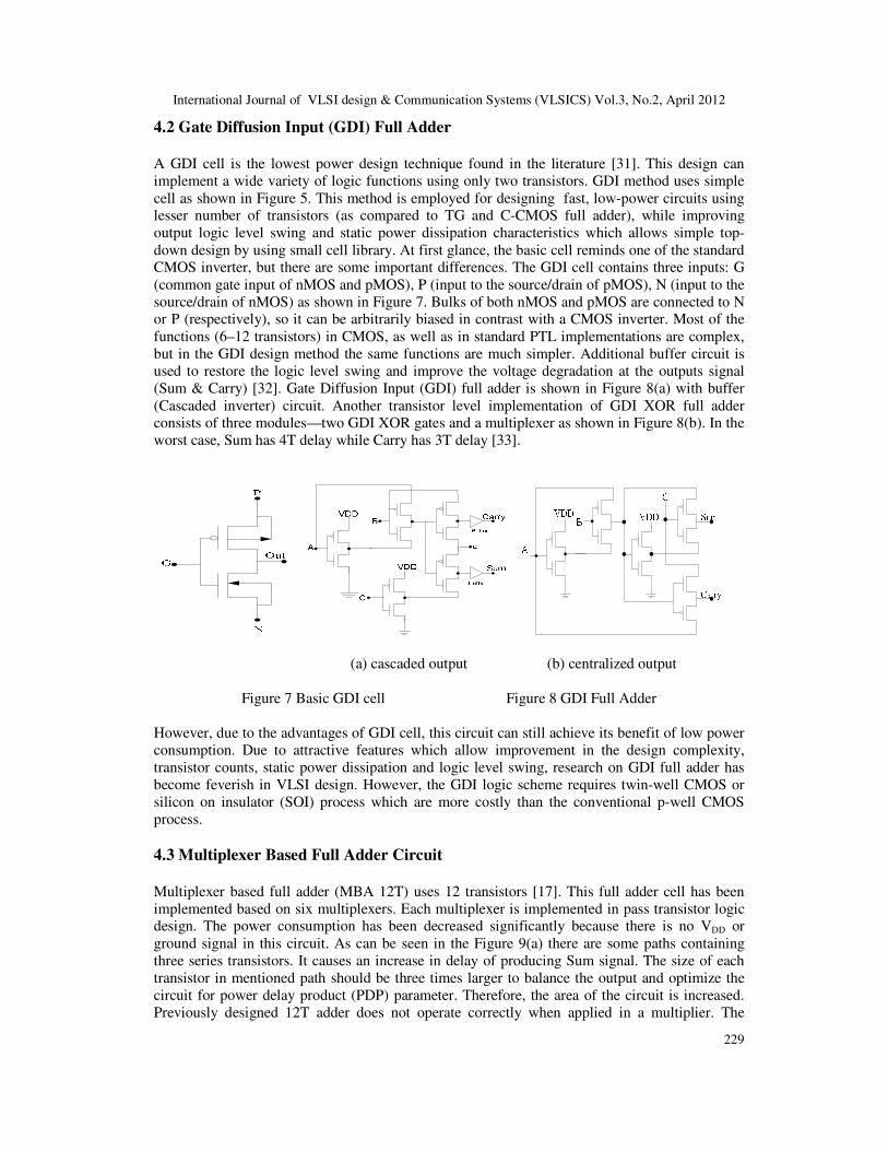
4.2 Gate Diffusion Input (GDI) Full Adder
A GDI cell is the lowest power design technique found in the literature [31]. This design can
implement a wide variety of logic functions using only two transistors. GDI method uses simple
cell as shown in Figure 5. This method is employed for designing fast, low-power circuits using lesser number of transistors (as compared to TG and C-CMOS full adder), while improving
output logic level swing and static power dissipation characteristics which allows simple top-
down design by using small cell library. At first glance, the basic cell reminds one of the standard CMOS inverter, but there are some important differences. The GDI cell contains three inputs: G
(common gate input of nMOS and pMOS), P (input to the source/drain of pMOS), N (input to the
source/drain of nMOS) as shown in Figure 7. Bulks of both nMOS and pMOS are connected to N or P (respectively), so it can be arbitrarily biased in contrast with a CMOS inverter. Most of the
functions (6–12 transistors) in CMOS, as well as in standard PTL implementations are complex,
but in the GDI design method the same functions are much simpler. Additional buffer circuit is
used to restore the logic level swing and improve the voltage degradation at the outputs signal
(Sum & Carry) [32]. Gate Diffusion Input (GDI) full adder is shown in Figure 8(a) with buffer
(Cascaded inverter) circuit. Another transistor level implementation of GDI XOR full adder consists of three modules—two GDI XOR gates and a multiplexer as shown in Figure 8(b). In the
worst case, Sum has 4T delay while Carry has 3T delay [33].
(a) cascaded output (b) centralized output
Figure 7 Basic GDI cell Figure 8 GDI Full Adder
However, due to the advantages of GDI cell, this circuit can still achieve its benefit of low power
consumption. Due to attractive features which allow improvement in the design complexity,
transistor counts, static power dissipation and logic level swing, research on GDI full adder has
become feverish in VLSI design. However, the GDI logic scheme requires twin-well CMOS or
silicon on insulator (SOI) process which are more costly than the conventional p-well CMOS
process.
4.3 Multiplexer Based Full Adder Circuit
Multiplexer based full adder (MBA 12T) uses 12 transistors [17]. This full adder cell has been
implemented based on six multiplexers. Each multiplexer is implemented in pass transistor logic design. The power consumption has been decreased significantly because there is no VDD or
ground signal in this circuit. As can be seen in the Figure 9(a) there are some paths containing
three series transistors. It causes an increase in delay of producing Sum signal. The size of each
transistor in mentioned path should be three times larger to balance the output and optimize the
circuit for power delay product (PDP) parameter. Therefore, the area of the circuit is increased.
Previously designed 12T adder does not operate correctly when applied in a multiplier. The

International Journal of VLSI design & Communication Systems (VLSICS) Vol.3, No.2, April 2012
230
reason for the failure is due to the threshold voltage losses which in turn causes error at the
output.
Figure 9 (a) MUX based Full Adder (12T) (b) 12T body-bootstrapped Full Adder
In Figure 9(b), this design (12T Body-booted-buffer) is extracted from a literature [24]. It increases the threshold voltage to reduce power dissipation. It ensures that the value for ground is
kept negative and positive for power. It uses transmission gate to produce Carry. Although it has
the advantages of improving area, speed and power consumption, it accumulates noise due to which an inverter is recommended to be added to the output. However, it requires again two more
inverters to revert it back to Carry logic function. Due to its low threshold voltage, 12T full adder
is susceptible to noise.
5. XOR-XNOR (4T) BASED HIGH SPEED LOW VOLTAGE FULL-
SWING FULL ADDER METHODOLOGIES
Adder topologies are usually based on two XOR logic circuits: First is to generate H (XOR) with
H (XNOR) logic thereafter the Sum output function is generated as shown in Figure 10. The
Carry output function is obtained by using one MUX (multiplexer) circuit.
Sum = A⊕B⊕C and Carry = A.B + C. (A⊕B)
H = A⊕B, than Sum = H⊕C and Carry = A· H + C·H
(a) Design Modules for hybrid Adder (b) Module II (c) Module III
Figure 10 Basic logic approaches for Full Adder with Full Swing output
The internal logic structure shown in Figure 10(a) has been adopted as the standard configuration
in most of the enhancements developed for the full adder module. In this configuration, the adder
module is formed by three main logical blocks: an XOR-XNOR gate to obtain (A⊕B) and (A�B)
(Module1) and XOR blocks or multiplexers to obtain the Sum and Carry outputs (Module 2 and
3). The idea of decomposing the architecture of 1-bit full adder circuit into three modules is
useful in designing a hybrid logic style. As shown in Figure 10(a) Module 1 generates the XOR
and XNOR logic functions which will be used as inputs to Module II and Module III,

International Journal of VLSI design & Communication Systems (VLSICS) Vol.3, No.2, April 2012
231
respectively. As pass transistor (4T/3T) logic has been used to implement XOR logic function
more efficiently than the complementary CMOS together with logic input (A, B, C) signals. The
Sum and Carry logic outputs are generated from Module II and III.
5.1 SERF Full Adder Circuits
The Static Energy Recovery Full adder (SERF) cell uses only 10 transistors (10T in short) and it
does not need inverted inputs. The circuit is claimed to be extremely low power because it doesn’t contain direct path to the ground and the charge stored at the load capacitance is reapplied to the
control gates (energy recovery) as shown in Figure 11(a) [23]. The elimination of the path to the
ground reduces the total power consumption by reducing the short circuit power consumption. The combination of low power and low transistor count makes the SERF adder circuit a viable
option for low power design. There are some problems in this design. First Sum is generated from
two cascaded XNOR gates (group1) which lead to long delay. Second, it cannot work correctly in
low voltage. As shown in Figure 11, in the worst case, when input signal A=B=1, there is 2Vtn
threshold loss in output voltage. Therefore, logic 1 becomes equal to VDD-2Vtn in this case. The
suitable operating supply voltage is limited to VDD> 2Vtn+|Vtp|.
5.2 10T (4T) Full Adder Topologies
The basic advantage of 10T full adders is lesser area and lower power consumption. It becomes
more and more difficult and even obsolete to keep full output voltage swing operation as the
design with fewer transistor count and lower power consumption are pursued. In pass transistor
logic, the output voltage swing may be degraded due to the threshold voltage loss problem. The
reduction in voltage swing leads to lower power consumption, but may also lead to slow
switching in the case of cascaded operation such as ripple carry adder. At low VDD operation, the
degraded output may even cause malfunction of circuit. In ref. [25] different components have
been combined to make 41 new 10T transistor full adders. Some 10T full adders are shown in Figure 11 can be designed by interchanging the inputs of the module having lowest propagation
delay among the all 10T full adder circuits. The design of the 10T adder cell is based on using an
optimized design for the XOR function and pass transistor logic to implement the addition logic function. Two XOR operations are required to calculate the Sum function. Each XOR operation
requires four transistors (4T). 2X1 MUX is used for Carry function implemented using two
transistors.
(a) SERF Adder (b) 10T Adder (c) 9A Full Adder
International Journal of VLSI design & Communication Systems (VLSICS) Vol.3, No.2, April 2012
232
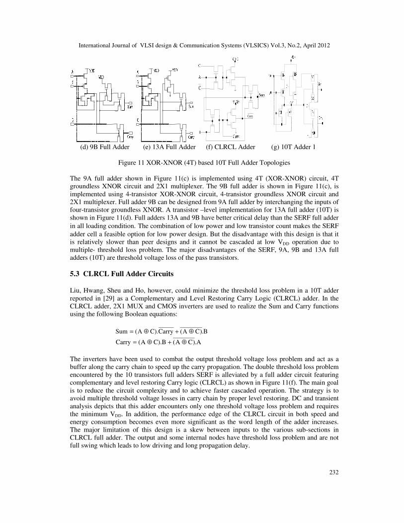
C
Carry
(d) 9B Full Adder (e) 13A Full Adder (f) CLRCL Adder (g) 10T Adder 1
Figure 11 XOR-XNOR (4T) based 10T Full Adder Topologies
The 9A full adder shown in Figure 11(c) is implemented using 4T (XOR-XNOR) circuit, 4T groundless XNOR circuit and 2X1 multiplexer. The 9B full adder is shown in Figure 11(c), is
implemented using 4-transistor XOR-XNOR circuit, 4-transistor groundless XNOR circuit and
2X1 multiplexer. Full adder 9B can be designed from 9A full adder by interchanging the inputs of four-transistor groundless XNOR. A transistor –level implementation for 13A full adder (10T) is
shown in Figure 11(d). Full adders 13A and 9B have better critical delay than the SERF full adder
in all loading condition. The combination of low power and low transistor count makes the SERF
adder cell a feasible option for low power design. But the disadvantage with this design is that it
is relatively slower than peer designs and it cannot be cascaded at low VDD operation due to
multiple- threshold loss problem. The major disadvantages of the SERF, 9A, 9B and 13A full
adders (10T) are threshold voltage loss of the pass transistors.
5.3 CLRCL Full Adder Circuits
Liu, Hwang, Sheu and Ho, however, could minimize the threshold loss problem in a 10T adder
reported in [29] as a Complementary and Level Restoring Carry Logic (CLRCL) adder. In the
CLRCL adder, 2X1 MUX and CMOS inverters are used to realize the Sum and Carry functions using the following Boolean equations:
B.)CA(CarryC).A(Sum ⊕+⊕= A.)CA(C).BA(Carry ⊕+⊕=
The inverters have been used to combat the output threshold voltage loss problem and act as a
buffer along the carry chain to speed up the carry propagation. The double threshold loss problem
encountered by the 10 transistors full adders SERF is alleviated by a full adder circuit featuring
complementary and level restoring Carry logic (CLRCL) as shown in Figure 11(f). The main goal
is to reduce the circuit complexity and to achieve faster cascaded operation. The strategy is to avoid multiple threshold voltage losses in carry chain by proper level restoring. DC and transient
analysis depicts that this adder encounters only one threshold voltage loss problem and requires
the minimum VDD. In addition, the performance edge of the CLRCL circuit in both speed and
energy consumption becomes even more significant as the word length of the adder increases.
The major limitation of this design is a skew between inputs to the various sub-sections in
CLRCL full adder. The output and some internal nodes have threshold loss problem and are not
full swing which leads to low driving and long propagation delay.
International Journal of VLSI design & Communication Systems (VLSICS) Vol.3, No.2, April 2012
233
Reported 10T full adder1 cell based on low power XNOR (4T) [38] pass-transistor logic design
and transmission gates are shown in Figure11 (g). XNOR signal is used as the selector of two
multiplexers. XNOR signal has VT threshold loss. Output multiplexers have threshold loss too.
Therefore, this circuit has threshold loss problem as well as SERF circuit. Intermediate signal
XNOR drives two PMOS and two NMOS transistor gates. Carry and Sum generator functions are
two multiplexers uses only two transistors. There are not any VDD and ground these components
therefore these components consume low power. Simplicity of the carry generator and sum
generator circuits are another reason to decrease power and delay in these circuits. There is a semi
inverter to invert input A. This inverter should work only when XNOR signal is equal to logic 0.
Therefore, we use XNOR signal as ground of the inverter to decrease short circuit and leakage
power in the inverter.
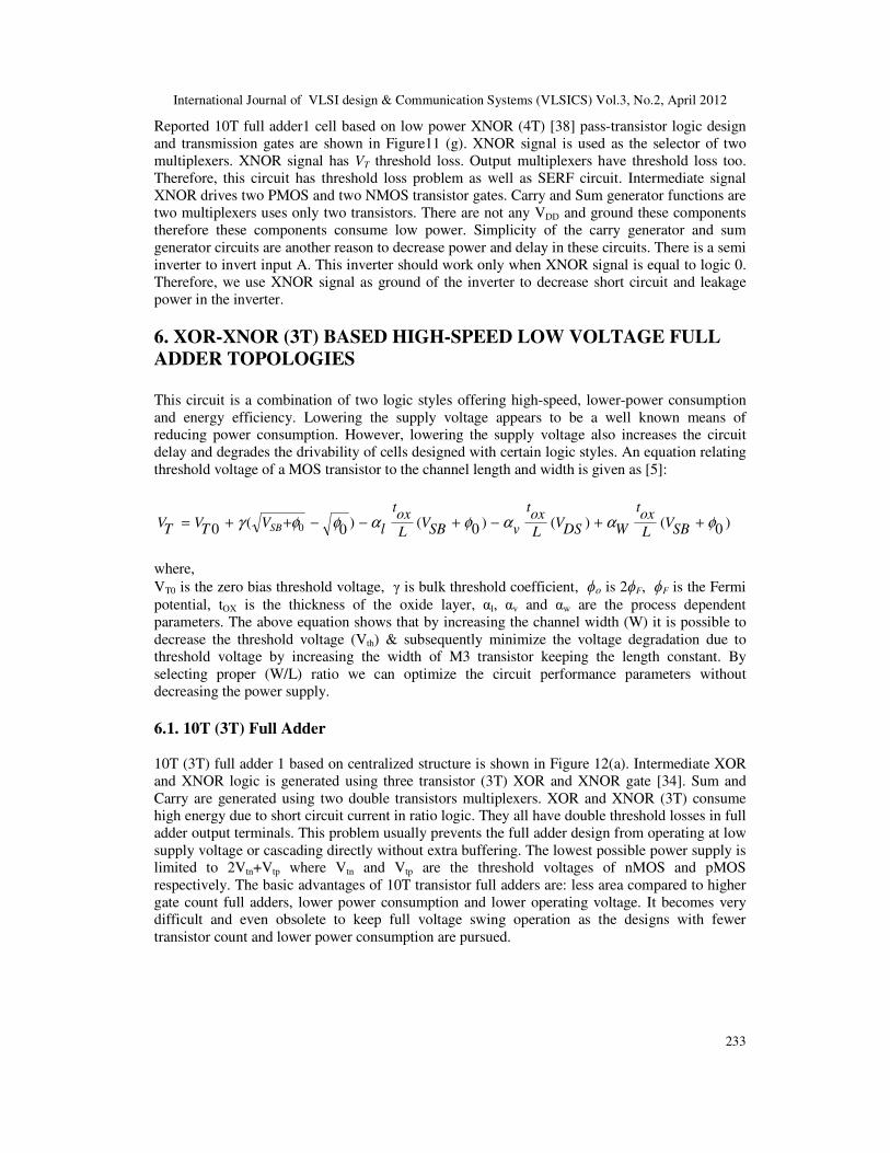
6. XOR-XNOR (3T) BASED HIGH-SPEED LOW VOLTAGE FULL
ADDER TOPOLOGIES
This circuit is a combination of two logic styles offering high-speed, lower-power consumption
and energy efficiency. Lowering the supply voltage appears to be a well known means of reducing power consumption. However, lowering the supply voltage also increases the circuit
delay and degrades the drivability of cells designed with certain logic styles. An equation relating
threshold voltage of a MOS transistor to the channel length and width is given as [5]:
)0()()0()0
(0 0 φααφαφφγ ++−+−−++= SBVL
oxt
WDSVL
oxt
vSBVL
oxt
lVTVTV SB
where,
VT0 is the zero bias threshold voltage, γ is bulk threshold coefficient, ϕo is 2ϕF, ϕF is the Fermi
potential, tOX is the thickness of the oxide layer, αl, αv and αw are the process dependent
parameters. The above equation shows that by increasing the channel width (W) it is possible to
decrease the threshold voltage (Vth) & subsequently minimize the voltage degradation due to threshold voltage by increasing the width of M3 transistor keeping the length constant. By
selecting proper (W/L) ratio we can optimize the circuit performance parameters without
decreasing the power supply.
6.1. 10T (3T) Full Adder
10T (3T) full adder 1 based on centralized structure is shown in Figure 12(a). Intermediate XOR
and XNOR logic is generated using three transistor (3T) XOR and XNOR gate [34]. Sum and
Carry are generated using two double transistors multiplexers. XOR and XNOR (3T) consume high energy due to short circuit current in ratio logic. They all have double threshold losses in full
adder output terminals. This problem usually prevents the full adder design from operating at low
supply voltage or cascading directly without extra buffering. The lowest possible power supply is limited to 2Vtn+Vtp where Vtn and Vtp are the threshold voltages of nMOS and pMOS
respectively. The basic advantages of 10T transistor full adders are: less area compared to higher
gate count full adders, lower power consumption and lower operating voltage. It becomes very difficult and even obsolete to keep full voltage swing operation as the designs with fewer
transistor count and lower power consumption are pursued.
International Journal of VLSI design & Communication Systems (VLSICS) Vol.3, No.2, April 2012
234
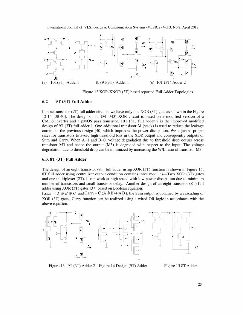
(a) 10T(3T) Adder 1 (b) 9T(3T) Adder 1 (c) 10T (3T) Adder 2
Figure 12 XOR-XNOR (3T) based reported Full Adder Topologies
6.2 9T (3T) Full Adder
In nine transistor (9T) full adder circuits, we have only one XOR (3T) gate as shown in the Figure
12-14 [38-40]. The design of 3T (M1-M3) XOR circuit is based on a modified version of a CMOS inverter and a pMOS pass transistor. 10T (3T) full adder 2 is the improved modified
design of 9T (3T) full adder 1. One additional transistor M (stack) is used to reduce the leakage
current in the previous design [40] which improves the power dissipation. We adjusted proper
sizes for transistors to avoid high threshold loss in the XOR output and consequently outputs of
Sum and Carry. When A=1 and B=0, voltage degradation due to threshold drop occurs across
transistor M3 and hence the output (M3) is degraded with respect to the input. The voltage
degradation due to threshold drop can be minimized by increasing the W/L ratio of transistor M3.
6.3. 8T (3T) Full Adder
The design of an eight transistor (8T) full adder using XOR (3T) function is shown in Figure 15. 8T full adder using centralizer output condition contains three modules—Two XOR (3T) gates
and one multiplexer (2T). It can work at high speed with low power dissipation due to minimum
number of transistors and small transistor delay. Another design of an eight transistor (8T) full
adder using XOR (3T) gates [37] based on Boolean equation:
( CBASum ⊕⊕= and B.A)BA.(CCarry +⊕= ), the Sum output is obtained by a cascading of
XOR (3T) gates. Carry function can be realized using a wired OR logic in accordance with the
above equation.
Figure 13 9T (3T) Adder 2 Figure 14 Design (9T) Adder Figure 15 8T Adder

International Journal of VLSI design & Communication Systems (VLSICS) Vol.3, No.2, April 2012
235
7. NEW SUM (XOR-XNOR) FUNCTION BASED HIGH- SPEED LOW
VOLTAGE FULL-SWING ADDER TOPOLOGIES
New hybrid circuit is a designed combination of TG with PT logic style that shows high-speed and energy efficiency. The propose circuits have the least number of transistors and no
complementary input signals are required. Designed structure of a XOR based full adder consists
of one exclusive OR/NOR function (XOR /XNOR), two transmission gates in the middle, and one XOR gate in the right. The complementary outputs of the XOR/XNOR gate are used to
control the transmission gate which realizes a multiplexer circuit producing the Carry output
function. Intermediate XOR and XNOR function output is generated using four transistors (4T) and CMOS inverter respectively. Two cross-coupled pMOS transistors arrangement that
eliminates the non-swing operation at low voltage, are connected between XOR and XNOR
function outputs. The complementary outputs of the XOR & XNOR logic gate are used to control
the transmission gate which together realizes a Sum output function with pass transistors.
New design approach to generate the XOR and XNOR functions is to synthesize the XOR
function and generate the XNOR function through a CMOS inverter. The XOR/XNOR (3T)
function is used in a designed full swing full adder circuits at low voltage as shown in Figure 17
[41-43]. In New design full adder circuits M1, M2 and M3 transistors are used as XOR function and the output of CMOS inverter (M4 & M5) is XNOR logic function. In design (9T) Sum and
Carry outputs are generated by two pass-transistor (M6 & M7) and (M8 & M9) logic circuits
respectively. In other designs TG (M6, M7) and TG (M8, M9) gives the Carry output and restores
output swing. TG (M10, M11) and pass transistor (M12, M13) are used for Sum output and
restore the output swing as shown in Figure 13. It implements the complementary pass-transistor
logic to drive the load.
A second approach is to use different set of transistors to generate the XOR and XNOR function
separately, with the possibility of introducing a large transistor count. To reduce the number of
transistors, we use a similar pass transistor circuits with six transistors to generate the XOR and XNOR functions simultaneously. A novel 16-transistor full adder circuit [43] that generates
XOR-XNOR outputs simultaneously is shown in Figure 17. Similarly in the design2 full adder
circuit M1, M2 and M3 are used as XOR and the output of M4, M5 and M6 is XNOR circuit. The cross-coupled PMOS transistors are connected between XOR and XNOR output to alleviate
threshold problem for all possible input combination at low voltage and reduce short-circuit
power dissipation. The cross-coupled two pMOS transistors (M7, M8) are connected between
XOR and XNOR outputs to eliminate the non-swing operation at low voltage.
Figure 16 Design1 Full Adder Figure 17(a) Design2 Full Adder (b) Design3 Full Adder
International Journal of VLSI design & Communication Systems (VLSICS) Vol.3, No.2, April 2012
236
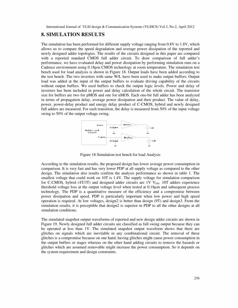
8. SIMULATION RESULTS
The simulation has been performed for different supply voltage ranging from 0.8V to 1.8V, which
allows us to compare the speed degradation and average power dissipation of the reported and
newly designed adder topologies. The results of the circuits designed in this paper are compared
with a reported standard CMOS full adder circuit. To draw comparison of full adder’s performance, we have evaluated delay and power dissipation by performing simulation runs on a
Cadence environment using 0.18µm CMOS technology at room temperature. The simulation test
bench used for load analysis is shown in Figure 18. Output loads have been added according to the test bench. The two inverters with same W/L have been used to make output buffers. Output
load was added at the input of the output buffers to evaluate driving capability of the circuits
without output buffers. We used buffers to check the output logic levels. Power and delay of
inverters has been included in power and delay calculation of the whole circuit. The transistor
size for buffers are two for pMOS and one for nMOS. Each one-bit full adder has been analyzed
in terms of propagation delay, average power dissipation and their product. The value of delay,
power, power-delay product and energy delay product of C-CMOS, hybrid and newly designed
full adders are measured. For each transition, the delay is measured from 50% of the input voltage
swing to 50% of the output voltage swing.
Figure 18 Simulation test bench for load Analysis
According to the simulation results, the proposed design has lower average power consumption in
comparison. It is very fast and has very lower PDP at all supply voltage as compared to the other
design. The simulation also results confirm the analysis performance as shown in table 1. The
smallest voltage that could work on 10T is 1.4V. The supply voltage for simulation comparison
for C-CMOS, hybrid (4T/3T) and designed adder circuits are 1V VDD. 10T adders experience threshold voltage loss at the output voltage level when tested at 0.18µm and subsequent process
technology. The PDP is a quantitative measure of the efficiency and a compromise between
power dissipation and speed. PDP is particularly important when low power and high speed operation is required. At low voltages, design2 is better than design (9T) and design3. From the
simulation results, it is perceptible that design2 is superior in PDP to all the other designs at all
simulation conditions.
The simulated snapshot output waveforms of reported and new design adder circuits are shown in
Figure 19. Newly designed full adder circuits are classified as full swing output because they can
be operated at less than 1V. The simulated snapshot output waveform shows that there are glitches on signals which are inevitable in any combinational circuit. The removal of these
glitches is a compromise because on one hand, having glitches might cause power consumption in
the output buffers or stages whereas on the other hand adding circuits to remove the hazards or glitches which are assumed removable might increase the power consumption. So it depends on
the system requirement and design constraints.

International Journal of VLSI design & Communication Systems (VLSICS) Vol.3, No.2, April 2012
(a) Design1 Full Adder
Figure 19 Simulated snapshot
Figure 20
0
10
20
30
40
50
60
70
0.8 1
14T(4T) SERF(4T)
8T(3T) Design(9T)
De
lay(p
s)
Voltage
International Journal of VLSI design & Communication Systems (VLSICS) Vol.3, No.2, April 2012
(b) Design2 Full Adder (c) Design3 Full Adder
Simulated snapshot of Input - Output waveforms at 0.8V VDD
20(a) Delay comparisons of Full Adder cells
1.2 1.4 1.6
SERF(4T) 9A(4T) 10T(4T) Design1(4T)
Design(9T) Design2 (3T) Design 3(3T)
Voltage
International Journal of VLSI design & Communication Systems (VLSICS) Vol.3, No.2, April 2012
237
(c) Design3 Full Adder
DD
1.8
Design1(4T)

International Journal of VLSI design & Communication Systems (VLSICS) Vol.3, No.2, April 2012
238
Figure 20(b) Power (µW) comparison of Full Adder cells
High-speed of the designed full adders is due to the short path between input and output logic
circuit. Simulation results (Fig. 20a) shows that design3 is the best circuit in terms of speed at all
voltages since XOR & XNOR logic is generated separately in a single circuit. It enjoys high delay
and high sensitivity against voltage scaling. Design3 is miles ahead of design1 and shows better
performance even than design (9T) full adder. Design (9T) full adder has minimum number of
transistors but high delay because XNOR logic function is generated using XOR with CMOS
inverter. However, at all supply voltage variations design2 is faster than Design (9T) full adder.
Figure 20(b) shows that the newly design1 full adder is the most power consuming circuit at
1.8V. The power consumption worsens as we increase the supply voltage. Design2 has the lowest
power consumption in comparison to the other simulated adder circuits. It worked successfully
even at low voltage. Design1 full adder consumes higher power due to the use of high power
consuming XOR (3T) and XNOR (3T) gate in a single unit.
8.1. Driving Capability (Load) Analysis
To evaluate the driving capability of the designed adder cells, they are simulated using several
output load capacitance, ranged from 2fF to 500fF at the previously mentioned simulation
conditions. The simulation test bench used for load analysis is shown in Figure 15. Output loads
have been added according to the test bench. The two inverters with same W/L have been used to
make output buffers. Output load was added at the input of the output buffers to evaluate driving
capability of the circuits without output buffers. We used buffers to check the output logic levels.
Power and circuit delay of inverters have been included in power and delay calculation of the
whole circuit. The transistor size for buffers are two for pMOS and one for nMOS. A fixed value
1fF capacitance has been added at the output of the buffer circuit. Minimum output load for all
the simulation is 2fF, except for the case, in which we study the effect of output load on full
adder. The effect of output load capacitance as it changes from 2fF to 500fF is shown in Table 1-
2.
8.2. Immunity to Noise Comparison Analysis
To test the immunity of the circuits to the ambient temperature noise and variations, the designs
are simulated in a vast range of temperature range from 0oC to 70
oC at the previously mentioned
simulation conditions. Power dissipation, propagation delay, PDP and EDP factors of the
0
0.5
1
1.5
2
0.8 1 1.2 1.4 1.6 1.8
14T(4T) SERF(4T) 9A(4T) 10T(4T) Design1(4T)
8T(3T) Design(9T) Design2 (3T) Design 3(3T)
Voltage
Po
we
r (µ
w)

International Journal of VLSI design & Communication Systems (VLSICS) Vol.3, No.2, April 2012
239
designed circuits are simulated only at 0.8V and 1.8V for 0.18µm CMOS technology. However,
simulation results show that the newly designed circuits can work at other supply voltages also
and it is completely robust to voltage variations. The new designs are immune to the supply
voltage noise and possible voltage variations. The circuits are simulated at 0.8, 1, 1.2, 1.4, 1.6 and
1.8V. At these voltages, the designed circuits work satisfactorily. Working with different supply
voltage, with the best PDP and EDP at 0.8V, we demonstrate that supply voltage variations noise
does not affect the functionality of the circuit. One important factor from the noise perspective
that should be taken into consideration is the immunity of the circuit to the ambient temperatures.
8.3. Layout Area Analysis
The transistors that are used in XOR-XNOR (3T) based full adder designed circuits (13T & 16T)
are using 3T XOR logic. Thus the area overhead of the designed circuits are lower than that of the
reported conventional adders and also some other adder circuits [41]. By optimizing the transistor
size of the considered full adders, it is feasible to reduce the delay of all the adders without
significantly increasing the power consumption. Moreover the transistor sizes can be set to
achieve minimum power delay product (PDP). All adders were designed with minimum transistor
sizes initially and then simulated.
Table 1: Simulation results comparisons for delay and power at 2fF load capacitor
Design Delay (ps) with 2fF load capacitance Power (µw) with 2fF load Capacitance
Voltage 1.8V 1.6V 1.4V 1.2V 1V 0.8V 1.8V 1.6V 1.4V 1.2V 1V 0.8V
CMOS 206 237 284 366 528 961 7.7 5.7 4.27 3.1 2.1 1.29
TG 119 135 160 202 284 494 9.7 7.41 5.4 3.4 2.1 1.22
Design1 111 128 158 218 369 1060 12 7.5 4.6 2.6 1.3 0.65
Design2 123 140 166 208 290 500 3 2.3 1.8 1.2 0.27 0.5
Design3 97 110 130 164 230 398 70 50 34 21 11 4.8
Table 2: Simulation results comparisons for delay and power at at 1.8V
Design Delay (ps) with load capacitance variation Power (µw) with load Capacitance variation
Load
Cap
2fF 10fF 50fF 100fF 200fF 500fF 2fF 10fF 50fF 100fF 200fF 500fF
CMOS 224 309 625 990 1700 3800 7.7 16 28 49 78 100
TG 119 168 412 707 1280 2958 9.8 11 15 21 33 58
Design1 110 119 166 226 347 723 12 13 18 21 24 38
Design2 123 180 460 2150 4300 6900 3 3.4 7 17 22 35
Design3 97 128 277 463 850 1960 70 72 78 86 96 116
9. CONCLUSIONS
In this paper, new low-voltage high performance CMOS full adder circuits are discussed. The
new designs are derived by combining XOR (XNOR) (4T/3T) gates. The new design full adders
can provide full voltage swing at a low supply voltage and offer superior performance in respect
of both power and speed as compared to the conventional full adders. Various circuits based on

International Journal of VLSI design & Communication Systems (VLSICS) Vol.3, No.2, April 2012
240
different combinations of XOR function and TG with PT (powerless/groundless) circuit have
been implemented, simulated, analyzed and compared. Different full adder logic styles in
combination with using the adder categorization and hybrid-CMOS design style, many full adders
can be conceived. As an example, new full adders designed using hybrid-CMOS style with PT
style have been presented in this paper that target low PDP. The compared simulation result
shows that the performance of the new designs is far superior to the other reference designs of full
adder circuits under different load conditions and simulation parameters. It is also evident that the
newly designed circuit has the advantages of good signal output levels and the lowest PDP at low
supply voltage.
REFERENCES
[1] John P. Uyemura, (2002) Introduction to VLSI Circuits and Systems, John Wiley & Sons.
[2] Sung-Mo Kang, Y. Leblebici, (2005) CMOS Digital Integrated Circuits: Analysis and Design, Tata
McGraw Hill, New York,NY,USA.
[3] N. Weste and D. Harris, (2005) CMOS VLSI Design, Pearson Wesley.
[4] N. Zhuang and H. Wu, (1992) “A new design of the CMOS full adder,” IEEE Journal of Solid-State
Circuits, Vol. 27, No. 5, pp. 840–844.
[5] Y.Tsividis, (1996) Mixed Analog- Digital VLSI Devices and Technology, Singapore; McGraw Hill.
[6] K.M. Chu and D. Puffrey, (1987) “A Comparison of CMOS Circuit Techniques Differential Cascode
Voltage Switch Logic versus Conventional Logic,” IEEE Journal of Solid-State Circuit, Vol. SC 22,
No. 4, pp. 528- 532.
[7] A. P. Chandrakasan, S. Sheng and R. W. Bordersen, (1992) “Low-power CMOS digital design,”
IEEE Journal of Solid-State Circuits, Vol. 27, No. 4, pp. 473- 484.
[8] E. Abu-Sharma and M. Bayoumi, (1995) “A new cell for low power adders,” in Proceeding of
International Midwest Symposium Circuits System, pp. 1014-1017.
[9] I. S. Abu-Khater, A. Bellaouar, and M.I. Elmasry, (1996) “Circuit techniques for CMOS low power
high performance multipliers,” IEEE Journal of Solid- State Circuits, Vol. 31, No. 10, pp. 1535-1546.
[10] Uming Ko, Poras T. Balsara and Wai Lee, (1995) “Low-Power Design Techniques for High-
Performance CMOS adders,” IEEE Transactions on Very Large Scale Integration (VLSI) Systems,
Vol. 3, No. 2, pp. 327-333.
[11] A. Bellaouar and M. I. Elmasry, (1995) Low-Power Digital VLSI Design: Circuits and Systems,
Kluwer Academic.
[12] A. Parameswar, H. Hara and T. Sakurai, (1994) “A high speed, low power, swing restored pass-
transistor logic based multiply and accumulate circuit for multimedia applications,” in Proceedings of
IEEE Custom Integrated Circuits Conference, San Diego, USA, pp. 278–281.
[13] A. Parameswar, H. Hara and T. Sakurai, (1996) “A swing restored pass-transistor logic-based multiply
and accumulate circuit for multimedia applications,” IEEE Journal of Solid-State Circuits, Vol. 31,
No. 6, pp. 804–809.
[14] K. Yano, Y. Sasaki, K. Rikino and K. Seki, (1996) “Top-down pass-transistor logic design,” IEEE
Journal of Solid-State Circuits, Vol. 31,No. 6, pp. 792–803.
[15] Reto Zimmermann and Wolfgang Fichtner, (1997) “Low-power Logic Styles: CMOS versus pass
transistor logic,” IEEE Journal of Solid-State Circuits, Vol. 32, No. 7, pp. 1079-1090.
[16] Ahmed M. Shams, and Magdy A. Bayoumi, (2000) “A Novel High- Performance CMOS 1-Bit Full-
Adder Cell,” IEEE Transaction on Circuits and Systems. II, Vol. 47, No. 5, pp. 478–481.
[17] Abdulkarim Al-Sheraidah, Yingtao Jiang, Yuke Wang and Edwin Sha, (2001) “A Novel Low Power
Multiplexer-Based Full Adder,” European Conference on Circuit Theory and Design, Espoo, Finland,
pp. I329-I332.
[18] D. Radhakrishnan, (2001) “Low-voltage low-power CMOS Full Adder,” IEE Proceedings Circuit:
Devices and Systems, Vol. 148, No. 1, pp. 19-24.
[19] Fartash Vasefi and Z. Abid, (2005) “Low Power N-bit Adders and Multiplier using lowest number of
Transistors 1-bit Adders,” in Proceedings of IEEE Conference CCECE/CCGEI, 05 Saskatoon, pp.
1731-1734.
[20] Sumeer Goel, Ashok Kumar, Magdy A. Bayouni, (2006) “Design of Robust, Energy-Efficient Full
Adders for Deep-Submicrometer Design Using Hybrid-CMOS Logic Style,” IEEE Transactions on
Very Large Scale Integration (VLSI) Systems, Vol. 14, No. 12, pp. 1309-1321.

International Journal of VLSI design & Communication Systems (VLSICS) Vol.3, No.2, April 2012
241
[21] Ahmed M. Shams, Tarek K. Darwish, and Magdy A. Bayoumi, (2002) “Performance Analysis of
Low-Power 1-Bit CMOS Full Adder Cells,” IEEE Transactions on Very Large Scale Integration
(VLSI) Systems, Vol. 10, No. 1, pp. 20–29.
[22] Mark Vesterbacka, (1999) “14-Transistor CMOS Full Adder with Full Voltage-Swing Nodes,” in
Proceedings of IEEE Workshop Signal Processing Systems, pp. 713-722.
[23] R. Shalem, E. John and L. K. John, (1999) “Novel Low Power Energy Recovery Full Adder Cell,” in
Proceeding of 9th
Great Lakes Symposium on VLSI (GLSVLSI’99), pp. 380–383.
[24] Y. Jiang, A. Al-Sheraidah, Y. Wang, E. Shah, and J. Chung, (2004) “A Novel Multiplexer-Based Low
Power Full Adder,” IEEE Transactions on Circuits and Systems, Vol. 51, No. 7, pp. 345-348.
[25] Hung Tien Bui, Yuke Wang and Yingtao Jiang, (2002) “Design and Analysis of Low-Power 10-
Transistor Full Adders Using Novel XOR-XNOR Gates,” IEEE Transactions on Circuits and Systems
II: Analog and Digital Signal Processing, Vol. 49, No. 1, pp. 25-30.
[26] S. Wairya, Himanshu Pandey, R. K. Nagaria and S. Tiwari, (2010) “Ultra Low Voltage High Speed 1-
Bit CMOS Adder,” in Proceedings of IEEE International Conference on Power, Control and
Embedded System (ICPCES’10), India, pp. 1-6.
[27] Chip-Hong Chang, Jiangmin Gu, Mingyan Zhang, (2005) “A Review of 0.18µm Full Adder
Performances for Tree Structured Arithmetic Circuits,” IEEE Transaction on Very Large Scale
Integration (VLSI) Systems, Vol. 13, No. 6, pp. 686-694.
[28] Sumeer Goel, Mohammed A. Elgamel, Magdy A. Bayoumi, Yasser Hanafy, (2006) “Design
Methodologies for High-Performance Noise-Tolerant XOR-XNOR Circuits,” IEEE Transactions on
Circuits and Systems- I, Vol. 53, No. 4, pp. 867-878.
[29] Jin-Fa-Lin, Yin-Tsung Hwang, Ming-Hwa Sheu, and Cheng-Che Ho, (2007) “A Novel High-Speed
and Energy Efficient 10-Transistor Full Adder Design,” IEEE Transaction on Circuits and Systems I,
Vol. 54, No. 5, pp. 1050-1059.
[30] S. Veeramachaneni, M. B. Srinivas, (2008) “New Improved 1-Bit Full Adder Cells,” CCECE /CCGEI,
May 5-7, 2008, Niagara Falls, Ontano, Canada, pp. 735-738,.
[31] Arkadiy Morgenshtein, , Alexander Fish and Israel A. Wagner, (2002) “Gate-Diffusion Input (GDI):
A Power Efficient Method for Digital Combinatorial Circuits,” IEEE Transactions on Very Large
Scale Integration (VLSI) Systems, Vol. 10 No. 5, pp. 566 -581
[32] Adarsh Kumar Agrawal, S. Wairya, R. K. Nagaria and S. Tiwari, (2009) “A New Mixed Gate
Diffusion Input Full Adder Topology for High Speed Low Power Digital Circuits,” World Applied
Sciences Journal (WASJ) 7 (Special Issue of Computer & IT): pp. 138-144.
[33] Mohammad Hossein Moaiyeri and Reza Faghih Mirzaee, (2009) “Two New Low-Power and High-
Performance Full Adders,” Journal of Computers, Vol. 4, No. 2, pp. 119-126.
[34] MA Elgmal, S. Goel and M.A. Bayoumi, (2003) “Noise Tolerant Low Voltage XOR-XNOR for Fast
Arithmetic,” in Proceeding of IEEE Great Lakes Symposium on VLSI (GLSVLSI’ 03), 2003,Wasting
D.C., pp. 285-288.
[35] Shiv Shankar Mishra, S. Wairya, R.K. Nagaria and S. Tiwari, (2009) “New Design Methodologies for
High Speed Low Power XOR-XNOR Circuits,” Journal of World Academy Science, Engineering and
Technology (WASET), Vol. 55, No. 35, pp. 200-206.
[36] S. Wairya, R. K. Nagaria and S. Tiwari, (2010) “A Novel CMOS Full Adder Topology for Low
Voltage VLSI Applications,” in Proceeding of International Conference on Emerging Trends in
Signal Processing & VLSI Design (SPVL’10)’, Hyderabad, India, pp. 1142-1146.
[37] Shubhajit Roy Chowdhury, Aritra Banerjee, Aniruddha Roy and H. Saha, (2008) “A high Speed 8
Transistor Full Adder Design using Novel 3 Transistor XOR Gates,” International Journal of
Electronics, Circuits and Systems, WASET Fall, Vol. 2, No. 4, pp. 217-223.
[38] Mariano Aguirre-Hernandez and Monico Linares-Aranda, (2011) “CMOS Full Adders for Energy-
Efficient Arithmetic Application,” IEEE Transactions on Very Large Scale Integration (VLSI)
System, Vol. 19, No. 4, pp. 718-721.
[39] M. Hosseinghadiry, H. Mohammadi, M. Nadisenejani, (2009) “Two New Low Power High
Performance Full Adders with Minimum Gates,” International Journal of Electronics, Circuits and
Systems, Vol. 3, No. 2, pp. 124-131.
[40] Subodh Wairya, Rajendra Kumar Nagaria and Sudarshan Tiwari, (2011) “New Design Methodologies
for High-Speed Low-Voltage 1 Bit CMOS Full Adder Circuits,” Journal of Computer Technology
and Application, Vol. 2, No. 3, pp. 190-198.
[41] Subodh Wairya, Rajendra Kumar Nagaria and Sudarshan Tiwari, (2011) “New Design Methodologies
for High Speed Mixed Mode Full Adder Circuits,” International Journal of VLSI and Communication
Systems, Vol. 2, No. 2, pp. 78-98.

International Journal of VLSI design & Communication Systems (VLSICS) Vol.3, No.2, April 2012
242
[42] Subodh Wairya , Garima Singh, Vishant, R. K. Nagaria and S. Tiwari (2011), “Design Analysis of
XOR (4T) based Low Voltage CMOS Full Adder Cell,” In Proceeding of IEEE International
Conference on Current Trends In Technology (NUiCONE’11), Ahmedabad, India pp. 1-7.
[43] Subodh Wairya, Rajendra Kumar Nagaria and Sudarshan Tiwari, (2012) “Performance Analysis of
High Speed Hybrid CMOS Full Adder Circuits for Low Voltage VLSI Design,” VLSI Design, Vol.
2012, Article ID 173079, 18 pages.