comparative analysis of magnetically coupled Z-source inverters
8
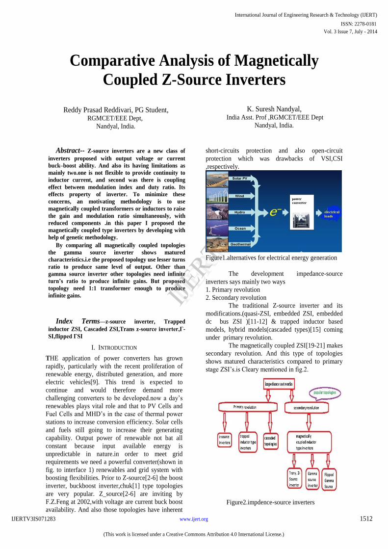
Abstract-- Z-source inverters are a new class of inverters proposed with output voltage or current buck–boost ability. And also its having limitations as mainly two.one is not flexible to provide continuity to inductor current, and second was there is coupling effect between modulation index and duty ratio. Its effects property of inverter. To minimize these concerns, an motivating methodology is to use magnetically coupled transformers or inductors to raise the gain and modulation ratio simultaneously, with reduced components .in this paper I proposed the magnetically coupled type inverters by developing with help of genetic methodology. By comparing all magnetically coupled topologies the gamma source inverter shows matured characteristics.i.e the proposed topology use lesser turns ratio to produce same level of output. Other than gamma source inverter other topologies need infinite turn’s ratio to produce infinite gains. But proposed topology need 1:1 transformer enough to produce infinite gains. Index Terms—z-source inverter, Trapped inductor ZSI, Cascaded ZSI,Trans z-source inverter,Γ- SI,flipped ΓSI I. INTRODUCTION THE application of power converters has grown rapidly, particularly with the recent proliferation of renewable energy, distributed generation, and more electric vehicles[9]. This trend is expected to continue and would therefore demand more challenging converters to be developed.now a day’s renewables plays vital role and that to PV Cells and Fuel Cells and MHD’s in the case of thermal power stations to increase conversion efficiency. Solar cells and fuels still going to increase their generating capability. Output power of renewable not bat all constant because input available energy is unpredictable in nature.in order to meet grid requirements we need a powerful converter(shown in fig. to interface 1) renewables and grid system with boosting flexibilities. Prior to Z-source[2-6] the boost inverter, buckboost inverter,chuk[1] type topologies are very popular. Z_source[2-6] are inviting by F.Z.Feng at 2002,with voltage are current buck boost availability. And also those topologies have inherent short-circuits protection and also open-circuit protection which was drawbacks of VSI,CSI ,respectively. Figure1.alternatives for electrical energy generation The development impedance-source inverters says mainly two ways 1. Primary revolution 2. Secondary revolution The traditional Z-source inverter and its modifications.(quasi-ZSI, embedded ZSI, embedded dc bus ZSI )[11-12] & trapped inductor based models, hybrid models(cascaded types)[15] coming under primary revolution. The magnetically coupled ZSI[19-21] makes secondary revolution. And this type of topologies shows matured characteristics compared to primary stage ZSI’s.is Cleary mentioned in fig.2. Figure2.impdence-source inverters Comparative Analysis of Magnetically Coupled Z-Source Inverters Reddy Prasad Reddivari, PG Student, RGMCET/EEE Dept, Nandyal, India. K. Suresh Nandyal, India Asst. Prof ,RGMCET/EEE Dept Nandyal, India. Vol. 3 Issue 7, July - 2014 International Journal of Engineering Research & Technology (IJERT) ISSN: 2278-0181 www.ijert.org IJERTV3IS071283 (This work is licensed under a Creative Commons Attribution 4.0 International License.) 1512
-
Upload
reddyprasad-reddivari -
Category
Engineering
-
view
42 -
download
0
Transcript of comparative analysis of magnetically coupled Z-source inverters
Abstract--
Z-source inverters are a new class of
inverters proposed
with output voltage or current
buck–boost ability.
And also its having limitations as
mainly two.one is not flexible to provide continuity to
inductor current, and second was there is coupling
effect between modulation index and duty ratio. Its
effects property of inverter.
To minimize these
concerns, an
motivating methodology is to use
magnetically coupled transformers
or inductors to raise
the gain and modulation ratio simultaneously,
with
reduced components .in this paper I proposed the
magnetically coupled type inverters by developing with
help of genetic methodology.
By comparing all magnetically coupled topologies
the gamma source inverter shows matured
characteristics.i.e the proposed topology use lesser turns
ratio to produce same level of output. Other than
gamma source inverter other topologies need infinite
turn’s ratio to produce infinite gains. But proposed
topology need 1:1 transformer enough to produce
infinite gains.
Index Terms—z-source inverter, Trapped
inductor ZSI, Cascaded ZSI,Trans z-source inverter,Γ-
SI,flipped ΓSI
I. INTRODUCTION
THE application of power converters has grown
rapidly, particularly with the recent proliferation of
renewable energy, distributed generation, and more
electric vehicles[9]. This trend is expected to
continue and would therefore demand more
challenging converters to be developed.now a day’s
renewables plays vital role and that to PV Cells and
Fuel Cells and MHD’s in the case of thermal power
stations to increase conversion efficiency. Solar cells
and fuels still going to increase their generating
capability.
Output power of renewable not bat all
constant because input available energy is
unpredictable in nature.in order to meet grid
requirements we need a powerful converter(shown in
fig. to interface 1) renewables and grid system with
boosting flexibilities. Prior to Z-source[2-6]
the boost
inverter, buckboost inverter,chuk[1]
type topologies
are very popular. Z_source[2-6]
are inviting by
F.Z.Feng at 2002,with voltage are current buck boost
availability. And also those topologies have inherent
short-circuits
protection and also open-circuit
protection which was drawbacks of VSI,CSI
,respectively.
Figure1.alternatives for electrical energy generation
The development impedance-source
inverters says mainly two ways
1. Primary revolution
2. Secondary revolution
The traditional Z-source inverter and its
modifications.(quasi-ZSI, embedded ZSI, embedded
dc bus ZSI )[11-12]
& trapped inductor based
models, hybrid models(cascaded types)[15]
coming
under primary revolution.
The magnetically coupled ZSI[19-21]
makes
secondary revolution. And this type of topologies
shows matured characteristics compared to primary
stage ZSI’s.is Cleary mentioned in fig.2.
Figure2.impdence-source inverters
Comparative Analysis of Magnetically
Coupled Z-Source Inverters
Reddy Prasad Reddivari, PG Student,RGMCET/EEE Dept,
Nandyal, India.
K. Suresh Nandyal,India Asst. Prof ,RGMCET/EEE Dept
Nandyal, India.
Vol. 3 Issue 7, July - 2014
International Journal of Engineering Research & Technology (IJERT)
IJERT
IJERT
ISSN: 2278-0181
www.ijert.orgIJERTV3IS071283
(This work is licensed under a Creative Commons Attribution 4.0 International License.)
1512

II. PRIMARY STAGE IMPEDANCE MODELS
TRADITIONAL
1. Traditional Z-source inverters
These types of topologies are primary models in
impedance networks.by placing X-shaped LC
components in between source and inverters
Figure3.Z-source inverters
Genetic derivation methodology
The equation analysis is clearly discussed
below
Figure4.inductor current in ZSI
Shoot through mode
∫
Peak at t=DT
Peak-peak ripple current
→❶
Active mode
∫
-DT)+ iL(DT)
Minimum at t=T
Peak-peak ripple current
) →❷
By volt-sec balance principle ❶=❷
Finally
RMS value of ac voltage
(In case of normal inverter)
(In case of Z- Source inverter)
Major disadvantages of ZSI
1. Not flexible to provide continuity to inductor
currents
It effects on inductor size and max
frequency limit
2. Coupling effect between modulation index and
shoot through duty ratio
Boost factor↑
gain↑G
= M*B
Where ↑D= 1-M↓ =
2. Trapped inductor type ZSI
The inductors going into modify such way that
the high gain requirements. Here energy can transfer
in both modes
Vol. 3 Issue 7, July - 2014
International Journal of Engineering Research & Technology (IJERT)
IJERT
IJERT
ISSN: 2278-0181
www.ijert.orgIJERTV3IS071283
(This work is licensed under a Creative Commons Attribution 4.0 International License.)
1513

Figure5.trapped inductor Z-source inverters
It’s really show improvement to provide
continuity to inductor currents so inductor size come
down further by this topology. But the coupling
effect still persists in network.
3.
Hybrid ZSI(cascaded ZSI)
In this type of topologies we can increase boost
factor and gain but still the drawbacks is following
along this model.
Figure6.trapped inductor Z-source inverters
III. SECONDARY
STAGE
IMPEDANCE
MODELS
This model is also called as magnetically
coupled models.by eliminating all drawbacks in
primary models eliminated by these models. See
given table and fig.7 for further details.in that table
we can observe that there is alternative for gain
increment is turns ratio in magnetically coupled
converters. Its eliminates coupling effect because
doesn’t vary the modulation inductor and so duty
ratio
D(constant)= 1-M(constant)
TABLE I
Boost
converter Z-Source
Inverter Magnetically
Coupled Z-Source
Inverter
Boost
factor(B)
↑
Input to
output
gain(G) ↑
No ac
conversion
Figure7.duty ratio relationship among impedance
source inverters
Figure8.alternatives to boost gains
Above figure clearly explains how the magnetically
coupled ZSI are going to eliminates the coupling
effect called D=1-M by making M as constant.
Vol. 3 Issue 7, July - 2014
International Journal of Engineering Research & Technology (IJERT)
IJERT
IJERT
ISSN: 2278-0181
www.ijert.orgIJERTV3IS071283
(This work is licensed under a Creative Commons Attribution 4.0 International License.)
1514

IV. CONCEPT
OF
MAGNETICALLY
COUPLED
Z-SOURCE
INVERTERS
Fig 9.basic block diagram of developments of impedance networks
TABLE -II DERIVATIVE EXPLORATION
OF MAGNETICALLY COUPLED ZSI
Feature
Traditional Z-
source
Mutually coupled inductor type
comments
Trans Z-Source (TZ)
Γ –
Source (Γ)
Flipped Γ –
Source
(fΓ)
Turns ratio
relationship
for gain
equalization
Not applicable
5.1(a)
-when5.1 (a)=1,response of
traditional and mutually
coupled inverters are same
Turns ratio
trend & range
Not applicable
Increasing
Decreasing
Increasi
ng
2
- and
can becomes
excessive at high gain
-
approaches 1 at high
gain
-
demands the most
turns
Range of
modulation
ratio M
0≤ ≤1.15*(1- )
-Upper limit required
can be made smaller than
0.5 by adjusting
-upper limit of
can be
high even at high gain
Range of
shoot-through
duty ratio
0≤ <0.5
Capacitor
voltage Vc
(
)
( )
-same for all mutually
coupled inverters if (a)
satisfied
DC link
Voltage Vi
(
)
Peak output
voltage Vac
(
)
Shoot
-through
current
2*
-shoot-through currents
generally high
Magnetizing
current
at
low voltage
winding
2*
(2*current )
-value of TZ& fΓ are the
same if (a) satisfied
-value for Γ is smaller
Vol. 3 Issue 7, July - 2014
International Journal of Engineering Research & Technology (IJERT)
IJERT
IJERT
ISSN: 2278-0181
www.ijert.orgIJERTV3IS071283
(This work is licensed under a Creative Commons Attribution 4.0 International License.)
1515

1.
Trans Z-Source Inverters
By replacing traditional inductors by coupled
transformer and simplified such a way that two form
trans z-source network. Generally the name trans Z-
source called T- source is mainly due to the shape of
impedance circuit is clearly showed in fig.9 (a).
Fig10.circuit diagram of Trans Z-source inverter
Circuit analysis
a)
shoot trough: diode is OFF and two switches
in same leg ON at the same time to form shoot
trough
Vw1=ɣTZ* Vw2 ; Vw2=Vc.
b)
non shoot trough: diode is ON and inverter
acts they own work to form active state
Vw 2 = Vdc − VC ; Vw 1 = Vdc
Capacitor voltage:
DC link voltage:
AC RMS voltage:
2.
gamma(Γ) source inverters
By replacing inductors by coupled parameters
and is shown clearly in the fig.9(b).it was the best
and matured topology among all magnetically
coupled models and that discussed later.
Fig11.circuit diagram of gamma-source inverter
Circuit analysis
a)
shoot trough: diode is OFF and two switches
in same leg ON at the same time to form shoot
trough
Vw1=Vw2+Vc ; Vw2=Vc/(ɣTZ-1) .
c)
non shoot trough: diode is ON and inverter
acts they own work to form active state
Vw 2 = Vdc − VC ; Vw 1 = γΓZ* Vw2
Capacitor voltage:
DC link voltage:
AC RMS voltage:
3.
Flipped Gamma(ך) source inverter
By replacing inductors by coupled parameters and is
showed clearly in the fig 9(c).this topology
impedance source is flipped impedance of gamma
source.
Fig11.circuit diagram of flipped gamma-source
inverter
Circuit analysis
a)
shoot trough: diode is OFF and two switches
in same leg ON at the same time to form shoot
trough
Vw1=ɣTZ* Vw2 ; Vw2=Vc.
b)
non shoot trough: diode is ON and inverter
acts they own work to form active state
Vw 2 = Vdc – VC-(γ1-ך)Vw1 ; Vw 1 = Vdc
Capacitor voltage:
Vol. 3 Issue 7, July - 2014
International Journal of Engineering Research & Technology (IJERT)
IJERT
IJERT
ISSN: 2278-0181
www.ijert.orgIJERTV3IS071283
(This work is licensed under a Creative Commons Attribution 4.0 International License.)
1516

V. TOPOLOGICAL
COMPARISON
OF
MAGNETICALLY
COUPLED
INVERTERS
A. GAIN EQUILISATION:
Input to output gain
(
)
TABLE-
III Turns ratio requirement to reach gain demands
gain
Z-
source
Trans Z-
source
Γ-source
Flipped Γ-
source
G
D0
DTZ
1 ≤ γTZ
DΓ
2≥
>
1
D
fΓ
2
2
0.3937
0.14
3.107
0.14
1.3218
0.14
4.107
5
0.4575
0.14
4.92855
0.14
1.2029
0.14
5.928
10
0.47875
0.14
5.535
0.14
1.1806
0.14
6.535
20
0.4893
0.14
5.8392
0.14
1.171
0.14
6.839
50
0.49575
0.14
6.0214
0.14
1.1661
0.14
7.0214
The above table and figure.12 says that
compare to other topologies the gamma source
inverter needs lesser turns ratio transformer for
producing higher gains. And not only single concern,
the Trans Z-source and Flipped Gamma source needs
almost turns ratio= infinity to produce infinity .i.
e
at high gains. But the gamma source
inverter needs turns ratio .so the gamma source
inverters going to produce higher gains at 1:1
transformer as placed there.it makes the size and
weight low.
B. COUPLED TRANSFORMER PERAMETERS
Whenever we are using coupled parameters
we must analyze how the magnetizing inductance
and flux going to varies and what was the flux
strength, those parameters must help to design
transformers according to requirements.
If we substitute the turns here means we
got below equation.it says the gamma source and
flipped gamma source must need higher magnetizing
inductance to store energy
By comparing all topologies we can says that gamma
source inverter shows matured characteristics for
voltage as a source.
TABLE –IV
DESIGN ASPECTS OF SIMULATION OF VOLTAGE
TYPE GAMMA SOURCE INVERTER
Components
Values
Source
Vdc
= 100 V
Magnetically
coupled
impedance
parameters
Winding turns(w1)=66
Winding turns(w2)=46
Turns ratio(γΓ)=1.43
Coefficient of coupling(k)=0.999
Mutual inductance(Lm)=0.4145mH
Total transformer resistance=0.091Ω
Z-source capacitance C=220μF
Inverter
fc =10 KHz
fr =50 Hz
MΓ = 0.85*1.15(3rd
harmonic)
dΓ =dfΓ
=0.14 (boost)
dΓ =dfΓ
=0 (buck)
Filter
L=6.3mH/phase
Load
Resistive: R=25Ω/phase
Motor: 4KW(5HP),400V,1450RPM
Fig12.gain variations in magnetically coupled
topologies
Vol. 3 Issue 7, July - 2014
International Journal of Engineering Research & Technology (IJERT)
IJERT
IJERT
ISSN: 2278-0181
www.ijert.orgIJERTV3IS071283
(This work is licensed under a Creative Commons Attribution 4.0 International License.)
1517

VI. RESULTS AND DISCUSSIONS
The gamma source inverters produces
output voltages Vrms,Vc and fundamental
components as given below
1.Capacitor voltage
(
)
=160.922 volts
2.D.C Link voltage
(
)
=187.11 volts
3.A.C RMS voltage
(
)
=79.52 volts
The same output voltage can produce by using Trans
Z-source[18-19] and Flipped Gamma source also but
the only change is orientation of connection and
turns ratio requirement. That can be explaining
clearly by using given equation and table.
Where γTZ= turns ratio in Trans Z-source
γΓ=turns ratio in gamma source
γfΓ =turns ratio in flipped gamma source
TABLE –V TURNS RATIO REQUIREMENT
Topology type Turns
ratio
symbol
Turns
ratio=W1/W2
Trans Z – source(T -
Source)
2.3255
(medium)
Γ-source inverters 1.43
(low)
Flipped Γ-source
inverters
3.3255
(high)
Fig8.maximum constant boost PWM techniques
Fig.(9a) Simulink input, dc-link and output
waveforms of Г-Z-source inverter when in voltage-
boost mode in R-LOAD
.
Fig (9b).output current waveforms of Г-Z-source
inverter when in voltage-boost mode in RL-LOAD
Fig.( 9c). Simulink dc-link and winding waveforms
of Г-Z-source inverter when in voltage-boost mode.
Vol. 3 Issue 7, July - 2014
International Journal of Engineering Research & Technology (IJERT)
IJERT
IJERT
ISSN: 2278-0181
www.ijert.orgIJERTV3IS071283
(This work is licensed under a Creative Commons Attribution 4.0 International License.)
1518
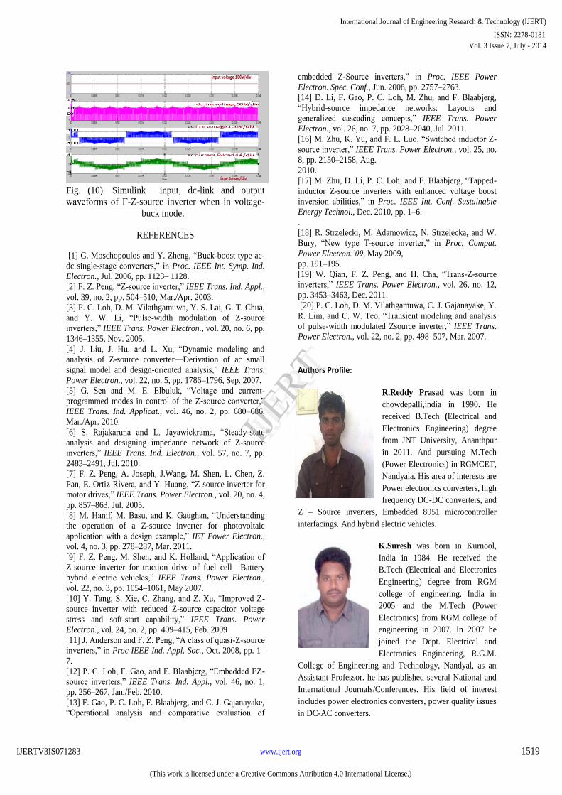
Fig. (10). Simulink input, dc-link and output
waveforms of Г-Z-source inverter when in voltage-
buck mode.
REFERENCES
[1] G. Moschopoulos and Y. Zheng, ―Buck-boost type ac-
dc single-stage converters,‖ in Proc. IEEE Int. Symp. Ind.
Electron., Jul. 2006, pp. 1123– 1128.
[2] F. Z. Peng, ―Z-source inverter,‖ IEEE Trans. Ind. Appl.,
vol. 39, no. 2, pp. 504–510, Mar./Apr. 2003.
[3] P. C. Loh, D. M. Vilathgamuwa, Y. S. Lai, G. T. Chua,
and Y. W. Li, ―Pulse-width modulation of Z-source
inverters,‖ IEEE Trans. Power Electron., vol. 20, no. 6, pp.
1346–1355, Nov. 2005.
[4] J. Liu, J. Hu, and L. Xu, ―Dynamic modeling and
analysis of Z-source converter—Derivation of ac small
signal model and design-oriented analysis,‖ IEEE Trans.
Power Electron., vol. 22, no. 5, pp. 1786–1796, Sep. 2007.
[5] G. Sen and M. E. Elbuluk, ―Voltage and current-
programmed modes in control of the Z-source converter,‖
IEEE Trans. Ind. Applicat., vol. 46, no. 2, pp. 680–686,
Mar./Apr. 2010.
[6] S. Rajakaruna and L. Jayawickrama, ―Steady-state
analysis and designing impedance network of Z-source
inverters,‖ IEEE Trans. Ind. Electron., vol. 57, no. 7, pp.
2483–2491, Jul. 2010.
[7] F. Z. Peng, A. Joseph, J.Wang, M. Shen, L. Chen, Z.
Pan, E. Ortiz-Rivera, and Y. Huang, ―Z-source inverter for
motor drives,‖ IEEE Trans. Power Electron., vol. 20, no. 4,
pp. 857–863, Jul. 2005.
[8] M. Hanif, M. Basu, and K. Gaughan, ―Understanding
the operation of a Z-source inverter for photovoltaic
application with a design example,‖ IET Power Electron.,
vol. 4, no. 3, pp. 278–287, Mar. 2011.
[9] F. Z. Peng, M. Shen, and K. Holland, ―Application of
Z-source inverter for traction drive of fuel cell—Battery
hybrid electric vehicles,‖ IEEE Trans. Power Electron.,
vol. 22, no. 3, pp. 1054–1061, May 2007.
[10] Y. Tang, S. Xie, C. Zhang, and Z. Xu, ―Improved Z-
source inverter with reduced Z-source capacitor voltage
stress and soft-start capability,‖ IEEE Trans. Power
Electron., vol. 24, no. 2, pp. 409–415, Feb. 2009
[11] J. Anderson and F. Z. Peng, ―A class of quasi-Z-source
inverters,‖ in Proc IEEE Ind. Appl. Soc., Oct. 2008, pp. 1–
7.
[12] P. C. Loh, F. Gao, and F. Blaabjerg, ―Embedded EZ-
source inverters,‖ IEEE Trans. Ind. Appl., vol. 46, no. 1,
pp. 256–267, Jan./Feb. 2010.
[13] F. Gao, P. C. Loh, F. Blaabjerg, and C. J. Gajanayake,
―Operational analysis and comparative evaluation of
embedded Z-Source inverters,‖ in Proc. IEEE Power
Electron. Spec. Conf., Jun. 2008, pp. 2757–2763.
[14] D. Li, F. Gao, P. C. Loh, M. Zhu, and F. Blaabjerg,
―Hybrid-source impedance networks: Layouts and
generalized cascading concepts,‖ IEEE Trans. Power
Electron., vol. 26, no. 7, pp. 2028–2040, Jul. 2011.
[16] M. Zhu, K. Yu, and F. L. Luo, ―Switched inductor Z-
source inverter,‖ IEEE Trans. Power Electron., vol. 25, no.
8, pp. 2150–2158, Aug.
2010.
[17] M. Zhu, D. Li, P. C. Loh, and F. Blaabjerg, ―Tapped-
inductor Z-source inverters with enhanced voltage boost
inversion abilities,‖ in Proc. IEEE Int. Conf. Sustainable
Energy Technol., Dec. 2010, pp. 1–6.
.
[18] R. Strzelecki, M. Adamowicz, N. Strzelecka, and W.
Bury, ―New type T-source inverter,‖ in Proc. Compat.
Power Electron.’09, May 2009,
pp. 191–195.
[19] W. Qian, F. Z. Peng, and H. Cha, ―Trans-Z-source
inverters,‖ IEEE Trans. Power Electron., vol. 26, no. 12,
pp. 3453–3463, Dec. 2011.
[20] P. C. Loh, D. M. Vilathgamuwa, C. J. Gajanayake, Y.
R. Lim, and C. W. Teo, ―Transient modeling and analysis
of pulse-width modulated Zsource inverter,‖ IEEE Trans.
Power Electron., vol. 22, no. 2, pp. 498–507, Mar. 2007.
Authors Profile:
R.Reddy Prasad was born in
chowdepalli,india in 1990. He
received B.Tech (Electrical and
Electronics Engineering) degree
from JNT University, Ananthpur
in 2011. And pursuing M.Tech
(Power Electronics) in RGMCET,
Nandyala. His area of interests are
Power electronics converters, high
frequency DC-DC converters, and
Z – Source inverters, Embedded 8051 microcontroller
interfacings. And hybrid electric vehicles.
K.Suresh was born in Kurnool,
India in 1984. He received the
B.Tech (Electrical and Electronics
Engineering) degree from RGM
college of engineering, India in
2005 and the M.Tech (Power
Electronics) from RGM college of
engineering in 2007. In 2007 he
joined the Dept. Electrical and
Electronics Engineering, R.G.M.
College of Engineering and Technology, Nandyal, as an
Assistant Professor. he has published several National and
International Journals/Conferences. His field of interest
includes power electronics converters, power quality issues
in DC-AC converters.
Vol. 3 Issue 7, July - 2014
International Journal of Engineering Research & Technology (IJERT)
IJERT
IJERT
ISSN: 2278-0181
www.ijert.orgIJERTV3IS071283
(This work is licensed under a Creative Commons Attribution 4.0 International License.)
1519