Comp Arch Presentation- DDR4meseec.ce.rit.edu/551-projects/spring2014/2-1.pdfMicrosoft PowerPoint -...
29
DDR4 SDRAM Aaron Pulver & Gregg Miller
Transcript of Comp Arch Presentation- DDR4meseec.ce.rit.edu/551-projects/spring2014/2-1.pdfMicrosoft PowerPoint -...

DDR4 SDRAMAaron Pulver & Gregg Miller

● DRAM Basics● History of DRAM● DDR4 Improvements
o Transfer Rateso Power Consumptiono Memory Size
● Future Outlook
Overview

● Transistor controls trench capacitor
DRAM Basics

1. The row address must be applied to the address pins. The row must be applied for a certain amount of time before /RAS becomes active.
2. /RAS transitions to low.3. The column address is applied to the address pins. The column must be applied for a certain
amount of time before /CAS becomes active but after /RAS becomes inactive. 4. Write enable must be set low for a certain amount of time (tWP).5. Data needs to be applied to the data input pins for before /CAS goes low. 6. /CAS must flip from high to low.7. /CAS and /RAS must return to their inactive states for the cycle to be complete.
DRAM Basic Writing

DRAM Basic Writing

1. The row address has to be sent to the address pins on the memory controller for the correct amount of time before /RAS goes low and held after /RAS goes low.
2. /RAS has to go from high to low and remain low.3. A column address has to be sent to address pins on the memory device for the specified
amount of time and held after /CAS goes low. 4. /WE must be a logical high before /CAS transition. /WE must remain high until after the
transition of /CAS. 5. /CAS has to switch from high to low and remain at a logic 0. 6. /OE must go low. Some systems allow /OE to cycle. /OE can also be tied to ground. 7. Data appears at the output pins. The time when the data appears depends on when /RAS and
/CAS went low and when the address was applied. 8. Finally, /CAS and /RAS must return to their inactive states.
DRAM Basic Reading

DRAM Basic Reading
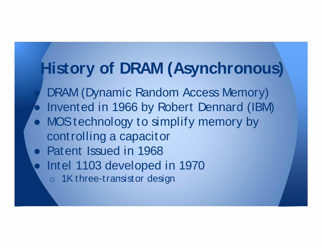
● DRAM (Dynamic Random Access Memory)● Invented in 1966 by Robert Dennard (IBM)● MOS technology to simplify memory by
controlling a capacitor● Patent Issued in 1968● Intel 1103 developed in 1970
o 1K three-transistor design
History of DRAM (Asynchronous)

● Throughout the 70’s & 80’s the density of ram dramatically increased
● New modes to read/writeo Fast Page Modeo Extended Data Outo Other burst type reads
History of DRAM (Asynchronous)
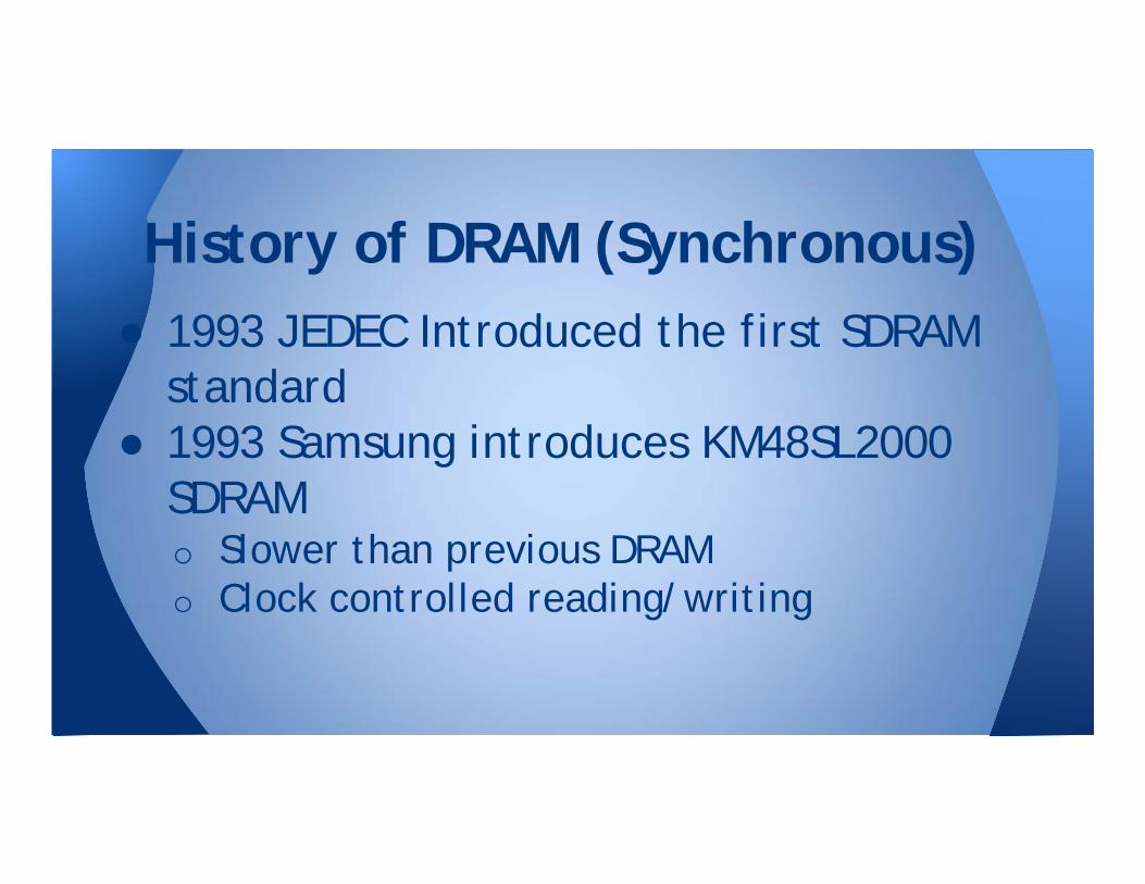
● 1993 JEDEC Introduced the first SDRAM standard
● 1993 Samsung introduces KM48SL2000 SDRAMo Slower than previous DRAM o Clock controlled reading/writing
History of DRAM (Synchronous)

● 2000 JEDEC released DDR (Double Data Rate) Specificationo Rising and falling edge of clocko slower clock frequencies for better signal
integrity
History of DRAM (DDR)

● 2003 The first DDR2 memory module was released
● By the end of 2004, DDR2 was surpassing DDR
History of DRAM (DDR2)

● 2007 DDR3 first introduced● Nearly doubled data transfer rate (up to
2133MT/s)● ~30% less power consumption than DDR2
History of DRAM (DDR3)

● 2005 JEDEC began developing DDR4● Scheduled to reach market by 2012
o Failed to do soo Estimated to reach mass production by end
of 2014
History of DRAM (DDR4)

DRAM Comparison ChartFeature/Option DDR DDR2 DDR3 DDR4 DDR4
Advantage
Voltage (core and I/O)
2.5V-2.6V 1.8V 1.5V 1.2V Reduces memory power demand
Low voltage standard No Yes1.55V
Yes (DDR3L at 1.35V)
Anticipated (likely 1.05V)
Memory power reductions
Data rate (Mb/s) 333, 400, 667, 800 533, 667, 800, 1066 800, 1066, 1333, 1600, 1866, 2133
1600, 1866, 2133, 2400, 2667, 3200
Migration to higher‐speed I/O
Densities 256Mb to 1Gb 256Mb to 4Gb 512Mb–8Gb 2Gb–16Gb Better enablement for large-capacity memory subsystems
Internal banks 4 4 8 16 More banks
Bank groups (BG) 0 0 0 4 Faster burst accesses
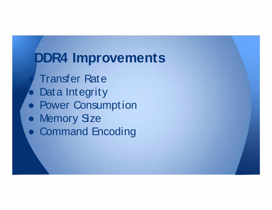
● Transfer Rate● Data Integrity● Power Consumption● Memory Size● Command Encoding
DDR4 Improvements

● Support transfer rates of 2133MT/s up to 3200 MT/s
● Banks and Bank Groups● Point-to-point topology
o Single trace● 284/288 pin DIMM
o NVDIMM
DDR4 Transfer Rate

DDR4 Transfer Rate

● Number of banks is increased from 8 to 16● DDR4 SDRAM architecture uses 8n prefetch with bank groups. This includes two or four
selectable bank groups. This enables the DDR4 SDRAM to have separate activation, read, write or refresh operations underway in each of the unique bank groups. This techniques increases the memory bandwidth and efficiency. It is particularly suited for memory applications where small levels of granularity are required.
DDR4 Transfer Rate
Banks and Bank Groups

● There will no longer be a shared data bus for every 2 DIMMs.
● Each DIMM will now have it’s own data bus.
DDR4 Data Transfer Rate
Point-to-Point Topology
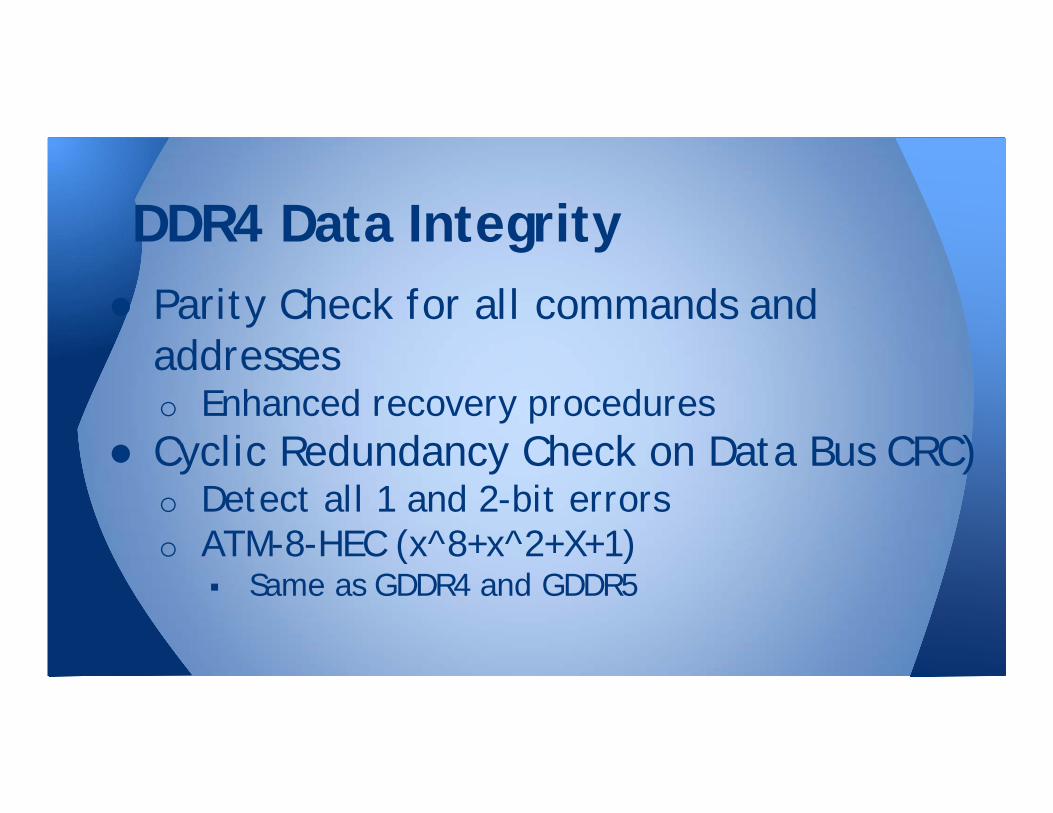
● Parity Check for all commands and addresseso Enhanced recovery procedures
● Cyclic Redundancy Check on Data Bus CRC)o Detect all 1 and 2-bit errorso ATM-8-HEC (x^8+x^2+X+1)
Same as GDDR4 and GDDR5
DDR4 Data Integrity

● Lower Voltage Requirement (1.2V)● Data Bus Inversion● Pseudo Open Drain
DDR4 Power

● Limit transistor switching by inverting/not inverting datao Extra bit added to data to signify inversion
● DBI-DCo Minimize number of ones/zeros transmitted
● DBI-ACo Compare current data with previous data
DDR4 Power
DDR4 Data Bus Inversion (DBI)

DDR4 Power
DDR4 Data Bus Inversion (DBI)

DDR4 Power
Pseudo Open Drain

● Die Stackingo Reduced load(power)o Smaller footprint
● Smaller technology
DDR4 Capacity

New /ACT bit to replace old /RAS=L, /CAS=H, /WE=H combination and have larger row address range.
DDR4 Capacity
DDR4 Command Changes

● Follows similar path while still viableo Increased speedo Higher densityo Lower voltage
More focus here in coming future as mobile device market increases
Future of Memory(DDR5?)

Questions?