COMMUNICATION SYNTHESIS OF NETWORKS-ON-CHIP (NoC) A ...
123
COMMUNICATION SYNTHESIS OF NETWORKS-ON-CHIP (NoC) A Dissertation by PRAVEEN SUNDER BHOJWANI Submitted to the Office of Graduate Studies of Texas A&M University in partial fulfillment of the requirements for the degree of DOCTOR OF PHILOSOPHY December 2007 Major Subject: Computer Engineering
Transcript of COMMUNICATION SYNTHESIS OF NETWORKS-ON-CHIP (NoC) A ...

COMMUNICATION SYNTHESIS OF NETWORKS-ON-CHIP (NoC)
A Dissertation
by
PRAVEEN SUNDER BHOJWANI
Submitted to the Office of Graduate Studies ofTexas A&M University
in partial fulfillment of the requirements for the degree of
DOCTOR OF PHILOSOPHY
December 2007
Major Subject: Computer Engineering

COMMUNICATION SYNTHESIS OF NETWORKS-ON-CHIP (NoC)
A Dissertation
by
PRAVEEN SUNDER BHOJWANI
Submitted to the Office of Graduate Studies ofTexas A&M University
in partial fulfillment of the requirements for the degree of
DOCTOR OF PHILOSOPHY
Approved by:
Chair of Committee, Rabi N. MahapatraCommittee Members, Duncan M. Walker
Eun J. KimGwan Choi
Head of Department, Valerie E. Taylor
December 2007
Major Subject: Computer Engineering

iii
ABSTRACT
Communication Synthesis of Networks-on-Chip (NoC). (December 2007)
Praveen Sunder Bhojwani, B.Tech.(H), Indian Institute of Technology (IIT),
Kharagpur;
M.S., Texas A&M University;
Chair of Advisory Committee: Rabi N. Mahapatra
The emergence of networks-on-chip (NoC) as the communication infrastructure solu-
tion for complex multi-core SoCs presents communication synthesis challenges. This
dissertation addresses the design and run-time management aspects of communica-
tion synthesis. Design reuse and the infeasibility of Intellectual Property (IP) core
interface redesign, requires the development of a Core-Network Interface (CNI) which
allows them to communicate over the on-chip network. The absence of intelligence
amongst the NoC components, entails the introduction of a CNI capable of not only
providing basic packetization and depacketization, but also other essential services
such as reliability, power management, reconfiguration and test support. A generic
CNI architecture providing these services for NoCs is proposed and evaluated in this
dissertation.
Rising on-chip communication power costs and reliability concerns due to these,
motivate the development of a peak power management technique that is both scal-
able to different NoCs and adaptable to varying traffic configurations. A scalable
and adaptable peak power management technique - SAPP - is proposed and demon-
strated. Latency and throughput improvements observed with SAPP demonstrate its
superiority over existing techniques.
Increasing design complexity make prediction of design lifetimes difficult. Post

iv
SoC deployment, an on-line health monitoring scheme, is essential to maintain con-
fidence in the correct operation of on-chip cores. The rising design complexity and
IP core test costs makes non-concurrent testing of the IP cores infeasible. An on-line
scheme capable of managing IP core test in the presence of executing applications is
essential. Such a scheme ensures application performance and system power budgets
are efficiently managed. This dissertation proposes Concurrent On-Line Test (COLT)
for NoC-based systems and demonstrates how a robust implementation of COLT us-
ing a Test Infrastructure-IP (TI-IP) can be used to maintain confidence in the correct
operation of the SoC.

v
To my family

vi
ACKNOWLEDGMENTS
I would like to thank Dr. Mahapatra for his direction and support over the
last six years. His faith in my abilities helped mould my transition from a graduate
student into a researcher. I would also like to thank Drs. Walker, Kim and Choi for
serving on my committee and being excellent teachers.
Over the last six years, a number of colleagues and friends have made my stay
in College Station bearable. I would like to thank Sunil, Pramod, Sid, Kiran, Junyi,
Anand, Kabi, Purna, Nitesh, Tae Sung, Di, Rupak, Veera, Rohit, Waqar, Prasenjit,
Sarabjyot, Anuja, Upali, Jason, Suman, Nikhil, Amar, Nari, Vivek, Pandi, Praveen,
Abhijit, Narayanan, Binoy and my wing-mates.
The support of my family over the last six years has been instrumental in the
compilation of this dissertation.

vii
TABLE OF CONTENTS
CHAPTER Page
I INTRODUCTION . . . . . . . . . . . . . . . . . . . . . . . . . . 1
II CORE-NETWORK INTERFACE DESIGN . . . . . . . . . . . . 7
A. Related Work . . . . . . . . . . . . . . . . . . . . . . . . . 8
B. Proposed CNI Design . . . . . . . . . . . . . . . . . . . . . 8
1. CNI Services . . . . . . . . . . . . . . . . . . . . . . . 8
a. End-to-end Reliable Communication . . . . . . . 9
b. Communication Scheduling . . . . . . . . . . . . 9
c. Peak Power Management and Network Recon-
figurability . . . . . . . . . . . . . . . . . . . . . . 10
d. IP Core Test Support . . . . . . . . . . . . . . . . 10
2. CNI Architectural Sub-components . . . . . . . . . . . 11
C. Latency Constrained On-chip Communication . . . . . . . 15
1. Factors Affecting End-to-end Latency . . . . . . . . . 15
2. Proposed VC Allocation Scheme . . . . . . . . . . . . 16
3. VCA Architecture . . . . . . . . . . . . . . . . . . . . 17
4. NoC Support . . . . . . . . . . . . . . . . . . . . . . . 17
5. Setting the Class id Field . . . . . . . . . . . . . . . . 18
6. Evaluating Class-based VCA . . . . . . . . . . . . . . 19
D. CNI Evaluation . . . . . . . . . . . . . . . . . . . . . . . . 20
E. Unconsidered Design Issues . . . . . . . . . . . . . . . . . 22
III PEAK POWER AWARE NOCS . . . . . . . . . . . . . . . . . . 23
A. Related Work . . . . . . . . . . . . . . . . . . . . . . . . . 24
1. Energy/Power Model . . . . . . . . . . . . . . . . . . 24
2. PowerHerd . . . . . . . . . . . . . . . . . . . . . . . . 25
3. Peak Power Control (PC) . . . . . . . . . . . . . . . . 27
B. Static Peak Power Aware Design . . . . . . . . . . . . . . 27
1. Problem Formulation . . . . . . . . . . . . . . . . . . 28
2. Definitions and Operations . . . . . . . . . . . . . . . 30
3. Heuristic . . . . . . . . . . . . . . . . . . . . . . . . . 31
4. Off-line Peak Power Control . . . . . . . . . . . . . . . 33
5. Evaluation . . . . . . . . . . . . . . . . . . . . . . . . 34

viii
CHAPTER Page
C. SAPP: Scalable and Adaptable Peak Power Manage-
ment in NoCs . . . . . . . . . . . . . . . . . . . . . . . . . 37
1. SAPP . . . . . . . . . . . . . . . . . . . . . . . . . . . 38
a. Flit Injection Control . . . . . . . . . . . . . . . . 38
b. Peak Power Budget Re-allocation . . . . . . . . . 39
c. Budget Re-allocation Check-pointing . . . . . . . 41
2. Feature Comparison with Other Schemes . . . . . . . 42
3. Experimental Setup and Results . . . . . . . . . . . . 43
a. Test Cases . . . . . . . . . . . . . . . . . . . . . . 43
b. Performance Evaluation . . . . . . . . . . . . . . 44
IV CONCURRENT ON-LINE TESTING . . . . . . . . . . . . . . 50
A. Related Work . . . . . . . . . . . . . . . . . . . . . . . . . 51
1. Off-line Testing . . . . . . . . . . . . . . . . . . . . . . 51
2. On-line Testing . . . . . . . . . . . . . . . . . . . . . . 52
B. Challenges to COLT . . . . . . . . . . . . . . . . . . . . . 52
C. Test Infrastructure-IP Design . . . . . . . . . . . . . . . . 53
1. TI-IP Components . . . . . . . . . . . . . . . . . . . . 55
2. TI-IP Operation . . . . . . . . . . . . . . . . . . . . . 56
3. Multi TI-IP Operation . . . . . . . . . . . . . . . . . . 60
D. Robust Protocol for COLT . . . . . . . . . . . . . . . . . . 62
1. Protocol Specification . . . . . . . . . . . . . . . . . . 62
2. Protocol Hazards . . . . . . . . . . . . . . . . . . . . . 66
3. Hazard Mitigation . . . . . . . . . . . . . . . . . . . . 68
E. Experimental Setup and Results . . . . . . . . . . . . . . . 70
1. NoCSim Modification . . . . . . . . . . . . . . . . . . 70
2. ITC’02 SoC Test Benchmark . . . . . . . . . . . . . . 70
3. Embedded Systems Synthesis Benchmark Suite . . . . 71
4. Test Configurations . . . . . . . . . . . . . . . . . . . 71
5. TI-IP Validation . . . . . . . . . . . . . . . . . . . . . 73
a. SoC Configuration 1 . . . . . . . . . . . . . . . . 73
b. SoC Configuration 2 . . . . . . . . . . . . . . . . 76
6. Robust Protocol Validation . . . . . . . . . . . . . . . 78
7. Synthesis Results . . . . . . . . . . . . . . . . . . . . . 78
V SUMMARY . . . . . . . . . . . . . . . . . . . . . . . . . . . . . 81
A. Conclusions . . . . . . . . . . . . . . . . . . . . . . . . . . 81
B. Future Work . . . . . . . . . . . . . . . . . . . . . . . . . . 82

ix
Page
REFERENCES . . . . . . . . . . . . . . . . . . . . . . . . . . . . . . . . . . . 84
APPENDIX A FORWARD ERROR CORRECTION IN NOCS . . . . . . . 93
A. Introduction . . . . . . . . . . . . . . . . . . . . . . . . . . 93
B. Related Work . . . . . . . . . . . . . . . . . . . . . . . . . 95
1. FEC Basics . . . . . . . . . . . . . . . . . . . . . . . . 95
2. Energy Model . . . . . . . . . . . . . . . . . . . . . . 96
C. Motivation . . . . . . . . . . . . . . . . . . . . . . . . . . . 97
D. On-chip Communication Reliability . . . . . . . . . . . . . 100
1. Error Detection and Retransmission (ED+R) . . . . . 100
a. End-to-end Retransmission . . . . . . . . . . . . . 101
b. Hop-to-hop Retransmission . . . . . . . . . . . . 102
2. Forward Error Correction (FEC+R) . . . . . . . . . . 104
3. Hybrid Scheme (FEC/ED+R) . . . . . . . . . . . . . 105
E. Conclusions . . . . . . . . . . . . . . . . . . . . . . . . . . 108
APPENDIX B NOCSIM . . . . . . . . . . . . . . . . . . . . . . . . . . . . . 109
VITA . . . . . . . . . . . . . . . . . . . . . . . . . . . . . . . . . . . . . . . . 110
x
LIST OF TABLES
TABLE Page
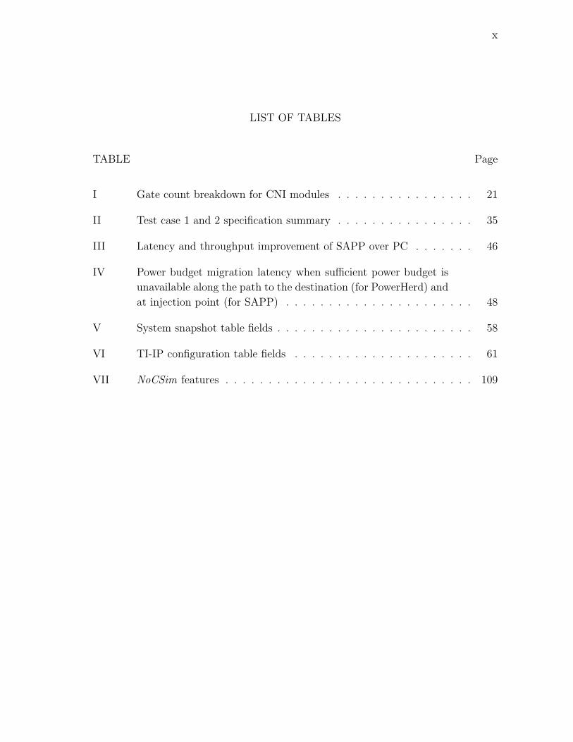
I Gate count breakdown for CNI modules . . . . . . . . . . . . . . . . 21
II Test case 1 and 2 specification summary . . . . . . . . . . . . . . . . 35
III Latency and throughput improvement of SAPP over PC . . . . . . . 46
IV Power budget migration latency when sufficient power budget is
unavailable along the path to the destination (for PowerHerd) and
at injection point (for SAPP) . . . . . . . . . . . . . . . . . . . . . . 48
V System snapshot table fields . . . . . . . . . . . . . . . . . . . . . . . 58
VI TI-IP configuration table fields . . . . . . . . . . . . . . . . . . . . . 61
VII NoCSim features . . . . . . . . . . . . . . . . . . . . . . . . . . . . . 109

xi
LIST OF FIGURES
FIGURE Page
1 NoC architecture . . . . . . . . . . . . . . . . . . . . . . . . . . . . . 2
2 NoC design process illustrating off-line and on-line steps . . . . . . . 4
3 Core-Network Interface architecture . . . . . . . . . . . . . . . . . . 11
4 Application data is sent over the NoC in the form of packets,
which are further broken up into flits . . . . . . . . . . . . . . . . . . 13
5 On-chip router internals . . . . . . . . . . . . . . . . . . . . . . . . . 16
6 Simplified architecture for class-based VCA . . . . . . . . . . . . . . 18
7 Latency vs hop distance for varying classes . . . . . . . . . . . . . . . 19
8 Effective MIPS for processor for different cache miss rates . . . . . . 20
9 Taxonomy of peak power management techniques for NoCs . . . . . 24
10 Energy distribution profile for different loads . . . . . . . . . . . . . . 26
11 (a) MCG, (b) NCG, (c) NCG after merge operation . . . . . . . . . . 29
12 Test case 1: Peak power results for different NoC configurations
(Peak power constraint = 1.5W) . . . . . . . . . . . . . . . . . . . . 35
13 Test case 1: Effect of peak power control on NoC throughput . . . . 36
14 Test case 2: Peak power results for different NoC configurations
(Peak power constraint = 0.35W) . . . . . . . . . . . . . . . . . . . . 36
15 Test case 2: Average flit latency . . . . . . . . . . . . . . . . . . . . . 37
16 Two snapshots of peak power budget re-allocation in NoC . . . . . . 40
17 Non-uniform test configurations . . . . . . . . . . . . . . . . . . . . . 45
xii
FIGURE Page
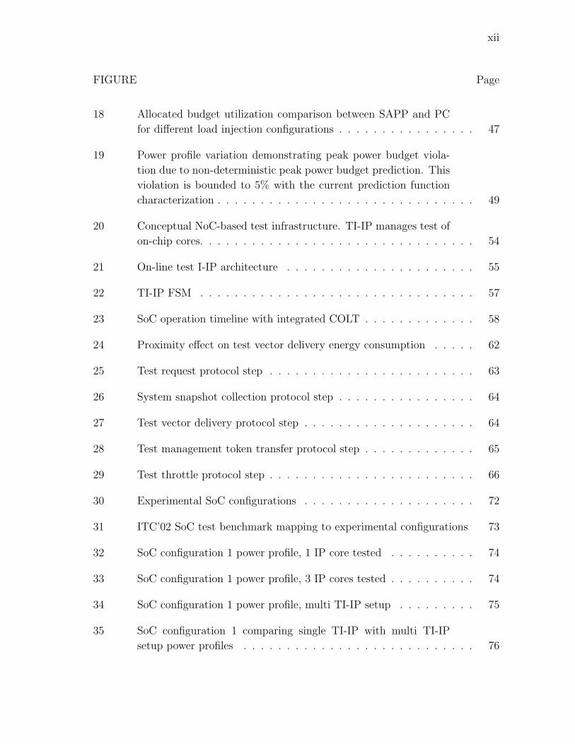
18 Allocated budget utilization comparison between SAPP and PC
for different load injection configurations . . . . . . . . . . . . . . . . 47
19 Power profile variation demonstrating peak power budget viola-
tion due to non-deterministic peak power budget prediction. This
violation is bounded to 5% with the current prediction function
characterization . . . . . . . . . . . . . . . . . . . . . . . . . . . . . . 49
20 Conceptual NoC-based test infrastructure. TI-IP manages test of
on-chip cores. . . . . . . . . . . . . . . . . . . . . . . . . . . . . . . . 54
21 On-line test I-IP architecture . . . . . . . . . . . . . . . . . . . . . . 55
22 TI-IP FSM . . . . . . . . . . . . . . . . . . . . . . . . . . . . . . . . 57
23 SoC operation timeline with integrated COLT . . . . . . . . . . . . . 58
24 Proximity effect on test vector delivery energy consumption . . . . . 62
25 Test request protocol step . . . . . . . . . . . . . . . . . . . . . . . . 63
26 System snapshot collection protocol step . . . . . . . . . . . . . . . . 64
27 Test vector delivery protocol step . . . . . . . . . . . . . . . . . . . . 64
28 Test management token transfer protocol step . . . . . . . . . . . . . 65
29 Test throttle protocol step . . . . . . . . . . . . . . . . . . . . . . . . 66
30 Experimental SoC configurations . . . . . . . . . . . . . . . . . . . . 72
31 ITC’02 SoC test benchmark mapping to experimental configurations 73
32 SoC configuration 1 power profile, 1 IP core tested . . . . . . . . . . 74
33 SoC configuration 1 power profile, 3 IP cores tested . . . . . . . . . . 74
34 SoC configuration 1 power profile, multi TI-IP setup . . . . . . . . . 75
35 SoC configuration 1 comparing single TI-IP with multi TI-IP
setup power profiles . . . . . . . . . . . . . . . . . . . . . . . . . . . 76

xiii
FIGURE Page
36 SoC configuration 2 power profile, single TI-IP setup . . . . . . . . . 77
37 SoC configuration 2 multi TI-IP setup power profile . . . . . . . . . . 78
38 SoC configuration 2 single TI-IP vs multi TI-IP power profile . . . . 78
39 Energy profile demonstrating starvation hazard mitigation . . . . . . 79
40 Energy profile demonstrating TI-IP test throttling effect on mis-
behaving application . . . . . . . . . . . . . . . . . . . . . . . . . . . 79
41 Motivation behind selecting target FER for FEC module: Energy
vs FER at varying hop lengths . . . . . . . . . . . . . . . . . . . . . 98
42 Motivation behind selecting target FER for FEC module: Average
Flit latency vs FER at varying hop lengths . . . . . . . . . . . . . . 98
43 Error rate vs signal to noise ratio for varying LDPC iterations . . . . 99
44 CNI structure . . . . . . . . . . . . . . . . . . . . . . . . . . . . . . . 101
45 Average flit latency for end-to-end vs hop-to-hop reliability (CRC) . 103
46 Energy for hop-to-hop vs end-to-end reliability . . . . . . . . . . . . 103
47 Energy of ED+R and FEC+R vs hop length for varying FERs . . . . 106
48 Average flit latency for ED+R and FEC+R vs hop length at vary-
ing FERs . . . . . . . . . . . . . . . . . . . . . . . . . . . . . . . . . 106
49 Flit fields/overheads for different schemes . . . . . . . . . . . . . . . 107

1
CHAPTER I
INTRODUCTION
In 1965, Gordon E. Moore predicted that the number of transistors on a chip would
double every two years [1]. Technology improvements have allowed for this prediction
to hold true for over four decades, allowing for density to almost double every 18
months. The International Technology Roadmap for Semiconductors (ITRS) indi-
cates that these trends will continue till atleast the end of the decade, allowing for
more than a billion transistors on a chip [2].
This technology scaling trend allows for the design of complex multi-core systems-
on-a-chip (SoC). These SoCs will be capable of executing multiple applications pro-
viding a wide variety of features. Early SoC designs utilized bus-based communication
infrastructures for interactions between the Intellectual Property (IP) cores. In 2000,
Guerrier and Greiner identified that as designs got more complex and applications
became communication intensive, bus-based infrastructures would no longer be suf-
ficient [3]. They proposed the use of on-chip packet-switched networks to address
contention, scalability and availability concerns. This idea was also reiterated by
Towles and Dally, in the form of an abstract design of a SoC utilizing a folded 2D
torus packet-switched network and a regular IP core layout [4]. In research litera-
ture, these on-chip networks are referred to as Networks-on-Chip (NoC). Figure 1
illustrates an architecture considered by most NoC researchers. This architecture
consists of a regular layout of network tiles. These tiles consist of IP cores interfaced
with NoCs via core-network interfaces (CNI). On-chip routers route communication
between the source and destination network tiles, over links between them. A pro-
The journal model is IEEE Transactions on Automatic Control.

2
tocol stack similar to the one used in wide-area networks has also been proposed for
the on-chip network environment [5].
Fig. 1. NoC architecture
Communication synthesis of NoCs involves the design of components required
for on-chip communication and the necessary support for its run-time management.
Design aspects for NoCs cover challenges such as application mapping, topology se-
lection and NoC synthesis. Application mapping determines mapping of application
task graphs to processing elements in the SoC. This mapping is typically constrained
by execution time budgets and deadlines. This idea is pretty similar to the traditional
hardware/software partitioning [6], with the exception that communication between
the IP cores is no longer trivial. In [7], the authors proposed energy constrained
mapping of task graphs to processors, setting communication routes based on band-
width constraints. An energy aware mapping and routing technique was also proposed
in [8]. To improve on algorithm run-time, the research in [9] proposed a heuristic to
determine the neighborhood for communicating cores in a regular NoC, while schedul-
ing communication on the network links to ensure performance constraints are met.
Topology exploration and selection techniques were proposed in [10, 11, 12]. A number
of NoC sythesis techniques using heuristics and optimization algorithms have been
proposed in [12, 13, 14, 15], allowing for the design of application specific NoCs.
Run-time management of NoCs considers issues such as peak power control,

3
hotspot avoidance, communication reliability and on-chip core health. These present
critical challenges to the reliable operation of the SoC. Peak power management has
an impact on design reliability and the cooling costs associated with the system.
Techniques to address this challenge have been proposed in [16, 17]. By controlling
communication flow in the NoC, these techniques manage power consumption. Pro-
viding reliability in on-chip networks were explored in [18, 19, 20]. The first efforts
at looking into the on-line health management for SoCs have been addressed in this
dissertation [21, 22]. Figure 2 illusrates how these design challenges fit into a NoC-
based system complete design process, identifying challenges to be addressed design
time and run-time. The steps in bold have been researched in this dissertation.
This dissertation makes three novel contributions in both aspects of communica-
tion synthesis for NoC-based systems. The primary contribution is in the domain of
Core-Network Interfacing. In the IP reuse design space, providing for an interface to
NoCs is an essential design step. Apart from allowing the IP core to talk the language
of the network, this dissertation identifies other services that may be provided by the
Core-Network Interface (CNI) - reliable communication, peak power management,
IP core test support and NoC reconfiguration. A generic architecture that can be
customized to varying IP core interfaces and NoC configurations is also proposed.
An evaluation of the costs associated with the CNI is reported, demonstrating the
feasibility of the proposed design.
Peak power management in NoCs is a design concern that can be addressed in
different ways. This dissertation examines peak power management at (i) design
time (static) and (ii) run-time (dynamic). Design time approaches lead to pesimisstic
solutions that impact performance. Dynamic approaches allow for adaptive solutions
to address these performance concerns, but are limited by available compute resources
to aid in the peak power management for NoCs. A Scalable, Adaptable Peak Power

4
Fig. 2. NoC design process illustrating off-line and on-line steps

5
(SAPP) management technique is proposed in this dissertation to address scalability
and adaptability limitations of previously proposed techniques.
Lifetime reliability challenges presented by complex multi-core SoCs require the
deployment of an on-line health monitoring technique to track the health of the on-
chip cores. Post SoC deployment, confidence in the health of on-chip cores can be
obtained by performing IP core test using existing test support. This would typically
be performed non-concurrently, i.e. by turning off executing applications. But with
rising design complexity and test costs - test time and test power - non-concurrent
testing is not feasible. Concurrent test of IP cores in presence of executing applications
in the system is essential. NoC components can facilitate this process, with the help
of an infrastructure-IP (I-IP). This dissertation proposes the deployment of a Test
Infrastructure-IP (TI-IP) into a NoC-based SoC, to provide Concurrent On-Line Test
(COLT) support for the on-chip components. The challenges to COLT are identified
and addressed by the proposed TI-IP design. A robust protocol of operation is also
documented along with implementation costs.
This dissertation is organized as follows: Chapter II discusses the Core-Network
Interfacing issues and proposes the essential CNI service set and support architec-
ture required for efficient and reliable operation of NoCs. Performance support from
on-chip routers in the form of class-based virtual channel allocation is also discussed
with results demonstrating their effectiveness. Chapter III proposes a novel peak
power management techniques for NoCs, while addressing the scalability and adapt-
ability limitations of prior research attempts. Evaluation highlighting the observed
improvements are also reported. Chapter IV motivates the need for a concurrent on-
line health monitoring system for SoCs. Challenges to the proposed technique COLT
are documented and solutions are deployed using a a robust TI-IP implementation.
Performance on different SoC configuration prepared using academic benchmarks are

6
reported to establish the feasibility of deploying COLT. Finally, the dissertation is
summarized in the last chapter, and a few concluding remarks on future work are
presented.
Note: Since this dissertation does not investigate design exploration strategies
for NoC-based system designs, a single baseline NoC configuration is assumed and
configured into the evaluation platform NoCSim. This platform is configured for a
2D folded torus 4x4 layout of IP cores in an SoC. Source routing is used to route
communication between network tiles, while virtual channel based flow control is
utilized to avoid communication blocking.
Concepts proposed in this dissertation are implemented into NoCSim for func-
tional validation. Appendix B lists the features of this evalutation platform.

7
CHAPTER II
CORE-NETWORK INTERFACE DESIGN
In light of rising shorter time-to-market (TTM) pressures and design reuse, inter-
facing pre-existing IP cores to formulate complex multi-core SoCs presents a critical
design challenge. When designing NoC-based systems, modifying core interfaces to
communicate over a NoC is not feasible and sometimes impossible. The interface
protocols and specifications are extensively pre-verified and validated, and may not
have been designed with the intent for deployment in NoCs.
These interfaces can broadly be classified into two categories: (i) standard inter-
faces and (ii) non-standard (or in-house) interfaces. Standard interfaces like the Open
Core Protocol - International Partnership (OCP-IP) [23], VSI Alliance (VSIA) [24]
and Advanced Microcontroller Bus Architecture (AMBA) family of interfaces [25] are
widely used in present day system designs. Their interface specifications are well-
defined and widely available in the public domain or by membership. Non-standard
interfaces are usually propietary to a corporation and used to design SoCs with IP
cores from a single library or vendor.
To integrate IP cores with this variety of possible interfaces, an adapter is re-
quired to translate signals from the IP core domain into signals in the NoC domain
and back again. This translation would be provided in the form of a packetization and
depacketization functionality, thus allowing for communication over the NoC. Besides
these services, this dissertation proposes a set of essential services to be provided by
the CNI to manage the NoC operation. The following sections discuss related research
and present the proposed services and a generic CNI architecture that can be applied
to any IP core interface and NoC configuration, by configuring specific blocks of the
design, thus avoiding complete redesign of the CNI.

8
A. Related Work
The first research [9, 26] addressing the interfacing aspects in NoCs, compared costs
(area and performance) of providing packetization in software, hardware and with a
co-processor attached to a Xtensa core [27]. The software implementation provided an
API for the programmer to send data over the IP core interface in a packetized form.
The hardware implementation utilized a hardware adapter that packetized interface
signals. The co-processor based implementation added a special instruction to the
Xtensa processor Instruction Set Architecture (ISA) using the Tensilica Instruction
Extension (TIE) language. Other NoC research limit interface service to packetization
and de-packetization. This dissertation proposes a generic, enhanced CNI architecture
design that provides services required for the reliable and efficient operation of NoCs.
Concurrent research efforts documented in [28] identified a similiar service set essential
for NoCs.
B. Proposed CNI Design
The CNI design is specified in terms of its services and architecture. The following
subsections detail the proposed service set and generic CNI architecture.
1. CNI Services
The purpose of the CNI is to provide an interface for the IP cores to the NoC. Apart
from packetization and de-packetization functionality, it would also provide: end-to-
end reliability, communication scheduling, NoC reconfigurability, power management
and testing of IP cores.

9
a. End-to-end Reliable Communication
With reducing noise margins in current and future SoC designs, data communication
in on-chip networks are susceptible to errors and schemes to recover from these need
to be incorporated into the NoC. In a multi-hop NoC, these schemes can either be
used in a hop-to-hop or end-to-end fashion. Deciding between these will depend on
the error rates of the design. If reliability concerns warrant the use of end-to-end
reliability, these schemes would be implemented within the CNI. Appendix A reports
on some of the studies performed in this regard. Error detecting codes such as CRC
and hamming have been previously suggested to detect errors and request retransmis-
sions [20, 29]. Forward error correction (FEC) can also be used to reduce the number
of retransmissions, especially if the power and latency costs associated with them are
unacceptable. Previous research have examined the feasibility of using a scaled down
low density parity check coders (LDPC) [30] for use in on-chip networks [19].
b. Communication Scheduling
With SoCs being proposed for use in real-time (RT) systems, it places timing con-
straints on all operational aspects of the system. These not only apply to the com-
putational components of the system, but also the communication infrastructure.
Providing latency constraints to on-chip communications will be essential for correct
operation of the system. Since the CNIs control the communication entering the NoC,
they are in the ideal position to provide for communication scheduling. Schemes pre-
viously used in distributed embedded systems may not be feasible for use in cost
constrained NoCs where a simple, yet effective scheme is needed. Support for such a
scheme would also be needed from the NoC. We utilize the proposed class-based VC
allocation scheme which is supported by the router discussed in Section C.

10
c. Peak Power Management and Network Reconfigurability
Network reconfigurability is essential in dynamic systems. With changing commu-
nication requirements, certain aspects, such as flit routes and stream bandwidth
allocation may need to be modified at runtime. In the NoC configuration consid-
ered, we use source routing, which requires a route table to provide the flit with the
route to the destination. Routes within a dynamic system may need to be changed
to accommodate avoidance of hotspots that may lead to system failure and latency
violations. In [31], the authors used a static bandwidth allocation scheme when VC
based communication was used. Since the power consumption in the NoC is directly
proportional to the bandwidth of the communication on-chip, the bandwidth allo-
cation may need to be scaled to manage power and control propagation latency to
the destination. Scaling of bandwidth is implemented in the CNI itself and may be
implemented in the routers, but this will lead to buffering issues at the intermediate
nodes in the NoC. This dissertation also proposes a dynamic peak power manage-
ment technique to address any limitations of off-line techniques. Chapter III details
the proposed schemes for peak power management in NoCs and compares them to
existing techniques.
The CNI can also be reconfigured based on events monitored in the NoC. [32]
introduced the monitoring service for NoCs. Events monitored can be provided to
the relevant CNIs in the system to allow for reconfiguration.
d. IP Core Test Support
Another functionality for the CNI is that of testing of the IP cores attached to it.
Prior research [33] has indicated the possibility of reusing the NoC as a Test Access
Mechanism (TAM). Since test requests and responses need to be properly interfaced,

11
by providing a test controller, we believe that the testability of the SoC can be
managed more effectively. The Concurrent On-Line Test technique proposed in this
dissertation (see Chapter IV) utilizes the test controller to interface test with the IP
core.
2. CNI Architectural Sub-components
An architectural sketch of the proposed CNI is shown in Figure 3 below. It high-
lights the major components. To provide the essential CNI services, the following
Fig. 3. Core-Network Interface architecture
sub-components are integrated into the proposed architecture.
IP Interface Arbiter: The arbiter behaves as a proxy for communication between
the IP cores attached to the NoC. It accepts (delivers) communication requests (re-
sponses) to the various IP cores. It replays the communication protocols associated
with the core interface standard. A FSM representing the protocol is be used to
configure the arbiter. For this research we have considered the OCP-IP 2.0 interface
specification and have developed an arbiter capable of interfacing with the basic signal

12
set of the OCP interface. Actual implementations and protocols cannot be specified
here due to privacy considerations. The arbiter tracks communication requests from
multiple cores attached to it via the state table.
Encoder/Decoder: The coders are used to provide for end-to-end reliability. Data
to be transmitted is encoded at the sender CNI, transmitted over the NoC to the
receiver CNI where it is decoded. The decoder either detects or corrects errors in the
transmitted data based on the selected coding scheme. The ”strength” of the coding
scheme depends on the desired level of reliability and the acceptable cost of imple-
mentation in terms of silicon area, power and latency. In the presence of multiple
coders in the CNI, varying levels of strengths maybe supported based on the detected
error rates in the system. The CNIC would be responsible for the selection amongst
multiple schemes based on observed error rates.
Packetizer/De-packetizer: Data to be sent over the NoC is sent in the form of
packets. These packets are further broken up into flits (flow digits), which are the
smallest atomic data chunks sent over the NoCs. The flits are limited by their size,
hence a single packet of data is made up of multiple flits. Each packet larger than a
single flit in size, contains a HEAD flit and TAIL flit. Packets larger than two flits
in size also have DATA flits, which contain application data. Figure4 illustrates the
data fragmentation.
As mentioned in [26], the main functionality of the packetizer is to prepare the
flits to be sent out over the NoC. It packetizes the encoded data and sets all the
fields of the flit. The de-packetizer accepts flits from the NoC and forwards them to
the decoder before delivery to the target IP core. The NoC parameters that affect
the packetizer configuration are: topology, routing, flow control policy, VC allocation
scheme, etc.
Route Table (RT): The RT provides for address translation between the IP core

13
Fig. 4. Application data is sent over the NoC in the form of packets, which are further
broken up into flits
and the NoC addressing. It maps addresses issued by the IP cores into routes to
the intended destinations (i.e. host intelligent routing). When responses are to be
returned, the query is made in the form of network addresses. The network address
consists of the network tile ID and the IP core ID that will be assigned at design time.
When requests are packetized, the source id field of the flit is set with the network
address of the sending CNI.
When router intelligent routing is used in the NoC, the DT/RT will provide the
network address of the destination IP core. This address will be looked up in the RT
at the intermediate hops in the NoC.
CNI Controller (CNIC): The CNIC manages the operation of the CNI and con-
trols its sub-components. Since the CNI is pipelined (5 stages), CNIC manages control
signals for each of the pipelined stages. When reconfigurability is supported by the
CNI, the CNIC will be responsible for updating the sub-components like CNI-CS and
DT/RT. Connected to the ST, the CNIC assigns and records stream IDs to com-
munications originating from the network tile. When issuing responses, it provides
the packetizer with stream ID from the received request flit. On the receipt of a
response, the stream ID entry is removed from the ST, allowing it to be reused on

14
future outgoing requests.
CNI Communication Scheduler (CNI-CS): The CNICS provides initial VC al-
location to the flit emerging from the CNI. It does so based on the requested VC
allocation class. Details on class-based VC allocation scheme, its benefits and setting
of the class id field of the flit are discussed in Section C. When supporting dynamic
bandwidth scaling, the CNICS is responsible for modifying the bandwidth allocated
to the communication streams originating from this CNI. The bandwidth allocations
are modified by the CNIC.
Link Controller (LC): It provides an interface for the CNI to the NoC. Its purpose
is to match CNI operation parameters like clock rate to that of the NoC. In cases
where clock rates do not match, additional buffers may be needed to match the arrival
and service rates of the CNI and NoC.
Power Manager (CNI-PM): Most IP cores are capable of operating in low power
modes. When determination of the operating mode is dependent on the communica-
tion characteristics, the CNI-PM will be used to manage the states of operation. The
CNI-PM also manage NoC power. Since power consumption in the NoC is depen-
dent on the volume of traffic, managing traffic injection into the NoC control power
consumption. Chapter III details the investigation performed on this aspect.
Test Controller (TC): The TC handles testing of the IP cores through available IP
test interfaces. It may either receive test vectors from remote network tiles or obtain
them from a local test memory. Results from the TC can be utilized in reconfigur-
ing the NoC too. In the current implementation of the CNI, we do not include the
CNI-PM and TC since these are dependent on the IP core characteristics.
Some sub-components of the CNI are IP core specific, while others are NoC
specific. The interface arbiter is IP core interface specific and is configured to replay
the interface protocol. The packetizer, depacketizer, link controller, DT/RT and

15
CNIC are NoC specific. The encoder and decoder are technology specific as they are
dependent on error rates present in the design.
To provide communication scheduling support in the NoC, the on-chip router
needs to be modified to provide for latency constrained on-chip communication. The
following section describes the motivation and approach taken towards providing this
service.
C. Latency Constrained On-chip Communication
VC allocation in on-chip networks can yield unwanted jitter in end-to-end commu-
nication. This dissertation proposes a class-based VC allocation scheme to bound
end-to-end jitter. It is important to note that even in the absence of the proposed
scheme, the worst case (WC) jitter is bounded. The proposed scheme would only
be useful when WC exceeds desired latency bounds. VC allocation could easily be
setup to provide best case jitter results. But this may not always be desirable in
RT environments where latency constraint budgets are critical to only part of the
communication set.
1. Factors Affecting End-to-end Latency
The end-to-end latency is the sum of delays incurred by a flit at each on-chip router
enroute to the destination. The delay (in the absence of congestion) at each net-
work tile is constituted of VC configuration dependent delay and VC configuration
independent delay. The VC configuration properties include number of VCs and VC
service policy. For our experiments, we consider a simple round-robin service policy.
The on-chip router is constituted of input ports, output ports, switch, switch
allocator and a virtual channel allocator. The input ports receive flits from neighbor-

16
ing network tiles. The output ports forward flits to the neighboring tiles. The switch
interconnects input and output ports. The switch allocator decides on which input
and output ports are connected at any given time. The VC allocator allocates virtual
channels over the next communication hop. Figure 5 illustrates these components.
Fig. 5. On-chip router internals
2. Proposed VC Allocation Scheme
We propose a class-based VC allocation scheme for the VC Allocator (VCA) of the
router, which provides next VC allocations for the requested class of communication.
The VCA receives requests from the input ports. These requests specify the target
output port and the desired class of communication. The VCA responds with a VC
id and class id for the next hop - this is needed to support class migration.
One of the situations that may arise is that of the unavailability of VCs for the de-
sired class of communication. In such a case, a VC at a lower priority communication
class is provided. Over the next hop, an attempt is made to restore communication

17
to its original classification. We term this as class migration, that is restricted be-
tween certain levels of classes to prevent any drastic degradation in performance. In
certain cases, where communications have stringent deadlines, class migration may
be unacceptable. The current configuration of the design does not have a provision
for selective class migration, i.e. allow migration for certain communication streams
when allowed. Support for such a scheme can be achieved by incorporating additional
fields in the flit headers to provide the VCA with additional information that can be
used to make VC allocation. We now present the architectural modifications made
to the VCA to support the proposed scheme.
3. VCA Architecture
The traditional VCA consisted of direction registers that indicated the availability of
free VCs in the output directions. To restrict the allocate-able VCs, class registers
are introduced. The number of VCs assigned to each class is identical. Since these
change every clock cycle, they are rotated at every clock edge. Based on the requested
output port and requested class, the VC decoder determines the next VC id and the
class to which it belongs to. The VCA micro-control manages the credit updates for
the neighboring network tiles (Figure 6). To support low latency class migration,
the VC decoder simultaneously determines next VC ids for a window of classes. The
highest available class next VC id is returned to the requesting input port.
4. NoC Support
To support the class-based VC allocation, the NoC flit headers have additional fields,
class id and original class id. The original class id field is used to restore the class
of communication to its original class after it has migrated to a lower class. The
proposed scheme has a very low overhead when compared to the original design,

18
Fig. 6. Simplified architecture for class-based VCA
since the additional components are the class registers and utilizes a slightly more
complex VC Decoder. This was one of the original design goals. A better scheme
may be achieved but with a much larger overhead.
5. Setting the Class id Field
We have shown how the class id field of the flit can be used to provide end-to-end
latency jitter bounding. Setting the class of communication is an important aspect.
We believe that the class can be set in two ways: (i) by application: The application
will stipulate desired class for every communication stream via the available ports of
the interface. One implementation we considered provided the class via the address
port of the IP core. This information is then used to set the class id field of the flits
and (ii) by CNI configuration: The DT/RT can be pre-programmed with a class for
each communication stream originating from the CNI and intended for a particular
destination. This would require the addition of a single port and an additional field
to the DT/RT. The packetizer would obtain the class id from the DT/RT and sets it
in the flits.

19
6. Evaluating Class-based VCA
NoCSim was used to evaluate the effectiveness of our proposed scheme. Two versions
of the NoC router - classless VC allocation and class-based VC allocation - were
tested.
The first experiment analyzed the end-to-end latency bound for the different
classes of communications over different hop distances. We set up the class-based
VCA with support for 4 classes (0-3). Random traffic sources were used to determine
the average flit latency to the destinations. We observe that the performance of
the classless VC allocation is not the same as the WC - in fact it is better than
the latency observed for class 3. The absence of class-based VC allocation leads to
unpredictability and a latency variation of up to 400% (see Figure 7).
Fig. 7. Latency vs hop distance for varying classes
We considered a processor-memory setup [34] with the following characteristics:
Processor: 1GHz, Assumed CPI = 1.0, Instruction Mix: 25% Load/Stores, 4:1 =
Load:Store, Cache miss rates considered: 5% and 25%, Memory miss penalty: 35
cycles. The layout considered is shown in Figure 8. For the two cache miss rates, the
generated NoC traffic leads to varied throughput in the processor. To keep commu-

20
nication latency at a minimum, class 0 was assigned to the communication stream.
Using the communication characteristics from the previous experiment, we estimated
the effective throughput in terms of MIPS. This experiment clearly shows a 25% im-
provement in throughput in the low miss rate scenario, while in the case of a high miss
rate, there is a 22% improvement when using a class-based VC allocation scheme.
Fig. 8. Effective MIPS for processor for different cache miss rates
D. CNI Evaluation
The proposed CNI architecture is implemented for a OCP-IP compliant IP core inter-
face and a 4x4 2D folded torus NoC providing the communication infrastructure for
16 cores. Functional validation of the proposed CNI is achieved in two steps. A Sys-
temC model of the CNI is developed and integrated with NoCSim. Using trace-based
and task-graph based traffic generation, CNI functionality is validated.
A Verilog HDL implementation of the CNI was synthesized with Synopsys Design
Compiler [35] using the Virginia Tech VLSI for Telecommunications TSMC-0.25um,
2.5V standard cell library [36, 37], the gate count for the CNI was estimated at
21,283.Table I lists the breakdown of gates between design modules.
The Verilog design was also synthesized on a FPGA using using the Xilinx ISE.

21
Table I. Gate count breakdown for CNI modules
Module Gate Count
Interface Arbiter 3478
Encoder 1208
Packetizer 2212
Route Table 205
Link Controller 6022
Depacketizer 944
Decoder 2995
CNI Power Manager 808
CNI Communication Scheduler 2154
CNI Controller 1257
Total 21,283

22
The design utilized 1,467 slices of the FPGA. The equivalent gate count was estimated
at 24,154.
E. Unconsidered Design Issues
Two interface design aspects have not been considered in this dissertation. The first
is the clock domain mismatch. The clocking domains of the IP cores and NoCs maybe
different, leading to different arrival and service rates in the CNI. These issues are
also found in present day systems and can be addressed with additional buffers to
handle the different rates of operation. In the proposed CNI architecture, the interface
arbiter would operate at the IP core interface rate, while the link controller would
operate on the NoC clock. Buffers between the arbiter and encoder/decoder can be
used to address the mismatch. The selected buffer depth would impact the number
of outstanding requests managed by the CNI.
Transaction ordering in traditional bus-based systems are ordered. This is pos-
sible with low overheads due to the presence of a direct link between the components.
Transaction re-ordering tends to take place on split buses and is addressed by ad-
vanced modes of bus protocols. In NoCs, ordering becomes more difficult. Global
ordering required a central arbitration mechanism. Local ordering between source-
destination pairs is achievable with costly overheads in the form of sequence numbers
and additional buffering to allow for reordered delivery.

23
CHAPTER III
PEAK POWER AWARE NOCS
The emergence of complex SoC designs with increased communication requirements
have led to the deployment of NoCs. They address scalability challenges presented
by traditional bus-based communication infrastructures. However, these also present
power related cooling and reliability challenges making the peak power consumption a
critical design time constraint. As identified in [17, 38], 50% of the electronic failures
are temperature related, since circuit reliability is exponentially dependent on oper-
ation temperature. The increasing dominance of the power consumption of on-chip
networks in present day systems poses critical challenges that need to be addressed
lest they become a bottleneck in the development of high performance systems [39].
The power consumption in routers and links of the Alpha 21364 microprocessor were
found to be about 20% of the total power consumption [40]. In the MIT Raw on-chip
network, network components constitute 36% of the total power consumption [41].
These numbers indicate the significance of managing the interconnect power con-
sumption.
Peak power of NoCs can be managed at design time or dynamically at run-time.
Dynamic peak power management can be further classfied into (i) deterministic and
(ii) non-deterministic budget conservation techniques. Figure 9 illustrates the taxon-
omy of peak power management techniques. At design time, peak power budget for
on-chip communication is ensured by setting communication parameters like maxi-
mum bandwidth and communication routing [31]. However, design time peak power
management lacks adaptability which can lead to performance degradation. Dynamic
peak power management schemes are essential to meet varying run-time performance
requirements. PowerHerd [17] is a dynamic peak power management scheme proposed

24
for on-chip networks. It manages peak power budgets across the NoC and attempts to
meet peak power requirements by sharing power budget between neighboring on-chip
routers. Jin et al. [16] proposed a QoS-aware peak power management scheme (PC)
that controls flit injection into the NoC while providing an improvement in average
latency when considering best effort and real time traffic. These schemes perform suit-
ably for well-behaved and predictable traffic in smaller NoCs. However, they cannot
meet adaptability and scalability needs for unpredictable traffic and larger multi-core
NoC designs. A comparison of the key requirements of a peak power management
scheme is discussed later.
Fig. 9. Taxonomy of peak power management techniques for NoCs
A. Related Work
1. Energy/Power Model
Bit-level power models for on-chip networks have been utilized by various researchers [42,
43]. In this research, the power consumption of the NoC has been estimated at the
per-flit level. Using the thermal time constant (TTC), we determine the number of
flits that are present in the network during this time window and the consequent
energy consumption of each of these flits. Flit traversal in the network can be broken
down into a sequence of operations (1) buffer read, (2) switch traversal, (3) external

25
link traversal and (4) buffer write [17]. The energy consumption of the flit can be
estimated with equation 3.1:
Eflit = (n+ 1)[EBR + EBW + ES] + nEL (3.1)
where, Eflit - energy consumption of flit, EBR - buffer read energy, EBW - buffer
write energy, ES - switch traversal energy, EL - external link traversal energy, and n -
number of hops to destination. Hence the power consumption during TTC for t flits
can be determined with equation 3.2
P =
∑t∈flitsEflit(t)
TTC(3.2)
where, P - power consumption, and Eflit(t) - energy consumption for flit t.
Using energy/power values from the IBM 90nm workbook, we experiment to
determine the effect of varying traffic loads on the energy distribution amongst the
network tile components (buffer, switch and links). The energy distribution profile in
Figure 10 emphasizes the contribution of the buffer operation energy to the total flit
energy for the varying loads. With over 60% of the total energy contribution being
made by the buffers, it stands in sharp contrast to the chip-to-chip link scenario,
where the buffer contributes about 10% and the link contributes over 80%.
2. PowerHerd
PowerHerd was proposed for the dynamic monitoring and management of peak power
consumption in NoCs. The technique ensures that the total energy consumed over the
thermal time constant duration is bounded by the global peak power budget - PGPB.
PowerHerd is deployed in on-chip routers and consists of power estimation, prediction,
sharing, routing and regulation. The router estimates is power consumption based on

26
Fig. 10. Energy distribution profile for different loads
observed activity. This is then used to predict future budget requirements. This infor-
mation is used to determine the amount of budget to be shared with the neighboring
routers. Regulation is achieved by throttling switch allocation. Route decisions are
made based on power budgets in the neighboring routers. These operations take place
dynamically and are used for peak power management.
The observed limitations of PowerHerd are:
1. Delay in budget migration from one end of the chip to the other. Since budget is
exchanged with neighbors only, the response of this approach to rapidly chang-
ing budget requirements in the system will be slow. This leads to scalability
and adaptability limitations.
2. The budget sharing method can lead to formation of islands which would localize
power budgets, reducing the effectiveness of the budget sharing.
3. Peak power budget management at routers involves additional buffer require-
ments in the routers.

27
3. Peak Power Control (PC)
In [16], a peak power control technique (PC) involved deploying an injection throttle
logic at the injection point into the network. The injection is bound by power budgets.
Using a QoS aware on-chip router, performance improvement over PowerHerd was
reported. This approach is similar to that proposed in this dissertation.
The observed limitations of PC are:
1. There is no budget re-allocation amongst the injection throttle logic. This limits
the adaptability of the PC to varying peak power budget requirements.
2. Using a uniform distribution of the peak power budget amongst the injection
throttle logic does not scale well with increasing NoC sizes, especially when
there is no re-allocation between them.
The following section discusses the design time peak power management explored
as a part of this dissertation.
B. Static Peak Power Aware Design
When designing SoCs, predictable communication parameters allow for off-line peak
power constraining. This research exploits this idea, and provides a bandwidth con-
trolled peak power constraining scheme. The effect of the scheme in terms of cost
and benefit is also presented.
This research utilizes a mode-based communication model that allows for the
abstraction of the multimode communication within the system. The information
provided by the model aids in reducing the design space explored and yields a solution
that conforms to the communication restrictions set by the design specifications. A
design heuristic to aid in determining the immediate neighbors of a resource in a

28
regular NoC topology and the routing of the communication within the system is
presented here.
The solution obtained does not provide the exact mapping of resources onto the
NoC. It only determines immediate neighbors of the resources in the SoC and routes
taken by all communications in the system. This flexible solution provided can then
be mapped onto the NoC template, depending on placement constraints that the
system designer may have. A scenario where such flexibility may be essential is
when a particular resource may need to be placed along the chip boundary for I/O
operations. The solution obtained is verified through NoCSim.
A crucial step in the design methodology, the neighborhood determination stage
facilitates the determination of immediate neighbors of resources within the NoC
topology and the communication routing between them. Power cost associated with
the solution obtained is evaluated and depending on the Peak Power Budget, the
communication bandwidth is throttled to constrain the peak power consumption.
1. Problem Formulation
The Mode Characterization Graph, MCG(N,C), shown in Figure 11(a), characterizes
the communication characteristics of the target multimode system. The node set
(N) enumerates the set of communicating resources and the edge set (C) specifies the
communications in all modes. Communication edges are characterized by:
1. mode: mode of operation,
2. bandwidth required : performance constraint,
3. data volume: amount of data to be transferred in each iteration, and
4. injection load : indicates the amount of load injected into the network by this

29
communication pattern.
It belongs to the range (0,1]. These communication edges are also referred to as
secondary edges.
The Network Graph, NG(T,L), shown in Figure 11(b), provides the neighborhood
characteristics of the network tile set(T). If a network edge ne ∈ L, has an edge
between t1 and t2 (t1, t2 ∈ T), then t1 and t2 are immediate neighbors in the NoC.
The network edge ne, highlights the secondary edges that flow through it, and the
link bandwidth that has been allocated to that communication edge.
Fig. 11. (a) MCG, (b) NCG, (c) NCG after merge operation
The neighborhood determination problem is framed as a transformation of the
arbitrary cardinality MCG into the fixed cardinality NG. The constraint applied during
transformation is bandwidth reservation from source to destination for each of the
secondary edges.

30
2. Definitions and Operations
Definition 1: A candidate for transformation is a node in the MCG that has cardi-
nality greater than the constraint set by the target topology.
Definition 2: A critical edge is a secondary edge that is selected by the heuristic to
merge with one of the network edges.
Operation 1: The merge operation - merge(se, ne) - adds a secondary edge se to
a network edge ne. During the merge operation, the heuristic attempts to allocate
bandwidth to the secondary edge. If enough bandwidth is not available, the heuris-
tic redistributes the link bandwidth amongst the secondary edges flowing through it.
When the bandwidth of a secondary edge on ne is modified, its bandwidth is updated
from source to the destination along all network edges it flows in.
Operation 2: The rank operation ranks the network edges with which a secondary
edge would be merged. The ranking is based on three criteria:
• network edge already visited: This helps keep check on the cyclic propagation
of secondary edges amongst the resources.
• network edge backtracked from: prevent wasted effort
• number of secondary edges - at the resource pointed to by the network edge -
whose communication clashes with the mode of the candidate secondary edge.
Example: In the example in Figure 11, consider the given MCG. The target NoC
topology is a 2D torus. We need to reduce the cardinality of resource A to 4 and
route the extra edge through the other resources. The heuristic selects the four most
critical outgoing edges of resource A and assigns them to the four vacant outgoing
network edges. In this case, it has selected the edges to B, C, D and E to be the
critical edges and hence places B, C, D and E as the immediate neighbors of A. The

31
edge to F will be routed through the four outgoing edges, i.e. we need to merge the
communication of A to F through B, C, D or E. From Figure 11(c) we notice that
the heuristic selects resource D to be the candidate through which this connection
is to be routed. This selection is done based on the results obtained by the ranking
operation.
3. Heuristic
The heuristic (see Algorithm 1) that has been shown here is iterative in nature.
In each of the iterations we consider a resource (candidate) and attempt to make
decisions on its immediate neighbors in the NoC. The objective of the heuristic is to
merge these secondary edges with the network edges. These network edges are the
network links between tiles in the NoC network.
When we attempt to merge a secondary edge with a network edge, there are three
possible scenarios. In scenario 1, when the network edge has no destination specified
yet, the merge operation will set the destination resource of the secondary edge as an
immediate neighbor of the candidate. In scenario 2, the network edge has the same
destination as that of the secondary edge. Here we just merge the communication
and update the bandwidth for the different modes of communication on this network
edge. In scenario 3, the destination of the network edge is not the same as that of the
secondary edge. In this case too, we merge the communication with the network edge.
Aside from that we also add a secondary edge to the destination resource pointed too
by the network edge. This new secondary edge would have the same destination as
that of the critical secondary edge being merged. These steps are performed for each
un-merged secondary edge of each resource in the system.

32
Algorithm 1 Neighborhood Determination Heuristic
while n ∈ N : n is a candidate doSEn = set of secondary edges of nNEn = set of network edges of nwhile |SEn| 6= Φ dose = getCriticalSE()if ∃ne ∈ NEn : ne.dest = se.dest thenmerge(se, ne)SEn = SEn − seUpdateRoute(se)
else if ∃ne ∈ NEn : ne.dest = Φ thenif N(ne.dest) supports a return edge to n thenmerge(se, ne)SEn = SEn − seUpdateRoute(se)setNetworkEdge(ne.dest, n)setNetworkEdge(n, ne.dest)
elsegetMultihopReturnPath()
end ifelse
rank ne ∈ NEn
select best candidate for mergemerge(se, ne)SEn = SEn − seSEne.dest = SEn.dest + seUpdateRoute(se)if merge not possible then
Backtrack2Predecessor( )end if
end ifend while
end while

33
4. Off-line Peak Power Control
Another aspect that needs to be addressed in SoC design is that of peak power
management. The peak power is the maximum power consumed during a TTC and
is directly proportional to the number of flits traversing the on-chip network. It
can be controlled in two ways: (i) dynamically, and (ii) statically. Dynamic peak
power control would require the deployment of an on-line power control/management
strategy. Some techniques that have been proposed are link voltage scaling [44], link
on/off technique [45], and Powerherd [17]. But these techniques are mostly for off-
chip networks. The cost associated with implementing such techniques on-chip might
be too. For the off-line (static) peak power control, there are essentially two schemes:
(1) admission control, and (2) communication scaling.
When designing SoCs, admission control cannot be used to reject communication
since it is not a viable design option. So the appropriate solution would be to use the
communication scaling scheme where the communication would be accepted, but the
bandwidth allocated to it may not be equivalent to its demand.
The network model in [4], utilizes virtual channels and in this scenario, the link
bandwidth is divided equally amongst them. So by modifying the number of virtual
channels allocated to a communication, we can modify the bandwidth allocated to
it and thereby its power consumption. In the peak power constraining phase of the
design, the bandwidth allocated to the communications is scaled down in the modes
in which there is a peak power violation. The bandwidth allocation is reduced by
scaling down the number of virtual channels that are allocated to the communications.
Performance degradation in terms of throughput reduction is expected. We provide
results to demonstrate the effect of the bandwidth control

34
5. Evaluation
For our experiments, we used two test cases. For each test case we examine the peak
power results for:
• Adhoc mapping solution: This solution is a random mapping of resources
in the NoC. It is not the worst possible configuration.
• Expected peak power without bandwidth control: These peak power
results are obtained from the neighborhood determination heuristic.
• Actual peak power without bandwidth control: These peak power results
are obtained through NoCSim simulations.
• Expected peak power with bandwidth control: These peak power results
are the expected peak power results due to the effect of the offline peak power
control through bandwidth control.
• Actual peak power with bandwidth control: These peak power results
are obtained through NoCSim simulations.
We also examine the effect of the peak power control on the throughput of the
NoC. The first test case was a synthetic case. Table II summarizes the specifica-
tions of the test case. Figure 12 shows the peak power consumption for each of the
modes of operation. The adhoc mapping solutions consume a considerable amount of
power (upto 2x). The neighborhood determination heuristic inherently constrains the
amount of power consumed. Through bandwidth control we were able to reduce the
peak power consumption to the 1.5W limit. Figure 13 shows the consequent degra-
dation in throughput. An example of how performance degrades with peak power
control can be seen in the case of mode 3 for test case 1. For a 40% reduction in peak
power, there is a 40% reduction in throughput.

35
Table II. Test case 1 and 2 specification summary
Classification Synthetic test case Multimedia System
(MP3, MPEG, JPEG,
ADPCM)
No. of resource 16 4
No. of modes 5 3
Total no. of comm. edges 39 21
Mode::No. of comm. edges 0::6, 1::9, 2::8, 3::9, 4::7 0::8, 1::7, 2::6
Target Topology 2D torus (4x4) 2D torus (2x2)
Network link Properties 128 bit wide, 128 bit wide,
1Ghz⇒128Gbps 1Ghz⇒128Gbps
Number of VCs/ 4/32Gbps 4/32Gbps
Bandwidth per VC
Peak Power Budget 1.5W 0.35W
Fig. 12. Test case 1: Peak power results for different NoC configurations (Peak power
constraint = 1.5W)

36
Fig. 13. Test case 1: Effect of peak power control on NoC throughput
The second test case was a conglomeration of MP3 encoder-decoder, MPEG en-
coder, JPEG compression and ADPCM encoder-decoder. The system was configured
to operate in three modes and the traffic loads have been scaled up to get results of
interest. Table II summarizes the test case specification of this test case. Figure 14
illustrates the peak power consumption in the different modes. In mode 1, we observe
that the peak power consumption for the adhoc solution is actually lower than that
expected by the heuristic. But as mentioned earlier, this adhoc solution was not setup
to be the worst case scenario, hence it turned out to be a suitable configuration for
mode 1 (but not for mode 0 and 2, else the heuristic would have determined it). The
latency degradation for peak power control for test case 2 is shown in Figure 15.
Fig. 14. Test case 2: Peak power results for different NoC configurations (Peak power
constraint = 0.35W)

37
Fig. 15. Test case 2: Average flit latency
To address this performance degradation due to the pessimistic design decision, a
dynamic peak power management scheme is essential. The following section proposes
a novel peak power management scheme that is both scalable and adaptable.
C. SAPP: Scalable and Adaptable Peak Power Management in NoCs
This research proposes SAPP, a scalable and adaptable peak power management
technique for NoCs. Using a non-deterministic, independent and dynamic budget
re-allocation approach, this technique autonomously manages peak power budgets in
NoCs, making it suitable to multi-core processors and MPSoC designs where commu-
nication characteristics are not available. Scalability is provided by independent peak
power budget re-allocation that avoids the need for budget sharing amongst immedi-
ate neighbors. Adaptability is granted by the non-deterministic budget re-allocation
approach proposed here. The non-deterministic peak power budget variation is ob-
served to be within 5% of the global peak power budget and is guaranteed by periodic
check-pointing of allocated peak power. Evaluation of SAPP on uniform, non-uniform
and non-uniform with varying injection loads demonstrates average flit latency im-
provements averaging 47% and effective throughput improvements averaging 36%.

38
1. SAPP
A peak power management scheme has two functions:
• Peak power constrained communication and
• Peak power budget management.
Peak power constrained communication ensures that communication being in-
jected into the NoC is constrained by the peak power budget allocated at the injec-
tion point (the CNI). Peak power budget management re-allocates the power budget
amongst the network tiles, while ensuring that global peak power budgets are not
violated.
This research proposes a scalable and adaptable peak power management tech-
nique. Scalability is provided by independent peak power budget re-allocation that
avoids the need for budget sharing amongst immediate neighbors. Adaptability is
granted by the non-deterministic budget re-allocation approach proposed here.
SAPP is deployed in the CNI-PM module of the CNI. All CNI-PMs in the NoC
manage power consumption in a distributed and independent manner. The three
SAPP operations that provide the aforementioned functions are:
• Flit Injection Control into the NoC,
• Peak Power Budget Re-allocation,
• Peak Power Budget Check-pointing
a. Flit Injection Control
Power consumed in the NoC is directly proportional to the number of flits traversing
the NoC links. Flit injection control ensures peak power consumed by communication

39
emerging from a network tile is constrained by the budget allocated to it. This budget
can either be distributed uniformly through the NoC or custom allocated based on
the type of applications executing in the SoC. Let AllocPPBi be the peak power
budget allocated to network tile i. This peak power budget is represented in the form
of energy credits; we assume credits to be represented with integers allowing for low
overhead hardware implementation. Prior to egress of flit from the source CNI, the
link controller checks with CNI-PM to ensure presence of sufficient power budget.
If unavailable, injection at this network tile is throttled, else it is injected into the
NoC and the appropriate amount of energy credits are debited from the budget. Flit
Injection Control operation is specified in Algorithm 2.
Algorithm 2 Flit Injection Control
Calculate hd {hd - hop distance to destination}Calculate # of energy credits Eflit needed by flit from source to destinationif Eflit ≤ Alloc PPBi thenAlloc PPBi = Alloc PPBi − Eflit
Send ready to send signal to Link Controllerelse
Send insufficient PPB signal to Link Controller
end if
b. Peak Power Budget Re-allocation
Peak power budget re-allocation is essential to provide adaptability to changing
communication requirements across the NoC. Figure 16 illustrates two snapshots of
peak power budget allocation in the NoC. This research proposes the use of a non-
deterministic, independent and dynamic peak power budget re-allocation scheme.
The Budget Re-allocation Operation updates the allocated peak power budget
for network tile i - AllocPPBi - every Budget Re-allocation Interval (BRI). BRI is
application dependent and may be calculated based on the type of expected on-chip

40
Fig. 16. Two snapshots of peak power budget re-allocation in NoC
traffic at design time. Otherwise, this interval may be changed on-line based on traffic
pattern observations. However for the purpose of this research, we keep BRI constant
through the duration of simulations.
This operation uses the following peak power budget prediction function (equa-
tion 3.3) to determine peak power budget allocation over the next BRI:
AllocPPBij = AllocPPBi
j−1 + α.β[γ(AllocPPBij−1 − UtilPPBi
j−1) +
δ(∑
k∈neighborhood
(AllocPPBkj−1 − UtilPPBk
j−1))] (3.3)
where, α sets the direction for budget re-allocation based on the communication
trend observed for network tile i, β weights the neighborhood spare budget (i.e. spare
budget for network tile i and its neighbors), γ weights the spare budget of tile i over
the previous BRI, δ weights the spare budget of tile i’s neighboring network tiles and
UtilPPB is the utilized peak power budget for tile i in interval j.
The prediction function uses neighborhood budget mis-prediction information,
since the availability of that information improves the peak power budget re-allocation
decision.
α is set to either -1 or +1 which determines whether tile i will reduce or increase
its AllocPPBi, respectively. It does so by observing peak power budget saturation

41
rate in the CNI-PM. When peak power budget saturates fairly early in the BRI, α has
a higher probability of increasing peak power budget for the next BRI. As peak power
budget saturation takes place later in the BRI, the probability of budget increasing
decreases. For varying types of communication, γ, δ, β were determined to be 0.8,
0.25 and 0.0625, respectively, after examining peak power budget allocation over a
number of simulations.
Using a non-deterministic approach allows for a more adaptive budget sharing in
larger NoCs, since network tiles do not have to wait for peak power budget migration.
In the worst case, deterministic approaches may not be able to meet peak power
budget requirements if budgets are localized in an isolated region. The delay in
migration of the budget from one end of the chip to the other will affect effective
throughput of the system.
However, SAPP presents a challenge in the form of peak power budget conser-
vation. To address possible budget violations, a check pointing scheme is necessary
to provide periodic sanity checks.
c. Budget Re-allocation Check-pointing
To ensure that peak power budget is not violated by this non-deterministic approach,
after a fixed number of BRIs, the peak power budget allocation is reset to its original
value. This interval is termed as budget re-allocation check pointing interval (BRCI)
and is dependent on the aggressiveness of the peak power budget prediction function
discussed earlier. More aggressive peak power budget re-allocation requires frequent
check-pointing. Algorithms 3 and 4 further describes this operation.

42
Algorithm 3 Budget Re-allocation
loopevery BRI cyclesCollect Budget Utilization information from neighboring tilesPredict Alloc PPBi for the next BRI cycles
end loop
Algorithm 4 Budget Re-allocation Check-pointing
loopevery BRI cyclesReset Alloc PPBi to original value
end loop
2. Feature Comparison with Other Schemes
This section compares SAPP features with that of PowerHerd and PC to highlight
various design aspects for adaptability of the approach due to changing communica-
tion scenarios.
The time taken for power budget migration in larger NoCs has a direct impact
on the observed effective throughput. Since PowerHerd exchanges power budgets be-
tween neighoring routers, the time taken for budget to migrate from a router with
spare budget to a router (on the path to the destination) requiring additional power
will depend on the hop distance which increases with larger NoCs. This issue also
requires additional buffering requirements within each router to handle budget lim-
itation scenarios. The power budget in PC is distributed uniformly throughout the
NoC and does not vary based on need. By using a non-deterministic approach, SAPP
reduces the time taken for the budget to migrate since each tile re-allocates its budget
independently.
With PowerHerd, under low utilization conditions in large NoCs, it is possible for
the power budget to lead to NoC partitioning. Each partition is a group of network

43
tiles surrounded by routers that have no peak power budget left. This situation can
delay on-chip communication between partitions. With the non-deterministic peak
power budget re-allocation in SAPP, this scenario will not occur. This is not a concern
with PC since there is no budget re-allocation.
PC provides for QoS aware peak power control and support best effort and
real-time traffic. This leads to performance better than PowerHerd. However, the
absence of budget re-allocation capability puts it at a disadvantage in scenarios with
changing communication requirements. The CNI design used in this research provides
QoS support via the CNI-CS and is not an objective for peak power management.
The following section describes the test traffic configurations used to evaluate and
compare SAPP to PC and PowerHerd.
3. Experimental Setup and Results
A 4x4 2D folded torus topology is utilized to evaluate SAPP and PC. When demon-
strating scalability, this research compares budget migration latency for varying NoC
sizes to that of PowerHerd only. BRI is set to 5 microseconds, while thermal time
constant is set to 100 microseconds. These parameters are set from [17]. Observing
variance in the prediction function for different parameters and load values, the BRCI
was set to 10 BRIs. The global peak power budget for this design was set to 8.48W
based on the power levels achieved with a uniform injection rate of 30% [16].
a. Test Cases
The test configurations used to evaluate SAPP and compare performance are:
1. Uniform Load Injection: In this configuration, every tile in the NoC has the
same injection rate over the simulation time. Injections loads considered here

44
are 20%, 40%, 60% and 80%.
2. Evens Injection Pattern: Figure 17 illustrates the evens pattern in which
only even tiles are active and injection load at a uniform injection rate.
3. Non-uniform Load Injection: In this configuration, 3 variations with 40%,
60% and 100% active network tiles with non-uniform load distribution are used
to inject traffic into the NoC. (See Figure 17)
4. Non-uniform Load Injection varying over time: In this configuration, a
single non-uniform load variation configuration is set to periodically change its
injection rate. This will allow for the demonstration of the adaptability of SAPP
to changing NoC peak power budget requirements. The periods considered for
the experiments are 3 microseconds and 8 microseconds. The non-uniform load
injection configuration chosen here had 40% active tiles.
b. Performance Evaluation
Since in [16], PC demonstrated better performance compared to PowerHerd, this
research demonstrates improvements over PC in terms of lower average flits latency,
higher effective throughput and efficient peak power budget utilization.
Table III lists the observed performance improvement percentages in the average
flit latency and effective throughput. For the uniform traffic, power budget migra-
tion has a negative impact on the effective throughput as can be seen by the 1-5%
reduction. However, it is unlikely that such a traffic pattern would be observed in
an actual system. Latency improvement for non-uniform load distributions averages
47%, while effective throughput improvement average to 36%. The improvement in
the performance is attributed to the adaptability of SAPP to changing peak power

45
Fig. 17. Non-uniform test configurations
budget requirements across the NoC.
The adaptability to the changing NoC peak power budget requirements in the
case of non-uniform loads is also demonstrated by the improved allocated budget uti-
lization comparison illustrated in Figure 18. Under uniform loads, budget utilizations
are similar for PC and SAPP. But in the presence of non-uniform load distribution and
varying injection rates, the migrating peak power budgets allow for better utilization
of the available peak power budget.
To evaluate scalability, we compare SAPP to PowerHerd only, since PC does
not re-allocate peak power budget (see Table IV). For different network sizes, we
estimate the delay for transmission of a flit over the longest hop distance, on a route
without sufficient power budget. In PowerHerd, this would introduce a delay of 1 BRI
at every hop to allow for power sharing with its neighboring routers. Using SAPP,
when sufficient budget is unavailable at the source network tile, it would take 1 BRI

46
Table III. Latency and throughput improvement of SAPP over PC
Test Configuration Average Latency Effective throughput
improvement over PC (%) improvement over PC (%)
UniformLoad 20 -26 -5
UniformLoad 40 56 -1.5
UniformLoad 60 38.08 -1.5
UniformLoad 80 27.98 -1.6
Evens 20 -49.31 -8.85
Evens 40 69.04 14.54
Evens 60 63.09 44.73
Evens 80 58.38 59.53
Non uniform 40active 67.99 70.07
Non uniform 60active 13.61 54.98
Non uniform 100active 44.72 11.81
Non uniform vl 3000 53.35 28.57
Non uniform vl 8000 51.57 22.82

47
Fig. 18. Allocated budget utilization comparison between SAPP and PC for different
load injection configurations

48
Table IV. Power budget migration latency when sufficient power budget is unavailable
along the path to the destination (for PowerHerd) and at injection point (for
SAPP)
NoC size PowerHerd SAPP
4x4 4 BRI if power budget is
6x6 6 BRI reallocated to the
8x8 8 BRI source tile,
10x10 10 BRI then 1 BRI, else bounded by 1 BRCI
to non-deterministically re-allocate that budget. In the case when sufficient budget
is not re-allocated, the delay is bounded by 1 BRCI (1 BRCI = 10BRI), making it
independent of network size hence demonstrating scalability.
Using a non-deterministic peak power budget re-allocation technique can lead
to peak power budget violations, until a reset after a BRCI. The magnitude of this
violation over numerous simulations was observed to be bound by 5%. To account for
this variance, a 5% margin maybe set around the original global peak power budget
allocation to the NoC. Figure 19 illustrates the case where this violation was observed.

49
0 0.5 1 1.5 20
2
4
6
8
10
Time (us)
Pow
er (
W)
Power Consumption
GPBPCSAPP
Fig. 19. Power profile variation demonstrating peak power budget violation due to
non-deterministic peak power budget prediction. This violation is bounded
to 5% with the current prediction function characterization

50
CHAPTER IV
CONCURRENT ON-LINE TESTING
With a trend towards increasing levels of integration in SoC designs, designers are
faced with reliability concerns, specifically reliability degradation over lifetime of the
SoC. Failure mechanisms, such as electro-migration, stress migration, time-dependant
dielectric breakdown and thermal cycling [46] affect lifetimes and pose a significant
challenge to accurate estimation of mean-time-to-failure (MTTF) at design time and
consequently failure detection at run-time. These issues trigger the development
of mitigation techniques for recovery from failures. A precursor to such techniques
is identification of failure prior to recovery initiation. Typical non-concurrent in-
field test techniques provide for unacceptable solutions in light of prohibitive test
costs: test power and test time. Post SoC deployment into the target system, these
techniques simply turn ”off” executing applications and test for possible failures. But
with test costs being prohibitively large, it may not be possible to achieve the desired
effect economically. The ideal solution entails an online integrity check of the system.
This research proposes the integration of a Test Infrastructure IP (TI-IP) into the
design to provide Concurrent On-Line Test (COLT) - test of SoC without turning
off applications. The introduction of infrastructure IP (I-IP) blocks into SoC designs
is an emerging trend that provides supplemental on-chip support infrastructure to
address enhanced detection, test, diagnosis and yield optimization solutions [47].
Providing concurrent on-line SoC test support cannot be achieved by simply
deploying a test controller into the SoC. Test intrusion into concurrently operating
applications has to be managed. This can be quantified as power consumed by the IP
core in test mode and delay introduced into the finish time of executing applications.
Classical research has shown test mode power consumption to be 1.5x-2x normal

51
mode power consumption [48], which will continue to scale with design complexity.
Judicious management of available system power budget is essential. If exact infor-
mation on executing applications is available, tests can be scheduled under power and
performance constraints using existing optimization algorithms. But unavailability
of this information requires the development of an on-line test strategy capable of
collecting information across IPs in the SoC and managing concurrent on-line SoC
testing. This research is a first step into demonstrating how this can be achieved. A
robust protocol to manage concurrent on-line test is also essential towards ensuring
correct operation of the TI-IP in a multi-core SoC environment.
A critical component to on-line SoC testing is the design and use of a Test Access
Mechanism (TAM). Networks-on-a-chip (NoC) have quickly emerged as a suitable in-
terconnect infrastructure for complex systems-on-a-chip (SoC) design with numerous
cores communicating amongst each other and providing multiple functionality. Scal-
ability, predictability, manage-able power consumption, etc. make the utilization of
NoCs an inviting prospect for SoCs [49, 5, 3]. The reuse of the NoC as a TAM has
been proposed by researchers [50, 33] and is also considered in this research.
A. Related Work
1. Off-line Testing
Traditional SoC test research focuses on test scheduling, test cost management and
TAM design. As summarized in [51], TAMs broadly fit into four categories: multi-
plexer based, serial scan based, bus based and network based. The first two categories
suffer from scalability issues and research literature has numerous works highlighting
the possibility of reusing the NoC as a TAM [50, 33, 51, 52, 53]. Optimizing for test
power consumption and test time via off-line schemes have also been studied [50, 53].

52
These techniques are typically inapplicable for on-line testing due to the associated
run-time costs.
2. On-line Testing
On-line testing of SoCs can be categorized into (a) non-concurrent and (b) concurrent.
Non-concurrent testing (also referred to as in-field testing) is typically executed by
turning off executing applications in the device-under-test (DUT). Recent works have
demonstrated in-field test in multi-core SoCs [54, 55].
Concurrent on-line testing needs to manage test of DUT in presence of executing
applications. Software-based on-line health monitoring and diagnosis of microproces-
sors have been implemented in current systems. But these require the involvement
of the operating system and are limited to the microprocessors. Sun Microsystems’
Online CPU Diagnostic Monitor is one such program for Ultra-SPARC III and Ultra-
SPARC IV families of processors [56].
The proposed research eliminates the no-application restriction and demonstrates
how concurrent on-line testing can be accomplished in heterogeneous designs.
B. Challenges to COLT
Management of concurrent on-line testing (COLT) presents a challenge to system
designers wishing to deploy an on-line health management solution in the target
design. The key challenges to COLT are as follows:
1. Test Triggering: COLT for IP cores in a multi-core design can be triggered
(a) periodically or (b) on an event. Choosing between triggering techniques
depends on expected MTTF and system criticality. The type of failure model
chosen to model the lifetime of the IP core will impact the type of test triggering

53
mechanism.
2. Test Feasibility: Since test and application have to execute concurrently in
the SoC, test intrusion management is essential. This would determine the fea-
sibility of performing on-line test on the on-chip cores. With complete system
operation characteristics available, COLT management is trivial. In practical
systems, this information will not be available. This requires COLT to deter-
mine feasibility of on-line test before it can be executed.
3. Test Prioritization: System criticality determines priority assigned to COLT.
Critical applications and devices need to operate at high levels of confidence.
4. Restorative nature of test: Since test can execute on IP cores that may be
executing applications, the context switch from application mode to test mode
and from test back to application mode has to ensure that states are restored.
The following section discusses the TI-IP design and how it manages COLT.
C. Test Infrastructure-IP Design
The objective of TI-IP is the management of online SoC testing in presence of exe-
cuting applications in the system. The test management has to ensure:
• Power constrained SoC testing and
• Minimized application intrusion, while ensuring reliable operation.
This research addresses the power constrained concurrent testing and application
intrusion management issues. For the on-line test of SoCs, the following components
in the NoC are the main participants: TI-IP, CNI and the test wrapper around
the IP cores. Analogous to a server-client environment, the CNI (client) acts as an

54
intermediary between the TI-IP (server) and the test wrappers around the IP core
under test. The CNI initiates test requests to the TI-IP and interfaces the TI-IP with
the test wrapper of the IP core providing test vectors when using SCAN testing and
the necessary test control signals when using BIST. This research assumes SCAN test
of IP cores due to the limited availability of benchmark data. But support for BIST
has been incorporated into current designs of the TI-IP. It is also important to note
that one TI-IP in a SoC will control on-line testing of several IP cores and is capable
of doing so concurrently. For this research, we assume different TI-IP configurations,
one where we have a single TI-IP managing on-line test of the complete SoC and the
second where we have multiple TI-IPs managing the on-line test of multiple IP cores.
Figure 20 illustrates the envisioned system. The following subsections elaborate on
the TI-IP architecture and its operation.
Fig. 20. Conceptual NoC-based test infrastructure. TI-IP manages test of on-chip
cores.
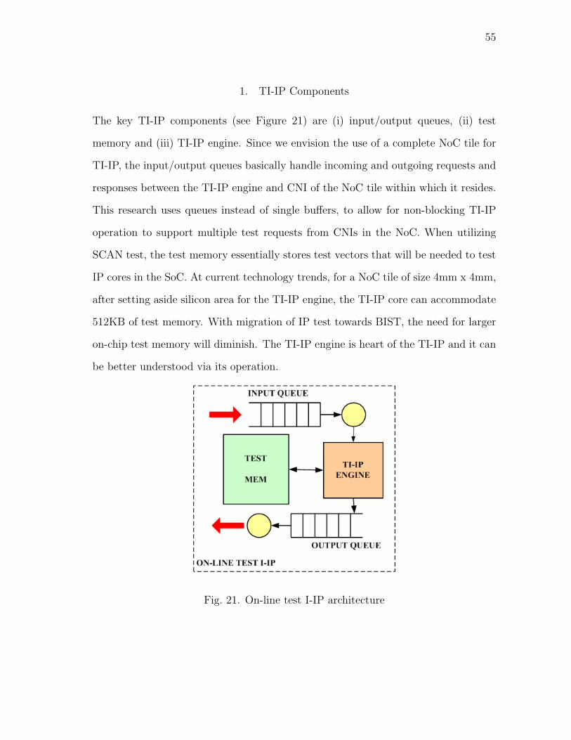
55
1. TI-IP Components
The key TI-IP components (see Figure 21) are (i) input/output queues, (ii) test
memory and (iii) TI-IP engine. Since we envision the use of a complete NoC tile for
TI-IP, the input/output queues basically handle incoming and outgoing requests and
responses between the TI-IP engine and CNI of the NoC tile within which it resides.
This research uses queues instead of single buffers, to allow for non-blocking TI-IP
operation to support multiple test requests from CNIs in the NoC. When utilizing
SCAN test, the test memory essentially stores test vectors that will be needed to test
IP cores in the SoC. At current technology trends, for a NoC tile of size 4mm x 4mm,
after setting aside silicon area for the TI-IP engine, the TI-IP core can accommodate
512KB of test memory. With migration of IP test towards BIST, the need for larger
on-chip test memory will diminish. The TI-IP engine is heart of the TI-IP and it can
be better understood via its operation.
Fig. 21. On-line test I-IP architecture

56
2. TI-IP Operation
The operations to be supported by the TI-IP include (i) servicing test requests, and
(ii) managing concurrent on-line testing. It achieves this by collaborating with the
CNIs in the NoC and other TI-IPs in the design. The CNI (a) initiates test requests,
(b) forwards test data to IP cores from TI-IP, (c) test responses from the IP cores to
the TI-IP and (d) monitors IP core utilization with the help of an IP core monitoring
unit. The function of the IP core monitor is to determine IP core utilization. We do
not provide technical details regarding this, since it will vary depending on the type
of IP cores. For the purpose of our experiments, we treat this as a black box capable
of monitoring utilization of the IP core it is attached to. This collected information
will aid the TI-IP in assessing the feasibility of concurrent test. As stated earlier, for
concurrent on-line testing of SoCs, the CNI is responsible for issuing test requests to
the TI-IP for the IP cores attached to it. Determining the frequency of test is an
interesting and challenging task by itself. For the purpose of this research, we assume
that the CNI requests for test periodically. The frequency of test request depends
on (i) technology, (ii) utilization and (iii) criticality of the core. Future research will
formalize this concept. Test request can also be event-based and is an option being
explored in other research.
The on-line testing of a SoC is performed in a number of stages. A FSM sum-
marizing these is shown in Figure 22, while Figure 23 elaborates on the expected
timeline of execution for a multi-core SoC with on-line testing enabled. The signal
arcs of the FSM are discussed in Section V.A. The rest of this section describes the
activities in the various stages of TI-IP operation.
Test Request (TR): The TR stage involves the CNI issuing a request for test of
the IP cores attached to it. As mentioned earlier, test request frequency depends on

57
a number of factors and is assumed to be periodic for this research.
System Snapshot Determination (SSD): To aid in ascertaining feasibility of
Fig. 22. TI-IP FSM
test in presence of executing applications, the TI-IP obtains a system snapshot (SS),
by issuing a request to all CNIs in the SoC. The CNIs collect utilization informa-
tion from IP monitors and provide it to the TI-IP. A timestamp is associated with
SS information to prevent use of stale information in Test Acceptance. The system
snapshot information is maintained in the System Snapshot Table (SST) in the TI-IP.
The fields of the SST are listed in Table V.
By virtue of using a packet-switched interconnection network to provide com-
munication between on-chip cores, network latency can degrade the freshness of the
system snapshot information collected by the TI-IP. In smaller NoCs, this is not a
major concern. But in larger designs this issue can be resolved by weighting informa-

58
Fig. 23. SoC operation timeline with integrated COLT
Table V. System snapshot table fields
Sender ID Network address of source network tile
Measured Utilization This field stores utilization values returned by CNIs
Timestamp This field is used to indicate freshness of utilization value
Test Request This field indicates CNI requesting test
tion delivered from farther CNIs. The Test Throttling mechanism discussed later in
this dissertation provides sufficient protection against power budget violations.
Test Acceptance (TA): In the TA stage, a routing solution for test vector deliv-
ery from test memory to the target IP core is determined and using SS information,
the feasibility of test is made. Test feasibility is determined using utilization met-
rics. Equation 4.1 aids in deciding whether a requested test can be accepted within

59
intrusion bounds.
∑i∈IPcores
Ui +∑
j∈NoCcomponents
Uj +∑
k∈Core−under−test
Uk +∑
l∈linksonpath
Ul ≤ 1.0 (4.1)
where, the U terms are the utilization indices of the components in the SoC. The
first two terms measure utilization of the IP cores and NoC components. The third
term measures the utilization of the IP cores under test. The final term considers
cost of test vector delivery to the IP core requesting test. These utilization indices
are normalized using (i) the measured IP core utilization, (ii) a multiplier and (iii)
total power budget. The multiplier normalizes measured core utilization with system
power budget and can be determined from the core specifications. By using this uti-
lization index as a prediction of SoC utilization we determine the feasibility of test.
Once accepted, the test is scheduled and queued into the output queue of the TI-IP.
When test requests are rejected, corresponding messages have to be provided to the
requesting CNIs.
Test Delivery (TD): In the TD stage, test vectors are delivered over the NoC via
the route determined in TA stage. The intended target is the CNI attached to the
IP core that requested the test. When SCAN testing multiple cores simultaneously,
to prevent starvation test vector delivery to the multiple cores is interleaved. Test
vector delivery is paced to prevent buffer overflow on the intermediate hops and at
the destination test site.
Test Application (TAP): Test vectors are applied to the IP core in this stage. CNI
receives test vectors from the TI-IP. The test wrapper prepares these for application
to the IP cores. COLT does not advocate a particular type of test for the IP cores.
This will be IP core specific. The TI-IP can support both SCAN and BIST. Due
to large test times, the IP core may not be completely testing in a single attempt.
Partial test may be performed based on the availability of idle periods.

60
Test Response Collection (TRC): Once test vector application completes, test re-
sponse collection and comparison needs to be performed before the TI-IP can respond
with a recovery scheme. The comparison can either be performed at the application
site, i.e. the CNI attached to the IP core being tested, or at the TI-IP. In the for-
mer case, the expected response will have to be sent to the CNI, while in the latter,
the test responses need to be forwarded to the TI-IP. Trade-offs involved in selecting
between TRC implementation includes buffer storage at the CNI, processing delays
at TI-IP due to multiple test response comparisons and test response delivery energy
consumption.
TI-IP Response (TPR): After evaluation of test response completes, the TI-IP
has to respond to detected phenomenon. This response could include system recon-
figuration, IP core shutdown, communication rerouting and application termination.
This response depends on the type of SoC configuration and is a part of the on-line
health management system. Since this research is focused on COLT, SoC recovery is
not discussed here.
CNI Alarm Handler: In this stage, when the CNI detects utilization mis-prediction,
it sends a cni alarm message to the TI-IP. The TI-IP throttles IP core test by modi-
fying the pace of test vector delivery, thereby controlling test power consumption.
TI-IP Configuration: In the TI-IP configuration stage, the TI-IP Configuration
Table is populated with the test related information and is loaded when the SoC is
deployed and initialized. The fields of this configuration table are listed in Table VI.
3. Multi TI-IP Operation
To manage the test power efficiently in larger SoCs a single TI-IP in the design will
not be sufficient. Energy consumed in delivering test vectors from test memory to

61
Table VI. TI-IP configuration table fields
Tile ID This field indicates the network tile ID.
Test Type This field indicates the type of test support by the IP
core, i.e. SCAN or BIST.
Test Volume This field indicates the test volume associated with this
test entry.
Test Memory Pointer This field provides a pointer to the
test vectors in the test memory.
the IP cores is directly proportional to the distance between them and the volume
of the test data. Figure 24 demonstrates how this energy consumption grows with
test volume and hop distance. This provides adequate motivation for the formulation
of a multi-TI-IP technique to test larger SoCs. In such a scenario, multiple TI-IPs
provide for energy efficient testing by reducing the average hop distance for test vector
delivery. But the introduction of additional TI-IPs makes it difficult to ensure power
constrained testing without co-operation between these TI-IPs.
Introducing multiple TI-IPs into a SoC design is not a trivial solution, since they
have to co-operate in test decisions. For this research we configured the TI-IPs to
operate in a token ring manner. In this case, only the TI-IPs with the test manage-
ment tokens are permitted to schedule test of the IP cores. To manage this aspect,
the Test Management Token Handler state was added into the TI-IP controller FSM
in Figure 22. The multi-TI-IP configuration also introduces an additional task of
mapping IP core test responsibility to the individual TI-IPs. For our initial experi-
ments, we have assigned test responsibilities based on proximity. A formal technique
considering test parameters and design constraints is currently being assessed.

62
Fig. 24. Proximity effect on test vector delivery energy consumption
D. Robust Protocol for COLT
Following extensive simulation and functional validation of TI-IP operation, exposed
hazards which prevented correct operation of COLT. This motivated the development
of robust COLT operation. This section addresses the robustness aspect of COLT
communication protocol by specifying the communication protocol, identifying pro-
tocol hazards and describing hazard mitigation techniques.
1. Protocol Specification
Protocol Step 1: Test Request
This step of the protocol involves the TI-IP and CNI of IP core requesting test.
On the occurrence of the test request event, the CNI issues a test request (TReq)
command to the TI-IP. Before issuing a test response, the TI-IP executes the System
Snapshot Collection protocol step and performs the Test Acceptance operation dis-
cussed in the previous section. The Test Acceptance step decision is provided to the

63
CNI of IP requesting test via a test request response (TReqResp) command. Figure 25
illustrates this protocol step.
Fig. 25. Test request protocol step
Protocol Step 2: System Snapshot Collection
This protocol step involves the TI-IP and CNIs of all network tiles in the NoC.
The TI-IP issues a system snapshot request (SSReq) command to all the CNIs. The
CNIs respond with system snapshot response (SSResp) command to all TI-IPs in the
NoC. Figure 26 illustrates this protocol step. This requires the CNIs to be aware of
all TI-IPs in the SoC. As mentioned earlier, this system snapshot response provides
utilization information for the IP core attached to that CNI.
Protocol Step 3: Test Vector Delivery
This protocol step involves the TI-IP and CNIs of IP cores requesting test. When
using SCAN test, TI-IP delivers test vectors to these CNIs in an interleaved manner.
The interleaved delivery is needed prevent test starvation due to large test vector
volume. Figure 27 assumes a scenario where 3 IP cores have successfully requested
concurrent on-line test and are in Test Vector Delivery COLT protocol step.
Protocol Step 4: Test Management Token Transfer
In the multiple TI-IP configuration, to allow for co-operative testing of IP cores,

64
Fig. 26. System snapshot collection protocol step
Fig. 27. Test vector delivery protocol step

65
TI-IPs need a Test Management Token. As discussed in Section 3, the TI-IP with the
Test Management Token is the only TI-IP allowed to schedule COLT. The multiple
TI-IPs are configured in a token ring configuration and they periodically exchange
the Test Management Token. Figure 28 illustrates a 3 TI-IP configuration where the
TI-IPs periodically exchange tokens.
Fig. 28. Test management token transfer protocol step
Protocol Step 5: Test Throttle
Since test acceptance and scheduling is predictive in nature and depends on
history information in the form of IP core utilization, the introduction of new appli-
cations into the system, may render collected information to be invalid. To account
for mis-predicted system utilization information (also referred to as misbehaving ap-
plications), the TI-IP has to be able to throttle concurrent on-line test. The need
for such a mechanism is dominant in scenarios with dynamically changing application
characteristics. Periodic and well-behaved applications would not utilize this protocol
step. The participants in this protocol step are the TI-IPs, CNIs of ”misbehaving”
IP cores and CNIs of IP cores-under-test. When misbehavior is detected, the CNI
issues a CNI alarm (CNIAlarm) command to the TI-IP. The TI-IP then determines
whether any concurrent tests need to be reconfigured. It can control two aspects

66
of concurrent test reconfiguration: (a) alter test vector delivery pace and (b) halt
test application on IP cores-under-test. Figure 29 illustrates the CNI Alarm issuance
and the corresponding test throttle (TThrottle) command delivery to CNIs of IP
cores-under-test.
Fig. 29. Test throttle protocol step
2. Protocol Hazards
The following are hazards presented by the protocol specification to concurrent on-
line testing of the SoC. The impact of each hazard on the communication protocol
steps is also described.
Hazard 1: Starvation due to Application/Test
Since application and test communication flow over a common communication
infrastructure, large volumes of application (test) data can starve test (application)
data. Impact of hazard on the communication protocol steps are discussed below:
1. Test Request: Starvation due to application can prevent test requests from
flowing to the TI-IPs, prevent on-line test.
2. System Snapshot Collection: Starvation due to application can prevent the CNI
from responding to system snapshot request commands.

67
3. Test Vector Delivery: Starvation due to applications can prevent test vector
delivery to the test wrappers. High test vector volume can also lead to starvation
due to test at the TI-IP.
4. Test Management Token Transfer: Starvation due to high test vector volume
can prevent test management token transfer.
5. Test Throttle: Starvation due to application can prevent the CNI alarm from
being delivered to the TI-IP. Starvation due to high test vector volume can
also prevent Test Throttle command from being delivered from TI-IP to CNI
of cores-under-test.
Hazard 2: Test Input Queue buffer overflow
The Test Input Queue buffer overflow hazard can prevent the TI-IP from receiv-
ing commands critical to concurrent on-line testing. This hazard has an impact on
all protocol steps of COLT.
Hazard 3: TI-IP Failure
The TI-IP Failure hazard can prevent the concurrent on-line testing of the SoC.
In the single TI-IP configuration, the major impact of the failure is loss of concurrent
on-line test capability. In a multi TI-IP configuration, the testability of the SoC is
reduced, since test of IP cores assigned to the failed TI-IP may not be transferable to
other TI-IPs in multi TI-IP configuration. Impact on the following communication
protocol steps:
1. Test Request: TI-IP failure can prevent test request command handling.
2. System Snapshot Collection: TI-IP failure prevents snapshot collection.
3. Test Vector Delivery: TI-IP failure prevents on the delivery of test vectors to
IP cores being tested by the failed TI-IP.

68
4. Test Management Token Transfer: This hazard can result in the loss of the Test
Management Token in the multi TI-IP configuration.
5. Test Throttle: This hazard can lead to constraint violation due to concurrent
on-line test.
Hazard 4: Test Wrapper buffer overflow
The test wrapper buffer overflow hazard will lead to loss of test vector data for
test of IP cores. This hazard only has impact on the Test Vector Delivery protocol
step.
Hazard 5: CNI Failure
This hazard prevents correct operation of the CNI. CNI failure can lead to the
isolation of the network tile from the rest of the NoC.
3. Hazard Mitigation
This subsection discusses the approaches taken to circumvent potential hazards iden-
tified in the previous sub-section.
Hazard 1 Mitigation: Starvation due to application/test
1. Test Request: For this protocol step, to mitigate hazard 1, test would need
to be assigned priority over application. Temporarily swapping priorities can
resolve this hazard.
2. System Snapshot Collection: Hazard mitigation for this protocol step involves
the usage of the timeout value. Once timeout occurs, the CNI being starved by
application is assumed to be busy and in high utilization mode.
3. Test Vector Delivery: To mitigate this hazard, priorities of application and test
would need to be swapped.

69
4. Test Management Token Transfer: Interleaving outgoing communications from
Test Output Queue of TI-IP addresses all starvation concerns.
5. Test Throttle: To mitigate this hazard, priorities of application and test would
need to be swapped.
Hazard 2 Mitigation: Test Input Queue buffer overflow
The test input queue buffer overflow hazard is mitigated by requesting a retrans-
mission from the source CNI. This technique would require additional buffering at
the source CNI.
Hazard 3 Mitigation: TI-IP failure
Hazard 3 mitigation techniques are only applicable in multi TI-IP configuration.
1. Test Request: CNIs in the NoC need to communicate with all TI-IPs in the
SoC. When a TI-IP failure event is detected, all CNIs need to be informed.
When using SCAN test, IP core test responsibilities cannot be handed over to
alternative TI-IPs since test vector data is only assigned to TI-IP responsible
for the test. Responsibility hand off is easier for BIST of cores.
2. System Snapshot Collection: Mitigating the hazard during the system snapshot
collection protocol step is not possible. It requires hand off of test responsibili-
ties, if possible.
3. Test Vector Delivery: TI-IP failure during the Test Vector Delivery protocol
step will prevent successful test of the IP cores assigned to it.
4. Test Management Token Transfer: Mitigating this hazard is considerably more
difficult when more than 2 TI-IPs are deployed in the multi TI-IP configuration.
A complex election protocol amongst the TI-IPs is required to recover the lost
token.

70
5. Test Throttle: TI-IP failure can prevent test throttling of tests initiated by
the failed TI-IP. Mitigation of this hazard can be achieved by exchanging IP
core test status between TI-IPs in the SoC. This can be coupled with Test
Management Token Transfer protocol step.
Hazard 4 Mitigation: Test wrapper buffer overflow
Test wrapper buffer overflow is prevented by scheduling test vector delivery to
test wrapper of IP core-under-test. Since test vector delivery at the TI-IP source is
interleaved, test vector block sizes sent out in a single iteration have an upper bound
stipulated by the test wrapper buffer capacity.
Hazard 5 Mitigation: CNI failure
CNI failure is a hazard that cannot be mitigated. However, once detected, the
event should be registered with TI-IPs to prevent wasted effort due to unnecessary
communication between TI-IP and failed CNIs.
E. Experimental Setup and Results
1. NoCSim Modification
A SystemC functional model of the proposed TI-IP has been embedded into a network
tile in NoCSim and is used to manage test of IP cores embedded in the design. It
does so through the embedded CNI model and generic test wrapper around the IP
core modules. Minor modifications to the packet headers were also required to allow
for special handling of flits in the CNIs.
2. ITC’02 SoC Test Benchmark
In the absence of an actual SoC design with corresponding applications and test
configurations, the ITC’02 SoC Test Benchmarks [57] and Embedded Systems Syn-

71
thesis Benchmark Suite (E3S) [58] are used to provide the test configuration and
application configuration information, respectively. The ITC’02 benchmarks provide
sufficient test data for modular designs, to allow researchers to solves problems in the
domain of TAM design, test scheduling and wrapper design.
The benchmark provides typical SoC test parameters - test volume and test exe-
cution time. Test power consumption for most of these is unavailable. Since research
has shown that power consumption in test mode to be about 1.5x normal mode power
consumption [48], we utilize this knowledge to estimate test power consumption for
the selected IP cores in our test configurations.
3. Embedded Systems Synthesis Benchmark Suite
The E3S is used to provide application related information for our test configura-
tions. Relevant E3S information for this research included power, area and execution
times for 47 tasks from 5 application domains on 17 commercial processors. Task
graphs from the 5 application domains were embedded into two SoC configurations
in NoCSim as illustrated in Figure 30.
4. Test Configurations
Assuming a chip size of 22mm x 22mm [4], consisting of network tiles sized at 4mm
x 4mm, the IBM 405GP processor was selected from E3S processor list. Using the
relevant specifications of the IBM 405GP (idle power, peak power and clock rate), the
network tiles in NoCSim were configured accordingly to provide the compute support
to applications.
Two baseline SoC configurations were also developed using the tasks graphs in
E3S. soc config1 was assigned 11 task graphs spanning 4 application domains - office
automation, consumer, networking and auto industry. These were mapped onto a 4 x

72
Fig. 30. Experimental SoC configurations
4 2D torus utilizing 13 network tiles (i.e. execute on 13 IBM 405GPs). The mapping
of the tasks has an impact on the performance of the design [31], but for the purpose
of this research, we mapped the task graphs by hand. The test parameters of the
cores were assigned based on the g1023.soc ITC’02 benchmark.
The second SoC configuration (soc config2) also utilized the IBM 405GP and
had 9 task graphs from the telecom application domain mapped over 11 network
tiles. Test parameters were assigned based on the d695.soc ITC’02 SoC benchmark.
Figure 31 below illustrates the mapping of the test core specifications onto the cor-
responding network tiles. The digits in the tile correspond to the core id in the
benchmark specification. Using these two baseline configurations, four additional
configurations were prepared, differing in the number of TI-IPs assigned and their
locations in the design. Figure 30 illustrates these additional configurations. To il-

73
lustrate how the TI-IP would operate in the absence of executing applications, four
additional configurations with just TI-IPs were also prepared. We report power pro-
files and finish time variations on these ten configurations in the following sub-section.
It must be noted here, that the simulations in NoCSim do not actually run the ap-
plications or the test benchmarks, but instead characterizes execution profiles of the
system which is reflected in the power profiles.
Fig. 31. ITC’02 SoC test benchmark mapping to experimental configurations
5. TI-IP Validation
a. SoC Configuration 1
Figure 32 illustrates the power profile comparison between the 3 variations (applica-
tions only, test only and applications + test) of this configuration. In the simulation
interval specified and for the configured input test parameters (from ITC’02 bench-
marks), only a single IP core was tested. The power variation in this case is not
much. When the parameters were altered to allow 2 additional IP cores to be tested,
the power profile in Figure 33 was observed. This demonstrated the sensitivity of
the concurrent testing to the test parameters. For comparison purposes, the power

74
0 0.2 0.4 0.6 0.8 1 1.2 1.4 1.6 1.8 2
x 106
0
0.05
0.1
0.15
0.2
0.25
0.3
0.35
0.4
Time (cycles)
Pow
er (
Wat
ts)
SoC Configuration 1 (TI−IP Configuration 1): Power Profile
Application w/o TI−IPTI−IP onlyApplication w/ TI−IP
Fig. 32. SoC configuration 1 power profile, 1 IP core tested
0 0.2 0.4 0.6 0.8 1 1.2 1.4 1.6 1.8 2
x 106
0
0.05
0.1
0.15
0.2
0.25
0.3
0.35
0.4
0.45
Time (cycles)
Pow
er (
Wat
ts)
SoC Configuration 1 (TI−IP Configuration 1): Power Profile
Application w/o TI−IPTI−IP onlyApplication w/ TI−IP
Fig. 33. SoC configuration 1 power profile, 3 IP cores tested

75
profile for just the IP cores testing has also been plotted in the same.
When multiple TI-IPs were deployed into the design (soc config1 tiip2), similar
power trends were observed (see Figure 34), with one exception: fewer cores were
tested in this configuration, since the TI-IP responsible for testing those cores did
not have the test management token, highlighting the consequence of the IP core test
responsibility mapping to individual TI-IPs.
When the average task execution times of the task graphs in soc config1 were
analyzed, there were no variations observed. This is attributed to the fact that the
IP core that was tested, was not executing any tasks at that time, which highlights
the test scheduling aspect and the need for an accurate on-line monitoring scheme
to detect when to test an IP core. Figure 35 compares the power profiles of the two
TI-IP configurations.
0 0.2 0.4 0.6 0.8 1 1.2 1.4 1.6 1.8 2
x 106
0
0.05
0.1
0.15
0.2
0.25
0.3
0.35
0.4
Time (cycles)
Pow
er (
Wat
ts)
SoC Configuration 1 (TI−IP Configuration 2): Power Profile
Application w/o TI−IPTI−IP onlyApplication w/ TI−IP
Fig. 34. SoC configuration 1 power profile, multi TI-IP setup

76
0 0.2 0.4 0.6 0.8 1 1.2 1.4 1.6 1.8 2
x 106
0
0.05
0.1
0.15
0.2
0.25
0.3
0.35
0.4
Time (cycles)
Pow
er (
Wat
ts)
SoC Configuration 1 (TI−IP Configuration 1 vs TI−IP Configuration 2): Power Profile
TI−IP1 onlyTI−IP2 onlyApplication w/ TI−IP1Application w/ TI−IP2
Fig. 35. SoC configuration 1 comparing single TI-IP with multi TI-IP setup power
profiles
b. SoC Configuration 2
In this test configuration, the observed power profile was similar in observed trends to
that of SoC configuration 1 (see Figure 36 and Figure 37). Since the test configuration
for this was based on d695.soc, the different test specifications demonstrated different
operational characteristics (in terms of test power profile), especially in the TI-IP
only scenarios. In TI-IP configuration 1 (single TI-IP), 9 IP cores were tested, while
in TI-IP configuration 2 (two TI-IPs), 4 IP cores were tested. As observed earlier, this
is due to the IP core test responsibility mapping to the individual TI-IPs discussed
earlier.
Figure 38 illustrates the power profile comparison between the single TI-IP and
multi TI-IP configurations for SoC configuration 2.
For this test configuration, a finish time variation of 1% was observed for a task

77
graph 4 in the system. But this variation did not lead to any deadline misses.
0 0.2 0.4 0.6 0.8 1 1.2 1.4 1.6 1.8 2
x 106
0
0.05
0.1
0.15
0.2
0.25
0.3
0.35
0.4
Time (cycles)
Pow
er (
Wat
ts)
SoC Configuration 2 (TI−IP Configuration 1): Power Profile
Application w/o TI−IPTI−IP onlyApplication w/ TI−IP
Fig. 36. SoC configuration 2 power profile, single TI-IP setup
6. Robust Protocol Validation
Figure 39 demonstrates the energy profile for the system snapshot collection and
beginning of test application on an IP core in the NoC. The normal on-line test mode
curve is compared to the case of test starvation due to communication intensive
application. The timeout based mitigation technique delays start of test application.
In the absence of this technique, no test application would take place.
A test case to demonstrate test throttling due to misbehaving application is
demonstrated in Figure 40. Since only SCAN test data was available, the TI-IP
reduced the pace of test vector delivery to reduce test energy consumption.

78
0 0.2 0.4 0.6 0.8 1 1.2 1.4 1.6 1.8 2
x 106
0
0.05
0.1
0.15
0.2
0.25
0.3
0.35
0.4
Time (cycles)
Pow
er (
Wat
ts)
SoC Configuration 2 (TI−IP Configuration 2): Power Profile
Application w/o TI−IPTI−IP onlyApplication w/ TI−IP
Fig. 37. SoC configuration 2 multi TI-IP setup power profile
0 0.2 0.4 0.6 0.8 1 1.2 1.4 1.6 1.8 2
x 106
0
0.05
0.1
0.15
0.2
0.25
0.3
0.35
0.4
Time (cycles)
Pow
er (
Wat
ts)
SoC Configuration 2 (TI−IP Configuration 1 vs TI−IP Configuration 2): Power Profile
TI−IP1 onlyApplication w/ TI−IP1TI−IP2 onlyApplication w/ TI−IP2
Fig. 38. SoC configuration 2 single TI-IP vs multi TI-IP power profile

79
Fig. 39. Energy profile demonstrating starvation hazard mitigation
Fig. 40. Energy profile demonstrating TI-IP test throttling effect on misbehaving ap-
plication

80
7. Synthesis Results
An HDL implementation of the TI-IP was synthesized with Synopsys Design Com-
piler [35] using the Virginia Tech VLSI for Telecommunications TSMC-0.25um, 2.5V
standard cell library [36, 37], the gate count for the TI-IP was estimated at 83K and
power consumption estimated was 520mW (leakage: 32uW).

81
CHAPTER V
SUMMARY
A. Conclusions
This dissertation presents an architecture for the CNI that provides services beyond
the basic packetization and de-packetization. A 5-stage pipelined implementation
of the CNI was analyzed and included into NoCSim for functional verification. We
also propose a scheme to manage end-to-end latency jitter by using class-based VC
allocation. In the absence of such a scheme, for a particular configuration of the NoC,
latency jitter of 400% was observed. Using such a scheme provides for predictable
end-to-end latency. The modified VC allocation scheme was included into NoCSim to
evaluate the jitter bounding capability in the end-to-end latency. Performance over
varying hop distances was evaluated. A processor-memory setup was configured and
at two cache miss rates, the throughput of the system was evaluated.
With increasing contribution of on-chip communication power to total system
power consumption, a dynamic peak power management scheme is essential for re-
liability and cooling considerations. This research proposed SAPP, a scalable and
adaptable peak power management technique. Using non-deterministic, independent
and dynamic peak power budget re-allocation in NoCs, it provides for a scalable and
adaptable technique for large designs where communication characteristics are un-
available. The autonomous nature of SAPP makes it applicable to any NoC design.
Other schemes in research literature suffer from scalability and adaptability concerns
that are addressed by SAPP. An average flit latency improvement of 47% was observed
for non-uniform load injection distribution. Effective throughputs showed an average
improvement of 36%. Higher utilization of allocated peak power budget provides for

82
the observed performance improvement.
With reducing lifetime reliability in complex SoC designs and challenges in es-
timating MTTF, deployment of a concurrent on-line SoC test framework is the next
step to address rising test costs. This research proposes the introduction of a test
infrastructure IP into a SoC design to provide on-line test support in presence of
executing applications. Previous works consider SoC test in the absence of applica-
tion, but prohibitive test times make turning off of the system infeasible. To address
scalability aspects, the designed TI-IPs are capable of operating in a multi-TI-IP con-
figuration, in which they co-operatively handle concurrent on-line test responsibilities.
A NoC-based SoC design is considered as it provides for a superior communication
infrastructure. Basic operation of the TI-IP is outlined and a functional model is
included into NoCSim. Using application benchmarks (E3S) and SoC test bench-
marks (ITC’02 SoC Test bench), two baseline SoC configurations and their eight
TI-IP variations were built and simulated on. Experiments demonstrated the correct
operation of the TI-IP. For this research we only consider SCAN testing of IP cores
due to the lack of BIST test data. BIST support has been included in the current
version of the TI-IP, but has not been tested with actual BIST test benches. Com-
munication protocol specifications are also presented in this dissertation. Potential
hazards to concurrent on-line testing have been identified and techniques to mitigate
them have been proposed. Experimental results demonstrate robust operation of the
communication protocol.
B. Future Work
For autonomous on-line health management for SoCs, a concurrent on-line test, diag-
nosis and recovery mechanism is essential. This research addresses the complex issue

83
of concurrent on-line test. Diagnosis and recovery functionality has to be integrated
into the TI-IP. Investigation into an efficient global ordering mechanism for NoC is
also required.

84
REFERENCES
[1] G. E. Moore, “Cramming more components onto integrated circuits,” Electron-
ics Magazine, vol. 38, pp. 114–117, 1965.
[2] “International Technology Roadmap for Semiconductors,” http://www.itrs.net/,
cited July 11, 2006.
[3] P. Guerrier and A. Greiner, “A generic architecture for on-chip packet-switched
interconnections,” in Proc. IEEE Design, Automation and Test in Europe Con-
ference and Exhibition (DATE), 2000, pp. 250–256.
[4] B. Towles and W. J. Dally, “Route packets, not wires: on-chip interconnection
networks,” in Proc. ACM/IEEE Design Automation Conference (DAC), 2001,
pp. 684–689.
[5] L. Benini and G. De Micheli, “Networks on chips: a new SoC paradigm,” IEEE
Computer, vol. 35, pp. 70–78, 2002.
[6] R. K. Gupta and G. D. Micheli, “Hardware Software cosynthesis for digital
systems,” IEEE Design and Test, pp. 29–41, 1993.
[7] J. Hu and R. Marculescu, “Energy-aware mapping for tile-based NoC architec-
tures under performance constraints,” in Proc. Asia and South Pacific Design
Automation Conference (ASP-DAC), 2003, pp. 233–239.
[8] K. Srinivasan and K. S. Chatha, “A technique for low energy mapping and
routing in network-on-chip architectures,” in Proc. IEEE/ACM Intl. Symp. on
Low Power Electronic Design (ISLPED), 2005, pp. 387–392.

85
[9] Praveen S. Bhojwani, “Mapping multimode system communication to a network-
on-a-chip (NoC),” M.S. thesis, Texas A&M University, College Station, Texas,
December 2003.
[10] T. Ahonen, D. S. Tortosa, and J. Nurmi, “Topology optimization for application-
specific networks-on-chip,” in Proc. 6th Intl. Workshop on System Level Inter-
connect Prediction, 2004, pp. 53–60.
[11] Y. Hu, H. Chen, Y. Zhu, A. A. Chien, and Chung-Kuan Cheng, “Physical
synthesis of energy-efficient networks-on-chip through topology exploration and
wire style optimization,” in Proc. Intl. Conf. on Computer Design (ICCD), 2005,
pp. 111–118.
[12] K. Srinivasan, K. S. Chatha, and G. Konjevod, “An automated technique for
topology and route generation of application specific on-chip interconnection net-
works,” in Proc. IEEE/ACM Intl. Conf. on Computer-aided Design (ICCAD),
2005, pp. 231–237.
[13] K. Srinivasan and K. S. Chatha, “ISIS: A genetic algorithm based technique for
custom on-chip interconnection network synthesis,” in Proc. 18th Intl. Conf. on
VLSI Design (IVLSI), 2005, pp. 623–628.
[14] K. Srinivasan and K. S. Chatha, “SAGA: Synthesis technique for guaranteed
throughput NoC architectures,” in Proc. Asia South-Pacific Design Automation
Conference (ASPDAC), 2005, pp. 489–494.
[15] K. Srinivasan, K. S. Chatha, and G. Konjevod, “Application specific network-
on-chip design with guaranteed quality approximation algorithms,” in Proc. Asia
South-Pacific Design Automation Conference (ASPDAC), 2006, pp. 184–190.

86
[16] Y. Jin and E. J. Kim K. H. Yum, “Peak power control for a QoS capable on-chip
network,” in Proc. Intl. Conf. on Parallel Processing (ICPP), 2005, pp. 585–592.
[17] L. Shang, L-S. Peh, and N. K. Jha, “PowerHerd: dynamically satisfying peak
power constraints in interconnection networks,” in Proc. Intl. Sym. Supercom-
puting (ICS), 2003, pp. 98–103.
[18] T. Dumitras, S. Kerner, and R. Marculescu, “Towards on-chip fault-tolerant
communication,” in Proc. Asia and South Pacific Design Automation Conference
(ASP-DAC), 2003, pp. 225–232.
[19] P. S. Bhojwani, R. Singhal, G. Choi, and R. N. Mahapatra, “Forward error
correction for on-chip interconnection networks,” in Proc. Workshop on Unique
Chips and Systems (UCAS), March 2006, pp. 41–48.
[20] F. Worm, P. Ienne, P. Thiran, and G. De Micheli, “An adaptive low-power
transmission scheme for on-chip networks,” in Proc. 15th Intl. Symp. on System
Synthesis (ISSS), 2002, pp. 92–100.
[21] P. S. Bhojwani and R. N. Mahapatra, “An infrastructure IP for on-line testing of
network-on-chip based SoCs,” in Proc. IEEE Intl. Symp. on Quality Electronic
Devices (ISQED), March 2007, pp. 867–872.
[22] P. S. Bhojwani and R. N. Mahapatra, “A robust protocol for concurrent on-
line test (COLT) of NoC-based systems-on-a-chip,” in Proc. ACM/IEEE Design
Automation Conference (DAC), June 2007, pp. 670–675.
[23] “OCP Specification Release 2.0,” Technical Report, http://www.ocpip.org, ac-
cessed January 16, 2004.
87
[24] “VSI Alliance - Virtual Component Interface Standard (OCB 2.2.0),” Technical
Report, http://www.vsi.org, accessed March 3, 2003.
[25] “AMBA Specification,” Technical Report, http://www.arm.com/products/-
solutions/AMBAHomePage.html, accessed January 16, 2004.
[26] P. S. Bhojwani and R. N. Mahapatra, “Interfacing cores with on-chip packet-
switched networks,” in Proc. IEEE 16th Intl. Conf. on VLSI Design, January
2003, pp. 382–387.
[27] “Xtensa Configurable Processor,” Technical Report, http://www.tensilica.com,
accessed March 3, 2003.
[28] A. Radulescu and K. Goossens, “Communication Services for Networks on
Chip,” in Domain-Specific Processors: Systems, Architectures, Modeling, and
Simulation (SAMOS), 2002, pp. 275–299.
[29] D. Bertozzi, L. Benini, and G. De Micheli, “Low power error resilient encoding
for on-chip data buses,” in Proc. IEEE Design, Automation and Test in Europe
(DATE), 2002, pp. 102–109.
[30] R. Gallager, “Low-density parity-check codes,” IRE Transaction Information
Theory, vol. IT-8, pp. 21–28, 1962.
[31] P. S. Bhojwani, E. J. Kim, R. N. Mahapatra, and T. Chen, “A heuristic for peak
power constrained design of network-on-chip (NoC) based multimode systems,”
in Proc. IEEE 18th Intl. Conf. on VLSI Design, January 2005, pp. 124–129.
[32] C. Ciordas, T. Basten, A. Radulescu, K. Goossens, and J. Meerbergen, “An
event-based network-on-chip monitoring service,” in Proc. IEEE 9th Intl. High-
Level Design Validation and Test Workshop, 2004, pp. 149–154.

88
[33] M. Nahvi and A. Ivanov, “Indirect test architecture for SoC testing,” IEEE
Trans. on Computer-Aided Design of Integrated Circuits and Systems, vol. 23,
pp. 1128–1142, 2004.
[34] W-D. Weber, “A quality-of-service mechanism for interconnection networks in
systems-on-chips,” in Proc. IEEE Design, Automation and Test in Europe Con-
ference and Exhibition (DATE), 2005, pp. 1232–1237.
[35] “Synopsys Design Compiler,” www.synopsys.com/products/logic/design com-
piler.html, cited July 11, 2007.
[36] J. B. Sulistyo, J. Perry, and D. S. Ha, “Developing Standard Cells for TSMC
0.25um Technology under MOSIS DEEP Rules,” Technical Report VISC-2003-
01, Department of Electrical and Computer Engineering, Virginia Tech, Blacks-
burg, Virginia, November 2003.
[37] J. B. Sulistyo and D. S. Ha, “A New Characterization Method for Delay and
Power Dissipation of Standard Library Cells,” VLSI Design, vol. 15, pp. 667–678,
2002.
[38] L-T. Yeh and R. C. Chu, Thermal Management of Microelectronic Equipment:
Heat Transfer Theory, Analysis Methods, and Design Practices, ASME Press,
New York, New York, 2002.
[39] V. Raghunathan, M. B. Srivastava, and R. K. Gupta, “A survey of techniques
for energy efficient on-chip communication,” in Proc. ACM/IEEE Design Au-
tomation Conference (DAC), June 2003, pp. 900–905.
[40] S. S. Mukherjee, P. Bannon, S. Lang, A. Spink, and D. Webb, “The Alpha 21364
Network Architecture,” IEEE Micro, vol. 22, pp. 26–35, 2002.

89
[41] H. Wang, L.-S. Peh, and S. Malik, “Power-driven design of router microarchi-
tectures in on-chip networks,” in Proc. 36th Annual IEEE/ACM Intl. Symp. on
Microarchitecture, 2003, pp. 105–116.
[42] J. Hu and R. Marculescu, “Exploiting the routing flexibility for en-
ergy/performance aware mapping of regular NoC architectures,” in Proc. IEEE
Design, Automation and Test in Europe (DATE), 2003, pp. 10688–10693.
[43] T. T. Ye, G. De Micheli, and L. Benini, “Analysis of power consumption on
switch fabrics in network routers,” in Proc. ACM/IEEE Design Automation
Conference (DAC), 2002, pp. 524–529.
[44] L. Shang, L-S. Peh, and N. K. Jha, “Dynamic voltage scaling with links for
power optimization of interconnection networks,” in Proc. Intl. Symp. on High-
Performance Computer Architecture (HPCA), 2003, pp. 91–102.
[45] E. J. Kim, K. H. Yum, G. M. Link, N. Vijaykrishnan, M. Kandemir, M. J. Irwin,
M. Yousif, and C. R. Das, “Energy optimization techniques in cluster intercon-
nects,” in Proc. Intl. Symp. on Low Power Electronics and Design (ISLPED),
2003, pp. 459–464.
[46] J. Srinivasan, S. V. Adve, P. Bose, and J. A. Rivers, “Exploiting structural
duplication for lifetime reliability enhancement,” in Proc. 32nd Intl. Symp. on
Computer Architecture (ISCA), 2005, pp. 520–531.
[47] Y. Zorian, “Guest editor’s introduction: what is infrastructure IP?,” IEEE
Design & Test of Computers, vol. 19, pp. 3–5, 2002.
[48] Y. Zorian, “A distributed BIST control scheme for complex VLSI devices,” in
Proc. 11th Annual IEEE VLSI Test Symposium, 1993, pp. 4–9.

90
[49] S. Kumar, A. Jantsch, J. P. Soininen, M. Forsell, M. Millberg, J. Oberg, K. Tien-
syrja, and A. Hemani, “A network on chip architecture and design methodol-
ogy,” in Proc. IEEE Computer Society Annual Symposium on VLSI, 2002, pp.
105–112.
[50] E. Cota, L. Carro, F. Wagner, and M. Lubaszewski, “Power-aware noc reuse on
the testing of core-based systems,” in Proc. Intl. Test Conference (ITC), 2003,
pp. 612–621.
[51] M. Nolen and R. N. Mahapatra, “A TDM test scheduling method for network-
on-chip systems,” in Proc. IEEE 6th Intl. Workshop on Microprocessor Test and
Verification (MTV), 2005, pp. 90–95.
[52] L. Chunsheng, E. Cota, H. Sharif, and D. K. Pradhan, “Test scheduling for
network-on-chip with BIST and precedence constraints,” in Proc. Intl. Test
Conference (ITC), 2004, pp. 1369–1378.
[53] L. Chunsheng, S. Jiangfan, E. Cota, and V. Iyengar, “Power-aware test schedul-
ing in network-on-chip using variable-rate on-chip clocking,” in Proc. IEEE 23rd
VLSI Test Symposium (VTS), 2005, pp. 349–354.
[54] A. Manzone, P. Bernardi, M. Grosso, M. Rebaudengo, E. Sanchez, and M. S.
Reorda, “Integrating BIST techniques for on-line SoC testing,” in Proc. IEEE
11th Intl. On-Line Testing Symposium (IOLTS), 2005, pp. 235–240.
[55] P. Bernardi, M. Rebaudengo, and M. S. Reorda, “Exploiting an I-IP for in-field
SoC test,” in Proc. IEEE 19th Intl. Symp. on Defect and Fault Tolerance in
VLSI Systems, 2004, pp. 404–412.

91
[56] “Online CPU Diagnostics Monitor Version 2.0 Users Guide, Sun Microsys-
tems,” http://www.sun.com/products-n-solutions/hardware/docs/pdf/819-320-
8-10.pdf, cited July 11, 2007.
[57] E. J. Marinissen, V. Iyengar, and K. Chakrabarty, “A set of benchmarks for
modular testing of socs,” in Proc. Intl. Test Conference (ITC), 2002, pp. 519–
528.
[58] “Embedded System Synthesis Suite Benchmark (E3S),”
www.ece.northwestern.edu/ dickrp/e3s, cited July 11, 2007.
[59] D. Liu and C. Svensson, “Power consumption estimation in CMOS VLSI chips,”
IEEE Journal of Solid-State Circuits, vol. 29, pp. 663–670, June 1994.
[60] N. R. Shanbhag, “Reliable and efficient system-on-chip design,” IEEE Com-
puter, vol. 3, pp. 42–50, March 2004.
[61] R. L. Pickholtz, Digital Systems Testing and Testable Design, Computer Science
Press, New York, New York, 1990.
[62] C. Metra and B. Ricco, “Optimization of error detecting codes for the detection
of crosstalk originated errors,” in Proc. IEEE Design, Automation and Test in
Europe (DATE), 2003, pp. 350–355.
[63] S. Lin and D. J. Costello, Error Control Coding: Fundamentals and Applica-
tions, Prentice-Hall, Englewood Cliffs, New Jersey, 1983.
[64] A. Leon-Garcia and I. Widjaja, Communication Networks, McGraw Hill, New
York, New York, 2000.

92
[65] C. Berrou, A. Glavieux, and P. Thitimajshima, “Near Shannon limit error cor-
recting codes and decoding,” in Proc. IEEE Intl. Conf. on Communications,
2003, pp. 225–232.
[66] M. M. Mansour and N. R. Shanbhag, “Low-power VLSI decoder architecture
for LDPC codes,” in Proc. IEEE Intl. Symp. Low Power Electronics and Design
(ISLPED), 2002, pp. 284–289.
[67] D. J. C. Mackay, “Good error-correcting codes based on very sparse matrices,”
IEEE Trans. on Info. Theory, pp. 399–431, 1999.
[68] R. Ho, K. Mai, and M. Horowitz, “Efficient on-chip global interconnects,” in
Symposium on VLSI Circuits, 2003, pp. 271–274.
[69] “Open SystemC Initiative,” www.systemc.org, cited July 11, 2007.

93
APPENDIX A
FORWARD ERROR CORRECTION IN NOCS
A. Introduction
The emergence of NoCs as the communication infrastructure alternative to bus-based
communication in SoCs has presented the SoC design community with numerous
challenges. Designing energy efficient, high performance, reliable systems requires
the formulation of strategies to rectify operational glitches.
The design of low power systems has highlighted the contribution of interconnect
power, upto 50% of total system power [59]. To reduce the interconnect energy con-
sumption, voltage scaling schemes are being used, which in turn reduce the circuit’s
noise margin. The decrease in noise margin makes the interconnect less immune to
errors during transmission. Furthermore internal noises such as power supply noise,
crosstalk noise, and inter signal interference and external noises like thermal noise,
electromagnetic noise, slot noise and alpha-particle induced noise. Thus combining
low-power strategies with data reliability in SoC has become a daunting task for the
designers.
As identified in [60], noise mitigation and tolerance are the two alternatives to
addressing the reliability concerns. But due to the energy inefficiency of the former,
noise tolerance is the preferred approach. In order to deal with interconnect errors in
an energy efficient way, suitable encoding and decoding schemes need to be employed
[39]. Reliability concerns can be addressed using either error detecting codes (EDC)
or error correcting codes (ECC). VLSI self-checking circuits use error detection codes
such as parity, two-rail and other unidirectional EDCs (m-out-of-n and Berger codes)

94
[61]. Since crosstalk is bidirectional [62], these codes would not be sufficient. The
authors in [29] make a case for the use of Hamming code [63] on on-chip data buses,
highlighting its capability to handle single, double errors, its low complexity and
flexibility as a purely detecting code or a purely correcting code. For on-chip networks,
authors in [20] suggest using Hamming code for error detection and in [18] cyclic
redundancy check (CRC) [64] is used to detect errors over every hop. Retransmissions
are then used to correct the detected errors. When it comes to using ECCs in a design,
[29] compares the energy efficiency of forward error correction (FEC) versus error
detection and retransmission for on-chip data buses. The reported results indicate
that FEC is energy inefficient in described applications. However, the overhead for
FEC is expected to subside in emerging NoCs that span large devices using increasing
number of hops and complex buffering/ signaling structures. Use of FEC may be cost
inefficient when the size of the network is small and the cost of the FEC codecs is
high. But as the network size increases and error rates increase, error detection and
retransmission schemes become unacceptable with respect to energy use and latency.
Turbo codes [65] are perhaps the most popular code for FEC in communica-
tion systems and its coding gain approaches very close to Shannon limit. Numerous
researches have revealed the high implementation complexity and the high latency
associated with the turbo decoders. For the low latency and hardware-overhead re-
quirement of the SoC designs, use of Turbo code based FECs is prohibitive. Hamming
codes, on the other hand, can be decoded using simple hardware structures. These,
however, have very poor bit error rate (BER) performance when compared to a simi-
lar rate turbo code. Rivaling the performance of turbo codes, [30] proposed a class of
linear block codes referred to as Low Density Parity Check (LDPC) codes. This code
is suitable for low-latency, high gain, and low power design because of its streamlined
forward-only data flow structure. A number of LDPC decoder architectures have

95
been previously presented. Blanksby presents a 690mW LDPC decoder in [59]. A
low-power decoder architecture was also presented in [66]. The objectives of these
designs are throughput and very high coding gain. The application targets for these
decoders include optical channel, magnetic-media storage, and wireless communica-
tion devices among other error-prone devices. And as consequence, the complexity of
decoder designs presented in the aforementioned papers is very high and infeasible at
the SoC level.
The LDPC code decoder design can be tailored to suite the performance and
overhead requirements imposed by NoC designs. A novel LDPC decoder design that
minimizes the hardware requirement by utilizing only the minimum precision neces-
sary to achieve objective error rate is presented in this dissertation.
Ideally, a transparent forward error correction scheme is desired for SoC ap-
plication. Error correction schemes must be (1) complete, i.e. it does not require
interruption to or from the network controller, (2) compact and power thrifty enough
to be implemented as an integral component of on-chip network interface and (3)
yield high coding gain and cover a wide-range of error models specific to the SoC
design.
B. Related Work
1. FEC Basics
LDPC codes are linear block codes and have a sparse parity check matrix H. A special
class of LDPC codes have H that has the following properties:
• The number of 1s in each column is j
• The number of 1s in each row is k > j

96
Like the other linear block codes, encoding is simple and involves matrix oper-
ations such as addition and multiplication that can be implemented using a highly
regular hardware structure consisting of simple gates. Decoding of LDPC codes is
iterative and uses the Log maximum-likelihood apriori (LOG MAP) algorithm [67].
There are two decoding methods for LDPC decoder: soft decision and hard decision
decoding. In hard decision decoding, the received code word is sampled as 0s or 1s
and then parity check equation is implemented as XORs for each check in the H
matrix. If the parity check is satisfied, the code bit is not flipped, otherwise flipped.
Each code bit will receive j values from the above operation and then does majority
voting to decide the final update. This is an iteration of hard decision. In soft decision
iteration, quantized values rather than 0s or 1s are used for the inputs. The parity
check operations involve multiplication of hyperbolic tangent values of the quantized
information. In this design, a minimum number of bits are used to satisfy the preci-
sion requirement of coding gain: One hard decision stage, one soft decision stage with
three bit quantization, and lastly a hard decision stage for N = 264 bits to provide
optimum frame error rate results. In the context of NoC, frame error rate (FER)
rather than BER is important because retransmission occurs when a frame error is
detected.
The code-word size of 264 bits was found to be an ideal size for both the NoC
and the LDPC. The rate code for this design was set at 75%.
2. Energy Model
The energy consumed in transmitting a flit (flow digit) from the source to destination
network tile - in an error free environment - can be estimated using the following
expression:
Eflit = (n+ 1) ∗ (Ei + Eo + Esw) + n ∗ Elink (A.1)

97
where, Ei - energy consumed in tile in-port, Eo - energy consumed in tile out-port,
Esw - energy consumed in tile switch, Elink - energy consumed on link between tiles,
n - number of hops. This expression is similar to those proposed in [18, 43].
When applied to the different reliability schemes, Eq. A.1 can be modified to
estimate the energy consumption pertaining to that implementation.
The energy consumption of the input/output controllers is dominated by the
register read and writes. These have been estimated to be 0.075pJ/bit at 180 nm
technology [18]. The energy consumption for the links at 50% driver supply, at TSMC
0.18 micron and using differential signaling has been found to be 0.12pJ/mm/bit [68].
As mentioned earlier, the flit size being used here is 264 bits.
C. Motivation
An error detection and retransmission scheme has been shown to be suitable for
bus-based communication [29, 20]. While this solution is elegant for small length
bus design, it needs to be re-evaluated in the context of low latency requirements
of real-time applications mapped onto SoCs. Since the cost of FEC implementation
has been a confining factor for earlier researchers, an analysis is needed to determine
the strength of the FEC scheme from above perspective. The results shown in this
research will further highlight the benefits of using FEC.
Formulating an optimal design requires determination of a target FEC decoder
complexity. Our analysis of energy consumption (see Figure 41) and average flit la-
tency (see Figure 42) over different hop lengths for varying FERs has aided us in
making decisions regarding the error recovery requirement of the FEC. The commu-
nication considered here was non-congestive, since our goal was to examine the trend
in such situations.

98
Fig. 41. Motivation behind selecting target FER for FEC module: Energy vs FER at
varying hop lengths
Fig. 42. Motivation behind selecting target FER for FEC module: Average Flit latency
vs FER at varying hop lengths

99
The cost for retransmission (energy and avg. flit latency) has been found to be
almost the same for FERs less than 0.01. This allowed us to design a scaled down
LDPC decoder that had a target FER of 0.01.
Figure 43 shows the FER plot of the number of decoding iterations at different
signal to noise ratios (SNR). The number of iterations n shown in the figure cor-
Fig. 43. Error rate vs signal to noise ratio for varying LDPC iterations
respond to initial hard decision iteration followed by n-1 iterations of soft decision
decoding and a hard decision. From the Figure 43, n=1,2 has poor FER performance
compared to n = 3,4,5. Beyond n = 3, the performance saturates and hence n = 3
configuration is adopted. This configuration corresponds to an iteration of hard deci-
sion decoding followed by a 3-bit precision soft decision iteration and a hard decision.
This configuration achieves a FER of less than 0.01 for a wide range of operating
SNRs. And as determined earlier, the NoC requires a FER of 0.01 for the given error
correction scheme to provide any energy savings.

100
D. On-chip Communication Reliability
The challenge of providing cost effective data reliability in NoCs is not merely pro-
tecting the application data. Network control signal (flit headers) reliability is also
critical for correct operation of the SoC. We chose to provide independent reliability
schemes for both the control and application data lines since most of the strategies
discussed in this section are not conducive to providing equal protection to both.
This unequal error protection can be tuned at design time to achieve cost efficiency.
Since the proportion of the control lines, to those of the data, is comparatively lower,
a simple forward error correction through Hamming codes is used to facilitate the
control signal reliability.
Application data reliability can be achieved via two strategies:
• error detection and retransmission (ED+R), or,
• FEC and limited retransmissions (FEC+R).
The following subsections discuss the possible scenarios of operation in each
strategy and their associated costs.
1. Error Detection and Retransmission (ED+R)
In the ED+R strategy, the transmitter encodes the data to be sent. At the receiver,
a decoder determines whether an error has occurred in the transmission. If an error
is detected, a retransmission request is made to the sender. ED+R can operate in
two scenarios:
• End-to-end, and,
• Hop-to-hop.

101
Fig. 44. CNI structure
a. End-to-end Retransmission
In this scenario, data is transferred from the source to destination tile and is checked
for errors at the destination CNI. If an error is detected, a retransmission request is
made to the source CNI via a negative acknowledgement (NAK) flit. This scheme
uses an error detection and retransmission request module as shown in Figure 44(b).
The overhead for such a scenario is the need for an encoder and decoder pair in
the CNI of every tile. An increased buffer requirement at the sending CNI, will be
needed to hold flits until they are correctly delivered to the destination tile. Since we
did not use a positive acknowledgement (ACK) for correctly received flits, the buffers
were periodically purged, based on a time-out. The value set for the time-out will be
dependent on the target SoC application and size of the NoC. Traditional issues with
using time-outs, like that of lost flits is not applicable in the NoC designs because we
use credit based communication and so no flits are lost in the network due to buffer

102
overflows.
Extending Equation A.1, we can estimate the energy consumption in an end-
to-end reliability scenario. The energy per flit and the corresponding transmission
energy over a noisy network will be:
Eflit = (n+ 1) ∗ (Ei + Eo + Esw) + n ∗ Elink + Er (A.2)
Etransmission = (1− FEP )Eflit + FEP (EtransmissionN + EtransmissionR) (A.3)
where, FEP - frame error probability, Er - energy cost of providing reliability, EtransmissionN
- energy consumed in transmitting the negative acknowledgement and EtransmissionR -
energy consumed in transmitting the original flit. Er for CRC was found to be 19.8pJ
at 0.18 microns, while that of Hamming was 17.4pJ at the same technology.
Since (1-FEP) will tend to 1, Equation A.3 will recursively expand to:
Etransmission = Eflit(1 + 2FEP + 4FEP 2 + 8FEP 3 + ) (A.4)
b. Hop-to-hop Retransmission
In this scenario, data is transferred from the source to the destination tile, and is
checked for errors at every hop through to the destination. This scheme is imple-
mented between the in-ports and out-ports of neighboring network tiles. So in this
scenario, each in-port and out-port will have a decoder and encoder respectively. The
buffer requirement in this case is much lower when compared to end-to-end.
As in the case above, energy consumption in the hop-to-hop scenario can also
be estimated. The energy per flit and the corresponding transmission energy over a
network with an frame error probability of FEP is given by:
Eflit = (n+ 1) ∗ (Ei + Eo + Esw + Er) + n ∗ Elink (A.5)

103
Etransmission = (1− FEP )Eflit + FEP (EtransmissionR) (A.6)
Etransmission = Eflit(1 + FEP + FEP 2 + FEP 3 + ) (A.7)
In hop-to-hop scenario, the energy consumption term for the negative acknowl-
edgement is absent (since it is only over a single hop).
The expected latency in the hop-to-hop scenario is higher for lower FERs, but it
remains lower when the FER exceed 0.05 (see Figure 45). The energy consumption
is higher than that of the end-to-end scenario, but at higher FERs, it does not grow
as rapidly (Figure 46).
Fig. 45. Average flit latency for end-to-end vs hop-to-hop reliability (CRC)
Fig. 46. Energy for hop-to-hop vs end-to-end reliability

104
The results in Figure 45 and 46 are for a CRC based error detection module. The
energy consumption for our design of the Hamming error detector was slightly lower,
but it followed a similar trend. Another benefit of such a scenario is the availability
of network link status information for network routing reliability purposes.
The cost associated with this implementation, in terms of the area overhead
makes it scheme infeasible for larger NoCs. Each network tile will require four times
as many encoder decoder pairs, when compared to the end-to-end scenario. The
gate count for CRC was estimated at 1874 gate equivalents at 0.18microns. When
the communication channel becomes noisy, variation in the average flit latency and
energy consumption can be as much as 25%. We now take a look at the prospect of
using FEC to help circumvent this degradation.
2. Forward Error Correction (FEC+R)
With the variation in average flit latency and energy consumption going up by about
25% for channels with high FERs, the challenge of meeting communication constraints
becomes difficult. Since the energy consumption in the ED+R strategy - for long
hop distances - is dominated by that on the interconnection network, controlling the
number of retransmissions is the key to the total energy consumption. Using an
FEC strategy will reduce the number of retransmissions and also provide for better
performance at high FERs and long hop distances.
In general, the use of FECs becomes critical when the communication have real-
time constraints, or when the cost of retransmission, exceeds that of FEC. The cost
of providing FEC is:
• area overhead
• higher energy consumption (when compared to error detection)

105
The FEC design selected earlier was used to evaluate the FEC+R strategy. The
modules of the design were included into the CNI (see Figure 44(c)).
In this strategy the data to be transmitted is encoded with error correcting
codes (ECC) so as to transmit a code word which allows for error recovery. The
decoder at the receiver then decodes the codeword and extracts the application data.
By designing a FEC with a higher FER - to lower implementation cost - the need
for retransmission cannot be eliminated. The last stage of FEC decoding is a hard
decision checksum calculation of code-word bit values. If any of the checksum output
is high, it is an indication that an error is present in the bit values and the code
word has not converged/corrected to a valid word. A logical ”OR” operation of all
check-values is carried out to determine if a retransmission is necessary.
FEC+R will only be used in an end-to-end fashion, since the area and energy
cost for a hop-to-hop implementation will be very high. Our gate count estimate for
the LDPC architecture at 0.18 microns TSMC was 27,126 gate equivalents (per tile).
Though this value may seem high, it is comparatively lower with respect to the routing
elements. The energy evaluation of this scheme will be similar to Equations A.2, A.3
and A.4. The difference is in the Er term, which reflects the energy consumption
of the FEC scheme. Er for LDPC was found to be 262.1pJ at 0.18 microns TSMC
and was obtained via synthesis with Cadence tools. The FEC decoder that was used
provided an improvement in the energy consumption for FERs over 0.04 (see Figure
47). The average flit latency was better for FERs above 0.01 (see Figure 48).
3. Hybrid Scheme (FEC/ED+R)
Identifying the strengths of the aforementioned strategies, we developed a hybrid
scheme that uses error detection and retransmission for shorter hop distances, and
a FEC scheme for longer distances and real-time constrained communications. We

106
Fig. 47. Energy of ED+R and FEC+R vs hop length for varying FERs
Fig. 48. Average flit latency for ED+R and FEC+R vs hop length at varying FERs

107
introduced a simple controller into the CNI - whose function is to decide on the type of
error reliability scheme that is to be used for the transmitted flit. This scheme required
the presence of both ED+R and FEC modules in the CNI (see Figure 44(d)). To
attain target energy and latency constraints, a compromise will be required towards
the network logic area.
For the hybrid scheme to operate the decision between the reliability schemes has
to be obtained from either the transmitting IP core or the routing table. To achieve
energy efficiency through the FEC scheme over long hop distances, we determined the
hop distance beyond which it would be beneficial. We obtained the crossover point
from Figure 47. So if the operational FER were to be around 0.09, the crossover
point would be 6 hops. So communications beyond 6 hops would use FEC based
communication to control the energy consumption.
Figure 49 enumerates the structure of the flits used in our experiments. The
header contents and field sizes are dependent on the size, topology and routing policy
of the network.
Fig. 49. Flit fields/overheads for different schemes

108
E. Conclusions
This research compared the energy and latency performances for error detection with
retransmission (ED+R), forward error correction with retransmission (FEC+R) and
the hybrid scheme. The ED+R scheme was implemented for two scenarios: end-to-
end and hop-to-hop. The end-to-end scenario provides for better energy and latency
performance at low error rates. But the graceful performance degradation in the hop-
to-hop scenario would make it more attractive. The area overhead for the hop-to-hop
scenario is four times larger when compared to end-to-end. But for high FERs, the
degradation in latency and energy is as much as 25% and this may not be acceptable
for communications with real-time constraints.
The FEC+R scheme was used to address the performance degradation at high
FERs. We formulated a streamlined LDPC based FEC decoder to provide reliability
at an FER of 0.01 (since the benefit for a lower FER is negligible). The energy
efficiency of this scheme at long hop distances and the corresponding reduction in the
average flit latency make a strong case for FEC based reliability.
To obtain the maximum energy efficiency, we designed a hybrid scheme that
utilized ED+R for shorter hop distance and FEC+R for communications over long
hop distances and with real-time communication constraints.
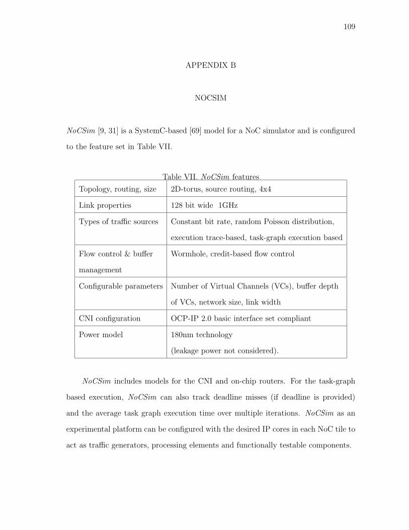
109
APPENDIX B
NOCSIM
NoCSim [9, 31] is a SystemC-based [69] model for a NoC simulator and is configured
to the feature set in Table VII.
Table VII. NoCSim features
Topology, routing, size 2D-torus, source routing, 4x4
Link properties 128 bit wide 1GHz
Types of traffic sources Constant bit rate, random Poisson distribution,
execution trace-based, task-graph execution based
Flow control & buffer Wormhole, credit-based flow control
management
Configurable parameters Number of Virtual Channels (VCs), buffer depth
of VCs, network size, link width
CNI configuration OCP-IP 2.0 basic interface set compliant
Power model 180nm technology
(leakage power not considered).
NoCSim includes models for the CNI and on-chip routers. For the task-graph
based execution, NoCSim can also track deadline misses (if deadline is provided)
and the average task graph execution time over multiple iterations. NoCSim as an
experimental platform can be configured with the desired IP cores in each NoC tile to
act as traffic generators, processing elements and functionally testable components.

110
VITA
Praveen Bhojwani was born in Sharjah, United Arab Emirates (U.A.E.). After
completing his schooling at The Modern High School, Dubai, U.A.E., he went on to
obtain his Bachelor of Technology (Honors) in computer science and engineering at
the Indian Institute of Technology (IIT), Kharagpur, India, in May 2001. He grad-
uated with his Master of Science degree in computer engineering from Texas A&M
University, College Station, Texas in December 2003.
Permanent Address:
A/41 Archana Co-op. Housing Society,
New Versova Link Road,
Andheri (W),
Mumbai 400 053,
Maharashtra,
India.
The typist for this thesis was the author.