
Communication Microelectronics ELCT508 (W17)eee.guc.edu.eg/Courses/Electronics/ELCT508...
28
Communication Microelectronics ELCT508 (W17) Lecture 5: Analysis of BJT Amplifiers Dr. Eman Azab Assistant Professor Office: C3.315 E-mail: [email protected] Dr. Eman Azab Electronics Dept., Faculty of IET The German University in Cairo 1
Transcript of Communication Microelectronics ELCT508 (W17)eee.guc.edu.eg/Courses/Electronics/ELCT508...
Communication Microelectronics ELCT508 (W17)
Lecture 5: Analysis of BJT AmplifiersDr. Eman Azab
Assistant Professor
Office: C3.315
E-mail: [email protected]
Dr. Eman Azab Electronics Dept., Faculty of IETThe German University in Cairo
1

BJT Modes of OperationElectrical Equations of BJT
Dr. Eman AzabElectronics Dept., Faculty of IETThe German University in Cairo
2

BJT NPN Modes of Operation
Dr. Eman AzabElectronics Dept., Faculty of IETThe German University in Cairo
3
Mode BEJ BCJ Equations Condition
Cutoff Reverse Reverse 𝐼𝐶 = 𝐼𝐸 = 𝐼𝐵=0𝑉𝐵𝐸 < 0.7𝑉𝐵𝐶 < 0.5
Active (Forward)
Forward
Reverse
𝑉𝐵𝐸 = 0.7𝐼𝐸 = 𝐼𝐶 + 𝐼𝐵
𝐼𝐶 = 𝛽𝐹𝐼𝐵 = 𝛼𝐹𝐼𝐸
𝛼𝐹 =𝛽𝐹
1 + 𝛽𝐹
𝑉𝐵𝐶 < 0.5Or
𝑉𝐶𝐸 > 0.2
SaturationForward
Forward
𝑉𝐵𝐸 = 0.7𝑉𝐵𝐶 = 0.5𝑉𝐶𝐸 = 0.2𝐼𝐸 = 𝐼𝐶 + 𝐼𝐵
𝐼𝐶 < 𝛽𝐹𝐼𝐵
Reverse Active
Reverse
Forward
𝑉𝐵𝐶 = 0.5𝐼𝐶 = 𝐼𝐸 + 𝐼𝐵
𝐼𝐸 = 𝛽𝑅𝐼𝐵 = 𝛼𝑅𝐼𝐶
𝛼𝑅 =𝛽𝑅
1 + 𝛽𝑅
𝑉𝐵𝐸 < 0.7Q
Q

BJT Large Signal Model in Active Mode
Dr. Eman AzabElectronics Dept., Faculty of IETThe German University in Cairo
4
Q

BJT Voltage AmplifiersDesign and Analysis of BJT Amplifiers
Dr. Eman AzabElectronics Dept., Faculty of IETThe German University in Cairo
5

Objective
We want to implement a voltage amplifier using BJT
What are the Specifications of an Ideal Voltage Amp.?
Infinite Input Resistance: Rin (Thevinen at the Input Ports)
Infinite Voltage Gain: Avo
Finite Output Resistance (Short Circuit): Rout (Thevinen at theOutput Ports)
Dr. Eman AzabElectronics Dept., Faculty of IETThe German University in Cairo
6
'out
vo
in
vA
v
outv
sig
vA
v
in Lv vo
sig in out L
R RA A
R R R R

Important Notes
BJT Amplifiers deals with DC and AC signals, Thus weneed to have different symbols to distinguish betweenthem
Dr. Eman AzabElectronics Dept., Faculty of IETThe German University in Cairo
7
Type of Signal Signal Symbol Example
DC SignalsCapital Letter and
Subscript VBE, VCE, IC
AC Signals (Small Signals)
Small Letter and Subscript vbe ,vce, ic
Instantaneous (Large Signals)
Small Letter and Capital Subscript vBE, vCE, iC
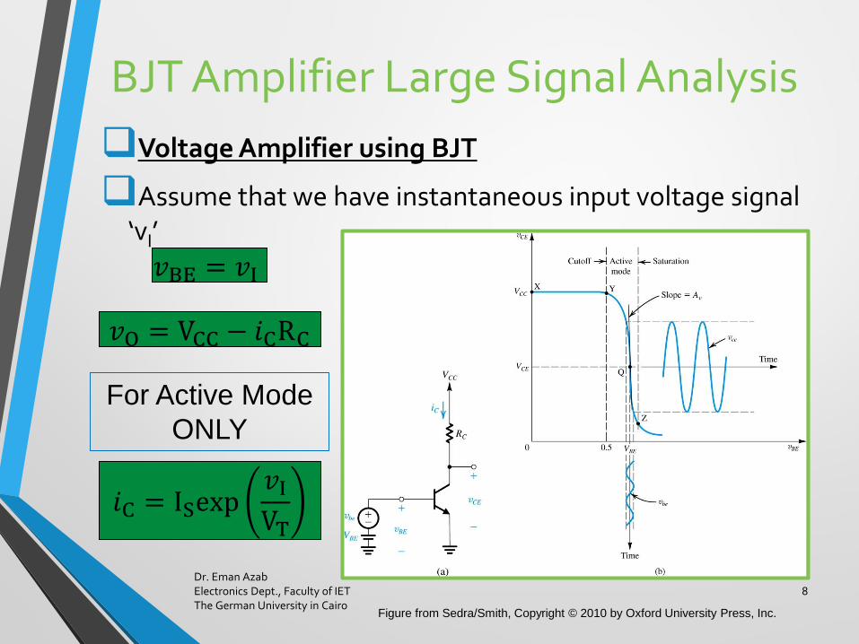
BJT Amplifier Large Signal Analysis
Voltage Amplifier using BJT
Assume that we have instantaneous input voltage signal ‘vI’
Dr. Eman AzabElectronics Dept., Faculty of IETThe German University in Cairo
8
Figure from Sedra/Smith, Copyright © 2010 by Oxford University Press, Inc.
For Active Mode
ONLY
𝑣O = VCC − 𝑖CRC
𝑖C = ISexp𝑣IVT
𝑣BE = 𝑣I

BJT Large Signal Analysis
Voltage Amplifier using BJT
1. Cutoff Mode
2. Active Mode
3. Saturation Mode
Dr. Eman AzabElectronics Dept., Faculty of IETThe German University in Cairo
9
Figure from Sedra/Smith, Copyright © 2010 by Oxford University Press, Inc.
0 ≤ 𝑣I ≤ 0.5 𝑣O = VCC
0.5 ≤ 𝑣I ≤ 𝑣BE,sat 𝑣O > 𝑣CE,sat
𝑣O = VCC − ISRCexp𝑣IVT
𝑣I ≥ 𝑣BE,sat 𝑣O = 𝑉CE,sat
𝑣O = VCC − 𝑖CRC

BJT as an Amplifier
We can easily separate DC and AC Signals (Superposition)
Under the assumption that the AC signal amplitude is very small, such that thetransistor’s mode will remain the same for the complete cycle
BJT must work in Active Mode to avoid signal distortion
DC Sources are used to set the DC Operating point to Activemode
Input terminals of the amplifier are Base/Emitter
Output terminals of the amplifier are Collector/Emitter
Equivalent Circuit for Small Signal Analysis can be derived
Dr. Eman AzabElectronics Dept., Faculty of IETThe German University in Cairo
10
𝑣BE = VBE + 𝑣𝑏𝑒 𝑖C = ISexpVBE+𝑣𝑏𝑒
VT
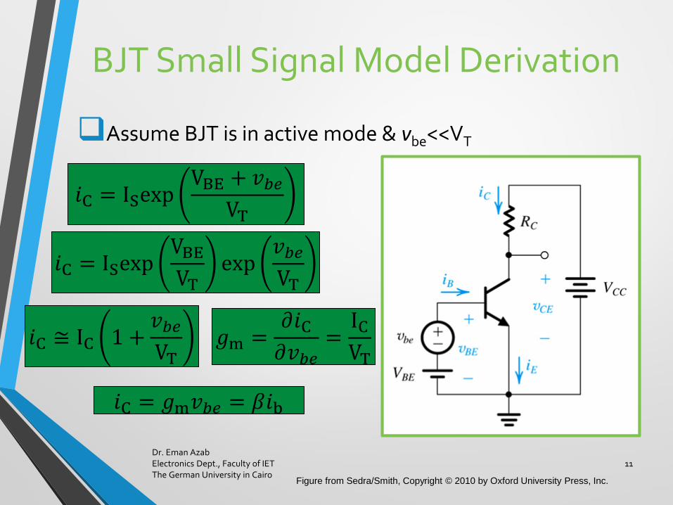
BJT Small Signal Model Derivation
Assume BJT is in active mode & vbe<<VT
Dr. Eman AzabElectronics Dept., Faculty of IETThe German University in Cairo
11
Figure from Sedra/Smith, Copyright © 2010 by Oxford University Press, Inc.
𝑖C = ISexpVBE + 𝑣𝑏𝑒
VT
𝑖C = ISexpVBEVT
exp𝑣𝑏𝑒VT
𝑖C ≅ IC 1 +𝑣𝑏𝑒VT
𝑔m =𝜕𝑖C𝜕𝑣𝑏𝑒
=ICVT
𝑖C = 𝑔m𝑣𝑏𝑒 = 𝛽𝑖b
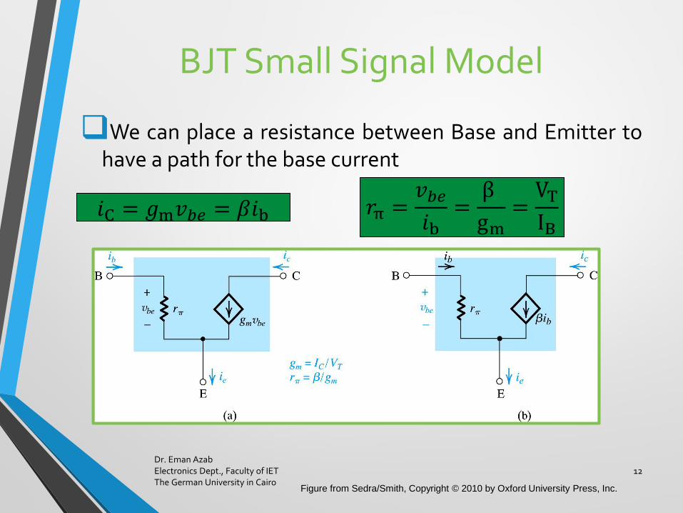
BJT Small Signal Model
We can place a resistance between Base and Emitter tohave a path for the base current
Dr. Eman AzabElectronics Dept., Faculty of IETThe German University in Cairo
12
Figure from Sedra/Smith, Copyright © 2010 by Oxford University Press, Inc.
𝑖C = 𝑔m𝑣𝑏𝑒 = 𝛽𝑖b 𝑟π =𝑣𝑏𝑒𝑖b
=β
gm=VTIB

BJT Small Signal Model
Note: Early effect can be taken into consideration (if VA
is given)
Dr. Eman AzabElectronics Dept., Faculty of IETThe German University in Cairo
13
Figure from Sedra/Smith, Copyright © 2010 by Oxford University Press, Inc.
𝑟o =VAIC
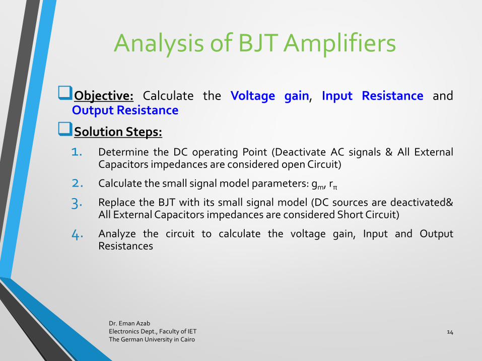
Analysis of BJT Amplifiers
Objective: Calculate the Voltage gain, Input Resistance andOutput Resistance
Solution Steps:
1. Determine the DC operating Point (Deactivate AC signals & All ExternalCapacitors impedances are considered open Circuit)
2. Calculate the small signal model parameters: gm, rπ
3. Replace the BJT with its small signal model (DC sources are deactivated&All External Capacitors impedances are considered Short Circuit)
4. Analyze the circuit to calculate the voltage gain, Input and OutputResistances
Dr. Eman AzabElectronics Dept., Faculty of IETThe German University in Cairo
14

BJT Amplifier ConfigurationsBasic Configurations and their Characteristics
Dr. Eman AzabElectronics Dept., Faculty of IETThe German University in Cairo
15
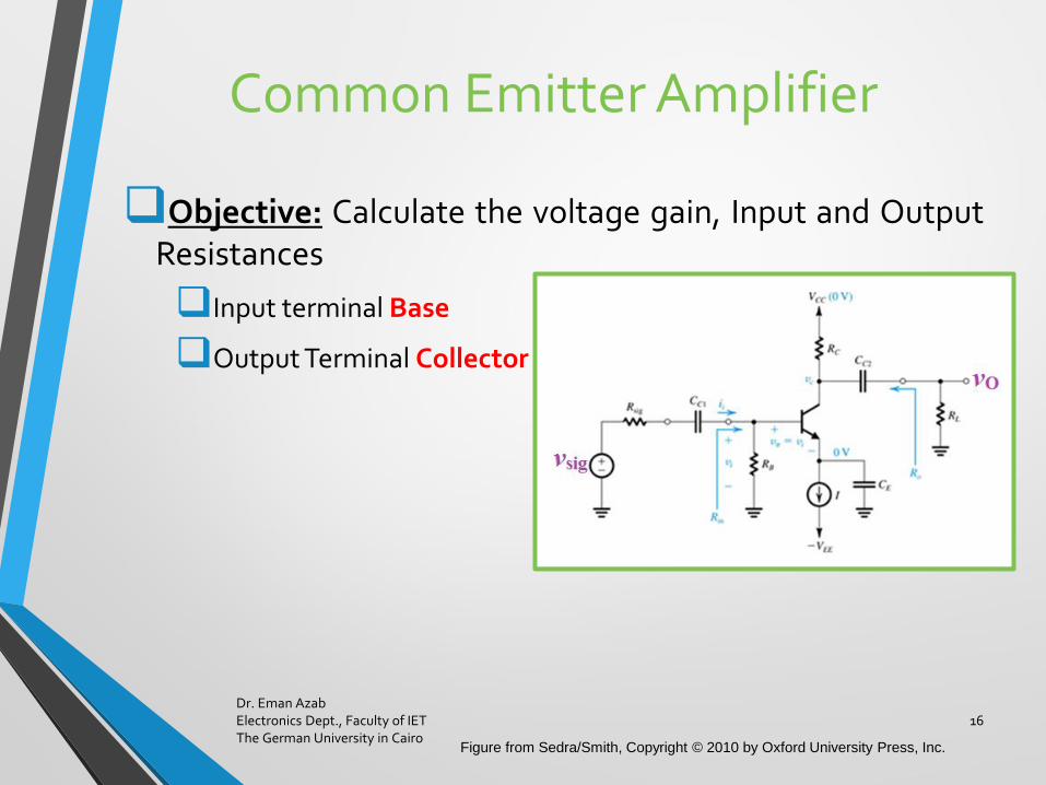
Common Emitter Amplifier
Objective: Calculate the voltage gain, Input and OutputResistances
Input terminal Base
Output Terminal Collector
Dr. Eman AzabElectronics Dept., Faculty of IETThe German University in Cairo
16
Figure from Sedra/Smith, Copyright © 2010 by Oxford University Press, Inc.

Common Emitter Amplifier
1. Calculate the DC Current
2. Calculate gm and rπ
Dr. Eman AzabElectronics Dept., Faculty of IETThe German University in Cairo
17
Figure from Sedra/Smith, Copyright © 2010 by Oxford University Press, Inc.
IC =β
1 + βI ≅ I

Common Emitter Amplifier
3. Draw the equivalent small signal model (Include ro ifgiven)
Dr. Eman AzabElectronics Dept., Faculty of IETThe German University in Cairo
18
Figure from Sedra/Smith, Copyright © 2010 by Oxford University Press, Inc.

Common Emitter Amplifier
3. Draw the equivalent small signal model (Include ro ifgiven)
4. Calculate the gain, input and output Resistance
Dr. Eman AzabElectronics Dept., Faculty of IETThe German University in Cairo
19
Figure from Sedra/Smith, Copyright © 2010 by Oxford University Press, Inc.
Av =𝑣O𝑣sig
= −gm(ro ∕∕ RC ∕∕ RL)RB ∕∕ rπ
RB ∕∕ rπ + Rsig
Rin = RB ∕∕ rπ Rout = ro ∕∕ RC ∕∕ RL
Common Emitter Amplifier
Notes on Common Emitter Configuration:
Inverting Amplifier
Gain is greater than unity
High Input Resistance
High Output Resistance
Dr. Eman AzabElectronics Dept., Faculty of IETThe German University in Cairo
20
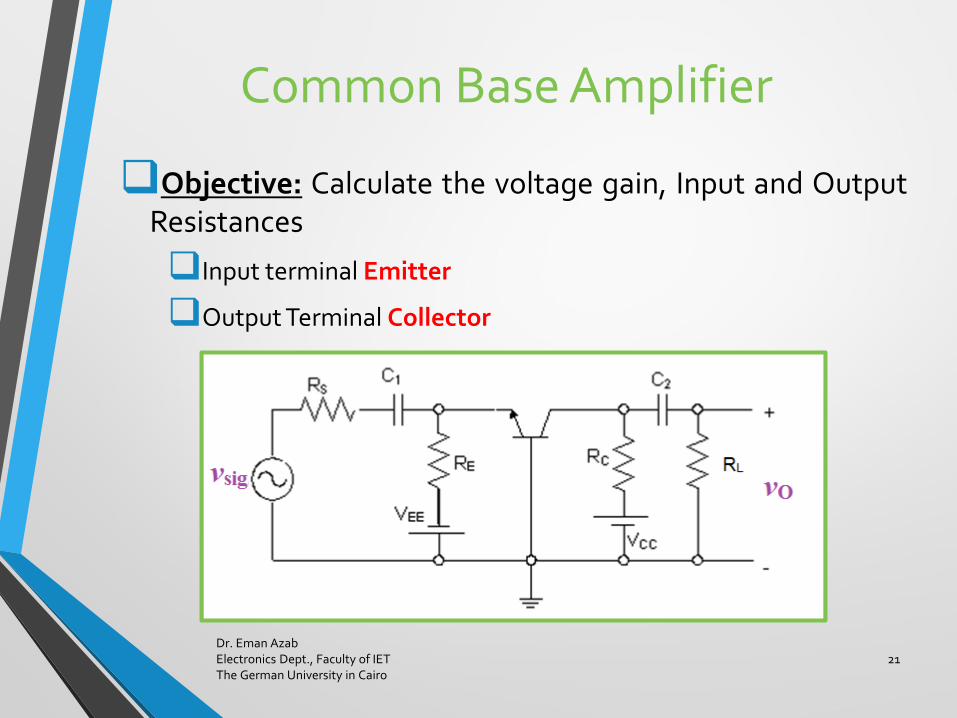
Common Base Amplifier
Objective: Calculate the voltage gain, Input and OutputResistances
Input terminal Emitter
Output Terminal Collector
Dr. Eman AzabElectronics Dept., Faculty of IETThe German University in Cairo
21

Common Base Amplifier
Voltage gain, input and Output Resistance (ro isneglected)
Dr. Eman AzabElectronics Dept., Faculty of IETThe German University in Cairo
22
Av =𝑣O𝑣sig
=gm(RC ∕∕ RL)
1 +RS
(RE ∕∕rπ
1 + β)
Rin = RS + (RE ∕∕rπ
1 + β)
Rout = RC ∕∕ RL

Common Base Amplifier
Dr. Eman AzabElectronics Dept., Faculty of IETThe German University in Cairo
23
Notes on Common Base Configuration:
Non-Inverting Amplifier
Gain is greater than unity
Low Input Resistance
High Output Resistance

Common Collector Amplifier
Objective: Calculate the voltage gain, Input and OutputResistances
Input terminal Base
Output Terminal Emitter
Dr. Eman AzabElectronics Dept., Faculty of IETThe German University in Cairo
24
Figure from Sedra/Smith, Copyright © 2010 by Oxford University Press, Inc.

Common Collector Amplifier
Voltage gain, input and Output Resistance
Dr. Eman AzabElectronics Dept., Faculty of IETThe German University in Cairo
25
Av =𝑣O𝑣sig
=1 + β (ro ∕∕ RL)
rπ + 1 + β (ro ∕∕ RL) 1 +RsigRB
+ Rsig

Common Collector Amplifier
Voltage gain, input and Output Resistance
Dr. Eman AzabElectronics Dept., Faculty of IETThe German University in Cairo
26
Rin = RB ∕∕ rπ + 1 + β ro ∕∕ RL
Rout = ro ∕∕rπ + RB ∕∕ Rsig
1 + β

Common Collector Amplifier
Dr. Eman AzabElectronics Dept., Faculty of IETThe German University in Cairo
27
Notes on Common Collector Configuration:
Non-Inverting Amplifier
Gain is less than unity
Emitter Follower (Buffer)
High Input Resistance
Low Output Resistance

Common Emitter with emitter Resistance
Dr. Eman AzabElectronics Dept., Faculty of IETThe German University in Cairo
28
Exercise:
Find the Voltage gain, input and Output Resistance
Figure from Sedra/Smith, Copyright © 2010 by Oxford University Press, Inc.


![[ Sedra] Microelectronic Circuits(b Ok.org)](https://static.fdocuments.in/doc/165x107/617b73ef7012c349660bd625/-sedra-microelectronic-circuitsb-okorg.jpg)