Common Digital Circuits - Carleton University
26
Digital Circuits © John Knight Dig Cir p. 47 Revised; October 9, 2003 Digital Circuits People don’t understand double negatives Asserted-Low (Low-True) Signals Low-true signals implement their name when low . Their names often end in “(L)” or “_N” High-true signals implement their name when high . Their names end in “(H)” or nothing. . Example: Cow feeding circuit FEED(H) is asserted high (high-true). It implements its name when high. CLK is not asserted either high or low. E G F E,G and F have no physical meaning. They are not asserted-high or asserted-low Cow feeding Logic FEED(H) CLK Slide 24 Carleton University © John Knight Digital Circuits p. 48 Revised; October 9, 2003 Digital Circuits Asserted-Low Signals Common Digital Circuits Asserted-Low Signals “The electrons have no knowledge of what meanings we attach to these signals.” (Richard Hamming) Asserted-Low (Low-True) Signals Definition These are signals which carry out the function of their name, when low. Examples FLASH_LED(L), ERROR(L) used to be prefered for schematic design. CLEAR_LATCH_N, CHIP_SELECT_N for Verilog code which cannot have brackets. b_N(7), b_N(6), . . . b_N(0) as bits of a binary number. Warning The notation “(L)” or “_N” can get very cumbersome. It is very useful for work involving block diagram interconnections or maintenance. It is very messy to do Boolean algebra on such names. Instead convert the signals to normal high-true signals to do thinking. It is very easy to use DeMorgan’s theorem to transform them back at the end. Comment on Slide 24
Transcript of Common Digital Circuits - Carleton University

Digital Circuits
© John Knight
Dig Cir p. 47 Revised; October 9, 2003
Digital CircuitsPeople don’t understand double negatives
Asserted-Low (Low-True) Signals
Low-true signals implement their name when low.Their names often end in “(L)” or “_N”
High-true signals implement their name when high.Their names end in “(H)” or nothing.
.
Example: Cow feeding circuit
FEED(H) is asserted high (high-true).It implements its name when high.
CLK is not asserted either high or low.
EG
F E,G and F have no physicalmeaning. They are notasserted-high or asserted-low
Cow feedingLogic
FEED(H)
CLK
Slide 24
Carleton University © John Knight
Digital Circuits p. 48 Revised; October 9, 2003
Digital Circuits Asserted-Low Signals
Common Digital Circuits
Asserted-Low Signals
“The electrons have no knowledge of what meanings we attach to these signals.” (Richard Hamming)
Asserted-Low (Low-True) Signals
Definition
These are signals which carry out the function of their name, when low.
Examples
FLASH_LED(L), ERROR(L) used to be prefered for schematic design.
CLEAR_LATCH_N, CHIP_SELECT_N for Verilog code which cannot have brackets.
b_N(7), b_N(6), . . . b_N(0) as bits of a binary number.
Warning
The notation “(L)” or “_N” can get very cumbersome.It is very useful for work involving block diagram interconnections or maintenance.
It is very messy to do Boolean algebra on such names. Instead convert the signals to normal high-true signals todo thinking.
It is very easy to use DeMorgan’s theorem to transform them back at the end.
Comment on Slide 24

Digital Circuits
© John Knight
Dig Cir p. 49 Revised; October 9, 2003
Asserted-Low Signals (cont.)
• Change the signal name to STARVE(L)
• Convention places an where a low-true signalenters or leaves a circuit block.
• This only reinforces the low-true naming.The physical circuit is unchanged!
• IEEE convention, used by TI and Signetics, uses arather than
• Avoids temptation to insert a real inverter for amental one.
Most Board Inputs are Asserted-Low
In TTL logic a disconnected input went high.Pulling an input plug would assert high-true inputs.
This was usually not wanted.(suppose the input fired missiles)
Thus TTL inputs were made asserted low
CMOS board designers often still use pull-ups to VDD,They then design for asserted-low
to avoid the plug pulling problem..
Such is the strength of tradition
Convert After Thinking is Done
Cow feedingLogic
STARVE_N
CLK
Cow feedingLogicCLK
BETTER
STARVE_N
+VDD
LAUNCH(L)
Slide 25
Carleton University © John Knight
Digital Circuits p. 50 Revised; October 9, 2003
Digital Circuits Asserted Low Conventions
Comment on Slide 25
Digital Circuits
Asserted Low Conventions• Any asserted low signal entering a block (not a gate) type symbol has an inverting symbol
or better where it enters the block.
• Then mentally, all signals are asserted high inside the block as a symbol.When ENABLE_N=0, EN inside the box symbol is true,and the chip is enabled.
• Since the conversion ENABLE_N=0, to an asserted-high EN inside the block is only mental, the is abetter symbol, but it is so seldom used it may cause more confusion than it saves.
• Asserted-low output signals are analogous.
The is not used for gate-level schematics
On a schematic, a low-true signal may have to enter a gate without aor preferably one may be able to DeMorgan the gate to get an input .
•
ENABLE_N
EN
RESET_N
RESET_N

Common Circuit Blocks
© John Knight
Dig Cir p. 51 Revised; October 9, 2003
Common Circuit Blocks
Combinational Circuits1. Multiplexer (MUX)
a. Digital
b. Analog
2. DeMUX, Decoder
3. Priority Encoder
4. Barrel Rotators and Shifters
5. Adders
6. Incrementers
7. Subtracters and Two’s Complement
Descriptions Given For the Above Circuits1. Verilog
2. Circuit
Slide 26
Carleton University © John Knight
Digital Circuits p. 52 Revised; October 9, 2003
Common Circuit Blocks Common Circuit Blocks
Comment on Slide 26
Common Circuit Blocks
These blocks will be discussed in reasonable detail.

Multiplexers
© John Knight
Dig Cir p. 53 Revised; October 9, 2003
Multiplexers
Digital 2-Input MUXApplication
Symbol
IEEE symbol:
S= 0 connects b yS= 1 connects a y
Circuit
Complex Gate Circuit
SELECT1
1
1
1
SELECT
2-input
1
1
S
a
b
MUXy
S
01
Virtualsignal
11
SelectInputs
Connects
b ya y
1
1
G1/1
S
a
by
G1/1
Often shortenedto G1
S
b
+5 V
S
S
ay
S
b
a
S
b
+5 V
S S
a
yS
ba
Complex GateDetails
S
a
b
y
Sa
b
y
Slide 27
Carleton University © John Knight
Digital Circuits p. 54 Revised; October 9, 2003
Multiplexers Common Circuit Blocks
Comment on Slide 27
IEEE Symbols for a MUX
2-Input MUX
The numbers represent internal “virtual” signals. Onecould have used say 7 instead of 1.
A G1 stands for “Gate” (AND) input present signal Swith a virtual signal 1 from some other point in thecircuit.
A G1 means Gate with signal 1 when this line is low.
The G1/1 means Gate with signal 1 when this line ishigh and with 1 when it is low.
It is usual to assume the 1 for a MUX and just write G1.
The word MUX at the top shows the circuit combinesthese gated inputs like a MUX.
The IEEE standard does not retain the shaped gates.They put everything in rectangles.
1
1G1
S
a
b
MUX
S
a 1
1
1G1/1
S
a
b
MUX 7
7G7/7
S
a
b
MUX
1
1G1/1
S
a
b
MUX
1G1
S
b
MUX
1
G1S
a MUX
S
b 1
G1
S
b
a 1
1
1
1
G1
a
b
MUX
y
S
y
y
y y
y
y

Multiplexers
© John Knight
Dig Cir p. 55 Revised; October 9, 2003
Digital 2-Input MUX (cont.)
VerilogBehavioural Description
Uses Conditional operator
If Cond ? True: False;
//Verilog MUX//Using Structual If
m
wire y; //outputwire a, b, S; //inputs: control
assign y = (S) ? a: b;
Sy
1
1aa
Slide 28
Carleton University © John Knight
Digital Circuits p. 56 Revised; October 9, 2003
Multiplexers 2-Input Mux
Comment on Slide 28
2-Input MuxA 2-input MUX is perhaps easiest to write this way.
Multiplexers
© John Knight
Dig Cir p. 57 Revised; October 9, 2003
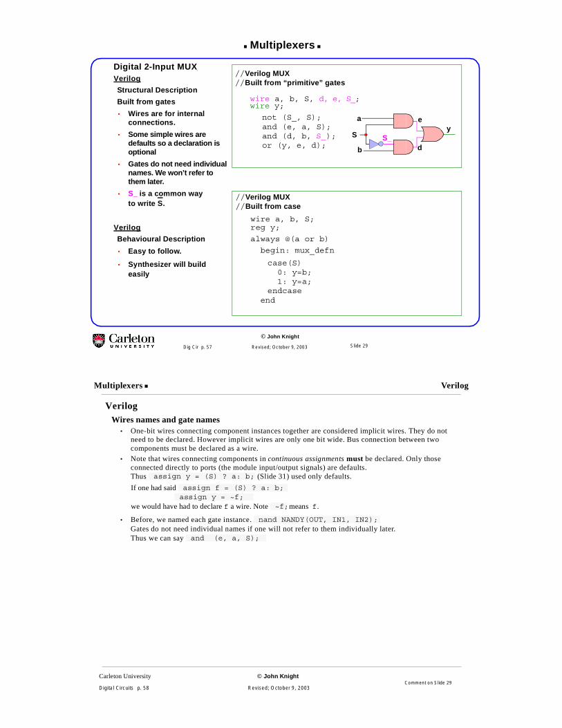
Digital 2-Input MUXVerilog
Structural Description
Built from gates
• Wires are for internalconnections.
• Some simple wires aredefaults so a declaration isoptional
• Gates do not need individualnames. We won’t refer tothem later.
• S_ is a common wayto write S.
Verilog
Behavioural Description
• Easy to follow.
• Synthesizer will buildeasily
//Verilog MUX//Built from “primitive” gates
wire a, b, S, d, e, S_;wire y;
not (S_, S);and (e, a, S);and (d, b, S_);or (y, e, d);
S
a
b
e
dS_
y
//Verilog MUX//Built from case
wire a, b, S;reg y;
always @(a or b)
begin: mux_defn
case(S)0: y=b;1: y=a;
endcaseend
Slide 29
Carleton University © John Knight
Digital Circuits p. 58 Revised; October 9, 2003
Multiplexers Verilog
Comment on Slide 29
VerilogWires names and gate names
• One-bit wires connecting component instances together are considered implicit wires. They do notneed to be declared. However implicit wires are only one bit wide. Bus connection between twocomponents must be declared as a wire.
• Note that wires connecting components in continuous assignments must be declared. Only thoseconnected directly to ports (the module input/output signals) are defaults.Thus (Slide 31) used only defaults.
If one had said
we would have had to declare f a wire. Note means f.
• Before, we named each gate instance.Gates do not need individual names if one will not refer to them individually later.Thus we can say
assign y = (S) ? a: b;
assign f = (S) ? a: b;assign y = ~f;
~f;
nand NANDY(OUT, IN1, IN2);
and (e, a, S);

Multiplexers
© John Knight
Dig Cir p. 59 Revised; October 9, 2003
Transmission Gates; a Switch of TransistorsFor Low Channel Resistance, One Needs a Large Gate-to-Channel Voltage
+5 V
G
VCHAN ≈ 0V
NMOS
NMOS can pass low voltages
+5 V
VCHANNEL≈ 5V
|VG-CHAN|
RE
SIS
TAN
CE
PMOS
PMOS can pass high voltages
R
+5 V
VOUT
LOAD
but not low ones. but not high ones.
4321
5
0
Lo
∞
G
VG-CHAN
RE
SIS
TAN
CE
4321
5
0
Lo
∞
Threshold
With both PMOS and NMOS, can both Hi and Lo.
VIN
VIN
PMOS-RONNMOS-RON
TOTAL-RON
0 5
RON
Slide 30
Carleton University © John Knight
Digital Circuits p. 60 Revised; October 9, 2003
Multiplexers Verilog
Comment on Slide 30
Conducting Transistors
In order for a transistor channel to conduct well, the gate voltage must be much higher than the channel voltage
Substrate Connection For Transmission Gates
The substrate must be connected to the lowest voltage, probably ground, for NMOS andthe highest voltage, probably VDD for PMOS.Otherwise the channel-substrate diode becomes forward biased.
PN+N+
SOURCEDRAINGATE
The gate voltage attracts carriers toform a thin layer under the oxide. Theymake a channel between N+ and N+A high gate voltage attracts more carriersand gives lower on resistance.Channel under the
thin oxide.
(c)
VDD
PMOS
NMOS

Multiplexers
© John Knight
Dig Cir p. 61 Revised; October 9, 2003
Analog MUXTransmission Gate
• The gate and two symbols
Transmission Gate Mux
• Very small 6 transistor circuit.
• Does not invert.
• Transmission gates add extra resistanceand hence delay.
• Parallel transistors are hard to test.The circuit still partially works if one isopen.
Analog Signals
• The circuit will switch analog signals, but - - -If a and b go negative, your channel-substrate junction will become forward biased.
MUX is Bidirectional
• Do not drive buses through a transmission gate.A high powered bus may feed backwards throughthe gate and overpower weaker logic.
VCNTRL
VIN VOUT VIN
VCNTRL
VOUT
VCNTRL
VIN VOUT
SEL
a
b
1
1
X1/1
SEL
b
a
MUXy y
IEEE SYMBOLCIRCUIT
SEL
A bit of artistic
license
VCNTRL BUS
1DC1
Weak D-ff contains transmission gates
Slide 31
Carleton University © John Knight
Digital Circuits p. 62 Revised; October 9, 2003
Multiplexers Verilog
Comment on Slide 31
Analog MUX
The Transmission Gate
On and Off
The Analog MUX
The IEEE Symbol• The letter G on the digital MUX is replaced by X. G stood for gated, indicated an ANDing of two leads.
X is a bidirectional gateing. The analog MUX can work in either direction.
• The double arrows show the signals can travel either way.
Advantages• This MUX is very simple, replacing 10 or 12 transistors in the gate built MUX, with 6 or 8. The larger
number in each case is for an inverter at the output.
• The MUX does not invert. However most MUX standard cells will add an inverter an output buffer..
Disadvantages• This MUX adds an extra resistance in the signal path. Remember the delay has a component that
increases quadraticly with the number of series transistors (Comment on Slide 14). Check if the gatesdriving a or b have three or more series gates already.
• Suppose one of the parallel transistors in a transmission gate is no good. The other one will still conduct albeit with ahigher resistance and a possible threshold drop. Capacitances may be half charged and give erratic results.1 Manycircuit will work but more slowly. Testing for slow response, delay testing, is much harder than normal static testing.
Testing for static power supply current, IDDQ testing, can sometimes find partial charges on capacitors, since thesemay allow a direct path from VDD to ground. This is changing the present attitude toward transmission gates.
1. Thomas DeMassa and Zack Ciccone, Digital Integrated Circuits, John Wiley, 1996, p.432.
VCNTRL=1 VCNTRL= 0
1
0
0
1
OFFON

Multiplexers
© John Knight
Dig Cir p. 63 Revised; October 9, 2003
4-Input MUXThe IEEE symbol
decodes the 2-bit numberS1S0 into 4 virtual controlsignals.
The Circuit
36 transistor CMOScircuit.
Verilog
l = bitwise OR
& = bitwise AND
~ = bitwise NOT
Consider:
4-input
01 G0
3
MUX
0123
abcd
S0S1
y
S1 S0
21 20
00
0101
11
Virtualsignal
0123
WeightSelectInputs
Connects
a yb yc yd y
S0
c
d
y
a
b
S1
6+4
6
6
6
8
36 transistors(28 as a complex gate)
//Verilog 4-Input MUX//
wire a, b, c, d;wire S1, S0, y;
assign y = (~S1 & ~S0 & a)| // virtual sig 0(~S1 & S0 & b)| // virtual sig 1( S1 & ~S0 & c)| // virtual sig 2( S1 & S0 & d; // virtual sig 3
// Good for mental exerciseassign y =
S1 ? (S0 ? d : c ): (S0 ? b : a) ;
Slide 32
Carleton University © John Knight
Digital Circuits p. 64 Revised; October 9, 2003
Multiplexers Verilog 4-Input Mux
Verilog 4-Input Mux
Verilog
The integer 2 is translated into 10{S1,S0} says concatenate bits together.
%d says display {S1,S0} as a decimal.
4-input
01 G0
3
MUX
0123
abcd
S0S1
y
S1 S0
00
0101
11
Virtualsignal
0123
SelectInputs
Connects
a yb yc yd y
S0
c
d
y
a
b
S1
6+4
6
6
6
8
//Verilog 4-Input MUX
wire a, b, c, d;wire S1, S0,reg y;
always @ (a or b or c or d or S1 or S0);case({S1,S0})0: y=a;1: y=b;2: y=c;3: y=d;
default: $display(“Bad input %d to 4-input mux”, {S1,S0})
endcase
Comment on Slide 32n

Demultiplexers, Decoders
© John Knight
Dig Cir p. 65 Revised; October 9, 2003
Demultiplexers, Decoders
DecoderApplication
Decode 2-bit binaryinto 1-out-of-4.
Select one of the 64Kmemory blocks.
CS = chip select
Symbol
IEEE symbols:
The DeMuX and Decode areexactly the same.
The decode thinks of the yinput as an enable.
if y=0 all outputs=0
Other decoder symbolOne code inAnother code out.
Σ (nonzero inputs) tellswhich outputs are true.
12
X/1-of-40123
S0S1
A19A18A17A16
. . . . .
. . . . .A1A0 3FFFF-00000
FFFFF-C0000
BFFFF-80000
7FFFF-40000
CS
CS
CS
CS
Address Bus
64KM
EM
BL
OC
KS
µ C
OM
PU
TER
01 G
07
DMUX
0123
abcd
S0S1
Decode
2
4567
efgh
S2
E En
Decode
12
X / OCT
3-bit binary to1-out-of-8
0123
abcd
4567
efgh
S0S1
S2 4E En
01 G
07
DMUX
0123
abcd
S0S1
y
DeMUX
2
4567
efgh
S2
If inputs 2 and 4 are true, output 2+4=6 will be true.
2+4
Slide 33
Carleton University © John Knight
Digital Circuits p. 66 Revised; October 9, 2003
Demultiplexers, Decoders The DeMUX/Decoder
The DeMUX/DecoderDecoding the memory bank
Only one of the 4 blocks is selected at any given time.The 18 low-order address lines go to all blocks, but only one is enabled.
IEEE symbolsThe official convention does not shape the gates.
X/ means some code usually binary.
The output lines that are true are calculated from the sum of the numbersof the input lines.If input “1”=1, “2”=0, “4”=1, Then output line “1”+”4”= 5 would be 1.If input “1”=0, “2”=1, “4”=1, Then output line “2”+”4”= 6 would be 1.
The Enable line (En) must be 1 or all outputs are 0.
12
X / OCT
1+4
0123
0000
4567
0100
41 En
01
1
12
X / OCT
2+4
0123
0000
4567
0010
41 En
10
1
Comment on Slide 33

Demultiplexers, Decoders
© John Knight
Dig Cir p. 67 Revised; October 9, 2003
Verilog DecoderProcedural Verilog for a 3-to-8 Decoder
wire S2, S1, S0, E;reg a, b, c, d, e, f, g, h;//they hold their values like variables in C
always @(S2orS1orS0orE)//execute code below if any of S2,S1,S0 or E change
begin: 3to8decode //Start of procedure code
a=0; b=0; c=0; d=0; e=0; f=0; g=0; h=0;
case ({S2,S1,S0})//Concatenate the 3 bits into a number used below.
3'd0 : a=E; // When S2S1S0 = 0 decimal (000 binary), make a = E.3'd1 : b=E; // 3'd1; a 3-bit number, value in decimal is 1.3'd2 : c=E; // When S2S1S0 = 2 decimal (010 binary), make c = E.3'd3 : d=E;3'd4 : e=E;3'd5 : f=E;3'd6 : g=E;3'd7 : h=E;default: $display(“invalid control code”);
endcase
end //End of procedure code
endmodule
DMUX
0123
abcd
S0S1
4567
efgh
S2
E En
01 G
07
2
Slide 34
Carleton University © John Knight
Digital Circuits p. 68 Revised; October 9, 2003
Demultiplexers, Decoders Verilog Decoder
Verilog Decoder
Comment on Slide 34
Priority Encoders
© John Knight
Dig Cir p. 69 Revised; October 9, 2003
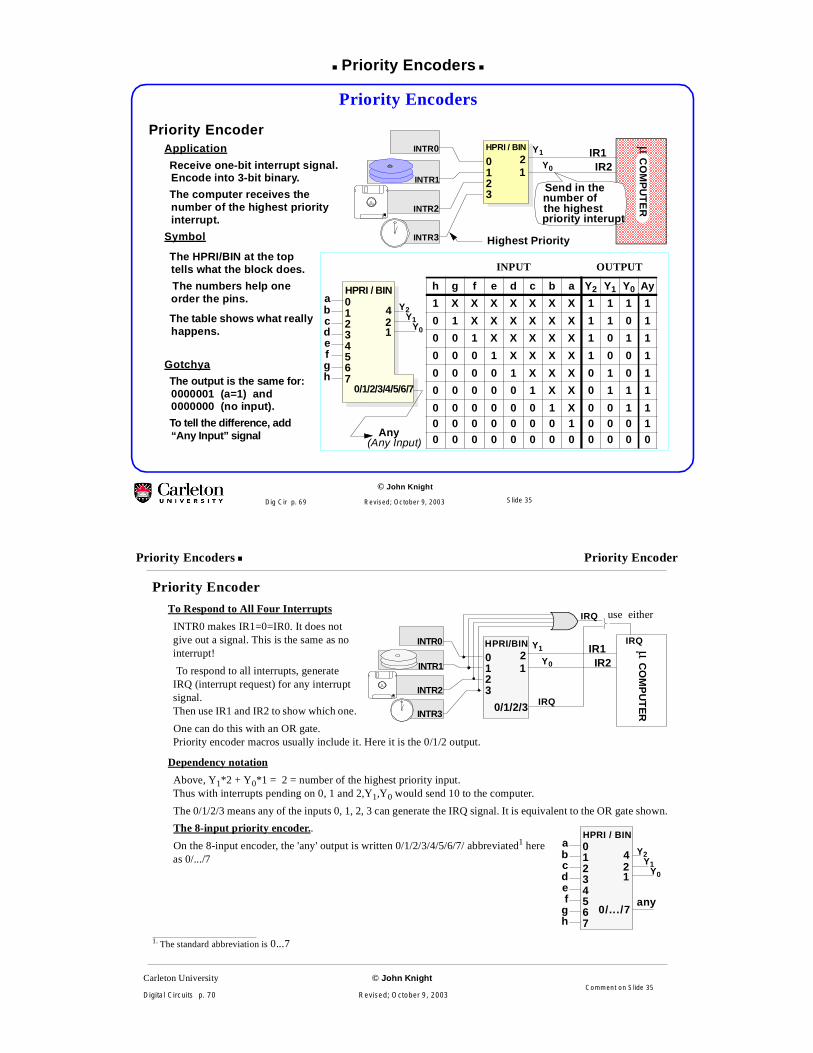
Priority Encoders
Priority EncoderApplication
Receive one-bit interrupt signal.Encode into 3-bit binary.
The computer receives thenumber of the highest priorityinterrupt.
Symbol
The HPRI/BIN at the toptells what the block does.
The numbers help oneorder the pins.
The table shows what reallyhappens.
Gotchya
The output is the same for:0000001 (a=1) and0000000 (no input).
To tell the difference, add“Any Input” signal
21
HPRI / BIN
0123
Y0
Y1 IR1IR2
INTR0
INTR1
INTR2
INTR3 Highest Priority
µ CO
MP
UT
ER
Send in thenumber ofthe highestpriority interupt
12
HPRI / BIN0123
abcd
4567
efgh
Y0
Y1
Y24
INPUT OUTPUT
h g f e d c b a Y2 Y1 Y0 Ay
1 X X X X X X X 1 1 1 1
0 1 X X X X X X 1 1 0 1
0 0 1 X X X X X 1 0 1 1
0 0 0 1 X X X X 1 0 0 1
0 0 0 0 1 X X X 0 1 0 1
0 0 0 0 0 1 X X 0 1 1 1
0 0 0 0 0 0 1 X 0 0 1 10 0 0 0 0 0 0 1 0 0 0 10 0 0 0 0 0 0 0 0 0 0 0
0/1/2/3/4/5/6/7
Any(Any Input)
Slide 35
Carleton University © John Knight
Digital Circuits p. 70 Revised; October 9, 2003
Priority Encoders Priority Encoder
Priority Encoder
To Respond to All Four Interrupts
INTR0 makes IR1=0=IR0. It does notgive out a signal. This is the same as nointerrupt!
To respond to all interrupts, generateIRQ (interrupt request) for any interruptsignal.Then use IR1 and IR2 to show which one.
One can do this with an OR gate.Priority encoder macros usually include it. Here it is the 0/1/2 output.
Dependency notation
Above, Y1*2 + Y0*1 = 2 = number of the highest priority input.Thus with interrupts pending on 0, 1 and 2,Y1,Y0 would send 10 to the computer.
The 0/1/2/3 means any of the inputs 0, 1, 2, 3 can generate the IRQ signal. It is equivalent to the OR gate shown.
The 8-input priority encoder..
On the 8-input encoder, the 'any' output is written 0/1/2/3/4/5/6/7/ abbreviated1 hereas 0/.../7
1. The standard abbreviation is 0...7
21
HPRI/BIN
0123
Y0
Y1 IR1IR2
INTR0
INTR1
INTR2
INTR3
µ CO
MP
UT
ER
IRQ
0/1/2/3 IRQ
IRQ use either
12
HPRI / BIN0123
abcd
4567
ef
gh
Y0
Y1
Y24
0/.../7any
Comment on Slide 35

Priority Encoders
© John Knight
Dig Cir p. 71 Revised; October 9, 2003
Verilog Priority Encoder/ Use of CasexProcedural Verilog for an 8-line to 3-Bit-Binary Encoder
reg anyreg [2:0] Y; //reg hold their values like variables in C++
always @(h or g or f or e or d or c or b or a)//trigger variables for code.
begin //Start of procedure code
casez ({h,g,f,e,d,c,b,a}) //Casez prefered over casex.
8'b1zzzzzzz : Y= 3'b111;// z will match 0 or 1 or x ( undefined).8'b01zzzzzz : Y= 3'b110;// But x will not match 0 or 1 with casez8'b001zzzzz : Y= 3'b101;8'b0001zzzz : Y= 3'b100;8'b00001zzz : Y= 3'b011;8'b000001zz : Y= 3'b010;8'b0000001z : Y= 3'b001;8'b00000001 : Y= 3'b000;default : Y= 3'b000;
endcase
any = a | b | c | d |e | f | g | h;
end //End of procedure code
0123
abcd
4567
efgh any
12
HPRI / BIN
Y0
Y1
Y24
0/1/2/3/4/5/6/7
Slide 36
Carleton University © John Knight
Digital Circuits p. 72 Revised; October 9, 2003
Priority Encoders Verilog Priority Encoder
Verilog Priority EncoderCase, Casex and Casez
Case
The values stored in the control_var and those in each statementbelow it, must agree “ 1 for 1,” “0 for 0,” “x for x,” and “z for z.”
Casez1
If , is used instead of , “z” or “?” will match anything, i.e. “1, 0, x, or z,” in both directions.The important point is a “1” or a “0” WILL NOT match an “x”.Thus control_var = 3'bz01 will match the case 3'b101 on line 2 above.Also control_var = 3'bx01 will NOT match the case 3'b101.
Casex
If , is used instead of
, “x”, “z” will match anything, i.e. “1, 0, x, or z,” in both directions.
Several cases, one action
Place several cases on one line 3'b101, 3'b010: . . . . Separate the cases by commas.
Using “?”
The “?” is equivalent to Z in list of cases inside case blocks. It improves readability.
1.• PROBLEM
Add an “Any Input” output line to the Verilog priority encoder description that uses casez.
1. Using casez instead of casex for the priority encoder, and useingstatements like 3'b1zz for matching, makes no difference forsynthesis, but an accidental X during simulation will never give an unintended for match for a 1 or a 0.
casez(control_varb)3'b101, 3'b010 : . .3'b1z1 : . . .
default : . . .
3'b0zx : . . .
end case
21
3
56
43'b1??
7
casez; case
casex
case
Comment on Slide 36

Programmable Shifters
© John Knight
Dig Cir p. 73 Revised; October 9, 2003
Programmable Shifters
Barrel Rotators (Shifters)Applications
Multiply/Divide by 2, 22, 23 ...
Normalizing numbersespecially integer to float pt.conversion.
Not CMOS
• First thought: transmissiongates.
• Big shifter takes a lot ofarea. Speed dominated bywiring capacitance.
• To reduce area have onlyone well.� no PMOS.
• NMOS can only pull up toVDD-VTHRESH
• Slow pull upFaster pull down
X3
X2
X1
X0
Y3
Y2
Y1
Y0
ROTATE RIGHT 0
ROTATE RIGHT 1
ROTATE RIGHT 2ROTATE RIGHT 3
Slide 37
Carleton University © John Knight
Digital Circuits p. 74 Revised; October 9, 2003
Programmable Shifters The Barrel Rotator
The Barrel Rotator
NMOS or CMOS
A 32 bit barrel has 322 cells. There is little room for the extra wells (tubs) required for PMOS and NMOS1.Usually only NMOS is used.
The NMOS gates can only pull up VDD -VTHRESH and some speed or leakage power is sacrificed.
Speed
There is only one series transistor in any path; this helps speed. Each data line will see n drain capacitanceswhich will reduce speed. However in modern processes the wire capacitance is likely larger than the draincapacitances. This is an important reason for using only NMOS to reduce the area.
Also zeros will go through NMOS transistors better than ones.
Verilog Synthesis
Synthesizers will not produce a very good barrel shifter, since the would try to synthesize gate level CMOS.Try to find a shifter already laid out.
Sign Extension
A negative 2’s complement number will have one as its most significant bit. If one shifts todivide by 2, 4 ..., one must move a 1 in from the right for negative numbers and a 0 in forpositive ones. This is called sign extension.
Thus 100 right shifted 1 positions is 110.A bigger number; 100100100 right shifted 3 positions is 111100100
1. Wayne Wolf, Modern VLSI Design, A Systems Approach, Prentice Hall, 1994, pp. 221-223.
2’s complement+3 011+2 010+1 001
0 000-1 111-2 110-3 101-4 100
Comment on Slide 37

Programmable Shifters
© John Knight
Dig Cir p. 75 Revised; October 9, 2003
Barrel Rotator With Weak Pullups• Weak pullups
overcome NMOSpoor pullupproperties.
• Shifter is still areasonable size.
X3
X2
X1
X0
Y3
Y2
Y2
Y0
ROT RT 0
ROT RT 1ROT RT 2
ROT RT 3
W0
W1
W2
W3
Weak Pullups
Slide 38
Carleton University © John Knight
Digital Circuits p. 76 Revised; October 9, 2003
Programmable Shifters The Barrel Rotator
Pull-Ups for the Barrel Shifter.
• The PMOS transistors will pull-up the barrel shifter NMOS transistors.When a WK lines rise above VDD/2 the PMOS transistors will turn on. This raises the WK line, whichlowers the PMOS gate, which raises the WK line, which ...
• When an X input was high, and then goes low, the PMOS will still be initially pulling up.The PMOS transistor must be made weak enough that the NMOS transistor can pull point W below halfway when both transistors are on.
• The complete shifter is much smaller than a complete CMOS implementation would be.
Why does not one make all CMOS that way?
The Wk lines in the barrel shifter are never floating. They are fed by pass transistors which either pull them low,or pull them high. Of course the high is always a threshold or more below VDD.
If CMOS gates had only a single transistor PMOS section, it could not pull up unless the W line was partiallyhigh already. If the W line was pulled low, when the NMOS transistors turned off, the W lines would stay low,held by the charge on the stray capacitance, and the Z line would stay high.
S
b
+5 V
S
aW Z
Go high and stay high circuit
Comment on Slide 38

Programmable Shifters
© John Knight
Dig Cir p. 77 Revised; October 9, 2003
Verilog rotator/shiftersSynthesis
Synthesis will not give the NMOS circuits described.
You must have a laid-out circuit which can be treatedas a special module.
If R is a variable, the synthesizer may not likeX>>R or {X[R:0],X[N:R-1]}.
Code For Simulation
Shifting 2's complement numbers
If the leading bit is “1”, the number is negative.The leading bit must be maintained during shifts.
Use replication for sign extension.
X
tmp={{4{X[3] } ,X}
tmp >> 2
rotate
Z
11110 = -2 in 2’s complementshift right 3 -> 11111shift left 2 -> 11000
R=2
wire [1:0] R\\Rotate R bits;wire [3:0] X,Z;
assign Z ={X[R:0],X[3:R-1]};
// Sign extension.
assign tmp={ {4{X[3]},X }/ / {4{X[3]}} = {X[3],X[3] ,X[3]X[3]}
assign Z = tmp >> Sh;
Slide 39
Carleton University © John Knight
Digital Circuits p. 78 Revised; October 9, 2003
Programmable Shifters Barrel Rotator Shifter (cont.)
Barrel Rotator Shifter (cont.)Verilog
Because of the size problem. one does not synthesize a large barrel shifter.
One would lay out the NMOS circuit rather than synthesize it from gates.
The Shift Operators
means shift W right Y places. V will be zero filled on the right.
means shift X right Y places. Z will be zero filled on the left unless it is an integer or real.
Sign Extension
A negative 2’s complement number will have one as its most significant bit. If one shifts todivide by 2, 4 . . . , one must move a 1 in from the left for negative numbers and a 0 in forpositive ones. This is called sign extension.
Thus (-4) 100 right shifted 1 position, with sign extension, is 110 (-2).A bigger number; (-220) 100100100 right shifted 3 positions is 111100100 (-28).
• Verilog right shifts do a zero fill for variables with a user defined bit width, like 7'd33.
• Right shifts do sign extension for integers or real, but not reg or wire. Aninteger is the default 32 or 64 bit word of the computer running Verilog.
Concatenation and Replication
{A,B} concatenates A and B. Thus {2'b11, 3'b001}� {5'b11001}A Concatenation of many copies of the same thing can be written, {5{X}}, instead of {X,X,X.X.X}the replication number, 5 above, must be a constant.
V= W << S
Z= X >> S
2’s complement+3 011+2 010+1 0010 000
-1 111-2 110-3 101-4 100
three-bit
Comment on Slide 39

Programmable Shifters
© John Knight
Dig Cir p. 79 Revised; October 9, 2003
The Logorithmic Barrel Shifter
COMPARISON Barrel Log Barrel
Numb transistors N2 2N·log2(N)
Numb series trans 1 log2(N)
fanout data lines N 3log2(N)
fanout control lines N N+1
Summary
Log shifter has better area esp. for large N
Speed depends on:fanoutnumber of series trans.
Log shifter wins because of lower fanout.
cumulativerotate 2
cumulativerotate 1 Rotate
0 0 0
0 1 1
1 0 2
1 1 3
X[3]
X[2]
X[1]
X[0]
Y[3]
Y[2]
Y[1]
Y[0]
cum rotate 1
cum rotate 2
X1[0]
X1[3]
Slide 40
Carleton University © John Knight
Digital Circuits p. 80 Revised; October 9, 2003
Programmable Shifters Barrel Rotator Shifter (cont.)
Size Comparison for Rotatorsinputs, n 4 8 16 32 64 128transistors, n2 16 64 256 1024 4096 16384transistors, 2nlog2(n) 16 48 128 320 768 1792
Speed ComparisonFor m transistors in series, the delay is roughly R(3C)(m(m+1)/2
m = log2(n)R is the channel resistance.C is the drain capacitance of each transistor. See Comment on Slide 14.
For the logarithmic rotator there are an average of 3 transistors at each junction.
For the standard barrel rotator the major delay is R(nC) + 2R(nC).The driver transistors for Xi see a capacitance of nC and the pass transistors see a load of nC.They are summed according to Elmore’s formula.1
For the same values of R and C, this analysis gives relative delays of:
inputs, n 4 8 16 32 64 128linear delay, (n+2n) 12 24 48 96 192 384logrithmic delay, 3m(m+1)/2 9 18 30 45 63 84
This does not include control line delay and makes some rather crude assumptions. However they indicate thelogarithmic rotator saves time as well as area.
1. See M.J.S Smith, Application -Specific Integrated Circuits, 1997,Addison Wesely, p. 280.
Comment on Slide 40

Programmable Shifters
© John Knight
Dig Cir p. 81 Revised; October 9, 2003
X[3]
X[2]
X[1]
X[0]
Y[3]
Y[2]
Y[1]
Y[0]
cumRot[1]
cumRot[2]
X1[0]
X1[3]
X2[0]
X[7]
X[6]
X[5]
X[4] X1[4]
Y[7]
Y[6]
Y[5]
Y[4]
cumRot[0]
wire [7:0] X, X1, X2, Y;
wire [3:0] cumRot;
always @(X or X1 or X2 or cumRot);
beginX1 = (cumRot[0])? X:{X[0],X[7:1]};X2 = (cumRot[1])? X1:
{X1[1:0],X1[7:2]};Y = (cumRot[2])? X2:
{X2[3:0],X2[7:5]};
end
X2[1]X1[1]
Verilog; 8-bit logrithmic shifterThis code will synthesize into 24 DEMUXs
X1[2] X2[2]
X1[7]
1
0DEMUX
G0/1cumRot[2]X1[3]
X2[1]
X2[3]
X2[3]
Slide 41
Carleton University © John Knight
Digital Circuits p. 82 Revised; October 9, 2003
Programmable Shifters Barrel Rotator Shifter (cont.)
Verilog CodeThe code shows an 8-bit logarithmic rotator.
The shift operations are fixed, 1, 2, or 4. Not variable amounts, thus the synthesizer will not have trouble.
The synthesizer will use 24 CMOS MUXs. Not the NMOS circuit shown.However the logarithmic circuit keeps the size reasonable.
The mux shown would replace the two transistors shown in red and bold.
Comment on Slide 41

Programmable Shifters
© John Knight
Dig Cir p. 83 Revised; October 9, 2003
Logarithmic Circuits in General
Examples of some circuits that can be made logarithmic• Barrel Shifter
• Comparator
• Counter
• Brent-Krung Adder(carry-chain)
General Examplen inputs
Algorithm must obey
• Area (or power) = K·nb b>1
or
Delay = f(n) f(n)>C·log2(n)
(K,C and b some constants)
• Must be able to divide circuitinto smaller blocks
• If the interconnections are not too large, one can save area or time.
• The comparator behaves like the “Example Algorithm” in the figure.
Area=n2 (must be > n1)
A=n2=4 4 4 4 4
44
4
Area=A(n-1)=28
log2(n)=3
Delay=n (must be > log2(n))
Delay=D·log2(n)=6
for n=2
for n=8
D=n=2
Example Algorithm for n=8Area=n2=64Delay=n=8
Total Area7 circuits of n=4
Slide 42
Carleton University © John Knight
Digital Circuits p. 84 Revised; October 9, 2003
Programmable Shifters Logarithmic Circuits
Logarithmic CircuitsGeneral Properties
Some circuits that perform certain functions, can be created to increase logarithmicly as the number of inputs“n” grows. The logarithmic barrel shifter has an area that increases as n·log2(n). The logarithmic comparator(next slide) has a delay that increases as log2(n).The Brent Krung adder (described in the adder section) has acarry chain in which the delay increases as log2(n).
Different growth rates as n increases
For large n, the dominate term is the only one that is important. Thus if the area of a ciruit increases likeArea = A·log(n) +B·n +Cn·log(n) +Dn2
The important term for n large enough is Dn2. However if D=0, the important term becomes Cn·log(n), etc.
For small n, one of the lower order terms may dominate if A or B have a large value,but as n increases thehigher order terms will always win out.
Interconnections
In the example, the interconnections between the small blocks are shown as single wires. Sometimes they aremore complicated, requiring many wires and logic. This interconnect cost may negate the gains from dividingthe circuit into small blocks.
Barrel RotatorLinear Area is proportional to n2
Logarithmic Area is proportional to 2nlog2(n)
Linear Delay is proportional to (3n)Logarithmic Delay is proportional to 3log2(n)(log2(n)+1)/2
Comment on Slide 42

The Logarithmic Comparator
© John Knight
Dig Cir p. 85 Revised; October 9, 2003
The Logarithmic Comparator
Basic Comparator BlockDescription of the yellow box
Compare two binary numbers
Each block compares:- two 2-bit numbers
or
- two 1-bit numbers and theresult of a previous compare.
Xb Yb Xa Ya X>Y X>Y
1 0 - - 1 0
0 1 - - 0 1
Xb= Yb 1 0 1 0
Xb= Yb 0 1 0 1
Xb= Yb 0 0 0 0
X>Y X<Y
X3 Y3 X2 Y2
X>Y X<Y
X1 Y1 X0 Y0
X3X2<Y3Y2
X3X2>Y3Y2
Xb Yb Xa Ya Xb Yb Xa Ya
Xb Yb Xa Ya
X>Y X<Y
X>Y X<Y
X3 Y3 X2 Y2
X>Y X<Y
X1 Y1
X3X2<Y3Y2
X3X2>Y3Y2
Xb Yb Xa Ya Xb Yb Xa Ya
X>Y X<Y
X0 Y0
Xb Yb Xa Ya
Logarithmic
Linear
Slide 43
Carleton University © John Knight
Digital Circuits p. 86 Revised; October 9, 2003
The Logarithmic Comparator Logarithmic Circuits
The ComparatorThe output of the comparator is a bit which acts like a new x and y
Thus X>Y means the number composed of the bits xixi-1 is larger than the number composed of bits yiyi-1.
The two bits (X>Y) and (X<Y) can be used in the next comparison.
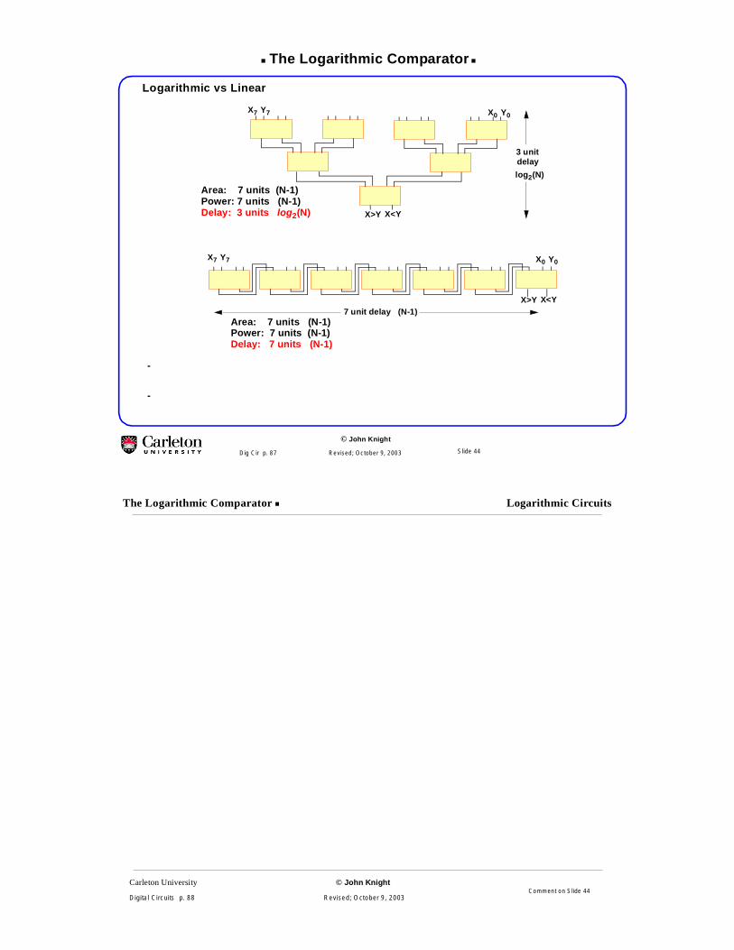
Linear vs LogarithmicDelay
For the linear comparitor, the delay increasesDelay = B·n - B
For the logarithmic comparitor the delay increasesDelay = A·log(n)
Thus one can see the logarithmic comparitor will be much faster as n gets large.
Area
There is no difference in area.
Serial inputs give different resultsHowever do not think this spells the death of the serial (linear) comparitor. Suppose the data came in seriallywith X7, Y7 coming in first and X0,Y0 coming at the end. Then the linear circuit would likely get the result outfirst because the result would come out one block delay after X0, Y0 were stable.
In the logarithmic comparitor the result has to go through log2(n) blocks after the last two input bits are stable.
Comment on Slide 43
The Logarithmic Comparator
© John Knight
Dig Cir p. 87 Revised; October 9, 2003
Logarithmic vs Linear
X>Y X<Y
X7 Y7 X0 Y0
X7 Y7 X0 Y0
X>Y X<Y
3 unitdelay
log2(N)
7 unit delay (N-1)
Area: 7 units (N-1)Power: 7 units (N-1)Delay: 3 units log2(N)
Area: 7 units (N-1)Power: 7 units (N-1)Delay: 7 units (N-1)
Slide 44
Carleton University © John Knight
Digital Circuits p. 88 Revised; October 9, 2003
The Logarithmic Comparator Logarithmic Circuits
Comment on Slide 44

The Logarithmic Comparator
© John Knight
Dig Cir p. 89 Revised; October 9, 2003 Slide 45
Carleton University © John Knight
Digital Circuits p. 90 Revised; October 9, 2003
The Logarithmic Comparator Logarithmic Circuits
Comment on Slide 45

The Logarithmic Comparator
© John Knight
Dig Cir p. 91 Revised; October 9, 2003 Slide 46
Carleton University © John Knight
Digital Circuits p. 92 Revised; October 9, 2003
The Logarithmic Comparator Logarithmic Circuits
Comment on Slide 46

The Logarithmic Comparator
© John Knight
Dig Cir p. 93 Revised; October 9, 2003 Slide 47
Carleton University © John Knight
Digital Circuits p. 94 Revised; October 9, 2003
The Logarithmic Comparator Logarithmic Circuits
Comment on Slide 47

The Logarithmic Comparator
© John Knight
Dig Cir p. 95 Revised; October 9, 2003 Slide 48
Carleton University © John Knight
Digital Circuits p. 96 Revised; October 9, 2003
The Logarithmic Comparator Logarithmic Circuits
Comment on Slide 48

The Logarithmic Comparator
© John Knight
Dig Cir p. 97 Revised; October 9, 2003 Slide 49
Carleton University © John Knight
Digital Circuits p. 98 Revised; October 9, 2003
The Logarithmic Comparator Logarithmic Circuits
Comment on Slide 49