COMMODORE SEMICONDUCTOR 73 DE| 22^4173...
19
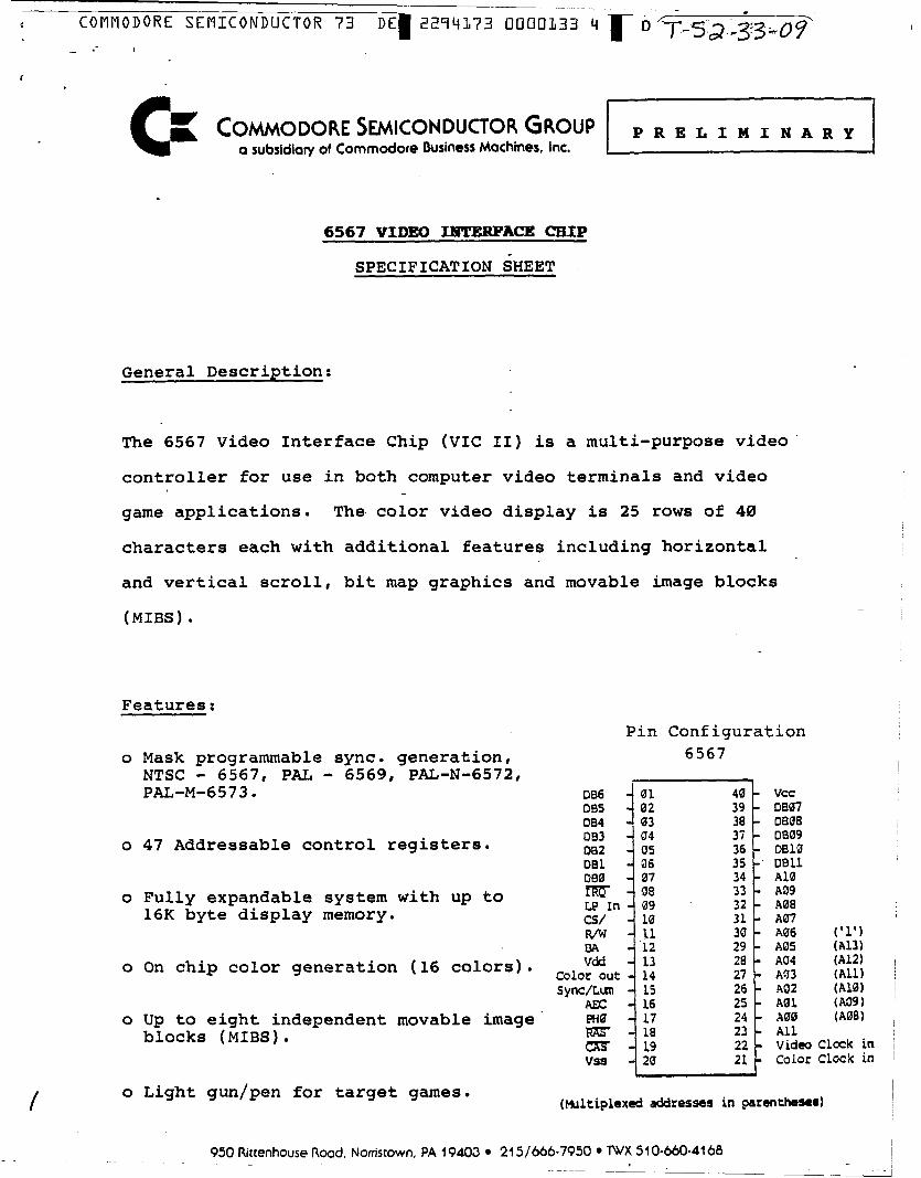
COMMODORE SEMICONDUCTOR 73 DE| 22^4173 0000133 4 D ~33~09 c = C ommodore S emiconductor G roup q subsidiary of Commodore Business Machines, Inc. 6567 VIDEO IHTKRFACE CHIP SPECIFICATION SHEET General Description; The 6567 Video Interface Chip (VIC II) is a multi-purpose video controller for use in both computer video terminals and video game applications. The color video display is 25 rows of 40 characters each with additional features including horizontal and vertical scroll, bit map graphics and movable image blocks (MIBS). Features: o Mask programmable sync, generation, NTSC - 6567, PAL - 6569, PAL-N-6572, PAL-M-6573. o 47 Addressable control registers. o Fully expandable system with up to 16K byte display memory. o On chip color generation (16 colors) o Up to eight independent movable image blocks (MIBS). o Light gun/pen for target games. Pin Configuration 6567 DB6 I 01 40 - Vcc DBS 02 39 - DB07 DB4 J 03 38 - DB08 DB3 - 04 37 - DB09 DB2 . 05 36 - DB13 0B1 . 36 35 -■ DB11 DB0 07 34 - A10 nsr 08 33 - A39 LP in 09 32 - A08 C5/ - 10 31 - A07 R/W - 11 30 - A06 Cl') BA - 12 29 - A05 (A13) Vdd - 13 28 - ACM (A12) Coloc out 14 27 - A93 (All) Sync/Lun 15 26 - A02 (A10) AEC - 16 25 - A01 (A09) PH0 - 17 24 - A00 (A08) roc* 18 23 - All cs? 19 22 - Video Clock in VS3 20 21 - Color Cloclc in (Multiplexed addresses in parentheses) 950 Rittenhouse Road. Norristown, PA 19403 • 215/666-7950 • TWX 510-660-4168
Transcript of COMMODORE SEMICONDUCTOR 73 DE| 22^4173...
COMMODORE SEMICONDU CTOR 73 D E | 22^4173 0000133 4 D ~ 3 3 ~ 0 9
c =C o m m o d o r e Sem ico nducto r G roup
q subsidiary of Commodore Business Machines, Inc.
6 5 6 7 VIDEO IHTKRFACE CHIP
SPECIFICATION SHEET
General Description;
The 6567 Video Interface Chip (VIC II) is a multi-purpose video
controller for use in both computer video terminals and video
game applications. The color video display is 25 rows of 40
characters each with additional features including horizontal
and vertical scroll, bit map graphics and movable image blocks
(MIBS).
Features:
o Mask programmable sync, generation, NTSC - 6567, PAL - 6569, PAL-N-6572, PAL-M-6573.
o 47 Addressable control registers.
o Fully expandable system with up to 16K byte display memory.
o On chip color generation (16 colors)
o Up to eight independent movable image blocks (MIBS).
o Light gun/pen for target games.
Pin Configuration 6567
DB6 I01 40 - VccDBS 02 39 - DB07DB4 J 03 38 - DB08DB3 - 04 37 - DB09DB2 . 05 36 - DB130B1 . 36 35 -■ DB11DB0 07 34 - A10nsr 08 33 - A39LP in 09 32 - A08C5/ - 10 31 - A07R/W - 11 30 - A06 Cl')BA - 12 29 - A05 (A13)Vdd - 13 28 - ACM (A12)
Coloc out 14 27 - A93 (All)Sync/Lun 15 26 - A0 2 (A10)
AEC - 16 25 - A01 (A09)PH0 - 17 24 - A00 (A08)roc* 18 23 - Allcs? 19 22 - Video Clock inVS3 20 21 - Color Cloclc in
(Multiplexed addresses in parentheses)
950 Rittenhouse Road. Norristown, PA 19403 • 215/666-7950 • TWX 510-660-4168

COMMODORE SEMICONDUCTOR 73 D E | B E T 4173 0000134 h | “D 7 ^ 5 ^p.3 3 .
CHARACTER DISPLAY MODE
In the character display mode, the 6567 fetches CHARACTER POINTERS from the VIDEO MATRIX area of memory and translates the pointers to character dot addresses in the 2,048 byte CHARACTER BASE area of memory. The video matrix is comprised of 1,000 consecutive locations in memory which each contain an eight bit character pointer. The location of the video matrix within memory is defined by bits VM13-VM10 in register 24 ($18) which are used as the 4 MSB of the video matrix address. The lower order 10 bits are provided by an internal couiter (VC9-VC0) which steps through the 1000 character locations. Note that the 6567 provides only 14 address outputs so additional system hardware may be required for complete systan memory decodes.
fflARACTER POINTER ADDRESS
A13 A12 All A10 A09 A08 A07 A06 A05 A04 A03 A02 A01 A 00
CB13 CB12 CB11 VM10 VC9 VC8 VC7 VC6 VC5 VC4 VC3 VC2 VC1 VC0
The eight bit character pointer permits 256 different .character definitions to be available simultaneously. Each character is an 8x8 matrix of dots stored in the character base as eight consecutive bytes. The location of the character base is defined by bitsCB13-CB11 in register 24 ($18) which are used for the 3 mostsignificant bits (MSB) of the character base address. The 11 lower order addresses are formed by the 8 bit character pointer from the video matrix (D7-D0) which selects a particluar character, and a 3 bit raster counter (RC2-RC0) which selects one of the eight character bytes. The resulting characters are formated as 25 rows of 40 characters each. In addition to the 8 bit character pointer, a 4-bit COLOR NYBBLE is associated with each video matrix location (the video matrix memory is 12 bits wide) which selects one of sixteen colors for each character.
PHARACTFR DATA AHDPRfifi
A13 A12 All A10 A09 A08 A07 A06 A05 A04 A03 A02 A01 A00
CB13 CB12 CB11 D7 D6 D5 D4 D3 D2 Dl D0 RC2 RC1 RC0
TITL*
COMMODORE IC, LSI, Video Controller
SIZtA
DRAWING NO*31801U
M V1 SCALS shut 2 or 22

COMMODORE SEM ICONDUCTOR 73 D E j 5514173 D00013S fl
^ 3 ' C < ]
EXTENDED COLOR CHARACTER MODE
The extended color mode allows the selection of individual background colors for each character region while maintaining the normal 8 x 8 character resolution. This mode is selected by setting the-BCM bit of register 17 ($11) to "1M. The character dot data is displayed similar to the standard mode except the 2 MSB of the character pointer are used to select the background color for each character region.
’’’ ’ v ' i »»CHAR POINTERMS BIT PAIR BACKGROUND'COLOR DISPLAYED
00 Background #0 color (register 33 ($21))01 Background #1 color (register 34 ($22))10 Background #2 color (register 35 ($23))11 Background #3 color (register 36 ($24))
Since the two MSB of the character pointers are used for color information, only 64 different character definitions are available. The 8562 forces CB10 and QB9 to "0" regardless of the original pointer values, so that only the first 64 character definitions are accessed. In extended color mode, each character can select one of sixteen individually defined foreground colors and one of the four available background colors. EXTENDED COLOR MODE AND MULTI-COLOR MODE CAN NOT BE ENABLED SIMULTANEOUSLY.
BIT MAP MODE
In bit map mode, the 6567 fetches data from memory to create a one-to-one correspondence between each displayed dot and memory bit. The bit map mode- provides a screen resolution of 320H x ' 200V individually controllable display dots. Bit map mode is selected by setting the BMM bit in register 17 ($11) to a ”1". The VIDEO MATRIX is accessed as in character mode, but the video matrix data is interpreted as color data rather than as character pointers. The VIDEO MATRIX COUNTER is also used to create the address to fetch the dot data for display from the 3,000 byte DISPLAY BASE. The display data address is formed as follows:
BIT MAP DATA ADDRESS
A13 A12 All A10 A09 A08 A07 A06 A05 A04 A03 A02 A01 A00
CB13 VM9 VM8 VM7 VM6 VM5 VM4 VM3 VM2 VMl VM0 RC2 RC1 RC0
VMx denotes the video matrix counter outputs, RCx denotes the 3 bit raster line counter and CB13 is from register 24 ($18). The raster counter increments once each horizontal video line (raster line)and the video matrix counter increments once every eight lines. This address sequence causes each 8x8 dot block of the video display to reflect eight sequential memory locations.
COMMODORETITL1
IC , L S I, Video C o n tro lle r
SOS
iIs<eo MVA 31801U / •CALI |SHtST 1* Of 22
_
COMMODORE SEM ICONDUCTOR 73 D E | 2514173 □□0013b 0 D ^ / t T ^ - 3 3 ' 0 9
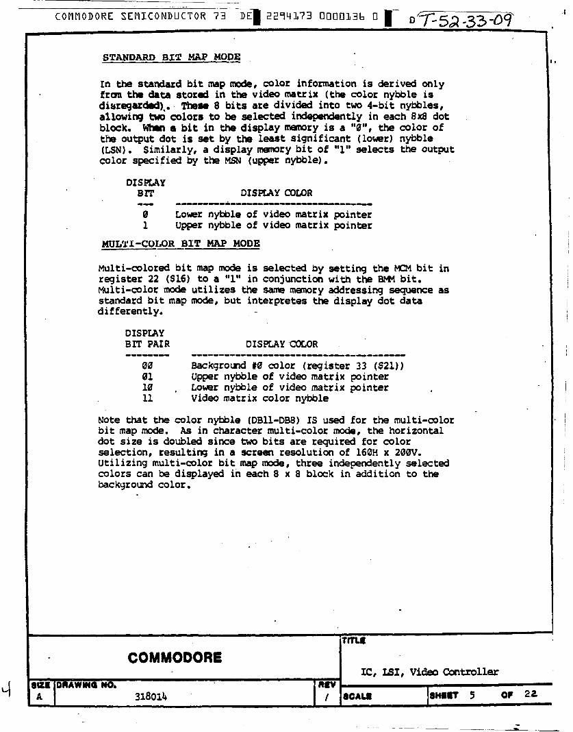
STANDARD BIT MAP MODE
In the standard bit map mode, color information is derived only fran the data stored in the video matrix (the color nybble is disregarded),. These 8 bits are divided into two 4-bit nybbles, allowing two colors to be selected independently in each 8x8 dot block. Whan a bit in the display memory is a "0", the color of the output dot is set by the least significant (lower) nybble (LSN). Similarly, a display memory bit of "1" selects the output color specified by the MSN (upper nybble).
DISPLAYBIT DISPLAY COLOR
0 Lower nybble of video matrix pointer1 Upper nybble of video matrix pointer
MULTI-COLOR BIT MAP MODE
Multi-colored bit map mode is selected by setting the MCM bit in register 22 ($16) to a "1" in conjunction with the B W bit. Multi-color mode utilizes the same memory addressing sequence as standard bit map mode, but interpretes the display dot data differently.
DISPLAYBIT PAIR DISPLAY COLOR
00 Background #0 color (register 33 ($21))01 Upper nybble of video matrix pointer10 Lower nybble of video matrix pointer11 Video matrix color nybble
Note that the color nybble (DB11-DB8) IS used for the multi-color bit map mode. As in character multi-color mode, the horizontal dot size is doubled since two bits are required for color selection, resulting in a screen resolution of 160H x 200V. Utilizing multi-color bit map mode, three independently selected colors can be displayed in each 8 x 8 block in addition to the background color.
• COMMODORETITLI
IC , L S I, Video C o n tro lle rsize
AORAWINa NO*
31801Uftiv
/ 9CALI 8HCKT 5 OP 22.

COMMODORE SEMICONDUCTOR 73 D E | 25^4173 0000137 1
MOVABLE IMAGE BLOCKSThe movable image block (MIB) is a special type of display image which can be displayed at any screen position without the 8x8 dot block constraints inherent in character and bit map modes. Up to 8 unique MIBs can be displayed simultaneously, each defined by 63 bytes in memory displayed as a 24x21 dot array (shown below). A nonber of special features make MIBs especially suited for video graphics and game applicatons.
BYTE BYTE BYTE
00 01 0203 04 05
57 58 5960 61 62
MIB OISPEAY BLOCK
MIB ENABLEEach MIB can be selectively enabled for display by setting its corresponding enable bit (MnE) to "1” in register 21 ($15). If the MnE bit is "0", the MIB will not be displayed.
MIB POSITIONEach MIB is positioned via its X and Y position register (see register map 1.3) within 512 horizontal and 256 vertical positions. The position of a MIB is specified by the upper-left corner of the array. X locations 23 to 347 ($17-5157) and Y locations 50 to 249 ($32-$F9) are visible. Since not all available MIB positions are entirely visible on the screen, MIBs may be moved smoothly on and off the display screen .
TfTL*
COMMODOREIC, LSI, Video Controller
8IZIA
DltAWMa HO*318014
M V/ •CALI SHI IT 6 W 22
COMMODORE SEMICONDUCTOR ~?3 D E j 5214173 DDDD13S 3- r ^ r - 5 ^ - 3 3 ^ 0 9
MIB COLOR
A seperate 4-bit register is associtated with each MIB to specify the MIB color. There ate two MIB colot nodes.
STANDARD MIB COLOR
In the standard mode, a "0" bit of MIB data allows any background, character or bit map data to show through (transparent) and a "1" bit is displayed £s the MIB color determined by the corresponding MIB Color register.
MULTI-COLOR MIB
Each MIB can be individually specified to be multi-color via MnMC bits in the MIB multi-color register 28 ($1C). When the MnMC bit is H1H, the corresponding MIB is displayed in the multi-color mode. In the multi color mode, the MIB data is interpreted in pairs as in the other multi-color modes.
MIBBIT PAIR COLOR DISPLAYED
00 Transparent (background data)01 MIB Multi-color 40 (register 37 ($25))10 MIB Color (registers 39-46 ($27-$2E))11 MIB tolti-color #1 (register 38 ($26))
Since two bits of data are required for each color, the resolution of the MIB is reduced to 12 H x 21 V. Each horizontal dot is expanded to twice the standard size so that the size of the overall MIB does not change. Up to 3 colors can be displayed in each MIB (in addition to transparent), but the two colors specified by the MIB multi-color registers are shared among all 8 MIBs.
MIB MAGNIFICATION
Each MIB can be independently expanded (2X) in both the horizontal and vertical directions. Two registers contain the control bits (MiXE,MnYE) for the magnification control.
RESIGTER ‘ FUNCTION
29 ($1D) Horizontal expand (MiXE) "lH*expand; "0"*normal23 ($17) Vertical expand (MnYE) "1"-expand; "0"-normal
No increase in resolution is realized by expanding the MIBs. The same 24x21 array (or 12x21 if multi-colored) is displayed except but the size of each dot is doubled in the desired direction (up to 4X standard dot dimension if a MIB is both multi-colored andexpanded).
Tims
COMMODOREIC , L S I , Video C o n tro lle r
SIZKA
oRAwma NOk318014
HIV1 •CALI ]8M««T 7 OP 22
COMMODORE SEMI CONDUCTOR 73 D E | 5 5 ^ 1 7 3 □□□0131 5 | ~
MIB PRIO RITY
The priority of each MIB may be individually controlled with respect to the other displayed information (from character or bit map modes).. The priority of each MIB is set by the corresponding bit (MnDP) of register 27 (SIB).
BIT PRIORITY
0 MIB data displayed'instead of any data (in front)1 MIB data displayed only instead of Bkgd #0 or
multi-color bit pair 01 (behind)
MIB data bits of "0" always permit any other information to be displayed (i.e. MIB transparent sections). The MIBs have a fixed priority with respect to each other, with MIB 0 having the highest priority (in front) and MIB 7 the lowest (behind). When MIB data (except transparent data) of two MIBs are co-incident, the data from the lower number MIB will be displayed.
COLLISION DETECTION
Two types of MIB collision (co-incidence) are detected, MIB to MIB collision and MIB to display data collision.
MIB TO MIB COLLISION
A collision between two MIBs occurs when non-transparent output data of two MIBs are co-incident. Co-incidence of MIB transparent areas will not generate a collision. When a collision occurs, the MIB bits (ttiM) in the MIB-MIB COLLISION register 30 ($1E) will be set to "1" for each colliding MIB.The collision bits ranain set until a read of the collision register, when they are automatically cleared. MIBs collisions are detected even if off screen, behind the border.
MIB TO DATA COLLISION
A second register, MIB-DATA COLLISION register 31 ($1F) also contains a bit (MiD) for each MIB which is set to "1" when both the MIB and display data are co-incident. Again, the co-incidence of MIB transparent data and/or display background does not generate a collision. For special applications, the display data from the 0-1 multicolor bit pair also does not cause a collision. This feature permits their use as background display data without interfering with true MIB collisions. A MIB-DATA collision can occur off-screen in the horizontal direction if display data has been scrolled to an off-screen position (see scrolling). The MIB-DATA COLLISION register also automatically clears when read.
COMMODORETITUI
IC , L S I, Video C o n tro lle r
8? 8 DRAWMO NO*318014
RKV/ 9CAIS s h s c t d or 2i
CO MMODORE
MIB COLLISION INTERRUPTS
The collision interrupt latches are set whenever the first bit * of either register is set to "1M. Once any collision bit within a register is set high, subsequent collisions will not set the interrupt latch until that collision register has been cleared to all "CTs by a read.
MIB MEMORY ACCESS
The data for each MIB is stored in 63 consecutive bytes of memory. Each block of MIB data is defined by a MIB pointer, located at the end of the VIDEO MATRIX. Since only 1,000 bytes of the video matrix are used in the normal display modes video matrix locations 1016-1023 ($3F8-$3FF) are used for MIB pointers 0-7 respectively. The eight bit MIB pointer from the video matrix together with the six bits from the MIB byte counter to count through the 63 bytes define the entire 14-bit address field.
A13 A12 All A10 A09 A08 A07 A06 A05 A04 A03 A02 A01 A00
MP7 MP6 MP5 MP4 MP3 MP2 MPl MP0 MC5 MC4 MC3 MC2 MCI MC0
The MPx are the MIB pointer bits from the video matrix and MCx are the internally generated MIB counter bits. The MIB pointers are read from the video matrix at the end of every raster line. When the Y position register of a MIB matches the current raster line count, the actual fetches of MIB data begin. Internal counters automatically step through the 63 bytes of MIB data, displaying three bytes on each raster line.
OTHER FEATURES
SCREEN BLANKING
The display screen may be blanked by setting the BLNK bit in register 17 ($11) to a H1H. when the screen in blanked, the entire screen displays the exterior color specified by register 32 ($20). When blanking is enabled, only transparent (Phase 1) memory accesses are required, permitting full processor utilization of the system bus. However, MOB data will be accessed if the MOBS are not also disabled.
MIB DATA ADPRESS
TITLt
COMMODOREIC, LSI, Video Controller
• fz i jDftAwm a no*A 3 1 8 0 1 U
ftffV — / SCA kl SHICT 9 OF 2 2
COMMODORE SEMICONDU CTOR 73 » E | 5ET4173 OOOQ141 3’J ~
DISPLAY ROW/COLUMN SELECT
The normal display space consists of 25 cows of 40 character regions per row. For special display purposes, the display window may be reduced to 24 rows or 38 characters. There is no change in the format of the displayed information, except that characters (bits) adjacent to the exterior border area are covered by the border. -
RSEL Number of rows CSEL Niihber of colunns
0 24 rows 0 38 colunns1 25 rows 1 40 columns
The RSEL bit is in register 17 ($11) and the CSEL bit is inregister 22 ($16). For standard display the larger display window is normally used, while the smaller display window is normally used in conjunction with scrolling.
SCROLLING
The display data may be scrolled up to one character region in both the horizontal and vertical direction. When used in conjixiction with the smaller display window (above), scrolling can be used to create a smooth panning motion of display data while updating the system memory only when a new character row (or column) is required. Scrolling is also used for centering a display within the screen.
BITS . REGISTER FUNCTION
X2,XI,X0 -22 ($16) Horizontal positionY2,Y1,Y0 17 ($11) vertical position
LIGHT PEN
The light pen input latches the current screen position into a pair of registers.(LPX,LPY) on a low-going edge. The X position register 19 ($13) contains the 8 MSB of the X position at the time of transition. Since the X position is defined by a 9 bit coulter, resolution to 2 horizontal dots is provided. Similarly, the Y position is latched in its register 20 ($14) with 8 bitsprovide unique raster resolution within the visible display. The light pen latch may be triggered only once per frame, and subsequent triggers within the same frame will have no effect.
C O M M O D O R E
TiTLC
IC , L S I, Video C o n tro lle r
8121A
DRAWING NO.318014
R*V/ SCALS 8H8CT 10 OF 2 2
• ------ -■ ..............— .................... . - ...............
COMMODORE SEMICONDU CTOR 73 D E j 22=54173 D O Q D m a SI y T - 5 3 - 3 3 - 0 ?
RASTER REGISTER
The raster register is a dual function register. A read of the raster register 18 ($12) returns the lower 3 bits of the current raster positon (the MSB-RC8 is located in register 17 ($11)). Awrite to the raster bits (including RC8) is latched for use in an internal raster compare. When the current raster matches the written value, the raster interrupt latch is set. The raster register should be interrogated to prevent display flicker by delaying display changes to occur outside the visible area. The visible area of the display is from raster 51 to raster 251 ($033-$0FB).
INTERRUPT REGISTER
The interrupt register indicates the status of the four sources of interrupt. An interrupt latch in register 25 ($19) is set to "I" when an interrupt source has generated an interrupt request.
WHEN SET
Actual raster comt » stored raster count MOB-DATA collision (first bit only) MOB-MOB collision (first bit only)First negative transition of LP per frame When IRQ/ output low
LATCH ENABLEBIT BIT
TRST ERSTIMDC EMDCIftC EMMCILP . ELPIRQ
•'0", theTo enable an interrupt request to set the IRQ/ output to corresponding interrupt enable bit in register 26 ($1A) must beset to "I”. Once an interrupt latch has been set, the latch may be cleared only by writing a "1" to the associated bit in theinterrupt register. This feature allows selective handling ofvideo interrupts without software storing of the activeinterrupts.
DYNAMIC RAM REFRESH
A dynamic ram refresh controller is built in to the 6567 device. Five 8-bit row addresses are refreshed every raster line. Thisrate guarantees a maximum delay of 2.02 ms between the refresh of any single row address in a 128 refresh scheme. (The maximum delay is 3.66ms in a 256 address refresh scheme). This refresh is totally transparent to the system, since the refresh occurs during Phase 1 of the system clock. The 6567 generates both SAS/ and CAS/ which are normally connected directly to the dynamic rams. RAS/ and CAS/ are generated for every Phase 2 and every video data access (including refresh) so that external clock generation is not required.
COMMODORETim
IC , 1 5 1 , Video C o n tro lle r8B I lOAAWIMO NOkA 1 318014
RKV/ 8CAL8 |SHf«T n 0* 22
COMMODORE SEMICONDUCTO R 73 D E | 5214173 DDOD143 7 1 ~ T ^ 5 ^ T 3 3 ^ 0 ^
COLOR CODE TABLE
OB11 OB10 DB09 DB08 HEX COLOR
0 0 . 0 0 $0 Black. 0 0 0 I $1 White0 ■ 0 • 1 0 $2 Red0 0 1 1 $3 Cyan0 •v -A ■. 0 0 $4 Purple0 ,1 ' 0 1 $5 Green0 l 1 0 56 - Blue0 l 1 1 S7 Yellow1 0 0 0 $8 Orange1 0 0 1 $9 Brown1 0 1 0 $A Light Red1 0 1 1 SB Dark Grey1 l 0 0 $C Medium Grey1 l 0 1 $D Light Green1 l 1 0 $E Light Blue1 l 1 1 $F Light Grey
COMMODORE
[SBCA
CHAWING HOk313014
m v/
TITLI
IC, LSI, Video Controller
SCALI SH **T 1 2 OP 2 2
COMMODORE SEMICONDUCTOR 73 D E | 5214173 0D00144 1 ^ y <f ^ 5 ^ 3 3 ^ 0 ^
*
SCREEN POSITION DECODES
HORIZONTAL DECODES
NAME SET CLEAR FUNCTION
HSYNC 416 452 Horizontal sync pulseHEQl 178 196 Horizontal equalization pulse 1HEQ2 434 452 Horizontal equalization pulse 2HBLANK 396 496 Blanks video during horiz retraceBURST 456 492 Gates reference color burstBKDE38 35 339 Enables 38 column backgroundBKDE40 28 348 Enables 40 colunn backgroundBOL 508 4 Begin line (internal clock)EOL 340 346 End line (internal clock)VINC 404 412 Increment vertical counterCW 12 332 Enable character £etchVMBA 496 332 Buss avail for character fetchREFW 484 12 Enable dynamic ram refreshSPBA 336 376 3uss avail for sprite #0 fetch
VERTICAL DECODES
NAME SET CLEAR FUNCTION
VRESET 261 n/a Resets vertical count to zeroVSYNC 17 20 Enables vertical syncVEQ 14 , 23 Enables vertical equalazationVBLANK 13 24 Blanks video during vert retraceVSW24 55 247 Enables 24 row screen windowVSW24 51 251 Enables 25 row screen windowEEVMF 48 248 Enables character fetch
COMMODORE
801
A
DRAWING NOk
31801U
RtV/
T IT LI
IC . L S I, Video C o n tro lle r
8GALI S H U T 1 3 OF 2 2
CO MM OD ORE SEM IC ON DU C TO R 73 D E | EET4173 0000145 0 | o 3 3 -O *?
REGISTER MAPADORESS DB7 DB6 DBS DB4 DB3 DB2 DB1 DB0 DESCRIPTION
00($00) M0X7 M0X6 M0XS M0X4 M0X3 M0X2 M0X1 M0X0 MIB 0 X-position01($01) M0Y7 M0Y6 M0Y5 M0Y4 M0Y3 M0Y2 M0Y1 M0Y0 MIB 0 Y-position02($02) M1X7 M1X6 M1X5 M1X4 M1X3 M1X2 M1X1 M1X0 MIB 1 X-position03($03) M1Y7 M1Y6 M1Y5 M1Y4 M1Y3 M1Y2 MlYl M1Y0 MIB 1 Y-position04($04) M2X7 M2X6 M2X5 M2X4 M2X3 M2X2 M2X1 M2X0 MIB 2 X-position05($05) M2Y7 M2Y6 M2Y5 M2Y4 M2Y3 M2Y2 M2Y1 M2Y0 MIB 2 Y-position06($06) M3X7 M3X6 M3X5 M3X4 M3X3 M3X2 M3X1 M3X0 MIB 3 X-position07($07) M3Y7 M3Y6 M3Y5 M3Y4 M3Y3 M3Y2 M3Y1 M3Y0 MIB 3 Y-position08($08) M4X7 M4X6 M4X5 M4X4 M4X3 M4X2 M4X1 M4X0 MIB 4 X-position09($09) M4Y7 M4Y6 M4Y5 M4Y4 M4Y3 M4Y2 M4Y1 M4Y0 MIB 4 Y-position10 ($0A) M5X7 M5X6 M5X5 M5X4 M5X3 M5X2 M5X1 M5X0 MIB 5 X-position11 ($0B) M5Y7 M5Y6‘M5Y5 M5Y4 M5Y3 M5Y2 M5Y1 M5Y0 MIB 5 Y-position12($0C) M6X7 M6X6 M6X5 M6X4 M6X3 M6X2 M6X1 M6X0 MIB 6 X-position13($0D) M6Y7 M6Y6 M6Y5 M6Y4 M6Y3 M6Y2 M6Y1 M6Y0 MIB 6 Y-position14($0C) M7X7 M7X6 M7X5 M7X4 M7X3 M7X2 M7X1 M7X0 MIB 7 X-position15($0F) M7Y7 M7Y6 M7Y5 M7Y4 M7Y3 M7Y2 M7Y1 M7Y0 MIB 7 Y-position16 ($10) M7X8 M6X8 M5X8 M4X8 M3X8 M2X8 M1X8 M0X8 MSB of X-position17($11) RC8 ECM Bl*! BLNK RSEL Y2 Y1 Y0 See text18($12) HC7 RC6 RC5 RC4 RC3 RC2 RC1 RC0 Raster register19($13) LPX8 LPX7 LPX6 LPX5 LPX4 LPX3 LPX2 LPXl Light Pen X20($14) LPY7 LPY6 LPY5 LPY4 LPY3 LPY2 LPYl LPY0 Light Pen Y21($15) M7E M6E M5E M4E M3E M2E M1E M0E MIB Enable22($16) - - RES MZM CSEL X2 XI X0 See text23($17) M7YE M6YE M5YE M4YE M3YE M2YE Ml YE M0YE MIB Y-expand24($18) VM13 VM12 VM11 VM10 CB13 CB12 CB11 - Memory Pointers25($19) IRQ/ - - - ILP i m c IMBC IRST Interrupt Register26($1A) - - - - ELP EMC EMBC ERST Enable Interrupt27($1B) M70P M6DP M5DP M4DP M3DP M2 DP MIDP M0DP MIB-DATA Priority28($1C) M7MC M6MC M5MC M4MC M3MC M2MC M1MC M0MC MIB Multicolor Sel29($10) M7XE M6XE M5XE M4XE M3XE M2XE M1XE M0XE MIB X-expand30($1E) M7M M6M M5M M4M M3M M2M M1M M0M MIB-MIB Collision31($1F) M7D M6D M5D M4D M3D M2D MID M0D MIB-DATA Collision32($20) - - - - EC3 EC2 SCI BC0 Exterior Color33($21) - - - - B0C3 B0C2 B0C1 B0C0 Bkgd #0 Color34($22) - - - - B1C3 B1C2 B1C1 B1C0 Bkgd #1 Color35($23) - - - - B2C3 B2C2 B2C1 B2C0 Bkgd #2 Color36($24) - - - - B3C3 B3C2 B3C1 B3C0 Bkgd #3 Color37($25) - - - - MM03 m$2 f«01 M M MIB Multicolor #038($26) - - - • f*ll3 f*112 rtm NM10 MIB Multicolor #139($27) - - - - M0C3 M0C2 M0C1 M0C0 MIB 0 Color40($28) - - - - M1C3 M1C2 M1C1 M1C0 MIB 1 Color41($29) - - - - M2C3 M2C2 M2C1 M2C0 MIB 2 Color42($2A) - - - - M3C3 M3C2 M3C1 M3C0 MIB 3 Color43($2B) - - - - M4C3 M4C2 M4C1 M4C0 MIB 4 Color44 ($2C) - - - - M5C3 M5C2 M5C1 M5C0 MIB 5 Color45($2D) - - - - M6C3 M6C2 M6C1 M6C0 MIB 6 Color46($2E) - - - M7C3 M7C2 M7C1 M7C0 MIB 7 Color
MOTE: All dashes read as "lN regardless of written value.
TITLf
COMMODORE IC, LSI, Video Controller
801A
DRAWNM HO.318014
ft IV1 8CAV1 8H88T 14 OP 22
COMMODORE
SYSTEM INTFERACE
The 6567vidso controller device interacts with the system data bus in a unique way. a 65XX system requires the system busses only during the Ptiase 2 (clock high) portion of the cycle. The 6567 device takes advantage of this characteristic by normally accessing system memory only during the Phase 1 (clock low) portion of the clock cycle. Therefore, operations such as character data fetches and memory refresh are totally transparent to the processor and do not reduce the processor through-put. The video chip provides the interface control signals required to maintain this bus sharing.
AEC PH0 CS/ R/W ACTION
0 0 X X PHASE 1 - 8562 MEMORY FETCH0 1 X X PHASE 2 - DMA (PROCESSOR OFF)1 1 0 0 WRITE TO 8562 REGISTER1 1 0 I READ FROM 8562 REGISTER1 1 1 X PROCESSOR MEMORY CYCLE
BUSS MUTLIPLEXING
The video circuit provides the AEC signal (address enable control) which is used to disable the processor address bus drivers, thereby allowing the video device to access the address bus. AEC is active low which permits direct connection to the AEC input of the 65XX family. The AEC signal is activated during every Phase 1 so that processor operation is not normally affected. Because of this bus "sharing", all memory accesses must be completed in 1/2 cycle. Since the video chip provides a IMhz clock (which should be used as system phase 2), a memory cycle is 500ns including address setup, data access and data setup to the reading device.
DMA OPERATION
Certain operations of the 6567require data at a faster rate than available by reading only during the Phase 1 time; specifically, the access of character pointers from the video matrix and the fetch of MIB data. Therefore, the processor must be disabled and the data accessed during the Phase 2 clock. This is accomplished via the BA (bus available) signal. The BA line is normally high but is brought low during Phase 1 to indicate that the video chip will require a Phase 2 data access. Three Phase 2 times are allowed after BA low for the processor to complete any current memory accesses. On the fourth Phase 2 after BA low, the AEC signal will remain low during Phase 2 as the video chip fetches data. The BA line is normally connected to the RDY input of a 65XX processor. The character pointer fetches occur every eighth raster line during the display window and require 40 consecutive Phase 2 accesses to fetch the video matrix pointers.
TiTte
COMMODORE IC, LSI, Video Controller
JiAwma n o . fl|V II-!1 SCALf318014 3HIIT 15 OF 22
COMMODORE S EMICONM JCTOR^73 D E | 2514173 0000147 4
The MIB pointers are fetched every other Phase 1 at the end of each raster line. As needed, additional cycles are used for MIB data fetches, with all necessary bus control provided by the 8562 device.
INTEFSCE SIGNAL DESCRIPTION
2.8.3.1 DATA BUS (DB7-DB0)
The eight data bus pins are the bi-directional data port, controlled by CS/, RW, and Phase 0. The data bus can only be accessed while AEC and Phase 0 are high and CS/ is low.
CHIP SELECT (CS/1)
The chip select pin, CS/, is brought low to enable access to the circuit registers in conjunction with the address and RW pins. CS/ low is recoginzed only while AEC and Phase 0 are high.
READ/WRITE (R/W)
The read/write input, R/W, is used to determine the direction of data transfer on the data bus, in conjunction with CS/. When R/W is high .("1") data is transfered from the selected register to the data bus output. When RAtf is low (*'0") data presented on the data bus pins is loaded into the selected register.
ADDRESS BPS (A1O-A0)
Address pins A06-A00 are multiplexed to allow direct connection to dynamic RAMs. During the row address time, A06-A00 are driven on pins A06-A00, while A13-A08 are driven on pins A05-A00
for the entire memory cycle. The lower six address pins, A05-A00, are also bi-directional. During a processor read or write of the video device, address pins A35-A00 are inputs which latch on the low edge of RAS/. The data on these address inputs selects the register for read or write as defined in the register map.
CLOCK OUT
The clock output, Phase 0, is the IMhz clock used as the 65XX processor Phase 0 in. All system bus activity is referenced to this clock. The clock frequency is generated by dividing the 8Mhz video input clock by eight. ___________________
PHASE DATA CONDITION
1212
MIB Pointer Every rasterMIB Byte 1 Each raster while MIB is displayedMIB Byte 2 Each raster while MIB is displayedMIB Byte 3 Each raster while MIB is displayed
and pin A06 is "I" during the column time. A10-A07 is stable
TITL*
COMMODORE IC, LSI, Video Controller
StZI jDrtAWMd NOtA 318014
M V — / 8CAL1 shut 16 or 2.2
COMMODORE S E M I C O N D U C T O R ~ 73 F eJ 2514173 0000143 b
RAS/CAS
The RAS/ and CAS/ signals provide the timing signals necessary for dynamic RAMs. These signals are provided twice each clock out cycle.to support a memory cycle during both phase 1 and phase 2.
INTERRUPTS (IRQ/)
The interrupt output, IRQ/, is brought low when an enabled source of interrupt occurs with in the device. The IRQ/ output is open drain, requiring an external pull-ig> resistor.
VIEDO INTERFACE
The video output frcro the 6567 consists of two signals which must be externally mixed together to create NTSC compatible composite video. After appropriate mixing, the resulting signal can directly drive a video monitor or RF modulator for use with a standard television.
VIDEO CLOCK IN
This clock input is the fundamental dot shift rate clock. In addition, all other video sync and system interface signals are derived by dividing this clock. Normally, the desired frequency is 9 Mhz. The primary constaints are the system timing and the requirement that one horizontal raster line is 520 video clock cycles.
COLOR CLOCK IN
The color clock is used to derive the chrananince signal. NTSC video systems require this input to be 14.31818 Mhz. This base frequency is divided by 4 internally and then appropriately phase shifted to create the 3.5795 Mhz video color signal for NTT SC applications.
SYNC/LUM OUTPUT
SYNC/LUM output from the 6567 contains all the video data, including horizontal and vertical syncs, as well as the luninancJe information of the video display is an open drain output requiring an external pullup of 500 ohms.
COLOR OUTPUT
The COLOR output contains all the chrominance information, including the color reference burst and the color of all display data. The COLOR output is open source and should be terminated with 1,000 ohms to ground.
TITLI
COMMODOREIC, LSI, Video Controller
StZI IDRAWIMQ NO* ftSV ...■—1 9CALSA 318014 8 HC8 T 17 OP 22
COMMODORE SEMICONDUCTOR 73 DE| 22^4173 0DD014T fl | ~ ^ T ^ S Q ^ 3 ^ 7 o ^
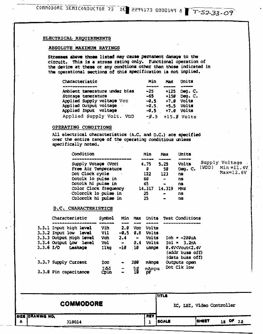
ELECTRICAL REQUIREMENTS
ABSOLUTE MAXIMUM RATINGS
Stresses above those listed may cause permanent damage to the circuit. This is a stress rating only. Functional operation of the device at these or any condtions other than those indicated in the operational sections of this specification is not implied.
Characteristic Min Max Units
Ambient temerature under bias -25 +125 Deg. C.Storage temerature -65 +150 Deg. C.Applied Supply voltage Vcc -0.5 +7.0 VoltsApplied Output voltage -0.5. +5.5 VoltsApplied Input voltage -0.5 +7.0 voltsApplied Supply Volt. VDD ~0 • 5 +15.0 Volts
OPERATING CONDITIONS
All electrical characteristics (A.C. and D.C.) are specifiedover the entire range of the operating conditious 'unlessspecifically noted.
Condition Min Max units
Supply Votage (Vcc) 4.75 5.25 Volts SupplyFree Air Temperature 0 50 Deg. C.Dot Clock cycle 122 123 nsDotclk lo pulse in 60 - nsDotolk hi pulse in 45 - nsColor Clock frequency 14.317 14.319 MHZColorclk lo pulse in 25 - nsColorclk hi pulse in 25 - ns
Min -II. 4V Max-12.6V
D.C. CHARACTERISTICS
Characteristic Symbol Min Max Units Test Conditions— — — — —
3.3.1 Input high level Vih 2.0 VCC Volts3.3.2 Input low level Vil -0.5 0.8 VOltS3.3.3 Output High level Voh 2.4 - VOltS Ioh * -200uA3.3.4 Output &ow level Vol - 0.4 volts Iol 3 3.2mA3.3.6 I/O Leakage 11kg -10 .10 uAmps 0.4V<Vout<2.4V
3.3.7 Supply Current Icc 200 mAmps
(addr buss off) (data buss off) Outputs open
3.3.8 Pin capacitanceIddCpin
5010
mAmpspF
Dot Clk low
COMMODORE
SIZIA
ORAWMQ NOk318014
M V1
T1T L *
IC, LSI, Video Controller
8CALI S H U T is OP 2 2
COMMODORE SEMICONDU CTOR 73 D E I 22T4173 DDDDISD 4 ^
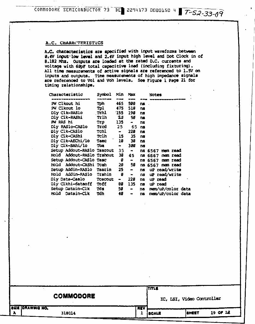
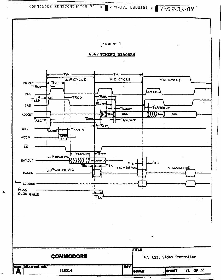
A.C. CHARACTERISTICS
A.C. characteristic* are specified with input waveforms between 0i4V input'low level and 2.4V input high level and Dot Clock in of 8.182 Mhz. Outputs are loaded at the rated D.C. currents and voltage with 60fcF total capacitive load (including fixturing).All time measurements of active signals are referenced to 1.5V on inputs and outputs. Time measurements of high impedance signals are referenced to Vol and Voh levels. See Figure 1 Page 21 for timing relationships.
Characteristic Symbol Min Max Notes
PW Clkout hi Tph 465 500 nsPW clkout lo Tpl 475 510 nsDly Clk-RASlo Trhl 155 190 nsDly Clk-RAShi Trlh £3 50 nsPW RAS hi Trp 135 - nsDly RASlo-CASlo Trcd 25 65 nsDly Clk-CASlo Tchl - 220 nsDly Clk-CAShi Tclh 15 35 nsDly Clk-AEChi/lo Taec 10 30 nsDly Clk-BAhi/lo Tba - 300 nsSetup Addout-RASlo Tasrout 35 - ns 6567 man readHold Addout-RASlo Trahout 30 45 ns 6667 mem readSetup Addout-CASlo Tasc 0 - ns 6567 mem readHold Addout-CAShi Tcah 20 50 ns 6567 mem readSetup Addin-RASlo Tasrin 25 - ns uP read/writeHold Addin-RASlo Trahin 0 - ns uP read/writeDly Data-Caslo Tcacout - 220 ns up readDly Clkhi-dataoff Toff 80 135 ns up readSetup Oatain-Clk lids 50 - ns menv/uP/color dataHold Datain-Clk Tdh 40 - ns mem/uP/color data
COMMODORE
SK IA
QRAWMO NO.318014
RKV1
TITLIIC, 151, Video Controller
8CALI SHIKT 19 OP 2£
COMMODORE SE MICONDUCTOR "73 D E | 2514173 DDOD1S1 ^ - 3 3 ' Q ?
FIGURE 1
6 5 6 7 TIMING DIAGRAM
TfTLI
COMMODORE IC , L S I, Video C o n tro lle r
a ^ l JDfMWMHI MO»318014
ravM ALI |«MOT 21 0 ^ 22


![4173 7Y07 IELTShbk_body [prf5]](https://static.fdocuments.in/doc/165x107/586cc1fd1a28ab55088bdd04/4173-7y07-ieltshbkbody-prf5.jpg)