Commercializing TSV 3DIC Wafer Process Technology...
18
1 2013 SEMICON China 3D-IC Forum Commercializing TSV 3DIC Wafer Process Technology Solutions for Next Generation of Mobile Electronic Systems Dr. Shiuh-Wuu Lee, Sr. VP of Technology Research & Development Semiconductor Manufacturing International Corporation March 20, 2013
Transcript of Commercializing TSV 3DIC Wafer Process Technology...

1
2013 SEMICON China 3D-IC Forum
Commercializing TSV 3DIC Wafer Process
Technology Solutions
for Next Generation of Mobile Electronic Systems
Dr. Shiuh-Wuu Lee, Sr. VP of Technology Research & Development
Semiconductor Manufacturing International Corporation
March 20, 2013
Safe Harbour Statement
Standard Disclaimer

Safe Harbour Statement

Safe Harbour Statement

5
� Driving Forces for 3DIC at System & Device Levels
� TSV-based 3DIC SiP for Handheld to Wearable
� Technology Readiness across Supply-Chain
� Outweighing Controlling Factors in Solutions & Evolution
� Collaborative Supply-Chain 3DIC Foundry Model
� Closing Remarks
Outline
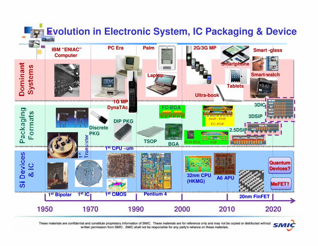
Evolution in Electronic System, IC Packaging & Device
202020102000199019701950
IBM IBM ““ENIACENIAC””
Computer Computer
11stst ICIC11stst BipolarBipolar
11stst CPU ~umCPU ~um
DiscreteDiscrete
PKGPKG
DIP PKGDIP PKG
TSOPTSOPBGABGA
FCFC--BGABGA
Pentium 4Pentium 4
32nm CPU32nm CPU
(HKMG)(HKMG)A6 APUA6 APU
20nm FinFET20nm FinFET11stst CMOSCMOS
PC EraPC Era
LaptopLaptop
PalmPalm
1G MP1G MP
DynaTAcDynaTAc
2G/3G MP2G/3G MP
UltraUltra--bookbook
TabletsTablets
SmartphoneSmartphone
SmartSmart--watchwatch
Smart Smart --glassglass
QuantumDevices?
QuantumQuantum
Devices?Devices?
2.5DSiP2.5DSiP
3DSiP3DSiP
3DIC3DIC
MeFET????MeFETMeFET????????
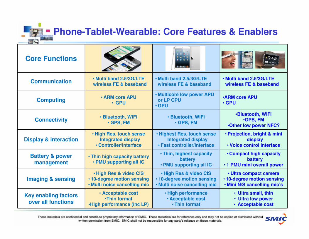
Phone-Tablet-Wearable: Core Features & Enablers
Core Functions
Communication• Multi band 2.5/3G/LTE wireless FE & baseband
• Multi band 2.5/3G/LTE wireless FE & baseband
• Multi band 2.5/3G/LTE wireless FE & baseband
Computing• ARM core APU
• GPU
• Multicore low power APU or LP CPU
• GPU
•ARM core APU• GPU
Connectivity• Bluetooth, WiFi
• GPS, FM• Bluetooth, WiFi
• GPS, FM
•Bluetooth, WiFi•GPS, FM
•Other low power NFC?
Display & interaction• High Res, touch sense
Integrated display• Controller/interface
• Highest Res, touch sense Integrated display
• Fast controller/interface
• Projection, bright & mini display
• Voice control interface
Battery & power management
• Thin high capacity battery• PMU supporting all IC
• Thin, highest capacity battery
• PMU supporting all IC
• Compact high capacity battery
• 1 PMU mini overall power
Imaging & sensing• High Res & video CIS
• 10-degree motion sensing• Multi noise cancelling mic
• High Res & video CIS• 10-degree motion sensing• Multi noise cancelling mic
• Ultra compact camera• 10-degree motion sensing• Mini N/S cancelling mic’s
Key enabling factorsover all functions
• Acceptable cost•Thin format
•High performance (inc LP)
• High performance• Acceptable cost
• Thin format
• Ultra small, thin• Ultra low power• Acceptable cost

Evolution of IC & Electronic System Integration
Now FurtherRelated Technology Enhancements
TSV 3DIC:Pro & Con
Dominant Driving of Systems
SmartphoneTablet
e-Wearable's:Smart-watchSmart-glass
• Thinner, lighter, smaller• Low power, high speed• Connectivity, computing,
interactivity• Flat or lower costs
•++•++
• --
Trend: IC & SubsystemPackaging
PoP, MCM, Discrete onPCB
More “3D”SiP on PCB, less discrete & isolated MCM
•Higher, denser I/O pins•More RDL layers in SiP•Thinner, smaller format•Hybrid stack integration•Lower cost,•Better reliability
•++•++•++•++• --•+
IC Devices & Fabrication
HKMG to FinFET
FinFETbulk Si,SOI
•Better device variation management
•Decouple logic with MS/RF to 2 chips, maybe at different nodes or technologies
•++
•++

Front Side MCP/SiP TSV SiP Opt Back Side MCP/SiP TSV Opt
WiFi module WiFi Combo
wireless processor
WFi FE
May use TSV SiP
but costly
APU DRAM MCP TSV Wide I/O best
option but costly &
manufacturability
3-axis gyro MEMS+ASIC SiP TSV SiP: thinner,
better noise isolation
Combo SiP:
Single chip
LTE Baseband Processor
PMIC on front-side
connected through PCB
Split logic potion
with MS/RF to two chips, 2.5D SiP
3-axis accelerometer
MEMS+ASIC SiP Audio Chips 1/2 Chip MCP May stay separated for noise isolation
Touch screen controller
BCM interface Performance gain but costly
Imaging Sensor Camera Module
8 or 13M BSI Can further thinner WL camera module
GSM/GPRS/EDGEPA
SiP with matching
switches, IPD, LNA
TSV SiP for PA
module: improving noise performance,
but cost needs
justification
Microphones 3 in different
packages & sites
No help
CDMA PA
GSM PA
LTE PA
Multiband FE
WCDMA PA
Example: Chips to SiP Grouping on Smartphone PCB
Front-side
Back-side

Device Level: Alternative “Process Integration”
Core LogicCore Logic MemoryMemory SpecialtySpecialty
Core LogicCore Logic
MemoryMemory SpecialtySpecialty
2 Poly Cell2 Poly CellFine pitch stacked arrayFine pitch stacked array
Special implants & thermal budgetSpecial implants & thermal budget
Specialty MOSSpecialty MOS
Large CD range & patternsLarge CD range & patternsSpecial implants & analog Special implants & analog
performanceperformance
HS/LP dominant (to FinFET)HS/LP dominant (to FinFET)Ultra fine CD, fine arrayUltra fine CD, fine array
Baseline implants & constrained Baseline implants & constrained thermal budgetthermal budget
Enhanced, dedicated CMOS (FinFET) designEnhanced, dedicated CMOS (FinFET) design
Better ultra fine CD & OPC controlBetter ultra fine CD & OPC control
Simplified baseline implants & thermal budgetSimplified baseline implants & thermal budget
Dedicated memory MOSDedicated memory MOS
Better fine pitch dense Better fine pitch dense
array & OPCarray & OPC
Optimized implants & Optimized implants &
thermal budgetthermal budget
Dedicated specialty MOSDedicated specialty MOS
Gross litho CD & variable Gross litho CD & variable
patternspatterns
Specialized implants & Specialized implants &
analog tuninganalog tuning

Chip Level: Alternative “Interconnect” to 2D SOC
2D homogenous SOC
1. FEOL CD => ~10nm, BEOL CD ~10’s nm; narrowing long on-chip interconnects
2. IMD advance (LK => ELK) cease & limit further RC reduction
Logic layerLogic layer
TSV layerTSV layer
Memory layerMemory layer
3D reconfigured architecture
TSV 3DTSV 3D
Die sizeDie size
MT XMT X--secsec
MT lengthMT length
RC delayRC delay
PowerPower
2D SOC2D SOC
Die sizeDie size
MT XMT X--secsec
MT lengthMT length
RC delayRC delay
PowerPower
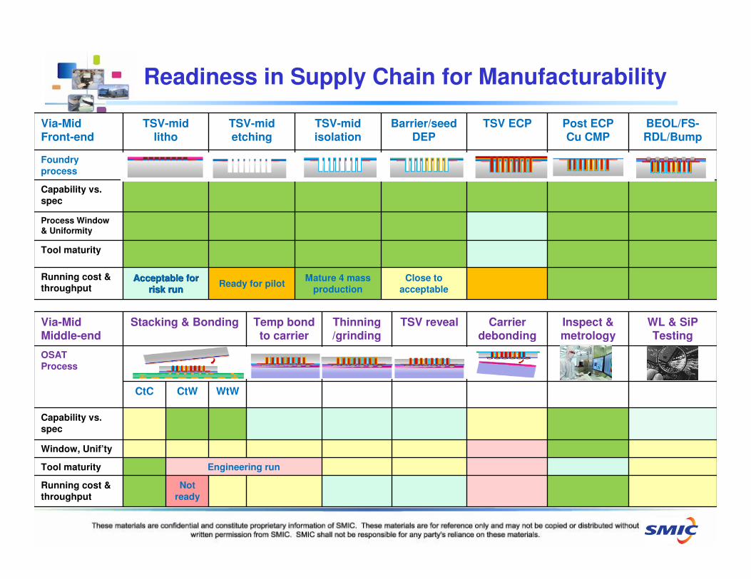
Via-Mid Front-end
TSV-mid litho
TSV-mid etching
TSV-mid isolation
Barrier/seedDEP
TSV ECP Post ECP Cu CMP
BEOL/FS-RDL/Bump
Foundry process
Capability vs. spec
Process Window & Uniformity
Tool maturity
Running cost & throughput
Acceptable for Acceptable for
risk runrisk runReady for pilot
Mature 4 mass production
Close to acceptable
Readiness in Supply Chain for Manufacturability
Via-Mid Middle-end
Stacking & Bonding Temp bond to carrier
Thinning /grinding
TSV reveal Carrier debonding
Inspect & metrology
WL & SiP Testing
OSATProcess
CtC CtW WtW
Capability vs. spec
Window, Unif’ty
Tool maturity Engineering run
Running cost & throughput
Not ready
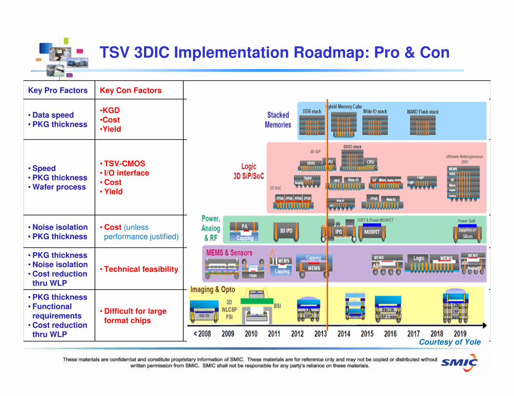
Key Pro Factors Key Con Factors
• Data speed• PKG thickness
•KGD•Cost•Yield
• Speed• PKG thickness• Wafer process
• TSV-CMOS• I/O interface• Cost• Yield
• Noise isolation• PKG thickness
• Cost (unless
performance justified)
• PKG thickness• Noise isolation• Cost reduction
thru WLP
• Technical feasibility
• PKG thickness• Functional
requirements• Cost reduction
thru WLP
• Difficult for large format chips
TSV 3DIC Implementation Roadmap: Pro & Con
Courtesy of Yole
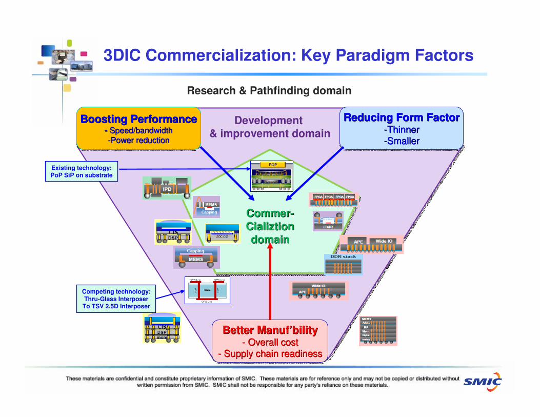
3DIC Commercialization: Key Paradigm Factors
Boosting Performance- Speed/bandwidth
-Power reduction
Boosting PerformanceBoosting Performance-- Speed/bandwidthSpeed/bandwidth
--Power reductionPower reduction
Reducing Form Factor-Thinner-Smaller
Reducing Form FactorReducing Form Factor--ThinnerThinner
--SmallerSmaller
Better Manuf’bility- Overall cost
- Supply chain readiness
Better ManufBetter Manuf’’bilitybility-- Overall costOverall cost
-- Supply chain readinessSupply chain readiness
Commer-Cializtiondomain
CommerCommer--
CializtionCializtion
domaindomain
Research & Pathfinding domain
Development & improvement domain
Competing technology:Thru-Glass Interposer
To TSV 2.5D Interposer
Existing technology:PoP SiP on substrate

Emerging Mid-End & Two Ecosystem Models
Courtesy of Yole
•• Technical spec (DR, etc) & handTechnical spec (DR, etc) & hand--off: must shared from FE, ME, BE to systemoff: must shared from FE, ME, BE to system
•• Productization & commercialization only verified along full liProductization & commercialization only verified along full line down to system levelne down to system level•• Foundry & OSAT best to leverage existing differentiating but maFoundry & OSAT best to leverage existing differentiating but matching core strength tching core strength
& capability over ME, extended from FE and BE respectively& capability over ME, extended from FE and BE respectively

Collaborative Full 3DIC Foundry Services
Key Key
Competency Competency
& Services& ServicesIC DesignIC Design
Devices on Devices on
Wafer Fab & Wafer Fab &
WL TestingWL Testing
Wafer Wafer
Level Level
PackagingPackaging
Chip to System Chip to System
Packaging Packaging
&Testing&Testing
System & System &
Board Board
AssemblyAssembly
(Sub) System (Sub) System
Design & Design &
ApplicationApplication
IDMIDM’’ss
Or waferOr wafer+WLP+P&T+WLP+P&T
FabFab--lite & lite & fablessfabless
CMOS Wafer CMOS Wafer
FoundryFoundry
WLP PartnerWLP Partner
Chip & SiP & Chip & SiP &
Testing Testing PartnerPartner
System System
Assembler & Assembler & UserUser
Core Value& Strength
Core ValueCore Value
& Strength& StrengthDesignService
TSVVia-mid
Complete vertical integrationComplete vertical integrationComplete vertical integration
Collaborative 3DICCollaborative 3DIC
Foundry ModelFoundry Model
Core Value& Strength
Core ValueCore Value
& Strength& Strength
ExtService
Expandedservice
Core Value & Strength
Core Value Core Value
& Strength& Strength
ExtServ
Core Value& Strength
Core ValueCore Value
& Strength& Strength
Core Value& Strength
Core ValueCore Value
& Strength& StrengthExtService
Full foundry modelFull foundry modelFull foundry model
•• Extra Capex $Extra Capex $
•• New,diff OPSNew,diff OPS
•• Limited capacityLimited capacity
•• High MFG $High MFG $
Closing Remarks
Systems towards mobile wearable fundament to driving supply chain to TSV 3DIC development & commercialization
• Mobile, handheld to wearable inevitable, the dominant trend
• Main electronic boards forced to shrink in size and thickness
• Core & peripheral chips continue to regroup to smaller, thinner SiP; isolated
functional chips thinner, smaller; discrete devices to consolidate into SiP or SoC
Miniaturization, performance boost and overall manufacturing cost: tri-driving and limiting factors in paradigm of commercialization
• Scenario 1: performance gain outweighing increase in overall cost
• Scenario 2: 3D WLP and miniaturization also reducing overall cost
• Scenario 3: ultra thin becoming must for system & SiP integration
Collaborative TSV 3DIC foundry service: adequate model to address overall supply chain manufacturability & costs
• Leverage available R&D resources of accumulated expertise, manufacturing
lines, minimize overall capital investment and running costs
• Sustain & growth supply-chain ecosystem in collaborative evolution
18
Q&A
谢谢各位谢谢各位谢谢各位谢谢各位