
COLLEGE OF ENGINEERING (COETEC) DEPARTMENT · PDF filedepartment of electrical and electronics...
42
COLLEGE OF ENGINEERING (COETEC) DEPARTMENT OF ELECTRICAL AND ELECTRONICS ENGINEERING ELECTRONICS AND COMPUTER ENGINERING FINAL YEAR PROJECT REPORT ___________________________________________________________________________ PROJECT TITLE GSM SIGNAL SHIELDING PRESENTED BY PHILIP GITHINJI NDUNG’U DATE: 11TH JANUARY 2013 ACADEMIC YEAR: 2012/2013 Project supervisor: Mr. P. Anangi This project report is submitted to the department of Electrical and Electronics engineering in partial fulfillment for the award of a degree in Bachelor of Science Electronics and Computer Engineering.
Transcript of COLLEGE OF ENGINEERING (COETEC) DEPARTMENT · PDF filedepartment of electrical and electronics...

COLLEGE OF ENGINEERING (COETEC)
DEPARTMENT OF ELECTRICAL AND ELECTRONICS ENGINEERING
ELECTRONICS AND COMPUTER ENGINERING
FINAL YEAR PROJECT REPORT
___________________________________________________________________________
PROJECT TITLE
GSM SIGNAL SHIELDING
PRESENTED BY
PHILIP GITHINJI NDUNG’U
DATE: 11TH JANUARY 2013
ACADEMIC YEAR: 2012/2013
Project supervisor:
Mr. P. Anangi
This project report is submitted to the department of Electrical and Electronics engineering
in partial fulfillment for the award of a degree in Bachelor of Science Electronics and
Computer Engineering.

i
DECLARATION
I declare that this project is my original work. I also affirm that this project has not been
presented in this or any other university or institution for examination or for any other
purpose.
Signature:………………………………………….Date:………………………………..
Ndung’u Philip Githinji
EN272-1509/2007
ii
CERTIFICATION
This is to certify that the above named student carried out the project work detailed in this
report under my supervision.
Signature: ………………………………………Date: …………………………………..
MR. P. Anangi
Project Supervisor
Department of Electrical and Electronic Engineering.
iii
DEDICATION
I would like to dedicate this project to my family who have always stood by my side and
offered counsel to me at all stages of my life. May God guide you and bless you.

iv
ACKNOWLEDGEMENT
I thank God for giving me the strength, courage and knowledge to complete this project.
I also thank Mr. P. Anangi, my supervisor, who has been there to guide and motivate me in
the choice of the project and on the progressive development of the same. The assistance he
has offered has been very instrumental in meeting the set objectives.
I would also like to extend my gratitude to the entire Electrical and Electronic Department for
the facilitation of the development of this project, including but not all, the laboratory
technologists for their continued support, the projects’ coordinators for their timely
communication and all lecturers for the knowledge they have imparted to us, students.

v
Table of Figures
Figure 1: 3-Terminal Fixed Voltage Regulator ........................................................................ 11
Figure 2: Internal Block Diagram of Fixed Voltage Regulator ............................................... 12
Figure 3: ATmega 328 Pin Configuration ................................................................................ 13
Figure 4: ATmega 328 P.L.C. .................................................................................................. 13
Figure 5: 16MHz crystal oscillator ........................................................................................... 14
Figure 6: Electrical Representation of Crystal Oscillator ........................................................ 14
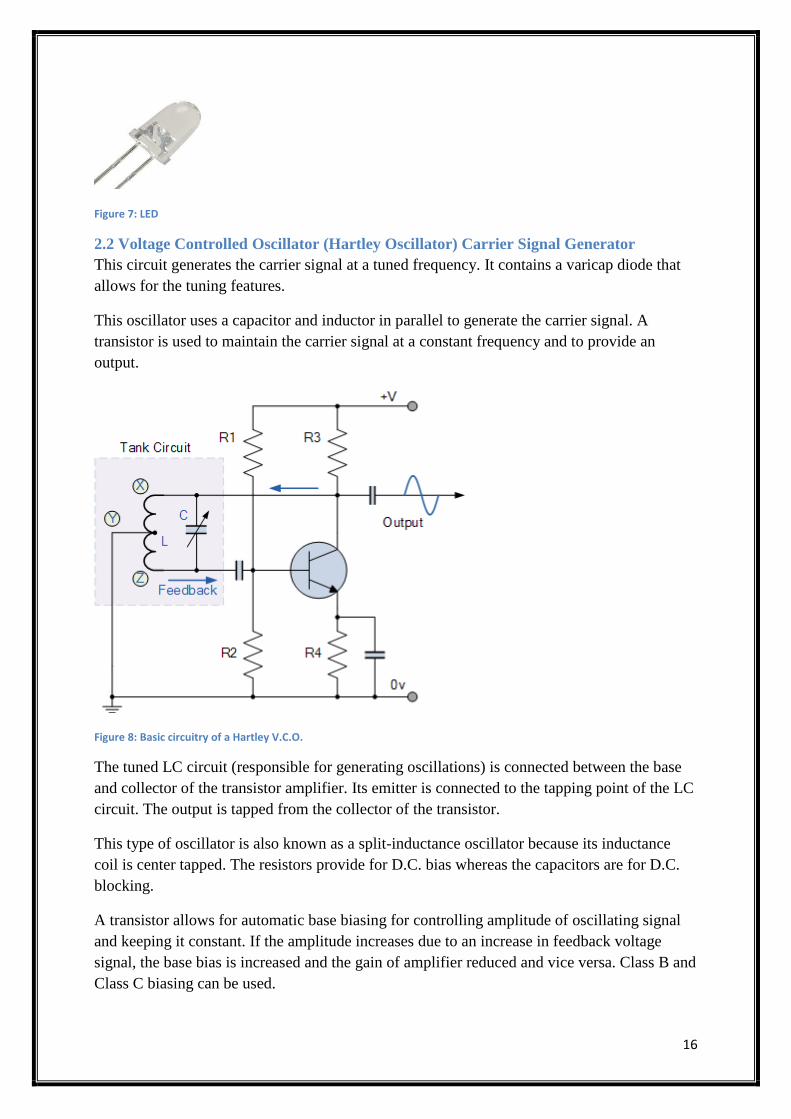
Figure 7: LED ........................................................................................................................... 16
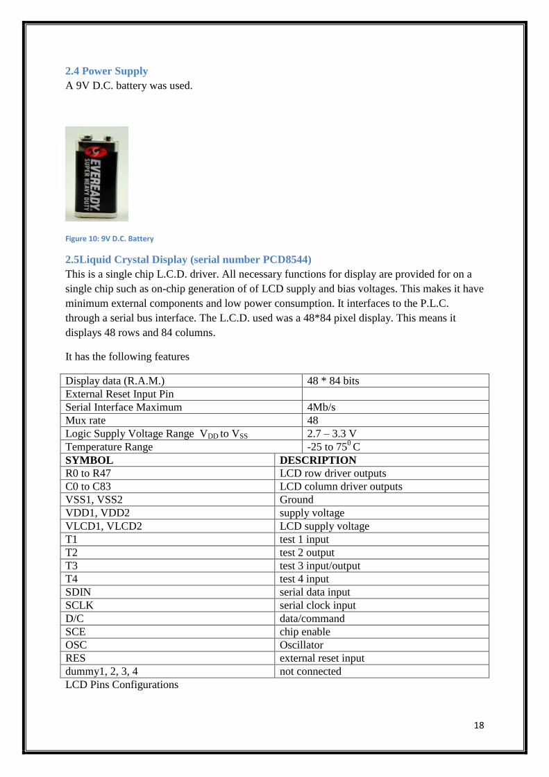
Figure 8: Basic circuitry of a Hartley V.C.O. .......................................................................... 16
Figure 9: Monopole Rubber Ducky antenna ............................................................................ 17
Figure 10: 9V D.C. Battery ...................................................................................................... 18
Figure 11: Connecting the fixed voltage regulator ................................................................... 20
Figure 12: Connecting the crystal oscillator ............................................................................ 21
Figure 13: Block Diagram of layout of circuitry ...................................................................... 24
Figure 14: Flowchart Diagram ................................................................................................. 37
List of Abbreviations
EEPROM – Electronically Erasable Programmable Read Only Memory
E.M.I. – Electromagnetic Interference
GHz – Gigahertz
ISP – In-System-Programming
L.C.D. – Liquid Crystal Display
L.E.D. – Light Emitting Diode
MHz - Megahertz
P.L.C. – Programmable Logic Control
P.W.M. – Pulse width modulation
R.F. – Radio Frequency (3 KHz – 3 GHz)
R.A.M. – Radar Absorbent Material
V.C.O. – Voltage Controlled Oscillator

vi
Contents
DECLARATION...................................................................................................................................... i
CERTIFICATION ....................................................................................................................................ii
DEDICATION ........................................................................................................................................ iii
ACKNOWLEDGEMENT ....................................................................................................................... iv
Table of Figures........................................................................................................................................ v
List of Abbreviations ................................................................................................................................ v
PROJECT ABSTRACT .......................................................................................................................... 8
CHAPTER ONE: INTRODUCTION ..................................................................................................... 9
1.0 BACKGROUND INFORMATION .............................................................................................. 9
1.0.1 Type “A” Device ............................................................................................................. 9
1.0.2 Type “B” Device or Intelligent Cellular Disabler Device ............................................... 9
1.0.3 Type “C” Device or Intelligent Beacon Disablers ........................................................... 9
1.0.4 Type “D” Device ............................................................................................................. 9
1.0.5 Type “E” Device............................................................................................................ 10
1.1 PROBLEM STATEMENT ......................................................................................................... 10
1.2 PROJECT JUSTIFICATION ...................................................................................................... 10
1.3 PROJECT AIMS AND OBJECTIVES ....................................................................................... 10
1.3.1 GLOBAL OBJECTIVES ..................................................................................................... 10
1.3.2 SPECIFIC OBJECTIVES .................................................................................................... 10
1.4 SCOPE ........................................................................................................................................ 10
CHAPTER TW0: LITERATURE REVIEW ........................................................................................ 11
2.0 OVERVIEW ................................................................................................................................ 11
2.1 Noise Generating Circuit ............................................................................................................. 11
2.1.0 Voltage Regulator ................................................................................................................. 11
2.1.1 Microcontroller ............................................................................................................................. 12
2.1.1.0 Microcontroller ATmega 328 ............................................................................................ 12
2.1.2 Resistors ............................................................................................................................... 14
2.1.3 Capacitors ............................................................................................................................. 14
2.1.4 Crystal Oscillator .................................................................................................................. 14
2.1.5 Light Emitting Diode ............................................................................................................ 15
2.2 Voltage Controlled Oscillator (Hartley Oscillator) Carrier Signal Generator ............................. 16
2.3 Monopole Antenna ...................................................................................................................... 17
2.4 Power Supply .............................................................................................................................. 18

vii
2.5 Liquid Crystal Display (serial number PCD8544) ...................................................................... 18
2.6 Tuner Circuit ............................................................................................................................... 19
CHAPTER THREE: METHODOLOGY .............................................................................................. 20
3.0 OVERVIEW ................................................................................................................................ 20
3.1 Powering the Jammer .................................................................................................................. 20
3.2 Generating Noise ......................................................................................................................... 20
3.3 Carrier Signal Generation ............................................................................................................ 21
3.4 Display of tuned frequency on L.C.D. .......................................................................................... 21
3.5 Transmission of jamming signal ................................................................................................. 23
3.6 Source Code ................................................................................................................................. 25
CHAPTER FOUR: RESULTS AND ANALYSIS ............................................................................... 36
4.0 OVERVIEW ................................................................................................................................ 36
4.1 Jamming of signal ........................................................................................................................ 36
4.2 Results ......................................................................................................................................... 36
4.3 CHALLENGES ........................................................................................................................... 37
CHAPTER FIVE: RECOMMENDATIONS AND CONCLUSION .................................................... 38
5.0 INTRODUCTION ....................................................................................................................... 38
5.1 RECOMMENDATIONS/FUTURE INPROVEMENTS ............................................................ 38
5.2 CONCLUSION ........................................................................................................................... 38
APPENDIX ........................................................................................................................................... 39
References ............................................................................................................................................. 39
Budget ................................................................................................................................................... 40
Time plan ............................................................................................................................................... 41

8
PROJECT ABSTRACT
Mobile telephony has revolutionized how we communicate with their major advantage being
portability of the mobile device and multiple services one can access. For instance, in Kenya
there is the money transfer service, M – Pesa.
However, their associated medium, radio-waves, have been found to have undesirable effects.
An example is interference with electromagnetic wave sensitive devices such as life-support
equipment in hospitals (such as the apnea monitor) and those in airplanes.
This necessitated a form of shielding with large and heavy full metal shielding coming into
use. However, this had severe limitations especially in airlines. In recent times, there have
been devised ways cheaper, less cumbersome ways of blocking these signals and effectively
curbing their associated interference.
In Kenya, there has been widespread extortion through mobile phones through the mobile
money transfer service, M-Pesa. Investigations have shown that the culprits usually are
inmates in correctional institutions.
This project is an attempt to curb these extortions by blocking a mobile service reception in
correctional extortions by using methods devised to block an electromagnetic signal through
Frequency Jamming. While doing so, it aims to achieve this in a portable, cost-effective and
flexible design.
The design uses an ATmega 328 8-bit PLC chip to generate noise. Its program code runs on
an Arduino Mega board. Using a resonator, it is able to obtain a timing signal of 64 MHz This
is signal is scaled using a frequency divider circuit in the P.L.C. to about 36 KHz. This
modulates a carrier signal generated by the Hartley Voltage Controlled Oscillator. The
VC.O.has a varactor diode that allows tuning of the frequency of the signal it generates. Thus,
a tuning circuit is necessary. A 48*84 L.C.D. display displays the tuned frequency. A
monopole omnidirectional rubber ducky antenna is used to transmit the jamming signal.
The above components are light and relatively affordable. The jammer is flexible in that it can
be tuned to jam a number of frequencies. Thus use of this design will help curb a vice, that of
extortion, that is threatening the existence of a technology that greatly benefits Kenyans.

9
CHAPTER ONE: INTRODUCTION
1.0 BACKGROUND INFORMATION
A Frequency Jammer is a device that transmits a signal at the same frequency at which a radio
transmitter operates. Frequency Jamming succeeds when a receiver device within its location
is disabled e.g. Radio or mobile phone.
Communication jamming devices were first developed and used for military purposes where
tactical commanders used R.F. communications to control their forces. Thus, an enemy would
aim at denying the successful transport of information from the sender to the receiver as a
battle tactic.
Presently, jammer devices are becoming civilian products with the increasing number of radio
device users where there is a need to disable such devices to avoid disruptions.
E.g. Libraries, Lecture Rooms, Churches, Meeting rooms, Hospitals etc.
There are different techniques for jamming as explained below
1.0.1 Type “A” Device
This overpowers the received signal using a stronger signal. It uses oscillators to transmit
“jamming signals” which block sending and receiving frequencies of devices such as cellular
phones and paging devices. When activated, they prevent cellular phones within their
designated area from receiving and transmitting calls. Type “A” device can operate in two
ways: brute force jamming or use of small amounts of interference. Brute force jams a wide
bandwidth and risks spilling over into unwanted frequencies. By using small amounts of
interference, jamming is basically in terms of small pockets hence a number of such pockets
are necessary.
1.0.2 Type “B” Device or Intelligent Cellular Disabler Device
This type jams by working as a detector. It also communicates with the cellular base station.
The device detects a mobile phone in its designed area (called a silent room) and signals the
base station. This is via software installed in the base station. The base station is signaled that
the cellular device is in a “quiet room” hence, should not establish communication. It is called
intelligent because it can sense emergency calls and can allow discriminative use of mobile
phones. This method is limited by need of mobile phone service providers to fully co-operate
with mobile phone manufacturers.
1.0.3 Type “C” Device or Intelligent Beacon Disablers
This device works as a beacon which commands any compatible terminal to disable its ringer
or operation. Its operation is limited by compatibility issues and need to be built on a separate
technology rather than the cellular technology such as the Bluetooth technology.
1.0.4 Type “D” Device
It is similar to Type “A” Device but with a receiver instead of a transmitter and always in
receive mode. When it detects a mobile phone in the “silent room”, it interacts and blocks the
phone by transmitting a jamming signal.

10
1.0.5 Type “E” Device
This uses E.M.I. suppression methods to turn a designated area into a Faraday cage. Basically,
the Faraday cage blocks electromagnetic radiation from entering or leaving the designated
area. However, it is quite labor intensive to construct.
1.1 PROBLEM STATEMENT
The project aims to create a jamming device that can be used on a certain frequency
bandwidth within a certain range (in terms of distance). This device should be portable. This
will eliminate the need of pre-conventional methods such as full metal cladding whose bulk
saw them have limited use. Also, its flexibility in terms of frequency will allow it to be used
for different signals which differ in terms of frequency. Thus, it overcomes a limitation
observed in (R.A.M.) Radar Absorbent Materials which could be used for principally the
same idea but for their case, a specific frequency. Its range of jamming (ideally 10 meters)
allows for selective blocking of a signal in terms of area. Since this project aims to curb
extortion by inmates, its range can cover the cell blocks only without interfering with the
administration block where the signal is needed.
1.2 PROJECT JUSTIFICATION
This is a cost-effective method and much cheaper as compared to other methods. For instance,
use of radar absorbent materials and full metal cladding. Its portability feature allows it to be
used in different settings such as hospital rooms, cell blocks and airplanes. Its flexibility
feature is also an added advantage as it can be tuned for different kinds of signals.
1.3 PROJECT AIMS AND OBJECTIVES
1.3.1 GLOBAL OBJECTIVES
To develop a Type “A” small interference jammer that will block a signal at a certain
frequency.
1.3.2 SPECIFIC OBJECTIVES
To fabricate a carrier generator
To assemble a noise generator and tuner circuit
To fabricate a transmission method
To assemble a display method
To code software that will be used to in displaying of frequencies.
1.4 SCOPE
This project will demonstrate how a jammer can block a signal using transmitted radio waves
of the range between 88.5 – 108.7 MHz Thus, one can use this project to block signals whose
frequencies fall in the fore mentioned frequency band.
11
CHAPTER TW0: LITERATURE REVIEW
2.0 OVERVIEW
A frequency jammer works by transmitting a signal at the same frequency of the received
signal. This frequency is the frequency of the carrier wave of the signal generated by the
jammer. A noise signal generated by the jammer is the frequency modulating signal of the
carrier signal. The frequency of the modulating signal (36 KHz) is beyond a human’s audible
range (2-20 KHz).
This chapter will center on the various components and circuitry of this project.
2.1 Noise Generating Circuit
2.1.0 Voltage Regulator
This is a device used to provide a fixed constant output voltage regardless of changes in input
voltage or load conditions. Voltage regulators are of two types: linear and switching.
A linear regulator uses an active pass device (BJT or MOSFET) which is controlled by a high
gain differential amplifier. Its output voltage is compared with a reference voltage and the
pass device adjusted accordingly to maintain a constant output voltage.
A switching voltage regulator converts the D.C. input voltage to a switched voltage. This
switched voltage is applied to a power switch (BJT/MOSFET). The filtered output voltage of
the power switch is fed to a circuit which controls the power switch ON and OFF times
resulting to a constant output voltage.
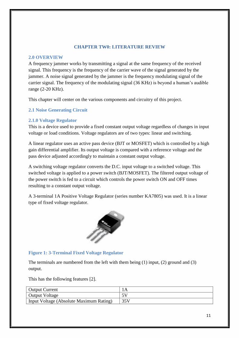
A 3-terminal 1A Positive Voltage Regulator (series number KA7805) was used. It is a linear
type of fixed voltage regulator.
Figure 1: 3-Terminal Fixed Voltage Regulator
The terminals are numbered from the left with them being (1) input, (2) ground and (3)
output.
This has the following features [2].
Output Current 1A
Output Voltage 5V
Input Voltage (Absolute Maximum Rating) 35V
12
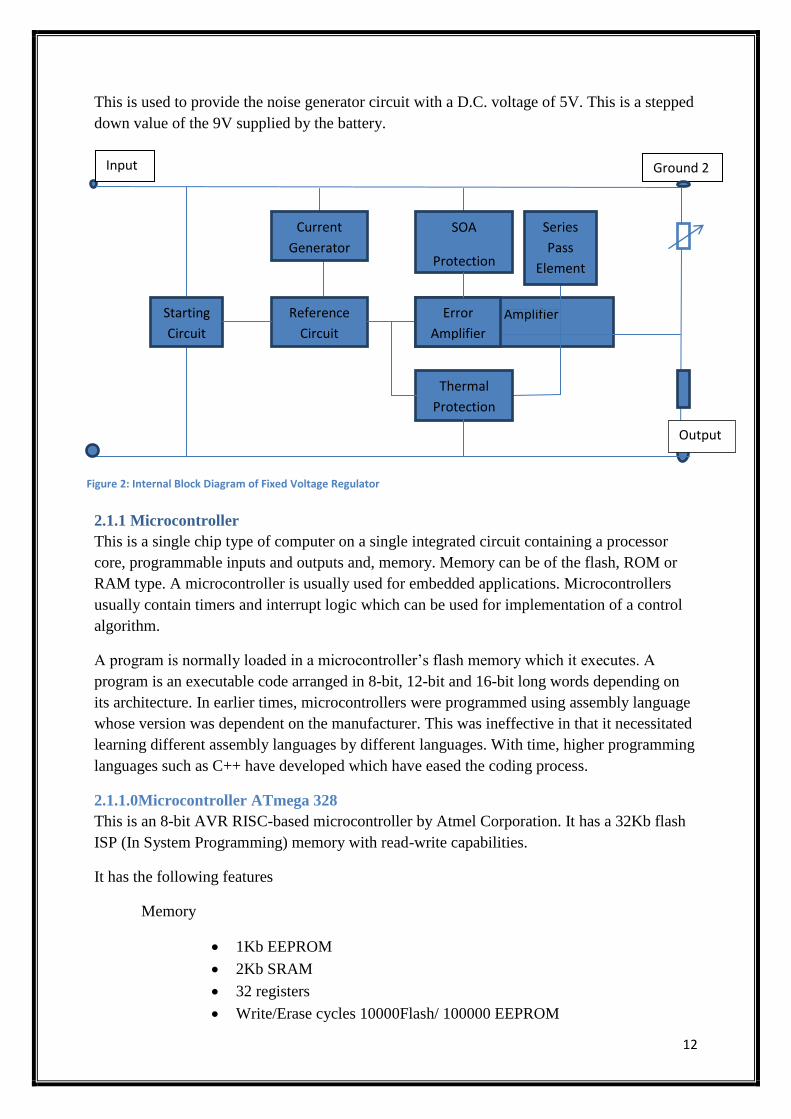
This is used to provide the noise generator circuit with a D.C. voltage of 5V. This is a stepped
down value of the 9V supplied by the battery.
2.1.1 Microcontroller
This is a single chip type of computer on a single integrated circuit containing a processor
core, programmable inputs and outputs and, memory. Memory can be of the flash, ROM or
RAM type. A microcontroller is usually used for embedded applications. Microcontrollers
usually contain timers and interrupt logic which can be used for implementation of a control
algorithm.
A program is normally loaded in a microcontroller’s flash memory which it executes. A
program is an executable code arranged in 8-bit, 12-bit and 16-bit long words depending on
its architecture. In earlier times, microcontrollers were programmed using assembly language
whose version was dependent on the manufacturer. This was ineffective in that it necessitated
learning different assembly languages by different languages. With time, higher programming
languages such as C++ have developed which have eased the coding process.
2.1.1.0Microcontroller ATmega 328
This is an 8-bit AVR RISC-based microcontroller by Atmel Corporation. It has a 32Kb flash
ISP (In System Programming) memory with read-write capabilities.
It has the following features
Memory
1Kb EEPROM
2Kb SRAM
32 registers
Write/Erase cycles 10000Flash/ 100000 EEPROM
Figure 2: Internal Block Diagram of Fixed Voltage Regulator
Ground 2
Error Amplifier Reference
Circuit
Thermal
Protection
Starting
Circuit
Current
Generator
SOA
Protection
Series
Pass
Element
Error
Amplifier
Input
Output

13
Data retention 20years at 85oC / 100 years at 25
oC
23 General Purpose Input/output lines
3 timers that are flexible and have compare modes
Internal and external interrupts
High Performance, low power 8-bit microcontroller
Operating Voltage 1.8 to 5.5 V
Speed 1.8 MHz
I/O 28-pin
Two 8-bit timers with separate pre-scaler and compare mode
One 16-bit timer with separate prescalar, compare mode and capture mode
Real time counter with separate oscillator
Six P.W.M. channels
Figure 3: ATmega 328 Pin Configuration
Figure 4: ATmega 328 P.L.C.

14
2.1.2 Resistors
This is a component that resists the flow of current. These were used to minimize the 5V from
the voltage regulator to a voltage that is safe for the various components such as the L.E.D. In
other words, they provided a safe operating current and voltage in the circuit.The blue L.E.D.
operates with 3V and was connected with a 220 Ω resistor with a tolerance of 5% to provide a
safe current of 22.3 mA. The crystal oscillator The L.C.D. was connected in series with 3
resistors of 600Ω 5% tolerance and two 1KΩ 5% tolerance to provide a total resistance of
2.6KΩ and a safe operating current of 1.9mA. Two 1KΩ resistors were connected with in
series with the crystal oscillator to provide a total resistance of 2kΩ and a safe operating
current of 2.5mA.
2.1.3 Capacitors
This is a component used to store energy. These were used to provide the microcontrollerwith
constant power. A capacitor of 33pF was used for this purpose. Two 27pF capacitors were
used as load capacitors for the crystal oscillator in order to provide a large gain for its
amplifier. Disturbances in power supply are due to the handling of the power source (9V
battery). Capacitors were also used in conjunction with the voltage regulator. A total of three
capacitors were used. Two capacitors were used in the mounting of the fixed voltage regulator
of the values 33pF and 10pF.
2.1.4 Crystal Oscillator
This is an electronic oscillator that uses the mechanical resonance of a piezoelectric crystal to
create an electric signal with a precise frequency; 16MHz for this case. This precision helps
them be used as timers. They are used to track time in quartz watches and provide a stable
clock signal for digital circuits. The quartz crystal is properly cut and mounted. A voltage is
then applied to an electrode on the crystal causing it to distort its shape. When this voltage is
removed, the quartz crystal regains its original shape and generates an electric field. Thus, it
behaves like a R.L.C. (resistance, inductance, and capacitance) circuit with a precise resonant
frequency.
Figure 5: 16MHz crystal oscillator
R L
Figure 6: Electrical Representation of Crystal Oscillator

15
The following components affect frequency of the oscillator: the series components
(equivalent series resistor, motional capacitor and motional inductor) and the shunt capacitor.
The oscillation frequency is obtained from the following formula:
F = 1/2π√LC
The following conditions have to be met in order for the crystal to oscillate:
Amplifier gain >= 1
A total phase shift across crystal of 360o
The following factors affect the crystal oscillation:
Shunt capacitance and equivalent series resistance is inversely proportional to
amplifier gain. Their increases cause a decrease in amplifier gain.
Load capacitors affect gain and phase margin. It is recommended to use 10pF and
33pF for the two load capacitors to generate the largest gain.
2.1.5 Light Emitting Diode
An L.E.D. is a diode (a semiconductor with a P-section and an N-section or P-N junction).
The P-section has extra holes and effectively has extra positive charges whereas the N-section
has extra electrons hence negatively charged. A diode can only conduct electricity in one
direction; in the direction opposite to that of electrons flow. If no voltage is applied to a diode,
the electrons in the N-section fill the holes in the P-section, at the junction, forming a
depletion layer. The depletion layer is a region where the semi-conductor is reverted to its
original condition of insulation as there are no free electrons and the holes are filled.
When a voltage is applied across the diode, the free electrons in the N-type are repelled by the
negative electrode towards the positive electrode. The holes in the P-section seemingly move
the other way. When the applied voltage is high enough (biasing voltage), the depletion layer
is broken and the electrons repelled. Reversing of voltage only serves to increase the depletion
layer and prevent flow of current.
When electrons move into the holes in the P-type, they fall from a conduction band to a lower
orbital and this accompanied by release of energy in form of a photon. This happens in all
diodes but in order for emitted light to be visible, its frequency has to fall within the visible
spectrum. The size of the gap between the conduction and a lower orbital determines the
frequency of the released photon.Hence,the larger the gap, the larger the frequency of the
released photon. The size of this gap is dependent on the type of material used to construct the
LED.
The LED used in this project is an LED that emits blue light when voltage is applied to it. It
can be made from the following materials: Zinc Selenide (ZnSe); Indium Gallium Nitride and
(InGaN). The shorter terminal is the cathode (-) with the anode (+) being the longer one.
16
Figure 7: LED
2.2 Voltage Controlled Oscillator (Hartley Oscillator) Carrier Signal Generator
This circuit generates the carrier signal at a tuned frequency. It contains a varicap diode that
allows for the tuning features.
This oscillator uses a capacitor and inductor in parallel to generate the carrier signal. A
transistor is used to maintain the carrier signal at a constant frequency and to provide an
output.
Figure 8: Basic circuitry of a Hartley V.C.O.
The tuned LC circuit (responsible for generating oscillations) is connected between the base
and collector of the transistor amplifier. Its emitter is connected to the tapping point of the LC
circuit. The output is tapped from the collector of the transistor.
This type of oscillator is also known as a split-inductance oscillator because its inductance
coil is center tapped. The resistors provide for D.C. bias whereas the capacitors are for D.C.
blocking.
A transistor allows for automatic base biasing for controlling amplitude of oscillating signal
and keeping it constant. If the amplitude increases due to an increase in feedback voltage
signal, the base bias is increased and the gain of amplifier reduced and vice versa. Class B and
Class C biasing can be used.

17
The advantages of this oscillator are that:
It allows control of the amplitude of the generated signal by controlled the voltage of
the feedback signal using the transistor.
The frequency of oscillations can be tuned.
2.3 Monopole Antenna
The antenna used in this project was a ¼-wave monopole antenna with 50-ohm impedance
and a 2dBi gain. It’s a rubber ducky type of monopole antenna which transmits in an
omnidirectional pattern. It consists of a rod-shaped conductor mounted on a conducting
surface called ground plane. The impedance is used for matching with the transmission
system. Its V.S.W.R. (Voltage Standing Wave Ratio) is low of less than 1.7 and a bandwidth
of 150 MHz around 916MHz as the center frequency.
Figure 9: Monopole Rubber Ducky antenna
18
2.4 Power Supply
A 9V D.C. battery was used.
Figure 10: 9V D.C. Battery
2.5Liquid Crystal Display (serial number PCD8544)
This is a single chip L.C.D. driver. All necessary functions for display are provided for on a
single chip such as on-chip generation of of LCD supply and bias voltages. This makes it have
minimum external components and low power consumption. It interfaces to the P.L.C.
through a serial bus interface. The L.C.D. used was a 48*84 pixel display. This means it
displays 48 rows and 84 columns.
It has the following features
Display data (R.A.M.) 48 * 84 bits
External Reset Input Pin
Serial Interface Maximum 4Mb/s
Mux rate 48
Logic Supply Voltage Range VDD to VSS 2.7 – 3.3 V
Temperature Range -25 to 750
C
SYMBOL DESCRIPTION
R0 to R47 LCD row driver outputs
C0 to C83 LCD column driver outputs
VSS1, VSS2 Ground
VDD1, VDD2 supply voltage
VLCD1, VLCD2 LCD supply voltage
T1 test 1 input
T2 test 2 output
T3 test 3 input/output
T4 test 4 input
SDIN serial data input
SCLK serial clock input
D/C data/command
SCE chip enable
OSC Oscillator
RES external reset input
dummy1, 2, 3, 4 not connected
LCD Pins Configurations

19
SYMBOL PARAMETER MIN. V MAX. V
VDD supply voltage -0.5 +7
VLCD supply voltage LCD -0.5 +10
LCD Parameters
2.6 Tuner Circuit
This is used to manually tune the V.C.O. to ensure it generates the carrier signal at a desired
frequency. It uses a potentiometer. This is by increasing or decreasing its capacitor using the
varactor diode. It has 1024 steps.
This circuit uses the following relation
F = 1/2π√LC
By increasing capacitance, frequency reduces and vice versa.

20
CHAPTER THREE: METHODOLOGY
3.0 OVERVIEW
The frequency jammer is made up of various different circuits. Their design is the focus of
this chapter.
The design process can be grouped as follows, on the basis of circuitry:
1. Powering the jammer
2. Noise Generation
3. Generating the carrier signal
4. Displaying the tuned frequency
5. Transmitting the jamming signal
Some of the above circuits function under the executed instructions loaded on the
microcontroller. Thus, the software bit will be displayed alongside them.
3.1 Powering the Jammer
A 9V battery is used to provide D.C. voltage. This is connected to a fixed voltage regulator
producing 5V. The positive terminal of the battery is connected to terminal 1 of the voltage
regulator and the second terminal to the negative terminal of the battery.
This is mounted as follows:
The output power is fed to the microcontroller via pin number 7, Vcc.
3.2 Generating Noise The crystal oscillator provides the ATmega 328 P.L.C. circuit with a timing signal of 16Mhz.
The microcontroller has a frequency divider circuit within it that scales down this signal from
16Mhz to 32Khz. This signal has to be beyond the audible range for humans that is 2KHz –
20Khz. This is used to modulate the V.C.O. carrier.
16MHz timer pulses from crystal resonator
100µF
KA7805 Input 9V
Output 5V to pin no.7
100µF
Figure 11: Connecting the fixed voltage regulator

21
36 KHz noise pulse obtained after frequency divider
The crystal resonator was mounted and connected to the microcontroller as follows:
3.3 Carrier Signal Generation
This is performed by the Hartley Oscillator. This has an L.C. circuit that produces an
oscillation. This oscillating signal is maintained at a constant frequency by use of a transistor
circuit. This transistor circuit is also used to tap this signal. Using the tuner circuit, the V.C.O.
is adjusted by adjusting the size of the varactor diode. This changes the size of capacitance
which is inversely proportional to frequency of the oscillating signal.
Its input is the signal (noise of 36KHz) from the microcontroller from the pin number 11. Its
power is from connecting to the PLC pin number 7.
3.4 Display of tuned frequency on L.C.D. The LCD was mounted and connected to the microcontroller as follows:
Its pin numbering 2 to 6 were connected in series with 1KΩ resistors to pins 1 to 5 of the
microcontroller respectively. LCD’s pin number 1 was connected to ground and number 8 to
number 7 of the microcontroller.
A software program mounted on the microcontroller calibrates the tuner circuit and outputs a
value to the 48*84 L.C.D. as shown below via a serial bus connector.
XTAL Pin no. 9
EXTAL Pin no. 10
C1 C1
Figure 12: Connecting the crystal oscillator

22
// All the pins can be changed from the default values...
PCD8544(unsigned char sclk = 3, /* clock (display pin 2) */
unsigned char sdin = 4, /* data-in (display pin 3) */
unsigned char dc = 5, /* data select (display pin 4) */
unsigned char reset = 6, /* reset (display pin 8) */
unsigned char sce = 7); /* enable (display pin 5) */
// Display initialization (dimensions in pixels)...
void begin(unsigned char width=84, unsigned char height=48, unsigned char
model=CHIP_PCD8544);
void stop();
// Erase everything on the display...
void clear();
voidclearLine(); // ...or just the current line
// Control the display's power state...
voidsetPower(bool on);
// For compatibility with the LiquidCrystal library...
void display();
voidnoDisplay();
// Activate white-on-black mode (whole display)...
voidsetInverse(bool inverse);
// Place the cursor at the start of the current line...

23
void home();
// Place the cursor at position (column, line)...
voidsetCursor(unsigned char column, unsigned char line);
As the VCO signal frequency is tuned it is displayed as follows:
void loop()
sensorValue = analogRead(analogInPin);
// map it to the range of the analog out:
// outputValue = map(sensorValue, 0, 410, 0, 410);
// lcd.clear();
lcd.setCursor(0, 0);
lcd.print("FREQUENCY JAMMER");
lcd.setCursor(25, 4);
lcd.print( 87.5+(sensorValue/49.90243902439024));
lcd.print("Mhz");
delay(10);
lcd.clear();
3.5 Transmission of jamming signal
The modulating signal (noise) is the input to the oscillator. This modulates the carrier signal
generated by the Hartley V.C.O. The modulated signal is then fed to the R.F. amplifier of the
antenna for amplification of its power suitable for transmission. It is then fed to the monopole

24
antenna which transmits the signal. The signal is applied between the ground plane and lower
end of the monopole.
Varactor diode
FM 87.5-108
Mhz
Voltage Controlled oscillator
(VCO)
Frequency Display
LCD
PLC
Noise Generator
Signal >20 KHz
9v-5v
Power regulator
circuit
7805
RF Amplifier
Antenna
Figure 13: Block Diagram of layout of circuitry

25
3.6 Source Code #include <PCD8544.h>
#ifndef PCD8544_H
#define PCD8544_H
#if ARDUINO < 100
#include <WProgram.h>
#else
#include <Arduino.h>
#endif
// Chip variants supported...
#define CHIP_PCD8544 0
#define CHIP_ST7576 1
class PCD8544: public Print
public:
// All the pins can be changed from the default values...
PCD8544(unsigned char sclk = 3, /* clock (display pin 2) */
unsigned char sdin = 4, /* data-in (display pin 3) */
unsigned char dc = 5, /* data select (display pin 4) */
unsigned char reset = 6, /* reset (display pin 8) */
unsigned char sce = 7); /* enable (display pin 5) */
// Display initialization (dimensions in pixels)...
void begin(unsigned char width=84, unsigned char height=48, unsigned char model=CHIP_PCD8544);
void stop();
// Erase everything on the display...
void clear();
voidclearLine(); // ...or just the current line
// Control the display's power state...
voidsetPower(bool on);

26
// For compatibility with the LiquidCrystal library...
void display();
voidnoDisplay();
// Activate white-on-black mode (whole display)...
voidsetInverse(bool inverse);
// Place the cursor at the start of the current line...
void home();
// Place the cursor at position (column, line)...
voidsetCursor(unsigned char column, unsigned char line);
// Assign a user-defined glyph (5x8) to an ASCII character (0-31)...
voidcreateChar(unsigned char chr, const unsigned char *glyph);
// Write an ASCII character at the current cursor position (7-bit)...
#if ARDUINO < 100
virtual void write(uint8_t chr);
#else
virtualsize_t write(uint8_t chr);
#endif
// Draw a bitmap at the current cursor position...
voiddrawBitmap(const unsigned char *data, unsigned char columns, unsigned char lines);
// Draw a chart element at the current cursor position...
voiddrawColumn(unsigned char lines, unsigned char value);
private:
unsigned char pin_sclk;
unsigned char pin_sdin;
unsigned char pin_dc;
unsigned char pin_reset;
unsigned char pin_sce;

27
// The size of the display, in pixels...
unsigned char width;
unsigned char height;
// Current cursor position...
unsigned char column;
unsigned char line;
// User-defined glyphs (below the ASCII space character)...
const unsigned char *custom[' '];
// Send a command or data to the display...
void send(unsigned char type, unsigned char data);
;
#endif /* PCD8544_H */
/* vim: set expandtabts=4 sw=4: */
static PCD8544 lcd;
constintanalogInPin = A0; // Analog input pin that the potentiometer is attached to
floatsensorValue = 0; // value read from the pot
intoutputValue = 0; // value output to the PWM (analog out)
void setup()
lcd.begin(84, 48);
lcd.clear();
void loop()
sensorValue = analogRead(analogInPin);
// map it to the range of the analog out:
// outputValue = map(sensorValue, 0, 410, 0, 410);

28
// lcd.clear();
lcd.setCursor(0, 0);
lcd.print("FREQUENCY JAMMER");
lcd.setCursor(25, 4);
lcd.print( 87.5+(sensorValue/49.90243902439024));
lcd.print("Mhz");
delay(10);
lcd.clear();
PCD8544::PCD8544(unsigned char sclk, unsigned char sdin,
unsigned char dc, unsigned char reset,
unsigned char sce):
pin_sclk(sclk),
pin_sdin(sdin),
pin_dc(dc),
pin_reset(reset),
pin_sce(sce)
void PCD8544::begin(unsigned char width, unsigned char height, unsigned char model)
this->width = width;
this->height = height;
this->column = 0;
this->line = 0;
// Sanitize the custom glyphs...
memset(this->custom, 0, sizeof(this->custom));
// All pins are outputs (these displays cannot be read)...

29
pinMode(this->pin_sclk, OUTPUT);
pinMode(this->pin_sdin, OUTPUT);
pinMode(this->pin_dc, OUTPUT);
pinMode(this->pin_reset, OUTPUT);
pinMode(this->pin_sce, OUTPUT);
// Reset the controller state...
digitalWrite(this->pin_reset, HIGH);
digitalWrite(this->pin_sce, HIGH);
digitalWrite(this->pin_reset, LOW);
delay(100);
digitalWrite(this->pin_reset, HIGH);
// Set the LCD parameters...
this->send(PCD8544_CMD, 0x21); // extended instruction set control (H=1)
this->send(PCD8544_CMD, 0x13); // bias system (1:48)
if (model == CHIP_ST7576)
this->send(PCD8544_CMD, 0xe0); // higher Vop, too faint at default
this->send(PCD8544_CMD, 0x05); // partial display mode
else
this->send(PCD8544_CMD, 0xc2); // default Vop (3.06 + 66 * 0.06 = 7V)
this->send(PCD8544_CMD, 0x20); // extended instruction set control (H=0)
this->send(PCD8544_CMD, 0x09); // all display segments on
// Clear RAM contents...
this->clear();
// Activate LCD...
this->send(PCD8544_CMD, 0x08); // display blank
this->send(PCD8544_CMD, 0x0c); // normal mode (0x0d = inverse mode)

30
delay(100);
// Place the cursor at the origin...
this->send(PCD8544_CMD, 0x80);
this->send(PCD8544_CMD, 0x40);
void PCD8544::stop()
this->clear();
this->setPower(false);
void PCD8544::clear()
this->setCursor(0, 0);
for (unsigned short i = 0; i < this->width * (this->height/8); i++)
this->send(PCD8544_DATA, 0x00);
this->setCursor(0, 0);
void PCD8544::clearLine()
this->setCursor(0, this->line);
for (unsigned char i = 0; i < this->width; i++)
this->send(PCD8544_DATA, 0x00);
this->setCursor(0, this->line);
void PCD8544::setPower(bool on)
31
this->send(PCD8544_CMD, on ? 0x20 : 0x24);
inline void PCD8544::display()
this->setPower(true);
inline void PCD8544::noDisplay()
this->setPower(false);
void PCD8544::setInverse(bool inverse)
this->send(PCD8544_CMD, inverse ? 0x0d : 0x0c);
void PCD8544::home()
this->setCursor(0, this->line);
void PCD8544::setCursor(unsigned char column, unsigned char line)
this->column = (column % this->width);
this->line = (line % (this->height/9 + 1));
this->send(PCD8544_CMD, 0x80 | this->column);
this->send(PCD8544_CMD, 0x40 | this->line);
void PCD8544::createChar(unsigned char chr, const unsigned char *glyph)

32
// ASCII 0-31 only...
if (chr>= ' ')
return;
this->custom[chr] = glyph;
#if ARDUINO < 100
void PCD8544::write(uint8_t chr)
#else
size_t PCD8544::write(uint8_t chr)
#endif
// ASCII 7-bit only...
if (chr>= 0x80)
#if ARDUINO < 100
return;
#else
return 0;
#endif
const unsigned char *glyph;
unsigned char pgm_buffer[5];
if (chr>= ' ')
// Regular ASCII characters are kept in flash to save RAM...
memcpy_P(pgm_buffer, &charset[chr - ' '], sizeof(pgm_buffer));
glyph = pgm_buffer;

33
else
// Custom glyphs, on the other hand, are stored in RAM...
if (this->custom[chr])
glyph = this->custom[chr];
else
// Default to a space character if unset...
memcpy_P(pgm_buffer, &charset[0], sizeof(pgm_buffer));
glyph = pgm_buffer;
// Output one column at a time...
for (unsigned char i = 0; i < 5; i++)
this->send(PCD8544_DATA, glyph[i]);
// One column between characters...
this->send(PCD8544_DATA, 0x00);
// Update the cursor position...
this->column = (this->column + 6) % this->width;
if (this->column == 0)
this->line = (this->line + 1) % (this->height/9 + 1);
#if ARDUINO >= 100
return 1;
#endif
void PCD8544::drawBitmap(const unsigned char *data, unsigned char columns, unsigned char lines)

34
unsigned char scolumn = this->column;
unsigned char sline = this->line;
// The bitmap will be clipped at the right/bottom edge of the display...
unsigned char mx = (scolumn + columns > this->width) ? (this->width - scolumn) : columns;
unsigned char my = (sline + lines > this->height/8) ? (this->height/8 - sline) : lines;
for (unsigned char y = 0; y < my; y++)
this->setCursor(scolumn, sline + y);
for (unsigned char x = 0; x < mx; x++)
this->send(PCD8544_DATA, data[y * columns + x]);
// Leave the cursor in a consistent position...
this->setCursor(scolumn + columns, sline);
void PCD8544::drawColumn(unsigned char lines, unsigned char value)
unsigned char scolumn = this->column;
unsigned char sline = this->line;
// Keep "value" within range...
if (value > lines*8)
value = lines*8;
// Find the line where "value" resides...
unsigned char mark = (lines*8 - 1 - value)/8;
// Clear the lines above the mark...
for (unsigned char line = 0; line < mark; line++)
this->setCursor(scolumn, sline + line);

35
this->send(PCD8544_DATA, 0x00);
// Compute the byte to draw at the "mark" line...
unsigned char b = 0xff;
for (unsigned char i = 0; i < lines*8 - mark*8 - value; i++)
b <<= 1;
this->setCursor(scolumn, sline + mark);
this->send(PCD8544_DATA, b);
// Fill the lines below the mark...
for (unsigned char line = mark + 1; line < lines; line++)
this->setCursor(scolumn, sline + line);
this->send(PCD8544_DATA, 0xff);
// Leave the cursor in a consistent position...
this->setCursor(scolumn + 1, sline);
void PCD8544::send(unsigned char type, unsigned char data)
digitalWrite(this->pin_dc, type);
digitalWrite(this->pin_sce, LOW);
shiftOut(this->pin_sdin, this->pin_sclk, MSBFIRST, data);
digitalWrite(this->pin_sce, HIGH);
/* vim: set expandtabts=4 sw=4: */

36
CHAPTER FOUR: RESULTS AND ANALYSIS
4.0 OVERVIEW
This chapter explains the working of the whole circuit.
The jammer is powered by the 9V battery D.C. source. Using a voltage regulator, the 9V are
stepped down to 5v for the various components.
The crystal oscillator acts as a resonator and provides a 16 MHz signal to the microcontroller.
This has a frequency dividing circuit that scales down this high frequency to 36 KHz. This is
noise and is then fed to the Hartley VCO oscillator.
The Hartley oscillator generates a carrier signal of fixed amplitude. Its frequency is varied
using a potentiometer in the tuner. The frequency band of this oscillator is within the FM
bandwidth.
As the frequency is tuned, it is, at the same time, displayed on the LCD. The LED lights up to
assist with visibility.
The modulated signal is then fed to the R.F. Amplifier for amplification of its transmission
power.
It is then fed to the monopole antenna where it is transmitted.
4.1 Jamming of signal The jamming signal is transmitted at a particular tuned frequency. If this coincides with the
signal a device (radio) is receiving, it will be received on the basis that it is stronger than the
remote signal. This is because of proximity of transmission. Once received, it is demodulated
and the modulating signal (noise) is obtained. As the frequency of the signal (36 KHz) is
beyond the audible range of 20 KHz, nothing will be heard.
4.2 Results The jammer was able to jam signals of the following frequencies 105.2 and 106.3MHz at a
range of 5meters.

37
4.3 CHALLENGES
This jamming device only transmitted a jamming signal and had poor frequency selectivity.
This is a type “A” small interference jammer. Hence, in order to simultaneously block signals
with different frequencies falling within the relevant band, a number of similar such devices
are needed.
Calibration of the tuner circuit to coincide with the jammed frequency was an issue. Also, it
was difficult to block all frequencies within the applicable bandwidth.
Obtaining components such as a VCO chip proved difficult.
Start
Clear LCD memory
Display User name
Initialize Up-down
counter
Lock attained?
Display current frequency
f=87.5-(Capacitor dial value/20.5)
Clear LCD memory
Ignore values
97.4Mhz>f<108.1Mhz
No
Yes
Figure 14: Flowchart Diagram

38
CHAPTER FIVE: RECOMMENDATIONS AND CONCLUSION
5.0 INTRODUCTION
This chapter outlines some improvements that can be done to the jammer
5.1 RECOMMENDATIONS/FUTURE INPROVEMENTS
The tuner circuit should be better calibrated to make it more precise. This will also assist in
blocking frequencieswithin the applicable frequency band.
A higher powered RF amp can be used to improve the range of the jammer.
5.2 CONCLUSION
The aim of the project which was to build a jammer that was portable and flexible in terms of
frequency was achieved.
From the results, this was achieved with signals of frequencies 105.2 and 106.3 MHz blocked
within a range of 5m.

39
APPENDIX
References
[1] Mobile & Personal Communications Committee of the Radio Advisory Board of Canada
“Use of Jammer and Disabler Devices for blocking PCS, Cellular and Related Services”
http://www.rabc.ottawa.on.ca/e/Files/01pub3.pdf
[2] www.datasheetcatalog.com
[3] PCD8544 48 * 84 pixels matrix LCD controller / driver datasheet
[4] KA7805 3-terminal Positive Voltage Regulator datasheet
[5] Atmel ATmega 328 micrcontroller datasheet
40
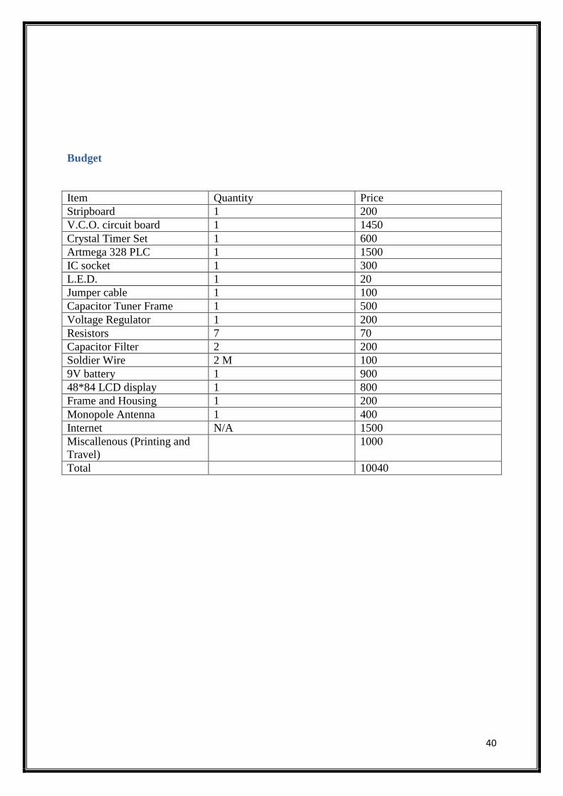
Budget
Item Quantity Price
Stripboard 1 200
V.C.O. circuit board 1 1450
Crystal Timer Set 1 600
Artmega 328 PLC 1 1500
IC socket 1 300
L.E.D. 1 20
Jumper cable 1 100
Capacitor Tuner Frame 1 500
Voltage Regulator 1 200
Resistors 7 70
Capacitor Filter 2 200
Soldier Wire 2 M 100
9V battery 1 900
48*84 LCD display 1 800
Frame and Housing 1 200
Monopole Antenna 1 400
Internet N/A 1500
Miscallenous (Printing and
Travel)
1000
Total 10040
41
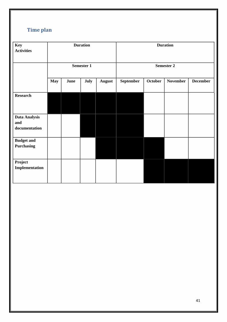
Time plan
Key Activities
Duration Duration
Semester 1 Semester 2
May June July August September October November December
Research
Data Analysis
and
documentation
Budget and Purchasing
Project Implementation