
Collection of Solved Feedback Ampli fier...
37
c ° Copyright 2009. W. Marshall Leach, Jr., Professor, Georgia Institute of Technology, School of Electrical and Computer Engineering. Collection of Solved Feedback Amplifier Problems This document contains a collection of solved feedback amplifier problems involving one or more active devices. The solutions make use of a graphical tool for solving simultaneous equations that is called the Mason Flow Graph (also called the Signal Flow Graph). When set up properly, the graph can be used to obtain by inspection the gain of a feedback amplifier, its input resistance, and its output resistance without solving simultaneous equations. Some background on how the equations are written and how the flow graph is used to solve them can be found at http://users.ece.gatech.edu/~mleach/ece3050/notes/feedback/fdbkamps.pdf The gain of a feedback amplifier is usually written in the form A ÷ (1 + bA), where A is the gain with feedback removed and b is the feedback factor. In order for this equation to apply to the four types of feedback amplifiers, the input and output variables must be chosen correctly. For amplifiers that employ series summing at the input (alson called voltage summing), the input variable must be a voltage. In this case, the source is modeled as a Thévenin equivalent circuit. For amplifiers that employ shunt summing at the input (also called current summing), the input variable must be a current. In this case, the source is modeled as a Norton equivalent circuit. When the output sampling is in shunt with the load (also called voltage sampling), the output variable must be a voltage. When the output sampling is in series with the load (also called current sampling), the output variable must be a current. These conventions are followed in the following examples. The quantity Ab is called the loop gain. For the feedback to be negative, the algebraic sign of Ab must be positive. If Ab is negative the feedback is positive and the amplifier is unstable. Thus if A is positive, b must also be positive. If A is negative, b must be negative. The quantity (1 + Ab) is called the amount of feedback. It is often expressed in dB with the relation 20 log (1 + Ab). For series summing at the input, the expression for the input resistance is of the form R IN × (1 + bA), where R IN is the input resistance without feedback. For shunt summing at the input, the expression for the input resistance is of the form R IN ÷ (1 + bA). For shunt sampling at the output, the expression for the output resistance is of the form R O ÷ (1 + bA), where R O is the output resistance without feedback. To calculate this in the examples, a test current source is added in shunt with the load. For series sampling at the output, the expression for the output resistance is of the form R O × (1 + bA). To calculate this in the examples, a test voltage source is added in series with the load. Most texts neglect the feedforward gain through the feedback network in calculating the forward gain A. When the flow graph is used for the analysis, this feedforward gain can easily be included in the analysis without complicating the solution. This is done in all of the examples here. The dc bias sources in the examples are not shown. It is assumed that the solutions for the dc voltages and currents in the circuits are known. In addition, it is assumed that any dc coupling capacitors in the circuits are ac short circuits for the small-signal analysis. Series-Shunt Example 1 Figure 1(a) shows the ac signal circuit of a series-shunt feedback amplifier. The input variable is v 1 and the output variable is v 2 . The input signal is applied to the gate of M 1 and the feedback signal is applied to the source of M 1 . Fig. 1(b) shows the circuit with feedback removed. A test current source i t is added in shunt with the output to calculate the output resistance R B . The feedback at the source of M 1 is modeled by a Thévenin equivalent circuit. The feedback factor or feedback ratio b is the coefficient of v 2 in this source, i.e. b = R 1 / (R 1 + R 3 ). The circuit values are g m =0.001 S, r s = g −1 m =1kΩ, r 0 = ∞, R 1 =1kΩ, R 2 = 10 kΩ, R 3 =9kΩ, R 4 =1kΩ, and R 5 = 100 kΩ. The following equations can be written for the circuit with feedback removed: i d1 = G m1 v a G m1 = 1 r s1 + R 1 kR 3 v a = v 1 − v ts1 v ts1 = R 1 R 1 + R 3 v 2 i d2 = −g m v tg2 1
Transcript of Collection of Solved Feedback Ampli fier...
c° Copyright 2009. W. Marshall Leach, Jr., Professor, Georgia Institute of Technology, School of Electricaland Computer Engineering.
Collection of Solved Feedback Amplifier ProblemsThis document contains a collection of solved feedback amplifier problems involving one or more activedevices. The solutions make use of a graphical tool for solving simultaneous equations that is called theMason Flow Graph (also called the Signal Flow Graph). When set up properly, the graph can be used toobtain by inspection the gain of a feedback amplifier, its input resistance, and its output resistance withoutsolving simultaneous equations. Some background on how the equations are written and how the flow graphis used to solve them can be found at
http://users.ece.gatech.edu/~mleach/ece3050/notes/feedback/fdbkamps.pdf
The gain of a feedback amplifier is usually written in the form A ÷ (1 + bA), where A is the gain withfeedback removed and b is the feedback factor. In order for this equation to apply to the four types offeedback amplifiers, the input and output variables must be chosen correctly. For amplifiers that employseries summing at the input (alson called voltage summing), the input variable must be a voltage. In thiscase, the source is modeled as a Thévenin equivalent circuit. For amplifiers that employ shunt summing atthe input (also called current summing), the input variable must be a current. In this case, the source ismodeled as a Norton equivalent circuit. When the output sampling is in shunt with the load (also calledvoltage sampling), the output variable must be a voltage. When the output sampling is in series with theload (also called current sampling), the output variable must be a current. These conventions are followedin the following examples.The quantity Ab is called the loop gain. For the feedback to be negative, the algebraic sign of Ab must
be positive. If Ab is negative the feedback is positive and the amplifier is unstable. Thus if A is positive, bmust also be positive. If A is negative, b must be negative. The quantity (1 +Ab) is called the amount offeedback. It is often expressed in dB with the relation 20 log (1 +Ab).For series summing at the input, the expression for the input resistance is of the form RIN × (1 + bA),
where RIN is the input resistance without feedback. For shunt summing at the input, the expression forthe input resistance is of the form RIN ÷ (1 + bA). For shunt sampling at the output, the expression forthe output resistance is of the form RO ÷ (1 + bA), where RO is the output resistance without feedback. Tocalculate this in the examples, a test current source is added in shunt with the load. For series sampling atthe output, the expression for the output resistance is of the form RO × (1 + bA). To calculate this in theexamples, a test voltage source is added in series with the load.Most texts neglect the feedforward gain through the feedback network in calculating the forward gain A.
When the flow graph is used for the analysis, this feedforward gain can easily be included in the analysiswithout complicating the solution. This is done in all of the examples here.The dc bias sources in the examples are not shown. It is assumed that the solutions for the dc voltages
and currents in the circuits are known. In addition, it is assumed that any dc coupling capacitors in thecircuits are ac short circuits for the small-signal analysis.
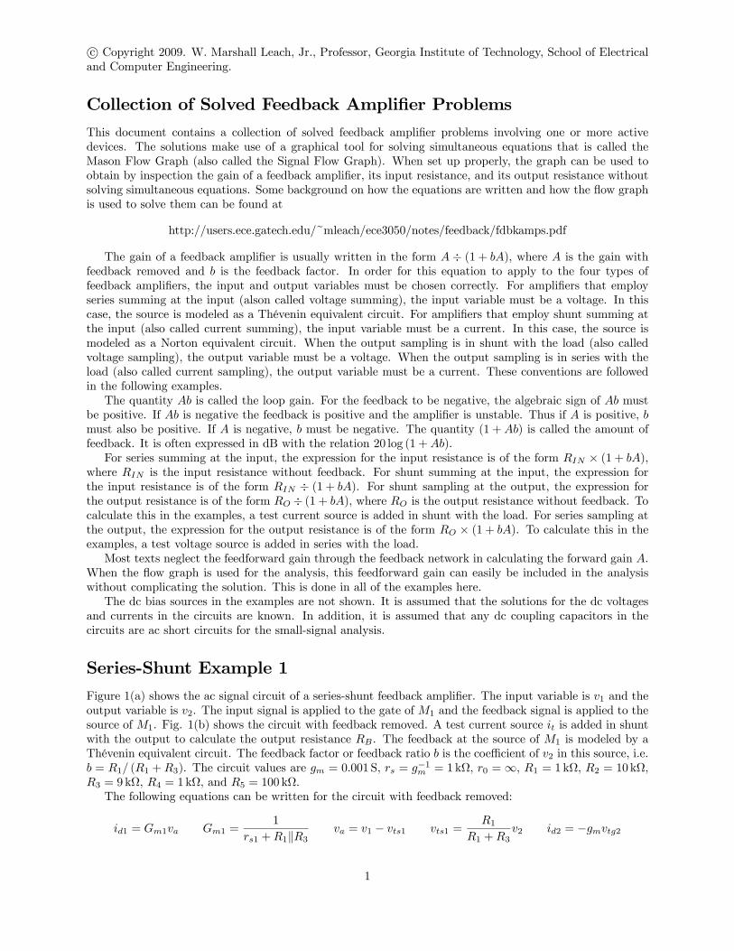
Series-Shunt Example 1Figure 1(a) shows the ac signal circuit of a series-shunt feedback amplifier. The input variable is v1 and theoutput variable is v2. The input signal is applied to the gate of M1 and the feedback signal is applied to thesource of M1. Fig. 1(b) shows the circuit with feedback removed. A test current source it is added in shuntwith the output to calculate the output resistance RB. The feedback at the source of M1 is modeled by aThévenin equivalent circuit. The feedback factor or feedback ratio b is the coefficient of v2 in this source, i.e.b = R1/ (R1 +R3). The circuit values are gm = 0.001 S, rs = g−1m = 1kΩ, r0 =∞, R1 = 1kΩ, R2 = 10kΩ,R3 = 9kΩ, R4 = 1kΩ, and R5 = 100 kΩ.The following equations can be written for the circuit with feedback removed:
id1 = Gm1va Gm1 =1
rs1 +R1kR3 va = v1 − vts1 vts1 =R1
R1 +R3v2 id2 = −gmvtg2
1
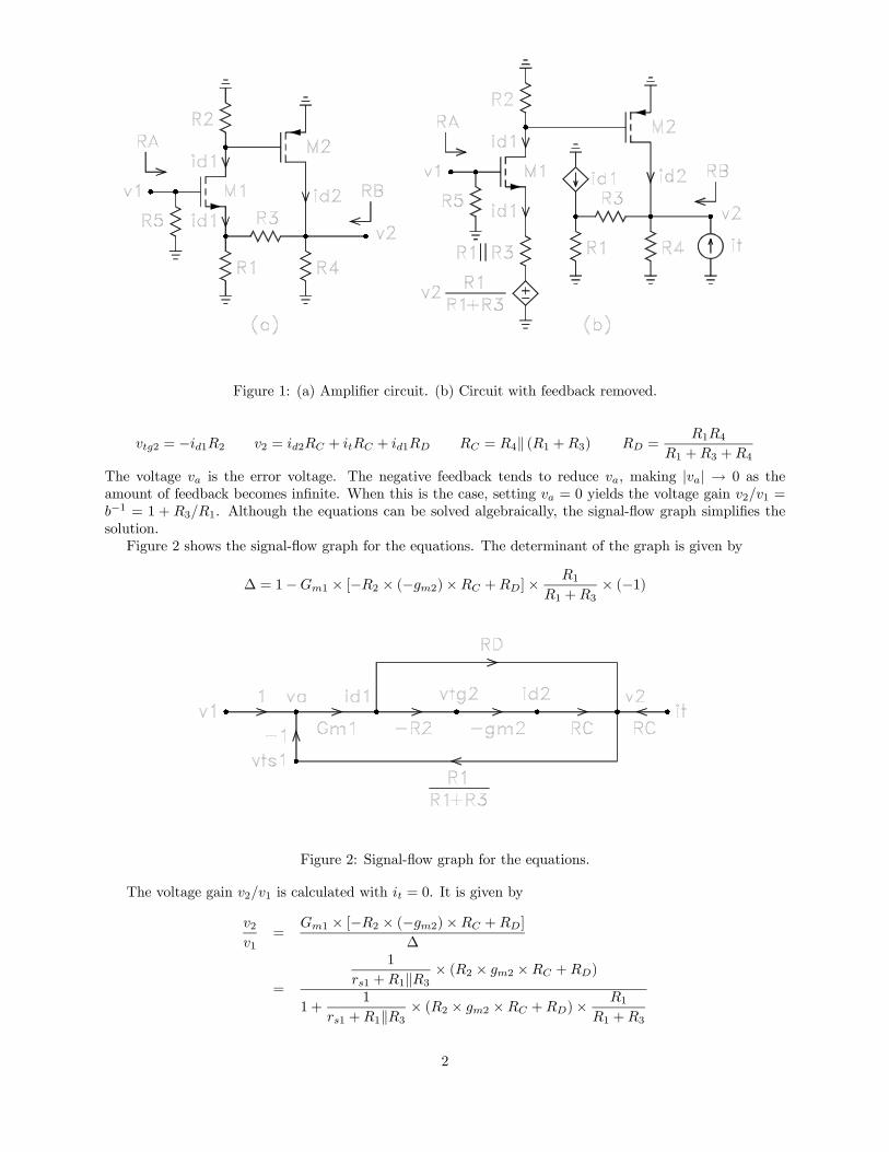
Figure 1: (a) Amplifier circuit. (b) Circuit with feedback removed.
vtg2 = −id1R2 v2 = id2RC + itRC + id1RD RC = R4k (R1 +R3) RD =R1R4
R1 +R3 +R4
The voltage va is the error voltage. The negative feedback tends to reduce va, making |va| → 0 as theamount of feedback becomes infinite. When this is the case, setting va = 0 yields the voltage gain v2/v1 =b−1 = 1 + R3/R1. Although the equations can be solved algebraically, the signal-flow graph simplifies thesolution.Figure 2 shows the signal-flow graph for the equations. The determinant of the graph is given by
∆ = 1−Gm1 × [−R2 × (−gm2)×RC +RD]× R1R1 +R3
× (−1)
Figure 2: Signal-flow graph for the equations.
The voltage gain v2/v1 is calculated with it = 0. It is given by
v2v1
=Gm1 × [−R2 × (−gm2)×RC +RD]
∆
=
1
rs1 +R1kR3 × (R2 × gm2 ×RC +RD)
1 +1
rs1 +R1kR3 × (R2 × gm2 ×RC +RD)× R1R1 +R3
2
This is of the formv2v1=
A
1 +Ab
whereA =
1
rs1 +R1kR3 × (R2 × gm2 ×RC +RD) = 4.83
b =R1
R1 +R3= 0.1
Note that Ab is dimensionless. Numerical evaluation yields
v2v1=
4.83
1 + 0.483= 3.26
The output resistance RB is calculated with v1 = 0. It is given by
RB =v2it=
RC
∆=
RC
1 +Ab= 613Ω
Note that the feedback tends to decrease RB. Because the gate current of M1 is zero, the input resistanceis RA = R5 = 100kΩ.
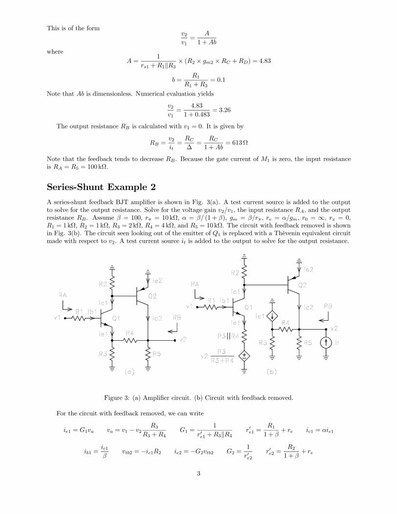
Series-Shunt Example 2A series-shunt feedback BJT amplifier is shown in Fig. 3(a). A test current source is added to the outputto solve for the output resistance. Solve for the voltage gain v2/v1, the input resistance RA, and the outputresistance RB. Assume β = 100, rπ = 10kΩ, α = β/ (1 + β), gm = β/rπ, re = α/gm, r0 = ∞, rx = 0,R1 = 1kΩ, R2 = 1kΩ, R3 = 2kΩ, R4 = 4kΩ, and R5 = 10kΩ. The circuit with feedback removed is shownin Fig. 3(b). The circuit seen looking out of the emitter of Q1 is replaced with a Thévenin equivalent circuitmade with respect to v2. A test current source it is added to the output to solve for the output resistance.
Figure 3: (a) Amplifier circuit. (b) Circuit with feedback removed.
For the circuit with feedback removed, we can write
ie1 = G1va va = v1 − v2R3
R3 +R4G1 =
1
r0e1 +R3kR4 r0e1 =R11 + β
+ re ic1 = αie1
ib1 =ic1β
vtb2 = −ic1R2 ie2 = −G2vtb2 G2 =1
r0e2r0e2 =
R21 + β
+ re
3
ic2 = αie2 v2 = ic2Ra + itRa + ie1Rb Ra = R5k (R3 +R4) Rb =R3R5
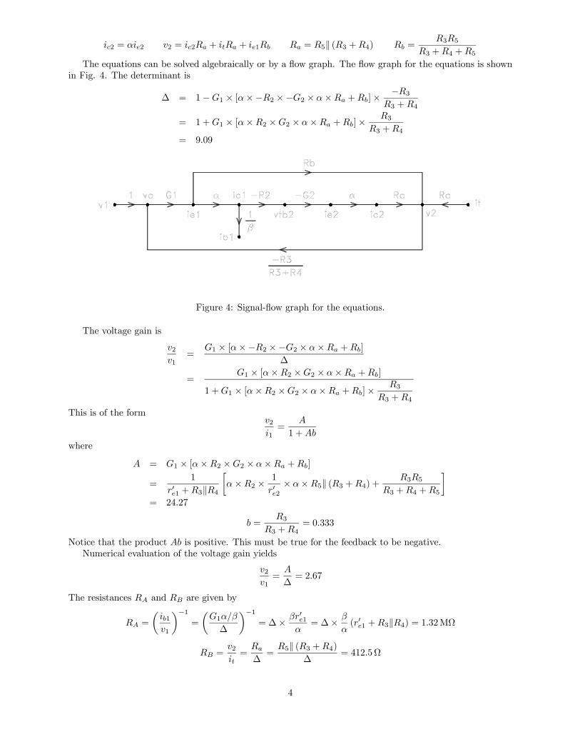
R3 +R4 +R5The equations can be solved algebraically or by a flow graph. The flow graph for the equations is shown
in Fig. 4. The determinant is
∆ = 1−G1 × [α×−R2 ×−G2 × α×Ra +Rb]× −R3R3 +R4
= 1 +G1 × [α×R2 ×G2 × α×Ra +Rb]× R3R3 +R4
= 9.09
Figure 4: Signal-flow graph for the equations.
The voltage gain is
v2v1
=G1 × [α×−R2 ×−G2 × α×Ra +Rb]
∆
=G1 × [α×R2 ×G2 × α×Ra +Rb]
1 +G1 × [α×R2 ×G2 × α×Ra +Rb]× R3R3 +R4
This is of the formv2i1=
A
1 +Ab
where
A = G1 × [α×R2 ×G2 × α×Ra +Rb]
=1
r0e1 +R3kR4
·α×R2 × 1
r0e2× α×R5k (R3 +R4) +
R3R5R3 +R4 +R5
¸= 24.27
b =R3
R3 +R4= 0.333
Notice that the product Ab is positive. This must be true for the feedback to be negative.Numerical evaluation of the voltage gain yields
v2v1=
A
∆= 2.67
The resistances RA and RB are given by
RA =
µib1v1
¶−1=
µG1α/β
∆
¶−1= ∆× βr0e1
α= ∆× β
α(r0e1 +R3kR4) = 1.32MΩ
RB =v2it=
Ra
∆=
R5k (R3 +R4)
∆= 412.5Ω
4
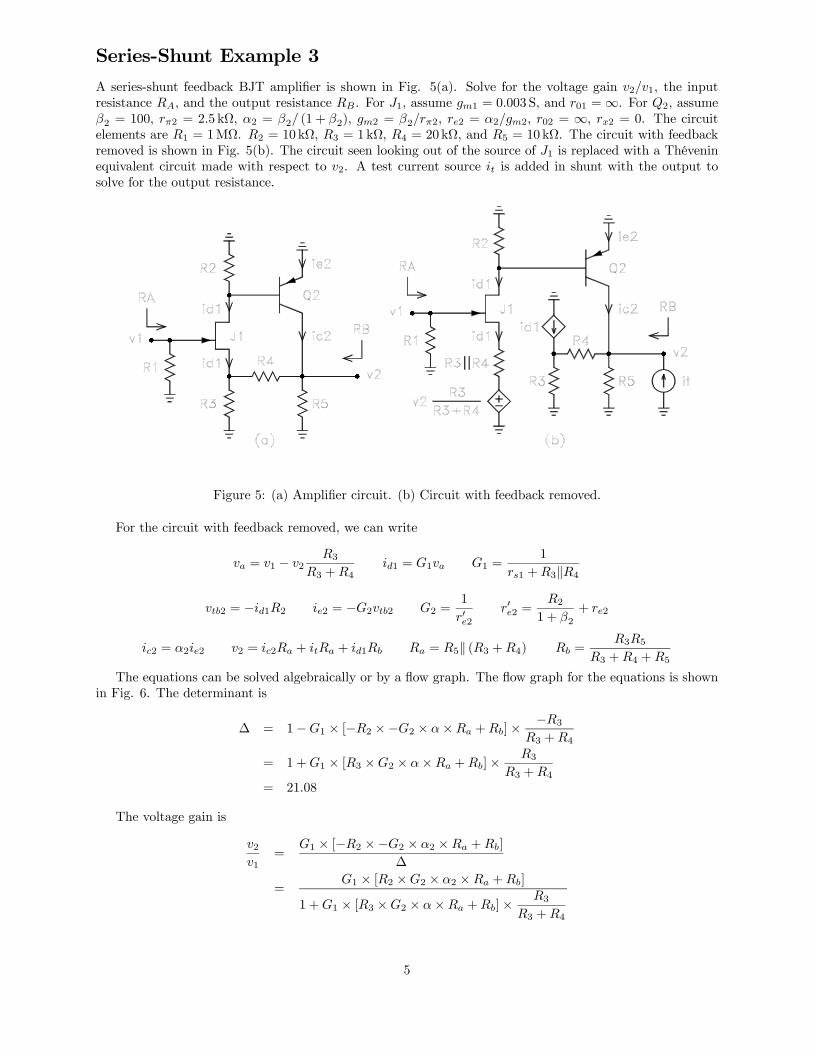
Series-Shunt Example 3A series-shunt feedback BJT amplifier is shown in Fig. 5(a). Solve for the voltage gain v2/v1, the inputresistance RA, and the output resistance RB . For J1, assume gm1 = 0.003 S, and r01 =∞. For Q2, assumeβ2 = 100, rπ2 = 2.5 kΩ, α2 = β2/ (1 + β2), gm2 = β2/rπ2, re2 = α2/gm2, r02 = ∞, rx2 = 0. The circuitelements are R1 = 1MΩ. R2 = 10 kΩ, R3 = 1kΩ, R4 = 20kΩ, and R5 = 10 kΩ. The circuit with feedbackremoved is shown in Fig. 5(b). The circuit seen looking out of the source of J1 is replaced with a Théveninequivalent circuit made with respect to v2. A test current source it is added in shunt with the output tosolve for the output resistance.
Figure 5: (a) Amplifier circuit. (b) Circuit with feedback removed.
For the circuit with feedback removed, we can write
va = v1 − v2R3
R3 +R4id1 = G1va G1 =
1
rs1 +R3kR4
vtb2 = −id1R2 ie2 = −G2vtb2 G2 =1
r0e2r0e2 =
R21 + β2
+ re2
ic2 = α2ie2 v2 = ic2Ra + itRa + id1Rb Ra = R5k (R3 +R4) Rb =R3R5
R3 +R4 +R5
The equations can be solved algebraically or by a flow graph. The flow graph for the equations is shownin Fig. 6. The determinant is
∆ = 1−G1 × [−R2 ×−G2 × α×Ra +Rb]× −R3R3 +R4
= 1 +G1 × [R3 ×G2 × α×Ra +Rb]× R3R3 +R4
= 21.08
The voltage gain is
v2v1
=G1 × [−R2 ×−G2 × α2 ×Ra +Rb]
∆
=G1 × [R2 ×G2 × α2 ×Ra +Rb]
1 +G1 × [R3 ×G2 × α×Ra +Rb]× R3R3 +R4
5
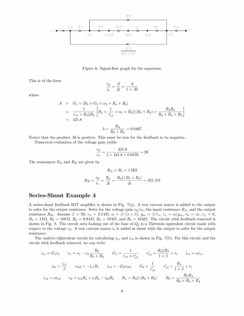
Figure 6: Signal-flow graph for the equations.
This is of the formv2i1=
A
∆=
A
1 +Ab
where
A = G1 × [R2 ×G2 × α2 ×Ra +Rb]
=1
rs1 +R3kR4
·R2 × 1
r0e1× α1 ×R5k (R3 +R4) +
R3R4R3 +R4 +R5
¸= 421.8
b =R3
R3 +R4= 0.0467
Notice that the product Ab is positive. This must be true for the feedback to be negative.Numerical evaluation of the voltage gain yields
v2v1=
421.8
1 + 421.8× 0.0476 = 20
The resistances RA and RB are given by
RA = R1 = 1MΩ
RB =v2it=
Ra
∆=
R5k (R3 +R4)
∆= 321.3Ω
Series-Shunt Example 4A series-shunt feedback BJT amplifier is shown in Fig. 7(a). A test current source is added to the outputto solve for the output resistance. Solve for the voltage gain v2/v1, the input resistance RA, and the outputresistance RB . Assume β = 50, rπ = 2.5 kΩ, α = β/ (1 + β), gm = β/rπ, re = α/gm, r0 = ∞, rx = 0,R1 = 1kΩ, R2 = 100Ω, R3 = 9.9 kΩ, R4 = 10 kΩ, and R5 = 10 kΩ. The circuit with feedback removed isshown in Fig. 8. The circuit seen looking out of the base of Q2 is a Thévenin equivalent circuit made withrespect to the voltage v2. A test current source it is added in shunt with the output to solve for the outputresistance.The emitter eQuivalent circuit for calculating ie1 and ie2 is shown in Fig. 7(b). For this circuit and the
circuit with feedback removed, we can write
ie1 = G1ve ve = v1 − v2R2
R2 +R3G1 =
1
re1 + r0e2r0e2 =
R2kR31 + β
+ re ic1 = αie1
ib1 =ic1β
vtb3 = −ic1R1 ie3 = −G2vtb3 G2 =1
r0e3r0e3 =
R11 + β
+ re
ic3 = αie3 v2 = ic3Ra + itRa − ib2Rb Ra = R4k (R2 +R3) Rb =R2R4
R2 +R3 +R4
6
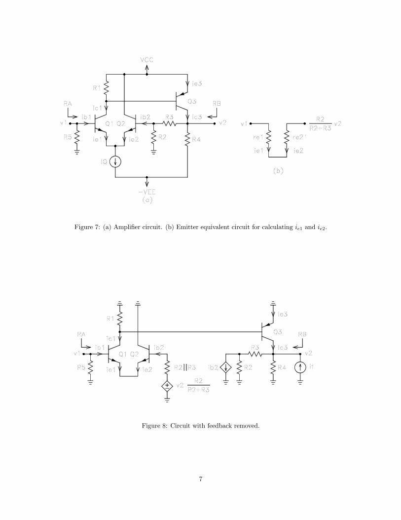
Figure 7: (a) Amplifier circuit. (b) Emitter equivalent circuit for calculating ie1 and ie2.
Figure 8: Circuit with feedback removed.
7
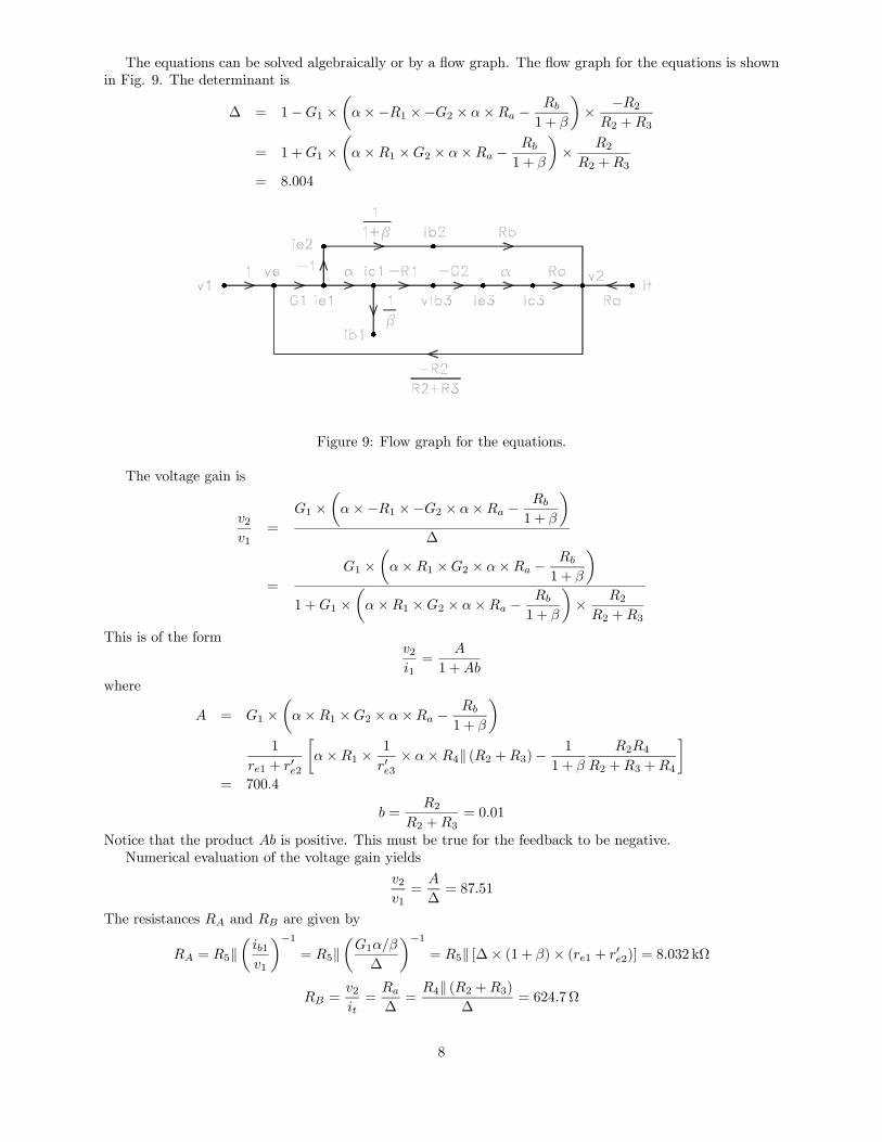
The equations can be solved algebraically or by a flow graph. The flow graph for the equations is shownin Fig. 9. The determinant is
∆ = 1−G1 ×µα×−R1 ×−G2 × α×Ra − Rb
1 + β
¶× −R2
R2 +R3
= 1 +G1 ×µα×R1 ×G2 × α×Ra − Rb
1 + β
¶× R2
R2 +R3= 8.004
Figure 9: Flow graph for the equations.
The voltage gain is
v2v1
=
G1 ×µα×−R1 ×−G2 × α×Ra − Rb
1 + β
¶∆
=
G1 ×µα×R1 ×G2 × α×Ra − Rb
1 + β
¶1 +G1 ×
µα×R1 ×G2 × α×Ra − Rb
1 + β
¶× R2
R2 +R3
This is of the formv2i1=
A
1 +Abwhere
A = G1 ×µα×R1 ×G2 × α×Ra − Rb
1 + β
¶1
re1 + r0e2
·α×R1 × 1
r0e3× α×R4k (R2 +R3)− 1
1 + β
R2R4R2 +R3 +R4
¸= 700.4
b =R2
R2 +R3= 0.01
Notice that the product Ab is positive. This must be true for the feedback to be negative.Numerical evaluation of the voltage gain yields
v2v1=
A
∆= 87.51
The resistances RA and RB are given by
RA = R5kµib1v1
¶−1= R5k
µG1α/β
∆
¶−1= R5k [∆× (1 + β)× (re1 + r0e2)] = 8.032 kΩ
RB =v2it=
Ra
∆=
R4k (R2 +R3)
∆= 624.7Ω
8
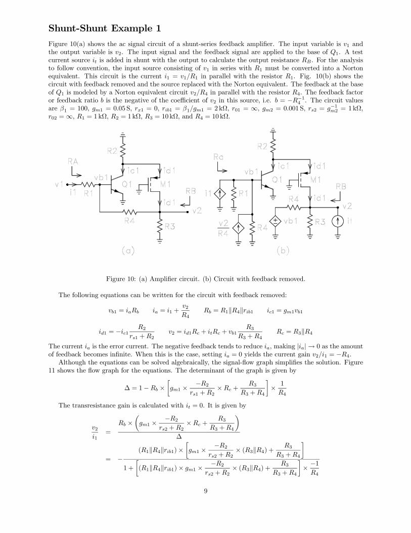
Shunt-Shunt Example 1Figure 10(a) shows the ac signal circuit of a shunt-series feedback amplifier. The input variable is v1 andthe output variable is v2. The input signal and the feedback signal are applied to the base of Q1. A testcurrent source it is added in shunt with the output to calculate the output resistance RB. For the analysisto follow convention, the input source consisting of v1 in series with R1 must be converted into a Nortonequivalent. This circuit is the current i1 = v1/R1 in parallel with the resistor R1. Fig. 10(b) shows thecircuit with feedback removed and the source replaced with the Norton equivalent. The feedback at the baseof Q1 is modeled by a Norton equivalent circuit v2/R4 in parallel with the resistor R4. The feedback factoror feedback ratio b is the negative of the coefficient of v2 in this source, i.e. b = −R−14 . The circuit valuesare β1 = 100, gm1 = 0.05 S, rx1 = 0, rib1 = β1/gm1 = 2kΩ, r01 = ∞, gm2 = 0.001 S, rs2 = g−1m2 = 1kΩ,r02 =∞, R1 = 1kΩ, R2 = 1kΩ, R3 = 10kΩ, and R4 = 10 kΩ.
Figure 10: (a) Amplifier circuit. (b) Circuit with feedback removed.
The following equations can be written for the circuit with feedback removed:
vb1 = iaRb ia = i1 +v2R4
Rb = R1kR4krib1 ic1 = gm1vb1
id1 = −ic1 R2rs1 +R2
v2 = id1Rc + itRc + vb1R3
R3 +R4Rc = R3kR4
The current ia is the error current. The negative feedback tends to reduce ia, making |ia|→ 0 as the amountof feedback becomes infinite. When this is the case, setting ia = 0 yields the current gain v2/i1 = −R4.Although the equations can be solved algebraically, the signal-flow graph simplifies the solution. Figure
11 shows the flow graph for the equations. The determinant of the graph is given by
∆ = 1−Rb ×·gm1 × −R2
rs1 +R2×Rc +
R3R3 +R4
¸× 1
R4
The transresistance gain is calculated with it = 0. It is given by
v2i1
=
Rb ×µgm1 × −R2
rs2 +R2×Rc +
R3R3 +R4
¶∆
= −(R1kR4krib1)×
·gm1 × −R2
rs2 +R2× (R3kR4) + R3
R3 +R4
¸1 +
·(R1kR4krib1)× gm1 × −R2
rs2 +R2× (R3kR4) + R3
R3 +R4
¸× −1
R4
9
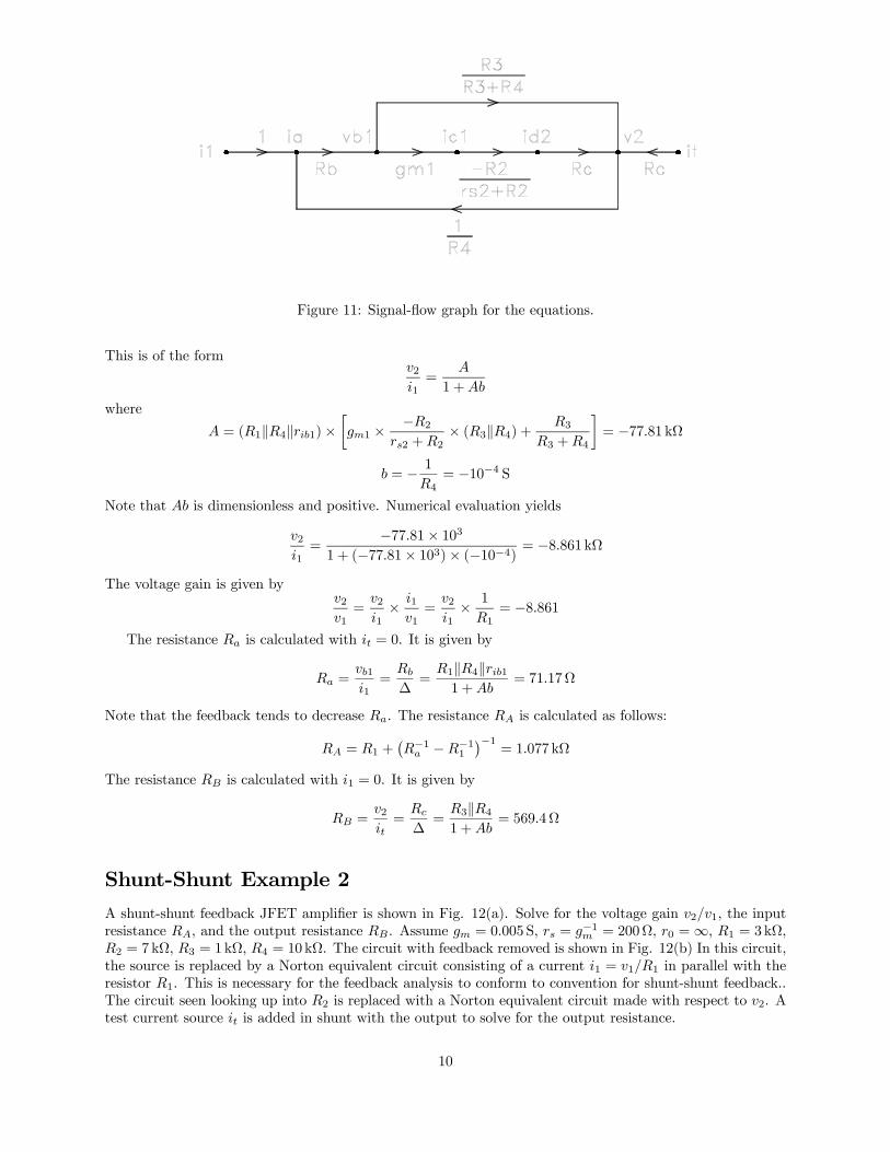
Figure 11: Signal-flow graph for the equations.
This is of the formv2i1=
A
1 +Ab
where
A = (R1kR4krib1)×·gm1 × −R2
rs2 +R2× (R3kR4) + R3
R3 +R4
¸= −77.81 kΩ
b = − 1
R4= −10−4 S
Note that Ab is dimensionless and positive. Numerical evaluation yields
v2i1=
−77.81× 1031 + (−77.81× 10³)× (−10−4) = −8.861 kΩ
The voltage gain is given byv2v1=
v2i1× i1
v1=
v2i1× 1
R1= −8.861
The resistance Ra is calculated with it = 0. It is given by
Ra =vb1i1=
Rb
∆=
R1kR4krib11 +Ab
= 71.17Ω
Note that the feedback tends to decrease Ra. The resistance RA is calculated as follows:
RA = R1 +¡R−1a −R−11
¢−1= 1.077 kΩ
The resistance RB is calculated with i1 = 0. It is given by
RB =v2it=
Rc
∆=
R3kR41 +Ab
= 569.4Ω
Shunt-Shunt Example 2A shunt-shunt feedback JFET amplifier is shown in Fig. 12(a). Solve for the voltage gain v2/v1, the inputresistance RA, and the output resistance RB . Assume gm = 0.005 S, rs = g−1m = 200Ω, r0 =∞, R1 = 3kΩ,R2 = 7kΩ, R3 = 1kΩ, R4 = 10kΩ. The circuit with feedback removed is shown in Fig. 12(b) In this circuit,the source is replaced by a Norton equivalent circuit consisting of a current i1 = v1/R1 in parallel with theresistor R1. This is necessary for the feedback analysis to conform to convention for shunt-shunt feedback..The circuit seen looking up into R2 is replaced with a Norton equivalent circuit made with respect to v2. Atest current source it is added in shunt with the output to solve for the output resistance.
10
Figure 12: (a) Amplifier circuit. (b) Circuit with feedback removed.
For the circuit with feedback removed, we can write
vg = i1Rb +v2R2
Rb Rb = R1kR2 id = Gmvg Gm =1
rs +R3
v2 = −idRc + itRc + vgR4
R2 +R4Rc = R2kR4
The equations can be solved algebraically or by a flow graph. The flow graph for the equations is shownin Fig. 13. The determinant is
∆ = 1−Rb ×·Gm ×−Rc +
R4R2 +R4
¸× 1
R2
= 1 +Rb ×·Gm ×Rc − R4
R2 +R4
¸× 1
R2= 1.853Ω
Figure 13: Signal-flow graph for the equations.
11
The transresistance gain is
v2i1
=
Rb ×·Gm ×−Rc +
R4R2 +R4
¸∆
=
−Rb ×·Gm ×Rc − R4
R2 +R4
¸1 +Rb ×
·Gm ×Rc +
R4R2 +R4
¸× 1
R2
This is of the formv2i1=
A
1 +Ab
where
A = −Rb ×·Gm ×Rc − R4
R2 +R4
¸= − (R1kR2)×
·Gm ×R2kR4 − R4
R2 +R4
¸= −5.971 kΩ
b = − 1
R2= −0.1429mS
Note that the product Ab is dimensionless and positive. The latter must be true for the feedback to benegative. Numerical evaluation yields
v2i1=
A
∆= −3.22 kΩ
The voltage gain is given by
v2v1=
v2i1× i1
v1=
A
∆× 1
R1= −1.074
The resistances Ra, RA, and RB are given by
Ra =vgi1=
Rb
∆= 1.13 kΩ
RA = R1 +
µ1
Ra− 1
R1
¶−1= 4.82 kΩ
RB =v2it=
Rc
∆= 2.22 kΩ
Shunt-Shunt Example 3A shunt-shunt feedback BJT amplifier is shown in Fig. 14. The input variable is the v1 and the outputvariable is the voltage v2. The feedback resistor is R2. The summing at the input is shunt because theinput through R1 and the feedback through R2 connect in shunt to the same node, i.e. the vb1 node. Theoutput sampling is shunt because R2 connects to the output node. Solve for the voltage gain v2/v1, the inputresistance RA, and the output resistance RB. Assume β = 100, rπ = 2.5 kΩ, gm = β/rπ, α = β/ (1 + β),re = α/gm, r0 = ∞, rx = 0, VT = 25mV. The resistor values are R1 = 1kΩ, R2 = 20 kΩ, R3 = 500Ω,R4 = 1kΩ, and R5 = 5kΩ.The circuit with feedback removed is shown in Fig. 15. A test current source it is added in shunt with
the output to solve for the output resistance RB. In the circuit, the source is replaced by a Norton equivalentcircuit consisting of a current
i1 =v1R1
12
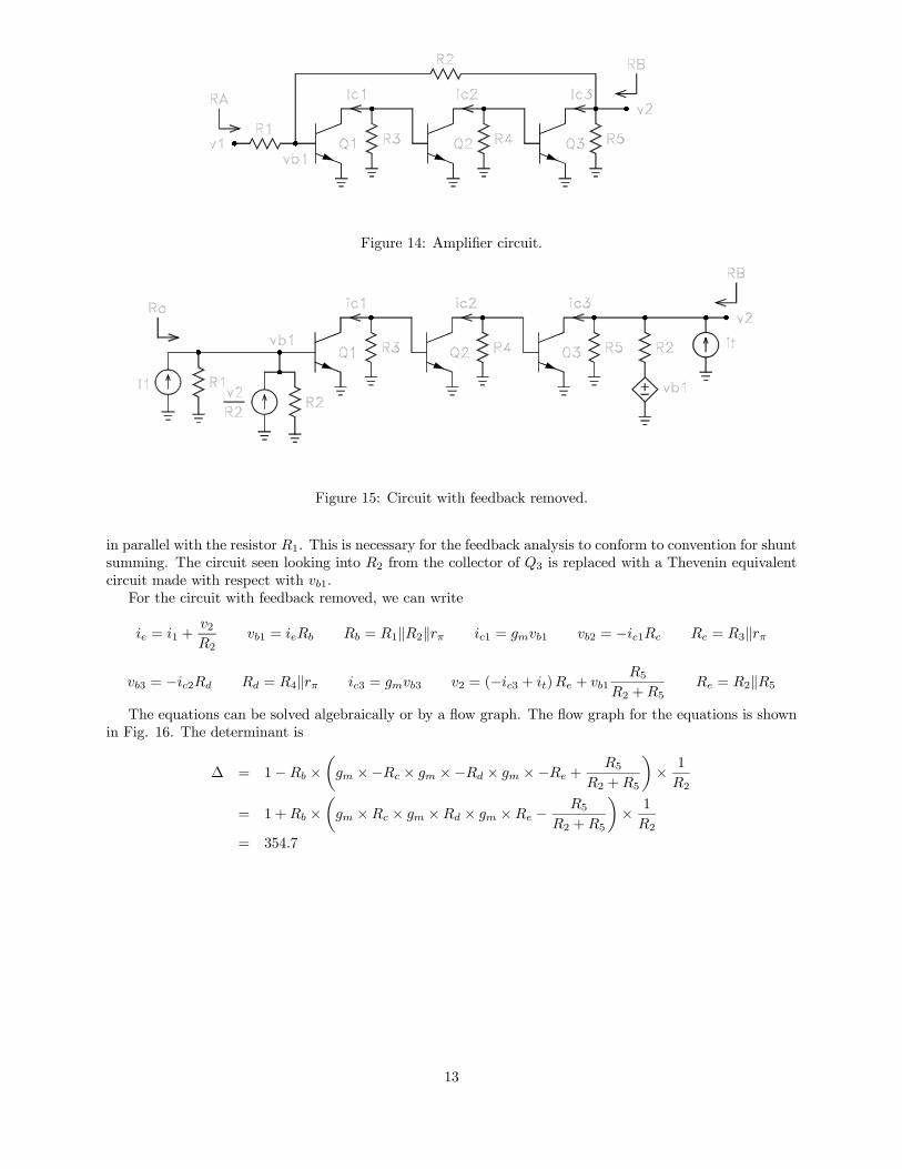
Figure 14: Amplifier circuit.
Figure 15: Circuit with feedback removed.
in parallel with the resistor R1. This is necessary for the feedback analysis to conform to convention for shuntsumming. The circuit seen looking into R2 from the collector of Q3 is replaced with a Thevenin equivalentcircuit made with respect with vb1.For the circuit with feedback removed, we can write
ie = i1 +v2R2
vb1 = ieRb Rb = R1kR2krπ ic1 = gmvb1 vb2 = −ic1Rc Rc = R3krπ
vb3 = −ic2Rd Rd = R4krπ ic3 = gmvb3 v2 = (−ic3 + it)Re + vb1R5
R2 +R5Re = R2kR5
The equations can be solved algebraically or by a flow graph. The flow graph for the equations is shownin Fig. 16. The determinant is
∆ = 1−Rb ×µgm ×−Rc × gm ×−Rd × gm ×−Re +
R5R2 +R5
¶× 1
R2
= 1 +Rb ×µgm ×Rc × gm ×Rd × gm ×Re − R5
R2 +R5
¶× 1
R2= 354.7
13
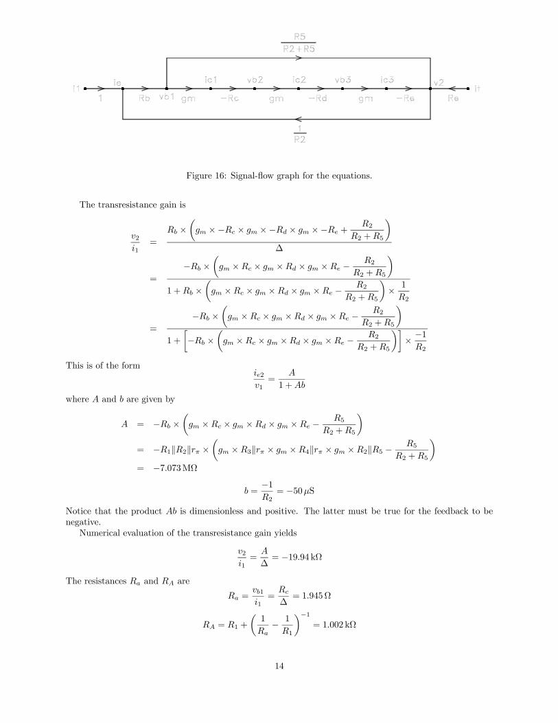
Figure 16: Signal-flow graph for the equations.
The transresistance gain is
v2i1
=
Rb ×µgm ×−Rc × gm ×−Rd × gm ×−Re +
R2R2 +R5
¶∆
=
−Rb ×µgm ×Rc × gm ×Rd × gm ×Re − R2
R2 +R5
¶1 +Rb ×
µgm ×Rc × gm ×Rd × gm ×Re − R2
R2 +R5
¶× 1
R2
=
−Rb ×µgm ×Rc × gm ×Rd × gm ×Re − R2
R2 +R5
¶1 +
·−Rb ×
µgm ×Rc × gm ×Rd × gm ×Re − R2
R2 +R5
¶¸× −1
R2
This is of the formie2v1=
A
1 +Ab
where A and b are given by
A = −Rb ×µgm ×Rc × gm ×Rd × gm ×Re − R5
R2 +R5
¶= −R1kR2krπ ×
µgm ×R3krπ × gm ×R4krπ × gm ×R2kR5 − R5
R2 +R5
¶= −7.073MΩ
b =−1R2
= −50µS
Notice that the product Ab is dimensionless and positive. The latter must be true for the feedback to benegative.Numerical evaluation of the transresistance gain yields
v2i1=
A
∆= −19.94 kΩ
The resistances Ra and RA are
Ra =vb1i1=
Rc
∆= 1.945Ω
RA = R1 +
µ1
Ra− 1
R1
¶−1= 1.002 kΩ
14
The resistance RB is
RB =v2it=
Re
∆= 11.28Ω
The voltage gain isv2vb1
=v2i1×µvb1i1
¶−1=
µA
∆
¶× 1
RA= −19.91
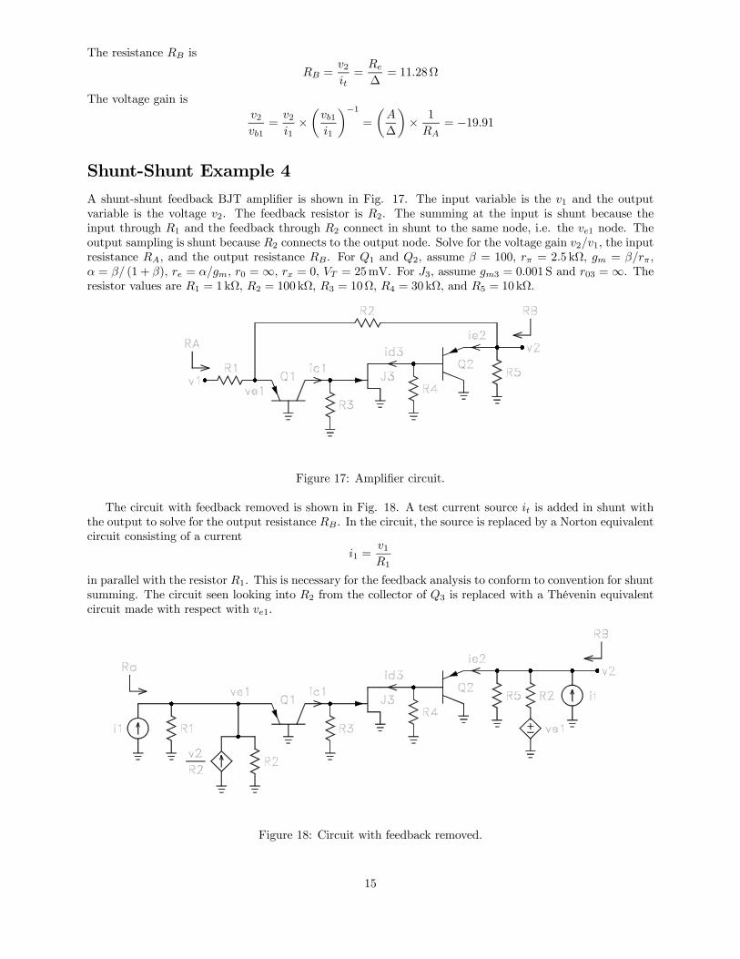
Shunt-Shunt Example 4A shunt-shunt feedback BJT amplifier is shown in Fig. 17. The input variable is the v1 and the outputvariable is the voltage v2. The feedback resistor is R2. The summing at the input is shunt because theinput through R1 and the feedback through R2 connect in shunt to the same node, i.e. the ve1 node. Theoutput sampling is shunt because R2 connects to the output node. Solve for the voltage gain v2/v1, the inputresistance RA, and the output resistance RB. For Q1 and Q2, assume β = 100, rπ = 2.5 kΩ, gm = β/rπ,α = β/ (1 + β), re = α/gm, r0 =∞, rx = 0, VT = 25mV. For J3, assume gm3 = 0.001 S and r03 =∞. Theresistor values are R1 = 1kΩ, R2 = 100 kΩ, R3 = 10Ω, R4 = 30kΩ, and R5 = 10 kΩ.
Figure 17: Amplifier circuit.
The circuit with feedback removed is shown in Fig. 18. A test current source it is added in shunt withthe output to solve for the output resistance RB. In the circuit, the source is replaced by a Norton equivalentcircuit consisting of a current
i1 =v1R1
in parallel with the resistor R1. This is necessary for the feedback analysis to conform to convention for shuntsumming. The circuit seen looking into R2 from the collector of Q3 is replaced with a Thévenin equivalentcircuit made with respect with ve1.
Figure 18: Circuit with feedback removed.
15
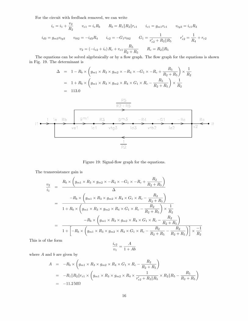
For the circuit with feedback removed, we can write
ie = i1 +v2R2
ve1 = ieRb Rb = R1kR2kre1 ic1 = gm1ve1 vtg3 = ic1R3
id3 = gm3vtg3 vtb2 = −id3R4 ie2 = −G1vtb2 G1 =1
r0e2 +R2kR5 r0e2 =1
R4+ re2
v2 = (−ie2 + it)Rc + ve1R5
R2 +R5Rc = R2kR5
The equations can be solved algebraically or by a flow graph. The flow graph for the equations is shownin Fig. 19. The determinant is
∆ = 1−Rb ×µgm1 ×R3 × gm2 ×−R4 ×−G1 ×−Rc +
R5R2 +R5
¶× 1
R2
= 1 +Rb ×µgm1 ×R3 × gm2 ×R4 ×G1 ×Rc − R5
R2 +R5
¶× 1
R2= 113.0
Figure 19: Signal-flow graph for the equations.
The transresistance gain is
v2i1
=
Rb ×µgm1 ×R3 × gm2 ×−R4 ×−G1 ×−Rc +
R2R2 +R5
¶∆
=
−Rb ×µgm1 ×R3 × gm2 ×R4 ×G1 ×Rc − R2
R2 +R5
¶1 +Rb ×
µgm1 ×R3 × gm2 ×R4 ×G1 ×Rc − R2
R2 +R5
¶× 1
R2
=
−Rb ×µgm1 ×R3 × gm2 ×R4 ×G1 ×Rc − R2
R2 +R5
¶1 +
·−Rb ×
µgm1 ×R3 × gm2 ×R4 ×G1 ×Rc − R2
R2 +R5− R2
R2 +R5
¶¸× −1
R2
This is of the formie2v1=
A
1 +Ab
where A and b are given by
A = −Rb ×µgm1 ×R3 × gm2 ×R4 ×G1 ×Rc − R2
R2 +R5
¶= −R1kR2kre1 ×
µgm1 ×R3 × gm2 ×R4 × 1
r0e2 +R2kR5 ×R2kR5 − R5R2 +R5
¶= −11.2MΩ
16
b =−1R2
= −10µS
Notice that the product Ab is dimensionless and positive. The latter must be true for the feedback to benegative.Numerical evaluation of the transresistance gain yields
v2i1=
A
∆= −99.11 kΩ
The resistances Ra and RA are
Ra =ve1i1=
Rb
∆= 0.214Ω
RA = R1 +
µ1
Ra− 1
R1
¶−1= 1kΩ
The resistance RB is
RB =v2it=
Rc
∆= 80.49Ω
The voltage gain isv2ve1
=v2i1×µve1i1
¶−1=
µA
∆
¶× 1
RA= −99.09
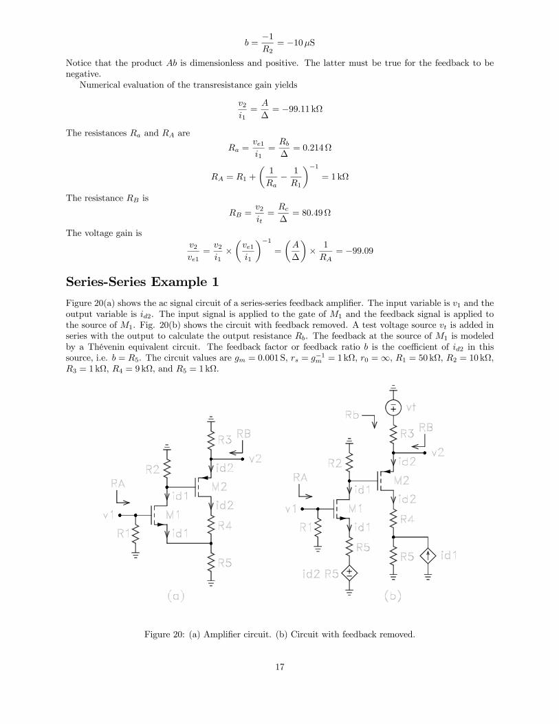
Series-Series Example 1Figure 20(a) shows the ac signal circuit of a series-series feedback amplifier. The input variable is v1 and theoutput variable is id2. The input signal is applied to the gate of M1 and the feedback signal is applied tothe source of M1. Fig. 20(b) shows the circuit with feedback removed. A test voltage source vt is added inseries with the output to calculate the output resistance Rb. The feedback at the source of M1 is modeledby a Thévenin equivalent circuit. The feedback factor or feedback ratio b is the coefficient of id2 in thissource, i.e. b = R5. The circuit values are gm = 0.001 S, rs = g−1m = 1kΩ, r0 =∞, R1 = 50 kΩ, R2 = 10kΩ,R3 = 1kΩ, R4 = 9kΩ, and R5 = 1kΩ.
Figure 20: (a) Amplifier circuit. (b) Circuit with feedback removed.
17
The following equations can be written for the circuit with feedback removed:
id1 = Gm1va Gm1 =1
rs1 +R5va = v1 − vts1 vts1 = id2R5
id2 = Gm2vb Gm2 =1
rs2 +R3vb = vt − vtg2 vtg2 = −id1R2
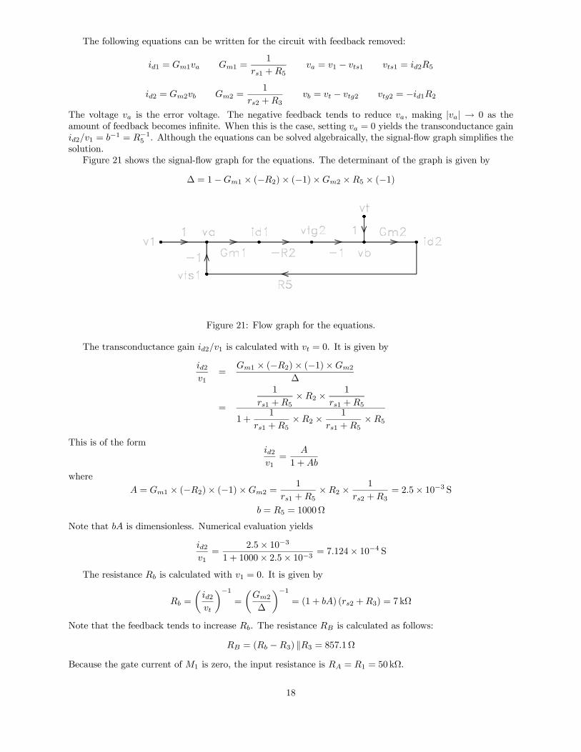
The voltage va is the error voltage. The negative feedback tends to reduce va, making |va| → 0 as theamount of feedback becomes infinite. When this is the case, setting va = 0 yields the transconductance gainid2/v1 = b−1 = R−15 . Although the equations can be solved algebraically, the signal-flow graph simplifies thesolution.Figure 21 shows the signal-flow graph for the equations. The determinant of the graph is given by
∆ = 1−Gm1 × (−R2)× (−1)×Gm2 ×R5 × (−1)
Figure 21: Flow graph for the equations.
The transconductance gain id2/v1 is calculated with vt = 0. It is given by
id2v1
=Gm1 × (−R2)× (−1)×Gm2
∆
=
1
rs1 +R5×R2 × 1
rs1 +R5
1 +1
rs1 +R5×R2 × 1
rs1 +R5×R5
This is of the formid2v1=
A
1 +Ab
whereA = Gm1 × (−R2)× (−1)×Gm2 =
1
rs1 +R5×R2 × 1
rs2 +R3= 2.5× 10⁻³ S
b = R5 = 1000Ω
Note that bA is dimensionless. Numerical evaluation yields
id2v1=
2.5× 10⁻³¹ + 1000× 2.5× 10−3 = 7.124× 10
−4 S
The resistance Rb is calculated with v1 = 0. It is given by
Rb =
µid2vt
¶−1=
µGm2
∆
¶−1= (1 + bA) (rs2 +R3) = 7 kΩ
Note that the feedback tends to increase Rb. The resistance RB is calculated as follows:
RB = (Rb −R3) kR3 = 857.1ΩBecause the gate current of M1 is zero, the input resistance is RA = R1 = 50 kΩ.
18
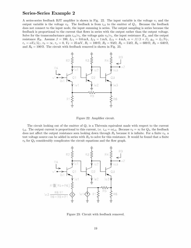
Series-Series Example 2A series-series feedback BJT amplifier is shown in Fig. 22. The input variable is the voltage v1 and theoutput variable is the voltage v2. The feedback is from ie2 to the emitter of Q1. Because the feedbackdoes not connect to the input node, the input summing is series. The output sampling is series because thefeedback is proportional to the current that flows in series with the output rather than the output voltage.Solve for the transconductance gain ic3/v1, the voltage gain v2/v1, the input resistance RA, and the outputresistance RB. Assume β = 100, IC1 = 0.6mA, IC2 = 1mA, IC3 = 4mA, α = β/ (1 + β), gm = IC/VT ,re = αVT /IC , r0 = ∞, rx = 0, VT = 25mV, R1 = 100Ω, R2 = 9kΩ, R3 = 5kΩ, R4 = 600Ω, R5 = 640Ω,and R6 = 100Ω. The circuit with feedback removed is shown in Fig. 23.
Figure 22: Amplifier circuit.
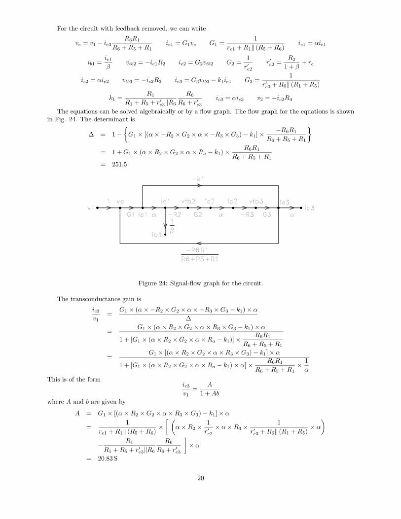
The circuit looking out of the emitter of Q1 is a Thévenin equivalent made with respect to the currentie3. The output current is proportional to this current, i.e. ic3 = αie3. Because r0 =∞ for Q3, the feedbackdoes not affect the output resistance seen looking down through R4 because it is infinite. For a finite r0, atest voltage source can be added in series with R4 to solve for this resistance. It would be found that a finiter0 for Q3 considerably complicates the circuit equations and the flow graph.
Figure 23: Circuit with feedback removed.
19
For the circuit with feedback removed, we can write
ve = v1 − ie3R6R1
R6 +R5 +R1ie1 = G1ve G1 =
1
re1 +R1k (R5 +R6)ic1 = αie1
ib1 =ic1β
vtb2 = −ic1R2 ie2 = G2vtb2 G2 =1
r0e2r0e2 =
R21 + β
+ re
ic2 = αie2 vtb3 = −ic2R3 ie3 = G3vtb3 − k1ie1 G3 =1
r0e3 +R6k (R1 +R5)
k1 =R1
R1 +R5 + r0e3kR6R6
R6 + r0e3ic3 = αie3 v2 = −ic2R4
The equations can be solved algebraically or by a flow graph. The flow graph for the equations is shownin Fig. 24. The determinant is
∆ = 1−½G1 × [(α×−R2 ×G2 × α×−R3 ×G3)− k1]× −R6R1
R6 +R5 +R1
¾= 1 +G1 × (α×R2 ×G2 × α×Ra − k1)× R6R1
R6 +R5 +R1= 251.5
Figure 24: Signal-flow graph for the circuit.
The transconductance gain is
ic3v1
=G1 × (α×−R2 ×G2 × α×−R3 ×G3 − k1)× α
∆
=G1 × (α×R2 ×G2 × α×R3 ×G3 − k1)× α
1 + [G1 × (α×R2 ×G2 × α×Ra − k1)]× R6R1R6 +R5 +R1
=G1 × [(α×R2 ×G2 × α×R3 ×G3)− k1]× α
1 + [G1 × (α×R2 ×G2 × α×Ra − k1)× α]× R6R1R6 +R5 +R1
× 1
α
This is of the formic3v1=
A
1 +Ab
where A and b are given by
A = G1 × [(α×R2 ×G2 × α×R3 ×G3)− k1]× α
=1
re1 +R1k (R5 +R6)×· µ
α×R2 × 1
r0e2× α×R3 × 1
r0e3 +R6k (R1 +R5)× α
¶− R1R1 +R5 + r0e3kR6
R6R6 + r0e3
¸× α
= 20.83 S
20
b =R6R1
R6 +R5 +R1× 1
α= 12.02Ω
Notice that the product Ab is dimensionless and positive. The latter must be true for the feedback to benegative.Numerical evaluation of the transconductance gain yields
ic3v1=
A
∆= 0.083
The voltage gain is given byv2v1=
ic3v1× v2
ic3=
A
∆×−R4 = −49.7
The resistances RA and RB are given by
RA =
µib1v1
¶−1=
µG1α/β
∆
¶−1=∆× (1 + β)
G1= ∆× (1 + β)× [re1 +R1k (R5 +R6)] = 3.285MΩ
RB = R4 = 600Ω
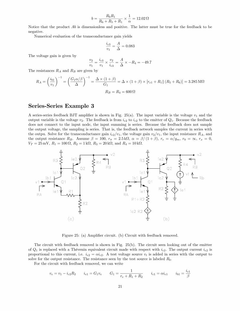
Series-Series Example 3A series-series feedback BJT amplifier is shown in Fig. 25(a). The input variable is the voltage v1 and theoutput variable is the voltage v2. The feedback is from ie2 to ic2 to the emitter of Q1. Because the feedbackdoes not connect to the input node, the input summing is series. Because the feedback does not samplethe output voltage, the sampling is series. That is, the feedback network samples the current in series withthe outpu. Solve for the transconductance gain ie2/v1, the voltage gain v2/v1, the input resistance RA, andthe output resistance RB. Assume β = 100, rπ = 2.5 kΩ, α = β/ (1 + β), re = α/gm, r0 = ∞, rx = 0,VT = 25mV, R1 = 100Ω, R2 = 1kΩ, R3 = 20 kΩ, and R4 = 10 kΩ.
Figure 25: (a) Amplifier circuit. (b) Circuit with feedback removed.
The circuit with feedback removed is shown in Fig. 25(b). The circuit seen looking out of the emitterof Q1 is replaced with a Thévenin equivalent circuit made with respect with ic2. The output current ie2 isproportional to this current, i.e. ie2 = αic2. A test voltage source vt is added in series with the output tosolve for the output resistance. The resistance seen by the test source is labeled Rb.For the circuit with feedback removed, we can write
ve = v1 − ic2R2 ie1 = G1ve G1 =1
re +R1 +R2ic1 = αie1 ib1 =
ic1β
21
vtb2 = −ic1R3 ie2 = G2 (vt − vtb2) G2 =1
r0e2 +R4r0e2 =
R31 + β
+ re ic2 = αie2
The equations can be solved algebraically or by a flow graph. The flow graph for the equations is shownin Fig. 26. The determinant is
∆ = 1− (G1 × α×−R3 ×−G2 × α×−R2)= 1 +G1 × α×R2 ×G2 × α×R2
= 1.181
Figure 26: Signal-flow graph for the equations.
The transconductance gain is
ie2v1
=G1 × α×−R3 ×−G2
∆
=(G1 × α×R3 ×G2)
1 + (G1 × α×R3 ×G2)× α×R2
This is of the formie2v1=
A
1 +Ab
where A and b are given by
A = G1 × α×R3 ×G2
=1
re1 +R1 +R2× α×R3 × 1
r0e2 +R4= 0.9117mS
b = αR2 = 1.98 kΩ
Notice that the product Ab is dimensionless and positive. The latter must be true for the feedback to benegative.Numerical evaluation of the transconductance gain yields
ie2v1=
A
∆= 0.325mS
The voltage gain is given byv2v1=
ie2v1× v2
ie2=
A
∆×−R4 = −3.25
The resistances RA and RB are given by
RA =
µib1v1
¶−1=
µG1α/β
∆
¶−1= ∆× (1 + β) (re +R1 +R2) = 602 kΩ
Rb =
µie2vt
¶−1=
µGm2
∆
¶−1= ∆× (R4 + r0e2) = 28.68 kΩ
RB = (Rb −R4) kR4 = 6.513 kΩ
22
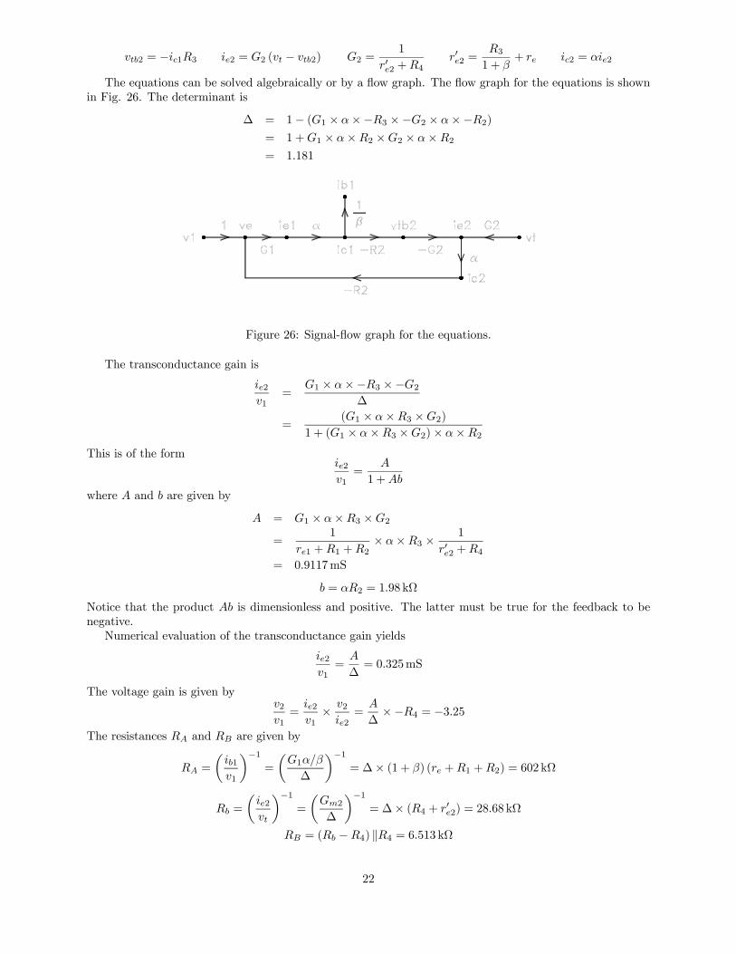
Series-Series Example 4A series-series feedback BJT amplifier is shown in Fig. 27(a). The input variable is the voltage v1 and theoutput variable is the current ic2. The feedback is from ic2 to ie2 to the gate of J1. The input summing isseries because the feedback does not connect to the same node that the source connects. The output samplingis series because the feedback is proportional to the output current ic2. Solve for the transconductance gainic2/v1, the voltage gain v2/v1, the input resistance RA, and the output resistance RB. For J1, assume thatgm1 = 0.001 S, rs1 = g−1m1 = 1000Ω, and r01 =∞. For Q2, assume β2 = 100, rπ2 = 2.5 kΩ, α2 = β2/ (1 + β2),re2 = α2/gm2, r02 = ∞, rx2 = 0, VT = 25mV. The resistor values are R1 = 1kΩ, R2 = 10 kΩ, R3 = 1kΩ,R4 = 10 kΩ, R5 = 1kΩ, and R6 = 10 kΩ.
Figure 27: (a) Amplifier circuit. (b) Circuit with feedback removed.
The circuit with feedback removed is shown in Fig. 27(b). The circuit seen looking out of the emitterof Q1 is replaced with a Thévenin equivalent circuit made with respect with ie2. The output current isproportional to this current, i.e. ic2 = α2ie2. Because r02 = ∞, the feedback does not affect the outputresistance seen looking down through R6 because it is infinite. For a finite r02, a test voltage source canbe added in series with R6 to solve for this resistance. It would be found that a finite r02 considerablycomplicates the circuit equations and the flow graph.For the circuit with feedback removed, we can write
id1 = gm1ve ve = ie2R5R3
R3 +R4 +R5− v1 vtb2 = −id1R2 ie2 = G1vtb2
G1 =1
r0e2 +R5k (R3 +R4)r0e2 =
R21 + β2
+ re2 ic2 = α2ie2
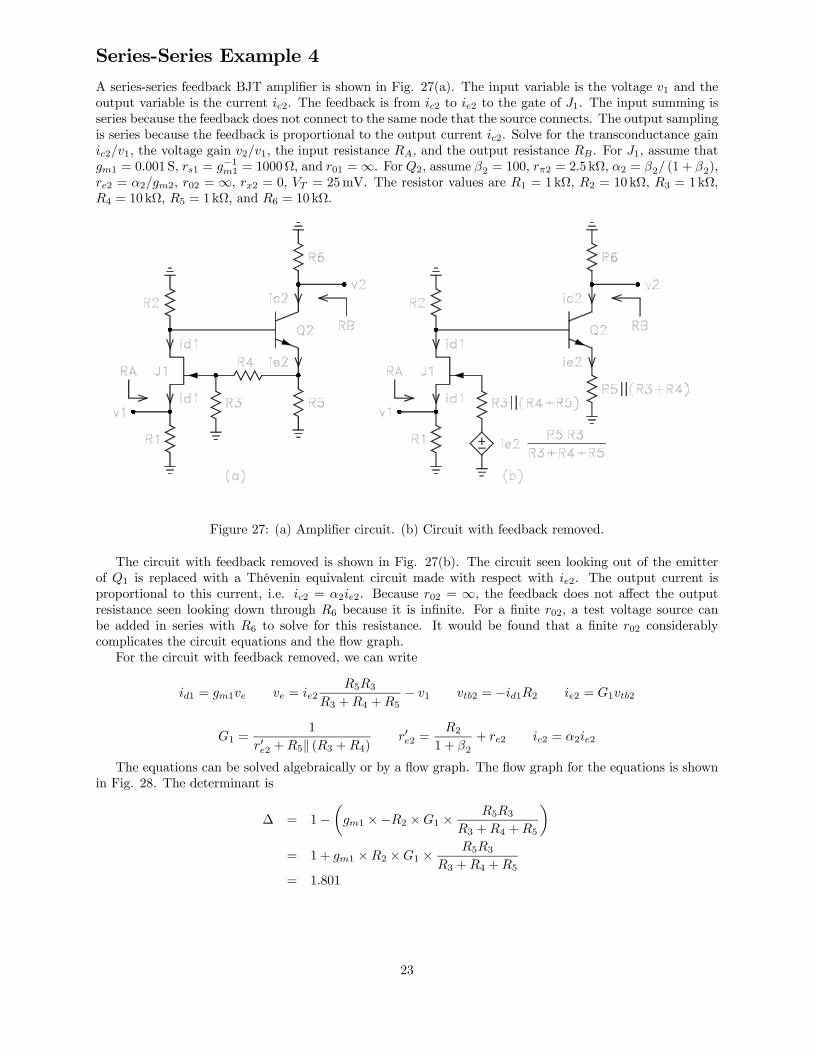
The equations can be solved algebraically or by a flow graph. The flow graph for the equations is shownin Fig. 28. The determinant is
∆ = 1−µgm1 ×−R2 ×G1 × R5R3
R3 +R4 +R5
¶= 1 + gm1 ×R2 ×G1 × R5R3
R3 +R4 +R5= 1.801
23
Figure 28: Signal-flow graph for the equations.
The transconductance gain is
ie2v1
=−1× gm1 ×−R2 ×G1 × α2
∆
=gm1 ×R2 ×G1 × α2
1 + gm1 ×R2 ×G1 × R5R3R3 +R4 +R5
=(gm1 ×R2 ×G1 × α2)
1 + (gm1 ×R2 ×G1 × α2)× R5R3R3 +R4 +R5
× 1
α2
This is of the formie2v1=
A
1 +Ab
where A and b are given by
A = gm1 ×R2 ×G1 × α2
= gm1 ×R2 × 1
r0e2 +R5k (R3 +R4)× α2
= 9.516mS
b =R5R3
R3 +R4 +R5× 1
α2= 84.17Ω
Notice that the product Ab is dimensionless and positive. The latter must be true for the feedback to benegative.Numerical evaluation of the transconductance gain yields
ic2v1=
A
∆= 5.284mS
The voltage gain is given byv2v1=
ic2v1× v2
ic2=
A
∆×−R6 = −52.84
The resistances RA and RB are given by
RA = R1kµ−id1
v1
¶−1= R1k
³gm1∆
´−1= R1k
µ∆
gm1
¶= 643Ω
RB = R6 = 10 kΩ
Series-Series Example 5A series-series feedback BJT amplifier is shown in Fig. 29. The input variable is the current i1 and theoutput variable is the current ie2. The feedback path is the path from ie2 to ic2 to ie3 to ic3 to the emitterof Q1. The input summing is series because the feedback does not connect to the input node. The output
24
sampling is series because the feedback is proportional to the output current ie2 and not the output voltagev2. Solve for the current gain gain ie2/i1, the transresistance gain v2/i1, the input resistance RA, and theoutput resistance RB. Assume β = 100, rπ = 2.5 kΩ, gm = β/rπ, α = β/ (1 + β), re = α/gm, r0 = ∞,rx = 0, VT = 25mV. The resistor values are R1 = 1kΩ, R2 = 100Ω, R3 = 10kΩ, R4 = 100Ω, R5 = 1kΩ,and R6 = 10kΩ.
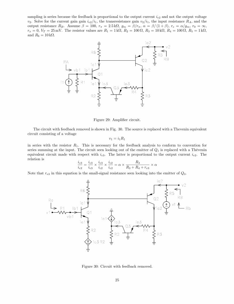
Figure 29: Amplifier circuit.
The circuit with feedback removed is shown in Fig. 30. The source is replaced with a Thevenin equivalentcircuit consisting of a voltage
v1 = i1R1
in series with the resistor R1. This is necessary for the feedback analysis to conform to convention forseries summing at the input. The circuit seen looking out of the emitter of Q1 is replaced with a Théveninequivalent circuit made with respect with ic3. The latter is proportional to the output current ie2. Therelation is
ic3ie2
=ic3ie3
× ie3ic2× ic2
ie2= α× R3
R3 +R4 + re3× α
Note that re3 in this equation is the small-signal resistance seen looking into the emitter of Q3.
Figure 30: Circuit with feedback removed.
25
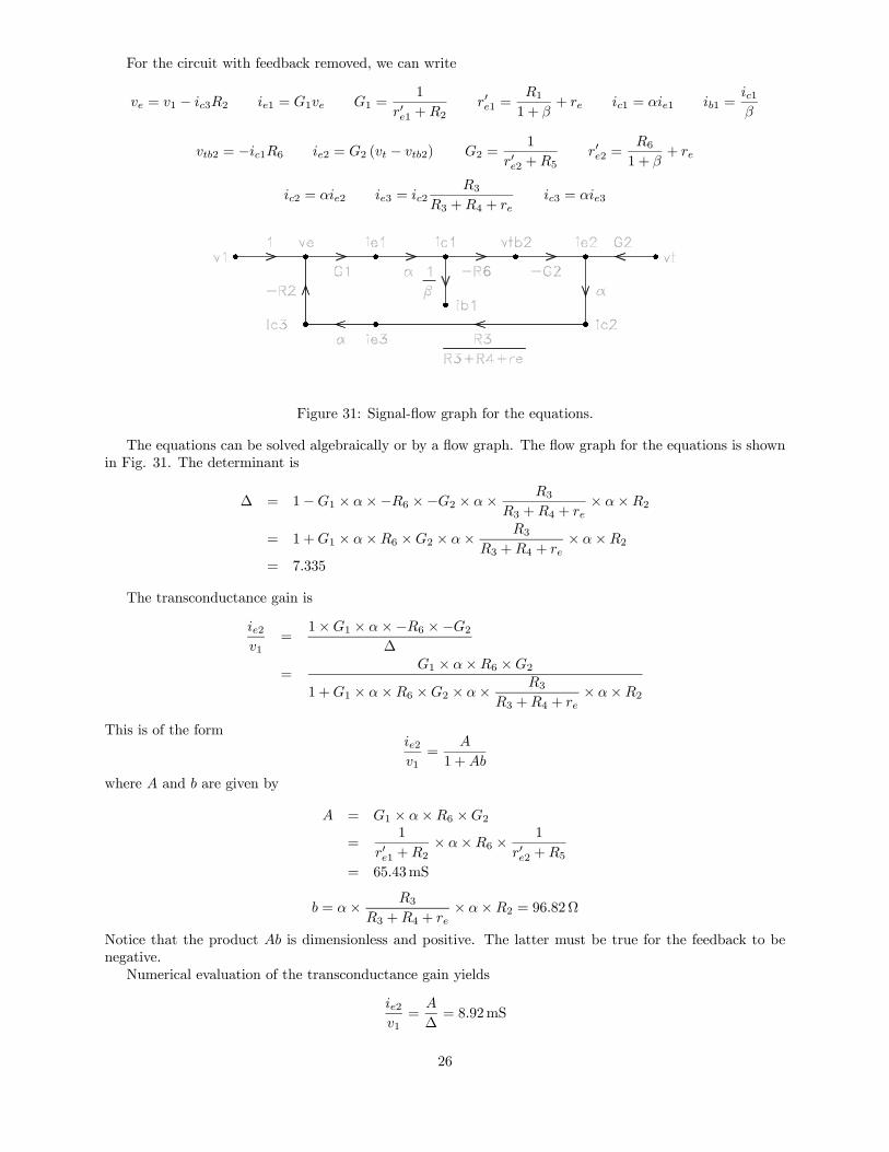
For the circuit with feedback removed, we can write
ve = v1 − ic3R2 ie1 = G1ve G1 =1
r0e1 +R2r0e1 =
R11 + β
+ re ic1 = αie1 ib1 =ic1β
vtb2 = −ic1R6 ie2 = G2 (vt − vtb2) G2 =1
r0e2 +R5r0e2 =
R61 + β
+ re
ic2 = αie2 ie3 = ic2R3
R3 +R4 + reic3 = αie3
Figure 31: Signal-flow graph for the equations.
The equations can be solved algebraically or by a flow graph. The flow graph for the equations is shownin Fig. 31. The determinant is
∆ = 1−G1 × α×−R6 ×−G2 × α× R3R3 +R4 + re
× α×R2
= 1 +G1 × α×R6 ×G2 × α× R3R3 +R4 + re
× α×R2
= 7.335
The transconductance gain is
ie2v1
=1×G1 × α×−R6 ×−G2
∆
=G1 × α×R6 ×G2
1 +G1 × α×R6 ×G2 × α× R3R3 +R4 + re
× α×R2
This is of the formie2v1=
A
1 +Ab
where A and b are given by
A = G1 × α×R6 ×G2
=1
r0e1 +R2× α×R6 × 1
r0e2 +R5= 65.43mS
b = α× R3R3 +R4 + re
× α×R2 = 96.82Ω
Notice that the product Ab is dimensionless and positive. The latter must be true for the feedback to benegative.Numerical evaluation of the transconductance gain yields
ie2v1=
A
∆= 8.92mS
26
The current gain is given byie2i1=
ie2v1× v1
i1=
A
∆×R1 = 8.92
The transresistance gain is
Rm =v2i1=
ie2i1× v2
ie2=
A
∆×R1 ×−R5 = −8.92 kΩ
The resistances Ra and RA
Ra =
µib1v1
¶−1=
µG1α/β
∆
¶−1= ∆× [R1 + rπ + (1 + β)R2] = 113.3 kΩ
RA =vb1i1= (Ra −R1) kR1 = 991.2Ω
The voltage gain isv2vb1
=v2i1×µvb1i1
¶−1=
µA
∆×R1
¶× 1
RA= −990
The resistances Rb and RB are
Rb =
µie2vt
¶−1=
µG2∆
¶−1= ∆× (r0e2 +R5) = 10.98 kΩ
RB = (Rb −R5) kR5 = 889.5Ω
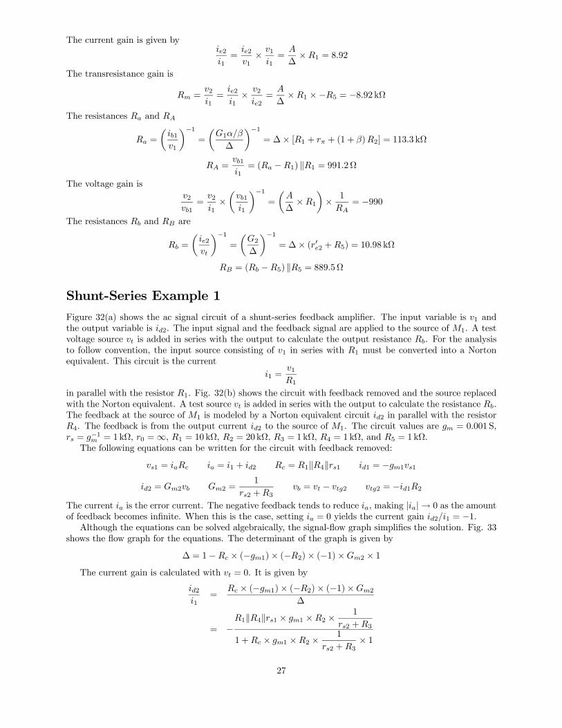
Shunt-Series Example 1Figure 32(a) shows the ac signal circuit of a shunt-series feedback amplifier. The input variable is v1 andthe output variable is id2. The input signal and the feedback signal are applied to the source of M1. A testvoltage source vt is added in series with the output to calculate the output resistance Rb. For the analysisto follow convention, the input source consisting of v1 in series with R1 must be converted into a Nortonequivalent. This circuit is the current
i1 =v1R1
in parallel with the resistor R1. Fig. 32(b) shows the circuit with feedback removed and the source replacedwith the Norton equivalent. A test source vt is added in series with the output to calculate the resistance Rb.The feedback at the source of M1 is modeled by a Norton equivalent circuit id2 in parallel with the resistorR4. The feedback is from the output current id2 to the source of M1. The circuit values are gm = 0.001 S,rs = g−1m = 1kΩ, r0 =∞, R1 = 10 kΩ, R2 = 20kΩ, R3 = 1kΩ, R4 = 1kΩ, and R5 = 1kΩ.The following equations can be written for the circuit with feedback removed:
vs1 = iaRc ia = i1 + id2 Rc = R1kR4krs1 id1 = −gm1vs1id2 = Gm2vb Gm2 =
1
rs2 +R3vb = vt − vtg2 vtg2 = −id1R2
The current ia is the error current. The negative feedback tends to reduce ia, making |ia|→ 0 as the amountof feedback becomes infinite. When this is the case, setting ia = 0 yields the current gain id2/i1 = −1.Although the equations can be solved algebraically, the signal-flow graph simplifies the solution. Fig. 33
shows the flow graph for the equations. The determinant of the graph is given by
∆ = 1−Rc × (−gm1)× (−R2)× (−1)×Gm2 × 1The current gain is calculated with vt = 0. It is given by
id2i1
=Rc × (−gm1)× (−R2)× (−1)×Gm2
∆
= −R1kR4krs1 × gm1 ×R2 × 1
rs2 +R3
1 +Rc × gm1 ×R2 × 1
rs2 +R3× 1
27
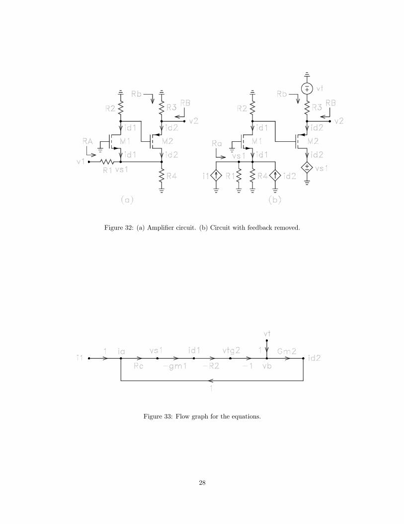
Figure 32: (a) Amplifier circuit. (b) Circuit with feedback removed.
Figure 33: Flow graph for the equations.
28
This is of the formid2i1=
A
1 +Ab
where
A = Rc × (−gm1)× (−R2)× (−1)×Gm2 = − (R1kR4krs1)× gm1 ×R2 × 1
rs2 +R3= −0.3333
b = −1Note that Ab is dimensionless. Numerical evaluation yields
id2i1=
2.5× 10⁻³¹ + 1000× 2.5× 10−3 = −0.7692
The voltage gain is given by
v2v1=
id2i1× i1
v1× v2
id2=
id2i1× 1
R1× (−R3) = 0.7692
The resistance Ra is calculated with vt = 0. It is given by
Ra =vs1i1=
Rc
∆=
R1kR4krs11 + 1×Rc × gm1 ×R2 × 1
rs2 +R3
= 76.92Ω
Note that the feedback tends to decrease Ra. The resistance RA is calculated as follows:
RA = R1 +¡R−1a −R−11
¢−1= 1.083 kΩ
The resistance Rb is calculated with i1 = 0. It is given by
Rb =
µid2vt
¶−1=
µGm2
∆
¶−1= (1 +Ab) (rs2 +R3) = 8.667 kΩ
Note that the feedback tends to increase Rb. The resistance RB is calculated as follows:
RB = (Rb −R3) kR3 = 884.6Ω
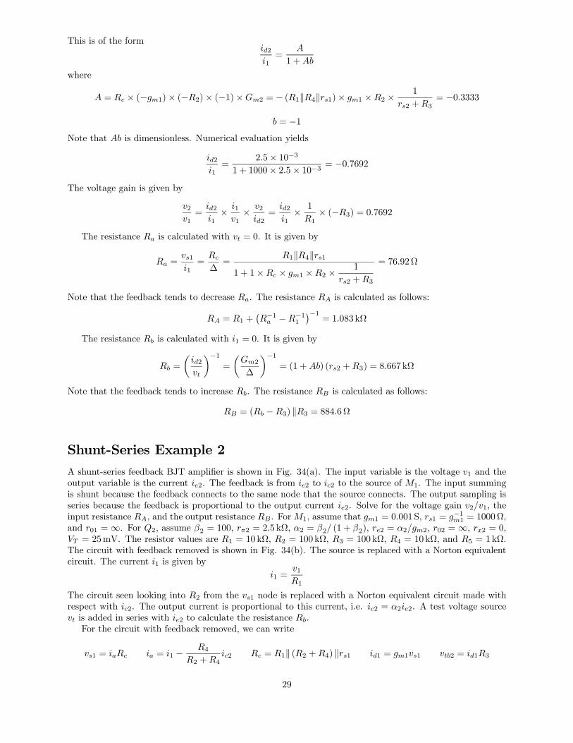
Shunt-Series Example 2A shunt-series feedback BJT amplifier is shown in Fig. 34(a). The input variable is the voltage v1 and theoutput variable is the current ie2. The feedback is from ie2 to ic2 to the source of M1. The input summingis shunt because the feedback connects to the same node that the source connects. The output sampling isseries because the feedback is proportional to the output current ie2. Solve for the voltage gain v2/v1, theinput resistance RA, and the output resistance RB. ForM1, assume that gm1 = 0.001 S, rs1 = g−1m1 = 1000Ω,and r01 =∞. For Q2, assume β2 = 100, rπ2 = 2.5 kΩ, α2 = β2/ (1 + β2), re2 = α2/gm2, r02 =∞, rx2 = 0,VT = 25mV. The resistor values are R1 = 10 kΩ, R2 = 100kΩ, R3 = 100 kΩ, R4 = 10kΩ, and R5 = 1kΩ.The circuit with feedback removed is shown in Fig. 34(b). The source is replaced with a Norton equivalentcircuit. The current i1 is given by
i1 =v1R1
The circuit seen looking into R2 from the vs1 node is replaced with a Norton equivalent circuit made withrespect with ic2. The output current is proportional to this current, i.e. ic2 = α2ie2. A test voltage sourcevt is added in series with ie2 to calculate the resistance Rb.For the circuit with feedback removed, we can write
vs1 = iaRc ia = i1 − R4R2 +R4
ic2 Rc = R1k (R2 +R4) krs1 id1 = gm1vs1 vtb2 = id1R3
29
Figure 34: (a) Shunt-series amplifier. (b) Amplifier with feedback removed.
ie2 = G1vtb2 − vtRd
G1 =1
r0e2 +R5r0e2 =
R31 + β2
+ re2 Rd = R5 + r0e2 ic2 = α2ie2
The equations can be solved algebraically or by a flow graph. The flow graph for the equations is shownin Fig. 35. The determinant is
∆ = 1−µ1×Rc × gm1 ×R3 ×G1 × α2 × −R4
R2 +R4
¶= 1 +Rc × gm1 ×R3 ×G1 × α2 × R4
R2 +R4= 5.025
Figure 35: Signal-flow graph for the equations.
The current gain is
ie2i1
=Rc × gm1 ×R3 ×G1
∆
=Rc × gm1 ×R3 ×G1
1 +Rc × gm1 ×R3 ×G1 × α2 × R4R2 +R4
=
µR1k (R2 +R4) krs1 × gm1 ×R3 × 1
r0e2 +R4
¶1 +
µR1k (R2 +R4) krs1 × gm1 ×R3 × 1
r0e2 +R4
¶× α2 × R4
R2 +R4
30
This is of the formie2i1=
A
1 +Ab
where A and b are given by
A = Rc × gm1 ×R3 ×G1
= R1k (R2 +R4) krs1 × gm1 ×R3 × 1
r0e2 +R4= 44.75
b = α2 × R4R2 +R4
= 0.09
Notice that the product Ab is dimensionless and positive. The latter must be true for the feedback to benegative.Numerical evaluation of the current gain yields
ie2i1=
A
∆= 8.90
The resistances Ra and RA are
Ra =vs1i1=
Rc
∆= 179.3Ω
RA = R1 +¡R−1a −R−11
¢−1= 10.13 kΩ
The resistance Rb and RB are
Rb =
µ−ie2vt
¶−1=
µ1
∆
1
Rd
¶−1= ∆Rd = 10.12 kΩ
RB = (Rb −R5) kR5 = 901.3ΩThe voltage gain is given by
v2v1=
ie2i1× v2
ie2× i1
v1=
A
∆×R2 × 1
R1= 89.0
Shunt-Series Example 3A shunt-series feedback BJT amplifier is shown in Fig. 36(a). The input variable is the voltage v1 andthe output variable is the current ic2. The feedback is from ic2 to ie2 to ic3 to the emitter of Q1. Theinput summing is shunt because the feedback connects to the same node that the source connects. Theoutput sampling is series because the feedback is proportional to the output current ic2. Solve for thevoltage gain v2/v1, the input resistance RA, and the output resistance RB. Assume β = 100, rπ = 2.5 kΩ,α = β/ (1 + β), re = α/gm, r0 = ∞, rx = 0, VT = 25mV. The resistor values are R1 = R3 = 1kΩ andR2 = R4 = R5 = 10 kΩ.The circuit with feedback removed is shown in Fig. 36(b). The source is replaced with a Norton equivalent
circuit consisting of the currenti1 =
v1R1
in parallel with the resistor R1. The feedback is modeled by a Norton equivalent circuit consisting of thecurrent ic3. Because r03 = ∞, the output resistance of this source is an open circuit. The output currentis proportional to this current. Because r02 = ∞, the feedback does not affect the output resistance seenlooking down through R5 because it is infinite. For a finite r02, a test voltage source can be added in serieswith R5 to solve for this resistance. It would be found that a finite r02 considerably complicates the circuitequations and the flow graph.
31
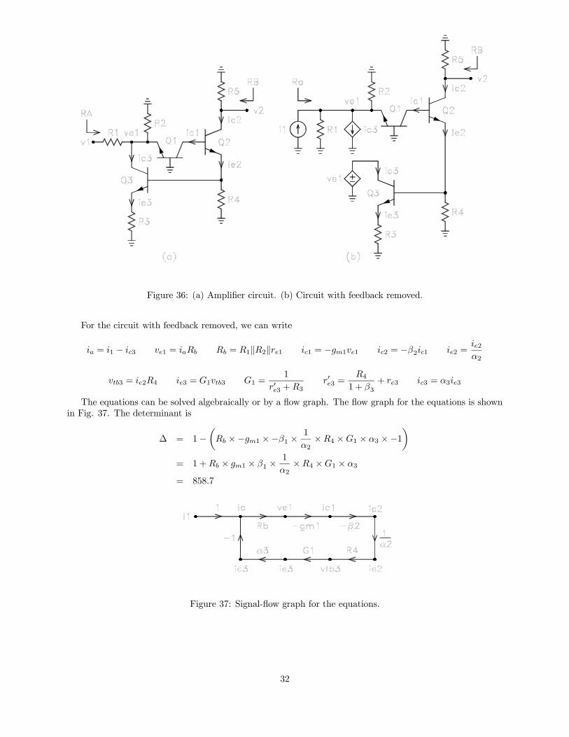
Figure 36: (a) Amplifier circuit. (b) Circuit with feedback removed.
For the circuit with feedback removed, we can write
ia = i1 − ic3 ve1 = iaRb Rb = R1kR2kre1 ic1 = −gm1ve1 ic2 = −β2ic1 ie2 =ie2α2
vtb3 = ie2R4 ie3 = G1vtb3 G1 =1
r0e3 +R3r0e3 =
R41 + β3
+ re3 ic3 = α3ie3
The equations can be solved algebraically or by a flow graph. The flow graph for the equations is shownin Fig. 37. The determinant is
∆ = 1−µRb ×−gm1 ×−β1 ×
1
α2×R4 ×G1 × α3 ×−1
¶= 1 +Rb × gm1 × β1 ×
1
α2×R4 ×G1 × α3
= 858.7
Figure 37: Signal-flow graph for the equations.
32
The transconductance gain is
ic2i1
=1×Rb ×−gm1 ×−β2
∆
=Rb × gm1 × β2
1 +Rb × gm1 × β2 ×1
α2×R4 ×G1 × α3
=(Rb × gm1 × β2)
1 + (Rb × gm1 × β2)×µ1
α2×R4 ×G1 × α3
¶This is of the form
ic2i1=
A
1 +Ab
where A and b are given by
A = Rb × gm1 × β2= R1kR2kre1 × gm1 × β2= 96.39
b =1
α2×R4 ×G1 × α3 =
1
α2×R4 × 1
r0e3 +R3× α3 = 8.899
Notice that the product Ab is dimensionless and positive. The latter must be true for the feedback to benegative.Numerical evaluation of the transconductance gain yields
ic2i1=
A
∆= 0.112
The voltage gain is given by
v2v1=
i1v1× ic2
i1× v2
ic2=
1
R1× A
∆×−R5 = −1.122
The resistances Ra, RA, and RB are given by
Ra =Rb
∆= 0.028Ω RA = R1 +
¡R−1a −R−11
¢−1= 1kΩ RB = R5 = 10kΩ
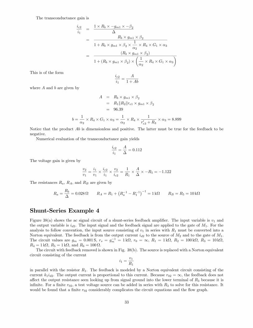
Shunt-Series Example 4Figure 38(a) shows the ac signal circuit of a shunt-series feedback amplifier. The input variable is v1 andthe output variable is id2. The input signal and the feedback signal are applied to the gate of M1. For theanalysis to follow convention, the input source consisting of v1 in series with R1 must be converted into aNorton equivalent. The feedback is from the output current id2 to the source of M2 and to the gate of M1.The circuit values are gm = 0.001 S, rs = g−1m = 1kΩ, r0 = ∞, R1 = 1kΩ, R2 = 100kΩ, R3 = 10kΩ,R4 = 1kΩ, R5 = 1kΩ, and R6 = 100Ω.The circuit with feedback removed is shown in Fig. 38(b). The source is replaced with a Norton equivalent
circuit consisting of the currenti1 =
v1R1
in parallel with the resistor R1. The feedback is modeled by a Norton equivalent circuit consisting of thecurrent k1id2. The output current is proportional to this current. Because r02 =∞, the feedback does notaffect the output resistance seen looking up from signal ground into the lower terminal of R3 because it isinfinite. For a finite r02, a test voltage source can be added in series with R3 to solve for this resistance. Itwould be found that a finite r02 considerably complicates the circuit equations and the flow graph.
33
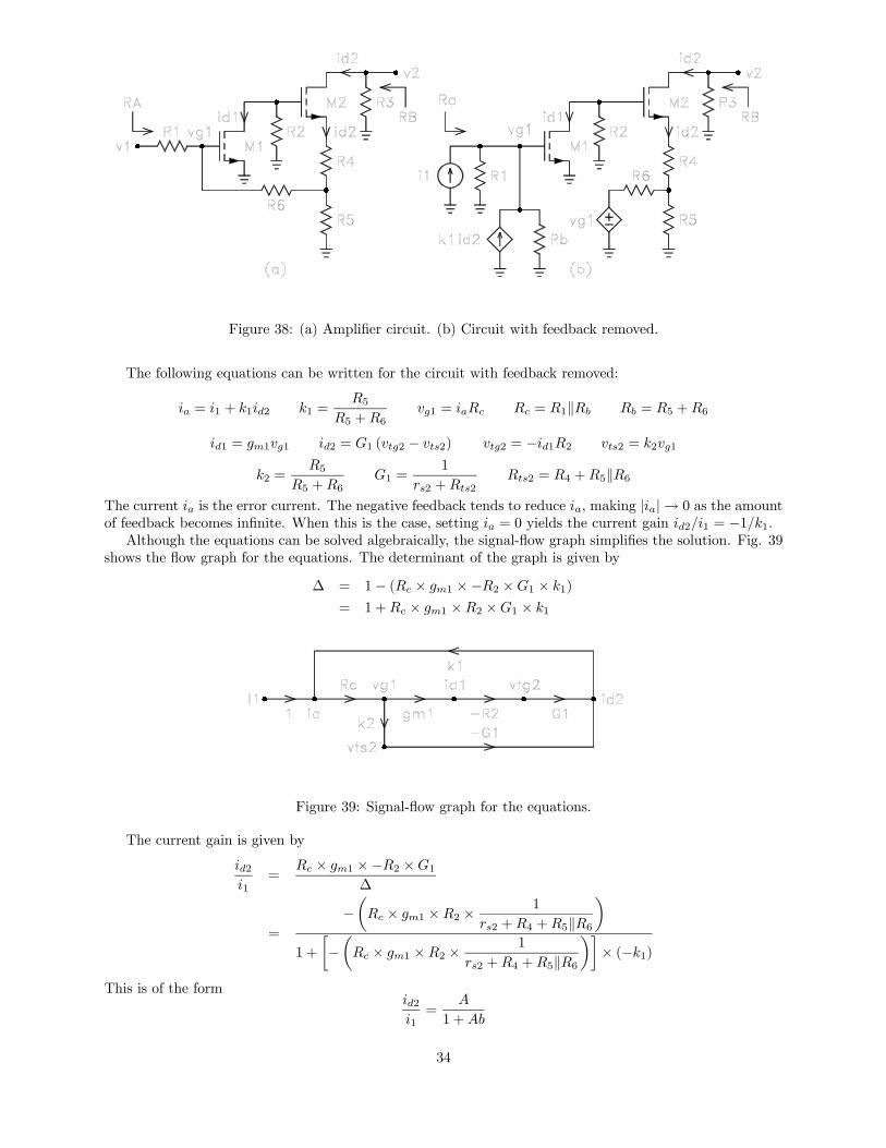
Figure 38: (a) Amplifier circuit. (b) Circuit with feedback removed.
The following equations can be written for the circuit with feedback removed:
ia = i1 + k1id2 k1 =R5
R5 +R6vg1 = iaRc Rc = R1kRb Rb = R5 +R6
id1 = gm1vg1 id2 = G1 (vtg2 − vts2) vtg2 = −id1R2 vts2 = k2vg1
k2 =R5
R5 +R6G1 =
1
rs2 +Rts2Rts2 = R4 +R5kR6
The current ia is the error current. The negative feedback tends to reduce ia, making |ia|→ 0 as the amountof feedback becomes infinite. When this is the case, setting ia = 0 yields the current gain id2/i1 = −1/k1.Although the equations can be solved algebraically, the signal-flow graph simplifies the solution. Fig. 39
shows the flow graph for the equations. The determinant of the graph is given by
∆ = 1− (Rc × gm1 ×−R2 ×G1 × k1)
= 1 +Rc × gm1 ×R2 ×G1 × k1
Figure 39: Signal-flow graph for the equations.
The current gain is given by
id2i1
=Rc × gm1 ×−R2 ×G1
∆
=
−µRc × gm1 ×R2 × 1
rs2 +R4 +R5kR6
¶1 +
·−µRc × gm1 ×R2 × 1
rs2 +R4 +R5kR6
¶¸× (−k1)
This is of the formid2i1=
A
1 +Ab
34
where
A = −µRc × gm1 ×R2 × 1
rs2 +R4 +R5kR6
¶= −25.02
b = −k1 = −0.909Note that Ab is dimensionless. Numerical evaluation yields
id2i1=
−25.021 + (−25.02)× (−0.909) = −1.054
The voltage gain is given by
v2v1=
id2i1× i1
v1× v2
id2=
id2i1× 1
R1×−R3 = −10.54
The resistance Ra is
Ra =vs1i1=
Rc
∆=
R1k (R5 +R6)
∆= 22.03Ω
Note that the feedback tends to decrease Ra. The resistance RA is
RA = R1 +¡R−1a −R−11
¢−1= 1.023 kΩ
The resistance RB isRB = R3 = 10 kΩ
This is not a function of the feedback because r02 has been assumed to be infinite.
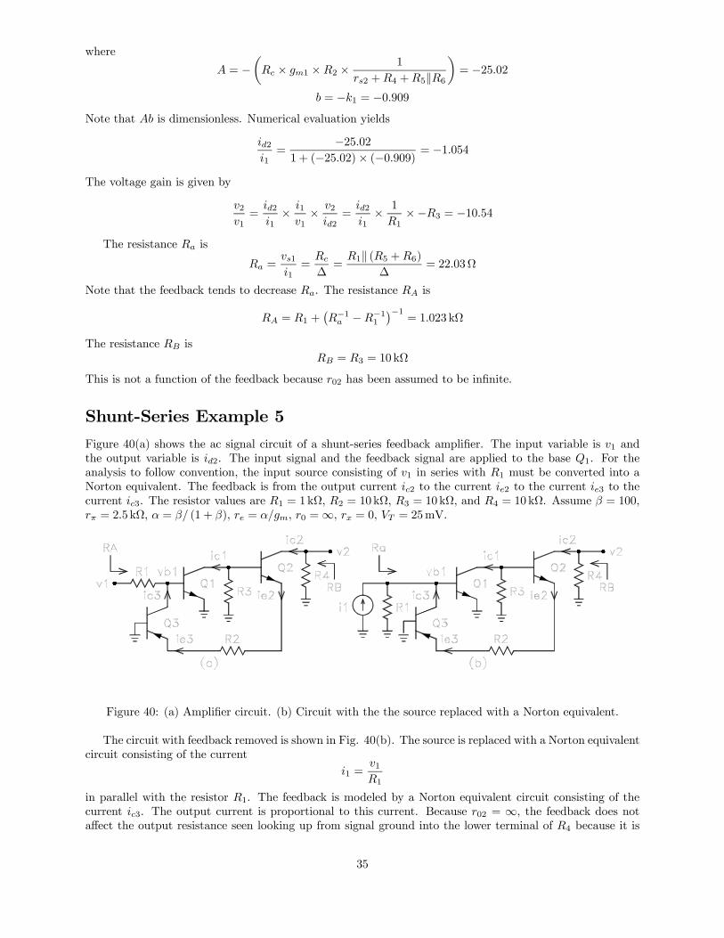
Shunt-Series Example 5Figure 40(a) shows the ac signal circuit of a shunt-series feedback amplifier. The input variable is v1 andthe output variable is id2. The input signal and the feedback signal are applied to the base Q1. For theanalysis to follow convention, the input source consisting of v1 in series with R1 must be converted into aNorton equivalent. The feedback is from the output current ic2 to the current ie2 to the current ie3 to thecurrent ic3. The resistor values are R1 = 1kΩ, R2 = 10kΩ, R3 = 10kΩ, and R4 = 10 kΩ. Assume β = 100,rπ = 2.5 kΩ, α = β/ (1 + β), re = α/gm, r0 =∞, rx = 0, VT = 25mV.
Figure 40: (a) Amplifier circuit. (b) Circuit with the the source replaced with a Norton equivalent.
The circuit with feedback removed is shown in Fig. 40(b). The source is replaced with a Norton equivalentcircuit consisting of the current
i1 =v1R1
in parallel with the resistor R1. The feedback is modeled by a Norton equivalent circuit consisting of thecurrent ic3. The output current is proportional to this current. Because r02 = ∞, the feedback does notaffect the output resistance seen looking up from signal ground into the lower terminal of R4 because it is
35
infinite. For a finite r02, a test voltage source can be added in series with R4 to solve for this resistance. Itwould be found that a finite r02 considerably complicates the circuit equations and the flow graph.The following equations can be written for the circuit with feedback removed:
ia = i1 + ic3 vb1 = iaRb Rb = R1krπ1 ic1 = gm1vb1 vtb2 = −ic1R3 ie2 = G1vtb2
G1 =1
r0e2 +R2 + re3r0e2 =
R31 + β2
+ re2 ic2 = α2ie2 ie3 = ie2 ic3 = α3ie3
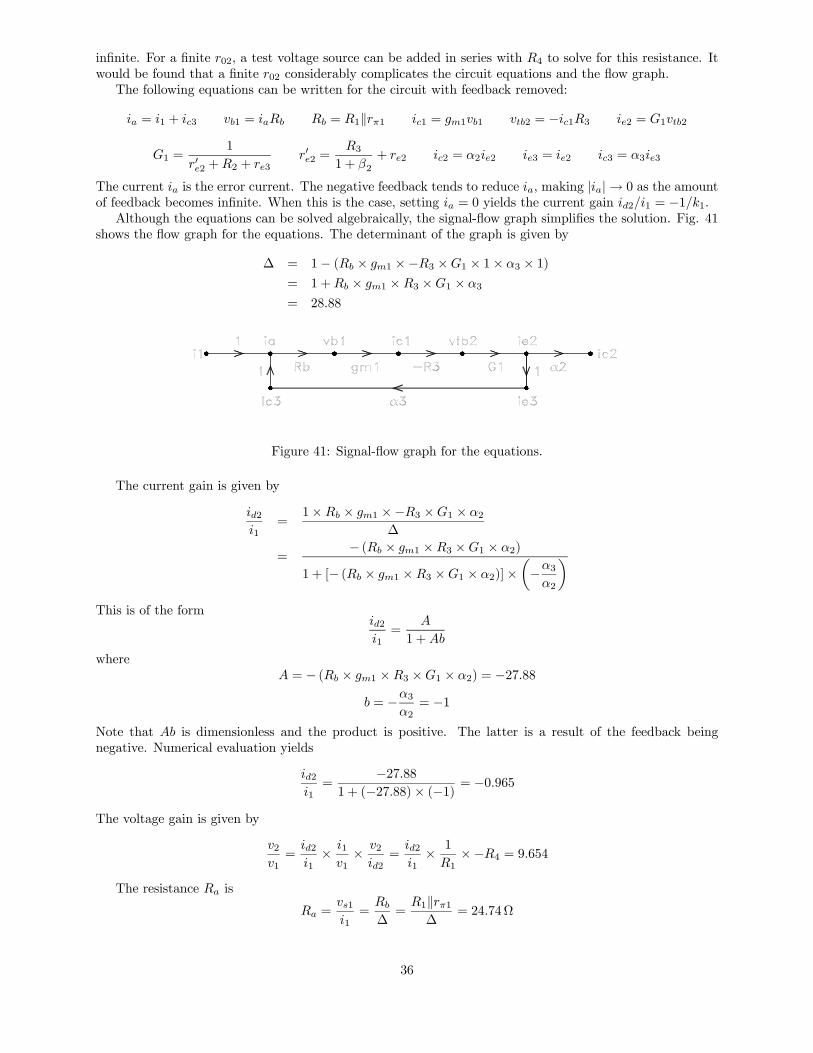
The current ia is the error current. The negative feedback tends to reduce ia, making |ia|→ 0 as the amountof feedback becomes infinite. When this is the case, setting ia = 0 yields the current gain id2/i1 = −1/k1.Although the equations can be solved algebraically, the signal-flow graph simplifies the solution. Fig. 41
shows the flow graph for the equations. The determinant of the graph is given by
∆ = 1− (Rb × gm1 ×−R3 ×G1 × 1× α3 × 1)= 1 +Rb × gm1 ×R3 ×G1 × α3
= 28.88
Figure 41: Signal-flow graph for the equations.
The current gain is given by
id2i1
=1×Rb × gm1 ×−R3 ×G1 × α2
∆
=− (Rb × gm1 ×R3 ×G1 × α2)
1 + [− (Rb × gm1 ×R3 ×G1 × α2)]×µ−α3α2
¶This is of the form
id2i1=
A
1 +Ab
whereA = − (Rb × gm1 ×R3 ×G1 × α2) = −27.88
b = −α3α2= −1
Note that Ab is dimensionless and the product is positive. The latter is a result of the feedback beingnegative. Numerical evaluation yields
id2i1=
−27.881 + (−27.88)× (−1) = −0.965
The voltage gain is given by
v2v1=
id2i1× i1
v1× v2
id2=
id2i1× 1
R1×−R4 = 9.654
The resistance Ra is
Ra =vs1i1=
Rb
∆=
R1krπ1∆
= 24.74Ω
36
Note that the feedback tends to decrease Ra. The resistance RA is
RA = R1 +¡R−1a −R−11
¢−1= 1.025 kΩ
The resistance RB isRB = R4 = 10 kΩ
This is not a function of the feedback because r02 has been assumed to be infinite.
37


