
Coherent electrical readout of defect spins in 4H-SiC by ... · a long-lived metastable state gives...
34
Coherent electrical readout of defect spins in 4H-SiC by photo-ionization at ambient conditions Matthias Niethammer, *,† Matthias Widmann, † Torsten Rendler, † Naoya Morioka, † Yu-Chen Chen, † RainerSt¨ohr, † Jawad Ul Hassan, ‡ Shinobu Onoda, ¶ Takeshi Ohshima, ¶ Sang-Yun Lee, § Amlan Mukherjee, † Junichi Isoya, k Nguyen Tien Son, ‡ and J¨org Wrachtrup †,⊥ †3rd Institute of Physics and Center for Applied Quantum Technologies, University of Stuttgart, 70569 Stuttgart, Germany ‡Department of Physic, Chemistry and Biology, Link¨ oping University, SE-581 83 Link¨ oping, Sweden ¶National Institutes for Quantum and Radiological Science and Technology, Takasaki 370-1292, Japan §Center for Quantum Information, Korea Institute of Science and Technology, Seoul 02792, Republic of Korea kFaculty of Pure and Applied Sciences, University of Tsukuba, Tsukuba 305-8573, Japan ⊥Max Planck Institute for Solid State Research, 70569 Stuttgart, Germany E-mail: [email protected] Abstract Quantum technology relies on proper hardware, enabling coherent quantum state control as well as efficient quantum state readout. In this regard, wide-bandgap semi- conductors are an emerging material platform with scalable wafer fabrication methods, 1 arXiv:1903.12236v1 [cond-mat.mes-hall] 28 Mar 2019
Transcript of Coherent electrical readout of defect spins in 4H-SiC by ... · a long-lived metastable state gives...

Coherent electrical readout of defect spins in
4H-SiC by photo-ionization at ambient conditions
Matthias Niethammer,∗,† Matthias Widmann,† Torsten Rendler,† Naoya
Morioka,† Yu-Chen Chen,† Rainer Stohr,† Jawad Ul Hassan,‡ Shinobu Onoda,¶
Takeshi Ohshima,¶ Sang-Yun Lee,§ Amlan Mukherjee,† Junichi Isoya,‖ Nguyen
Tien Son,‡ and Jorg Wrachtrup†,⊥
†3rd Institute of Physics and Center for Applied Quantum Technologies, University of
Stuttgart, 70569 Stuttgart, Germany
‡Department of Physic, Chemistry and Biology, Linkoping University, SE-581 83
Linkoping, Sweden
¶National Institutes for Quantum and Radiological Science and Technology, Takasaki
370-1292, Japan
§Center for Quantum Information, Korea Institute of Science and Technology, Seoul
02792, Republic of Korea
‖Faculty of Pure and Applied Sciences, University of Tsukuba, Tsukuba 305-8573, Japan
⊥Max Planck Institute for Solid State Research, 70569 Stuttgart, Germany
E-mail: [email protected]
Abstract
Quantum technology relies on proper hardware, enabling coherent quantum state
control as well as efficient quantum state readout. In this regard, wide-bandgap semi-
conductors are an emerging material platform with scalable wafer fabrication methods,
1
arX
iv:1
903.
1223
6v1
[co
nd-m
at.m
es-h
all]
28
Mar
201
9

hosting several promising spin-active point defects. Conventional readout protocols for
such defect spins rely on fluorescence detection and are limited by a low photon collec-
tion efficiency. Here, we demonstrate a photo-electrical detection technique for electron
spins of silicon vacancy ensembles in the 4H polytype of silicon carbide (SiC). Further,
we show coherent spin state control, proving that this electrical readout technique en-
ables detection of coherent spin motion. Our readout works at ambient conditions,
while other electrical readout approaches are often limited to low temperatures or
high magnetic fields. Considering the excellent maturity of SiC electronics with the
outstanding coherence properties of SiC defects the approach presented here holds
promises for scalability of future SiC quantum devices.
Keywords
silicon vacancy center, silicon carbide, PDMR, ODMR, electrical readout, coherent control
Main text
Solid state color centers have developed into a leading contender in quantum technology
owing to their vast potential as hardware for quantum sensing and quantum networks.1–6
Typically, these techniques employ optical control for spin state initialization and readout.
Spins in solids can provide long spin relaxation and dephasing times and therefore constitute
excellent quantum bits. In certain cases, e.g. for spins in wide-bandgap semiconductors, sin-
gle spin manipulation and optical spin state readout is feasible.7–10 A number of systems,
like spin dopants in silicon11–13 or quantum dots,14,15 allow for electrical spin readout. How-
ever, because their spin polarization typically relies on Boltzmann statistics, they require
low temperature operation or large magnetic fields.16
In contrast, color centers in wide-bandgap semiconductors show efficient optical spin
polarization at room temperature.17,18 Electrical readout of color center spins at ambient
2

conditions relies on an efficient mechanism for spin-to-current conversion. This can be real-
ized by measuring a laser induced spin-dependent photocurrent, which is often referred to
as photocurrent detected magnetic resonance (PDMR). Several publications have success-
fully demonstrated this principle for various materials.19–22 Recently, this technique has been
applied to the nitrogen-vacancy (NV) center in diamond, by combining electrical readout
with optical excitation23,24 and even achieved single defect25 detection. It turns out that
the signal-to-noise ratio (SNR) in this approach is competitive to optical detection25 and
at the same time allows better integration into electronic periphery. However, diamond
as host material is not compatible with industrial technologies, e.g. large-scale wafers and
the development of efficient diamond electronics is still subject to research. Silicon carbide
(SiC) on the other hand has attracted attention due to its outstanding optical, electrical and
mechanical properties.3
Traditionally, interest in defects in SiC was driven by their impeding properties to high
power electronic devices.26 This has initialized a wealth of studies utilizing electron paramag-
netic resonance27,28 and electrically detected magnetic resonance.29–33 Among many investi-
gated phenomena, spin dependent recombination has been shown to allow for self-calibrating
magnetometers in a non-coherent fashion.34 In addition, several spin-active defects with long
spin coherence times10,35 even at room temperature9,36 have been found. The quantum prop-
erties of such color centers have lately been used to demonstrate magnetic field and temper-
ature sensing.37–40 In this work, we demonstrate electrical readout of a negatively charged
silicon-vacancy (V−Si) spin ensemble in a 4H-SiC device via PDMR at ambient conditions.
The negatively charged silicon vacancy V−Si at the cubic lattice site (V2) in 4H-SiC pro-
vides both, stable deep level energy states in a wide-bandgap host and a spin dependent
intersystem crossing (ISC). Previous studies revealed, that the defect has a spin quartet
manifold of S=3/228,41 in ground state (GS) and excited state (ES), which are separated by
1.35 eV (916 nm).42 GS and ES Lande g-factors are identical (g=2.003) and their respective
zero field splittings (ZFS) are 70 MHz and ≈410 MHz43 at ambient conditions. In addition,
3
a long-lived metastable state gives rise to non-radiative and spin-dependent ISC relaxation,
enabling optical spin state initialization and readout under ambient conditions.9,42,44 Fur-
thermore, it provides excellent coherence times even at room-temperature.9,36,45
In the following, we discuss the principle of PDMR and how it can be applied to V−Si.
Figs. 1(a)-(c) depict the underlying charge dynamics: a deep level defect absorbs a photon
and is promoted from its GS to the ES. From there: (i) The system can decay back to
the GS by emitting a photon. (ii) The system can undergo a non-radiative ISC via a
metastable state (MS). A spin-state dependency of this ISC rate is usually exploited in
optically detected magnetic resonance (ODMR). (iii) While being in the ES, the system can
undergo a second optical excitation to the conduction band (CB). In case (iii), an excess
electron populates the CB, and the defect charge state n is changed to n + 1. To reach a
steady-state charge distribution, the defect can re-capture an electron either from the CB,
or from other recharging sources, e.g. from other defects in the surrounding, or from the
valance band (VB) through photo-induced electron-hole pair generation. In the third case,
the free electron in the CB and the hole in the VB can be measured as photocurrent.
If the ISC rates are spin-dependent, this charge circulation enables photo-electrical spin-
state readout. Note that the second photon may also be absorbed by the MS during an ISC
cycle. Because the overall lifetime in the ES and MS is determined by the ISC as well, the
spin dependency of the ISC rate alters the chance for the second photon absorption. The
amount of spin-dependent contribution to photocurrent by this process is then expected to
be the sum of currents created by promoting an electron either from the ES or MS to the
CB.
We assume the V−Si to be initialized in the ±1/2 spin subspace of the GS by optical
illumination. During optical excitation, the ES is populated. If the ISC rate from ES to MS
states is higher for ±1/2 than for the ±3/2 states, the chance for two-photon absorption
from the ES of ±3/2 states is higher.
Populating the ±3/2 states by resonantly driving the spin transition will consequently
4

increase the photocurrent. For an ionization from the MS to CB, a decrease in current should
be measured. The overall sign and magnitude of the effect will thus be determined by the
difference in absorption cross section, ISC rates, lifetime and population of the ES and MS.
(c)
1/2
GS
ES
MS
recharging
0.7 eV
1.4 eV
0.9 eV
3/2
1/23/2
1/2
GS
ES
MS
3/2
1/23/2
1/2
GS
ES
MS
3/2
1/23/2
(b)
laser
lock-in
RF
time
(a)
(d)
ISC ISCISC
hν
hν
(hν)
Figure 1: PDMR mechanism and readout. (a)-(c) Spin-dependent photo-ionization. (a)Single photon excitation. ES can relax to either GS or MS. ISC to MS is dependent on thespin state in ES, thus GS is polarized. (b) Second photon ionizes the defect and introducesa free electron in the CB. (c) Recharging of the defect from VB and separation of chargeslead to a photocurrent. (d) Pulse sequence scheme used for lock-in detection. See text fordetail.
The microstructure used in this work is a n++/n−/n++ metal-semiconductor-metal (MSM)
junction, which is shown in Fig. 2(a). Starting from a n-type 4H-SiC substrate, epitaxial
growth was used to fabricate a three-layer stack: (i) a 10 µm-thick vanadium-doped semi-
insulating layer to reduce leakage currents into the substrate, (ii) a 10 µm-thick n− layer with
N-doping concentration of 1× 1014 cm−3, and (iii) a 400 nm-thick n++ layer with N-doping
5

concentration of 8× 1017 cm−3. A nickel (Ni) layer of 100 nm thickness was deposited form-
ing a Schottky contact on the n++ layer. The sample was etched down by 10 µm, leaving
fingers of various width as devices. Subsequently, the Ni and n++ films were removed in rect-
angular center areas of various sizes, for optical access to the n− region (see zoomed inset
in Fig. 2(a)). In this layer, we expect the charge state of the V−Si to be stable. Additionally,
gold is deposited on the contact pads for wire bonding (see Supporting Information). Af-
Bias
TIA
100µm
Au padNi contact
n layer++
n layer_
sem
i-in
sula
ting(a) (b)
(c) (d)
Figure 2: (a) SEM picture (functional layers false color coded) of a fabricated device. Biasand transimpedance amplifier (TIA) connections are marked. Inset: Zoom-in of the etchedoptical opening. (b) Photocurrent map at -10 V bias. Approximate position of opticalaccess opening marked in red. (c) Laser power dependence of the photocurrent at theposition of maximum two-photon contribution corresponding to a bright spot in (d). Fitf(x) = ax2 + bx separates linear and quadratic contributions, where x stands for opticalpower. Fit parameters are: a=117.77 ± 6.43 fA/mW2, b=10.96 ± 0.93 pA/mW. (d) Map oftwo-photon excitation contribution to photocurrent at maximum laser power obtained viafit parameter a.
6

ter recording I–V curves of the device, we create a V−Si ensemble by electron irradiation at
2 MeV with a dose of 1× 1017 cm−2. This process degrades the contact quality and device
conductivity due to carrier compensation46 (see Supporting Information). However, this also
results in minimizing the dark current, enabling us to maximize the amplifier gain, which is
beneficial for electrical readout. We chose to perform measurements on a device with 10 µm
× 12 µm active area.
Optical excitation is performed with a 785 nm laser (Toptica, iBeam smart), which is
focused onto the SiC device using an NA=0.65 objective (Zeiss, Plan-Achromat 40×). The
sample is mounted on a 3D piezo stage with 100 µm travel range (Physik Instrumente,
P-561.3CD). A 3D Helmholtz coil arrangement is used for applying magnetic fields in ar-
bitrary directions. Radiofrequency (RF) for spin control and manipulation are provided
by a rubidium-referenced (EFRATOM, LPRO-101) signal generator (Rohde & Schwarz,
SMIQ03B), pulsed by a microwave switch (Mini Circuits, ZASWA-2-50D), amplified (Mini
Circuits, ZHL4240W) and finally applied via a coplanar waveguide on the printed circuit-
board sample holder below the sample. This sample holder also incorporates contact pads,
to which the device contacts are wire-bonded. For better SNR, we use a lock-in detection
scheme (Stanford Research, SR830). Therefore the signal is locked to the laser pulses for
photocurrent measurements and on the modulated RF pulses for ODMR, PDMR and Rabi
measurements). As the RF pulses are short (300 ns), the locking is achieved by repeating
the whole spin control pulse sequences with and without RF multiple times at a lock-in
frequency of 429 Hz, as depicted in Fig. 1(d). Typical pulse lengths for optical initialization
in PDMR are 600 ns laser pulse followed by 1 µs settling time.
To measure a spin-dependent photocurrent, a bias voltage is applied using a source
measure unit (Keithley, 2636B). The resulting photocurrent is converted to a voltage by a
transimpedance amplifier (Femto, DLPCA-200, gain of 108 for PDMR, 109 for Rabi), which
is low-pass filtered at 1 kHz. By scanning the sample position, we record photocurrent maps.
At each position, we measure the photocurrent as a function of excitation power and fit the
7
recorded data with a second order polynomial function to infer the contributions of single-
(linear) and two-photon (quadratic) processes. For ODMR measurements, we detect fluo-
rescence emission from 850 nm to 950 nm using a photodiode (Newport, Model 2151) and
feed the signal directly into the lock-in amplifier. All measurements are performed at a laser
power of 178.5 mW (unless stated otherwise) in order to keep the same experimental condi-
tions for PDMR and ODMR. The beam in front of the photodiode is attenuated by an iris
to prevent detector saturation. For PDMR measurements, the output of the transimpedance
amplifier is connected to the lock-in amplifier instead of the photodiode. To avoid artefacts
due to frequency-dependent coupling into the SiC device, we keep the RF frequency constant
and stepwise change the magnetic field B0 revealing the magnetic resonance induced signals.
The magnetic field is roughly aligned along the c-axis of the sample. In order to map the
PDMR signal, we repeatedly measure and average the PDMR amplitude. This is done by
subtracting the off-resonant signal from the on-resonance data. The off-resonant signal is
obtained at a B0-field strength corresponding to 23 MHz detuning.
A similar approach is used for spin Rabi oscillation measurements. Here, a fixed B0 field
is applied and a RF field (B1 field) at the spin resonance frequency drives the system, while
the RF pulse length is altered and the overall sequence duration is kept constant. To account
for potential RF pick-up by the lock-in scheme, we subtract an off-resonant baseline signal
as described for the PDMR mapping.
Fig. 2(b) shows the photocurrent map of our device. We find that the response is localized
inside the center of the device. The spatial map of the contribution of two-photon process
in the photocurrent extracted from quadratic fitting of the laser power dependency of pho-
tocurrent data (see Fig. 2(c)) is shown in Fig. 2(d). Comparing Fig. 2(b) with Fig. 2(d), we
find that most areas show mainly linear response, indicating single photon absorption from
shallow traps. In the center of the device, we observe a pronounced quadratic dependence.
We perform all further measurements in this area.
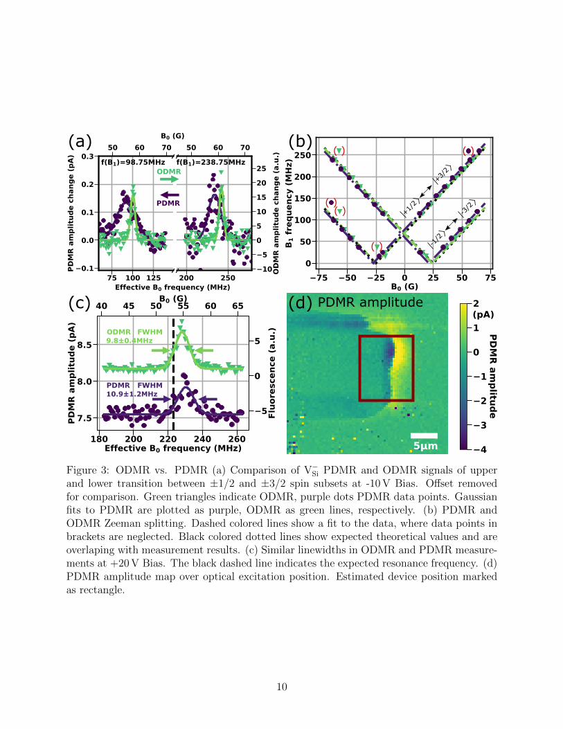
We subsequently perform stepwise B0-field dependent measurements at fixed RF fre-
8

quencies of 98.75 MHz and 238.75 MHz to resolve the resonances of −1/2↔ −3/2 and +1/2
↔ +3/2 transitions, respectively. Both PDMR and ODMR results are shown in Fig. 3(a),
exhibiting the expected magnetic resonance for both ODMR and PDMR except for a small
difference in the resonance positions. We tend to attribute the shift between ODMR and
PDMR resonance to offset fields present in the device, probably due to the proximity to
the ferromagnetic Ni contacts (see Supporting Information). As an ensemble is used and
field inhomogenities are present, lines are expected to be of Gaussian shape envelope. The
linewidths in Fig. 3(a) are much broader in the electrical case compared to the optically
detected lines. We attribute this to a mismatch in the detection volumes for both techniques
in combination with the residual magnetization of the Ni contacts. As the fluorescence light
is not spatially filtered in case of the electrical readout, the detected signal may differ in
position compared to the ODMR measurements. Nonetheless, data recorded at a different
position shown in Fig. 3(c) suggests similar linewidths for PDMR and ODMR and thus
proves that broadening in Fig. 3(a) is not due to the PDMR technique (see Supporting
Information). To check that the measured signal originates from V2 centers, we measure
the ground state ZFS via Zeeman splitting measurements by observing the resonances at
various magnetic fields. As depicted in Fig. 3(b), the ZFS is found by fitting the model
function fres(B0) = |ZFS± gµB (B0 +Boffset)| to the magnetic field dependence of the reso-
nances. Thereby, g is the effective electron Lande factor for V−Si, µB is the Bohr magneton
and Boffset is a magnetic field accounting for the device internal fields. With this, we find
ZFSODMR = 69.0 ± 0.3 MHz and ZFSPDMR = 69.1 ± 0.3 MHz for the optically and electri-
cally detected case, respectively. The g factors found by the fit are gODMR = 2.02 ± 0.01
for ODMR and gPDMR = 2.03 ± 0.01 for PDMR, while the offset field is Boffset,ODMR = 0.4
± 0.1 and Boffset,PDMR = 3.0 ± 0.1 G, respectively. The data presented corroborate that the
signal originates from V2 centers. As shown in Fig. 3(d), the PDMR signal is located in the
same area where the two-photon photocurrent contribution was found in Fig. 2(d). However,
we find the sign of the PDMR signal to be dependent on the location within the device as
9
PDMR amplitude
(a) (b)
(d)(c)
( ) ( )
( )( )
( ) -1/2
-3/2
+1/
2
+3/
2
FWHM
10.9±1.2MHz
FWHM
9.8±0.4MHz
Figure 3: ODMR vs. PDMR (a) Comparison of V−Si PDMR and ODMR signals of upper
and lower transition between ±1/2 and ±3/2 spin subsets at -10 V Bias. Offset removedfor comparison. Green triangles indicate ODMR, purple dots PDMR data points. Gaussianfits to PDMR are plotted as purple, ODMR as green lines, respectively. (b) PDMR andODMR Zeeman splitting. Dashed colored lines show a fit to the data, where data points inbrackets are neglected. Black colored dotted lines show expected theoretical values and areoverlaping with measurement results. (c) Similar linewidths in ODMR and PDMR measure-ments at +20 V Bias. The black dashed line indicates the expected resonance frequency. (d)PDMR amplitude map over optical excitation position. Estimated device position markedas rectangle.
10
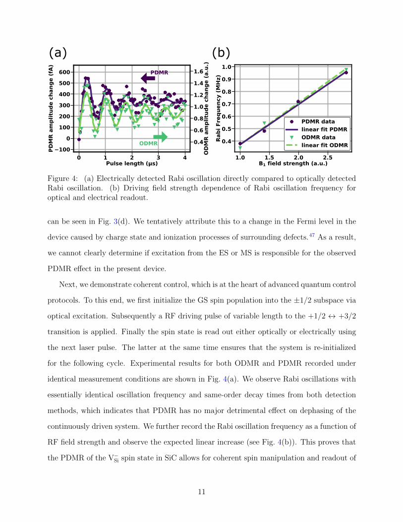
(a) (b)
Figure 4: (a) Electrically detected Rabi oscillation directly compared to optically detectedRabi oscillation. (b) Driving field strength dependence of Rabi oscillation frequency foroptical and electrical readout.
can be seen in Fig. 3(d). We tentatively attribute this to a change in the Fermi level in the
device caused by charge state and ionization processes of surrounding defects.47 As a result,
we cannot clearly determine if excitation from the ES or MS is responsible for the observed
PDMR effect in the present device.
Next, we demonstrate coherent control, which is at the heart of advanced quantum control
protocols. To this end, we first initialize the GS spin population into the ±1/2 subspace via
optical excitation. Subsequently a RF driving pulse of variable length to the +1/2 ↔ +3/2
transition is applied. Finally the spin state is read out either optically or electrically using
the next laser pulse. The latter at the same time ensures that the system is re-initialized
for the following cycle. Experimental results for both ODMR and PDMR recorded under
identical measurement conditions are shown in Fig. 4(a). We observe Rabi oscillations with
essentially identical oscillation frequency and same-order decay times from both detection
methods, which indicates that PDMR has no major detrimental effect on dephasing of the
continuously driven system. We further record the Rabi oscillation frequency as a function of
RF field strength and observe the expected linear increase (see Fig. 4(b)). This proves that
the PDMR of the V−Si spin state in SiC allows for coherent spin manipulation and readout of
11

the ground state and thus fulfills the fundamental requirements for more complex quantum
control schemes.
To evaluate the performance of the PDMR technique, we performed a parameter depen-
dency study (see Supporting Information). We find a ten-fold increase in SNR in ODMR
compared to PDMR after normalizing to the same measurement time. In addition, the
PDMR contrast is around one order of magnitude smaller than the ODMR contrast with
the current device. While PDMR amplitudes are in the range of pA, the mean dc back-
ground current measured by an oscilloscope parallel to the lock-in amplifier is on the order
of a few nA. This results in a typical contrast of 0.03 %. On the other hand, ODMR mea-
surements yield a contrast of around 0.1 %. The background current mainly consists of the
resistive current through the device due to the bias. The laser induced photocurrent also
contributes to the background, but due to the pulsed type of measurement is decreased by
the duty cycle. However, our measurements suggest that we are limited by the current ex-
perimental conditions and that multiple parameters can still be optimized (see Supporting
Information). Especially with increasing laser power the ODMR contrast saturates, whereas
no saturation behavior is observed for PDMR yet. This is consistent with findings for NV
ensembles in diamond.23 Furthermore, refining the measurement technique and device struc-
ture can potentially improve SNR. A large contribution to the noise floor is stray RF fields.
We anticipate a gain in SNR by improving the device structure to be more resilient against
parasitic RF coupling. In addition, the stepwise measurement was done in a conservative
way and seconds of settling time between magnetic field steps were chosen in order to reach a
quasi-static situation, while lock-in integration time was set to 30 ms. Using a real magnetic-
field sweep or frequency-modulated RF field will speed up signal accumulation. However,
due to the RF-frequency-dependent stray currents and no possibility to directly sweep the
magnetic field in our experimental conditions, we have not incorporated such techniques
yet. Moreover, changes to the doping profile may allow to enhance carrier extraction effi-
ciency, but may come with the cost of an increase in background photocurrent. As the large
12
bandgap hinders a two-photon band-to-band excitation with a 785 nm laser, the background
photocurrent is likely generated by excitation of other intra-band defects created besides
the V−Si ensemble during the electron irradiation. As the background limits transimpedance
gain, a trade-off between signal extraction efficiency and background has to be found. An-
other parameter is device geometry, e.g. channel width and thickness of the active layer. By
this, the detection volume might be enlarged and leakage currents further reduced. Inter-
estingly, only a small area within the aperture shows contribution to PDMR, although the
details of the process have to be understood first. To this end, we suggest to measure the
dependence of the signal on excitation laser wavelength and pulse length, which might give
insight into the ionization process and may ultimately improve readout fidelity and state
preparation.48,49 Since we have shown that coherent spin control of V−Si can be combined
with PDMR, phase interferometry type sensing protocols can be utilized, which can boost
sensitivity in metrology applications by many orders of magnitude.50,51
In summary, we have demonstrated photo-electrical readout of a V−Si spin ensemble in a
4H-SiC metal-semiconductor-metal device under ambient conditions. We also report elec-
trically detected spin coherence of this ensemble. This underlines the great potential of SiC
and PDMR for quantum applications. The availability of large wafer production and pro-
cessing techniques are very promising to future integration of electrical quantum devices at
an industrially relevant scale. Advanced fabrication techniques can be used to integrate e.g.
high-performance CMOS transimpedance amplifiers on-chip.52 This would allow miniatur-
ization and quantum device integration into a classical circuit design. Even integration of
the optical light source might be feasible in the future.53 Altogether, this work provides a
first step towards integrated electrical quantum devices in 4H-SiC for quantum technology.
13

Author contributions
The initial planning of the project was done by M.N., M.W., S.-Y.L, N.T.S. and J.W.. J.U-H.
and N.T.S. designed the device structure and performed the sample growth. R.S. fabricated
the device. S.O., T.O. and J.I. planned and performed electron irradiation. M.N. designed
and performed all experiments. M.N., T.R., M.W., A.M., N.M., Y-C.C., S.-Y.L and J.W.
analyzed the data. The manuscript was written by M.N., M.W., T.R., R.S. and J.W. with
contribution from all of the authors.
Acknowledgments
The authors thank Florian Kaiser for his valuable help in preparing the manuscript. We
acknowledge financial support by the EU (ASTERIQS and ERC SMeL), BMBF (Brain-
QSens), the Max Planck Society, the Volkswagen Foundation, the Swedish Research Council
(VR 2016-04068 and VR 2016-05362), the Carl Tryggers Stiftelse for Vetenskaplig Forskn-
ing (CTS 15:339), the Swedish Energy Agency (43611-1), the Knut and Alice Wallenberg
Foundation (KAW 2018.0071), the Korea Institute of Science and Technology institutional
programs (2E27231, 2E29580) and the Japan Society for the Promotion of Science KAK-
ENHI (17H01056).
Abbreviations
CB – conduction band
ES – excited state
GS – ground state
ISC – intersystem crossing
MS – metastable state
MSM – metal-semiconductor-metal structure
14

NV – nitrogen-vacancy center in diamond
ODMR – optically detected magnetic resonance
PDMR – photocurrent detected magnetic resonance
RF – radiofrequency
SiC – silicon carbide
SNR – signal-to-noise ratio
TIA – transimpedance amplifier
VB – valence band
V−Si, V2 – negatively charged silicon-vacancy (at cubic lattice site)
ZFS – zero field splittings
Supporting Information
April 1, 2019
15
Supporting information
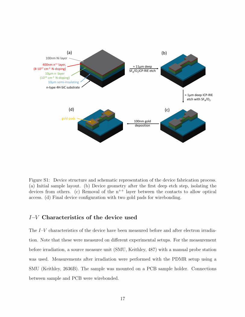
Sample growth and fabrication details
Different layers were grown by chemical vapor deposition (CVD) on 4° off-axis n-type 4H-SiC
substrate. The first layer grown is a 10 µm thick semi-insulating V-doped layer followed by
a n− layer (10 µm) with a free carrier concentration of 1× 1014 cm−3 at room temperature.
The top n++-type N-doped contact layer is 400 nm thick with a doping concentration of
8× 1017 cm−3.
Fig. S1(a) shows the sample layout before structuring. While the Ni layer serves as a
Schottky contact in the final device, it is also used as an etching mask during the fabrication
process. All dry etching steps are performed using an ICP-RIE with SF6/O2 gas mixture,
which realizes high etching selectivity of SiC over Ni. In the first step, all Ni outside the
device region is removed. The sample is then plasma-etched ≈11 µm deep, which removes
the n++ layer and the n− layer and stops in the semi-insulating layer (Fig. S1(b)). During
this step, the device region is protected by the residual Ni layer. Subsequently, Ni is removed
in a rectangular region between the two contact pads of the device. This allows to etch the
n++ layer in this region by a short SF6/O2 ICP-RIE plasma step. The etching depth is
chosen to be roughly twice the thickness of the n++ layer, ensuring that it is completely
removed. Finally, gold pads are deposited on both contacts for wirebonding, resulting in the
final device as depicted in Fig. S1(d).
16
10µm semi‐insulating
10µm n‐ layer(1014 cm‐3 N‐doping)
400nm n++ layer,(8∙1017 cm‐3 N‐doping)
100nm Ni layer
n‐type 4H‐SiC substrate
≈ 11µm deepSF6/O2ICP‐RIE etch
≈ 1µm deep ICP‐RIEetch with SF6/O2
100nm golddeposition
(a)
(d) (c)
(b)
gold pads
Figure S1: Device structure and schematic representation of the device fabrication process.(a) Initial sample layout. (b) Device geometry after the first deep etch step, isolating thedevices from others. (c) Removal of the n++ layer between the contacts to allow opticalaccess. (d) Final device configuration with two gold pads for wirebonding.
I–V Characteristics of the device used
The I–V characteristics of the device have been measured before and after electron irradia-
tion. Note that these were measured on different experimental setups. For the measurement
before irradiation, a source measure unit (SMU, Keithley, 487) with a manual probe station
was used. Measurements after irradiation were performed with the PDMR setup using a
SMU (Keithley, 2636B). The sample was mounted on a PCB sample holder. Connections
between sample and PCB were wirebonded.
17

As shown in Fig. S2(a), the device shows rectifying behavior at positive and negative
bias conditions. Thus, the contacts are assumed to be Schottky type. Then the sample
has been irradiated by electrons with a dose of 1× 1017 cm−2 and an energy of 2 MeV.
The measurement of the irradiated device clearly shows over 2 orders of magnitude less
conductivity compared to the non-irradiated device (see Fig. S2(b)), which we attribute to
the doping compensation due to irradiation-induced defects.46
Figure S2: I–V characteristics of the device. (a) Before electron irradiation. (b) Afterelectron irradiation.
Position mapping of PDMR signal
To map the position of the obtained PDMR signal to the device structure, we utilize laser
scanning. Thereby we subsequently acquire PDMR signal and fluorescence emission of the
V−Si ensemble. The fluorescence locates the device within the given scan range of 100 µm
as shown in Fig. S3. Because the optical detection is performed without spatial filtering, a
slight offset in position may exist.
18

Figure S3: Fluorescence detected xy-scan of the device. The rectangular aperture is clearlyvisible. By this we identify the measurement positions shown in main text in Fig. 1(b,d)and Fig. 3(d).
All measurements in the main text have been performed at a fixed depth for consistency.
Crossections of photocurrent and PDMR signals are given in Fig. S4. The z-slice shows that
both photocurrent and PDMR amplitude are dependent on the focal position. The xy-slices
show a thin strip (marked orange) of effective photocurrent generation that evolves to a
larger area when defocusing (marked red). When the focus is inside the device, we do not
find a PDMR signal. We attribute this finding to a small excitation volume, which results in
a too small number of defects involved in the PDMR process. As increasing the excitation
area, we pick up a measureable PDMR signal. However, due to the decrease in laser power
density, the signal does not saturate. At the moment, it is unclear to us why this process
only appears at the center of the device. A convolution of excitation volume and active area
should be the expected result.
19

PDMR
Quadratic
Photocurrent
Total
Photocurrent
xy-slice xy-slicez-slice
Figure S4: Photocurrent, two-photon contribution to photocurrent and PDMR amplitudemaps recorded at +20 V bias. Orange and red lines in center z-slices indicate focal positionfor on-focus (orange) and out-of-focus (red) recorded maps.
Parameter dependencies: Bias voltage, laser power and RF power
Fitting a single resonance peak in a PDMR measurement to the ms =+1/2↔+3/2 transition
gives information on the signal amplitude, linewidth, resonance frequency and the offset
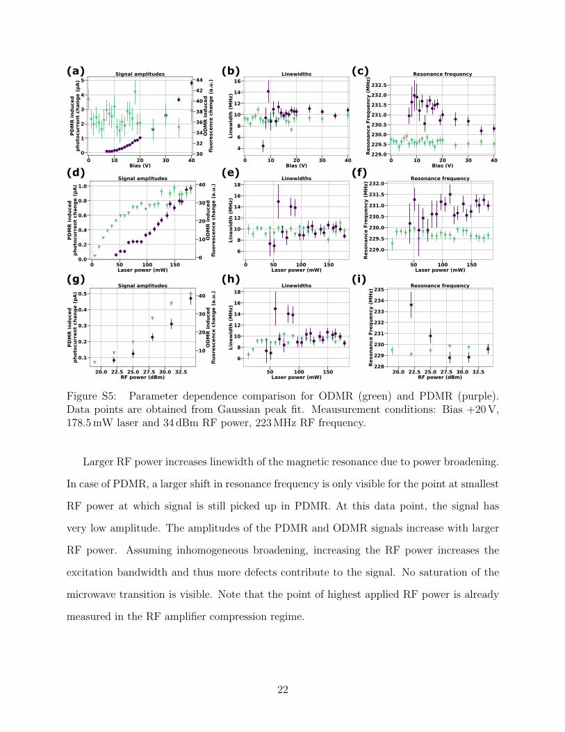
signal. The offset signal is mainly caused by stray RF field. Fig. S5 compares the dependency
of ODMR and PDMR signal, on bases of amplitude, linewidth and resonance frequency
when bias, laser power and RF power are changed. Note that although measurements
have been performed under the same conditions for ODMR and PDMR, a slight offset in
20
detected volume is possible (see discussion in main text). PDMR signals at small laser or
RF powers as well as small bias voltages show low SNR and thus larger errorbars. Errorbars
are obtained from standard error of least-square fitting, neglecting the noise contribution at
each measurement point.
The bias voltage does not affect the ODMR signals. On the other hand, the PDMR
amplitude increases monotonically without saturating. The applied bias determines the
charge extraction efficiency, and larger bias is expected to increase the measured signal
amplitude. Note that linewidth for ODMR and PDMR are similar. A small shift of resonance
frequency dependent on bias is visible for PDMR (see Fig. S5(c)), but not in ODMR. This
shift appears in the low bias regime in which the SNR is poor. At this moment, we do not
have an explanation for this behavior.
The incident laser power does change neither linewidth nor resonance frequency. How-
ever, the fitted peak amplitude increases for both ODMR and PDMR. This observation is
consistent with the suggested mechanism for the PDMR for the V−Si in SiC because stronger
optical excitation will enhance the photo-ionization probability (see Fig. 1(a)-(c) of the main
text). Note that laser power dependence suggests a saturation behaviour for ODMR, while
no saturation could be achieved in the PDMR case.
21
(a) (b) (c)
(d) (e) (f)
(g) (h) (i)
Figure S5: Parameter dependence comparison for ODMR (green) and PDMR (purple).Data points are obtained from Gaussian peak fit. Meausurement conditions: Bias +20 V,178.5 mW laser and 34 dBm RF power, 223 MHz RF frequency.
Larger RF power increases linewidth of the magnetic resonance due to power broadening.
In case of PDMR, a larger shift in resonance frequency is only visible for the point at smallest
RF power at which signal is still picked up in PDMR. At this data point, the signal has
very low amplitude. The amplitudes of the PDMR and ODMR signals increase with larger
RF power. Assuming inhomogeneous broadening, increasing the RF power increases the
excitation bandwidth and thus more defects contribute to the signal. No saturation of the
microwave transition is visible. Note that the point of highest applied RF power is already
measured in the RF amplifier compression regime.
22

Discussion on PDMR contrast, SNR and sensitivity
In a typical ODMR experiment, the contrast c is defined as the spin-dependent fluorescence
change ∆PL at resonance to the off resonance fluorescent signal PLBG (baseline):
c = ∆PL/PLBG. (S1)
As this definition fits the requirement, as long as an absolute signal is acquired, this is not
directly applicable in case of lock-in detection, as only a change in an acquired quantity is
detected. In other words, the absolute measure of the given input is lost, which is essential
for the former definition of contrast, and only changes modulated by the lock-in frequency
are detected. Nevertheless, the detected lock-in signal contains a constant offset. Here,
as the device is in close proximity to the co-planar waveguide, the offset is dominated by
a frequency-dependent coupling of the RF field to the device, which is modulated exactly
at the lock-in frequency. However, the use of this offset in the definition of contrast as
the baseline would lead to a non-physical interpretation of PDMR contrast. Hence, one
could give a device-specific contrast only, which compares the amount of RF coupling for
a given RF frequency with PDMR signal. Based on the original definition of contrast, we
further extend this definition by comparing the amplitude to the maximum acquired signal
as follows:
c = A/max(|BG| , |BG + A|). (S2)
Here, BG is the fluorescence background or dc offset of the PDMR signal and A is the ODMR
or PDMR amplitudes. By this definition, the maximum achievable contrast by fluorescence
is limited to 100%, resulting in a more meaningful quantity. We simultaneously monitor the
detected PDMR signal by lock-in detection and use an oscilloscope in parallel to the lock-in
amplifier in order to detect the mean magnitude of the dc signal. This dc offset additionally
to the previous signals is composed of bias and photocurrent contribution. The lock-in allows
to detect a spin dependent change with maximum sensitivity while the oscilloscope is used
23
to extract the dc offset as a baseline. In particular, we use the oscilloscopes mean value
within a 0.5 s integration window to get the dc offset for each magnetic field point. We
then take the mean value of these points as dc offset. In this recorded data, the PDMR
amplitude is also contained within the data for on-resonance points. As the PDMR and
ODMR amplitudes are very small compared to the dc offset (≈4 orders of magnitude), the
contribution is negligible. The same argument holds for the difference between definitions
in Eq. S1 and Eq. S2. Thus in case of low relative amplitudes, our extended definition of
contrast is comparable to prior work.
Next, we analyze the dependence of contrast and SNR on the experimental conditions.
To correct for differences in measurement time we normalize the SNR to tnorm = 3600 s. The
value for this time-normalized SNRnorm is then calculated by
SNRnorm = SNR√tnorm/tmeas (S3)
where tmeas is the total measurement time and SNR the signal-to-noise ratio calculated by
dividing the fitted amplitude by the obtained standard deviation noise at (see Fig. S7 and
calculation of dc magnetic field sensitivity).
In ODMR measurements, the contrast and SNRnorm do not depend on the bias, while
they do for PDMR as shown in Fig. S6(a) and (b). In PDMR, both contrast and SNRnorm,
are improved for larger bias voltages. We attribute this to a better extraction efficiency of
free electrons and holes in case of PDMR. In terms of contrast a saturating behavior is visible
for larger biases. As can be seen in Fig. S5(a), the amplitude is still increasing, thus the
dc offset must increase more quickly then the signal in this regime. In case of laser power
dependence, we see that ODMR contrast decreases for high laser powers, while the PDMR
contrast still increases (see Fig. S6(c)). The time-normalized SNR shown in Fig. S6(d)
saturates for ODMR, whereas SNR in the PDMR case still increases with laser power. If we
vary the applied RF power, a clear rise in contrast is visible in both measurement techniques,
24

as depicted in Fig. S6(e). SNRnorm is increasing for both PDMR and ODMR with applied RF
power. However, larger RF power leads to larger noise for PDMR due to the RF coupling.
The gain in SNRnorm is thus bigger for ODMR than for PDMR.
(a) (b)
(c) (d)
(e) (f)
Figure S6: DC referred contrast and time-normalized (3600 s) SNR dependent on measure-ment conditions for ODMR (green) and PDMR (purple). Meausurement conditions: Bias+20 V, 178.5 mW laser and 34 dBm RF power, 223 MHz RF frequency.
25

In the following, we calculate the dc magnetic field sensitivity. For this we use the ODMR
and PDMR data shown in Fig. 3(c) in the main text.
The sensitivity is given by comparing the signal power to the noise spectral power. We
estimate the noise by using data points at least 3σ apart from the resonance (see Fig. S7) and
calculating the standard deviation of these data points. This way, we extract a noise level
of 70 fA. Signal-to-noise ratio is then obtained by dividing the PDMR resonance amplitude
by the noise level. The measurement time per point is 25 s for this PDMR measurement,
resulting in a noise spectral density of 350 fA/√
Hz. The slope of the Gaussian peak is
maximum at σ distance, related to the FWHM by FWHM = 2√
2 ln 2σ (see Fig. S7). Thus
the position of the steepest slope can be found by the amplitude and FWHM of the fitted
peak and we find a maximum slope of 1.3 nA/T. From this, we calculate a magnetic field
sensitivity of 253 µT/√
Hz.
For the ODMR, we find a noise level of 290 µV within a measurement time of 2.8 s per
point. With a slope of 21 mV/T we calculate the sensitivity to be 23 µT/√
Hz.
26

Figure S7: Extraction of magnetic field sensitivity and SNR for PDMR. The slope is ex-tracted from the fitted Gaussian at σ distance from the resonance peak. Noise is determinedas standard deviation of measurement points outside of area marked with vertical green lines.
Note that we have not reached the saturation of PDMR signal because of the limitation of
the laser power. Bias and RF power dependence also promise further improvement in SNR
and sensitivity. In addition, while the PDMR contrast is ≈1/10 of the ODMR contrast,
in theory, comparable values might be achievable, as the underlying ISC process is the
same. Thus the SNR, sensitivities and contrast given in the main text and the supporting
information have to be understood as a lower achievable limit.
Local magnetic fields variations inside the device
In order to check for magnetic fields within the device likely introduced by magnetization of
the Ni contacts, we perform ODMR measurements at different depths and x-positions and
extract the resonance frequency. The results are shown in Fig. S8. As the lines can shift a
couple of MHz, magnetic field offsets of a few Gauss appear to be plausible in the device
27

structure. This position-dependent magnetic field might cause the difference in the external
fields between PDMR and ODMR because there might be a slight difference in detection
volume position.
(a) (b)
Figure S8: Magnetic field variation within device. Shift in ODMR resonance peak positiondepending on (a): z-position and (b): x-position.
References
(1) Degen, C.; Reinhard, F.; Cappellaro, P. Quantum sensing. Reviews of Modern Physics
2017, 89 .
(2) Casola, F.; van der Sar, T.; Yacoby, A. Probing condensed matter physics with mag-
netometry based on nitrogen-vacancy centres in diamond. Nature Reviews Materials
2018, 3, 17088.
(3) Atature, M.; Englund, D.; Vamivakas, N.; Lee, S.-Y.; Wrachtrup, J. Material platforms
for spin-based photonic quantum technologies. Nature Reviews Materials 2018, 3, 38–
51.
(4) Yang, S.; Wang, Y.; Rao, D. D. B.; Hien Tran, T.; Momenzadeh, A. S.; Markham, M.;
Twitchen, D. J.; Wang, P.; Yang, W.; Stohr, R.; Neumann, P.; Kosaka, H.;
Wrachtrup, J. High-fidelity transfer and storage of photon states in a single nuclear
spin. Nature Photonics 2016, 10, 507–511.
28

(5) Nagy, R. et al. High-fidelity spin and optical control of single silicon vacancy cen-
tres in silicon carbide. arXiv:1810.10296 [cond-mat, physics:quant-ph] 2018, arXiv:
1810.10296.
(6) Humphreys, P. C.; Kalb, N.; Morits, J. P. J.; Schouten, R. N.; Vermeulen, R. F. L.;
Twitchen, D. J.; Markham, M.; Hanson, R. Deterministic delivery of remote entangle-
ment on a quantum network. Nature 2018, 558, 268–273.
(7) Gruber, A. Scanning Confocal Optical Microscopy and Magnetic Resonance on Single
Defect Centers. Science 1997, 276, 2012–2014.
(8) Jelezko, F.; Gaebel, T.; Popa, I.; Gruber, A.; Wrachtrup, J. Observation of Coherent
Oscillations in a Single Electron Spin. Physical Review Letters 2004, 92 .
(9) Widmann, M. et al. Coherent control of single spins in silicon carbide at room temper-
ature. Nature Materials 2015, 14, 164–168.
(10) Christle, D. J.; Falk, A. L.; Andrich, P.; Klimov, P. V.; Hassan, J. U.; Son, N. T.;
Janzen, E.; Ohshima, T.; Awschalom, D. D. Isolated electron spins in silicon carbide
with millisecond coherence times. Nature Materials 2015, 14, 160–163.
(11) Morello, A. et al. Single-shot readout of an electron spin in silicon. Nature 2010, 467,
687–691.
(12) Morton, J. J. L.; McCamey, D. R.; Eriksson, M. A.; Lyon, S. A. Embracing the quantum
limit in silicon computing. Nature 2011, 479, 345–353.
(13) Zwanenburg, F. A.; Dzurak, A. S.; Morello, A.; Simmons, M. Y.; Hollenberg, L. C. L.;
Klimeck, G.; Rogge, S.; Coppersmith, S. N.; Eriksson, M. A. Silicon quantum electron-
ics. Reviews of Modern Physics 2013, 85, 961–1019.
(14) Hanson, R.; van Beveren, L. H. W.; Vink, I. T.; Elzerman, J. M.; Naber, W. J. M.;
Koppens, F. H. L.; Kouwenhoven, L. P.; Vandersypen, L. M. K. Single-Shot Readout of
29

Electron Spin States in a Quantum Dot Using Spin-Dependent Tunnel Rates. Physical
Review Letters 2005, 94 .
(15) Godfrin, C.; Thiele, S.; Ferhat, A.; Klyatskaya, S.; Ruben, M.; Wernsdorfer, W.; Bale-
stro, F. Electrical Read-Out of a Single Spin Using an Exchange-Coupled Quantum
Dot. ACS Nano 2017, 11, 3984–3989.
(16) van Tol, J.; Morley, G. W.; Takahashi, S.; McCamey, D. R.; Boehme, C.; Zvanut, M. E.
High-Field Phenomena of Qubits. Applied Magnetic Resonance 2009, 36, 259–268.
(17) Waldherr, G.; Beck, J.; Steiner, M.; Neumann, P.; Gali, A.; Frauenheim, T.; Jelezko, F.;
Wrachtrup, J. Dark States of Single Nitrogen-Vacancy Centers in Diamond Unraveled
by Single Shot NMR. Physical Review Letters 2011, 106 .
(18) Tetienne, J.-P.; Rondin, L.; Spinicelli, P.; Chipaux, M.; Debuisschert, T.; Roch, J.-F.;
Jacques, V. Magnetic-field-dependent photodynamics of single NV defects in diamond:
an application to qualitative all-optical magnetic imaging. New Journal of Physics
2012, 14, 103033.
(19) Stegner, A. R.; Boehme, C.; Huebl, H.; Stutzmann, M.; Lips, K.; Brandt, M. S. Electri-
cal detection of coherent 31P spin quantum states. Nature Physics 2006, 2, 835–838.
(20) McCamey, D. R.; Seipel, H. A.; Paik, S.-Y.; Walter, M. J.; Borys, N. J.; Lupton, J. M.;
Boehme, C. Spin Rabi flopping in the photocurrent of a polymer light-emitting diode.
Nature Materials 2008, 7, 723–728.
(21) Franke, D. P.; Hoehne, F.; Vlasenko, L. S.; Itoh, K. M.; Brandt, M. S. Spin-dependent
recombination involving oxygen-vacancy complexes in silicon. Physical Review B 2014,
89 .
(22) Lee, S.-Y.; Paik, S.-Y.; McCamey, D. R.; Hu, J.; Zhu, F.; Madan, A.; Boehme, C. Spin-
30
dependent processes in amorphous silicon-rich silicon-nitride. Applied Physics Letters
2010, 97, 192104.
(23) Bourgeois, E.; Jarmola, A.; Siyushev, P.; Gulka, M.; Hruby, J.; Jelezko, F.; Budker, D.;
Nesladek, M. Photoelectric detection of electron spin resonance of nitrogen-vacancy
centres in diamond. Nature Communications 2015, 6 .
(24) Hrubesch, F. M.; Braunbeck, G.; Stutzmann, M.; Reinhard, F.; Brandt, M. S. Efficient
Electrical Spin Readout of NV - Centers in Diamond. Physical Review Letters 2017,
118 .
(25) Siyushev, P.; Nesladek, M.; Bourgeois, E.; Gulka, M.; Hruby, J.; Yamamoto, T.;
Trupke, M.; Teraji, T.; Isoya, J.; Jelezko, F. Photoelectrical imaging and coherent
spin-state readout of single nitrogen-vacancy centers in diamond. Science 2019, 363,
728–731.
(26) Kimoto, T.; Cooper, J. A. Fundamentals of silicon carbide technology: growth, charac-
terizaton, devices and applications ; Wiley [u.a.]: Singapore, 2014; OCLC: 879610937.
(27) Isoya, J.; Umeda, T.; Mizuochi, N.; Son, N. T.; Janzen, E.; Ohshima, T. EPR Iden-
tification of Defects and Impurities in SiC: To be Decisive. Materials Science Forum
2008, 600-603, 279–284.
(28) Mizuochi, N.; Yamasaki, S.; Takizawa, H.; Morishita, N.; Ohshima, T.; Itoh, H.;
Isoya, J. Continuous-wave and pulsed EPR study of the negatively charged silicon
vacancy with S = 3 2 and C 3 v symmetry in n -type 4 H - SiC. Physical Review B
2002, 66 .
(29) Cochrane, C. J.; Bittel, B. C.; Lenahan, P. M.; Fronheiser, J.; Matocha, K.; Lelis, A. J.
EDMR and EPR Studies of 4H SiC MOSFETs and Capacitors. Materials Science Fo-
rum 2010, 645-648, 527–530.
31

(30) Sato, T.; Yokoyama, H.; Ohya, H. Electrically Detected Magnetic Resonance (EDMR)
Measurements of Bulk Silicon Carbide (SiC) Crystals. Chemistry Letters 2006, 35,
1428–1429.
(31) Gruber, G.; Cottom, J.; Meszaros, R.; Koch, M.; Pobegen, G.; Aichinger, T.; Peters, D.;
Hadley, P. Electrically detected magnetic resonance of carbon dangling bonds at the
Si-face 4H-SiC/SiO 2 interface. Journal of Applied Physics 2018, 123, 161514.
(32) Umeda, T.; Kosugi, R.; Fukuda, K.; Morishita, N.; Ohshima, T.; Esaki, K.; Isoya, J.
Electrically Detected Magnetic Resonance (EDMR) Studies of SiC-SiO2 Interfaces. Ma-
terials Science Forum 2012, 717-720, 427–432.
(33) Cottom, J.; Gruber, G.; Hadley, P.; Koch, M.; Pobegen, G.; Aichinger, T.; Shluger, A.
Recombination centers in 4H-SiC investigated by electrically detected magnetic reso-
nance and ab initio modeling. Journal of Applied Physics 2016, 119, 181507.
(34) Cochrane, C. J.; Blacksberg, J.; Anders, M. A.; Lenahan, P. M. Vectorized magne-
tometer for space applications using electrical readout of atomic scale defects in silicon
carbide. Scientific Reports 2016, 6 .
(35) Simin, D.; Kraus, H.; Sperlich, A.; Ohshima, T.; Astakhov, G. V.; Dyakonov, V. Lock-
ing of electron spin coherence above 20 ms in natural silicon carbide. Physical Review
B 2017, 95 .
(36) Carter, S. G.; Soykal, . O.; Dev, P.; Economou, S. E.; Glaser, E. R. Spin coherence
and echo modulation of the silicon vacancy in 4 H - SiC at room temperature. Physical
Review B 2015, 92 .
(37) Simin, D.; Fuchs, F.; Kraus, H.; Sperlich, A.; Baranov, P.; Astakhov, G.; Dyakonov, V.
High-Precision Angle-Resolved Magnetometry with Uniaxial Quantum Centers in Sili-
con Carbide. Physical Review Applied 2015, 4 .
32

(38) Simin, D.; Soltamov, V.; Poshakinskiy, A.; Anisimov, A.; Babunts, R.; Tolmachev, D.;
Mokhov, E.; Trupke, M.; Tarasenko, S.; Sperlich, A.; Baranov, P.; Dyakonov, V.; As-
takhov, G. All-Optical dc Nanotesla Magnetometry Using Silicon Vacancy Fine Struc-
ture in Isotopically Purified Silicon Carbide. Physical Review X 2016, 6 .
(39) Niethammer, M.; Widmann, M.; Lee, S.-Y.; Stenberg, P.; Kordina, O.; Ohshima, T.;
Son, N. T.; Janzen, E.; Wrachtrup, J. Vector Magnetometry Using Silicon Vacancies in
4 H -SiC Under Ambient Conditions. Physical Review Applied 2016, 6 .
(40) Anisimov, A. N.; Simin, D.; Soltamov, V. A.; Lebedev, S. P.; Baranov, P. G.; As-
takhov, G. V.; Dyakonov, V. Optical thermometry based on level anticrossing in silicon
carbide. Scientific Reports 2016, 6 .
(41) Wimbauer, T.; Meyer, B. K.; Hofstaetter, A.; Scharmann, A.; Overhof, H. Negatively
charged Si vacancy in 4 H SiC: A comparison between theory and experiment. Physical
Review B 1997, 56, 7384–7388.
(42) Sorman, E.; Son, N. T.; Chen, W. M.; Kordina, O.; Hallin, C.; Janzen, E. Silicon
vacancy related defect in 4H and 6H SiC. Physical Review B 2000, 61, 2613–2620.
(43) Tarasenko, S. A.; Poshakinskiy, A. V.; Simin, D.; Soltamov, V. A.; Mokhov, E. N.;
Baranov, P. G.; Dyakonov, V.; Astakhov, G. V. Spin and Optical Properties of Silicon
Vacancies in Silicon Carbide - A Review. physica status solidi (b) 2018, 255, 1700258.
(44) Kraus, H.; Soltamov, V. A.; Riedel, D.; Vath, S.; Fuchs, F.; Sperlich, A.; Baranov, P. G.;
Dyakonov, V.; Astakhov, G. V. Room-temperature quantum microwave emitters based
on spin defects in silicon carbide. Nature Physics 2014, 10, 157–162.
(45) Yang, L.-P.; Burk, C.; Widmann, M.; Lee, S.-Y.; Wrachtrup, J.; Zhao, N. Electron spin
decoherence in silicon carbide nuclear spin bath. Physical Review B 2014, 90 .
33
(46) Ohyama, H.; Takakura, K.; Watanabe, T.; Nishiyama, K.; Shigaki, K.; Kudou, T.;
Nakabayashi, M.; Kuboyama, S.; Matsuda, S.; Kamezawa, C.; Simoen, E.; Claey, C.
Radiation damage of SiC Schottky diodes by electron irradiation. Journal of Materials
Science: Materials in Electronics 2005, 16, 455–458.
(47) Magnusson, B.; Son, N. T.; Csore, A.; Gallstrom, A.; Ohshima, T.; Gali, A.;
Ivanov, I. G. Excitation properties of the divacancy in 4H -SiC. Physical Review B
2018, 98 .
(48) Aslam, N.; Waldherr, G.; Neumann, P.; Jelezko, F.; Wrachtrup, J. Photo-induced ion-
ization dynamics of the nitrogen vacancy defect in diamond investigated by single-shot
charge state detection. New Journal of Physics 2013, 15, 013064.
(49) Siyushev, P.; Pinto, H.; Voros, M.; Gali, A.; Jelezko, F.; Wrachtrup, J. Optically Con-
trolled Switching of the Charge State of a Single Nitrogen-Vacancy Center in Diamond
at Cryogenic Temperatures. Physical Review Letters 2013, 110 .
(50) Schirhagl, R.; Chang, K.; Loretz, M.; Degen, C. L. Nitrogen-Vacancy Centers in Dia-
mond: Nanoscale Sensors for Physics and Biology. Annual Review of Physical Chemistry
2014, 65, 83–105.
(51) Taylor, J. M.; Cappellaro, P.; Childress, L.; Jiang, L.; Budker, D.; Hemmer, P. R.;
Yacoby, A.; Walsworth, R.; Lukin, M. D. High-sensitivity diamond magnetometer with
nanoscale resolution. Nature Physics 2008, 4, 810–816.
(52) Djekic, D.; Fantner, G.; Lips, K.; Ortmanns, M.; Anders, J. A 0.1% THD, 1-M Ω to
1-G Ω Tunable, Temperature-Compensated Transimpedance Amplifier Using a Multi-
Element Pseudo-Resistor. IEEE Journal of Solid-State Circuits 2018, 53, 1913–1923.
(53) Lu, W.; Ou, Y.; Fiordaliso, E. M.; Iwasa, Y.; Jokubavicius, V.; Syvajarvi, M.;
Kamiyama, S.; Petersen, P. M.; Ou, H. White Light Emission from Fluorescent SiC
with Porous Surface. Scientific Reports 2017, 7 .
34


![Theory and Application to YbMgGaO - arXivtom]: RG ows at low energies can produce longer-range ran-dom singlets, larger-spin clusters and spin glass freezing of the nucleated spins.](https://static.fdocuments.in/doc/165x107/5fefe0d66b9668392a795caf/theory-and-application-to-ybmggao-arxiv-tom-rg-ows-at-low-energies-can-produce.jpg)


