CN310 Microprocessor Systems Design · An Analog-to-Digital converter (ADC) is an electronic device...
28
CN310 Microprocessor Systems Design Analogue Signals Nawin Somyat Department of Electrical and Computer Engineering Thammasat University
Transcript of CN310 Microprocessor Systems Design · An Analog-to-Digital converter (ADC) is an electronic device...

CN310 Microprocessor Systems DesignAnalogue Signals
Nawin Somyat
Department of Electrical and Computer EngineeringThammasat University
Outline
Course Contents1 Introduction2 Simple Computer3 Microprocessor Architecture4 Memory5 Peripherals6 Applications
Outline1 Introduction2 ADC
Flash ADCDigital Ramp ADCSuccessiveApproximation ADC
CN310 Microprocessor Systems Design 2 / 28

Analogue Signals
Signals are set of values that convey information and can bemeasured by any independent attribute such as time or space, e.g.sound over time, sound over distance.Two classes of signals:
Analogue signals - continuousDigital signals - discrete
Physical domain contains analogue signals.In digital domain, analogue signals have to be converted to digitalsignals before processing.
CN310 Microprocessor Systems Design 3 / 28

Analogue to Digital Conversion
CN310 Microprocessor Systems Design 4 / 28

Analogue to Digital Conversion
Since:analogue signals are continuousconversion may take some finite time
Analogue signals are normally sampled at a suitable rate.The rate at which the signals are sampled is called sampling rate.Normal unit for sampling rate is “samples per second”.From “Sampling theorem”:
a band limited analogue signal that has been sampledcan be perfectly reconstructed from an infinite sequence ofsamples if
the sampling rate exceeds 2B samples per secondwhere B is the highest frequency of the original signal
CN310 Microprocessor Systems Design 5 / 28

Analogue to Digital Conversion
For an analogue signal:there is possibly an infinite range of values.each sampled signal has to be converted into a finite set ofvalues.
“Quantization”:the process of converting signals into values in a finite set ofvalues.each value in the set is known as “Quantization Levels”.difference between actual analogue value and thequantized/digitize value is known as “Quantization Error”, or“Quantization Distortion”.
CN310 Microprocessor Systems Design 6 / 28

Analogue to Digital Conversion
Since digitized signal are commonly encoded into binary number,the number of quatization level depends on the number of bits usein a binary number.“Resolution”
the number of bits used to store each sampled signal.electrically, this resolution is expressed in volts
For example, an 8-bit resolution means a sampled and digitizedsignal is stored as an 8-bit number. This number can represent 1of 256 (28) possible values.Voltage resolution of conversion is equal to voltage measurementrange divided by the number of quantization levels.
Q =EFSR
N =ERefHi − ERefLo
2M
where M is the number of bits.CN310 Microprocessor Systems Design 7 / 28

Analogue to Digital Conversion: Example
Example: 10.1Consider a 10-bit analogue-to-digital conversion with range 0 - 5V:
Maximum Voltage: ERefHi = 5 Volts
Minimum Voltage: ERefLo = 0 Volts
Full scale range (FSR) = ERefHi − ERefLo = 5V - 0V = 5V
Resolution (N) => 10 bits => 210 = 1024 levels
Voltage resolution (Q) = EFSRN = 5
1024 = 0.00488V = 4.88 mV
CN310 Microprocessor Systems Design 8 / 28

Analogue-to-Digital Converter
An Analog-to-Digital converter (ADC) is an electronic devicewhich converts analogue signals to digtal sinals suitable for digitalprocessing.This means that input to an ADC must be properly conditionedelectrical signal.Common ADC types:
direct conversion ADC (flash ADC)delta-encoded ADC (counter or digital ramp ADC)successive approximation ADCsigma-delta ADC (delta-sigma ADC)pipeline ADCintegrating ADC (dual-slope or multi-slope ADC)
CN310 Microprocessor Systems Design 9 / 28
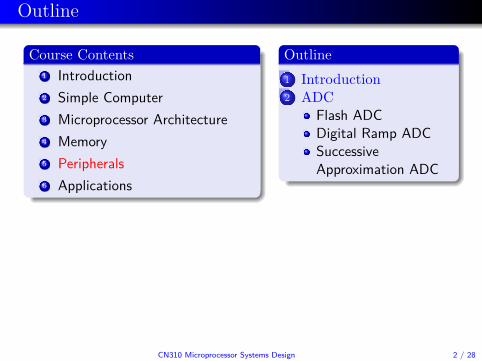
ADCs
ADC architectures, resolution and sampling rates.CN310 Microprocessor Systems Design 10 / 28

Flash ADC
Fastest conversion timeused in digital scopes, video sampling, etc.
Good for only a few bits of resolutiondifificult to get high accuracy at higher resolution
CN310 Microprocessor Systems Design 11 / 28

Flash ADC: Example
ful scale volatage range = 5 - 0 = 5 Vanalogue input is 3 Vresolution = 2 bitsresult: Y1Y0 = 10 indicates input is in the range 2.25 - 3.75 V
CN310 Microprocessor Systems Design 12 / 28

Digital Ramp ADC (Counter)
CN310 Microprocessor Systems Design 13 / 28

Digital Ramp ADC (Counter)
This simple ADC uses a binary counter as counter register.A START pulse resets the counter and disables the ANDgate.With all 0s at its input, the DAC’s output is Vdac = 0 V.Since Vdac < Vin_a, the EOC output will be HIGH.When START returns to LOW, the AND gate is enabled.As the counter advances, the DAC output, Vdac, increasesone step at a time.This continues until Vdac reaches a step that just exceedsVin_a by about 1 voltage resolution.EOC then becomes LOW, disabling the AND gate.The conversion is now complete and the contents of thecounter register are the digital representation of Vin_a.The digital data is lost at the next START pulse.
CN310 Microprocessor Systems Design 14 / 28

Successive Approximation ADC
CN310 Microprocessor Systems Design 15 / 28

Successive Approximation ADC
A START pulse clears all the bits and disables the CLU.Conversion begins with the MSb = 1.If Vin_a < Vdac, then clear the last set bit back to 0.If all bits have been checked then proceed, otherwise repeatby setting the next lower significant bit to a 1.After all bits have been checked, EOC = 1.The conversion is now complete and the contents of theregister are the digital representation of Vin_a.The digital data is lost at the next START pulse unlessstored in some sort of memory device or location.
CN310 Microprocessor Systems Design 16 / 28

ADC Specification
Resolution - in bitsAccuracy - in % of full scale Vref or number of LSbsConversion time - seconds (e.g. µs)Sampling rate - samples per second
CN310 Microprocessor Systems Design 17 / 28

ATMega168 - ADC
Features:10-bit Resolution0.5 LSB Integral Non-linearity± 2 LSB Absolute Accuracy13 - 260 µs Conversion TimeUp to 76.9 kSPS (Up to 15 kSPS at Maximum Resolution)6 Multiplexed Single Ended Input Channels2 Additional Multiplexed Single Ended Input Channels (TQFPand QFN/MLF Package only)Temperature Sensor Input ChannelOptional Left Adjustment for ADC Result Readout0 - VCC ADC Input Voltage RangeSelectable 1.1V ADC Reference VoltageFree Running or Single Conversion ModeInterrupt on ADC Conversion CompleteSleep Mode Noise Canceler
CN310 Microprocessor Systems Design 18 / 28

ATMega168 - ADC block Diagram
CN310 Microprocessor Systems Design 19 / 28

ATMega168 - ADC Timing Diagram: First Conversion
In Single Conversion Mode, the first conversion after the ADC isswitched on (ADEN in ADCSRA is set) takes 25 ADC clock cyclesin order to initialise the analogue circuitry.
CN310 Microprocessor Systems Design 20 / 28

ATMega168 - ADC Timing Diagram: Next Conversion
In Single Conversion Mode, a normal conversion takes 13 ADCclock cycles.
CN310 Microprocessor Systems Design 21 / 28

ATMega168 - ADC Prescaler
By default, the successive approximation circuitry requires an inputclock frequency between 50kHz and 200kHz to get maximumresolution. If a lower resolution than 10 bits is needed, the inputclock frequency to the ADC can be higher than 200kHz to get ahigher sample rate.The ADC module contains a prescaler, which generates anacceptable ADC clock frequency from any CPU frequency above100kHz. The prescaling is set by the ADPS bits in ADCSRA.
CN310 Microprocessor Systems Design 22 / 28
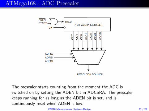
ATMega168 - ADC Prescaler
The prescaler starts counting from the moment the ADC isswitched on by setting the ADEN bit in ADCSRA. The prescalerkeeps running for as long as the ADEN bit is set, and iscontinuously reset when ADEN is low.
CN310 Microprocessor Systems Design 23 / 28

ATMega168 - ADC Registers
CN310 Microprocessor Systems Design 24 / 28
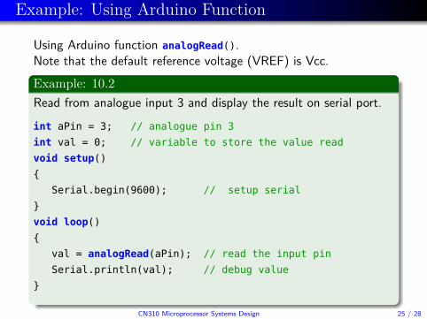
Example: Using Arduino Function
Using Arduino function analogRead().Note that the default reference voltage (VREF) is Vcc.Example: 10.2Read from analogue input 3 and display the result on serial port.int aPin = 3; // analogue pin 3int val = 0; // variable to store the value readvoid setup(){
Serial.begin(9600); // setup serial}void loop(){
val = analogRead(aPin); // read the input pinSerial.println(val); // debug value
}
CN310 Microprocessor Systems Design 25 / 28

Example: Using I/O Registers
Example: 10.3Read from analogue input 3 and display the result on serial port.int val = 0; // variable to store the value readvoid setup(){
// Set reference voltage.// Set values for REFS1:0 to 01// This selects AVCC with external capacitor at AREF pinADMUX |= (1<<REFS0);ADMUX &= ~(1<<REFS1);// MUX3:0 = 0011 to select analogue input channel 3ADMUX |= (1<<MUX1) | (1<<MUX0);ADMUX &= ~( (1<<MUX3) | (1<<MUX2) );// Select prescaler to 128, ADPS2:0 = 111// For 16MHz system clock, this gives ADC clock of 125kHzADCSRA |= (1<<ADPS2) | (1<<ADPS1) | (1<<ADPS0);
CN310 Microprocessor Systems Design 26 / 28

Example: Using I/O Registers
Example: 10.3
ADCSRA |= (1<<ADEN); // enable ADCSerial.begin(9600); // setup serial
}void loop(){
ADCSRA |= (1<<ADSC); // start conversion// wait until conversion completes, i.e. when ADSC == 0while ( ADCSRA & (1<<ADSC) );// if ADLAR == 0, ADCH contains the upper 2 bitsval = ADCL; // must read low byte firstval |= (ADCH<<8); // then read high byteSerial.println(val); // debug value
}
CN310 Microprocessor Systems Design 27 / 28

Example
From previous example:If the value read is, for example, 678, Vcc = 5V:The actual analogue voltage is:
Vin = ADC × VREF210 − 1 = 678 × 5
1023 = 3.313782991V
CN310 Microprocessor Systems Design 28 / 28