cn.mouser.comcn.mouser.com/datasheet/2/268/PIC16(L)F1764-5-8-9-14-20...2018-03-242014-2018 Microchip...
564
2014-2018 Microchip Technology Inc. DS40001775D-page 1 PIC16(L)F1764/5/8/9 Description The PIC16(L)F1764/5/8/9 family offers intelligent analog with digital peripherals to create up to two independent closed- loop channels. These 14 and 20-pin devices enable the ability to interconnect the on-chip peripherals to create custom functions specific to each application; helping simplify the implementation of a complex control system and give designers the flexibility to innovate. Core Features • C Compiler Optimized RISC Architecture • Only 49 Instructions • Operating Speed: - DC – 32 MHz clock input - 125 ns minimum instruction cycle • Interrupt Capability • 16-Level Deep Hardware Stack • Up to Four 8-Bit Timers • Up to Three 16-Bit Timers • Power-on Reset (POR) • Configurable Power-up Timer (PWRT) • Brown-out Reset (BOR) with Selectable Trip Point • Extended Watchdog Timer (EWDT): - Low-power 31 kHz WDT - Software-selectable prescaler - Software-selectable enable Memory • Up to 14 Kbytes Flash Program Memory • Up to 1024 Bytes Data RAM Memory • Direct, Indirect and Relative Addressing modes • High-Endurance Flash (HEF): - 128B of nonvolatile data storage - 100K erase/write cycles Operating Characteristics • Operating Voltage Range: - 1.8V to 3.6V (PIC16LF1764/5/8/9) - 2.3V to 5.5V (PIC16F1764/5/8/9) • Temperature Range: - Industrial: -40°C to +85°C - Extended: -40°C to +125°C eXtreme Low-Power (XLP) Features • Sleep mode: 50 nA @ 1.8V, typical • Watchdog Timer: 500 nA @ 1.8V, typical • Secondary Oscillator: 500 nA @ 32 kHz • Operating Current: -8 A @ 32 kHz, 1.8V, typical - 32 A/MHz @ 1.8V, typical • Low-Power BOR (LPBOR): - 200 nA in Sleep Digital Peripherals • Configurable Logic Cell (CLC): - Up to three CLCs; up to four selected inputs - Integrated combinational and state logic • Up to Two Complementary Output Generators (COG): - Push-Pull, Full-Bridge and Steering modes • Up to Two Capture/Compare/PWM (CCP) modules • Pulse-Width Modulators (PWM): - Up to two 10-bit PWMs - Up to two 16-bit PWMs • Peripheral Pin Select (PPS): - Configure any digital pin to output • Serial Communications: - Enhanced USART (EUSART) - SPI, I 2 C, RS-232, RS-485, LIN compatible - Auto-Baud Detect, auto-wake-up on start • Up to 18 I/O Pins: - Individually programmable pull-ups - Slew rate control - Interrupt-On-Change (IOC) with edge select • Up to Two Data Signal Modulators (DSM) Intelligent Analog Peripherals • 10-Bit Analog-to-Digital Converter (ADC): - Up to 12 external channels - Conversion available during Sleep • Up to Two Operational Amplifiers (OPA): - Selectable internal and external channels • Up to Four Fast Comparators (COMP): - Up to five external inverting inputs - Up to eight external non-inverting inputs - Fixed Voltage Reference at non-inverting input(s) - Comparator outputs externally accessible • Digital-to-Analog Converters (DAC): - Up to two 10-bit resolution DACs - Up to two 5-bit resolution DACs 14/20-Pin, 8-Bit Flash Microcontrollers
Transcript of cn.mouser.comcn.mouser.com/datasheet/2/268/PIC16(L)F1764-5-8-9-14-20...2018-03-242014-2018 Microchip...

2014-2018 Microchip Technology Inc. DS40001775D-page 1
PIC16(L)F1764/5/8/9
Description
The PIC16(L)F1764/5/8/9 family offers intelligent analog with digital peripherals to create up to two independent closed-loop channels. These 14 and 20-pin devices enable the ability to interconnect the on-chip peripherals to create customfunctions specific to each application; helping simplify the implementation of a complex control system and givedesigners the flexibility to innovate.
Core Features
• C Compiler Optimized RISC Architecture• Only 49 Instructions• Operating Speed:
- DC – 32 MHz clock input- 125 ns minimum instruction cycle
• Interrupt Capability• 16-Level Deep Hardware Stack• Up to Four 8-Bit Timers• Up to Three 16-Bit Timers• Power-on Reset (POR)• Configurable Power-up Timer (PWRT)• Brown-out Reset (BOR) with Selectable Trip Point• Extended Watchdog Timer (EWDT):
- Low-power 31 kHz WDT - Software-selectable prescaler- Software-selectable enable
Memory
• Up to 14 Kbytes Flash Program Memory• Up to 1024 Bytes Data RAM Memory• Direct, Indirect and Relative Addressing modes• High-Endurance Flash (HEF):
- 128B of nonvolatile data storage- 100K erase/write cycles
Operating Characteristics• Operating Voltage Range:
- 1.8V to 3.6V (PIC16LF1764/5/8/9)- 2.3V to 5.5V (PIC16F1764/5/8/9)
• Temperature Range:- Industrial: -40°C to +85°C- Extended: -40°C to +125°C
eXtreme Low-Power (XLP) Features
• Sleep mode: 50 nA @ 1.8V, typical • Watchdog Timer: 500 nA @ 1.8V, typical • Secondary Oscillator: 500 nA @ 32 kHz • Operating Current:
- 8 A @ 32 kHz, 1.8V, typical - 32 A/MHz @ 1.8V, typical
• Low-Power BOR (LPBOR):- 200 nA in Sleep
Digital Peripherals
• Configurable Logic Cell (CLC): - Up to three CLCs; up to four selected inputs- Integrated combinational and state logic
• Up to Two Complementary Output Generators (COG):
- Push-Pull, Full-Bridge and Steering modes• Up to Two Capture/Compare/PWM (CCP)
modules• Pulse-Width Modulators (PWM):
- Up to two 10-bit PWMs- Up to two 16-bit PWMs
• Peripheral Pin Select (PPS):- Configure any digital pin to output
• Serial Communications:- Enhanced USART (EUSART)- SPI, I2C, RS-232, RS-485, LIN compatible- Auto-Baud Detect, auto-wake-up on start
• Up to 18 I/O Pins:- Individually programmable pull-ups - Slew rate control - Interrupt-On-Change (IOC) with edge select
• Up to Two Data Signal Modulators (DSM)
Intelligent Analog Peripherals
• 10-Bit Analog-to-Digital Converter (ADC):- Up to 12 external channels- Conversion available during Sleep
• Up to Two Operational Amplifiers (OPA):- Selectable internal and external channels
• Up to Four Fast Comparators (COMP):- Up to five external inverting inputs- Up to eight external non-inverting inputs- Fixed Voltage Reference at non-inverting
input(s) - Comparator outputs externally accessible
• Digital-to-Analog Converters (DAC):- Up to two 10-bit resolution DACs- Up to two 5-bit resolution DACs
14/20-Pin, 8-Bit Flash Microcontrollers

2014-2018 Microchip Technology Inc. DS40001775D-page 2
PIC16(L)F1764/5/8/9
Intelligent Analog Peripherals (Cont.)
• Voltage Reference: - Fixed Voltage Reference (FVR): 1.024V,
2.048V and 4.096V output levels• Zero-Cross Detector (ZCD):
- Detect high-voltage AC signal • Programmable Ramp Generator (PRG):
- Slope compensation - Ramp generation
• High-Current Drive I/Os:- 100 mA capacity @ 5V
Clocking Structure
• 16 MHz Internal Oscillator:- ±1% at calibration- Selectable frequency range, 32 MHz to
31 kHz• 31 kHz Low-Power Internal Oscillator• 4x Phase-Locked Loop (PLL):
- For up to 32 MHz internal operation• External Oscillator Block with:
- Three External Clock modes up to 32 MHz
TABLE 1: PIC16(L)F1764/5/8/9 FAMILY TYPES
Device
Da
ta S
hee
t In
de
x
Pro
gra
m M
emo
ry F
lash
(Wo
rds/
Kb
yte
s)
Hig
h-E
nd
ura
nc
e F
las
h (
B)
Da
ta S
RA
M (
Byt
es
)
I/O P
ins(2
)
16
-Bit
Tim
ers
8-B
it T
imer
s w
/HLT
Co
mp
arat
or
10-B
it A
DC
(c
h)
5/1
0-B
it D
AC
CC
P
10
/16
-Bit
PW
M
CO
G
Da
ta S
ign
al M
od
ula
tor
CL
C
Op
Am
p
Ze
ro-C
ross
De
tect
Pro
gra
mm
ab
le R
amp
Ge
n
Hig
h-C
urr
ent
I/Os
Per
iph
era
l P
in S
ele
ct
EU
SA
RT
I2C
/SP
I
De
bu
g(1
)
PIC16(L)F1764 (A) 4096/7 128 512 12 3 1/3 2 8 1/1 1 1/1 1 1 3 1 1 1 2 Y 1 1 I/H
PIC16(L)F1765 (A) 8192/14 128 1024 12 3 1/3 2 8 1/1 1 1/1 1 1 3 1 1 1 2 Y 1 1 I/H
PIC16(L)F1768 (A) 4096/7 128 512 18 3 1/3 4 12 2/2 2 2/2 2 2 3 2 1 2 2 Y 1 1 I/H
PIC16(L)F1769 (A) 8192/14 128 1024 18 3 1/3 4 12 2/2 2 2/2 2 2 3 2 1 2 2 Y 1 1 I/H
Note 1: Debugging Methods: (I) – Integrated on Chip; (H) – via ICD Header; E – Emulation Product.
2: One pin is input-only.
Data Sheet Index: (Unshaded devices are described in this document.)
A. DS-40001775 PIC16(L)F1764/5/8/9 Data Sheet, 14/20-Pin 8-Bit Flash Microcontrollers.
Note: For other small form factor package availability and marking information, please visithttp://www.microchip.com/packaging or contact your local sales office.
TABLE 2: PACKAGES
Packages PDIP SOIC TSSOP QFN SSOP
PIC16(L)F1764 PIC16(L)F1765 PIC16(L)F1768 PIC16(L)F1769
Note: Pin details are subject to change.
2014-2018 Microchip Technology Inc. DS40001775D-page 3
PIC16(L)F1764/5/8/9
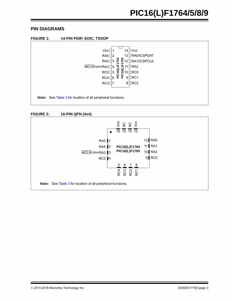
PIN DIAGRAMS
FIGURE 1: 14-PIN PDIP, SOIC, TSSOP
FIGURE 2: 16-PIN QFN (4x4)
VDD
RA5
RA4
MCLR/VPP/RA3
RC5
RC4
VSS
RA0/ICSPDAT
RA1/ICSPCLK
RA2
RC0
RC1
RC2RC3
Note: See Table 3 for location of all peripheral functions.
PIC
16
(L)F
17
64
PIC
16
(L)F
17
65
1
2
3
4
14
13
12
11
5
6
7
10
9
8
PIC16(L)F1764PIC16(L)F1765
RA0
RA1
RA2
RC09
10
11
12
5 6
RC
4
RC
3
RC
1
RC
2
7 8
2
3
1
4
RA5
RA4
MCLR/VPP/RA3
RC5
1516 1314
NC
VD
D
NC
VS
S
Note: See Table 3 for location of all peripheral functions.

2014-2018 Microchip Technology Inc. DS40001775D-page 4
PIC16(L)F1764/5/8/9
FIGURE 3: 20-PIN PDIP, SOIC, SSOP
FIGURE 4: 20-PIN QFN (4x4)P
IC1
6(L
)F1
768
PIC
16
(L)F
176
9
1
2
3
4
14
13
12
11
5
6
7
10
9
8
VDD
RA5
RA4
MCLR/VPP/RA3
RC5
RC4
VSS
RA0
RA1
RA2
RC0
RC1
RC2RC3
Note: See Table 4 for location of all peripheral functions.
18
17
16
15
20
19
RC6
RC7
RB7
RB4
RB5
RB6
PIC16(L)F1768
PIC16(L)F1769
Note: See Table 4 for location of all peripheral functions.
15 RA1
RA2
RC0
RC1
RC211
12
13
14
6 7
RC
7
RB
7
RB
4
RB
5
RB
6
8 9 10
2
3
1
181920 1617
5
4
VD
D
RA
5
RA
4
MCLR/VPP/RA3
RC5
RC4
RC3
RC6
VS
S
RA
0

2
01
4-2
01
8 M
icroch
ip T
ech
no
log
y Inc.
DS
40
00
17
75
D-p
ag
e 5
PIC
16(L)F
1764/5/8/9
PIN ALLOCATION TABLES
TABLE 3: 14-PIN AND 16-PIN ALLOCATION TABLE (PIC16(L)F1764/5)
I/O
14-
Pin
PD
IP/S
OIC
/TS
SO
P
16
-Pin
QF
N
AD
C
Re
fere
nc
e
DA
C
Op
Am
p
Co
mp
ara
tor
Ze
ro C
ros
s
Pro
gra
mm
able
Ra
mp
Gen
era
tor
Tim
ers
PW
M
CC
P
CO
G
CL
C
Mo
du
lato
r
EU
SA
RT
MS
SP
Inte
rru
pts
Pu
ll-u
ps
Hi C
urr
en
t
Ba
sic
RA0 13 12 AN0 VREF-DAC1REF-DAC3REF-
DAC1OUT1DAC3OUT1
— C1IN0+ — — — — — — — — — — IOC Y — ICSPDAT
RA1 12 11 AN1 VREF+DAC1REF+DAC3REF+
— — C1IN0-C2IN0-
— — — — — — — — — — IOC Y — ICSPCLK
RA2 11 10 AN2 — — — — ZCD — T0CKI(1) — — COG1IN(1) — — — — INT(1)
IOCY — —
RA3 4 3 — — — — — — — T6IN(1) — — — — MD1CH(1) — — IOC Y — VPP
MCLR
RA4 3 2 AN3 — — — — — — T1G(1)
SOSCO— — — — MD1CL(1) — — IOC Y — OSC2
CLKOUT
RA5 2 1 — — — — — — — T1CKI(1)
T2IN(1)
SOSCI
— — — CLCIN3(1) MD1MOD(1) — — IOC Y — OSC1CLKIN
RC0 10 9 AN4 — — OPA1IN+ C2IN0+ — — T5CKI(1) — — — — — — SCL(1)
SCK(1,3)IOC Y — —
RC1 9 8 AN5 — — OPA1IN- C1IN1-C2IN1-
— — T4IN(1) — — — CLCIN2(1) — — SDI(1)
SDA(1,3)IOC Y — —
RC2 8 7 AN6 — — OPA1OUT C1IN2-C2IN2-
— PRG1IN0 — — — — — — — — IOC Y — —
RC3 7 6 AN7 — — — C1IN3-C2IN3-
— — T5G(1) — — — CLCIN0(1) — — SS(1) IOC Y — —
RC4 6 5 — — — — — — PRG1R(1) T3G(1) — — — CLCIN1(1) — CK(1) — IOC Y Y —
RC5 5 4 — — — — — — PRG1F(1) T3CKI(1) — CCP1(1) — — — RX(1,3) — IOC Y Y —
VDD 1 16 — — — — — — — — — — — — — — — — — — VDD
VSS 14 13 — — — — — — — — — — — — — — — — — — VSS
OUT(2) — — — — — — C1OUT — — — PWM3 CCP1 COG1A CLC1OUT MD1OUT DT(3) SDO INT — — —
— — — — — — C2OUT — — — PWM5 — COG1B CLC2OUT — TX SDA(3) — — — —
— — — — — — — — — — — — COG1C CLC3OUT — CK SCK — — — —
— — — — — — — — — — — — COG1D — — — SCL(3) — — — —
Note 1: Default peripheral input. Input can be moved to any other pin with the PPS Input Selection register. See Table 12-1.2: All pin outputs default to PORT latch data. Any pin can be selected as a digital peripheral output with the PPS Output Selection registers. See Table 12-2.3: These peripheral functions are bidirectional. The output pin selections must be the same as the input pin selections.

PIC
16(L)F
1764/5/8/9
DS
40
00
17
75
D-p
ag
e 6
2
01
4-2
01
8 M
icroch
ip T
ech
no
log
y Inc.
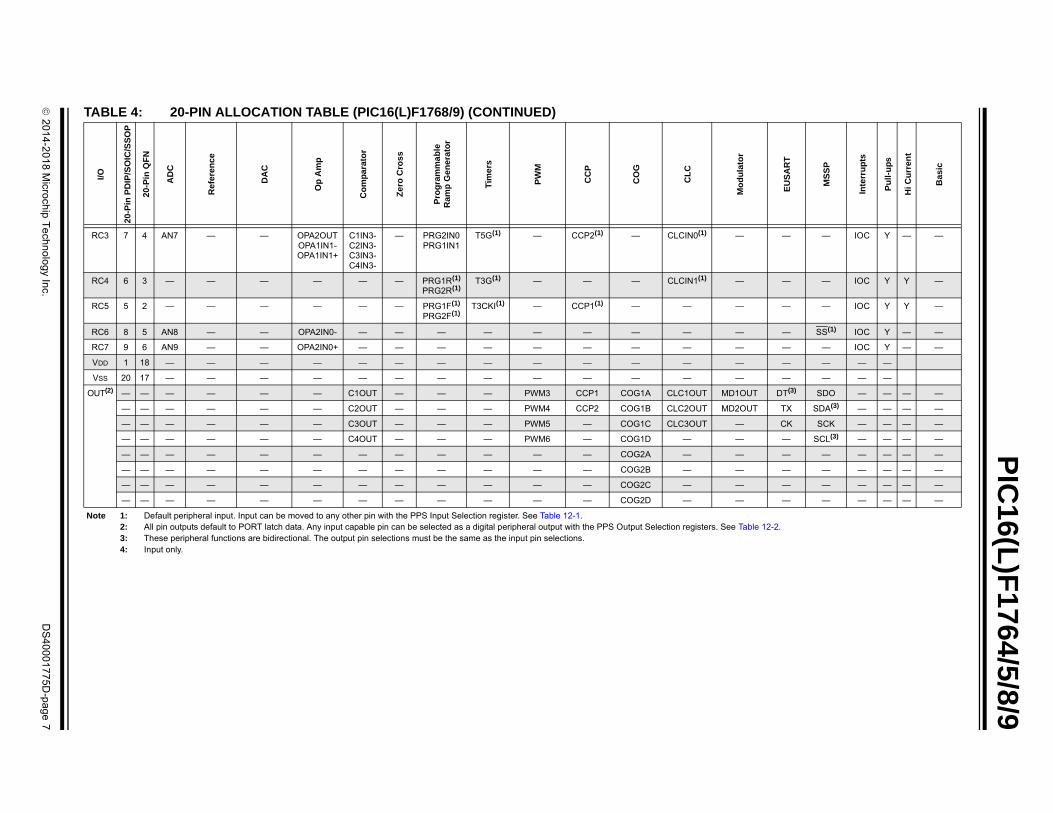
TABLE 4: 20-PIN ALLOCATION TABLE (PIC16(L)F1768/9)I/O
20-P
in P
DIP
/SO
IC/S
SO
P
20-P
in Q
FN
AD
C
Ref
eren
ce
DA
C
Op
Am
p
Co
mp
arat
or
Zer
o C
ross
Pro
gra
mm
ab
leR
amp
Gen
erat
or
Tim
ers
PW
M
CC
P
CO
G
CL
C
Mo
du
lato
r
EU
SA
RT
MS
SP
Inte
rru
pts
Pu
ll-u
ps
Hi C
urr
ent
Bas
ic
RA0 19 16 AN0 VREF-DAC1REF-DAC2REF-DAC3REF-DAC4REF-
DAC1OUT1DAC2OUT1DAC3OUT1DAC4OUT1
— C1IN0+C3IN0+
— — — — — — — — — — IOC Y — ICSPDAT
RA1 18 15 AN1 VREF+DAC1REF+DAC2REF+DAC3REF+DAC4REF+
— — C1IN0-C2IN0-C3IN0-C4IN0-
— — — — — — — — — — IOC Y — ICSPCLK
RA2 17 14 AN2 — — — — ZCD — T0CKI(1) — — COG1IN(1)
COG2IN(1)— — — — INT(1)
IOCY — —
RA3(4) 4 1 — — — — — — — T6IN(1) — — — — MD1CH(1)
MD2CH(1)— — IOC Y — VPP
MCLRICD
RA4 3 20 AN3 — — — — — — T1G(1)
SOSCO— — — — MD1CL(1)
MD2CL(1)— — IOC Y — OSC2
CLKOUT
RA5 2 19 — — — — — — — T1CKI(1)
T2IN(1)
SOSCI
— — — CLCIN3(1) MD1MOD(1)
MD2MOD(1)— — IOC Y — OSC1
CLKIN
RB4 13 10 AN10 — — OPA1IN0- — — — — — — — — — — SDI(1)
SDA(1,3)IOC Y — —
RB5 12 9 AN11 — — OPA1IN0+ — — — — — — — — — RX(1,3) — IOC Y — —
RB6 11 8 — — — — C1IN1+C3IN1+
— — — — — — — — — SCL(1)
SCK(1,3)IOC Y — —
RB7 10 7 — — — — C2IN1+C4IN1+
— — — — — — — — CK(1) — IOC Y — —
RC0 16 13 AN4 — — — C2IN0+C4IN0+
— — T5CKI(1) — — — — — — — IOC Y — —
RC1 15 12 AN5 — — — C1IN1-C2IN1-C3IN1-C4IN1-
— — T4IN(1) — — — CLCIN2(1) — — — IOC Y — —
RC2 14 11 AN6 — — OPA1OUTOPA2IN1-OPA2IN1+
C1IN2-C2IN2-
— PRG1IN0PRG2IN1
— — — — — — — — IOC Y — —
Note 1: Default peripheral input. Input can be moved to any other pin with the PPS Input Selection register. See Table 12-1.2: All pin outputs default to PORT latch data. Any input capable pin can be selected as a digital peripheral output with the PPS Output Selection registers. See Table 12-2.3: These peripheral functions are bidirectional. The output pin selections must be the same as the input pin selections.4: Input only.
2
01
4-2
01
8 M
icroch
ip T
ech
no
log
y Inc.
DS
40
00
17
75
D-p
ag
e 7
PIC
16(L)F
1764/5/8/9
RC3 7 4 AN7 — — OPA2OUTOPA1IN1-OPA1IN1+
C1IN3-C2IN3-C3IN3-C4IN3-
— PRG2IN0PRG1IN1
T5G(1) — CCP2(1) — CLCIN0(1) — — — IOC Y — —
RC4 6 3 — — — — — — PRG1R(1)
PRG2R(1)T3G(1) — — — CLCIN1(1) — — — IOC Y Y —
RC5 5 2 — — — — — — PRG1F(1)
PRG2F(1)T3CKI(1) — CCP1(1) — — — — — IOC Y Y —
RC6 8 5 AN8 — — OPA2IN0- — — — — — — — — — — SS(1) IOC Y — —
RC7 9 6 AN9 — — OPA2IN0+ — — — — — — — — — — — IOC Y — —
VDD 1 18 — — — — — — — — — — — — — — — — —
VSS 20 17 — — — — — — — — — — — — — — — — —
OUT(2) — — — — — — C1OUT — — — PWM3 CCP1 COG1A CLC1OUT MD1OUT DT(3) SDO — — — —
— — — — — — C2OUT — — — PWM4 CCP2 COG1B CLC2OUT MD2OUT TX SDA(3) — — — —
— — — — — — C3OUT — — — PWM5 — COG1C CLC3OUT — CK SCK — — — —
— — — — — — C4OUT — — — PWM6 — COG1D — — — SCL(3) — — — —
— — — — — — — — — — — — COG2A — — — — — — — —
— — — — — — — — — — — — COG2B — — — — — — — —
— — — — — — — — — — — — COG2C — — — — — — — —
— — — — — — — — — — — — COG2D — — — — — — — —
TABLE 4: 20-PIN ALLOCATION TABLE (PIC16(L)F1768/9) (CONTINUED)I/O
20-P
in P
DIP
/SO
IC/S
SO
P
20-P
in Q
FN
AD
C
Ref
eren
ce
DA
C
Op
Am
p
Co
mp
arat
or
Zer
o C
ross
Pro
gra
mm
ab
leR
amp
Gen
erat
or
Tim
ers
PW
M
CC
P
CO
G
CL
C
Mo
du
lato
r
EU
SA
RT
MS
SP
Inte
rru
pts
Pu
ll-u
ps
Hi C
urr
ent
Bas
ic
Note 1: Default peripheral input. Input can be moved to any other pin with the PPS Input Selection register. See Table 12-1.2: All pin outputs default to PORT latch data. Any input capable pin can be selected as a digital peripheral output with the PPS Output Selection registers. See Table 12-2.3: These peripheral functions are bidirectional. The output pin selections must be the same as the input pin selections.4: Input only.

2014-2018 Microchip Technology Inc. DS40001775D-page 8
PIC16(L)F1764/5/8/9
Table of Contents
1.0 Device Overview ........................................................................................................................................................................ 102.0 Enhanced Mid-Range CPU ........................................................................................................................................................ 223.0 Memory Organization ................................................................................................................................................................. 244.0 Device Configuration .................................................................................................................................................................. 625.0 Oscillator Module (with Fail-Safe Clock Monitor) ....................................................................................................................... 706.0 Resets ........................................................................................................................................................................................ 877.0 Interrupts .................................................................................................................................................................................... 968.0 Power-Down Mode (Sleep) ...................................................................................................................................................... 1099.0 Watchdog Timer (WDT) ........................................................................................................................................................... 11310.0 Flash Program Memory Control ............................................................................................................................................... 11711.0 I/O Ports ................................................................................................................................................................................... 13412.0 Peripheral Pin Select (PPS) Module ........................................................................................................................................ 15213.0 Interrupt-On-Change ................................................................................................................................................................ 16014.0 Fixed Voltage Reference (FVR) ............................................................................................................................................... 16715.0 Temperature Indicator Module ................................................................................................................................................. 17016.0 Analog-to-Digital Converter (ADC) Module .............................................................................................................................. 17217.0 5-Bit Digital-to-Analog Converter (DAC) Module...................................................................................................................... 18618.0 10-Bit Digital-to-Analog Converter (DAC) Module.................................................................................................................... 19019.0 Comparator Module.................................................................................................................................................................. 19620.0 Zero-Cross Detection (ZCD) Module........................................................................................................................................ 20621.0 Timer0 Module ......................................................................................................................................................................... 21222.0 Timer1/3/5 Module with Gate Control....................................................................................................................................... 21523.0 Timer2/4/6 Module ................................................................................................................................................................... 22624.0 Capture/Compare/PWM Modules ............................................................................................................................................ 24825.0 10-Bit Pulse-Width Modulation (PWM) Module ........................................................................................................................ 26126.0 16-Bit Pulse-Width Modulation (PWM) Module ........................................................................................................................ 26727.0 Complementary Output Generator (COG) Module................................................................................................................... 29328.0 Configurable Logic Cell (CLC).................................................................................................................................................. 33229.0 Operational Amplifier (OPA) Modules ...................................................................................................................................... 34630.0 Programmable Ramp Generator (PRG) Module ...................................................................................................................... 35231.0 Data Signal Modulator (DSM) .................................................................................................................................................. 36732.0 Master Synchronous Serial Port (MSSP) Module .................................................................................................................... 37733.0 Enhanced Universal Synchronous Asynchronous Receiver Transmitter (EUSART) ............................................................... 43234.0 In-Circuit Serial Programming™ (ICSP™) ............................................................................................................................... 46235.0 Instruction Set Summary .......................................................................................................................................................... 46436.0 Electrical Specifications............................................................................................................................................................ 47837.0 DC and AC Characteristics Graphs and Charts ....................................................................................................................... 51238.0 Development Support............................................................................................................................................................... 53439.0 Packaging Information.............................................................................................................................................................. 538Appendix A: Data Sheet Revision History ......................................................................................................................................... 559The Microchip Website ..................................................................................................................................................................... 560Customer Change Notification Service ............................................................................................................................................. 560Customer Support ............................................................................................................................................................................. 560Product Identification System ........................................................................................................................................................... 561

2014-2018 Microchip Technology Inc. DS40001775D-page 9
PIC16(L)F1764/5/8/9
TO OUR VALUED CUSTOMERS
It is our intention to provide our valued customers with the best documentation possible to ensure successful use of your Microchipproducts. To this end, we will continue to improve our publications to better suit your needs. Our publications will be refined andenhanced as new volumes and updates are introduced.
If you have any questions or comments regarding this publication, please contact the Marketing Communications Department viaE-mail at [email protected]. We welcome your feedback.
Most Current Data Sheet
To obtain the most up-to-date version of this data sheet, please register at our Worldwide Website at:
http://www.microchip.com
You can determine the version of a data sheet by examining its literature number found on the bottom outside corner of any page.The last character of the literature number is the version number, (e.g., DS30000000A is version A of document DS30000000).
Errata
An errata sheet, describing minor operational differences from the data sheet and recommended workarounds, may exist for currentdevices. As device/documentation issues become known to us, we will publish an errata sheet. The errata will specify the revisionof silicon and revision of document to which it applies.
To determine if an errata sheet exists for a particular device, please check with one of the following:
• Microchip’s Worldwide Website; http://www.microchip.com• Your local Microchip sales office (see last page)When contacting a sales office, please specify which device, revision of silicon and data sheet (include literature number) you areusing.
Customer Notification System
Register on our website at www.microchip.com to receive the most current information on all of our products.

2014-2018 Microchip Technology Inc. DS40001775D-page 10
PIC16(L)F1764/5/8/9
1.0 DEVICE OVERVIEW
The PIC16(L)F1764/5/8/9 are described within this datasheet. See Table 2 for available package configurations.
Figure 1-1 shows a block diagram of thePIC16(L)F1764/5 devices. Figure 1-2 shows a blockdiagram of the PIC16(L)F1768/9 devices. Table 1-2 andTable 1-3 show the pinout descriptions.
Refer to Table 1-1 for peripherals available per device.
TABLE 1-1: DEVICE PERIPHERAL SUMMARY
Peripheral
PIC
16(L
)F1
764
PIC
16(L
)F1
765
PIC
16(L
)F1
768
PIC
16(L
)F1
769
Analog-to-Digital Converter (ADC) ● ● ● ●
Fixed Voltage Reference (FVR) ● ● ● ●
Zero-Cross Detection (ZCD) ● ● ● ●
Temperature Indicator ● ● ● ●
Complementary Output Generator (COG)
COG1 ● ● ● ●
COG2 ● ●
Programmable Ramp Generator (PRG)
PRG1 ● ● ● ●
PRG2 ● ●
10-Bit Digital-to-Analog Converter (DAC)
DAC1 ● ● ● ●
DAC2 ● ●
5-Bit Digital-to-Analog Converter (DAC)
DAC3 ● ● ● ●
DAC4 ● ●
Capture/Compare/PWM (CCP/ECCP) Modules
CCP1 ● ● ● ●
CCP2 ● ●
Comparators
C1 ● ● ● ●
C2 ● ● ● ●
C3 ● ●
C4 ● ●
Configurable Logic Cell (CLC)
CLC1 ● ● ● ●
CLC2 ● ● ● ●
CLC3 ● ● ● ●
Data Signal Modulator (DSM)
DSM1 ● ● ● ●
DSM2 ● ●
Enhanced Universal Synchronous/Asynchronous Receiver/Transmitter (EUSART)
EUSART ● ● ● ●
Master Synchronous Serial Ports
MSSP ● ● ● ●
Op Amp
Op Amp 1 ● ● ● ●
Op Amp 2 ● ●
10-Bit Pulse-Width Modulator (PWM)
PWM3 ● ● ● ●
PWM4 ● ●
16-Bit Pulse-Width Modulator (PWM)
PWM5 ● ● ● ●
PWM6 ● ●
8-Bit Timers
Timer0 ● ● ● ●
Timer2 ● ● ● ●
Timer4 ● ● ● ●
Timer6 ● ● ● ●
16-Bit Timers
Timer1 ● ● ● ●
Timer3 ● ● ● ●
Timer5 ● ● ● ●
TABLE 1-1: DEVICE PERIPHERAL SUMMARY (CONTINUED)
Peripheral
PIC
16
(L)F
176
4
PIC
16
(L)F
176
5
PIC
16
(L)F
176
8
PIC
16
(L)F
176
9

2014-2018 Microchip Technology Inc. DS40001775D-page 11
PIC16(L)F1764/5/8/9
1.1 Register and Bit Naming Conventions
1.1.1 REGISTER NAMES
When there are multiple instances of the sameperipheral in a device, the peripheral control registerswill be depicted as the concatenation of a peripheralidentifier, peripheral instance and control identifier. Thecontrol registers section will show just one instance ofall the register names with an ‘x’ in the place of theperipheral instance number. This naming conventionmay also be applied to peripherals when there is onlyone instance of that peripheral in the device to maintaincompatibility with other devices in the family thatcontain more than one.
1.1.2 BIT NAMES
There are two variants for bit names:
• Short name: Bit function abbreviation
• Long name: Peripheral abbreviation + short name
1.1.2.1 Short Bit Names
Short bit names are an abbreviation for the bit function.For example, some peripherals are enabled with theEN bit. The bit names shown in the registers are theshort name variant.
Short bit names are useful when accessing bits in Cprograms. The general format for accessing bits by theshort name is RegisterNamebits.ShortName. Forexample, the enable bit, EN, in the COG1CON0 regis-ter can be set in C programs with the instructionCOG1CON0bits.EN = 1.
Short names are generally not useful in assemblyprograms because the same name may be used bydifferent peripherals in different bit positions. When thisoccurs, during the include file generation, all instancesof that short bit name are appended with an underscoreplus the name of the register in which the bit resides toavoid naming contentions.
1.1.2.2 Long Bit Names
Long bit names are constructed by adding a peripheralabbreviation prefix to the short name. The prefix isunique to the peripheral thereby making every long bitname unique. The long bit name for the COG1 enablebit is the COG1 prefix, G1, appended with the enablebit short name, EN, resulting in the unique bit nameG1EN.
Long bit names are useful in both C and assembly pro-grams. For example, in C the COG1CON0 enable bitcan be set with the G1EN = 1 instruction. In assembly,this bit can be set with the BSF COG1CON0,G1ENinstruction.
1.1.2.3 Bit Fields
Bit fields are two or more adjacent bits in the sameregister. Bit fields adhere only to the short bit namingconvention. For example, the three Least Significantbits of the COG1CON0 register contain the modecontrol bits. The short name for this field is MD. Thereis no long bit name variant. Bit field access is onlypossible in C programs. The following exampledemonstrates a C program instruction for setting theCOG1 to the Push-Pull mode:
COG1CON0bits.MD = 0x5;
Individual bits in a bit field can also be accessed withlong and short bit names. Each bit is the field nameappended with the number of the bit position within thefield. For example, the Most Significant mode bit hasthe short bit name MD2, and the long bit name isG1MD2. The following two examples demonstrateassembly program sequences for setting the COG1 toPush-Pull mode:
Example 1:
MOVLW ~(1<<G1MD1)ANDWF COG1CON0,FMOVLW 1<<G1MD2 | 1<<G1MD0IORWF COG1CON0,F
Example 2:
BSF COG1CON0,G1MD2BCF COG1CON0,G1MD1BSF COG1CON0,G1MD0
1.1.3 REGISTER AND BIT NAMING EXCEPTIONS
1.1.3.1 Status, Interrupt and Mirror Bits
Status, interrupt enables, interrupt flags and mirror bitsare contained in registers that span more than oneperipheral. In these cases, the bit name shown isunique, so there is no prefix or short name variant.
1.1.3.2 Legacy Peripherals
There are some peripherals that do not strictly adhereto these naming conventions. Peripherals that haveexisted for many years and are present in almost everydevice are the exceptions. These exceptions werenecessary to limit the adverse impact of the newconventions on legacy code. Peripherals that doadhere to the new convention will include a table in theregisters section indicating the long name prefix foreach peripheral instance. Peripherals that fall into theexception category will not have this table. Theseperipherals include, but are not limited to, the following:
• EUSART
• MSSP

2014-2018 Microchip Technology Inc. DS40001775D-page 12
PIC16(L)F1764/5/8/9
FIGURE 1-1: PIC16(L)F1764/5 BLOCK DIAGRAM
PORTA
PORTC
Note 1: See applicable chapters for more information on peripherals.
CPU
ProgramFlash Memory
RAM
TimingGeneration
LFINTOSCOscillator
MCLR
Figure 1-1
CLKIN
CLKOUT
ADC10-Bit
FVRTemp.
Indicator EUSART
ComparatorsMSSPTimersTimers
DACCCP
PWMsOp Amp
HFINTOSC/
CLCs
COG
ZCD
DSM
PRG
8-Bit 16-BitDAC5-Bit
10-Bit

2014-2018 Microchip Technology Inc. DS40001775D-page 13
PIC16(L)F1764/5/8/9
FIGURE 1-2: PIC16(L)F1768/9 BLOCK DIAGRAM
PORTA
PORTB
PORTCCPU
ProgramFlash Memory
RAM
TimingGeneration
LFINTOSCOscillator
MCLR
Figure 1-1
CLKIN
CLKOUT
ADC10-Bit
FVRTemp.
Indicator EUSART
ComparatorsMSSPTimersTimers
DACsCCPs
PWMsOp Amps
HFINTOSC/
CLCs
COG
ZCD
DSMs
PRGs
8-Bit 16-BitDACs5-Bit
10-Bit
Note 1: See applicable chapters for more information on peripherals.

2014-2018 Microchip Technology Inc. DS40001775D-page 14
PIC16(L)F1764/5/8/9
TABLE 1-2: PIC16(L)F1764/5 PINOUT DESCRIPTION
Name FunctionInput Type
Output Type
Description
RA0/AN0/C1IN0+/VREF-/DAC1REF-/DAC3REF-/DAC1OUT1/DAC3OUT1/ICSPDAT
RA0 TTL/ST CMOS General purpose I/O.
AN0 AN — ADC Channel 0 input.
C1IN0+ AN — Comparator C1 positive input.
VREF- AN — ADC negative reference.
DAC1REF- AN — DAC1 negative reference.
DAC3REF- AN — DAC3 negative reference.
DAC1OUT1 — AN DAC1 voltage output.
DAC3OUT1 — AN DAC3 voltage output.
ICSPDAT ST CMOS ICSP™ data I/O.
RA1/AN1/C1IN0-/C2IN0-/VREF+/DAC1REF+/DAC3REF+/ICSPCLK
RA1 TTL/ST CMOS General purpose I/O.
AN1 AN — ADC Channel 1 input.
C1IN0- AN — Comparator C1 negative input.
C2IN0- AN — Comparator C2 negative input.
VREF+ AN — ADC positive reference.
DAC1REF+ AN — DAC1 positive reference.
DAC3REF+ AN — DAC3 positive reference.
ICSPCLK ST — Serial programming clock.
RA2/AN2/ZCD/T0CKI/COG1IN/INT
RA2 TTL/ST CMOS General purpose I/O.
AN2 AN — ADC Channel 2 input.
ZCD AN — Zero-Cross Detection input.
T0CKI TTL/ST — Timer0 clock input.
COG1IN(1) TTL/ST — Complementary Output Generator 1 input.
INT(1) TTL/ST — Interrupt input.
RA3/T6IN/MD1CH/MCLR/VPP RA3 TTL/ST — General purpose input.
T6IN(1) TTL/ST — Timer6 clock input.
MD1CH(1) TTL/ST — Data Signal Modulator 1 high carrier input.
MCLR ST — Master Clear input.
VPP HV — Programming enable.
RA4/AN3/SOSCO/T1G/MD1CL/OSC2/CLKOUT
RA4 TTL/ST CMOS General purpose I/O.
AN3 AN — ADC Channel 3 input.
SOSCO — XTAL Secondary Oscillator connection.
T1G(1) TTL/ST — Timer1 gate input.
MD1CL(1) TTL/ST — Data Signal Modulator 1 low carrier input.
OSC2 — XTAL Crystal/Resonator (LP, XT, HS modes).
CLKOUT — CMOS FOSC/4 output.
Legend: AN = Analog input or output CMOS = CMOS compatible input or output OD = Open-DrainTTL = TTL compatible input ST = Schmitt Trigger input with CMOS levels I2C = Schmitt Trigger input with I2C HV = High Voltage XTAL = Crystal levels
Note 1: Default peripheral input. Alternate pins can be selected as the peripheral input with the PPS Input Selection registers.2: All pin digital outputs default to PORT latch data. Alternate outputs can be selected as peripheral digital outputs with the
PPS Output Selection registers.3: These peripheral functions are bidirectional. The output pin selections must be the same as the input pin selections.

2014-2018 Microchip Technology Inc. DS40001775D-page 15
PIC16(L)F1764/5/8/9
RA5/T1CKI/T2IN/CLCIN3/MD1MOD/SOSCI/OSC1/CLKIN
RA5 TTL/ST CMOS General purpose I/O.
T1CKI(1) TTL/ST — Timer1 clock input.
T2IN(1) TTL/ST — Timer2 clock input.
CLCIN3(1) TTL/ST — CLC Input 3.
MD1MOD(1) TTL/ST — Data Signal Modulator modulation input.
SOSCI — XTAL Secondary Oscillator connection.
OSC1 XTAL — Crystal/Resonator (LP, XT, HS modes).
CLKIN ST — External Clock input (EC mode).
RC0/AN4/OPA1IN+/C2IN0+/T5CKI/SCL/SCK
RC0 TTL/ST CMOS General purpose I/O.
AN4 AN ADC Channel 4 input.
OPA1IN+ AN — Operational Amplifier 1 non-inverting input.
C2IN0+ AN — Comparator 2 positive input.
T5CKI(1) TTL/ST — Timer5 clock input.
SCL(1,3) I2C — I2C clock output.
SCK(1) TTL/ST — SPI clock input.
RC1/AN5/OPA1IN-/C1IN1-/C2IN1-/T4IN/CLCIN2/SDI/SDA
RC1 TTL/ST CMOS General purpose I/O.
AN5 AN XTAL ADC Channel 5 input.
OPA1IN- AN — Operational Amplifier 1 inverting input.
C1IN1- AN — Comparator 1 negative input.
C2IN1- AN — Comparator 2 negative input.
T4IN(1) TTL/ST — Timer4 clock input.
CLCIN2(1) TTL/ST — CLC Input 2.
SDI(1) TTL/ST — SPI data input.
SDA(1) I2C — I2C data output.
RC2/AN6/OPA1OUT/C1IN2-/C2IN2-/PRG1IN0
RC2 TTL/ST CMOS General purpose I/O.
AN6 AN — ADC Channel 6 input.
OPA1OUT — AN Operational Amplifier 1 output.
C1IN2- AN — Comparator 1 negative input.
C2IN2- AN — Comparator 2 negative input.
PRG1IN0 AN — Ramp Generator 1 reference voltage input.
RC3/AN7/C1IN3-/C2IN3-/T5G/CLCIN0/SS
RC3 TTL/ST CMOS General purpose I/O.
AN7 AN — ADC Channel 7 input.
C1IN3- AN — Comparator 1 negative input.
C2IN3- AN — Comparator 2 negative input.
T5G(1) TTL/ST — Timer5 gate input.
CLCIN0(1) TTL/ST — CLC Input 0.
SS(1) TTL/ST — SPI Slave Select input.
TABLE 1-2: PIC16(L)F1764/5 PINOUT DESCRIPTION (CONTINUED)
Name FunctionInput Type
Output Type
Description
Legend: AN = Analog input or output CMOS = CMOS compatible input or output OD = Open-DrainTTL = TTL compatible input ST = Schmitt Trigger input with CMOS levels I2C = Schmitt Trigger input with I2C HV = High Voltage XTAL = Crystal levels
Note 1: Default peripheral input. Alternate pins can be selected as the peripheral input with the PPS Input Selection registers.2: All pin digital outputs default to PORT latch data. Alternate outputs can be selected as peripheral digital outputs with the
PPS Output Selection registers.3: These peripheral functions are bidirectional. The output pin selections must be the same as the input pin selections.

2014-2018 Microchip Technology Inc. DS40001775D-page 16
PIC16(L)F1764/5/8/9
RC4/T3G/PRG1R/CLCIN1/CK RC4 TTL/ST CMOS General purpose I/O.
T3G(1) TTL/ST — Timer3 gate input.
PRG1R(1) TTL/ST — Ramp generator set_rising input.
CLCIN1(1) TTL/ST — CLC Input 1.
CK(1) TTL/ST — EUSART clock input.
RC5/T3CKI/PRG1F/CCP1/RX RC5 TTL/ST CMOS General purpose I/O.
T3CKI(1) TTL/ST — Timer3 clock input.
PRG1F(1) TTL/ST — Ramp generator set_falling input.
CCP1(1) TTL/ST — CCP1 capture input.
RX(1,3) TTL/ST — EUSART receive input.
VDD VDD Power — Positive supply.
VSS VSS Power — Ground reference.
OUT(2) C1OUT CMOS Comparator 1 output.
C2OUT CMOS Comparator 2 output.
CCP1 CMOS Compare/PWM1 output.
MD1OUT CMOS Data Signal Modulator 1 output.
PWM3 CMOS PWM3 output.
PWM5 CMOS PWM5 output.
COG1A CMOS Complementary Output Generator Output A.
COG1B CMOS Complementary Output Generator Output B.
COG1C CMOS Complementary Output Generator Output C.
COG1D CMOS Complementary Output Generator Output D.
SDA(3) OD I2C data output.
SCK CMOS SPI clock output.
SCL(3) OD I2C clock output.
SDO CMOS SPI data output.
TX CMOS EUSART asynchronous TX data out.
CK CMOS EUSART synchronous clock out.
DT(3) CMOS EUSART synchronous data output.
CLC1OUT CMOS Configurable Logic Cell 1 output.
CLC2OUT CMOS Configurable Logic Cell 2 output.
CLC3OUT CMOS Configurable Logic Cell 3 output.
TABLE 1-2: PIC16(L)F1764/5 PINOUT DESCRIPTION (CONTINUED)
Name FunctionInput Type
Output Type
Description
Legend: AN = Analog input or output CMOS = CMOS compatible input or output OD = Open-DrainTTL = TTL compatible input ST = Schmitt Trigger input with CMOS levels I2C = Schmitt Trigger input with I2C HV = High Voltage XTAL = Crystal levels
Note 1: Default peripheral input. Alternate pins can be selected as the peripheral input with the PPS Input Selection registers.2: All pin digital outputs default to PORT latch data. Alternate outputs can be selected as peripheral digital outputs with the
PPS Output Selection registers.3: These peripheral functions are bidirectional. The output pin selections must be the same as the input pin selections.

2014-2018 Microchip Technology Inc. DS40001775D-page 17
PIC16(L)F1764/5/8/9
TABLE 1-3: PIC16(L)F1768/9 PINOUT DESCRIPTION
Name FunctionInput Type
Output Type
Description
RA0/AN0/C1IN0+/C3IN0+/VREF-/DAC1REF-/DAC2REF-/DAC3REF-/DAC4REF-/DAC1OUT1/DAC2OUT1./DAC3OUT1/DAC4OUT1/ICSPDAT
RA0 TTL/ST CMOS General purpose I/O.
AN0 AN — ADC Channel 0 input.
C1IN0+ AN — Comparator C1 positive input.
C3IN0+ AN Comparator C3 positive input.
DAC1REF- AN — DAC1 negative reference.
DAC2REF- AN — DAC2 negative reference.
DAC3REF- AN — DAC3 negative reference.
DAC4REF- AN — DAC4 negative reference.
DAC1OUT1 — AN DAC1 voltage output.
DAC2OUT1 — AN DAC2 voltage output.
DAC3OUT1 — AN DAC3 voltage output.
DAC4OUT1 — AN DAC4 voltage output.
VREF- AN — ADC negative reference.
ICSPDAT ST CMOS ICSP™ data I/O.
RA1/AN1/C1IN0-/C2IN0-/C3IN0-/C4IN0-/VREF+/DAC1REF+/DAC2REF+/DAC3REF+/DAC4REF+/ICSPCLK
RA1 TTL/ST CMOS General purpose I/O.
AN1 AN — ADC Channel 1 input.
C1IN0- AN — Comparator C1 negative input.
C2IN0- AN — Comparator C2 negative input.
C3IN0- AN — Comparator C3 negative input.
C4IN0- AN — Comparator C4 negative input.
DAC1REF+ AN — DAC1 positive reference.
DAC2REF+ AN — DAC2 positive reference.
DAC3REF+ AN — DAC3 positive reference.
DAC4REF+ AN — DAC4 positive reference.
VREF+ AN — ADC positive reference.
ICSPCLK ST — Serial programming clock.
RA2/AN2/ZCD/T0CKI/COG1IN/COG2IN/INT
RA2 TTL/ST CMOS General purpose I/O.
AN2 AN — ADC Channel 2 input.
ZCD AN — Zero-Cross Detection input.
T0CKI(1) TTL/ST — Timer0 clock input.
COG1IN(1) TTL/ST — Complementary Output Generator 1 input.
COG2IN(1) TTL/ST — Complementary Output Generator 2 input.
INT(1) TTL/ST — Interrupt input.
RA3/T6IN/MD1CH/MD2CH/MCLR/VPP
RA3 TTL/ST — General purpose input.
T6IN(1) TTL/ST — Timer6 clock input.
MD1CH(1) TTL/ST — Data Signal Modulator 1 high carrier input.
MD2CH(1) TTL/ST — Data Signal Modulator 2 high carrier input.
MCLR ST — Master Clear input.
VPP HV — Programming enable.
Legend: AN = Analog input or output CMOS = CMOS compatible input or output OD = Open-DrainTTL = TTL compatible input ST = Schmitt Trigger input with CMOS levels I2C = Schmitt Trigger input with I2C HV = High Voltage XTAL = Crystal levels
Note 1: Default peripheral input. Alternate pins can be selected as the peripheral input with the PPS Input Selection registers.2: All pin digital outputs default to PORT latch data. Alternate outputs can be selected as peripheral digital outputs with the
PPS Output Selection registers.3: These peripheral functions are bidirectional. The output pin selections must be the same as the input pin selections.

2014-2018 Microchip Technology Inc. DS40001775D-page 18
PIC16(L)F1764/5/8/9
RA4/AN3/SOSCO/T1G/DSM1CL/DSM2CL/OSC2/CLKOUT
RA4 TTL/ST CMOS General purpose I/O.
AN3 AN — ADC Channel 3 input.
SOSCO — XTAL Secondary Oscillator connection.
T1G(1) TTL/ST — Timer1 gate input.
DSM1CL(1) TTL/ST — Data Signal Modulator 1 low carrier input.
DSM2CL(1) TTL/ST — Data Signal Modulator 2 low carrier input.
OSC2 — XTAL Crystal/Resonator (LP, XT, HS modes).
CLKOUT — CMOS FOSC/4 output.
RA5/T1CKI/T2IN/CLCIN3/DSM1MOD/DSM2MOD/SOSCI/OSC1/CLKIN
RA5 TTL/ST CMOS General purpose I/O.
T1CKI(1) TTL/ST — Timer1 clock input.
T2IN(1) TTL/ST — Timer2 clock input.
CLCIN3(1) TTL/ST — CLC Input 3.
DSM1MOD(1) TTL/ST — Data Signal Modulator 1 modulation input.
DSM2MOD(1) TTL/ST — Data Signal Modulator 2 modulation input.
SOSCI XTAL — Secondary Oscillator connection.
OSC1 XTAL — Crystal/Resonator (LP, XT, HS modes).
CLKIN ST — External Clock input (EC mode).
RB4/AN10/OPA1IN0-/SDI/SDA RB4 TTL/ST CMOS General purpose I/O.
AN10 AN — ADC Channel 10 input.
OPA1IN0- AN — Operational Amplifier 1 inverting input.
SDI(1) TTL/ST — SPI data input.
SDA(1,3) I2C — I2C data output.
RB5/AN11/OPA1IN0+/RX RB5 TTL/ST CMOS General purpose I/O.
AN11 AN — ADC Channel 11 input.
OPA1IN0+ AN — Operational Amplifier 1 non-inverting input.
RX(1,3) TTL/ST — EUSART receive input.
RB6/C1IN1+/C3IN1+/SCK/SCL RB6 TTL/ST CMOS General purpose I/O.
C1IN1+ AN — Comparator C1 positive input.
C3IN1+ AN — Comparator C3 positive input.
SCK(1) TTL/ST — SPI clock input.
SCL(1,3) I2C — I2C clock output.
RB7/C2IN1+/C4IN1+/CK RB7 TTL/ST CMOS General purpose I/O.
C2IN1+ AN — Comparator C2 positive input.
C4IN1+ AN — Comparator C4 positive input.
CK(1) TTL/ST — EUSART clock input.
RC0/AN4/C2IN0+/C4IN0+/T5CKI
RC0 TTL/ST CMOS General purpose I/O.
AN4 AN ADC Channel 4 input.
C2IN0+ AN — Comparator C2 positive input.
C4IN0+ AN — Comparator C4 positive input.
T5CKI(1) TTL/ST — Timer5 clock input.
TABLE 1-3: PIC16(L)F1768/9 PINOUT DESCRIPTION (CONTINUED)
Name FunctionInput Type
Output Type
Description
Legend: AN = Analog input or output CMOS = CMOS compatible input or output OD = Open-DrainTTL = TTL compatible input ST = Schmitt Trigger input with CMOS levels I2C = Schmitt Trigger input with I2C HV = High Voltage XTAL = Crystal levels
Note 1: Default peripheral input. Alternate pins can be selected as the peripheral input with the PPS Input Selection registers.2: All pin digital outputs default to PORT latch data. Alternate outputs can be selected as peripheral digital outputs with the
PPS Output Selection registers.3: These peripheral functions are bidirectional. The output pin selections must be the same as the input pin selections.

2014-2018 Microchip Technology Inc. DS40001775D-page 19
PIC16(L)F1764/5/8/9
RC1/AN5/C1IN1-/C2IN1-/C3IN1-/C4IN1-/T4IN/CLCIN2
RC1 TTL/ST CMOS General purpose I/O.
AN5 AN XTAL ADC Channel 5 input.
C1IN1- AN — Comparator 1 negative input.
C2IN1- AN — Comparator 2 negative input.
C3IN1- AN — Comparator 3 negative input.
C4IN1- AN — Comparator 4 negative input.
T4IN(1) TTL/ST — Timer4 clock input.
CLCIN2(1) TTL/ST — CLC Input 2.
RC2/AN6/OPA1OUT/OPA2IN1-/OPA2IN1+/C1IN2-/C2IN2-/PRG1IN0/PRG2IN1
RC2 TTL/ST CMOS General purpose I/O.
AN6 AN — ADC Channel 6 input.
OPA1OUT — AN Operational Amplifier 1 output.
OPA2IN1- AN Operational Amplifier 2 inverting input.
OPA2IN1+ AN Operational Amplifier 2 non-inverting input.
C1IN2- AN — Comparator 1 negative input.
C2IN2- AN — Comparator 2 negative input.
PRG1IN0 AN — Ramp Generator 1 reference voltage input.
PRG2IN1 AN — Ramp Generator 2 reference voltage input.
RC3/AN7/OPA2OUT/OPA1IN1-/OPA1IN1+/C1IN3-/C2IN3-/C3IN3-/C4IN3-/PRG1IN1/PRG2IN0/T5G/CCP2/CLCIN0
RC3 TTL/ST CMOS General purpose I/O.
AN7 AN — ADC Channel 7 input.
OPA2OUT — AN Operational Amplifier 2 output.
OPA1IN1- AN Operational Amplifier 1 inverting input.
OPA1IN1+ AN Operational Amplifier 1 non-inverting input.
C1IN3- AN — Comparator 1 negative input.
C2IN3- AN — Comparator 2 negative input.
C3IN3- AN — Comparator 3 negative input.
C4IN3- AN — Comparator 4 negative input.
PRG1IN1 AN — Ramp Generator 1 reference voltage input.
PRG2IN0 AN — Ramp Generator 2 reference voltage input.
T5G(1) TTL/ST — Timer5 gate input.
CCP2(1) TTL/ST — CCP2 capture input.
CLCIN0(1) TTL/ST — CLC Input 0.
RC4/T3G/PRG1R/PRG2R/CLCIN1
RC4 TTL/ST CMOS General purpose I/O.
T3G(1) TTL/ST — Timer3 gate input.
PRG1R(1) TTL/ST — Ramp Generator 1 set_rising input.
PRG2R(1) TTL/ST — Ramp Generator 2 set_rising input.
CLCIN1(1) TTL/ST — CLC Input 1.
RC5/T3CKI/PRG1F/PRG2F/CCP1
RC5 TTL/ST CMOS General purpose I/O.
T3CKI(1) TTL/ST — Timer3 clock input.
PRG1F(1) TTL/ST — Ramp Generator 1 set_falling input.
PRG2F(1) TTL/ST — Ramp Generator 2 set_falling input.
CCP1(1) TTL/ST — CCP1 capture input.
TABLE 1-3: PIC16(L)F1768/9 PINOUT DESCRIPTION (CONTINUED)
Name FunctionInput Type
Output Type
Description
Legend: AN = Analog input or output CMOS = CMOS compatible input or output OD = Open-DrainTTL = TTL compatible input ST = Schmitt Trigger input with CMOS levels I2C = Schmitt Trigger input with I2C HV = High Voltage XTAL = Crystal levels
Note 1: Default peripheral input. Alternate pins can be selected as the peripheral input with the PPS Input Selection registers.2: All pin digital outputs default to PORT latch data. Alternate outputs can be selected as peripheral digital outputs with the
PPS Output Selection registers.3: These peripheral functions are bidirectional. The output pin selections must be the same as the input pin selections.

2014-2018 Microchip Technology Inc. DS40001775D-page 20
PIC16(L)F1764/5/8/9
RC6/AN8/OPA2IN0-/SS RC6 TTL/ST CMOS General purpose I/O.
AN8 AN — ADC Channel 8 input.
OPA2IN0- AN — Operational Amplifier 2 inverting input.
SS(1) TTL/ST — SPI Slave Select input.
RC7/AN9/OPA2IN0+ RC7 TTL/ST CMOS General purpose I/O.
AN9 AN — ADC Channel 9 input.
OPA2IN0+ AN — Operational Amplifier 2 non-inverting input.
VDD VDD Power — Positive supply.
VSS VSS Power — Ground reference.
OUT(2) C1OUT CMOS Comparator 1 output.
C2OUT CMOS Comparator 2 output.
C3OUT CMOS Comparator 3 output.
C4OUT CMOS Comparator 4 output.
CCP1 CMOS Compare/PWM1 output.
CCP2 CMOS Compare/PWM2 output.
MD1OUT CMOS Data Signal Modulator 1 output.
MD2OUT CMOS Data Signal Modulator 2 output.
PWM3 CMOS PWM3 output.
PWM4 CMOS PWM4 output.
PWM5 CMOS PWM5 output.
PWM6 CMOS PWM6 output.
COG1A CMOS Complementary Output Generator 1 Output A.
COG1B CMOS Complementary Output Generator 1 Output B.
COG1C CMOS Complementary Output Generator 1 Output C.
COG1D CMOS Complementary Output Generator 1 Output D.
COG2A CMOS Complementary Output Generator 2 Output A.
COG2B CMOS Complementary Output Generator 2 Output B.
COG2C CMOS Complementary Output Generator 2 Output C.
COG2D CMOS Complementary Output Generator 2 Output D.
SDA(3) OD I2C data output.
SCK CMOS SPI clock output.
SCL(3) OD I2C clock output.
SDO CMOS SPI data output.
TX CMOS EUSART asynchronous TX data out.
CK CMOS EUSART synchronous clock out.
DT(3) CMOS EUSART synchronous data output.
CLC1OUT CMOS Configurable Logic Cell 1 output.
CLC2OUT CMOS Configurable Logic Cell 2 output.
CLC3OUT CMOS Configurable Logic Cell 3 output.
TABLE 1-3: PIC16(L)F1768/9 PINOUT DESCRIPTION (CONTINUED)
Name FunctionInput Type
Output Type
Description
Legend: AN = Analog input or output CMOS = CMOS compatible input or output OD = Open-DrainTTL = TTL compatible input ST = Schmitt Trigger input with CMOS levels I2C = Schmitt Trigger input with I2C HV = High Voltage XTAL = Crystal levels
Note 1: Default peripheral input. Alternate pins can be selected as the peripheral input with the PPS Input Selection registers.2: All pin digital outputs default to PORT latch data. Alternate outputs can be selected as peripheral digital outputs with the
PPS Output Selection registers.3: These peripheral functions are bidirectional. The output pin selections must be the same as the input pin selections.

2014-2018 Microchip Technology Inc. DS40001775D-page 21
PIC16(L)F1764/5/8/9
1.2 Peripheral Connection Matrix
Input selection multiplexers on many of the peripheralsenable selecting the output of another peripheral, suchthat the signal path is contained entirely within thedevice. Although the peripheral output can also be
routed to a pin with the PPS selection feature, it is notnecessary to do so. Table 1-4 shows all the possibleinter-peripheral signal connections. Please refer to thecorresponding peripheral section to obtain themultiplexer selection codes for the desired connection.
TABLE 1-4: PERIPHERAL CONNECTION MATRIX
Peripheral Input
Peripheral Output
AD
C T
rig
ger
CO
G C
lock
CO
G R
isin
g/F
allin
g
CO
G S
hu
tdo
wn
10-B
it D
AC
5-B
it D
AC
PR
G A
nal
og
Inp
ut
PR
G R
isin
g/F
allin
g
Co
mp
arat
or
+
Co
mp
arat
or
-
CL
C
DS
M C
H
DS
M C
L
DS
M M
od
Op
Am
p +
Op
Am
p -
Op
Am
p O
verr
ide
10-B
it P
WM
16-B
it P
WM
CC
P C
aptu
re
CC
P C
lock
Tim
er2/
4/6
Clo
ck
Tim
er2/
4/6
Res
et
Tim
er1/
3/5
Gat
e
Tim
er0
Clo
ck
FVR ● ● ● ● ● ● ●
ZCD ● ● ●
PRG ● ● ●
10-Bit DAC ● ● ● ●
5-Bit DAC ● ● ● ●
CCP ● ● ● ● ● ● ● ● ●
Comparator (sync) ● ● ● ● ● ● ●
Comparator (async) ● ● ●
CLC ● ● ● ● ● ● ● ● ● ● ●
DSM
COG ●
EUSART TX/CK ● ●
EUSART DT ● ●
MSSP SCK/SCL ● ●
MSSP SDO/SDA ● ●
Op Amp ●
10-Bit PWM ● ● ● ● ● ● ● ● ●
16-Bit PWM ● ● ● ● ● ● ● ● ●
Timer0 Overflow ● ● ●
Timer2 = T2PR ● ● ● ● ●
Timer4 = T4PR ● ● ● ● ●
Timer6 = T6PR ● ● ● ● ●
Timer2 Postscale ● ● ● ● ● ●
Timer4 Postscale ● ● ● ● ● ●
Timer6 Postscale ● ● ● ● ● ●
Timer1 Overflow ● ● ● ●
Timer3 Overflow ● ● ● ●
Timer5 Overflow ● ● ● ●
SOSC ● ●
FOSC/4 ● ●
FOSC ● ● ● ● ● ●
HFINTOSC ● ● ● ● ● ●
LFINTOSC ● ● ●
MFINTOSC ●
IOCIF ● ● ●
PPS Input Pin ● ● ● ● ● ● ● ● ● ● ● ●

2014-2018 Microchip Technology Inc. DS40001775D-page 22
PIC16(L)F1764/5/8/9
2.0 ENHANCED MID-RANGE CPU
This family of devices contains an enhanced mid-range8-bit CPU core. The CPU has 49 instructions. Interruptcapability includes automatic context saving. Thehardware stack is 16 levels deep and has Overflow andUnderflow Reset capability. Direct, Indirect and
Relative Addressing modes are available. Two FileSelect Registers (FSRs) provide the ability to readprogram and data memory.
• Automatic Interrupt Context Saving
• 16-Level Stack with Overflow and Underflow
• File Select Registers
• Instruction Set
FIGURE 2-1: CORE BLOCK DIAGRAM
8
14ProgramBus
Instruction reg
Program Counter
16-Level Stack(15-bit)
Direct Addr 7
12
Addr MUX
FSR reg
MUX
ALU
Power-upTimer
OscillatorStart-up Timer
Power-onReset
WatchdogTimer
InstructionDecode and
Control
TimingGeneration
OSC1/CLKIN
OSC2/CLKOUT
8
8
Brown-outReset
12
3
InternalOscillator
Block
8
Instruction reg7
Addr MUX
FSR reg
MUX
ALU
W Reg
8
3
InternalOscillator
Block
15 Data Bus 8
Instruction Reg7
RAM Addr
Addr MUX
IndirectAddr
FSR0 Reg
STATUS Reg
MUX
ALU
VDD
8
3
VSS
InternalOscillator
Block
RAM
FSR1 Reg
15
15
MU
X
15
Program MemoryRead (PMR)
12
FSR regFSR regBSR Reg
5
ConfigurationConfigurationConfiguration
Flash
Program
Memory
2014-2018 Microchip Technology Inc. DS40001775D-page 23
PIC16(L)F1764/5/8/9
2.1 Automatic Interrupt Context Saving
During interrupts, certain registers are automaticallysaved in shadow registers and restored when returningfrom the interrupt. This saves stack space and usercode. See Section 7.5 “Automatic Context Saving”for more information.
2.2 16-Level Stack with Overflow and Underflow
These devices have a hardware stack memory 15 bitswide and 16 words deep. A Stack Overflow or Under-flow will set the appropriate bit (STKOVF or STKUNF)in the PCON register, and if enabled, will cause aSoftware Reset. See Section 3.5 “Stack” for moredetails.
2.3 File Select Registers
There are two 16-bit File Select Registers (FSRs).FSRs can access all file registers and programmemory, which allows one Data Pointer for all memory.When an FSRn points to program memory, there is oneadditional instruction cycle in instructions using INDFn toallow the data to be fetched. General purpose memorycan now also be addressed linearly, providing the abilityto access contiguous data larger than 80 bytes. Thereare also new instructions to support the FSRs. SeeSection 3.6 “Indirect Addressing” for more details.
2.4 Instruction Set
There are 49 instructions for the enhanced mid-rangeCPU to support the features of the CPU. SeeSection 35.0 “Instruction Set Summary” for moredetails.

2014-2018 Microchip Technology Inc. DS40001775D-page 24
PIC16(L)F1764/5/8/9
3.0 MEMORY ORGANIZATION
These devices contain the following types of memory:
• Program Memory:
- Configuration Words
- Device ID
- User ID
- Flash Program Memory
• Data Memory:
- Core Registers
- Special Function Registers
- General Purpose RAM
- Common RAM
The following features are associated with access andcontrol of program memory and data memory:
• PCL and PCLATH
• Stack
• Indirect Addressing
3.1 Program Memory Organization
The enhanced mid-range core has a 15-bit ProgramCounter (PC) capable of addressing a 32K x 14 programmemory space. Table 3-1 shows the memory sizesimplemented for the PIC16(L)F1764/5/8/9 family.Accessing a location above these boundaries will causea wrap around within the implemented memory space.The Reset vector is at 0000h and the interrupt vector isat 0004h (see Figure 3-1).
3.2 High-Endurance Flash
This device has a 128-byte section of high-enduranceProgram Flash Memory (PFM) in lieu of data EEPROM.This area is especially well suited for nonvolatile datastorage that is expected to be updated frequently overthe life of the end product. See Section 10.2 “FlashProgram Memory Overview” for more information onwriting data to PFM. See Section 3.2.1.2 “IndirectRead with FSRn” for more information about using theFSRn registers to read byte data stored in PFM.
Note 1: The method to access Flash memorythrough the PMCON registers is describedin Section 10.0 “Flash Program MemoryControl”.
TABLE 3-1: DEVICE SIZES AND ADDRESSES
DeviceProgram Memory Space
(Words)Last Program Memory
AddressHigh-Endurance Flash
Memory Address Range(1)
PIC16(L)F1764 4,096 0FFFh 0F80h-0FFFh
PIC16(L)F1765 8,192 1FFFh 1F80h-1FFFh
PIC16(L)F1768 4,096 0FFFh 0F80h-0FFFh
PIC16(L)F1769 8,192 1FFFh 1F80h-1FFFh
Note 1: High-endurance Flash applies to the low byte of each address in the range.

2014-2018 Microchip Technology Inc. DS40001775D-page 25
PIC16(L)F1764/5/8/9
FIGURE 3-1: PROGRAM MEMORY MAP AND STACK FOR PIC16(L)F1764/5/8/9
3.2.1 READING PROGRAM MEMORY AS DATA
There are two methods of accessing constants inprogram memory. The first method is to use tables ofRETLW instructions. The second method is to set anFSRn to point to the program memory.
3.2.1.1 RETLW Instruction
The RETLW instruction can be used to provide accessto tables of constants. The recommended way to createsuch a table is shown in Example 3-1.
EXAMPLE 3-1: RETLW INSTRUCTION
The BRW instruction makes this type of table verysimple to implement. If your code must remain portablewith previous generations of microcontrollers, then theBRW instruction is not available, so the older table readmethod must be used.
3.2.1.2 Indirect Read with FSRn
The program memory can be accessed as data bysetting bit 7 of the FSRnH register and reading thematching INDFn register. The MOVIW instruction willplace the lower eight bits of the addressed word in theW register. Writes to the program memory cannot beperformed via the INDFn registers. Instructions thataccess the program memory via the FSRn require oneextra instruction cycle to complete. Example 3-2demonstrates accessing the program memory via anFSRn.
The high directive will set bit 7 if a label points to alocation in program memory.
PC<14:0>
15
0000h
0004h
Stack Level 0
Stack Level 15
Reset Vector
Interrupt Vector
CALL, CALLWRETURN, RETLW
Stack Level 1
0005h
On-ChipProgramMemory
Page 007FFh
Rollover to Page 0
0800h
0FFFh1000h
7FFFh
Page 1
Rollover to Page 1
Interrupt, RETFIE
constantsBRW ;Add Index in W to
;program counter to;select data
RETLW DATA0 ;Index0 dataRETLW DATA1 ;Index1 dataRETLW DATA2RETLW DATA3
my_function;… LOTS OF CODE…MOVLW DATA_INDEXcall constants;… THE CONSTANT IS IN W

2014-2018 Microchip Technology Inc. DS40001775D-page 26
PIC16(L)F1764/5/8/9
EXAMPLE 3-2: ACCESSING PROGRAM MEMORY VIA FSRn
3.3 Data Memory Organization
The data memory is partitioned in 32 memory bankswith 128 bytes in a bank. Each bank consists of(Figure 3-2):
• 12 core registers
• 20 Special Function Registers (SFRs)
• Up to 80 bytes of General Purpose RAM (GPR)
• 16 bytes of common RAM
The active bank is selected by writing the bank numberinto the Bank Select Register (BSR). Unimplementedmemory will read as ‘0’. All data memory can beaccessed either directly (via instructions that use thefile registers) or indirectly via the two File SelectRegisters (FSRs). See Section 3.6 “IndirectAddressing” for more information.
Data memory uses a 12-bit address. The upper five bitsof the address define the Bank address and the lowerseven bits select the registers/RAM in that bank.
3.3.1 CORE REGISTERS
The core registers contain the registers that directlyaffect the basic operation. The core registers occupythe first 12 addresses of every data memory bank(addresses, x00h/x08h through x0Bh/x8Bh). Theseregisters are listed below in Table 3-2. For detailedinformation, see Table 3-15.
TABLE 3-2: CORE REGISTERS
3.3.1.1 STATUS Register
The STATUS register, shown in Register 3-1, contains:
• The arithmetic status of the ALU
• The Reset status
The STATUS register can be the destination for anyinstruction, like any other register. If the STATUSregister is the destination for an instruction that affectsthe Z, DC or C bits, then the write to these three bits isdisabled. These bits are set or cleared according to thedevice logic. Furthermore, the TO and PD bits are notwritable. Therefore, the result of an instruction with theSTATUS register as destination may be different thanintended.
For example, CLRF STATUS will clear the upper threebits and set the Z bit. This leaves the STATUS registeras ‘000u u1uu’ (where u = unchanged).
It is recommended, therefore, that only BCF, BSF,SWAPF and MOVWF instructions are used to alter theSTATUS register, because these instructions do notaffect any Status bits. For other instructions notaffecting any Status bits, refer to Section 35.0“Instruction Set Summary”.
constantsDW DATA0 ;First constantDW DATA1 ;Second constantDW DATA2DW DATA3
my_function;… LOTS OF CODE…MOVLW DATA_INDEXADDLW LOW constantsMOVWF FSR1LMOVLW HIGH constants ;MSb sets
automaticallyMOVWF FSR1HBTFSC STATUS, C ;carry from ADDLW?INCF FSR1H, f ;yesMOVIW 0[FSR1]
;THE PROGRAM MEMORY IS IN W
Note: The C and DC bits operate as Borrow andDigit Borrow out bits, respectively, insubtraction.
Addresses BANKx
x00h or x80h INDF0x01h or x81h INDF1x02h or x82h PCLx03h or x83h STATUSx04h or x84h FSR0Lx05h or x85h FSR0Hx06h or x86h FSR1Lx07h or x87h FSR1Hx08h or x88h BSRx09h or x89h WREGx0Ah or x8Ah PCLATHx0Bh or x8Bh INTCON

2014-2018 Microchip Technology Inc. DS40001775D-page 27
PIC16(L)F1764/5/8/9
REGISTER 3-1: STATUS: STATUS REGISTER
U-0 U-0 U-0 R-1/q R-1/q R/W-0/u R/W-0/u R/W-0/u
— — — TO PD Z DC(1) C(1)
bit 7 bit 0
Legend:
R = Readable bit W = Writable bit U = Unimplemented bit, read as ‘0’
u = Bit is unchanged x = Bit is unknown -n/n = Value at POR and BOR/Value at all other Resets
‘1’ = Bit is set ‘0’ = Bit is cleared q = Value depends on condition
bit 7-5 Unimplemented: Read as ‘0’
bit 4 TO: Time-out bit
1 = After power-up, CLRWDT instruction or SLEEP instruction0 = A WDT time-out occurred
bit 3 PD: Power-Down bit
1 = After power-up or by the CLRWDT instruction0 = By execution of the SLEEP instruction
bit 2 Z: Zero bit
1 = The result of an arithmetic or logic operation is zero0 = The result of an arithmetic or logic operation is not zero
bit 1 DC: Digit Carry/Digit Borrow bit (ADDWF, ADDLW, SUBLW, SUBWF instructions)(1)
1 = A carry-out from the 4th low-order bit of the result occurred0 = No carry-out from the 4th low-order bit of the result
bit 0 C: Carry/Borrow bit(1) (ADDWF, ADDLW, SUBLW, SUBWF instructions)(1)
1 = A carry-out from the Most Significant bit of the result occurred0 = No carry-out from the Most Significant bit of the result occurred
Note 1: For Borrow, the polarity is reversed. A subtraction is executed by adding the two’s complement of the second operand.

2014-2018 Microchip Technology Inc. DS40001775D-page 28
PIC16(L)F1764/5/8/9
3.3.2 SPECIAL FUNCTION REGISTER
The Special Function Registers (SFRs) are registersused by the application to control the desired operationof peripheral functions in the device. The SFR occupiesthe 20 bytes after the core registers of every datamemory bank (addresses, x0Ch/x8Ch throughx1Fh/x9Fh). The registers associated with the operationof each peripheral are described in the correspondingperipheral chapters of this data sheet.
3.3.3 GENERAL PURPOSE RAM
There are up to 80 bytes of General Purpose Registers(GPRs) in each data memory bank. The GPR occupiesthe space immediately after the SFR of selected datamemory banks. The number of banks selected dependson the total amount of GPR space available in thedevice.
3.3.3.1 Linear Access to GPR
The general purpose RAM can be accessed in anon-banked method via the FSRs. This can simplifyaccess to large memory structures. See Section 3.6.2“Linear Data Memory” for more information.
3.3.4 COMMON RAM
There are 16 bytes of common RAM accessible from allbanks.
FIGURE 3-2: BANKED MEMORY PARTITIONING
3.3.5 DEVICE MEMORY MAPS
The memory maps for the device family are shown inTables 3-3 through 3-14.
0Bh0Ch
1Fh
20h
6Fh70h
7Fh
00h
Common RAM(16 bytes)
General Purpose RAM(80 bytes maximum)
Core Registers(12 bytes)
Special Function Registers(20 bytes maximum)
Memory Region7-Bit BankOffset

PIC
16(L)F
1764/5/8/9
DS
40
00
17
75
D-p
ag
e 2
9
20
14
-20
18
Micro
chip
Te
chn
olo
gy In
c.
TABLE 3-3: PIC16(L)F1764 MEMORY MAP (BANKS 0-7)
Legend: = Unimplemented data memory locations, read as ‘0’.
Note 1: Unimplemented on PIC16LF1764.
BANK 0 BANK 1 BANK 2 BANK 3 BANK 4 BANK 5 BANK 6 BANK 7
000h
Core Registers (Table 3-2)
080h
Core Registers (Table 3-2)
100h
Core Registers (Table 3-2)
180h
Core Registers (Table 3-2)
200h
Core Registers (Table 3-2)
280h
Core Registers (Table 3-2)
300h
Core Registers (Table 3-2)
380h
Core Registers (Table 3-2)
00Bh 08Bh 10Bh 18Bh 20Bh 28Bh 30Bh 38Bh
00Ch PORTA 08Ch TRISA 10Ch LATA 18Ch ANSELA 20Ch WPUA 28Ch ODCONA 30Ch SLRCONA 38Ch INLVLA
00Dh — 08Dh — 10Dh — 18Dh — 20Dh — 28Dh — 30Dh — 38Dh —
00Eh PORTC 08Eh TRISC 10Eh LATC 18Eh ANSELC 20Eh WPUC 28Eh ODCONC 30Eh SLRCONC 38Eh INLVLC
00Fh — 08Fh — 10Fh CMOUT 18Fh — 20Fh — 28Fh — 30Fh — 38Fh —
010h — 090h — 110h CM1CON0 190h — 210h — 290h — 310h — 390h —
011h PIR1 091h PIE1 111h CM1CON1 191h PMADRL 211h SSP1BUF 291h CCPR1L 311h — 391h IOCAP
012h PIR2 092h PIE2 112h CM1NSEL 192h PMADRH 212h SSP1ADD 292h CCPR1H 312h — 392h IOCAN
013h PIR3 093h PIE3 113h CM1PSEL 193h PMDATL 213h SSP1MSK 293h CCP1CON 313h — 393h IOCAF
014h PIR4 094h PIE4 114h CM2CON0 194h PMDATH 214h SSP1STAT 294h CCP1CAP 314h — 394h —
015h TMR0 095h OPTION_REG 115h CM2CON1 195h PMCON1 215h SSP1CON1 295h — 315h — 395h —
016h TMR1L 096h PCON 116h CM2NSEL 196h PMCON2 216h SSP1CON2 296h — 316h — 396h —
017h TMR1H 097h WDTCON 117h CM2PSEL 197h VREGCON(1) 217h SSP1CON3 297h — 317h — 397h IOCCP
018h T1CON 098h OSCTUNE 118h — 198h — 218h — 298h — 318h — 398h IOCCN
019h T1GCON 099h OSCCON 119h — 199h RC1REG 219h — 299h — 319h — 399h IOCCF
01Ah T2TMR 09Ah OSCSTAT 11Ah — 19Ah TX1REG 21Ah — 29Ah — 31Ah — 39Ah —
01Bh T2PR 09Bh ADRESL 11Bh — 19Bh SP1BRGL 21Bh — 29Bh — 31Bh — 39Bh MD1CON0
01Ch T2CON 09Ch ADRESH 11Ch — 19Ch SP1BRGH 21Ch — 29Ch — 31Ch — 39Ch MD1CON1
01Dh T2HLT 09Dh ADCON0 11Dh — 19Dh RC1STA 21Dh BORCON 29Dh — 31Dh — 39Dh MD1SRC
01Eh T2CLKCON 09Eh ADCON1 11Eh — 19Eh TX1STA 21Eh FVRCON 29Eh CCPTMRS 31Eh — 39Eh MD1CARL
01Fh T2RST 09Fh ADCON2 11Fh — 19Fh BAUD1CON 21Fh ZCD1CON 29Fh — 31Fh — 39Fh MD1CARH
020h
GeneralPurposeRegister80 Bytes
0A0h
GeneralPurposeRegister80 Bytes
120h
GeneralPurposeRegister80 Bytes
1A0h
GeneralPurposeRegister80 Bytes
220h
GeneralPurposeRegister80 Bytes
2A0h
GeneralPurposeRegister80 Bytes
320h General Purpose Register 16 Bytes
3A0h
UnimplementedRead as ‘0’
32Fh
330h
UnimplementedRead as ‘0’
06Fh 0EFh 16Fh 1EFh 26Fh 2EFh 36Fh 3EFh
070h
Common RAM70h-7Fh
0F0h
Accesses70h-7Fh
170h
Accesses70h-7Fh
1F0h
Accesses70h-7Fh
270h
Accesses70h-7Fh
2F0h
Accesses70h-7Fh
370h
Accesses70h-7Fh
3F0h
Accesses70h-7Fh
07Fh 0FFh 17Fh 1FFh 27Fh 2FFh 37Fh 3FFh

2
01
4-2
01
8 M
icroch
ip T
ech
no
log
y Inc.
DS
40
00
17
75
D-p
ag
e 3
0
PIC
16(L)F
1764/5/8/9
TABLE 3-4: PIC16LF1765 MEMORY MAP (BANKS 0-7)
Legend: = Unimplemented data memory locations, read as ‘0’.
Note 1: Unimplemented on PIC16LF1765.
BANK 0 BANK 1 BANK 2 BANK 3 BANK 4 BANK 5 BANK 6 BANK 7
000h
Core Registers (Table 3-2)
080h
Core Registers (Table 3-2)
100h
Core Registers (Table 3-2)
180h
Core Registers (Table 3-2)
200h
Core Registers (Table 3-2)
280h
Core Registers (Table 3-2)
300h
Core Registers (Table 3-2)
380h
Core Registers (Table 3-2)
00Bh 08Bh 10Bh 18Bh 20Bh 28Bh 30Bh 38Bh
00Ch PORTA 08Ch TRISA 10Ch LATA 18Ch ANSELA 20Ch WPUA 28Ch ODCONA 30Ch SLRCONA 38Ch INLVLA
00Dh — 08Dh — 10Dh — 18Dh — 20Dh — 28Dh — 30Dh — 38Dh —
00Eh PORTC 08Eh TRISC 10Eh LATC 18Eh ANSELC 20Eh WPUC 28Eh ODCONC 30Eh SLRCONC 38Eh INLVLC
00Fh — 08Fh — 10Fh CMOUT 18Fh — 20Fh — 28Fh — 30Fh — 38Fh —
010h — 090h — 110h CM1CON0 190h — 210h — 290h — 310h — 390h —
011h PIR1 091h PIE1 111h CM1CON1 191h PMADRL 211h SSP1BUF 291h CCPR1L 311h — 391h IOCAP
012h PIR2 092h PIE2 112h CM1NSEL 192h PMADRH 212h SSP1ADD 292h CCPR1H 312h — 392h IOCAN
013h PIR3 093h PIE3 113h CM1PSEL 193h PMDATL 213h SSP1MSK 293h CCP1CON 313h — 393h IOCAF
014h PIR4 094h PIE4 114h CM2CON0 194h PMDATH 214h SSP1STAT 294h CCP1CAP 314h — 394h —
015h TMR0 095h OPTION_REG 115h CM2CON1 195h PMCON1 215h SSP1CON 295h — 315h — 395h —
016h TMR1L 096h PCON 116h CM2NSEL 196h PMCON2 216h SSP1CON2 296h — 316h — 396h —
017h TMR1H 097h WDTCON 117h CM2PSEL 197h VREGCON(1) 217h SSP1CON3 297h — 317h — 397h IOCCP
018h T1CON 098h OSCTUNE 118h — 198h — 218h — 298h — 318h — 398h IOCCN
019h T1GCON 099h OSCCON 119h — 199h RC1REG 219h — 299h — 319h — 399h IOCCF
01Ah T2TMR 09Ah OSCSTAT 11Ah — 19Ah TX1REG 21Ah — 29Ah — 31Ah — 39Ah —
01Bh T2PR 09Bh ADRESL 11Bh — 19Bh SP1BRGL 21Bh — 29Bh — 31Bh — 39Bh MD1CON0
01Ch T2CON 09Ch ADRESH 11Ch — 19Ch SP1BRGH 21Ch — 29Ch — 31Ch — 39Ch MD1CON1
01Dh T2HLT 09Dh ADCON0 11Dh — 19Dh RC1STA 21Dh BORCON 29Dh — 31Dh — 39Dh MD1SRC
01Eh T2CLKCON 09Eh ADCON1 11Eh — 19Eh TX1STA 21Eh FVRCON 29Eh CCPTMRS 31Eh — 39Eh MD1CARL
01Fh T2RST 09Fh ADCON2 11Fh — 19Fh BAUD1CON 21Fh ZCD1CON 29Fh — 31Fh — 39Fh MD1CARH
020h
GeneralPurposeRegister80 Bytes
0A0h
GeneralPurposeRegister80 Bytes
120h
GeneralPurposeRegister80 Bytes
1A0h
GeneralPurposeRegister80 Bytes
220h
GeneralPurposeRegister80 Bytes
2A0h
GeneralPurposeRegister80 Bytes
320h
GeneralPurposeRegister80 Bytes’
3A0h
GeneralPurposeRegister80 Bytes’
06Fh 0EFh 16Fh 1EFh 26Fh 2EFh 36Fh 3EFh
070h
Common RAM70h-7Fh
0F0h
Accesses70h-7Fh
170h
Accesses70h-7Fh
1F0h
Accesses70h-7Fh
270h
Accesses70h-7Fh
2F0h
Accesses70h-7Fh
370h
Accesses70h-7Fh
3F0h
Accesses70h-7Fh
07Fh 0FFh 17Fh 1FFh 27Fh 2FFh 37Fh 3FFh

PIC
16(L)F
1764/5/8/9
DS
40
00
17
75
D-p
ag
e 3
1
20
14
-20
18
Micro
chip
Te
chn
olo
gy In
c.
TABLE 3-5: PIC16(L)F1768 MEMORY MAP (BANKS 0-7)
Legend: = Unimplemented data memory locations, read as ‘0’.
Note 1: Unimplemented on PIC16LF1768.
BANK 0 BANK 1 BANK 2 BANK 3 BANK 4 BANK 5 BANK 6 BANK 7
000h
Core Registers (Table 3-2)
080h
Core Registers (Table 3-2)
100h
Core Registers (Table 3-2)
180h
Core Registers (Table 3-2)
200h
Core Registers (Table 3-2)
280h
Core Registers (Table 3-2)
300h
Core Registers (Table 3-2)
380h
Core Registers (Table 3-2)
00Bh 08Bh 10Bh 18Bh 20Bh 28Bh 30Bh 38Bh
00Ch PORTA 08Ch TRISA 10Ch LATA 18Ch ANSELA 20Ch WPUA 28Ch ODCONA 30Ch SLRCONA 38Ch INLVLA
00Dh PORTB 08Dh TRISB 10Dh LATB 18Dh ANSELB 20Dh WPUB 28Dh ODCONB 30Dh SLRCONB 38Dh INLVLB
00Eh PORTC 08Eh TRISC 10Eh LATC 18Eh ANSELC 20Eh WPUC 28Eh ODCONC 30Eh SLRCONC 38Eh INLVLC
00Fh — 08Fh — 10Fh CMOUT 18Fh — 20Fh — 28Fh — 30Fh — 38Fh —
010h — 090h — 110h CM1CON0 190h — 210h — 290h — 310h — 390h —
011h PIR1 091h PIE1 111h CM1CON1 191h PMADRL 211h SSP1BUF 291h CCPR1L 311h — 391h IOCAP
012h PIR2 092h PIE2 112h CM1NSEL 192h PMADRH 212h SSP1ADD 292h CCPR1H 312h — 392h IOCAN
013h PIR3 093h PIE3 113h CM1PSEL 193h PMDATL 213h SSP1MSK 293h CCP1CON 313h — 393h IOCAF
014h PIR4 094h PIE4 114h CM2CON0 194h PMDATH 214h SSP1STAT 294h CCP1CAP 314h — 394h IOCBP
015h TMR0 095h OPTION_REG 115h CM2CON1 195h PMCON1 215h SSP1CON1 295h — 315h — 395h IOCBN
016h TMR1L 096h PCON 116h CM2NSEL 196h PMCON2 216h SSP1CON2 296h — 316h — 396h IOCBF
017h TMR1H 097h WDTCON 117h CM2PSEL 197h VREGCON(1) 217h SSP1CON3 297h — 317h — 397h IOCCP
018h T1CON 098h OSCTUNE 118h CM3CON0 198h — 218h — 298h CCPR2L 318h — 398h IOCCN
019h T1GCON 099h OSCCON 119h CM3CON1 199h RC1REG 219h — 299h CCPR2H 319h — 399h IOCCF
01Ah T2TMR 09Ah OSCSTAT 11Ah CM3NSEL 19Ah TX1REG 21Ah — 29Ah CCP2CON 31Ah — 39Ah —
01Bh T2PR 09Bh ADRESL 11Bh CM3PSEL 19Bh SP1BRGL 21Bh — 29Bh CCP2CAP 31Bh MD2CON0 39Bh MD1CON0
01Ch T2CON 09Ch ADRESH 11Ch CM4CON0 19Ch SP1BRGH 21Ch — 29Ch — 31Ch MD2CON1 39Ch MD1CON1
01Dh T2HLT 09Dh ADCON0 11Dh CM4CON1 19Dh RC1STA 21Dh BORCON 29Dh — 31Dh MD2SRC 39Dh MD1SRC
01Eh T2CLKCON 09Eh ADCON1 11Eh CM4NSEL 19Eh TX1STA 21Eh FVRCON 29Eh CCPTMRS 31Eh MD2CARL 39Eh MD1CARL
01Fh T2RST 09Fh ADCON2 11Fh CM4PSEL 19Fh BAUD1CON 21Fh ZCD1CON 29Fh — 31Fh MD2CARH 39Fh MD1CARH
020h
GeneralPurposeRegister80 Bytes
0A0h
GeneralPurposeRegister80 Bytes
120h
GeneralPurposeRegister80 Bytes
1A0h
GeneralPurposeRegister80 Bytes
220h
GeneralPurposeRegister80 Bytes
2A0h
GeneralPurposeRegister80 Bytes
320h General Pur-pose Register
16 Bytes
3A0h
UnimplementedRead as ‘0’
32Fh
330h
UnimplementedRead as ‘0’
06Fh 0EFh 16Fh 1EFh 26Fh 2EFh 36Fh 3EFh
070h
Common RAM70h-7Fh
0F0h
Accesses70h-7Fh
170h
Accesses70h-7Fh
1F0h
Accesses70h-7Fh
270h
Accesses70h-7Fh
2F0h
Accesses70h-7Fh
370h
Accesses70h-7Fh
3F0h
Accesses70h-7Fh
07Fh 0FFh 17Fh 1FFh 27Fh 2FFh 37Fh 3FFh

2
01
4-2
01
8 M
icroch
ip T
ech
no
log
y Inc.
DS
40
00
17
75
D-p
ag
e 3
2
PIC
16(L)F
1764/5/8/9
TABLE 3-6: PIC16(L)F1769 MEMORY MAP (BANKS 0-7)
Legend: = Unimplemented data memory locations, read as ‘0’.
Note 1: Unimplemented on PIC16LF1769.
BANK 0 BANK 1 BANK 2 BANK 3 BANK 4 BANK 5 BANK 6 BANK 7
000h
Core Registers (Table 3-2)
080h
Core Registers (Table 3-2)
100h
Core Registers (Table 3-2)
180h
Core Registers (Table 3-2)
200h
Core Registers (Table 3-2)
280h
Core Registers (Table 3-2)
300h
Core Registers (Table 3-2)
380h
Core Registers (Table 3-2)
00Bh 08Bh 10Bh 18Bh 20Bh 28Bh 30Bh 38Bh
00Ch PORTA 08Ch TRISA 10Ch LATA 18Ch ANSELA 20Ch WPUA 28Ch ODCONA 30Ch SLRCONA 38Ch INLVLA
00Dh PORTB 08Dh TRISB 10Dh LATB 18Dh ANSELB 20Dh WPUB 28Dh ODCONB 30Dh SLRCONB 38Dh INLVLB
00Eh PORTC 08Eh TRISC 10Eh LATC 18Eh ANSELC 20Eh WPUC 28Eh ODCONC 30Eh SLRCONC 38Eh INLVLC
00Fh — 08Fh — 10Fh CMOUT 18Fh — 20Fh — 28Fh — 30Fh — 38Fh —
010h — 090h — 110h CM1CON0 190h — 210h — 290h — 310h — 390h —
011h PIR1 091h PIE1 111h CM1CON1 191h PMADRL 211h SSP1BUF 291h CCPR1L 311h — 391h IOCAP
012h PIR2 092h PIE2 112h CM1NSEL 192h PMADRH 212h SSP1ADD 292h CCPR1H 312h — 392h IOCAN
013h PIR3 093h PIE3 113h CM1PSEL 193h PMDATL 213h SSP1MSK 293h CCP1CON 313h — 393h IOCAF
014h PIR4 094h PIE4 114h CM2CON0 194h PMDATH 214h SSP1STAT 294h CCP1CAP 314h — 394h IOCBP
015h TMR0 095h OPTION_REG 115h CM2CON1 195h PMCON1 215h SSP1CON1 295h — 315h — 395h IOCBN
016h TMR1L 096h PCON 116h CM2NSEL 196h PMCON2 216h SSP1CON2 296h — 316h — 396h IOCBF
017h TMR1H 097h WDTCON 117h CM2PSEL 197h VREGCON(1) 217h SSP1CON3 297h — 317h — 397h IOCCP
018h T1CON 098h OSCTUNE 118h CM3CON0 198h — 218h — 298h CCPR2L 318h — 398h IOCCN
019h T1GCON 099h OSCCON 119h CM3CON1 199h RC1REG 219h — 299h CCPR2H 319h — 399h IOCCF
01Ah T2TMR 09Ah OSCSTAT 11Ah CM3NSEL 19Ah TX1REG 21Ah — 29Ah CCP2CON 31Ah — 39Ah —
01Bh T2PR 09Bh ADRESL 11Bh CM3PSEL 19Bh SP1BRGL 21Bh — 29Bh CCP2CAP 31Bh MD2CON0 39Bh MD1CON0
01Ch T2CON 09Ch ADRESH 11Ch CM4CON0 19Ch SP1BRGH 21Ch — 29Ch — 31Ch MD2CON1 39Ch MD1CON1
01Dh T2HLT 09Dh ADCON0 11Dh CM4CON1 19Dh RC1STA 21Dh BORCON 29Dh — 31Dh MD2SRC 39Dh MD1SRC
01Eh T2CLKCON 09Eh ADCON1 11Eh CM4NSEL 19Eh TX1STA 21Eh FVRCON 29Eh CCPTMRS 31Eh MD2CARL 39Eh MD1CARL
01Fh T2RST 09Fh ADCON2 11Fh CM4PSEL 19Fh BAUD1CON 21Fh ZCD1CON 29Fh — 31Fh MD2CARH 39Fh MD1CARH
020h
GeneralPurposeRegister80 Bytes
0A0h
GeneralPurposeRegister80 Bytes
120h
GeneralPurposeRegister80 Bytes
1A0h
GeneralPurposeRegister80 Bytes
220h
GeneralPurposeRegister80 Bytes
2A0h
GeneralPurposeRegister80 Bytes
320h
GeneralPurposeRegister80 Bytes
3A0h
GeneralPurposeRegister80 Bytes
06Fh 0EFh 16Fh 1EFh 26Fh 2EFh 36Fh 3EFh
070h
Common RAM70h – 7Fh
0F0h
Accesses70h-7Fh
170h
Accesses70h-7Fh
1F0h
Accesses70h-7Fh
270h
Accesses70h-7Fh
2F0h
Accesses70h-7Fh
370h
Accesses70h-7Fh
3F0h
Accesses70h-7Fh
07Fh 0FFh 17Fh 1FFh 27Fh 2FFh 37Fh 3FFh

PIC
16(L)F
1764/5/8/9
DS
40
00
17
75
D-p
ag
e 3
3
20
14
-20
18
Micro
chip
Te
chn
olo
gy In
c.
TABLE 3-7: PIC16(L)F1764 MEMORY MAP (BANKS 8-23)
BANK 8 BANK 9 BANK 10 BANK 11 BANK 12 BANK 13 BANK 14 BANK 15400h
40Bh
Core Registers (Table 3-2)
480h
48Bh
Core Registers (Table 3-2)
500h
50Bh
Core Registers (Table 3-2)
580h
58Bh
Core Registers (Table 3-2)
600h
60Bh
Core Registers (Table 3-2)
680h
68Bh
Core Registers (Table 3-2)
700h
70Bh
Core Registers (Table 3-2)
780h
78Bh
Core Registers (Table 3-2)
40Ch — 48Ch — 50Ch — 58Ch — 60Ch — 68Ch — 70Ch — 78Ch —40Dh — 48Dh — 50Dh — 58Dh — 60Dh — 68Dh COG1PHR 70Dh COG2PHR 78Dh —40Eh HIDRVC 48Eh — 50Eh — 58Eh — 60Eh — 68Eh COG1PHF 70Eh COG2PHF 78Eh —40Fh — 48Fh — 50Fh OPA1NCHS 58Fh — 60Fh — 68Fh COG1BLKR 70Fh COG2BLKR 78Fh —410h — 490h — 510h OPA1PCHS 590h DACLD 610h — 690h COG1BLKF 710h COG2BLKF 790h —411h — 491h — 511h OPA1CON 591h DAC1CON0 611h — 691h COG1DBR 711h COG2DBR 791h —412h — 492h — 512h OPA1ORS 592h DAC1REFL 612h — 692h COG1DBF 712h COG2DBF 792h —413h T4TMR 493h TMR3L 513h — 593h DAC1REFH 613h — 693h COG1CON0 713h COG2CON0 793h —414h T4PR 494h TMR3H 514h — 594h — 614h — 694h COG1CON1 714h COG2CON1 794h PRG1RTSS415h T4CON 495h T3CON 515h — 595h — 615h — 695h COG1RIS0 715h COG2RIS0 795h PRG1FTSS416h T4HLT 496h T3GCON 516h — 596h — 616h — 696h COG1RIS1 716h COG2RIS1 796h PRG1INS417h T4CLKCON 497h — 517h — 597h DAC3CON0 617h PWM3DCL 697h COG1RSIM0 717h COG2RSIM0 797h PRG1CON0418h T4RST 498h — 518h — 598h DAC3REF 618h PWM3DCH 698h COG1RSIM1 718h COG2RSIM1 798h PRG1CON1419h — 499h — 519h — 599h — 619h PWM3CON 699h COG1FIS0 719h COG2FIS0 799h PRG1CON241Ah T6TMR 49Ah TMR5L 51Ah — 59Ah — 61Ah — 69Ah COG1FIS1 71Ah COG2FIS1 79Ah —41Bh T6PR 49Bh TMR5H 51Bh — 59Bh — 61Bh — 69Bh COG1FSIM0 71Bh COG2FSIM0 79Bh —41Ch T6CON 49Ch T5CON 51Ch — 59Ch — 61Ch — 69Ch COG1FSIM1 71Ch COG2FSIM1 79Ch —41Dh T6HLT 49Dh T5GCON 51Dh — 59Dh — 61Dh — 69Dh COG1ASD0 71Dh COG2ASD0 79Dh —41Eh T6CLKCON 49Eh — 51Eh — 59Eh — 61Eh — 69Eh COG1ASD1 71Eh COG2ASD1 79Eh —41Fh T6RST 49Fh — 51Fh — 59Fh — 61Fh — 69Fh COG1STR 71Fh COG2STR 79Fh —420h
UnimplementedRead as ‘0’
4A0h
UnimplementedRead as ‘0’
520h
UnimplementedRead as ‘0’
5A0h
UnimplementedRead as ‘0’
620h
UnimplementedRead as ‘0’
6A0h
UnimplementedRead as ‘0’
720h
UnimplementedRead as ‘0’
7A0h
UnimplementedRead as ‘0’
46Fh 4EFh 56Fh 5EFh 66Fh 6EFh 76Fh 7EFh470h
Accesses70h-7Fh
4F0h
Accesses70h-7Fh
570h
Accesses70h-7Fh
5F0h
Accesses70h-7Fh
670h
Accesses70h-7Fh
6F0h
Accesses70h-7Fh
770h
Accesses70h-7Fh
7F0h
Accesses70h-7Fh
47Fh 4FFh 57Fh 5FFh 67Fh 6FFh 77Fh 7FFh
BANK 16 BANK 17 BANK 18 BANK 19 BANK 20 BANK 21 BANK 22 BANK 23800h
80Bh
Core Registers (Table 3-2)
880h
88Bh
Core Registers (Table 3-2)
900h
90Bh
Core Registers (Table 3-2)
980h
98Bh
Core Registers (Table 3-2)
A00h
A0Bh
Core Registers (Table 3-2)
A80h
A8Bh
Core Registers (Table 3-2)
B00h
B0Bh
Core Registers (Table 3-2)
B80h
B8Bh
Core Registers (Table 3-2)
80Ch
UnimplementedRead as ‘0’
88Ch
UnimplementedRead as ‘0’
90Ch
UnimplementedRead as ‘0’
98Ch
UnimplementedRead as ‘0’
A0Ch
UnimplementedRead as ‘0’
A8Ch
UnimplementedRead as ‘0’
B0Ch
UnimplementedRead as ‘0’
B8Ch
UnimplementedRead as ‘0’
86Fh 8EFh 96Fh 9EFh A6Fh AEFh B6Fh BEFh870h
Accesses70h-7Fh
8F0hAccesses70h-7Fh
970hAccesses70h-7Fh
9F0hAccesses70h-7Fh
A70hAccesses70h-7Fh
AF0hAccesses70h-7Fh
B70hAccesses70h-7Fh
BF0hAccesses70h-7Fh
87Fh 8FFh 97Fh 9FFh A7Fh AFFh B7Fh BFFh
Legend: = Unimplemented data memory locations, read as ‘0’.

2
01
4-2
01
8 M
icroch
ip T
ech
no
log
y Inc.
DS
40
00
17
75
D-p
ag
e 3
4
PIC
16(L)F
1764/5/8/9
TABLE 3-8: PIC16(L)F1765 MEMORY MAP (BANKS 8-23)
BANK 8 BANK 9 BANK 10 BANK 11 BANK 12 BANK 13 BANK 14 BANK 15400h
40Bh
Core Registers (Table 3-2)
480h
48Bh
Core Registers (Table 3-2)
500h
50Bh
Core Registers (Table 3-2)
580h
58Bh
Core Registers (Table 3-2)
600h
60Bh
Core Registers (Table 3-2)
680h
68Bh
Core Registers (Table 3-2)
700h
70Bh
Core Registers (Table 3-2)
780h
78Bh
Core Registers (Table 3-2)
40Ch — 48Ch — 50Ch — 58Ch — 60Ch — 68Ch — 70Ch — 78Ch —40Dh — 48Dh — 50Dh — 58Dh — 60Dh — 68Dh COG1PHR 70Dh COG2PHR 78Dh —40Eh HIDRVC 48Eh — 50Eh — 58Eh — 60Eh — 68Eh COG1PHF 70Eh COG2PHF 78Eh —40Fh — 48Fh — 50Fh OPA1NCHS 58Fh — 60Fh — 68Fh COG1BLKR 70Fh COG2BLKR 78Fh —410h — 490h — 510h OPA1PCHS 590h DACLD 610h — 690h COG1BLKF 710h COG2BLKF 790h —411h — 491h — 511h OPA1CON 591h DAC1CON0 611h — 691h COG1DBR 711h COG2DBR 791h —412h — 492h — 512h OPA1ORS 592h DAC1REFL 612h — 692h COG1DBF 712h COG2DBF 792h —413h T4TMR 493h TMR3L 513h — 593h DAC1REFH 613h — 693h COG1CON0 713h COG2CON0 793h —414h T4PR 494h TMR3H 514h — 594h — 614h — 694h COG1CON1 714h COG2CON1 794h PRG1RTSS415h T4CON 495h T3CON 515h — 595h — 615h — 695h COG1RIS0 715h COG2RIS0 795h PRG1FTSS416h T4HLT 496h T3GCON 516h — 596h — 616h — 696h COG1RIS1 716h COG2RIS1 796h PRG1INS417h T4CLKCON 497h — 517h — 597h DAC3CON0 617h PWM3DCL 697h COG1RSIM0 717h COG2RSIM0 797h PRG1CON0418h T4RST 498h — 518h — 598h DAC3REF 618h PWM3DCH 698h COG1RSIM1 718h COG2RSIM1 798h PRG1CON1419h — 499h — 519h — 599h — 619h PWM3CON 699h COG1FIS0 719h COG2FIS0 799h PRG1CON241Ah T6TMR 49Ah TMR5L 51Ah — 59Ah — 61Ah — 69Ah COG1FIS1 71Ah COG2FIS1 79Ah —41Bh T6PR 49Bh TMR5H 51Bh — 59Bh — 61Bh — 69Bh COG1FSIM0 71Bh COG2FSIM0 79Bh —41Ch T6CON 49Ch T5CON 51Ch — 59Ch — 61Ch — 69Ch COG1FSIM1 71Ch COG2FSIM1 79Ch —41Dh T6HLT 49Dh T5GCON 51Dh — 59Dh — 61Dh — 69Dh COG1ASD0 71Dh COG2ASD0 79Dh —41Eh T6CLKCON 49Eh — 51Eh — 59Eh — 61Eh — 69Eh COG1ASD1 71Eh COG2ASD1 79Eh —41Fh T6RST 49Fh — 51Fh — 59Fh — 61Fh — 69Fh COG1STR 71Fh COG2STR 79Fh —420h
GeneralPurposeRegister80 Bytes
4A0h
GeneralPurposeRegister80 Bytes
520h
GeneralPurposeRegister80 Bytes
5A0h
GeneralPurposeRegister80 Bytes
620hGeneral Purpose Register 48 Bytes
6A0h
UnimplementedRead as ‘0’
720h
UnimplementedRead as ‘0’
7A0h
UnimplementedRead as ‘0’
64Fh650h
UnimplementedRead as ‘0’
46Fh 4EFh 56Fh 5EFh 66Fh 6EFh 76Fh 7EFh470h
Accesses70h-7Fh
4F0h
Accesses70h-7Fh
570h
Accesses70h-7Fh
5F0h
Accesses70h-7Fh
670h
Accesses70h-7Fh
6F0h
Accesses70h-7Fh
770h
Accesses70h-7Fh
7F0h
Accesses70h-7Fh
47Fh 4FFh 57Fh 5FFh 67Fh 6FFh 77Fh 7FFh
BANK 16 BANK 17 BANK 18 BANK 19 BANK 20 BANK 21 BANK 22 BANK 23800h
80Bh
Core Registers (Table 3-2)
880h
88Bh
Core Registers (Table 3-2)
900h
90Bh
Core Registers (Table 3-2)
980h
98Bh
Core Registers (Table 3-2)
A00h
A0Bh
Core Registers (Table 3-2)
A80h
A8Bh
Core Registers (Table 3-2)
B00h
B0Bh
Core Registers (Table 3-2)
B80h
B8Bh
Core Registers (Table 3-2)
80Ch
UnimplementedRead as ‘0’
88Ch
UnimplementedRead as ‘0’
90Ch
UnimplementedRead as ‘0’
98Ch
UnimplementedRead as ‘0’
A0Ch
UnimplementedRead as ‘0’
A8Ch
UnimplementedRead as ‘0’
B0Ch
UnimplementedRead as ‘0’
B8Ch
UnimplementedRead as ‘0’
86Fh 8EFh 96Fh 9EFh A6Fh AEFh B6Fh BEFh870h
Accesses70h-7Fh
8F0hAccesses70h-7Fh
970hAccesses70h-7Fh
9F0hAccesses70h-7Fh
A70hAccesses70h-7Fh
AF0hAccesses70h-7Fh
B70hAccesses70h-7Fh
BF0hAccesses70h-7Fh
87Fh 8FFh 97Fh 9FFh A7Fh AFFh B7Fh BFFh
Legend: = Unimplemented data memory locations, read as ‘0’.

PIC
16(L)F
1764/5/8/9
DS
40
00
17
75
D-p
ag
e 3
5
20
14
-20
18
Micro
chip
Te
chn
olo
gy In
c.
TABLE 3-9: PIC16(L)F1768 MEMORY MAP (BANKS 8-23)
BANK 8 BANK 9 BANK 10 BANK 11 BANK 12 BANK 13 BANK 14 BANK 15400h
40Bh
Core Registers (Table 3-2)
480h
48Bh
Core Registers (Table 3-2)
500h
50Bh
Core Registers (Table 3-2)
580h
58Bh
Core Registers (Table 3-2)
600h
60Bh
Core Registers (Table 3-2)
680h
68Bh
Core Registers (Table 3-2)
700h
70Bh
Core Registers (Table 3-2)
780h
78Bh
Core Registers (Table 3-2)
40Ch — 48Ch — 50Ch — 58Ch — 60Ch — 68Ch — 70Ch — 78Ch —40Dh — 48Dh — 50Dh — 58Dh — 60Dh — 68Dh COG1PHR 70Dh COG2PHR 78Dh —40Eh HIDRVC 48Eh — 50Eh — 58Eh — 60Eh — 68Eh COG1PHF 70Eh COG2PHF 78Eh —40Fh — 48Fh — 50Fh OPA1NCHS 58Fh — 60Fh — 68Fh COG1BLKR 70Fh COG2BLKR 78Fh —410h — 490h — 510h OPA1PCHS 590h DACLD 610h — 690h COG1BLKF 710h COG2BLKF 790h —411h — 491h — 511h OPA1CON 591h DAC1CON0 611h — 691h COG1DBR 711h COG2DBR 791h —412h — 492h — 512h OPA1ORS 592h DAC1REFL 612h — 692h COG1DBF 712h COG2DBF 792h —413h T4TMR 493h TMR3L 513h OPA2NCHS 593h DAC1REFH 613h — 693h COG1CON0 713h COG2CON0 793h —414h T4PR 494h TMR3H 514h OPA2PCHS 594h DAC2CON0 614h — 694h COG1CON1 714h COG2CON1 794h PRG1RTSS415h T4CON 495h T3CON 515h OPA2CON 595h DAC2REFL 615h — 695h COG1RIS0 715h COG2RIS0 795h PRG1FTSS416h T4HLT 496h T3GCON 516h OPA2ORS 596h DAC2REFH 616h — 696h COG1RIS1 716h COG2RIS1 796h PRG1INS417h T4CLKCON 497h — 517h — 597h DAC3CON0 617h PWM3DCL 697h COG1RSIM0 717h COG2RSIM0 797h PRG1CON0418h T4RST 498h — 518h — 598h DAC3REF 618h PWM3DCH 698h COG1RSIM1 718h COG2RSIM1 798h PRG1CON1419h — 499h — 519h — 599h DAC4CON0 619h PWM3CON 699h COG1FIS0 719h COG2FIS0 799h PRG1CON241Ah T6TMR 49Ah TMR5L 51Ah — 59Ah DAC4REF 61Ah PWM4DCL 69Ah COG1FIS1 71Ah COG2FIS1 79Ah PRG2RTSS41Bh T6PR 49Bh TMR5H 51Bh — 59Bh — 61Bh PWM4DCH 69Bh COG1FSIM0 71Bh COG2FSIM0 79Bh PRG2FTSS41Ch T6CON 49Ch T5CON 51Ch — 59Ch — 61Ch PWM4CON 69Ch COG1FSIM1 71Ch COG2FSIM1 79Ch PRG2INS41Dh T6HLT 49Dh T5GCON 51Dh — 59Dh — 61Dh — 69Dh COG1ASD0 71Dh COG2ASD0 79Dh PRG2CON041Eh T6CLKCON 49Eh — 51Eh — 59Eh — 61Eh — 69Eh COG1ASD1 71Eh COG2ASD1 79Eh PRG2CON141Fh T6RST 49Fh — 51Fh — 59Fh — 61Fh — 69Fh COG1STR 71Fh COG2STR 79Fh PRG2CON2420h
UnimplementedRead as ‘0’
4A0h
UnimplementedRead as ‘0’
520h
UnimplementedRead as ‘0’
5A0h
UnimplementedRead as ‘0’
620h
UnimplementedRead as ‘0’
6A0h
UnimplementedRead as ‘0’
720h
UnimplementedRead as ‘0’
7A0h
UnimplementedRead as ‘0’
46Fh 4EFh 56Fh 5EFh 66Fh 6EFh 76Fh 7EFh470h
Accesses70h-7Fh
4F0h
Accesses70h-7Fh
570h
Accesses70h-7Fh
5F0h
Accesses70h-7Fh
670h
Accesses70h-7Fh
6F0h
Accesses70h-7Fh
770h
Accesses70h-7Fh
7F0h
Accesses70h-7Fh
47Fh 4FFh 57Fh 5FFh 67Fh 6FFh 77Fh 7FFh
BANK 16 BANK 17 BANK 18 BANK 19 BANK 20 BANK 21 BANK 22 BANK 23800h
80Bh
Core Registers (Table 3-2)
880h
88Bh
Core Registers (Table 3-2)
900h
90Bh
Core Registers (Table 3-2)
980h
98Bh
Core Registers (Table 3-2)
A00h
A0Bh
Core Registers (Table 3-2)
A80h
A8Bh
Core Registers (Table 3-2)
B00h
B0Bh
Core Registers (Table 3-2)
B80h
B8Bh
Core Registers (Table 3-2)
80Ch
UnimplementedRead as ‘0’
88Ch
UnimplementedRead as ‘0’
90Ch
UnimplementedRead as ‘0’
98Ch
UnimplementedRead as ‘0’
A0Ch
UnimplementedRead as ‘0’
A8Ch
UnimplementedRead as ‘0’
B0Ch
UnimplementedRead as ‘0’
B8Ch
UnimplementedRead as ‘0’
86Fh 8EFh 96Fh 9EFh A6Fh AEFh B6Fh BEFh870h
Accesses70h-7Fh
8F0hAccesses70h-7Fh
970hAccesses70h-7Fh
9F0hAccesses70h-7Fh
A70hAccesses70h-7Fh
AF0hAccesses70h-7Fh
B70hAccesses70h-7Fh
BF0hAccesses70h-7Fh
87Fh 8FFh 97Fh 9FFh A7Fh AFFh B7Fh BFFh
Legend: = Unimplemented data memory locations, read as ‘0’.

2
01
4-2
01
8 M
icroch
ip T
ech
no
log
y Inc.
DS
40
00
17
75
D-p
ag
e 3
6
PIC
16(L)F
1764/5/8/9
TABLE 3-10: PIC16(L)F1769 MEMORY MAP (BANKS 8-23)
BANK 8 BANK 9 BANK 10 BANK 11 BANK 12 BANK 13 BANK 14 BANK 15400h
40Bh
Core Registers (Table 3-2)
480h
48Bh
Core Registers (Table 3-2)
500h
50Bh
Core Registers (Table 3-2)
580h
58Bh
Core Registers (Table 3-2)
600h
60Bh
Core Registers (Table 3-2)
680h
68Bh
Core Registers (Table 3-2)
700h
70Bh
Core Registers (Table 3-2)
780h
78Bh
Core Registers (Table 3-2)
40Ch — 48Ch — 50Ch — 58Ch — 60Ch — 68Ch — 70Ch — 78Ch —40Dh — 48Dh — 50Dh — 58Dh — 60Dh — 68Dh COG1PHR 70Dh COG2PHR 78Dh —40Eh HIDRVC 48Eh — 50Eh — 58Eh — 60Eh — 68Eh COG1PHF 70Eh COG2PHF 78Eh —40Fh — 48Fh — 50Fh OPA1NCHS 58Fh — 60Fh — 68Fh COG1BLKR 70Fh COG2BLKR 78Fh —410h — 490h — 510h OPA1PCHS 590h DACLD 610h — 690h COG1BLKF 710h COG2BLKF 790h —411h — 491h — 511h OPA1CON 591h DAC1CON0 611h — 691h COG1DBR 711h COG2DBR 791h —412h — 492h — 512h OPA1ORS 592h DAC1REFL 612h — 692h COG1DBF 712h COG2DBF 792h —413h T4TMR 493h TMR3L 513h OPA2NCHS 593h DAC1REFH 613h — 693h COG1CON0 713h COG2CON0 793h —414h T4PR 494h TMR3H 514h OPA2PCHS 594h DAC2CON0 614h — 694h COG1CON1 714h COG2CON1 794h PRG1RTSS415h T4CON 495h T3CON 515h OPA2CON 595h DAC2REFL 615h — 695h COG1RIS0 715h COG2RIS0 795h PRG1FTSS416h T4HLT 496h T3GCON 516h OPA2ORS 596h DAC2REFH 616h — 696h COG1RIS1 716h COG2RIS1 796h PRG1INS417h T4CLKCON 497h — 517h — 597h DAC3CON0 617h PWM3DCL 697h COG1RSIM0 717h COG2RSIM0 797h PRG1CON0418h T4RST 498h — 518h — 598h DAC3REF 618h PWM3DCH 698h COG1RSIM1 718h COG2RSIM1 798h PRG1CON1419h — 499h — 519h — 599h DAC4CON0 619h PWM3CON 699h COG1FIS0 719h COG2FIS0 799h PRG1CON241Ah T6TMR 49Ah TMR5L 51Ah — 59Ah DAC4REF 61Ah PWM4DCL 69Ah COG1FIS1 71Ah COG2FIS1 79Ah PRG2RTSS41Bh T6PR 49Bh TMR5H 51Bh — 59Bh — 61Bh PWM4DCH 69Bh COG1FSIM0 71Bh COG2FSIM0 79Bh PRG2FTSS41Ch T6CON 49Ch T5CON 51Ch — 59Ch — 61Ch PWM4CON 69Ch COG1FSIM1 71Ch COG2FSIM1 79Ch PRG2INS41Dh T6HLT 49Dh T5GCON 51Dh — 59Dh — 61Dh — 69Dh COG1ASD0 71Dh COG2ASD0 79Dh PRG2CON041Eh T6CLKCON 49Eh — 51Eh — 59Eh — 61Eh — 69Eh COG1ASD1 71Eh COG2ASD1 79Eh PRG2CON141Fh T6RST 49Fh — 51Fh — 59Fh — 61Fh — 69Fh COG1STR 71Fh COG2STR 79Fh PRG2CON2420h
GeneralPurposeRegister80 Bytes
4A0h
GeneralPurposeRegister80 Bytes
520h
GeneralPurposeRegister80 Bytes
5A0h
GeneralPurposeRegister80 Bytes
620hGeneral Purpose Register 48 Bytes
6A0h
UnimplementedRead as ‘0’
720h
UnimplementedRead as ‘0’
7A0h
UnimplementedRead as ‘0’
64Fh650h
UnimplementedRead as ‘0’
46Fh 4EFh 56Fh 5EFh 66Fh 6EFh 76Fh 7EFh470h
Accesses70h-7Fh
4F0h
Accesses70h-7Fh
570h
Accesses70h-7Fh
5F0h
Accesses70h-7Fh
670h
Accesses70h-7Fh
6F0h
Accesses70h-7Fh
770h
Accesses70h-7Fh
7F0h
Accesses70h-7Fh
47Fh 4FFh 57Fh 5FFh 67Fh 6FFh 77Fh 7FFh
BANK 16 BANK 17 BANK 18 BANK 19 BANK 20 BANK 21 BANK 22 BANK 23800h
80Bh
Core Registers (Table 3-2)
880h
88Bh
Core Registers (Table 3-2)
900h
90Bh
Core Registers (Table 3-2)
980h
98Bh
Core Registers (Table 3-2)
A00h
A0Bh
Core Registers (Table 3-2)
A80h
A8Bh
Core Registers (Table 3-2)
B00h
B0Bh
Core Registers (Table 3-2)
B80h
B8Bh
Core Registers (Table 3-2)
80Ch
UnimplementedRead as ‘0’
88Ch
UnimplementedRead as ‘0’
90Ch
UnimplementedRead as ‘0’
98Ch
UnimplementedRead as ‘0’
A0Ch
UnimplementedRead as ‘0’
A8Ch
UnimplementedRead as ‘0’
B0Ch
UnimplementedRead as ‘0’
B8Ch
UnimplementedRead as ‘0’
86Fh 8EFh 96Fh 9EFh A6Fh AEFh B6Fh BEFh870h
Accesses70h-7Fh
8F0hAccesses70h-7Fh
970hAccesses70h-7Fh
9F0hAccesses70h-7Fh
A70hAccesses70h-7Fh
AF0hAccesses70h-7Fh
B70hAccesses70h-7Fh
BF0hAccesses70h-7Fh
87Fh 8FFh 97Fh 9FFh A7Fh AFFh B7Fh BFFh
Legend: = Unimplemented data memory locations, read as ‘0’.

PIC
16(L)F
1764/5/8/9
DS
40
00
17
75
D-p
ag
e 3
7
20
14
-20
18
Micro
chip
Te
chn
olo
gy In
c.
TABLE 3-11: PIC16(L)F1764/5/8/9 MEMORY MAP (BANKS 24-31)
BANK 24 BANK 25 BANK 26 BANK 27 BANK 28 BANK 29 BANK 30 BANK 31
C00h
C0Bh
Core Registers (Table 3-2)
C80h
C8Bh
Core Registers (Table 3-2)
D00h
D0Bh
Core Registers (Table 3-2)
D80h
D8Bh
Core Registers (Table 3-2)
E00h
E0Bh
Core Registers (Table 3-2)
E80h
E8Bh
Core Registers (Table 3-2)
F00h
F0Bh
Core Registers (Table 3-2)
F80h
F8Bh
Core Registers (Table 3-2)
C0Ch — C8Ch — D0Ch —
See Table 3-12 and Table 3-13
for Register Mapping Details
See Table 3-12 and Table 3-13
for Register Mapping Details
See Table 3-12 and Table 3-13
for Register Mapping Details
See Table 3-12 and Table 3-13
for Register Mapping Details
See Table 3-14 for Register
Mapping Details
C0Dh — C8Dh — D0Dh —
C0Eh — C8Eh — D0Eh —
C0Fh — C8Fh — D0Fh —
C10h — C90h — D10h —
C11h — C91h — D11h —
C12h — C92h — D12h —
C13h — C93h — D13h —
C14h — C94h — D14h —
C15h — C95h — D15h —
C16h — C96h — D16h —
C17h — C97h — D17h —
C18h — C98h — D18h —
C19h — C99h — D19h —
C1Ah — C9Ah — D1Ah —
C1Bh — C9Bh — D1Bh —
C1Ch — C9Ch — D1Ch —
C1Dh — C9Dh — D1Dh —
C1Eh — C9Eh — D1Eh —
C1Fh — C9Fh — D1Fh —
C20h
UnimplementedRead as ‘0’
CA0h
UnimplementedRead as ‘0’
D20h
UnimplementedRead as ‘0’
C6Fh CEFh D6Fh DEFh E6Fh EEFh F6Fh FEFh
C70hAccesses70h-7Fh
CF0hAccesses70h-7Fh
D70hAccesses70h-7Fh
DF0hAccesses70h-7Fh
E70hAccesses70h-7Fh
EF0hAccesses70h-7Fh
F70hAccesses70h-7Fh
FF0hAccesses70h-7Fh
CFFh CFFh D7Fh DFFh E7Fh EFFh F7Fh FFFh
Legend: = Unimplemented data memory locations, read as ‘0’.

2014-2018 Microchip Technology Inc. DS40001775D-page 38
PIC16(L)F1764/5/8/9
TABLE 3-12: PIC16(L)F1764/5 MEMORY MAP (BANKS 27-30)
Legend: = Unimplemented data memory locations, read as ‘0’,
Bank 27 Bank 28 Bank 29 Bank 30D8Ch — E0Ch — E8Ch — F0Ch —
D8Dh — E0Dh — E8Dh — F0Dh —
D8Eh PWMEN E0Eh — E8Eh — F0Eh —
D8Fh PWMLD E0Fh PPSLOCK E8Fh — F0Fh CLCDATA
D90h PWMOUT E10h INTPPS E90h RA0PPS F10h CLC1CON
D91h PWM5PHL E11h T0CKIPPS E91h RA1PPS F11h CLC1POL
D92h PWM5PHH E12h T1CKIPPS E92h RA2PPS F12h CLC1SEL0
D93h PWM5DCL E13h T1GPPS E93h — F13h CLC1SEL1
D94h PWM5DCH E14h CCP1PPS E94h RA4PPS F14h CLC1SEL2
D95h PWM5PRL E15h — E95h RA5PPS F15h CLC1SEL3
D96h PWM5PRH E16h COG1INPPS E96h — F16h CLC1GLS0
D97h PWM5OFL E17h — E97h — F17h CLC1GLS1
D98h PWM5OFH E18h — E98h — F18h CLC1GLS2
D99h PWM5TMRL E19h T2INPPS E99h — F19h CLC1GLS3
D9Ah PWM5TMRH E1Ah T3CKIPPS E9Ah — F1Ah CLC2CON
D9Bh PWM5CON E1Bh T3GPPS E9Bh — F1Bh CLC2POL
D9Ch PWM5INTE E1Ch T4INPPS E9Ch — F1Ch CLC2SEL0
D9Dh PWM5INTF E1Dh T5CKIPPS E9Dh — F1Dh CLC2SEL1
D9Eh PWM5CLKCON E1Eh T5GPPS E9Eh — F1Eh CLC2SEL2
D9Fh PWM5LDCON E1Fh T6INPPS E9Fh — F1Fh CLC2SEL3
DA0h PWM5OFCON E20h SSPCLKPPS EA0h RC0PPS F20h CLC2GLS0
DA1h — E21h SSPDATPPS EA1h RC1PPS F21h CLC2GLS1
DA2h — E22h SSPSSPPS EA2h RC2PPS F22h CLC2GLS2
DA3h — E23h — EA3h RC3PPS F23h CLC2GLS3
DA4h — E24h RXPPS EA4h RC4PPS F24h CLC3CON
DA5h — E25h CKPPS EA5h RC5PPS F25h CLC3POL
DA6h — E26h — EA6h — F26h CLC3SEL0
DA7h — E27h — EA7h — F27h CLC3SEL1
DA8h — E28h CLCIN0PPS EA8h — F28h CLC3SEL2
DA9h — E29h CLCIN1PPS EA9h — F29h CLC3SEL3
DAAh — E2Ah CLCIN2PPS EAAh — F2Ah CLC3GLS0
DABh — E2Bh CLCIN3PPS EABh — F2Bh CLC3GLS1
DACh — E2Ch PRG1FPPS EACh — F2Ch CLC3GLS2
DADh — E2Dh PRG1RPPS EADh — F2Dh CLC3GLS3
DAEh — E2Eh — EAEh — F2Eh —
DAFh — E2Fh — EAFh — F2Fh —
DB0h — E30h MD1CHPPS EB0h — F30h —
DB1h — E31h MD1CLPPS EB1h — F31h —
DB2h — E32h MD1MODPPS EB2h — F32h —
DB3h — E33h — EB3h — F33h —
DB4h — E34h — EB4h — F34h —
DB5h — E35h — EB5h — F35h —
DB6h — E36h — EB6h — F36h —
DB7h — E37h — EB7h — F37h —
DB8h — E38h — EB8h — F38h —
DB9h — E39h — EB9h — F39h —
DBAh — E3Ah — EBAh — F3Ah —
DBBh — E3Bh — EBBh — F3Bh —
DBCh — E3Ch — EBCh — F3Ch —
DBDh — E3Dh — EBDh — F3Dh —
DBEh — E3Eh — EBEh — F3Eh —
DBFh — E3Fh — EBFh — F3Fh —
DC0h
—
E40h
—
EC0h
—
F40h
—
DEFh E6Fh EEFh F6Fh
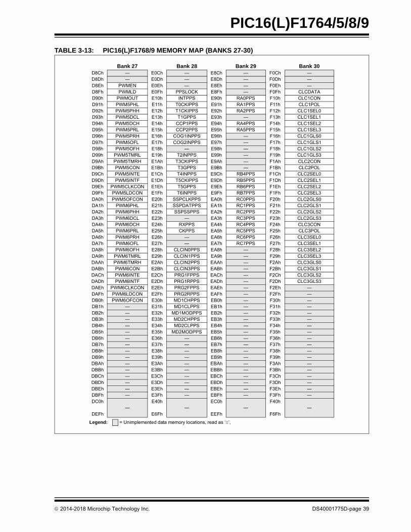
2014-2018 Microchip Technology Inc. DS40001775D-page 39
PIC16(L)F1764/5/8/9
TABLE 3-13: PIC16(L)F1768/9 MEMORY MAP (BANKS 27-30)
Legend: = Unimplemented data memory locations, read as ‘0’,
Bank 27 Bank 28 Bank 29 Bank 30D8Ch — E0Ch — E8Ch — F0Ch —D8Dh — E0Dh — E8Dh — F0Dh —D8Eh PWMEN E0Eh — E8Eh — F0Eh —D8Fh PWMLD E0Fh PPSLOCK E8Fh — F0Fh CLCDATAD90h PWMOUT E10h INTPPS E90h RA0PPS F10h CLC1COND91h PWM5PHL E11h T0CKIPPS E91h RA1PPS F11h CLC1POLD92h PWM5PHH E12h T1CKIPPS E92h RA2PPS F12h CLC1SEL0D93h PWM5DCL E13h T1GPPS E93h — F13h CLC1SEL1D94h PWM5DCH E14h CCP1PPS E94h RA4PPS F14h CLC1SEL2D95h PWM5PRL E15h CCP2PPS E95h RA5PPS F15h CLC1SEL3D96h PWM5PRH E16h COG1INPPS E96h — F16h CLC1GLS0D97h PWM5OFL E17h COG2INPPS E97h — F17h CLC1GLS1D98h PWM5OFH E18h — E98h — F18h CLC1GLS2D99h PWM5TMRL E19h T2INPPS E99h — F19h CLC1GLS3D9Ah PWM5TMRH E1Ah T3CKIPPS E9Ah — F1Ah CLC2COND9Bh PWM5CON E1Bh T3GPPS E9Bh — F1Bh CLC2POLD9Ch PWM5INTE E1Ch T4INPPS E9Ch RB4PPS F1Ch CLC2SEL0D9Dh PWM5INTF E1Dh T5CKIPPS E9Dh RB5PPS F1Dh CLC2SEL1D9Eh PWM5CLKCON E1Eh T5GPPS E9Eh RB6PPS F1Eh CLC2SEL2D9Fh PWM5LDCON E1Fh T6INPPS E9Fh RB7PPS F1Fh CLC2SEL3DA0h PWM5OFCON E20h SSPCLKPPS EA0h RC0PPS F20h CLC2GLS0DA1h PWM6PHL E21h SSPDATPPS EA1h RC1PPS F21h CLC2GLS1DA2h PWM6PHH E22h SSPSSPPS EA2h RC2PPS F22h CLC2GLS2DA3h PWM6DCL E23h — EA3h RC3PPS F23h CLC2GLS3DA4h PWM6DCH E24h RXPPS EA4h RC4PPS F24h CLC3CONDA5h PWM6PRL E25h CKPPS EA5h RC5PPS F25h CLC3POLDA6h PWM6PRH E26h — EA6h RC6PPS F26h CLC3SEL0DA7h PWM6OFL E27h — EA7h RC7PPS F27h CLC3SEL1DA8h PWM6OFH E28h CLCIN0PPS EA8h — F28h CLC3SEL2DA9h PWM6TMRL E29h CLCIN1PPS EA9h — F29h CLC3SEL3DAAh PWM6TMRH E2Ah CLCIN2PPS EAAh — F2Ah CLC3GLS0DABh PWM6CON E2Bh CLCIN3PPS EABh — F2Bh CLC3GLS1DACh PWM6INTE E2Ch PRG1FPPS EACh — F2Ch CLC3GLS2DADh PWM6INTF E2Dh PRG1RPPS EADh — F2Dh CLC3GLS3DAEh PWM6CLKCON E2Eh PRG2FPPS EAEh — F2Eh —DAFh PWM6LDCON E2Fh PRG2RPPS EAFh — F2Fh —DB0h PWM6OFCON E30h MD1CHPPS EB0h — F30h —DB1h — E31h MD1CLPPS EB1h — F31h —DB2h — E32h MD1MODPPS EB2h — F32h —DB3h — E33h MD2CHPPS EB3h — F33h —DB4h — E34h MD2CLPPS EB4h — F34h —DB5h — E35h MD2MODPPS EB5h — F35h —DB6h — E36h — EB6h — F36h —DB7h — E37h — EB7h — F37h —DB8h — E38h — EB8h — F38h —DB9h — E39h — EB9h — F39h —DBAh — E3Ah — EBAh — F3Ah —DBBh — E3Bh — EBBh — F3Bh —DBCh — E3Ch — EBCh — F3Ch —DBDh — E3Dh — EBDh — F3Dh —DBEh — E3Eh — EBEh — F3Eh —DBFh — E3Fh — EBFh — F3Fh —DC0h
—E40h
—EC0h
—F40h
—DEFh E6Fh EEFh F6Fh

2014-2018 Microchip Technology Inc. DS40001775D-page 40
PIC16(L)F1764/5/8/9
TABLE 3-14: PIC16(L)F1764/5/8/9 MEMORY MAP (BANK 31)
Legend: = Unimplemented data memory locations, read as ‘0’,
Bank 31F8Ch
UnimplementedRead as ‘0’
FE3h
FE4h STATUS_SHAD
FE5h WREG_SHAD
FE6h BSR_SHAD
FE7h PCLATH_SHAD
FE8h FSR0L_SHAD
FE9h FSR0H_SHAD
FEAh FSR1L_SHAD
FEBh FSR1H_SHAD
FECh —
FEDh STKPTR
FEEh TOSL
FEFh TOSH
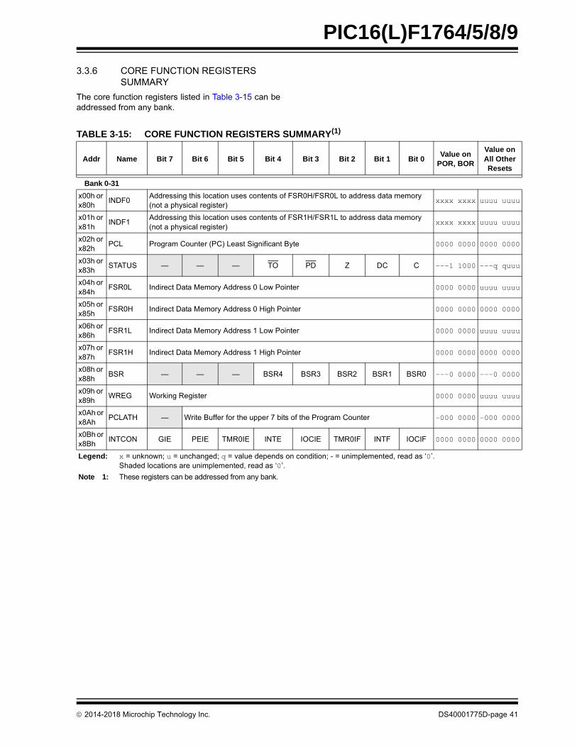
2014-2018 Microchip Technology Inc. DS40001775D-page 41
PIC16(L)F1764/5/8/9
3.3.6 CORE FUNCTION REGISTERS SUMMARY
The core function registers listed in Table 3-15 can beaddressed from any bank.
TABLE 3-15: CORE FUNCTION REGISTERS SUMMARY(1)
Addr Name Bit 7 Bit 6 Bit 5 Bit 4 Bit 3 Bit 2 Bit 1 Bit 0Value on
POR, BOR
Value on All Other Resets
Bank 0-31
x00h or x80h
INDF0Addressing this location uses contents of FSR0H/FSR0L to address data memory(not a physical register)
xxxx xxxx uuuu uuuu
x01h or x81h
INDF1Addressing this location uses contents of FSR1H/FSR1L to address data memory(not a physical register)
xxxx xxxx uuuu uuuu
x02h or x82h
PCL Program Counter (PC) Least Significant Byte 0000 0000 0000 0000
x03h or x83h
STATUS — — — TO PD Z DC C ---1 1000 ---q quuu
x04h or x84h
FSR0L Indirect Data Memory Address 0 Low Pointer 0000 0000 uuuu uuuu
x05h or x85h
FSR0H Indirect Data Memory Address 0 High Pointer 0000 0000 0000 0000
x06h or x86h
FSR1L Indirect Data Memory Address 1 Low Pointer 0000 0000 uuuu uuuu
x07h or x87h
FSR1H Indirect Data Memory Address 1 High Pointer 0000 0000 0000 0000
x08h or x88h
BSR — — — BSR4 BSR3 BSR2 BSR1 BSR0 ---0 0000 ---0 0000
x09h or x89h
WREG Working Register 0000 0000 uuuu uuuu
x0Ah or x8Ah
PCLATH — Write Buffer for the upper 7 bits of the Program Counter -000 0000 -000 0000
x0Bh or x8Bh
INTCON GIE PEIE TMR0IE INTE IOCIE TMR0IF INTF IOCIF 0000 0000 0000 0000
Legend: x = unknown; u = unchanged; q = value depends on condition; - = unimplemented, read as ‘0’. Shaded locations are unimplemented, read as ‘0’.
Note 1: These registers can be addressed from any bank.

2014-2018 Microchip Technology Inc. DS40001775D-page 42
PIC16(L)F1764/5/8/9
TABLE 3-16: SPECIAL FUNCTION REGISTER SUMMARY
Addr Name Bit 7 Bit 6 Bit 5 Bit 4 Bit 3 Bit 2 Bit 1 Bit 0Value on
POR, BOR
Value on All Other Resets
Bank 0
00Ch PORTA — — RA<5:0> --xx xxxx --uu uuuu
00Dh PORTB(2) RB<7:4> — — — — xxxx ---- uuuu ----
00Eh PORTC RC<7:6>(2) RC<5:0> xxxx xxxx uuuu uuuu
00Fh — Unimplemented — —
010h — Unimplemented — —
011h PIR1 TMR1GIF ADIF RCIF TXIF SSP1IF CCP1IF TMR2IF TMR1IF 0000 0000 0000 0000
012h PIR2 OSFIF C2IF C1IF — BCL1IF C4IF(2) C3IF(2) CCP2IF(2) 000- 0000 000- 0000
013h PIR3 PWM6IF(2) PWM5IF COG1IF ZCDIF COG2IF(2) CLC3IF CLC2IF CLC1IF 0000 0000 0000 0000
014h PIR4 — — TMR5GIF TMR5IF TMR3GIF TMR3IF TMR6IF TRM4IF --00 0000 --00 0000
015h TMR0 Timer0 Module Register 0000 0000 0000 0000
016h TMR1L Holding Register for the Least Significant Byte of the 16-Bit TMR1 Register xxxx xxxx uuuu uuuu
017h TMR1H Holding Register for the Most Significant Byte of the 16-Bit TMR1 Register xxxx xxxx uuuu uuuu
018h T1CON CS<1:0> CKPS<1:0> OSCEN SYNC — ON 0000 00-0 uuuu uu-u
019h T1GCON GE GPOL GTM GSPM GGO/DONE GVAL GSS<1:0> 0000 0x00 uuuu uxuu
01Ah T2TMR Holding Register for the 8-Bit TMR2 Register 0000 0000 0000 0000
01Bh T2PR TMR2 Period Register 1111 1111 1111 1111
01Ch T2CON ON CKPS<2:0> OUTPS<3:0> 0000 0000 0000 0000
01Dh T2HLT PSYNC CKPOL CKSYNC MODE<4:0> 0000 0000 0000 0000
01Eh T2CLKCON — — — — CS<3:0> ---- 0000 ---- 0000
01Fh T2RST — — — — RSEL<3:0> ---- 0000 ---- 0000
Bank 1
08Ch TRISA — — TRISA<5:4> —(1) TRISA<2:0> --11 1111 --11 1111
08Dh TRISB(2) TRISB<7:4> — — — — 1111 ---- 1111 ----
08Eh TRISC TRISC<7:6>(2) TRISC<5:0> 1111 1111 1111 1111
08Fh — Unimplemented — —
090h — Unimplemented — —
091h PIE1 TMR1GIE ADIE RCIE TXIE SSP1IE CCP1IE TMR2IE TMR1IE 0000 0000 0000 0000
092h PIE2 OSFIE C2IE C1IE — BCL1IE C4IE(2) C3IE(2) CCP2IE(2) 000- 0000 000- 0000
093h PIE3 PWM6IE(2) PWM5IE COG1IE ZCDIE COG2IE(2) CLC3IE CLC2IE CLC1IE 0000 0000 0000 0000
094h PIE4 — — TMR5GIE TMR5IE TMR3GIE TMR3IE TMR6IE TRM4IE --00 0000 --00 0000
095h OPTION_REG WPUEN INTEDG TMR0CS TMR0SE PSA PS<2:0> 1111 1111 1111 1111
096h PCON STKOVF STKUNF — RWDT RMCLR RI POR BOR 00-1 11qq qq-q qquu
097h WDTCON — — WDTPS<4:0> SWDTEN --01 0110 --01 0110
098h OSCTUNE — — TUN<5:0> --00 0000 --00 0000
099h OSCCON SPLLEN IRCF<3:0> — SCS<1:0> 0011 1-00 0011 1-00
09Ah OSCSTAT SOSCR PLLR OSTS HFIOFR HFIOFL MFIOFR LFIOFR HFIOFS 00q0 0q0q qqqq qq0q
09Bh ADRESL ADC Result Register Low xxxx xxxx uuuu uuuu
09Ch ADRESH ADC Result Register High xxxx xxxx uuuu uuuu
09Dh ADCON0 — CHS<4:0> GO/DONE ADON -000 0000 -000 0000
09Eh ADCON1 ADFM ADCS<2:0> — ADNREF ADPREF<1:0> 0000 -000 0000 -000
09Fh ADCON2 TRIGSEL<4:0> — — — 0000 0--- 0000 0---
Legend: x = unknown; u = unchanged; q = value depends on condition; - = unimplemented, read as ‘0’; r = reserved. Shaded locations are unimplemented, read as ‘0’.
Note 1: Unimplemented, read as ‘1’.2: PIC16(L)F1768/9 only.3: PIC16(L)F1764/5 only.4: Unimplemented on PIC16LF1764/5/8/9.5: PIC16(L)F1768/9 only.

2014-2018 Microchip Technology Inc. DS40001775D-page 43
PIC16(L)F1764/5/8/9
Bank 2
10Ch LATA — — LATA<5:4> — LATA<2:0> --xx -xxx --uu -uuu
10Dh LATB(2) LATB<7:4> — — — — xxxx ---- uuuu ----
10Eh LATC LATC<7:6>(2) LATC<5:0> xxxx xxxx uuuu uuuu
10Fh CMOUT — — — — MC4OUT(2) MC3OUT(2) MC2OUT MC1OUT ---- 0000 ---- 0000
110h CM1CON0 ON OUT — POL ZLF Reserved HYS SYNC 00-0 0100 00-0 0100
111h CM1CON1 — — — — — — INTP INTN ---- --00 ---- --00
112h CM1NSEL — — — — — NCH<2:0> ---- -000 ---- -000
113h CM1PSEL — — — — — PCH<2:0> ---- -000 ---- -000
114h CM2CON0 ON OUT — POL ZLF Reserved HYS SYNC 00-0 0100 00-0 0100
115h CM2CON1 — — — — — — INTP INTN ---- --00 ---- --00
116h CM2NSEL — — — — — NCH<2:0> ---- -000 ---- -000
117h CM2PSEL — — — — — PCH<2:0> ---- -000 ---- -000
118h CM3CON0(2) ON OUT — POL ZLF Reserved HYS SYNC 00-0 0100 00-0 0100
119h CM3CON1(2) — — — — — — INTP INTN ---- --00 ---- --00
11Ah CM3NSEL(2) — — — — — NCH<2:0> ---- -000 ---- -000
11Bh CM3PSEL(2) — — — — — PCH<2:0> ---- -000 ---- -000
11Ch CM4CON0(2) ON OUT — POL ZLF Reserved HYS SYNC 00-0 0100 00-0 0100
11Dh CM4CON1(2) — — — — — — INTP INTN ---- --00 ---- --00
11Eh CM4NSEL(2) — — — — — NCH<2:0> ---- -000 ---- -000
11Fh CM4PSEL(2) — — — — — PCH<2:0> ---- -000 ---- -000
Bank 3
18Ch ANSELA — — — ANSA4 — ANSA<2:0> ---1 -111 ---1 -111
18Dh ANSELB(2) ANSB<7:4> — — — — 1111 ---- 1111 ----
18Eh ANSELC ANSC<7:6>(2) — — ANSC<3:0> 11-- 1111 11-- 1111
18Fh — Unimplemented — —
190h — Unimplemented — —
191h PMADRL Program Memory Address Register Low Byte 0000 0000 0000 0000
192h PMADRH —(1) Program Memory Address Register High Byte 1000 0000 1000 0000
193h PMDATL Program Memory Read Data Register Low Byte xxxx xxxx uuuu uuuu
194h PMDATH — — Program Memory Read Data Register High Byte --xx xxxx --uu uuuu
195h PMCON1 —(1) CFGS LWLO FREE WRERR WREN WR RD 1000 x000 1000 q000
196h PMCON2 Program Memory Control Register 2 0000 0000 0000 0000
197h VREGCON(4) — — — — — — VREGPM Reserved ---- --01 ---- --01
198h — Unimplemented — —
199h RC1REG EUSART Receive Data Register 0000 0000 0000 0000
19Ah TX1REG EUSART Transmit Data Register 0000 0000 0000 0000
19Bh SP1BRGL SP1BRG<7:0> 0000 0000 0000 0000
19Ch SP1BRGH SP1BRG<15:8> 0000 0000 0000 0000
19Dh RC1STA SPEN RX9 SREN CREN ADDEN FERR OERR RX9D 0000 0000 0000 0000
19Eh TX1STA CSRC TX9 TXEN SYNC SENDB BRGH TRMT TX9D 0000 0010 0000 0010
19Fh BAUD1CON ABDOVF RCIDL — SCKP BRG16 — WUE ABDEN 01-0 0-00 01-0 0-00
TABLE 3-16: SPECIAL FUNCTION REGISTER SUMMARY (CONTINUED)
Addr Name Bit 7 Bit 6 Bit 5 Bit 4 Bit 3 Bit 2 Bit 1 Bit 0Value on
POR, BOR
Value on All Other Resets
Legend: x = unknown; u = unchanged; q = value depends on condition; - = unimplemented, read as ‘0’; r = reserved. Shaded locations are unimplemented, read as ‘0’.
Note 1: Unimplemented, read as ‘1’.2: PIC16(L)F1768/9 only.3: PIC16(L)F1764/5 only.4: Unimplemented on PIC16LF1764/5/8/9.5: PIC16(L)F1768/9 only.

2014-2018 Microchip Technology Inc. DS40001775D-page 44
PIC16(L)F1764/5/8/9
Bank 4
20Ch WPUA — — WPUA<5:0 --11 1111 --11 1111
20Dh WPUB(2) WPUB<7:4> — — — — 1111 ---- 1111 ----
20Eh WPUC WPUC<7:6>(2) WPUC<5:0> 1111 1111 1111 1111
20Fh — Unimplemented — —
210h — Unimplemented — —
211h SSP1BUF Synchronous Serial Port Receive Buffer/Transmit Register xxxx xxxx uuuu uuuu
212h SSP1ADD ADD<7:0> 0000 0000 0000 0000
213h SSP1MSK MSK<7:0> 1111 1111 1111 1111
214h SSP1STAT SMP CKE D/A P S R/W UA BF 0000 0000 0000 0000
215h SSP1CON1 WCOL SSPOV SSPEN CKP SSPM<3:0> 0000 0000 0000 0000
216h SSP1CON2 GCEN ACKSTAT ACKDT ACKEN RCEN PEN RSEN SEN 0000 0000 0000 0000
217h SSP1CON3 ACKTIM PCIE SCIE BOEN SDAHT SBCDE AHEN DHEN 0000 0000 0000 0000
218h—
21Ch— Unimplemented — —
21Dh BORCON SBOREN BORFS — — — — — BORRDY 10-- ---q uu-- ---u
21Eh FVRCON FVREN FVRRDY TSEN TSRNG CDAFVR<1:0> ADFVR<1:0> 0q00 0000 0q00 0000
21Fh ZCD1CON EN — OUT POL — — INTP INTN 0-x0 --00 0-x0 --00
Bank 5
28Ch ODCONA — — ODA<5:4> — ODA<2:0> --00 -000 --00 -000
28Dh ODCONB(2) ODB<7:4> — — — — 0000 ---- 0000 ----
28Eh ODCONC ODC<7:6>(2) ODC<5:0> 0000 0000 0000 0000
28Fh — Unimplemented — —
290h — Unimplemented — —
291h CCPR1L Capture/Compare/PWM Register 1 (LSB) xxxx xxxx uuuu uuuu
292h CCPR1H Capture/Compare/PWM Register 1 (MSB) xxxx xxxx uuuu uuuu
293h CCP1CON EN — OUT FMT MODE<3:0> 0-00 0000 0-00 0000
294h CCP1CAP — — — — — CTS<2:0> ---- -000 ---- -000
295h—
297h— Unimplemented — —
298h CCPR2L(2) Capture/Compare/PWM Register 2 (LSB) xxxx xxxx uuuu uuuu
299h CCPR2H(2) Capture/Compare/PWM Register 2 (MSB) xxxx xxxx uuuu uuuu
29Ah CCP2CON(2) EN — OUT FMT MODE<3:0> 0-00 0000 0-00 0000
29Bh CCP2CAP(2) — — — — — CTS<2:0> ---- -000 ---- -000
29Ch—
29Dh— Unimplemented — —
29Eh CCPTMRS P4TSEL<1:0>(2) P3TSEL<1:0> C2TSEL<1:0>(2) C1TSEL<1:0> 0000 0000 0000 0000
29Fh — Unimplemented — —
TABLE 3-16: SPECIAL FUNCTION REGISTER SUMMARY (CONTINUED)
Addr Name Bit 7 Bit 6 Bit 5 Bit 4 Bit 3 Bit 2 Bit 1 Bit 0Value on
POR, BOR
Value on All Other Resets
Legend: x = unknown; u = unchanged; q = value depends on condition; - = unimplemented, read as ‘0’; r = reserved. Shaded locations are unimplemented, read as ‘0’.
Note 1: Unimplemented, read as ‘1’.2: PIC16(L)F1768/9 only.3: PIC16(L)F1764/5 only.4: Unimplemented on PIC16LF1764/5/8/9.5: PIC16(L)F1768/9 only.

2014-2018 Microchip Technology Inc. DS40001775D-page 45
PIC16(L)F1764/5/8/9
Bank 6
30Ch SLRCONA — — SLRA<5:4> — SLRA<2:0> --11 -111 --11 -111
30Dh SLRCONB(2) SLRB<7:4> — — — — 1111 ---- 1111 ----
30Eh SLRCONC SLRC<7:6>(2) SLRC<5:0> 1111 1111 1111 1111
30Fh —31Ah
— Unimplemented — —
31Bh MD2CON0(2) EN — OUT OPOL — — — BIT 0-00 ---0 0-00 ---0
31Ch MD2CON1(2) — — CHPOL CHSYNC — — CLPOL CLSYNC --00 --00 --00 --00
31Dh MD2SRC(2) — — — MS<4:0> ---0 0000 ---0 0000
31Eh MD2CARL(2) — — — — CL<3:0> ---- 0000 ---- 0000
31Fh MD2CARH(2) — — — — CH<3:0> ---- 0000 ---- 0000
Bank 7
38Ch INLVLA — — INLVLA<5:0> --11 1111 --11 1111
38Dh INLVLB(2) INLVLB<7:4> — — — — 1111 ---- 1111 ----
38Eh INLVLC INLVLC<7:6>(2) INLVLC<5:0> 1111 1111 1111 1111
38Fh — Unimplemented — —
390h — Unimplemented — —
391h IOCAP — — IOCAP<5:0> --00 0000 --00 0000
392h IOCAN — — IOCAN<5:0> --00 0000 --00 0000
393h IOCAF — — IOCAF<5:0> --00 0000 --00 0000
394h IOCBP(2) IOCBP<7:4> — — — — 0000 ---- 0000 ----
395h IOCBN(2) IOCBN<7:4> — — — — 0000 ---- 0000 ----
396h IOCBF(2) IOCBF<7:4> — — — — 0000 ---- 0000 ----
397h IOCCP IOCCP<7:6>(2) IOCCP<5:0> 0000 0000 0000 0000
398h IOCCN IOCCN<7:6>(2) IOCCN<5:0> 0000 0000 0000 0000
399h IOCCF IOCCF<7:6>(2) IOCCF<5:0> 0000 0000 0000 0000
39Ah — Unimplemented — —
39Bh MD1CON0 EN — OUT OPOL — — — BIT 0-00 ---0 0-00 ---0
39Ch MD1CON1 — — CHPOL CHSYNC — — CLPOL CLSYNC --00 --00 --00 --00
39Dh MD1SRC — — — MS<4:0> ---0 0000 ---0 0000
39Eh MD1CARL — — — — CL<3:0> ---- 0000 ---- 0000
39Fh MD1CARH — — — — CH<3:0> ---- 0000 ---- 0000
TABLE 3-16: SPECIAL FUNCTION REGISTER SUMMARY (CONTINUED)
Addr Name Bit 7 Bit 6 Bit 5 Bit 4 Bit 3 Bit 2 Bit 1 Bit 0Value on
POR, BOR
Value on All Other Resets
Legend: x = unknown; u = unchanged; q = value depends on condition; - = unimplemented, read as ‘0’; r = reserved. Shaded locations are unimplemented, read as ‘0’.
Note 1: Unimplemented, read as ‘1’.2: PIC16(L)F1768/9 only.3: PIC16(L)F1764/5 only.4: Unimplemented on PIC16LF1764/5/8/9.5: PIC16(L)F1768/9 only.

2014-2018 Microchip Technology Inc. DS40001775D-page 46
PIC16(L)F1764/5/8/9
Bank 8
40Ch —40Dh
— Unimplemented — —
40Eh HIDRVC — — HIDC<5:4> — — — — --00 ---- --00 ----
40Fh —412h
— Unimplemented — —
413h T4TMR Holding Register for the 8-Bit TMR4 Register 0000 0000 0000 0000
413h T4PR TMR4 Period Register 1111 1111 1111 1111
415h T4CON ON CKPS<2:0> OUTPS<3:0> 0000 0000 0000 0000
416h T4HLT PSYNC CKPOL CKSYNC MODE<4:0> 0000 0000 0000 0000
417h T4CLKCON — — — — CS<3:0> ---- 0000 ---- 0000
418h T4RST — — — — RSEL<3:0> ---- 0000 ---- 0000
419h — Unimplemented — —
41Ah T6TMR Holding Register for the 8-Bit TMR4 Register 0000 0000 0000 0000
41Bh T6PR TMR4 Period Register 1111 1111 1111 1111
41Ch T6CON ON CKPS<2:0> OUTPS<3:0> 0000 0000 0000 0000
41Dh T6HLT PSYNC CKPOL CKSYNC MODE<4:0> 0000 0000 0000 0000
41Eh T6CLKCON — — — — CS<3:0> ---- 0000 ---- 0000
41Fh T6RST — — — — RSEL<3:0> ---- 0000 ---- 0000
Bank 9
48Ch to
492h— Unimplemented — —
493h TMR3L Holding Register for the Least Significant Byte of the 16-Bit TMR1 Register xxxx xxxx uuuu uuuu
494h TMR3H Holding Register for the Most Significant Byte of the 16-Bit TMR1 Register xxxx xxxx uuuu uuuu
495h T3CON CS<1:0> CKPS<1:0> OSCEN SYNC — ON 0000 00-0 uuuu uu-u
496h T3GCON GE GPOL GTM GSPM GGO/DONE GVAL GSS<1:0> 0000 0x00 uuuu uxuu
497h to
499h— Unimplemented — —
49Ah TMR5L Holding Register for the Least Significant Byte of the 16-Bit TMR1 Register xxxx xxxx uuuu uuuu
49Bh TMR5H Holding Register for the Most Significant Byte of the 16-Bit TMR1 Register xxxx xxxx uuuu uuuu
49Ch T5CON CS<1:0> CKPS<1:0> OSCEN SYNC — ON 0000 00-0 uuuu uu-u
49Dh T5GCON GE GPOL GTM GSPM GGO/DONE GVAL GSS<1:0> 0000 0x00 uuuu uxuu
49Eh to
49Fh— Unimplemented — —
TABLE 3-16: SPECIAL FUNCTION REGISTER SUMMARY (CONTINUED)
Addr Name Bit 7 Bit 6 Bit 5 Bit 4 Bit 3 Bit 2 Bit 1 Bit 0Value on
POR, BOR
Value on All Other Resets
Legend: x = unknown; u = unchanged; q = value depends on condition; - = unimplemented, read as ‘0’; r = reserved. Shaded locations are unimplemented, read as ‘0’.
Note 1: Unimplemented, read as ‘1’.2: PIC16(L)F1768/9 only.3: PIC16(L)F1764/5 only.4: Unimplemented on PIC16LF1764/5/8/9.5: PIC16(L)F1768/9 only.

2014-2018 Microchip Technology Inc. DS40001775D-page 47
PIC16(L)F1764/5/8/9
Bank 10
50Ch —50Eh
— Unimplemented — —
50Fh OPA1NCHS — — — — NCH<3:0> ---- 0000 ---- 0000
510h OPA1PCHS — — — — PCH<3:0> ---- 0000 ---- 0000
511h OPA1CON EN — — UG — ORPOL ORM<1:0> 0--0 -000 0--0 -000
512h OPA1ORS — — — ORS<4:0> ---0 0000 ---0 0000
513h OPA2NCHS(2) — — — — NCH<3:0> ---- 0000 ---- 0000
514h OPA2PCHS(2) — — — — PCH<3:0> ---- 0000 ---- 0000
515h OPA2CON(2) EN — — UG — ORPOL ORM<1:0> 0--0 -000 0--0 -000
516h OPA2ORS(2) — — — ORS<4:0> ---0 0000 ---0 0000
517h —51Fh
— Unimplemented — —
Bank 11
590h DACLD --- --- --- --- --- --- DAC2LD(2) DAC1LD ---- --00 ---- --00
591h DAC1CON0 EN FM OE1 --- PSS<1:0> NSS<1:0> 000- 0000 000- 0000
592h DAC1REFL REF<7:0> 0000 0000 0000 0000
593h DAC1REFH REF<15:8> 0000 0000 0000 0000
594h DAC2CON0(2) EN FM OE1 --- PSS<1:0> NSS<1:0> 000- 0000 000- 0000
595h DAC2REFL(2) REF<7:0> 0000 0000 0000 0000
596h DAC2REFH(2) REF<15:8> 0000 0000 0000 0000
597h DAC3CON0 EN --- OE1 --- PSS<1:0> NSS<1:0> 0-0- 0000 0-00 0000
598h DAC3REF --- --- --- REF<4:0> ---0 0000 ---0 0000
599h DAC4CON0(2) EN --- OE1 --- PSS<1:0> NSS<1:0> 0-0- 0000 0-00 0000
59Ah DAC4REF(2) --- --- --- REF<4:0> ---0 0000 ---0 0000
59Bh to
59Fh— Unimplemented — —
TABLE 3-16: SPECIAL FUNCTION REGISTER SUMMARY (CONTINUED)
Addr Name Bit 7 Bit 6 Bit 5 Bit 4 Bit 3 Bit 2 Bit 1 Bit 0Value on
POR, BOR
Value on All Other Resets
Legend: x = unknown; u = unchanged; q = value depends on condition; - = unimplemented, read as ‘0’; r = reserved. Shaded locations are unimplemented, read as ‘0’.
Note 1: Unimplemented, read as ‘1’.2: PIC16(L)F1768/9 only.3: PIC16(L)F1764/5 only.4: Unimplemented on PIC16LF1764/5/8/9.5: PIC16(L)F1768/9 only.

2014-2018 Microchip Technology Inc. DS40001775D-page 48
PIC16(L)F1764/5/8/9
Bank 12
60Ch to
616h— Unimplemented — —
617h PWM3DCL DC<1:0> — — — — — — xx-- ---- uu-- ----
618h PWM3DCH DC<9:2> xxxx xxxx uuuu uuuu
619h PWM3CON EN — OUT POL — — — — 0-00 ---- 0-00 ----
61Ah PWM4DCL(2) DC<1:0> — — — — — — 00-- ---- uu-- ----
61Bh PWM4DCH(2) DC<9:2> 0000 0000 uuuu uuuu
61Ch PWM4CON(2) EN — OUT POL — — — — 0-00 ---- 0-00 ----
61Dh—
61Fh— Unimplemented — —
Bank 13
68Ch — Unimplemented — —
68Dh COG1PHR — — COG Rising Edge Phase Delay Count Register --00 0000 --00 0000
68Eh COG1PHF — — COG Falling Edge Phase Delay Count Register --00 0000 --00 0000
68Fh COG1BLKR — — COG Rising Edge Blanking Count Register --00 0000 --00 0000
690h COG1BLKF — — COG Falling Edge Blanking Count Register --00 0000 --00 0000
691h COG1DBR — — COG Rising Edge Dead-band Count Register --00 0000 --00 0000
692h COG1DBF — — COG Falling Edge Dead-band Count Register --00 0000 --00 0000
693h COG1CON0 EN LD — CS<1:0> MD<2:0> 00-0 0000 00-0 0000
694h COG1CON1 RDBS FDBS — — POLD POLC POLB POLA 00-- 0000 00-- 0000
695h COG1RIS0 RIS<7:0> 0000 0000 0000 0000
696h COG1RIS1 RIS15(2) RIS<14:8> 0000 0000 0000 0000
697h COG1RSIM0 RSIM<7:0> 0000 0000 0000 0000
698h COG1RSIM1 RSIM15(2) RSIM<14:8> 0000 0000 0000 0000
699h COG1FIS0 FIS<7:0> 0000 0000 0000 0000
69Ah COG1FIS1 FIS15(2) FIS<14:8> 0000 0000 0000 0000
69Bh COG1FSIM0 FSIM<7:0> 0000 0000 0000 0000
69Ch COG1FSIM1 FSIM15(2) FSIM<14:8> 0000 0000 0000 0000
69Dh COG1ASD0 ASE ARSEN ASDBD<1:0> ASDAC<1:0> — — 0001 01-- 0001 01--
69Eh COG1ASD1 AS7E AS6E AS5E AS4E AS3E AS2E AS1E AS0E 0000 0000 0000 0000
69Fh COG1STR SDATD SDATC SDATB SDATA STRD STRC STRB STRA 0000 0000 0000 0000
TABLE 3-16: SPECIAL FUNCTION REGISTER SUMMARY (CONTINUED)
Addr Name Bit 7 Bit 6 Bit 5 Bit 4 Bit 3 Bit 2 Bit 1 Bit 0Value on
POR, BOR
Value on All Other Resets
Legend: x = unknown; u = unchanged; q = value depends on condition; - = unimplemented, read as ‘0’; r = reserved. Shaded locations are unimplemented, read as ‘0’.
Note 1: Unimplemented, read as ‘1’.2: PIC16(L)F1768/9 only.3: PIC16(L)F1764/5 only.4: Unimplemented on PIC16LF1764/5/8/9.5: PIC16(L)F1768/9 only.

2014-2018 Microchip Technology Inc. DS40001775D-page 49
PIC16(L)F1764/5/8/9
Bank 14
70Ch — Unimplemented — —
70Dh COG2PHR(2) — — COG Rising Edge Phase Delay Count Register --00 0000 --00 0000
70Eh COG2PHF(2) — — COG Falling Edge Phase Delay Count Register --00 0000 --00 0000
70Fh COG2BLKR(2) — — COG Rising Edge Blanking Count Register --00 0000 --00 0000
710h COG2BLKF(2) — — COG Falling Edge Blanking Count Register --00 0000 --00 0000
711h COG2DBR(2) — — COG Rising Edge Dead-band Count Register --00 0000 --00 0000
712h COG2DBF(2) — — COG Falling Edge Dead-band Count Register --00 0000 --00 0000
713h COG2CON0(2) EN LD — CS<1:0> MD<2:0> 00-0 0000 00-0 0000
714h COG2CON1(2) RDBS FDBS — — POLD POLC POLB POLA 00-- 0000 00-- 0000
715h COG2RIS0(2) RIS<7:0> 0000 0000 0000 0000
716h COG2RIS1(2) RIS<15:8> 0000 0000 0000 0000
717h COG2RSIM0(2) RSIM<7:0> 0000 0000 0000 0000
718h COG2RSIM1(2) RSIM<15:8> 0000 0000 0000 0000
719h COG2FIS0(2) FIS<7:0> 0000 0000 0000 0000
71Ah COG2FIS1(2) FIS<15:8> 0000 0000 0000 0000
71Bh COG2FSIM0(2) FSIM<7:0> 0000 0000 0000 0000
71Ch COG2FSIM1(2) FSIM<15:8> 0000 0000 0000 0000
71Dh COG2ASD0(2) ASE ARSEN ASDBD<1:0> ASDAC<1:0> — — 0001 01-- 0001 01--
71Eh COG2ASD1(2) AS7E AS6E AS5E AS4E AS3E AS2E AS1E AS0E 0000 0000 0000 0000
71Fh COG2STR(2) SDATD SDATC SDATB SDATA STRD STRC STRB STRA 0000 0000 0000 0000
Bank 15
78Ch —
793h— Unimplemented — —
794h PRG1RTSS — — — — RTSS<3:0> ---- 0000 ---- 0000
795h PRG1FTSS — — — — FTSS<3:0> ---- 0000 ---- 0000
796h PRG1INS — — — — INS<3:0> ---- 0000 ---- 0000
797h PRG1CON0 EN — FEDG REDG MODE<1:0> OS GO 0-00 0000 0-00 0000
798h PRG1CON1 — — — — — RDY FPOL RPOL ---- -000 ---- -000
799h PRG1CON2 LR(5) — — ISET<4:0> 0--0 0000 0--0 0000
79Ah PRG2RTSS(2) — — — — RTSS<3:0> ---- 0000 ---- 0000
79Bh PRG2FTSS(2) — — — — FTSS<3:0> ---- 0000 ---- 0000
79Ch PRG2INS(2) — — — — INS<3:0> ---- 0000 ---- 0000
79Dh PRG2CON0(2) EN — FEDG REDG MODE<1:0> OS GO 0-00 0000 0-00 0000
79Eh PRG2CON1(2) — — — — — RDY FPOL RPOL ---- -000 ---- -000
79Fh PRG2CON2(2) LR(5) — — ISET<4:0> 0--0 0000 0--0 0000
Bank 16-26
x0Ch/x8Ch —x1Fh/x9Fh
— Unimplemented — —
TABLE 3-16: SPECIAL FUNCTION REGISTER SUMMARY (CONTINUED)
Addr Name Bit 7 Bit 6 Bit 5 Bit 4 Bit 3 Bit 2 Bit 1 Bit 0Value on
POR, BOR
Value on All Other Resets
Legend: x = unknown; u = unchanged; q = value depends on condition; - = unimplemented, read as ‘0’; r = reserved. Shaded locations are unimplemented, read as ‘0’.
Note 1: Unimplemented, read as ‘1’.2: PIC16(L)F1768/9 only.3: PIC16(L)F1764/5 only.4: Unimplemented on PIC16LF1764/5/8/9.5: PIC16(L)F1768/9 only.

2014-2018 Microchip Technology Inc. DS40001775D-page 50
PIC16(L)F1764/5/8/9
Bank 27
D8Ch —D8Dh
— Unimplemented — —
D8Eh PWMEN — — MPWM6EN(2) MPWM5EN — — — — --00 ---- --00 ----
D8Fh PWMLD — — MPWM6LD(2) MPWM5LD — — — — --00 ---- --00 ----
D90h PWMOUT — — MPWM6OUT(2) MPWM5OUT — — — — --00 ---- --00 ----
D91h PWM5PHL PH<7:0> xxxx xxxx uuuu uuuu
D92h PWM5PHH PH<15:8> xxxx xxxx uuuu uuuu
D93h PWM5DCL DC<7:0> xxxx xxxx uuuu uuuu
D94h PWM5DCH DC<15:8> xxxx xxxx uuuu uuuu
D95h PWM5PRL PR<7:0> xxxx xxxx uuuu uuuu
D96h PWM5PRH PR<15:8> xxxx xxxx uuuu uuuu
D97h PWM5OFL OF<7:0> xxxx xxxx uuuu uuuu
D98h PWM5OFH OF<15:8> xxxx xxxx uuuu uuuu
D99h PWM5TMRL TMR<7:0> 0000 0000 0000 0000
D9Ah PWM5TMRH TMR<15:8> 0000 0000 0000 0000
D9Bh PWM5CON EN — OUT POL MODE<1:0> — — 0-00 00-- 0-00 00--
D9Ch PWM5INTE — — — — OFIE PHIE DCIE PRIE ---- 0000 ---- 0000
D9Dh PWM5INTF — — — — OFIF PHIF DCIF PRIF ---- 0000 ---- 0000
D9Eh PWM5CLKCON — PS<2:0> — — CS<1:0> -000 --00 -000 --00
D9Fh PWM5LDCON LDA LDT(2) — — — — — LDS(2) 00-- ---0 00-- ---0
DA0h PWM5OFCON — OFM<1:0>(2) OFO — — — OFS(2) -000 ---0 -000 ---0
DA1h PWM6PHL(2) PH<7:0> xxxx xxxx uuuu uuuu
DA2h PWM6PHH(2) PH<15:8> xxxx xxxx uuuu uuuu
DA3h PWM6DCL(2) DC<7:0> xxxx xxxx uuuu uuuu
DA4h PWM6DCH(2) DC<15:8> xxxx xxxx uuuu uuuu
DA5h PWM6PRL(2) PR<7:0> xxxx xxxx uuuu uuuu
DA6h PWM6PRH(2) PR<15:8> xxxx xxxx uuuu uuuu
DA7h PWM6OFL(2) OF<7:0> xxxx xxxx uuuu uuuu
DA8h PWM6OFH(2) OF<15:8> xxxx xxxx uuuu uuuu
DA9h PWM6TMRL(2) TMR<7:0> 0000 0000 0000 0000
DAAh PWM6TMRH(2) TMR<15:8> 0000 0000 0000 0000
DABh PWM6CON(2) EN — OUT POL MODE<1:0> — — 0-00 00-- 0-00 00--
DACh PWM6INTE(2) — — — — OFIE PHIE DCIE PRIE ---- 0000 ---- 0000
DADh PWM6INTF(2) — — — — OFIF PHIF DCIF PRIF ---- 0000 ---- 0000
DAEh PWM6CLKCON(2) — PS<2:0> — — CS<1:0> -000 --00 -000 --00
DAFh PWM6LDCON(2) LDA LDT — — — — — LDS 00-- ---0 00-- ---0
DB0h PWM6OFCON(2) — OFM<1:0> OFO — — — OFS -000 ---0 -000 ---0
DB1h to
DBFh— Unimplemented — —
TABLE 3-16: SPECIAL FUNCTION REGISTER SUMMARY (CONTINUED)
Addr Name Bit 7 Bit 6 Bit 5 Bit 4 Bit 3 Bit 2 Bit 1 Bit 0Value on
POR, BOR
Value on All Other Resets
Legend: x = unknown; u = unchanged; q = value depends on condition; - = unimplemented, read as ‘0’; r = reserved. Shaded locations are unimplemented, read as ‘0’.
Note 1: Unimplemented, read as ‘1’.2: PIC16(L)F1768/9 only.3: PIC16(L)F1764/5 only.4: Unimplemented on PIC16LF1764/5/8/9.5: PIC16(L)F1768/9 only.

2014-2018 Microchip Technology Inc. DS40001775D-page 51
PIC16(L)F1764/5/8/9
Bank 28
E0Ch —E0Eh
— Unimplemented — —
E0Fh PPSLOCK — — — — — — — PPSLOCKED ---- ---0 ---- ---0
E10h INTPPS — — — INTPPS<4:0> ---0 0010 ---u uuuu
E11h T0CKIPPS — — — T0CKIPPS<4:0> ---0 0010 ---u uuuu
E12h T1CKIPPS — — — T1CKIPPS<4:0> ---0 0101 ---u uuuu
E13h T1GPPS — — — T1GPPS<4:0> ---0 0100 ---u uuuu
E14h CCP1PPS — — — CCP1PPS<4:0> ---1 0101 ---u uuuu
E15h CCP2PPS(2) — — — CCP2PPS<4:0> ---1 0011 ---u uuuu
E16h COG1INPPS — — — COG1INPPS<4:0> ---0 0010 ---u uuuu
E17h COG2INPPS(2) — — — COG2INPPS<4:0> ---0 0010 ---u uuuu
E18h — Unimplemented — —
E19h T2INPPS — — — T2INPPS<4:0> ---0 0101 ---u uuuu
E1Ah T3CKIPPS — — — T3CKIPPS<4:0> ---1 0101 ---u uuuu
E1Bh T3GPPS — — — T3GPPS<4:0> ---1 0100 ---u uuuu
E1Ch T4INPPS — — — T4INPPS<4:0> ---1 0001 ---u uuuu
E1Dh T5CKIPPS — — — T5CKIPPS<4:0> ---1 0000 ---u uuuu
E1Eh T5GPPS — — — T5GPPS<4:0> ---1 0011 ---u uuuu
E1Fh T6INPPS — — — T6INPPS<4:0> ---0 0011 ---u uuuu
E20h SSPCLKPPS— — — SSPCLKPPS<4:0> ---1 0000(3) ---u uuuu
— — — SSPCLKPPS<4:0> ---0 1110(2) ---u uuuu
E21h SSPDATPPS— — — SSPDATPPS<4:0> ---1 0001(3) ---u uuuu
— — — SSPDATPPS<4:0> ---0 1100(2) ---u uuuu
E22h SSPSSPPS— — — SSPSSPPS<4:0> ---1 0011(3) ---u uuuu
— — — SSPSSPPS<4:0> ---1 0110(2) ---u uuuu
E23h — Unimplemented — —
E24h RXPPS— — — RXPPS<4:0> ---1 0101(3) ---u uuuu
— — — RXPPS<4:0> ---0 1101(2) ---u uuuu
E25h CKPPS— — — CKPPS<4:0> ---1 0100(3) ---u uuuu
— — — CKPPS<4:0> ---0 1111(2) ---u uuuu
E26h — Unimplemented — —
E27h — Unimplemented — —
E28h CLCIN0PPS — — — CLCIN0PPS<4:0> ---1 0011 ---u uuuu
E29h CLCIN1PPS — — — CLCIN1PPS<4:0> ---1 0100 ---u uuuu
E2Ah CLCIN2PPS — — — CLCIN2PPS<4:0> ---1 0001 ---u uuuu
E2Bh CLCIN3PPS — — — CLCIN3PPS<4:0> ---0 0101 ---u uuuu
E2Ch PRG1RPPS — — — PRG1RPPS<4:0> ---1 0100 ---u uuuu
E2Dh PRG1FPPS — — — PRG1FPPS<4:0> ---1 0101 ---u uuuu
E2Eh PRG2RPPS(2) — — — PRG2RPPS<4:0> ---1 0100 ---u uuuu
E2Fh PRG2FPPS(2) — — — PRG2FPPS<4:0> ---1 0101 ---u uuuu
E30h MD1CHPPS — — — MD1CHPPS<4:0> ---0 0011 ---u uuuu
E31h MD1CLPPS — — — MD1CLPPS<4:0> ---0 0100 ---u uuuu
TABLE 3-16: SPECIAL FUNCTION REGISTER SUMMARY (CONTINUED)
Addr Name Bit 7 Bit 6 Bit 5 Bit 4 Bit 3 Bit 2 Bit 1 Bit 0Value on
POR, BOR
Value on All Other Resets
Legend: x = unknown; u = unchanged; q = value depends on condition; - = unimplemented, read as ‘0’; r = reserved. Shaded locations are unimplemented, read as ‘0’.
Note 1: Unimplemented, read as ‘1’.2: PIC16(L)F1768/9 only.3: PIC16(L)F1764/5 only.4: Unimplemented on PIC16LF1764/5/8/9.5: PIC16(L)F1768/9 only.

2014-2018 Microchip Technology Inc. DS40001775D-page 52
PIC16(L)F1764/5/8/9
Bank 28 (Continued)
E32h MD1MODPPS — — — MD1MODPPS<4:0> ---0 0101 ---u uuuu
E33h MD2CHPPS(2) — — — MD2CHPPS<4:0> ---0 0011 ---u uuuu
E34h MD2CLPPS(2) — — — MD2CLPPS<4:0> ---0 0100 ---u uuuu
E35h MD2MODPPS(2) — — — MD2MODPPS<4:0> ---0 0101 ---u uuuu
E36h to
E7Fh— Unimplemented — —
Bank 29
E8Ch —E8Fh
— Unimplemented — —
E90h RA0PPS — — — RA0PPS<4:0> ---0 0000 ---u uuuu
E91h RA1PPS — — — RA1PPS<4:0> ---0 0000 ---u uuuu
E92h RA2PPS — — — RA2PPS<4:0> ---0 0000 ---u uuuu
E93h — Unimplemented — —
E94h RA4PPS — — — RA4PPS<4:0> ---0 0000 ---u uuuu
E95h RA5PPS — — — RA5PPS<4:0> ---0 0000 ---u uuuu
E96h — Unimplemented — —
E97h — Unimplemented — —
E98h — Unimplemented — —
E99h — Unimplemented — —
E9Ah — Unimplemented — —
E9Bh — Unimplemented — —
E9Ch RB4PPS(2) — — — RB4PPS<4:0> ---0 0000 ---u uuuu
E9Dh RB5PPS(2) — — — RB5PPS<4:0> ---0 0000 ---u uuuu
E9Eh RB6PPS(2) — — — RB6PPS<4:0> ---0 0000 ---u uuuu
E9Fh RB7PPS(2) — — — RB7PPS<4:0> ---0 0000 ---u uuuu
EA0h RC0PPS — — — RC0PPS<4:0> ---0 0000 ---u uuuu
EA1h RC1PPS — — — RC1PPS<4:0> ---0 0000 ---u uuuu
EA2h RC2PPS — — — RC2PPS<4:0> ---0 0000 ---u uuuu
EA3h RC3PPS — — — RC3PPS<4:0> ---0 0000 ---u uuuu
EA4h RC4PPS — — — RC4PPS<4:0> ---0 0000 ---u uuuu
EA5h RC5PPS — — — RC5PPS<4:0> ---0 0000 ---u uuuu
EA6h RC6PPS(2) — — — RC6PPS<4:0> ---0 0000 ---u uuuu
EA7h RC7PPS(2) — — — RC7PPS<4:0> ---0 0000 ---u uuuu
EA8h —EEFh
— Unimplemented — —
TABLE 3-16: SPECIAL FUNCTION REGISTER SUMMARY (CONTINUED)
Addr Name Bit 7 Bit 6 Bit 5 Bit 4 Bit 3 Bit 2 Bit 1 Bit 0Value on
POR, BOR
Value on All Other Resets
Legend: x = unknown; u = unchanged; q = value depends on condition; - = unimplemented, read as ‘0’; r = reserved. Shaded locations are unimplemented, read as ‘0’.
Note 1: Unimplemented, read as ‘1’.2: PIC16(L)F1768/9 only.3: PIC16(L)F1764/5 only.4: Unimplemented on PIC16LF1764/5/8/9.5: PIC16(L)F1768/9 only.

2014-2018 Microchip Technology Inc. DS40001775D-page 53
PIC16(L)F1764/5/8/9
Bank 30
F0Ch —F0Eh
— Unimplemented — —
F0Fh CLCDATA — — — — — MLC3OUT MLC2OUT MLC1OUT ---- -000 ---- -000
F10h CLC1CON EN — OUT INTP INTN MODE<2:0> 0-00 0000 0-00 0000
F11h CLC1POL POL — — — G4POL G3POL G2POL G1POL 0--- xxxx 0--- uuuu
F12h CLC1SEL0 — — — D1S<4:0> ---x xxxx ---u uuuu
F13h CLC1SEL1 — — — D2S<4:0> ---x xxxx ---u uuuu
F14h CLC1SEL2 — — — D3S<4:0> ---x xxxx ---u uuuu
F15h CLC1SEL3 — — — D4S<4:0> ---x xxxx ---u uuuu
F16h CLC1GLS0 G1D4T G1D4N G1D3T G1D3N G1D2T G1D2N G1D1T G1D1N xxxx xxxx uuuu uuuu
F17h CLC1GLS1 G2D4T G2D4N G2D3T G2D3N G2D2T G2D2N G2D1T G2D1N xxxx xxxx uuuu uuuu
F18h CLC1GLS2 G3D4T G3D4N G3D3T G3D3N G3D2T G3D2N G3D1T G3D1N xxxx xxxx uuuu uuuu
F19h CLC1GLS3 G4D4T G4D4N G4D3T G4D3N G4D2T G4D2N G4D1T G4D1N xxxx xxxx uuuu uuuu
F1Ah CLC2CON EN — OUT INTP INTN MODE<2:0> 0-00 0000 0-00 0000
F1Bh CLC2POL POL — — — G4POL G3POL G2POL G1POL 0--- xxxx 0--- uuuu
F1Ch CLC2SEL0 — — — D1S<4:0> ---x xxxx ---u uuuu
F1Dh CLC2SEL1 — — — D2S<4:0> ---x xxxx ---u uuuu
F1Eh CLC2SEL2 — — — D3S<4:0> ---x xxxx ---u uuuu
F1Fh CLC2SEL3 — — — D4S<4:0> ---x xxxx ---u uuuu
F20h CLC2GLS0 G1D4T G1D4N G1D3T G1D3N G1D2T G1D2N G1D1T G1D1N xxxx xxxx uuuu uuuu
F21h CLC2GLS1 G2D4T G2D4N G2D3T G2D3N G2D2T G2D2N G2D1T G2D1N xxxx xxxx uuuu uuuu
F22h CLC2GLS2 G3D4T G3D4N G3D3T G3D3N G3D2T G3D2N G3D1T G3D1N xxxx xxxx uuuu uuuu
F23h CLC2GLS3 G4D4T G4D4N G4D3T G4D3N G4D2T G4D2N G4D1T G4D1N xxxx xxxx uuuu uuuu
F24h CLC3CON EN — OUT INTP INTN MODE<2:0> 0-00 0000 0-00 0000
F25h CLC3POL POL — — — G4POL G3POL G2POL G1POL 0--- xxxx 0--- uuuu
F26h CLC3SEL0 — — — D1S<4:0> ---x xxxx ---u uuuu
F27h CLC3SEL1 — — — D2S<4:0> ---x xxxx ---u uuuu
F28h CLC3SEL2 — — — D3S<4:0> ---x xxxx ---u uuuu
F29h CLC3SEL3 — — — D4S<4:0> ---x xxxx ---u uuuu
F2Ah CLC3GLS0 G1D4T G1D4N G1D3T G1D3N G1D2T G1D2N G1D1T G1D1N xxxx xxxx uuuu uuuu
F2Bh CLC3GLS1 G2D4T G2D4N G2D3T G2D3N G2D2T G2D2N G2D1T G2D1N xxxx xxxx uuuu uuuu
F2Ch CLC3GLS2 G3D4T G3D4N G3D3T G3D3N G3D2T G3D2N G3D1T G3D1N xxxx xxxx uuuu uuuu
F2Dh CLC3GLS3 G4D4T G4D4N G4D3T G4D3N G4D2T G4D2N G4D1T G4D1N xxxx xxxx uuuu uuuu
F2Eh —F6Fh
— Unimplemented — —
TABLE 3-16: SPECIAL FUNCTION REGISTER SUMMARY (CONTINUED)
Addr Name Bit 7 Bit 6 Bit 5 Bit 4 Bit 3 Bit 2 Bit 1 Bit 0Value on
POR, BOR
Value on All Other Resets
Legend: x = unknown; u = unchanged; q = value depends on condition; - = unimplemented, read as ‘0’; r = reserved. Shaded locations are unimplemented, read as ‘0’.
Note 1: Unimplemented, read as ‘1’.2: PIC16(L)F1768/9 only.3: PIC16(L)F1764/5 only.4: Unimplemented on PIC16LF1764/5/8/9.5: PIC16(L)F1768/9 only.

2014-2018 Microchip Technology Inc. DS40001775D-page 54
PIC16(L)F1764/5/8/9
Bank 31
F8Chto
FE3h— Unimplemented — —
FE4h STATUS_SHAD
— — — — — Z DC C ---- -xxx ---- -uuu
FE5h WREG_SHAD
Working Register Shadow xxxx xxxx uuuu uuuu
FE6h BSR_SHAD — — — Bank Select Register Shadow ---x xxxx ---u uuuu
FE7h PCLATH_SHAD
— Program Counter Latch High Register Shadow -xxx xxxx -uuu uuuu
FE8h FSR0L_SHAD
Indirect Data Memory Address 0 Low Pointer Shadow xxxx xxxx uuuu uuuu
FE9h FSR0H_SHAD
Indirect Data Memory Address 0 High Pointer Shadow xxxx xxxx uuuu uuuu
FEAh FSR1L_SHAD
Indirect Data Memory Address 1 Low Pointer Shadow xxxx xxxx uuuu uuuu
FEBh FSR1H_SHAD
Indirect Data Memory Address 1 High Pointer Shadow xxxx xxxx uuuu uuuu
FECh — Unimplemented — —
FEDh STKPTR — — — Current Stack Pointer ---1 1111 ---1 1111
FEEh TOSL Top of Stack Low byte xxxx xxxx uuuu uuuu
FEFh TOSH — Top of Stack High Byte -xxx xxxx -uuu uuuu
TABLE 3-16: SPECIAL FUNCTION REGISTER SUMMARY (CONTINUED)
Addr Name Bit 7 Bit 6 Bit 5 Bit 4 Bit 3 Bit 2 Bit 1 Bit 0Value on
POR, BOR
Value on All Other Resets
Legend: x = unknown; u = unchanged; q = value depends on condition; - = unimplemented, read as ‘0’; r = reserved. Shaded locations are unimplemented, read as ‘0’.
Note 1: Unimplemented, read as ‘1’.2: PIC16(L)F1768/9 only.3: PIC16(L)F1764/5 only.4: Unimplemented on PIC16LF1764/5/8/9.5: PIC16(L)F1768/9 only.

2014-2018 Microchip Technology Inc. DS40001775D-page 55
PIC16(L)F1764/5/8/9
3.4 PCL and PCLATH
The Program Counter (PC) is 15 bits wide. The low bytecomes from the PCL register, which is a readable andwritable register. The high byte (PC<14:8>) is not directlyreadable or writable and comes from PCLATH. On anyReset, the PC is cleared. Figure 3-3 shows the fivesituations for the loading of the PC.
FIGURE 3-3: LOADING OF PC IN DIFFERENT SITUATIONS
3.4.1 MODIFYING PCL
Executing any instruction with the PCL register as thedestination simultaneously causes the ProgramCounter PC<14:8> bits (PCH) to be replaced by thecontents of the PCLATH register. This allows the entirecontents of the Program Counter to be changed bywriting the desired upper seven bits to the PCLATHregister. When the lower eight bits are written to thePCL register, all 15 bits of the Program Counter willchange to the values contained in the PCLATH registerand those being written to the PCL register.
3.4.2 COMPUTED GOTO
A computed GOTO is accomplished by adding an offset tothe Program Counter (ADDWF PCL). When performing atable read using a computed GOTO method, care shouldbe exercised if the table location crosses a PCL memoryboundary (each 256-byte block). Refer to ApplicationNote AN556, “Implementing a Table Read” (DS00556).
3.4.3 COMPUTED FUNCTION CALLS
A computed function CALL allows programs to maintaintables of functions and provide another way to executestate machines or look-up tables. When performing atable read using a computed function CALL, careshould be exercised if the table location crosses a PCLmemory boundary (each 256-byte block).
If using the CALL instruction, the PCH<2:0> and PCLregisters are loaded with the operand of the CALLinstruction. PCH<6:3> is loaded with PCLATH<6:3>.
The CALLW instruction enables computed calls by com-bining PCLATH and W to form the destination address.A computed CALLW is accomplished by loading the Wregister with the desired address and executing CALLW.The PCL register is loaded with the value of W andPCH is loaded with PCLATH.
3.4.4 BRANCHING
The branching instructions add an offset to the PC.This allows relocatable code and code that crossespage boundaries. There are two forms of branching,BRW and BRA. The PC will have incremented to fetchthe next instruction in both cases. When using eitherbranching instruction, a PCL memory boundary may becrossed.
If using BRW, load the W register with the desiredunsigned address and execute BRW. The entire PC willbe loaded with the address PC + 1 + W.
If using BRA, the entire PC will be loaded with PC + 1 +,the signed value of the operand of the BRA instruction.
PCLPCH 014PC
06 7
ALU Result
8
PCLATH
PCLPCH 014PC
06 4
OPCODE <10:0>11
PCLATH
PCLPCH 014PC
06 7
W8
PCLATH
Instruction with PCL as
Destination
GOTO, CALL
CALLW
PCLPCH 014PC
PC + W15
BRW
PCLPCH 014PC
PC + OPCODE <8:0>15
BRA

2014-2018 Microchip Technology Inc. DS40001775D-page 56
PIC16(L)F1764/5/8/9
3.5 Stack
All devices have a 16-level x 15-bit wide hardwarestack (refer to Figure 3-1). The stack space is not partof either program or data space. The PC is PUSHedonto the stack when CALL or CALLW instructions areexecuted or an interrupt causes a branch. The stack isPOPed in the event of a RETURN, RETLW or a RETFIEinstruction execution. PCLATH is not affected by aPUSH or POP operation.
The stack operates as a circular buffer if the STVRENbit is programmed to ‘0’ (Configuration Words). Thismeans that after the stack has been PUSHed sixteentimes, the seventeenth PUSH overwrites the value thatwas stored from the first PUSH. The eighteenth PUSHoverwrites the second PUSH (and so on). TheSTKOVF and STKUNF flag bits will be set on an Over-flow/Underflow Reset, regardless of whether the Resetis enabled.
3.5.1 ACCESSING THE STACK
The stack is available through the TOSH, TOSL andSTKPTR registers. STKPTR is the current value of theStack Pointer. TOSH:TOSL register pair points to theTOP of the stack. Both registers are read/writable. TOSis split into TOSH and TOSL due to the 15-bit size of thePC. To access the stack, adjust the value of STKPTR,which will position TOSH:TOSL, then read/write toTOSH:TOSL. STKPTR is five bits to allow detection ofoverflow and underflow.
During normal program operation, CALL, CALLW andInterrupts will increment STKPTR while RETLW,RETURN, and RETFIE will decrement STKPTR. At anytime, STKPTR can be inspected to see how muchstack is left. The STKPTR always points at the currentlyused place on the stack. Therefore, a CALL or CALLWwill increment the STKPTR and then write the PC, anda return will unload the PC and then decrement theSTKPTR.
Reference Figure 3-4 through Figure 3-7 for examplesof accessing the stack.
FIGURE 3-4: ACCESSING THE STACK EXAMPLE 1
Note: There are no instructions/mnemonicscalled PUSH or POP. These are actionsthat occur from the execution of the CALL,CALLW, RETURN, RETLW and RETFIEinstructions or the vectoring to an interruptaddress.
Note: Care should be taken when modifying theSTKPTR while interrupts are enabled.
STKPTR = 0x1FStack Reset Disabled(STVREN = 0)
Stack Reset Enabled(STVREN = 1)
Initial Stack Configuration:
After Reset, the stack is empty. Theempty stack is initialized so the StackPointer is pointing at 0x1F. If the StackOverflow/Underflow Reset is enabled, theTOSH/TOSL register will return ‘0’. If theStack Overflow/Underflow Reset isdisabled, the TOSH/TOSL register willreturn the contents of stack address0x0F.
0x0000 STKPTR = 0x1F
TOSH:TOSL 0x0F
0x0E
0x0D
0x0C
0x0B
0x0A
0x09
0x08
0x07
0x06
0x04
0x05
0x03
0x02
0x01
0x00
0x1FTOSH:TOSL
Rev. 10-000043A7/30/2013
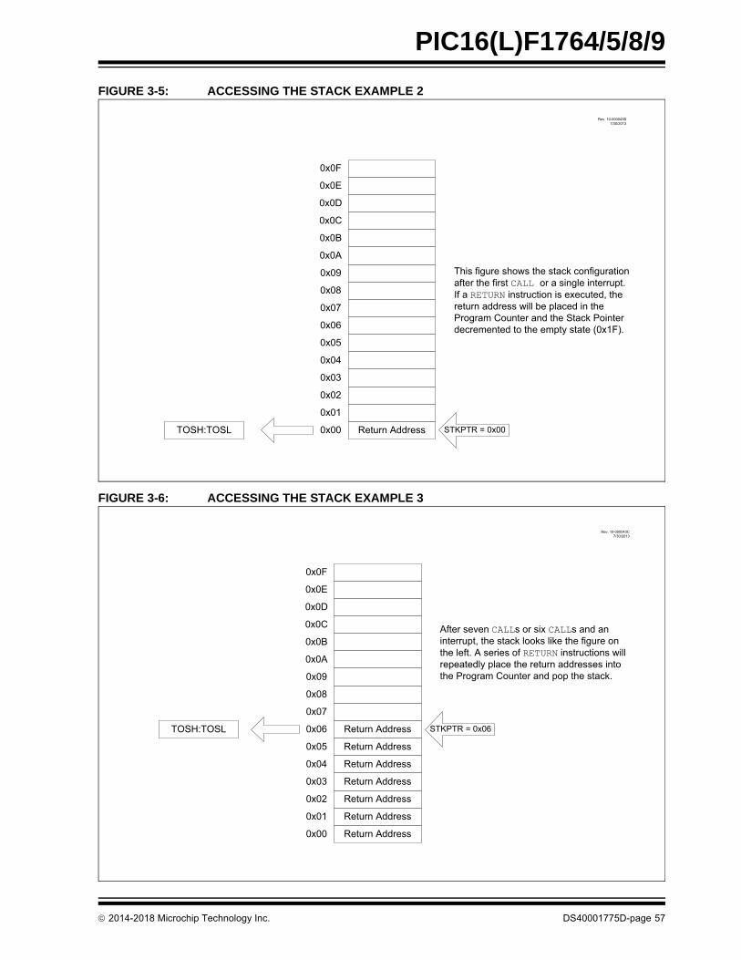
2014-2018 Microchip Technology Inc. DS40001775D-page 57
PIC16(L)F1764/5/8/9
FIGURE 3-5: ACCESSING THE STACK EXAMPLE 2
FIGURE 3-6: ACCESSING THE STACK EXAMPLE 3
STKPTR = 0x00Return Address
This figure shows the stack configurationafter the first CALL or a single interrupt.If a RETURN instruction is executed, thereturn address will be placed in theProgram Counter and the Stack Pointerdecremented to the empty state (0x1F).
0x0F
0x0E
0x0D
0x0C
0x0B
0x0A
0x09
0x08
0x07
0x06
0x04
0x05
0x03
0x02
0x01
0x00TOSH:TOSL
Rev. 10-000043B7/30/2013
STKPTR = 0x06
After seven CALLs or six CALLs and aninterrupt, the stack looks like the figure onthe left. A series of RETURN instructions willrepeatedly place the return addresses intothe Program Counter and pop the stack.
Return Address
0x0F
0x0E
0x0D
0x0C
0x0B
0x0A
0x09
0x08
0x07
0x06
0x04
0x05
0x03
0x02
0x01
0x00
Return Address
Return Address
Return Address
Return Address
Return Address
Return Address
TOSH:TOSL
Rev. 10-000043C7/30/2013

2014-2018 Microchip Technology Inc. DS40001775D-page 58
PIC16(L)F1764/5/8/9
FIGURE 3-7: ACCESSING THE STACK EXAMPLE 4
3.5.2 OVERFLOW/UNDERFLOW RESET
If the STVREN bit in Configuration Words isprogrammed to ‘1’, the device will be reset if the stackis PUSHed beyond the sixteenth level or POPedbeyond the first level, setting the appropriate bits(STKOVF or STKUNF, respectively) in the PCONregister.
3.6 Indirect Addressing
The INDFn registers are not physical registers. Anyinstruction that accesses an INDFn register actuallyaccesses the register at the address specified by theFile Select Registers (FSRs). If the FSRn addressspecifies one of the two INDFn registers, the read willreturn ‘0’ and the write will not occur (though Status bitsmay be affected). The FSRn register value is createdby the pair, FSRnH and FSRnL.
The FSRn registers form a 16-bit address that allows anaddressing space with 65536 locations. These locationsare divided into three memory regions:
• Traditional Data Memory• Linear Data Memory• Program Flash Memory
STKPTR = 0x10
When the stack is full, the next CALL oran interrupt will set the Stack Pointer to0x10. This is identical to address 0x00 sothe stack will wrap and overwrite thereturn address at 0x00. If the StackOverflow/Underflow Reset is enabled, aReset will occur and location 0x00 willnot be overwritten.
Return Address0x0F
0x0E
0x0D
0x0C
0x0B
0x0A
0x09
0x08
0x07
0x06
0x04
0x05
0x03
0x02
0x01
0x00
Return Address
Return Address
Return Address
Return Address
Return Address
Return Address
Return Address
Return Address
Return Address
Return Address
Return Address
Return Address
Return Address
Return Address
Return AddressTOSH:TOSL
Rev. 10-000043D7/30/2013

2014-2018 Microchip Technology Inc. DS40001775D-page 59
PIC16(L)F1764/5/8/9
FIGURE 3-8: INDIRECT ADDRESSING
0x0000
0x0FFF
0x0000
0x7FFF0xFFFF
0x0000
0x0FFF0x1000
0x1FFF0x2000
0x29AF0x29B0
0x7FFF0x8000
Reserved
Reserved
TraditionalData Memory
LinearData Memory
ProgramFlash Memory
FSRAddressRange
Note: Not all memory regions are completely implemented. Consult device memory tables for memory limits.
Rev. 10-000044A7/30/2013

2014-2018 Microchip Technology Inc. DS40001775D-page 60
PIC16(L)F1764/5/8/9
3.6.1 TRADITIONAL DATA MEMORY
The traditional data memory is a region from FSRnaddress, 0x000, to FSRn address, 0xFFF. Theaddresses correspond to the absolute addresses of allSFRs, GPRs and common registers.
FIGURE 3-9: TRADITIONAL DATA MEMORY MAP
Direct Addressing
4 0BSR 6 0From Opcode
007 FSRxH
0 0 007 FSRxL
Indirect Addressing
00000 00001 00010 11111
Bank Select Location Select
0x00
0x7F
Bank Select Location Select
Bank 0 Bank 1 Bank 2 Bank 31
Rev. 10-000056A7/31/2013

2014-2018 Microchip Technology Inc. DS40001775D-page 61
PIC16(L)F1764/5/8/9
3.6.2 LINEAR DATA MEMORY
The linear data memory is the region from FSRnaddress, 0x2000, to FSRn address, 0x29AF. Thisregion is a virtual region that points back to the 80-byteblocks of GPR memory in all the banks.
Unimplemented memory reads as 0x00. Use of thelinear data memory region allows buffers to be largerthan 80 bytes because incrementing the FSRn beyondone bank will go directly to the GPR memory of the nextbank.
The 16 bytes of common memory are not included inthe linear data memory region.
FIGURE 3-10: LINEAR DATA MEMORY MAP
3.6.3 PROGRAM FLASH MEMORY
To make constant data access easier, the entireProgram Flash Memory is mapped to the upper half ofthe FSRn address space. When the MSB of FSRnH isset, the lower 15 bits are the address in programmemory which will be accessed through INDFn. Onlythe lower eight bits of each memory location areaccessible via INDFn. Writing to the Program FlashMemory cannot be accomplished via the FSRn/INDFninterface. All instructions that access Program FlashMemory via the FSRn/INDFn interface will require oneadditional instruction cycle to complete.
FIGURE 3-11: PROGRAM FLASH MEMORY MAP
0x020Bank 00x06F
0x0A0Bank 10x0EF
0x120Bank 20x16F
0xF20Bank 300xF6F
0 0 10 07 7FSRnH FSRnL
Location Select 0x2000
0x29AF
Rev. 10-000057A7/31/2013
0x0000
Program Flash
Memory (low 8 bits)
0x7FFF
10 07 7FSRnH FSRnL
Location Select 0x8000
0xFFFF
Rev. 10-000058A7/31/2013

2014-2018 Microchip Technology Inc. DS40001775D-page 62
PIC16(L)F1764/5/8/9
4.0 DEVICE CONFIGURATION
Device configuration consists of Configuration Words,code protection and Device ID.
4.1 Configuration Words
There are several Configuration Word bits that allowdifferent oscillator and memory protection options.These are implemented as Configuration Word 1 at8007h and Configuration Word 2 at 8008h.
Note: The DEBUG bit in Configuration Words ismanaged automatically by devicedevelopment tools, including debuggersand programmers. For normal deviceoperation, this bit should be maintained asa ‘1’.

2014-2018 Microchip Technology Inc. DS40001775D-page 63
PIC16(L)F1764/5/8/9
4.2 Register Definitions: Configuration Words
REGISTER 4-1: CONFIG1: CONFIGURATION WORD 1
R/P-1 R/P-1 R/P-1 R/P-1 R/P-1 U-1
FCMEN IESO CLKOUTEN BOREN<1:0> —
bit 13 bit 8
R/P-1 R/P-1 R/P-1 R/P-1 R/P-1 R/P-1 R/P-1 R/P-1
CP(1) MCLRE PWRTE WDTE<1:0> FOSC<2:0>
bit 7 bit 0
Legend:
R = Readable bit P = Programmable bit U = Unimplemented bit, read as ‘1’
‘0’ = Bit is cleared ‘1’ = Bit is set -n = Value when blank or after Bulk Erase
bit 13 FCMEN: Fail-Safe Clock Monitor Enable bit
1 = On Fail-Safe Clock Monitor and Internal/External Switchover mode are both enabled0 = Off Fail-Safe Clock Monitor is disabled
bit 12 IESO: Internal External Switchover bit
1 = On Internal/External Switchover mode is enabled0 = Off Internal/External Switchover mode is disabled
bit 11 CLKOUTEN: Clock Out Enable bit
If FOSC<2:0> Configuration bits are Set to LP, XT, HS modes:This bit is ignored, CLKOUT function is disabled. Oscillator function on the CLKOUT pin.
All other FOSC<2:0> modes:1 = On CLKOUT function is disabled. I/O function on the CLKOUT pin0 = Off CLKOUT function is enabled on the CLKOUT pin
bit 10-9 BOREN<1:0>: Brown-out Reset Enable bits
11 = On BOR is enabled10 = NSLEEP BOR is enabled during operation and disabled in Sleep01 = SBODEN BOR is controlled by the SBOREN bit of the BORCON register00 = Off BOR is disabled
bit 8 Unimplemented: Read as ‘1’
bit 7 CP: Code Protection bit(1)
1 = Off Program memory code protection is disabled0 = On Program memory code protection is enabled
bit 6 MCLRE: MCLR/VPP Pin Function Select bit
If LVP bit = 1:This bit is ignored.
If LVP bit = 0:1 = On MCLR/VPP pin function is MCLR; weak pull-up is enabled0 = Off MCLR/VPP pin function is a digital input, MCLR is internally disabled; weak pull-up is under
control of the WPUA3 bit
bit 5 PWRTE: Power-up Timer Enable bit
1 = Off PWRT is disabled0 = On PWRT is enabled
Note 1: The entire Flash program memory will be erased when the code protection is turned off during an erase. When a bulk erase program memory command is executed, the entire Program Flash Memory and configuration memory will be erased.
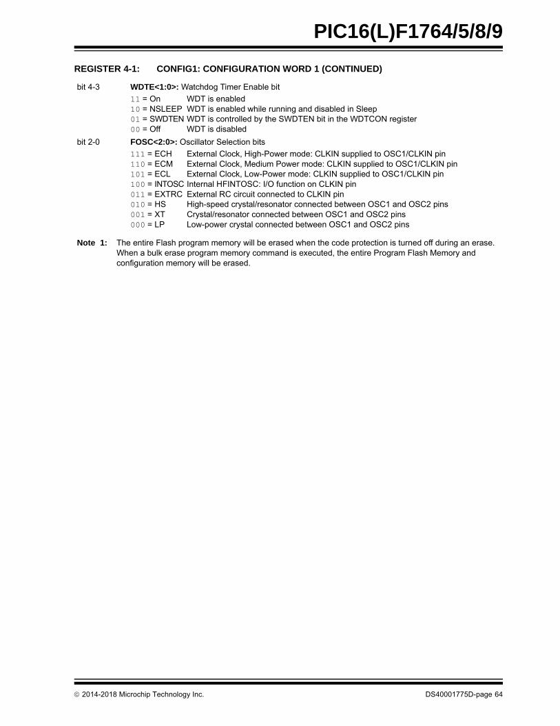
2014-2018 Microchip Technology Inc. DS40001775D-page 64
PIC16(L)F1764/5/8/9
bit 4-3 WDTE<1:0>: Watchdog Timer Enable bit
11 = On WDT is enabled10 = NSLEEP WDT is enabled while running and disabled in Sleep01 = SWDTEN WDT is controlled by the SWDTEN bit in the WDTCON register00 = Off WDT is disabled
bit 2-0 FOSC<2:0>: Oscillator Selection bits
111 = ECH External Clock, High-Power mode: CLKIN supplied to OSC1/CLKIN pin110 = ECM External Clock, Medium Power mode: CLKIN supplied to OSC1/CLKIN pin101 = ECL External Clock, Low-Power mode: CLKIN supplied to OSC1/CLKIN pin100 = INTOSC Internal HFINTOSC: I/O function on CLKIN pin011 = EXTRC External RC circuit connected to CLKIN pin010 = HS High-speed crystal/resonator connected between OSC1 and OSC2 pins001 = XT Crystal/resonator connected between OSC1 and OSC2 pins000 = LP Low-power crystal connected between OSC1 and OSC2 pins
REGISTER 4-1: CONFIG1: CONFIGURATION WORD 1 (CONTINUED)
Note 1: The entire Flash program memory will be erased when the code protection is turned off during an erase. When a bulk erase program memory command is executed, the entire Program Flash Memory and configuration memory will be erased.
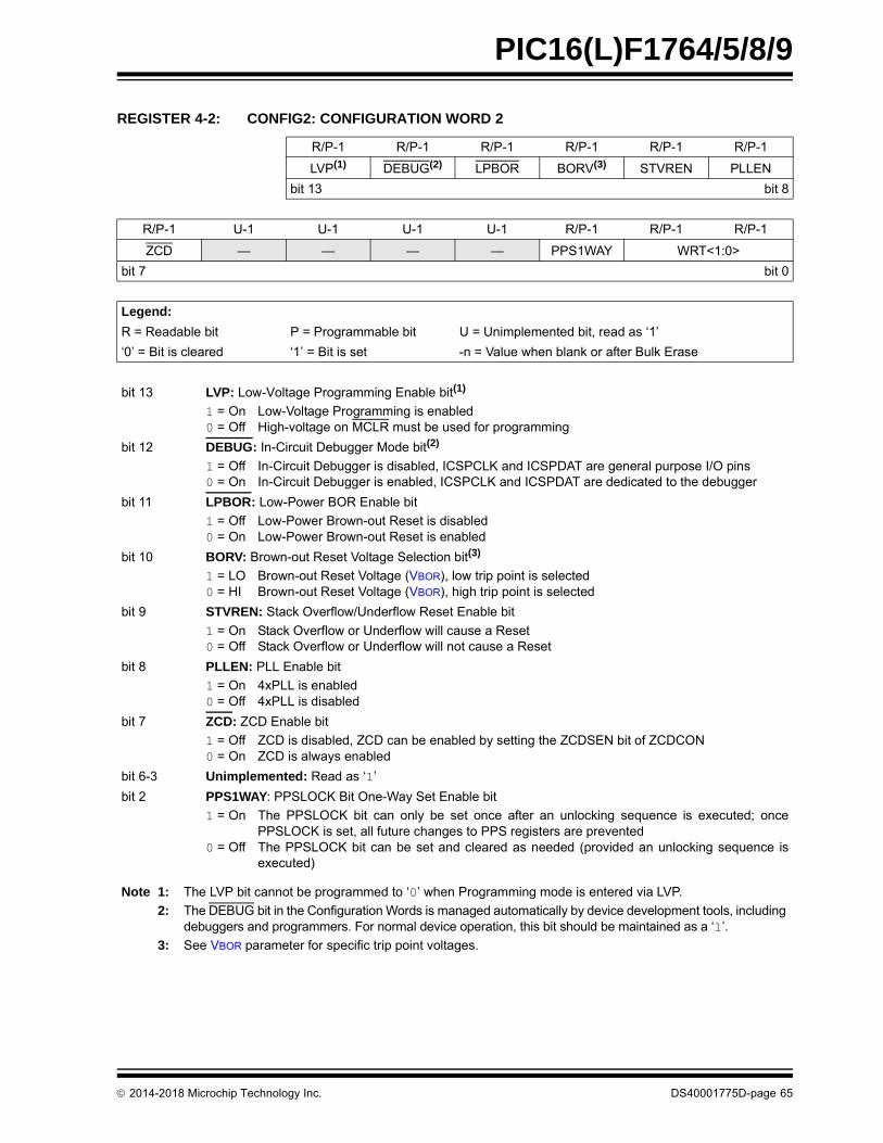
2014-2018 Microchip Technology Inc. DS40001775D-page 65
PIC16(L)F1764/5/8/9
REGISTER 4-2: CONFIG2: CONFIGURATION WORD 2
R/P-1 R/P-1 R/P-1 R/P-1 R/P-1 R/P-1
LVP(1) DEBUG(2) LPBOR BORV(3) STVREN PLLEN
bit 13 bit 8
R/P-1 U-1 U-1 U-1 U-1 R/P-1 R/P-1 R/P-1
ZCD — — — — PPS1WAY WRT<1:0>
bit 7 bit 0
Legend:
R = Readable bit P = Programmable bit U = Unimplemented bit, read as ‘1’
‘0’ = Bit is cleared ‘1’ = Bit is set -n = Value when blank or after Bulk Erase
bit 13 LVP: Low-Voltage Programming Enable bit(1)
1 = On Low-Voltage Programming is enabled0 = Off High-voltage on MCLR must be used for programming
bit 12 DEBUG: In-Circuit Debugger Mode bit(2)
1 = Off In-Circuit Debugger is disabled, ICSPCLK and ICSPDAT are general purpose I/O pins0 = On In-Circuit Debugger is enabled, ICSPCLK and ICSPDAT are dedicated to the debugger
bit 11 LPBOR: Low-Power BOR Enable bit
1 = Off Low-Power Brown-out Reset is disabled0 = On Low-Power Brown-out Reset is enabled
bit 10 BORV: Brown-out Reset Voltage Selection bit(3)
1 = LO Brown-out Reset Voltage (VBOR), low trip point is selected0 = HI Brown-out Reset Voltage (VBOR), high trip point is selected
bit 9 STVREN: Stack Overflow/Underflow Reset Enable bit
1 = On Stack Overflow or Underflow will cause a Reset0 = Off Stack Overflow or Underflow will not cause a Reset
bit 8 PLLEN: PLL Enable bit
1 = On 4xPLL is enabled0 = Off 4xPLL is disabled
bit 7 ZCD: ZCD Enable bit
1 = Off ZCD is disabled, ZCD can be enabled by setting the ZCDSEN bit of ZCDCON0 = On ZCD is always enabled
bit 6-3 Unimplemented: Read as ‘1’
bit 2 PPS1WAY: PPSLOCK Bit One-Way Set Enable bit
1 = On The PPSLOCK bit can only be set once after an unlocking sequence is executed; oncePPSLOCK is set, all future changes to PPS registers are prevented
0 = Off The PPSLOCK bit can be set and cleared as needed (provided an unlocking sequence isexecuted)
Note 1: The LVP bit cannot be programmed to ‘0’ when Programming mode is entered via LVP.
2: The DEBUG bit in the Configuration Words is managed automatically by device development tools, including debuggers and programmers. For normal device operation, this bit should be maintained as a ‘1’.
3: See VBOR parameter for specific trip point voltages.

2014-2018 Microchip Technology Inc. DS40001775D-page 66
PIC16(L)F1764/5/8/9
bit 1-0 WRT<1:0>: Flash Memory Self-Write Protection bits
4 kW Flash Memory (PIC16(L)F1764/8):11 = Off Write protection is off10 = Boot 0000h to 01FFh are write-protected, 0200h to 0FFFh may be modified by PMCON control01 = Half 0000h to 07FFh are write-protected, 0800h to 0FFFh may be modified by PMCON control00 = All 0000h to 0FFFh are write-protected, no addresses may be modified by PMCON control
8 kW Flash Memory (PIC16(L)F1765/9):11 = Off Write protection is off10 = Boot 0000h to 01FFh are write-protected, 0200h to 1FFFh may be modified by PMCON control01 = Half 0000h to 0FFFh are write-protected, 1000h to 1FFFh may be modified by PMCON control00 = All 0000h to 1FFFh are write-protected, no addresses may be modified by PMCON control
REGISTER 4-2: CONFIG2: CONFIGURATION WORD 2 (CONTINUED)
Note 1: The LVP bit cannot be programmed to ‘0’ when Programming mode is entered via LVP.
2: The DEBUG bit in the Configuration Words is managed automatically by device development tools, including debuggers and programmers. For normal device operation, this bit should be maintained as a ‘1’.
3: See VBOR parameter for specific trip point voltages.

2014-2018 Microchip Technology Inc. DS40001775D-page 67
PIC16(L)F1764/5/8/9
4.3 Code Protection
Code protection allows the device to be protected fromunauthorized access. Program memory protection iscontrolled independently. Internal access to theprogram memory is unaffected by any code protectionsetting.
4.3.1 PROGRAM MEMORY PROTECTION
The entire program memory space is protected fromexternal reads and writes by the CP bit in theConfiguration Words. When CP = 0, external reads andwrites of program memory are inhibited and a read willreturn all ‘0’s. The CPU can continue to read programmemory, regardless of the protection bit settings.Writing the program memory is dependent upon thewrite protection setting. See Section 4.4 “WriteProtection” for more information.
4.4 Write Protection
Write protection allows the device to be protected fromunintended self-writes. Applications, such as bootloader software, can be protected while allowing otherregions of the program memory to be modified.
The WRT<1:0> bits in the Configuration Words definethe size of the program memory block that is protected.
4.5 User ID
Four memory locations (8000h-8003h) are designatedas ID locations where the user can store checksum orother code identification numbers. These locations arereadable and writable during normal execution. SeeSection 10.4 “User ID, Device ID and ConfigurationWord Access” for more information on accessingthese memory locations. For more information onchecksum calculation, see the “PIC16(L)F170XMemory Programming Specification” (DS40001683).

2014-2018 Microchip Technology Inc. DS40001775D-page 68
PIC16(L)F1764/5/8/9
4.6 Device ID and Revision ID
The 14-bit Device ID word is located at 8006h and the14-bit Revision ID is located at 8005h. These locationsare read-only and cannot be erased or modified. SeeSection 10.4 “User ID, Device ID and ConfigurationWord Access” for more information on accessingthese memory locations.
Development tools, such as device programmers anddebuggers, may be used to read the Device ID andRevision ID.
4.7 Register Definitions: Device and Revision REGISTER 4-3: DEVID: DEVICE ID REGISTER
R R R R R R
DEV<13:8>
bit 13 bit 8
R R R R R R R R
DEV<7:0>
bit 7 bit 0
Legend:
R = Readable bit ‘1’ = Bit is set ‘0’ = Bit is cleared
bit 13-0 DEV<13:0>: Device ID bits
Device DEVID<13:0> Values
PIC16F1764 11 0000 1000 0000 (3080h)
PIC16F1765 11 0000 1000 0001 (3081h)
PIC16F1768 11 0000 1000 0100 (3084h)
PIC16F1769 11 0000 1000 0101 (3085h)
PIC16LF1764 11 0000 1000 0010 (3082h)
PIC16LF1765 11 0000 1000 0011 (3083h)
PIC16LF1768 11 0000 1000 0110 (3086h)
PIC16LF1769 11 0000 1000 0111 (3087h)
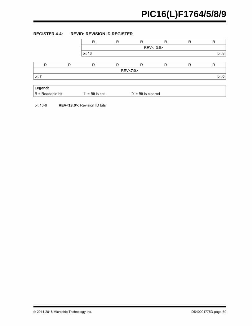
2014-2018 Microchip Technology Inc. DS40001775D-page 69
PIC16(L)F1764/5/8/9
REGISTER 4-4: REVID: REVISION ID REGISTER
R R R R R R
REV<13:8>
bit 13 bit 8
R R R R R R R R
REV<7:0>
bit 7 bit 0
Legend:
R = Readable bit ‘1’ = Bit is set ‘0’ = Bit is cleared
bit 13-0 REV<13:0>: Revision ID bits

2014-2018 Microchip Technology Inc. DS40001775D-page 70
PIC16(L)F1764/5/8/9
5.0 OSCILLATOR MODULE (WITH FAIL-SAFE CLOCK MONITOR)
5.1 Overview
The oscillator module has a wide variety of clocksources and selection features that allow it to be usedin a wide range of applications while maximizing perfor-mance and minimizing power consumption. Figure 5-1illustrates a block diagram of the oscillator module.
Clock sources can be supplied from external oscillators,quartz crystal resonators, ceramic resonators andResistor-Capacitor (RC) circuits. In addition, the systemclock source can be supplied from one of two internaloscillators and PLL circuits, with a choice of speedsselectable via software. Additional clock featuresinclude:
• Selectable system clock source between external or internal sources via software.
• Two-Speed Start-up mode, which minimizes latency between external oscillator start-up and code execution.
• Fail-Safe Clock Monitor (FSCM) designed to detect a failure of the external clock source (LP, XT, HS, ECH, ECM, ECL or EXTRC modes) and switch automatically to the internal oscillator.
• Oscillator Start-up Timer (OST) ensures stability of crystal oscillator sources.
The oscillator module can be configured in one of thefollowing clock modes.
1. ECL – External Clock Low-Power mode(0 MHz to 0.5 MHz).
2. ECM – External Clock Medium Power mode(0.5 MHz to 4 MHz).
3. ECH – External Clock High-Power mode(4 MHz to 32 MHz).
4. LP – 32 kHz Low-Power Crystal mode.
5. XT – Medium Gain Crystal or Ceramic ResonatorOscillator mode (up to 4 MHz).
6. HS – High Gain Crystal or Ceramic Resonatormode (4 MHz to 20 MHz).
7. EXTRC – External Resistor-Capacitor.
8. INTOSC – Internal Oscillator (31 kHz to 32 MHz).
Clock source modes are selected by the FOSC<2:0>bits in the Configuration Words. The FOSCx bitsdetermine the type of oscillator that will be used whenthe device is first powered.
The ECH, ECM and ECL Clock modes rely on anexternal logic level signal as the device clock source.The LP, XT and HS Clock modes require an externalcrystal or resonator to be connected to the device.Each mode is optimized for a different frequency range.The EXTRC Clock mode requires an external resistorand capacitor to set the oscillator frequency.
The Internal Oscillator Block (INTOSC) produces low,medium and high-frequency clock sources, designatedLFINTOSC, MFINTOSC and HFINTOSC (see InternalOscillator Block, Figure 5-1). A wide selection of deviceclock frequencies may be derived from these threeclock sources.

2014-2018 Microchip Technology Inc. DS40001775D-page 71
PIC16(L)F1764/5/8/9
FIGURE 5-1: SIMPLIFIED PIC® MCU CLOCK SOURCE BLOCK DIAGRAM
Secondary
T1OSCENEnableOscillator
SOSCO
SOSCI
Timer1 Clock Source Option for Other Modules
OSC1
OSC2
Sleep
LP, XT, HS, RC, EC
T1OSC
To CPU and
Pos
tsca
ler
MU
X
16 MHz
8 MHz4 MHz2 MHz1 MHz
250 kHz500 kHz
IRCF<3:0>
31 kHz
500 kHzSource
InternalOscillator
Block
WDT, PWRT, Fail-Safe Clock Monitor,
16 MHz
INTOSC
(HFINTOSC)
SCS<1:0>
HFPLL
31 kHz (LFINTOSC)Two-Speed Start-up and Other Modules
Oscillator
31 kHzSource
500 kHz(MFINTOSC)
125 kHz
31.25 kHz62.5 kHz
Peripherals
Sleep
External
Timer1
4 x PLL
1x
01
00
1
00
1
PRIMUX
PLLMUX
0000
1111
Inputs Outputs
SCS<1:0> FOSC<2:0>PLLEN orSPLLEN
IRCF<3:0> PRIMUX PLLMUX
= 00
= 100
0 xxxx 1 0
1= 1110 1 1
≠ 1110 1 0
≠ 1000 xxxx 0 0
1 xxxx 0 1
≠ 00 x x xxxx x x
FOSC
Oscillator

2014-2018 Microchip Technology Inc. DS40001775D-page 72
PIC16(L)F1764/5/8/9
5.2 Clock Source Types
Clock sources can be classified as external or internal.
External clock sources rely on external circuitry for theclock source to function. Examples are: oscillatormodules (ECH, ECM, ECL modes), quartz crystal res-onators or ceramic resonators (LP, XT and HS modes)and Resistor-Capacitor (EXTRC) mode circuits.
Internal clock sources are contained within the oscillatormodule. The Internal Oscillator Block has two internaloscillators and a dedicated Phase-Locked Loop(HFPLL) that are used to generate three internal systemclock sources: the 16 MHz High-Frequency InternalOscillator (HFINTOSC), 500 kHz Medium FrequencyInternal Oscillator (MFINTOSC) and the 31 kHzLow-Frequency Internal Oscillator (LFINTOSC).
The system clock can be selected between external orinternal clock sources via the System Clock Select(SCSx) bits in the OSCCON register. See Section 5.3“Clock Switching” for additional information.
5.2.1 EXTERNAL CLOCK SOURCES
An external clock source can be used as the devicesystem clock by performing one of the followingactions:
• Program the FOSC<2:0> bits in the Configuration Words to select an external clock source that will be used as the default system clock upon a device Reset.
• Write the SCS<1:0> bits in the OSCCON register to switch the system clock source to:
- Secondary oscillator during run time, or
- An external clock source determined by the value of the FOSCx bits.
See Section 5.3 “Clock Switching” for moreinformation.
5.2.1.1 EC Mode
The External Clock (EC) mode allows an externallygenerated logic level signal to be the system clocksource. When operating in this mode, an externalclock source is connected to the OSC1 input.OSC2/CLKOUT is available for general purpose I/O orCLKOUT. Figure 5-2 shows the pin connections for ECmode.
EC mode has three power modes to select from throughthe Configuration Words:
• ECH – High power, 4-32 MHz
• ECM – Medium power, 0.5-4 MHz
• ECL – Low power, 0-0.5 MHz
The Oscillator Start-up Timer (OST) is disabled whenEC mode is selected. Therefore, there is no delay inoperation after a Power-on Reset (POR) or wake-upfrom Sleep. Because the PIC® MCU design is fullystatic, stopping the external clock input will have theeffect of halting the device while leaving all data intact.Upon restarting the external clock, the device willresume operation as if no time had elapsed.
FIGURE 5-2: EXTERNAL CLOCK (EC) MODE OPERATION
5.2.1.2 LP, XT, HS Modes
The LP, XT and HS modes support the use of quartzcrystal resonators or ceramic resonators connected toOSC1 and OSC2 (Figure 5-3). The three modes selecta low, medium or high gain setting of the internalinverter-amplifier to support various resonator typesand speed.
LP Oscillator mode selects the lowest gain setting of theinternal inverter-amplifier. LP mode current consumptionis the least of the three modes. This mode is designed todrive only 32.768 kHz tuning-fork type crystals (watchcrystals).
XT Oscillator mode selects the intermediate gainsetting of the internal inverter-amplifier. XT modecurrent consumption is the medium of the three modes.This mode is best suited to drive resonators with amedium drive level specification.
HS Oscillator mode selects the highest gain setting of theinternal inverter-amplifier. HS mode current consumptionis the highest of the three modes. This mode is bestsuited for resonators that require a high drive setting.
Figure 5-3 and Figure 5-4 show typical circuits forquartz crystal and ceramic resonators, respectively.
Clock fromExt. system
FOSC/4 or I/O(1)
OSC1/CLKIN
PIC® MCU
OSC2/CLKOUT
Note 1: Output depends upon the CLKOUTEN bitof the Configuration Words.
Rev. 10-000045A7/30/2013

2014-2018 Microchip Technology Inc. DS40001775D-page 73
PIC16(L)F1764/5/8/9
FIGURE 5-3: QUARTZ CRYSTAL OPERATION (LP, XT OR HS MODE)
FIGURE 5-4: CERAMIC RESONATOR OPERATION(XT OR HS MODE)
5.2.1.3 Oscillator Start-up Timer (OST)
If the oscillator module is configured for LP, XT or HSmodes, the Oscillator Start-up Timer (OST) counts1024 oscillations from OSC1. This occurs following aPower-on Reset (POR) and when the Power-up Timer(PWRT) has expired (if configured), or a wake-up fromSleep. During this time, the Program Counter does notincrement and program execution is suspended,unless either FSCM or Two-Speed Start-up is enabled.In this case, code will continue to execute at theselected INTOSC frequency while the OST is counting.The OST ensures that the oscillator circuit, using aquartz crystal resonator or ceramic resonator, hasstarted and is providing a stable system clock to theoscillator module.
In order to minimize latency between external oscillatorstart-up and code execution, the Two-Speed ClockStart-up mode can be selected (see Section 5.4“Two-Speed Clock Start-up Mode”).
Note 1: Quartz crystal characteristics vary accord-ing to type, package and manufacturer.The user should consult the manufacturerdata sheets for specifications andrecommended application.
2: Always verify oscillator performance overthe VDD and temperature range that isexpected for the application.
3: For oscillator design assistance, referencethe following Microchip Application Notes:
• AN826, “Crystal Oscillator Basics and Crystal Selection for rfPIC® and PIC® Devices” (DS00826)
• AN849, “Basic PIC® Oscillator Design” (DS00849)
• AN943, “Practical PIC® Oscillator Analysis and Design” (DS00943)
• AN949, “Making Your Oscillator Work” (DS00949)
RS(1)
OSC1/CLKIN
PIC® MCU
OSC2/CLKOUT
Note 1: A series resistor (Rs) may be required forquartz crystals with low drive level.
2: The value of RF varies with the Oscillator modeselected (typically between 2 MΩ and 10 MΩ).
RF(2)
C2
C1 To InternalLogic
SleepQuartzCrystal
Rev. 10-000059A7/30/2013
RS(1)
OSC1/CLKIN
PIC® MCU
OSC2/CLKOUT
Note 1: A series resistor (Rs) may be required forceramic resonators with low drive level.
2: The value of RF varies with the Oscillator modeselected (typically between 2 MΩ and 10 MΩ).
3. An additional parallel feedback resistor (RP)may be required for proper ceramic resonatoroperation.
RF(2)
C2
C1 To InternalLogic
SleepRP(3)
CeramicResonator
Rev. 10-000060A7/30/2013
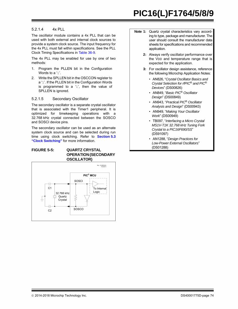
2014-2018 Microchip Technology Inc. DS40001775D-page 74
PIC16(L)F1764/5/8/9
5.2.1.4 4x PLL
The oscillator module contains a 4x PLL that can beused with both external and internal clock sources toprovide a system clock source. The input frequency forthe 4x PLL must fall within specifications. See the PLLClock Timing Specifications in Table 36-9.
The 4x PLL may be enabled for use by one of twomethods:
1. Program the PLLEN bit in the ConfigurationWords to a ‘1’.
2. Write the SPLLEN bit in the OSCCON register toa ‘1’. If the PLLEN bit in the Configuration Wordsis programmed to a ‘1’, then the value ofSPLLEN is ignored.
5.2.1.5 Secondary Oscillator
The secondary oscillator is a separate crystal oscillatorthat is associated with the Timer1 peripheral. It isoptimized for timekeeping operations with a32.768 kHz crystal connected between the SOSCOand SOSCI device pins.
The secondary oscillator can be used as an alternatesystem clock source and can be selected during runtime using clock switching. Refer to Section 5.3“Clock Switching” for more information.
FIGURE 5-5: QUARTZ CRYSTAL OPERATION (SECONDARY OSCILLATOR)
SOSCI
PIC® MCU
SOSCOC2
C1 To InternalLogic32.768 kHz
QuartzCrystal
Rev. 10-000061A7/30/2013
Note 1: Quartz crystal characteristics vary accord-ing to type, package and manufacturer. Theuser should consult the manufacturer datasheets for specifications and recommendedapplication.
2: Always verify oscillator performance overthe VDD and temperature range that isexpected for the application.
3: For oscillator design assistance, referencethe following Microchip Application Notes:
• AN826, “Crystal Oscillator Basics and Crystal Selection for rfPIC® and PIC® Devices” (DS00826)
• AN849, “Basic PIC® Oscillator Design” (DS00849)
• AN943, “Practical PIC® Oscillator Analysis and Design” (DS00943)
• AN949, “Making Your Oscillator Work” (DS00949)
• TB097, “Interfacing a Micro Crystal MS1V-T1K 32.768 kHz Tuning Fork Crystal to a PIC16F690/SS” (DS91097)
• AN1288, “Design Practices for Low-Power External Oscillators” (DS01288)

2014-2018 Microchip Technology Inc. DS40001775D-page 75
PIC16(L)F1764/5/8/9
5.2.1.6 External RC Mode
The external Resistor-Capacitor (EXTRC) mode sup-ports the use of an external RC circuit. This allows thedesigner maximum flexibility in frequency choice whilekeeping costs to a minimum when clock accuracy is notrequired.
The RC circuit connects to OSC1. OSC2/CLKOUT isavailable for general purpose I/O or CLKOUT. Thefunction of the OSC2/CLKOUT pin is determined by theCLKOUTEN bit in the Configuration Words.
Figure 5-6 shows the external RC mode connections.
FIGURE 5-6: EXTERNAL RC MODES
The RC oscillator frequency is a function of the supplyvoltage, the Resistor (REXT) and Capacitor (CEXT)values, and the operating temperature. Other factorsaffecting the oscillator frequency are:
• Threshold voltage variation• Component tolerances• Packaging variations in capacitance
The user also needs to take into account variation dueto tolerance of external RC components used.
5.2.2 INTERNAL CLOCK SOURCES
The device may be configured to use the Internal Oscil-lator Block as the system clock by performing one ofthe following actions:
• Program the FOSC<2:0> bits in the Configuration Words to select the INTOSC clock source, which will be used as the default system clock upon a device Reset.
• Write the SCS<1:0> bits in the OSCCON register to switch the system clock source to the internal oscillator during run time. See Section 5.3 “Clock Switching” for more information.
In INTOSC mode, OSC1/CLKIN is available for generalpurpose I/O. OSC2/CLKOUT is available for generalpurpose I/O or CLKOUT.
The function of the OSC2/CLKOUT pin is determinedby the CLKOUTEN bit in the Configuration Words.
The Internal Oscillator Block has two independentoscillators and a dedicated Phase-Locked Loop(HFPLL) that can produce one of three internal systemclock sources.
1. The HFINTOSC (High-Frequency InternalOscillator) is factory calibrated and operates at16 MHz. The HFINTOSC source is generatedfrom the 500 kHz MFINTOSC source and thededicated Phase-Locked Loop, HFPLL. Thefrequency of the HFINTOSC can beuser-adjusted via software using the OSCTUNEregister (Register 5-3).
2. The MFINTOSC (Medium Frequency InternalOscillator) is factory calibrated and operates at500 kHz. The frequency of the MFINTOSC canbe user-adjusted via software using theOSCTUNE register (Register 5-3).
3. The LFINTOSC (Low-Frequency InternalOscillator) is uncalibrated and operates at31 kHz.
FOSC/4 or I/O(1)
PIC® MCU
OSC2/CLKOUT
Note 1: Output depends upon the CLKOUTEN bit of the Configuration Words.
OSC1/CLKIN Internal Clock
VSS
CEXT
REXT
Recommended values:10 k REXT 100 k , <3V3 k REXT 100 k , 3-5VCEXT > 20 pF, 2-5V
Rev. 10-000062A7/31/2013
VDD

2014-2018 Microchip Technology Inc. DS40001775D-page 76
PIC16(L)F1764/5/8/9
5.2.2.1 HFINTOSC
The High-Frequency Internal Oscillator (HFINTOSC) isa factory calibrated, 16 MHz internal clock source. Thefrequency of the HFINTOSC can be altered viasoftware using the OSCTUNE register (Register 5-3).
The output of the HFINTOSC connects to a postscalerand multiplexer (see Figure 5-1). One of multiplefrequencies derived from the HFINTOSC can beselected via software using the IRCF<3:0> bits of theOSCCON register. See Section 5.2.2.7 “InternalOscillator Clock Switch Timing” for more information.
The HFINTOSC is enabled by:
• Configuring the IRCF<3:0> bits of the OSCCON register for the desired HF frequency, and
• FOSC<2:0> = 100, or
• Setting the System Clock Source (SCS<1:0>) bits of the OSCCON register to ‘1x’
A fast start-up oscillator allows internal circuits to powerup and stabilize before switching to HFINTOSC.
The High-Frequency Internal Oscillator Ready bit(HFIOFR) of the OSCSTAT register indicates when theHFINTOSC is running.
The High-Frequency Internal Oscillator Status Lockedbit (HFIOFL) of the OSCSTAT register indicates whenthe HFINTOSC is running within 2% of its final value.
The High-Frequency Internal Oscillator Stable bit(HFIOFS) of the OSCSTAT register indicates when theHFINTOSC is running within 0.5% of its final value.
5.2.2.2 MFINTOSC
The Medium Frequency Internal Oscillator (MFINTOSC)is a factory calibrated 500 kHz internal clock source.The frequency of the MFINTOSC can be altered viasoftware using the OSCTUNE register (Register 5-3).
The output of the MFINTOSC connects to a postscalerand multiplexer (see Figure 5-1). One of ninefrequencies derived from the MFINTOSC can beselected via software using the IRCF<3:0> bits of theOSCCON register. See Section 5.2.2.7 “InternalOscillator Clock Switch Timing” for more information.
The MFINTOSC is enabled by:
• Configuring the IRCF<3:0> bits of the OSCCON register for the desired HF frequency, and
• FOSC<2:0> = 100, or
• Setting the System Clock Source (SCS<1:0>) bits of the OSCCON register to ‘1x’
The Medium Frequency Internal Oscillator Ready bit(MFIOFR) of the OSCSTAT register indicates when theMFINTOSC is running.
5.2.2.3 Internal Oscillator Frequency Adjustment
The 500 kHz internal oscillator is factory calibrated.This internal oscillator can be adjusted in software bywriting to the OSCTUNE register (Register 5-3). Sincethe HFINTOSC and MFINTOSC clock sources arederived from the 500 kHz internal oscillator, a changein the OSCTUNE register value will apply to both.
The default value of the OSCTUNE register is ‘0’. Thevalue is a 6-bit two’s complement number. A value of1Fh will provide an adjustment to the maximumfrequency. A value of 20h will provide an adjustment tothe minimum frequency.
When the OSCTUNE register is modified, the oscillatorfrequency will begin shifting to the new frequency. Codeexecution continues during this shift. There is noindication that the shift has occurred.
OSCTUNE does not affect the LFINTOSC frequency.Operation of features that depend on the LFINTOSCclock source frequency, such as the Power-up Timer(PWRT), Watchdog Timer (WDT), Fail-Safe ClockMonitor (FSCM) and peripherals, are not affected by thechange in frequency.
5.2.2.4 LFINTOSC
The Low-Frequency Internal Oscillator (LFINTOSC) isan uncalibrated 31 kHz internal clock source.
The output of the LFINTOSC connects to a multiplexer(see Figure 5-1). Select 31 kHz, via software, using theIRCF<3:0> bits of the OSCCON register. SeeSection 5.2.2.7 “Internal Oscillator Clock SwitchTiming” for more information. The LFINTOSC is alsothe frequency for the Power-up Timer (PWRT),Watchdog Timer (WDT) and Fail-Safe Clock Monitor(FSCM).
The LFINTOSC is enabled by selecting 31 kHz(IRCF<3:0> (OSCCON<6:3>) = 000) as the systemclock source (SCS<1:0> (OSCCON<1:0> = 1x) orwhen any of the following are enabled:
• Configuring the IRCF<3:0> bits of the OSCCON register for the desired LF frequency, and
• FOSC<2:0> = 100, or
• Setting the System Clock Source (SCS<1:0>) bits of the OSCCON register to ‘1x’
Peripherals that use the LFINTOSC are:
• Power-up Timer (PWRT)
• Watchdog Timer (WDT)
• Fail-Safe Clock Monitor (FSCM)
The Low-Frequency Internal Oscillator Ready bit(LFIOFR) of the OSCSTAT register indicates when theLFINTOSC is running.
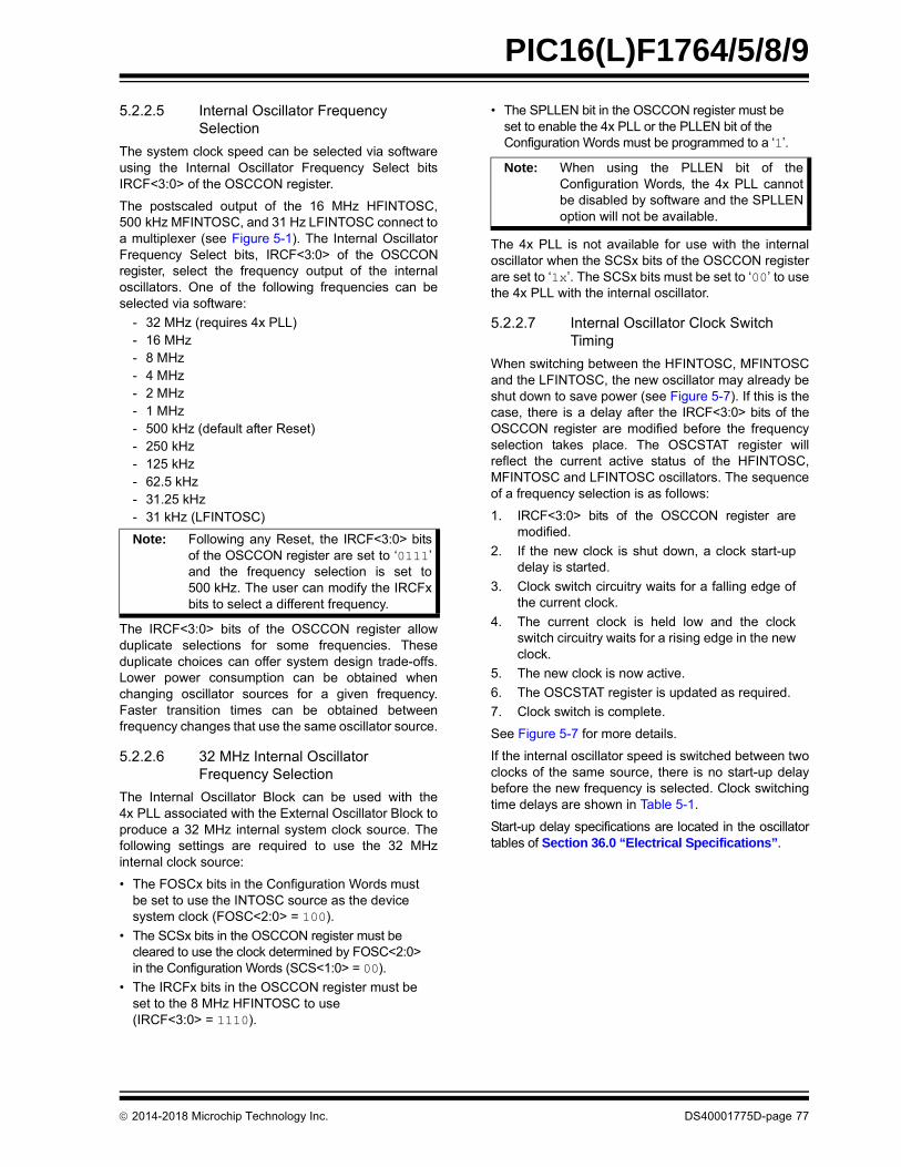
2014-2018 Microchip Technology Inc. DS40001775D-page 77
PIC16(L)F1764/5/8/9
5.2.2.5 Internal Oscillator Frequency Selection
The system clock speed can be selected via softwareusing the Internal Oscillator Frequency Select bitsIRCF<3:0> of the OSCCON register.
The postscaled output of the 16 MHz HFINTOSC,500 kHz MFINTOSC, and 31 Hz LFINTOSC connect toa multiplexer (see Figure 5-1). The Internal OscillatorFrequency Select bits, IRCF<3:0> of the OSCCONregister, select the frequency output of the internaloscillators. One of the following frequencies can beselected via software:
- 32 MHz (requires 4x PLL)- 16 MHz- 8 MHz- 4 MHz- 2 MHz- 1 MHz- 500 kHz (default after Reset)- 250 kHz- 125 kHz- 62.5 kHz- 31.25 kHz- 31 kHz (LFINTOSC)
The IRCF<3:0> bits of the OSCCON register allowduplicate selections for some frequencies. Theseduplicate choices can offer system design trade-offs.Lower power consumption can be obtained whenchanging oscillator sources for a given frequency.Faster transition times can be obtained betweenfrequency changes that use the same oscillator source.
5.2.2.6 32 MHz Internal Oscillator Frequency Selection
The Internal Oscillator Block can be used with the4x PLL associated with the External Oscillator Block toproduce a 32 MHz internal system clock source. Thefollowing settings are required to use the 32 MHzinternal clock source:
• The FOSCx bits in the Configuration Words must be set to use the INTOSC source as the device system clock (FOSC<2:0> = 100).
• The SCSx bits in the OSCCON register must be cleared to use the clock determined by FOSC<2:0> in the Configuration Words (SCS<1:0> = 00).
• The IRCFx bits in the OSCCON register must be set to the 8 MHz HFINTOSC to use (IRCF<3:0> = 1110).
• The SPLLEN bit in the OSCCON register must be set to enable the 4x PLL or the PLLEN bit of the Configuration Words must be programmed to a ‘1’.
The 4x PLL is not available for use with the internaloscillator when the SCSx bits of the OSCCON registerare set to ‘1x’. The SCSx bits must be set to ‘00’ to usethe 4x PLL with the internal oscillator.
5.2.2.7 Internal Oscillator Clock Switch Timing
When switching between the HFINTOSC, MFINTOSCand the LFINTOSC, the new oscillator may already beshut down to save power (see Figure 5-7). If this is thecase, there is a delay after the IRCF<3:0> bits of theOSCCON register are modified before the frequencyselection takes place. The OSCSTAT register willreflect the current active status of the HFINTOSC,MFINTOSC and LFINTOSC oscillators. The sequenceof a frequency selection is as follows:
1. IRCF<3:0> bits of the OSCCON register aremodified.
2. If the new clock is shut down, a clock start-updelay is started.
3. Clock switch circuitry waits for a falling edge ofthe current clock.
4. The current clock is held low and the clockswitch circuitry waits for a rising edge in the newclock.
5. The new clock is now active.
6. The OSCSTAT register is updated as required.
7. Clock switch is complete.
See Figure 5-7 for more details.
If the internal oscillator speed is switched between twoclocks of the same source, there is no start-up delaybefore the new frequency is selected. Clock switchingtime delays are shown in Table 5-1.
Start-up delay specifications are located in the oscillatortables of Section 36.0 “Electrical Specifications”.
Note: Following any Reset, the IRCF<3:0> bitsof the OSCCON register are set to ‘0111’and the frequency selection is set to500 kHz. The user can modify the IRCFxbits to select a different frequency.
Note: When using the PLLEN bit of theConfiguration Words, the 4x PLL cannotbe disabled by software and the SPLLENoption will not be available.

2014-2018 Microchip Technology Inc. DS40001775D-page 78
PIC16(L)F1764/5/8/9
FIGURE 5-7: INTERNAL OSCILLATOR SWITCH TIMING
HFINTOSC/
LFINTOSC
IRCF<3:0>
System Clock
HFINTOSC/
LFINTOSC
IRCF<3:0>
System Clock
0 0
0 0
Start-up Time 2-Cycle Sync Running
2-Cycle Sync Running
HFINTOSC/ LFINTOSC (FSCM and WDT disabled)
HFINTOSC/ LFINTOSC (Either FSCM or WDT enabled)
LFINTOSC
HFINTOSC/
IRCF <3:0>
System Clock
0 0
Start-up Time 2-Cycle Sync Running
LFINTOSC HFINTOSC/MFINTOSCLFINTOSC Turns Off unless WDT or FSCM is Enabled
MFINTOSC
MFINTOSC
MFINTOSC
MFINTOSC
MFINTOSC

2014-2018 Microchip Technology Inc. DS40001775D-page 79
PIC16(L)F1764/5/8/9
5.3 Clock Switching
The system clock source can be switched betweenexternal and internal clock sources via software usingthe System Clock Select (SCS) bits of the OSCCONregister. The following clock sources can be selectedusing the SCS<1:0> bits:
• Default system oscillator determined by the FOSCx bits in the Configuration Words
• Timer1 32 kHz crystal oscillator
• Internal Oscillator Block (INTOSC)
5.3.1 SYSTEM CLOCK SELECT (SCS) BITS
The System Clock Select (SCS<1:0>) bits of theOSCCON register select the system clock source thatis used for the CPU and peripherals.
• When SCS<1:0> = 00, the system clock source is determined by the value of the FOSC<2:0> bits in the Configuration Words.
• When SCS<1:0> = 01, the system clock source is the secondary oscillator.
• When SCS<1:0> = 1x, the system clock source is chosen by the internal oscillator frequency selected by the IRCF<3:0> bits of the OSCCON register. After a Reset, the SCSx bits of the OSCCON register are always cleared.
When switching between clock sources, a delay isrequired to allow the new clock to stabilize. Theseoscillator delays are shown in Table 5-1.
5.3.2 OSCILLATOR START-UP TIMER STATUS (OSTS) BIT
The Oscillator Start-up Timer Status (OSTS) bit of theOSCSTAT register indicates whether the system clockis running from the external clock source, as defined bythe FOSC<2:0> bits in the Configuration Words, orfrom the internal clock source. In particular, OSTSindicates that the Oscillator Start-up Timer (OST) hastimed out for LP, XT or HS modes. The OST does notreflect the status of the secondary oscillator.
5.3.3 SECONDARY OSCILLATOR
The secondary oscillator is a separate crystal oscillatorassociated with the Timer1 peripheral. It is optimizedfor timekeeping operations with a 32.768 kHz crystalconnected between the SOSCO and SOSCI devicepins.
The secondary oscillator is enabled using the OSCENcontrol bit in the T1CON register. See Section 22.0“Timer1/3/5 Module with Gate Control” for moreinformation about the Timer1 peripheral.
5.3.4 SECONDARY OSCILLATOR READY (SOSCR) BIT
The user must ensure that the secondary oscillator isready to be used before it is selected as a system clocksource. The Secondary Oscillator Ready (SOSCR) bitof the OSCSTAT register indicates whether thesecondary oscillator is ready to be used. After theSOSCR bit is set, the SCSx bits can be configured toselect the secondary oscillator.
5.3.5 CLOCK SWITCH BEFORE SLEEP
When a clock switch from an old clock to a new clock isrequested just prior to entering Sleep mode, it isnecessary to confirm that the switch is complete beforethe sleep instruction is executed. Failure to do so mayresult in an incomplete switch and consequential lossof the system clock altogether. Clock switching isconfirmed by monitoring the clock status bits in theOSCSTAT register. Switch confirmation can beaccomplished by sensing that the ready bit for the newclock is set or the ready bit for the old clock is cleared.For example, when switching between the internaloscillator with the PLL and the internal oscillator withoutthe PLL, monitor the PLLR bit. When PLLR is set, theswitch to 32 MHz operation is complete. Conversely,when PLLR is cleared, the switch from 32 MHzoperation to the selected internal clock is complete.
Note: Any automatic clock switch, which mayoccur from Two-Speed Start-up orFail-Safe Clock Monitor, does not updatethe SCS bits of the OSCCON register. Theuser can monitor the OSTS bit of theOSCSTAT register to determine the currentsystem clock source.

2014-2018 Microchip Technology Inc. DS40001775D-page 80
PIC16(L)F1764/5/8/9
5.4 Two-Speed Clock Start-up Mode
Two-Speed Clock Start-up mode provides additionalpower savings by minimizing the latency betweenexternal oscillator start-up and code execution. Inapplications that make heavy use of the Sleep mode,Two-Speed Start-up will remove the external oscillatorstart-up time from the time spent awake and canreduce the overall power consumption of the device.This mode allows the application to wake-up fromSleep, perform a few instructions using the InternalOscillator Block, INTOSC, as the clock source and goback to Sleep without waiting for the external oscillatorto become stable.
Two-Speed Start-up provides benefits when the oscil-lator module is configured for LP, XT or HS modes.The Oscillator Start-up Timer (OST) is enabled forthese modes and must count 1024 oscillations beforethe oscillator can be used as the system clock source.
If the oscillator module is configured for any modeother than LP, XT or HS mode, then Two-SpeedStart-up is disabled. This is because the external clockoscillator does not require any stabilization time afterPOR or an exit from Sleep.
If the OST count reaches 1024 before the deviceenters Sleep mode, the OSTS bit of the OSCSTATregister is set and program execution switches to theexternal oscillator. However, the system may neveroperate from the external oscillator if the time spentawake is very short.
5.4.1 TWO-SPEED START-UP MODE CONFIGURATION
Two-Speed Start-up mode is configured by thefollowing settings:
• IESO (of the Configuration Words) = 1; Internal/External Switchover bit (Two-Speed Start-up mode enabled).
• SCS<1:0> (of the OSCCON register) = 00.• FOSC<2:0> bits in the Configuration Words
configured for LP, XT or HS mode.
Two-Speed Start-up mode is entered after:
• Power-on Reset (POR) and, if enabled, after Power-up Timer (PWRT) has expired, or
• Wake-up from Sleep.
TABLE 5-1: OSCILLATOR SWITCHING DELAYS
Note: Executing a SLEEP instruction will abortthe oscillator start-up time and will causethe OSTS bit of the OSCSTAT register toremain clear.
Switch From Switch To Frequency Oscillator Delay
SleepLFINTOSCMFINTOSCHFINTOSC(1)
31 kHz31.25 kHz-500 kHz31.25 kHz-16 MHz
Oscillator Warm-up Delay (TWARM)(2)
Sleep EC, RC(1) DC- 32 MHz 2 cycles
LFINTOSC EC, RC(1) DC-32 MHz 1 Cycle of Each
SleepSecondary OscillatorLP, XT, HS(1) 32 kHz-20 MHz 1024 Clock Cycles (OST)
Any Clock SourceMFINTOSCHFINTOSC(1)
31.25 kHz-500 kHz31.25 kHz-16 MHz
2 s (approx.)
Any Clock Source LFINTOSC 31 kHz 1 Cycle of Each
Any Clock Source Secondary Oscillator 32 kHz 1024 Clock Cycles (OST)
PLL Inactive PLL Active 16-32 MHz 2 ms (approx.)
Note 1: PLL is inactive.
2: See Table 36-8.

2014-2018 Microchip Technology Inc. DS40001775D-page 81
PIC16(L)F1764/5/8/9
5.4.2 TWO-SPEED START-UP SEQUENCE
1. Wake-up from Power-on Reset or Sleep.
2. Instructions begin execution by the internaloscillator at the frequency set in the IRCF<3:0>bits of the OSCCON register.
3. OST enabled to count 1024 clock cycles.
4. OST timed out, wait for falling edge of theinternal oscillator.
5. OSTS is set.
6. System clock held low until the next falling edgeof new clock (LP, XT or HS mode).
7. System clock is switched to external clocksource.
5.4.3 CHECKING TWO-SPEED CLOCK STATUS
Checking the state of the OSTS bit of the OSCSTATregister will confirm if the microcontroller is runningfrom the external clock source, as defined by theFOSC<2:0> bits in the Configuration Words, or theinternal oscillator.
FIGURE 5-8: TWO-SPEED START-UP
0 1 1022 1023
PC + 1
TOST
INTOSC
OSC1
OSC2
Program Counter
System Clock
PC – N PC

2014-2018 Microchip Technology Inc. DS40001775D-page 82
PIC16(L)F1764/5/8/9
5.5 Fail-Safe Clock Monitor
The Fail-Safe Clock Monitor (FSCM) allows the deviceto continue operating should the external oscillator fail.The FSCM can detect oscillator failure any time afterthe Oscillator Start-up Timer (OST) has expired. TheFSCM is enabled by setting the FCMEN bit in theConfiguration Words. The FSCM is applicable to allexternal Oscillator modes (LP, XT, HS, EC, SecondaryOscillator and RC).
FIGURE 5-9: FSCM BLOCK DIAGRAM
5.5.1 FAIL-SAFE DETECTION
The FSCM module detects a failed oscillator bycomparing the external oscillator to the FSCM sampleclock. The sample clock is generated by dividing theLFINTOSC by 64. See Figure 5-9. Inside the faildetector block is a latch. The external clock sets thelatch on each falling edge of the external clock. Thesample clock clears the latch on each rising edge of thesample clock. A failure is detected when an entirehalf-cycle of the sample clock elapses before theexternal clock goes low.
5.5.2 FAIL-SAFE OPERATION
When the external clock fails, the FSCM switches thedevice clock to an internal clock source and sets the bitflag OSFIF of the PIR2 register. Setting this flag willgenerate an interrupt if the OSFIE bit of the PIE2register is also set. The device firmware can then takesteps to mitigate the problems that may arise from afailed clock. The system clock will continue to besourced from the internal clock source until the devicefirmware successfully restarts the external oscillatorand switches back to external operation.
The internal clock source chosen by the FSCM isdetermined by the IRCF<3:0> bits of the OSCCONregister. This allows the internal oscillator to beconfigured before a failure occurs.
5.5.3 FAIL-SAFE CONDITION CLEARING
The Fail-Safe condition is cleared after a Reset,executing a SLEEP instruction or changing the SCSxbits of the OSCCON register. When the SCSx bits arechanged, the OST is restarted. While the OST isrunning, the device continues to operate from theINTOSC selected in OSCCON. When the OST timesout, the Fail-Safe condition is cleared after successfullyswitching to the external clock source. The OSFIF bitshould be cleared prior to switching to the externalclock source. If the Fail-Safe condition still exists, theOSFIF flag will again become set by hardware.
5.5.4 RESET OR WAKE-UP FROM SLEEP
The FSCM is designed to detect an oscillator failureafter the Oscillator Start-up Timer (OST) has expired.The OST is used after waking up from Sleep and afterany type of Reset. The OST is not used with the EC orRC Clock modes so that the FSCM will be active assoon as the Reset or wake-up has completed. Whenthe FSCM is enabled, the Two-Speed Start-up is alsoenabled. Therefore, the device will always be executingcode while the OST is operating.
External
LFINTOSC÷ 64
S
R
Q
31 kHz(~32 s)
488 Hz(~2 ms)
Clock MonitorLatch
ClockFailure
Detected
Oscillator
Clock
Q
Sample Clock
Note: Due to the wide range of oscillator start-uptimes, the Fail-Safe circuit is not activeduring oscillator start-up (i.e., after exitingReset or Sleep). After an appropriateamount of time, the user should check thestatus bits in the OSCSTAT register toverify the oscillator start-up and that thesystem clock switchover has successfullycompleted.

2014-2018 Microchip Technology Inc. DS40001775D-page 83
PIC16(L)F1764/5/8/9
FIGURE 5-10: FSCM TIMING DIAGRAM
OSCFIF
SystemClock
Output
Sample Clock
FailureDetected
OscillatorFailure
Note: The system clock is normally at a much higher frequency than the sample clock. The relative frequencies inthis example have been chosen for clarity.
(Q)
Test Test Test
Clock Monitor Output

2014-2018 Microchip Technology Inc. DS40001775D-page 84
PIC16(L)F1764/5/8/9
5.6 Register Definitions: Oscillator Control
REGISTER 5-1: OSCCON: OSCILLATOR CONTROL REGISTER
R/W-0/0 R/W-0/0 R/W-1/1 R/W-1/1 R/W-1/1 U-0 R/W-0/0 R/W-0/0
SPLLEN IRCF<3:0> — SCS<1:0>
bit 7 bit 0
Legend:
R = Readable bit W = Writable bit
u = Bit is unchanged x = Bit is unknown U = Unimplemented bit, read as ‘0’
‘1’ = Bit is set ‘0’ = Bit is cleared -n/n = Value at POR and BOR/Value at all other Resets
bit 7 SPLLEN: Software PLL Enable bit
If PLLEN in Configuration Words = 1:SPLLEN bit is ignored; 4x PLL is always enabled (subject to oscillator requirements).
If PLLEN in Configuration Words = 0:1 = 4x PLL Is enabled0 = 4x PLL is disabled
bit 6-3 IRCF<3:0>: Internal Oscillator Frequency Select bits
1111 = 16 MHz HF1110 = 8 MHz or 32 MHz HF(2)
1101 = 4 MHz HF1100 = 2 MHz HF1011 = 1 MHz HF1010 = 500 kHz HF(1)
1001 = 250 kHz HF(1)
1000 = 125 kHz HF(1)
0111 = 500 kHz MF (default upon Reset)0110 = 250 kHz MF0101 = 125 kHz MF0100 = 62.5 kHz MF0011 = 31.25 kHz HF(1)
0010 = 31.25 kHz MF000x = 31 kHz LF
bit 2 Unimplemented: Read as ‘0’
bit 1-0 SCS<1:0>: System Clock Select bits
1x = Internal Oscillator Block01 = Secondary oscillator00 = Clock determined by FOSC<2:0> in the Configuration Words
Note 1: Duplicate frequency derived from HFINTOSC.
2: 32 MHz when SPLLEN bit is set. Refer to Section 5.2.2.6 “32 MHz Internal Oscillator Frequency Selection”.

2014-2018 Microchip Technology Inc. DS40001775D-page 85
PIC16(L)F1764/5/8/9
REGISTER 5-2: OSCSTAT: OSCILLATOR STATUS REGISTER
R-1/q R-0/q R-q/q R-0/q R-0/q R-q/q R-0/0 R-0/q
SOSCR PLLR OSTS HFIOFR HFIOFL MFIOFR LFIOFR HFIOFS
bit 7 bit 0
Legend:
R = Readable bit W = Writable bit q = Conditional
u = Bit is unchanged x = Bit is unknown U = Unimplemented bit, read as ‘0’
‘1’ = Bit is set ‘0’ = Bit is cleared -n/n = Value at POR and BOR/Value at all other Resets
bit 7 SOSCR: Secondary Oscillator Ready bit
If T1OSCEN = 1:1 = Secondary oscillator is ready0 = Secondary oscillator is not ready
If T1OSCEN = 0:1 = Secondary clock source is always ready
bit 6 PLLR 4x PLL Ready bit
1 = 4x PLL is ready0 = 4x PLL is not ready
bit 5 OSTS: Oscillator Start-up Timer Status bit
1 = Running from the clock defined by the FOSC<2:0> bits of the Configuration Words0 = Running from an internal oscillator (FOSC<2:0> = 100)
bit 4 HFIOFR: High-Frequency Internal Oscillator Ready bit
1 = HFINTOSC is ready0 = HFINTOSC is not ready
bit 3 HFIOFL: High-Frequency Internal Oscillator Locked bit
1 = HFINTOSC is at least 2% accurate0 = HFINTOSC is not 2% accurate
bit 2 MFIOFR: Medium Frequency Internal Oscillator Ready bit
1 = MFINTOSC is ready 0 = MFINTOSC is not ready
bit 1 LFIOFR: Low-Frequency Internal Oscillator Ready bit
1 = LFINTOSC is ready0 = LFINTOSC is not ready
bit 0 HFIOFS: High-Frequency Internal Oscillator Stable bit
1 = HFINTOSC is at least 0.5% accurate0 = HFINTOSC is not 0.5% accurate

2014-2018 Microchip Technology Inc. DS40001775D-page 86
PIC16(L)F1764/5/8/9
TABLE 5-2: SUMMARY OF REGISTERS ASSOCIATED WITH CLOCK SOURCES
TABLE 5-3: SUMMARY OF CONFIGURATION WORD WITH CLOCK SOURCES
REGISTER 5-3: OSCTUNE: OSCILLATOR TUNING REGISTER
U-0 U-0 R/W-0/0 R/W-0/0 R/W-0/0 R/W-0/0 R/W-0/0 R/W-0/0
— — TUN<5:0>
bit 7 bit 0
Legend:
R = Readable bit W = Writable bit
u = Bit is unchanged x = Bit is unknown U = Unimplemented bit, read as ‘0’
‘1’ = Bit is set ‘0’ = Bit is cleared -n/n = Value at POR and BOR/Value at all other Resets
bit 7-6 Unimplemented: Read as ‘0’
bit 5-0 TUN<5:0>: Frequency Tuning bits
100000 = Minimum frequency•••111111 = 000000 = Oscillator module is running at the factory-calibrated frequency000001 = •••011110 = 011111 = Maximum frequency
Name Bit 7 Bit 6 Bit 5 Bit 4 Bit 3 Bit 2 Bit 1 Bit 0Register on Page
OSCCON SPLLEN IRCF<3:0> — SCS<1:0> 84
OSCSTAT SOSCR PLLR OSTS HFIOFR HFIOFL MFIOFR LFIOFR HFIOFS 85
OSCTUNE — — TUN<5:0> 86
PIR2 OSFIF C2IF C1IF — BCL1IF C4IF(1) C3IF(1) CCP2IF(1) 106
PIE2 OSFIE C2IE C1IE — BCL1IE C4IE(1) C3IE(1) CCP2IE(1) 103
T1CON CS<1:0> CKPS<1:0> OSCEN SYNC — ON 223
Legend: — = unimplemented location, read as ‘0’. Shaded cells are not used by clock sources.Note 1: PIC16(L)F1768/9 only.
Name Bits Bit -/7 Bit -/6 Bit 13/5 Bit 12/4 Bit 11/3 Bit 10/2 Bit 9/1 Bit 8/0Register on Page
CONFIG113:8 — — FCMEN IESO CLKOUTEN BOREN<1:0> —
637:0 CP MCLRE PWRTE WDTE<1:0> FOSC<2:0>
Legend: — = unimplemented location, read as ‘0’. Shaded cells are not used by clock sources.

2014-2018 Microchip Technology Inc. DS40001775D-page 87
PIC16(L)F1764/5/8/9
6.0 RESETS
There are multiple ways to reset this device:
• Power-on Reset (POR)
• Brown-out Reset (BOR)
• Low-Power Brown-out Reset (LPBOR)
• MCLR Reset
• WDT Reset
• RESET instruction
• Stack Overflow
• Stack Underflow
• Programming mode exit
To allow VDD to stabilize, an optional power-up timercan be enabled to extend the Reset time after a BORor POR event.
A simplified block diagram of the On-Chip Reset Circuitis shown in Figure 6-1.
FIGURE 6-1: SIMPLIFIED BLOCK DIAGRAM OF ON-CHIP RESET CIRCUIT
DeviceReset
Power-on Reset
WDT Time-out
Brown-out Reset
LPBOR Reset
RESET Instruction
MCLRE
Sleep
BOR Active(1)
PWRTELFINTOSC
VDD
ICSP™ Programming Mode Exit
Stack UnderflowStack Overlfow
VPP/MCLR
R Power-up Timer
Rev. 10-000006A8/14/2013
Note 1: See Table 6-1 for BOR active conditions.

2014-2018 Microchip Technology Inc. DS40001775D-page 88
PIC16(L)F1764/5/8/9
6.1 Power-on Reset (POR)
The POR circuit holds the device in Reset until VDD hasreached an acceptable level for minimum operation.Slow rising VDD, fast operating speeds or analogperformance may require greater than minimum VDD.The PWRT, BOR or MCLR features can be used toextend the start-up period until all device operationconditions have been met.
6.1.1 POWER-UP TIMER (PWRT)
The Power-up Timer provides a nominal 64 mstime-out on POR or Brown-out Reset.
The device is held in Reset as long as PWRT is active.The PWRT delay allows additional time for the VDD torise to an acceptable level. The Power-up Timer isenabled by clearing the PWRTE bit in the ConfigurationWords.
The Power-up Timer starts after the release of the PORand BOR.
For additional information, refer to Application NoteAN607, “Power-up Trouble Shooting” (DS00607).
6.2 Brown-out Reset (BOR)
The BOR circuit holds the device in Reset when VDD
reaches a selectable minimum level. Between thePOR and BOR, complete voltage range coverage forexecution protection can be implemented.
The Brown-out Reset module has four operatingmodes controlled by the BOREN<1:0> bits in theConfiguration Words. The four operating modes are:
• BOR is always on
• BOR is off when in Sleep
• BOR is controlled by software
• BOR is always off
Refer to Table 6-1 for more information.
The Brown-out Reset voltage level is selectable byconfiguring the BORV bit in the Configuration Words.
A VDD noise rejection filter prevents the BOR fromtriggering on small events. If VDD falls below VBOR fora duration greater than parameter, TBORDC, the devicewill reset. See Figure 6-2 for more information.
TABLE 6-1: BOR OPERATING MODES
BOREN<1:0> SBOREN Device Mode BOR ModeInstruction Execution upon:
Release of POR or Wake-up from Sleep
11 x X Active Waits for BOR ready (BORRDY = 1)(1)
10 xAwake Active
Waits for BOR ready (BORRDY = 1)Sleep Disabled
011 X Active Waits for BOR ready (BORRDY = 1)(1)
0 X DisabledBegins immediately (BORRDY = x)
00 x X Disabled
Note 1: In these specific cases, “Release of POR” and “Wake-up from Sleep”, there is no delay in start-up. The BOR Ready Flag (BORRDY = 1) will be set before the CPU is ready to execute instructions because the BOR circuit is forced on by the BOREN<1:0> bits.

2014-2018 Microchip Technology Inc. DS40001775D-page 89
PIC16(L)F1764/5/8/9
6.2.1 BOR IS ALWAYS ON
When the BOREN<1:0> bits of the ConfigurationWords are programmed to ‘11’, the BOR is always on.The device start-up will be delayed until the BOR isready and VDD is higher than the BOR threshold.
BOR protection is active during Sleep. The BOR doesnot delay wake-up from Sleep.
6.2.2 BOR IS OFF IN SLEEP
When the BORENx bits of the Configuration Words areprogrammed to ‘10’, the BOR is on, except in Sleep.The device start-up will be delayed until the BOR isready and VDD is higher than the BOR threshold.
BOR protection is not active during Sleep. The devicewake-up will be delayed until the BOR is ready.
6.2.3 BOR CONTROLLED BY SOFTWARE
When the BORENx bits of the Configuration Words areprogrammed to ‘01’, the BOR is controlled by theSBOREN bit of the BORCON register. The devicestart-up is not delayed by the BOR ready condition orthe VDD level.
BOR protection begins as soon as the BOR circuit isready. The status of the BOR circuit is reflected in theBORRDY bit of the BORCON register.
BOR protection is unchanged by Sleep.
FIGURE 6-2: BROWN-OUT SITUATIONS
TPWRT(1)
VBORVDD
InternalReset
VBORVDD
InternalReset
TPWRT(1)< TPWRT
TPWRT(1)
VBORVDD
InternalReset
Note 1: TPWRT delay only if the PWRTE bit is programmed to ‘0’.

2014-2018 Microchip Technology Inc. DS40001775D-page 90
PIC16(L)F1764/5/8/9
6.3 Register Definitions: BOR Control
REGISTER 6-1: BORCON: BROWN-OUT RESET CONTROL REGISTER
R/W-1/u R/W-0/u U-0 U-0 U-0 U-0 U-0 R-q/u
SBOREN BORFS(1) — — — — — BORRDY
bit 7 bit 0
Legend:
R = Readable bit W = Writable bit q = Value depends on condition
u = Bit is unchanged x = Bit is unknown U = Unimplemented bit, read as ‘0’
‘1’ = Bit is set ‘0’ = Bit is cleared -n/n = Value at POR and BOR/Value at all other Resets
bit 7 SBOREN: Software Brown-out Reset Enable bit
If BOREN <1:0> in Configuration Words 01:SBOREN is read/write, but has no effect on the BOR.
If BOREN <1:0> in Configuration Words = 01:1 = BOR is enabled0 = BOR is disabled
bit 6 BORFS: Brown-out Reset Fast Start bit(1)
If BOREN<1:0> = 11 (always on) or BOREN<1:0> = 00 (always off):BORFS is Read/Write, but has no effect.
If BOREN <1:0> = 10 (disabled in Sleep) or BOREN<1:0> = 01 (under software control):1 = Band gap is forced on always (covers Sleep/wake-up/operating cases)0 = Band gap operates normally and may turn off
bit 5-1 Unimplemented: Read as ‘0’
bit 0 BORRDY: Brown-out Reset Circuit Ready Status bit
1 = The Brown-out Reset circuit is active0 = The Brown-out Reset circuit is inactive
Note 1: The BOREN<1:0> bits are located in the Configuration Words.

2014-2018 Microchip Technology Inc. DS40001775D-page 91
PIC16(L)F1764/5/8/9
6.4 Low-Power Brown-out Reset (LPBOR)
The Low-Power Brown-out Reset (LPBOR) is anessential part of the Reset subsystem. Refer toFigure 6-1 to see how the BOR interacts with othermodules.
The LPBOR is used to monitor the external VDD pin.When too low of a voltage is detected, the device isheld in Reset. When this occurs, a register bit (BOR) ischanged to indicate that a BOR Reset has occurred.The same bit is set for both the BOR and the LPBOR.Refer to Register 6-2.
6.4.1 ENABLING LPBOR
The LPBOR is controlled by the LPBOR bit of theConfiguration Words. When the device is erased, theLPBOR module defaults to disabled.
6.4.1.1 LPBOR Module Output
The output of the LPBOR module is a signal indicatingwhether or not a Reset is to be asserted. This signal isOR’d together with the Reset signal of the BORmodule to provide the generic BOR signal, which goesto the PCON register and to the power control block.
6.5 MCLR
The MCLR is an optional external input that can resetthe device. The MCLR function is controlled by theMCLRE and the LVP bits of the Configuration Words(Table 6-2).
6.5.1 MCLR ENABLED
When MCLR is enabled and the pin is held low, thedevice is held in Reset. The MCLR pin is connected toVDD through an internal weak pull-up.
The device has a noise filter in the MCLR Reset path.The filter will detect and ignore small pulses.
6.5.2 MCLR DISABLED
When MCLR is disabled, the pin functions as a generalpurpose input and the internal weak pull-up is under soft-ware control. See Section 11.1 “PORTA Registers” formore information.
6.6 Watchdog Timer (WDT) Reset
The Watchdog Timer generates a Reset if the firmwaredoes not issue a CLRWDT instruction within the time-outperiod. The TO and PD bits in the STATUS register arechanged to indicate the WDT Reset. See Section 9.0“Watchdog Timer (WDT)” for more information.
6.7 RESET Instruction
A RESET instruction will cause a device Reset. The RIbit in the PCON register will be set to ‘0’. See Table 6-4for default conditions after a RESET instruction hasoccurred.
6.8 Stack Overflow/Underflow Reset
The device can reset when the Stack Overflows orUnderflows. The STKOVF or STKUNF bits of the PCONregister indicate the Reset condition. These Resets areenabled by setting the STVREN bit in the ConfigurationWords. See Section 3.5.2 “Overflow/UnderflowReset” for more information.
6.9 Programming Mode Exit
Upon exit of Programming mode, the device willbehave as if a POR had just occurred.
6.10 Power-up Timer
The Power-up Timer optionally delays device executionafter a BOR or POR event. This timer is typically used toallow VDD to stabilize before allowing the device to startrunning.
The Power-up Timer is controlled by the PWRTE bit ofthe Configuration Words.
6.11 Start-up Sequence
Upon the release of a POR or BOR, the following mustoccur before the device will begin executing:
1. Power-up Timer runs to completion (if enabled).
2. Oscillator Start-up Timer runs to completion (ifrequired for oscillator source).
3. MCLR must be released (if enabled).
The total time-out will vary based on oscillatorconfiguration and Power-up Timer configuration. SeeSection 5.0 “Oscillator Module (with Fail-SafeClock Monitor)” for more information.
The Power-up Timer and Oscillator Start-up Timer runindependently of MCLR Reset. If MCLR is kept lowlong enough, the Power-up Timer and OscillatorStart-up Timer will expire. Upon bringing MCLR high,the device will begin execution after 10 FOSC cycles(see Figure 6-3). This is useful for testing purposes orto synchronize more than one device operating inparallel.
TABLE 6-2: MCLR CONFIGURATION
MCLRE LVP MCLR
0 0 Disabled
1 0 Enabled
x 1 Enabled
Note: A Reset does not drive the MCLR pin low.

2014-2018 Microchip Technology Inc. DS40001775D-page 92
PIC16(L)F1764/5/8/9
FIGURE 6-3: RESET START-UP SEQUENCE
TOST
TMCLR
TPWRT
VDD
Internal POR
Power-up Timer
MCLR
Internal RESET
Oscillator Modes
Oscillator Start-up Timer
Oscillator
FOSC
Internal Oscillator
Oscillator
FOSC
External Clock (EC)
CLKIN
FOSC
External Crystal

2014-2018 Microchip Technology Inc. DS40001775D-page 93
PIC16(L)F1764/5/8/9
6.12 Determining the Cause of a Reset
Upon any Reset, multiple bits in the STATUS andPCON registers are updated to indicate the cause ofthe Reset. Table 6-3 and Table 6-4 show the Resetconditions of these registers.
TABLE 6-3: RESET STATUS BITS AND THEIR SIGNIFICANCE
TABLE 6-4: RESET CONDITION FOR SPECIAL REGISTERS
STKOVF STKUNF RWDT RMCLR RI POR BOR TO PD Condition
0 0 1 1 1 0 x 1 1 Power-on Reset
0 0 1 1 1 0 x 0 x Illegal, TO is set on POR
0 0 1 1 1 0 x x 0 Illegal, PD is set on POR
0 0 u 1 1 u 0 1 1 Brown-out Reset
u u 0 u u u u 0 u WDT Reset
u u u u u u u 0 0 WDT Wake-up from Sleep
u u u u u u u 1 0 Interrupt Wake-up from Sleep
u u u 0 u u u u u MCLR Reset during Normal Operation
u u u 0 u u u 1 0 MCLR Reset during Sleep
u u u u 0 u u u u RESET Instruction Executed
1 u u u u u u u u Stack Overflow Reset (STVREN = 1)
u 1 u u u u u u u Stack Underflow Reset (STVREN = 1)
ConditionProgramCounter
STATUSRegister
PCONRegister
Power-on Reset 0000h ---1 1000 00-- 110x
MCLR Reset during Normal Operation 0000h ---u uuuu uu-- 0uuu
MCLR Reset during Sleep 0000h ---1 0uuu uu-- 0uuu
WDT Reset 0000h ---0 uuuu uu-- uuuu
WDT Wake-up from Sleep PC + 1 ---0 0uuu uu-- uuuu
Brown-out Reset 0000h ---1 1uuu 00-- 11u0
Interrupt Wake-up from Sleep PC + 1(1) ---1 0uuu uu-- uuuu
RESET Instruction Executed 0000h ---u uuuu uu-- u0uu
Stack Overflow Reset (STVREN = 1) 0000h ---u uuuu 1u-- uuuu
Stack Underflow Reset (STVREN = 1) 0000h ---u uuuu u1-- uuuu
Legend: u = unchanged; x = unknown; - = unimplemented bit, reads as ‘0’.
Note 1: When the wake-up is due to an interrupt and Global Interrupt Enable bit (GIE) is set, the return address is pushed onto the stack and the PC is loaded with the interrupt vector (0004h) after execution of PC + 1.

2014-2018 Microchip Technology Inc. DS40001775D-page 94
PIC16(L)F1764/5/8/9
6.13 Power Control (PCON) Register
The Power Control (PCON) register contains flag bitsto differentiate between a:
• Power-on Reset (POR)• Brown-out Reset (BOR)• Reset Instruction Reset (RI)• MCLR Reset (RMCLR)• Watchdog Timer Reset (RWDT)• Stack Underflow Reset (STKUNF)• Stack Overflow Reset (STKOVF)
The PCON register bits are shown in Register 6-2.
6.14 Register Definitions: Power Control
REGISTER 6-2: PCON: POWER CONTROL REGISTER
R/W/HS-0/q R/W/HS-0/q U-0 R/W/HC-1/q R/W/HC-1/q R/W/HC-1/q R/W/HC-q/u R/W/HC-q/u
STKOVF STKUNF — RWDT RMCLR RI POR BOR
bit 7 bit 0
Legend: HC = Hardware Clearable bit HS = Hardware Settable bit
R = Readable bit W = Writable bit U = Unimplemented bit, read as ‘0’
u = Bit is unchanged x = Bit is unknown -m/n = Value at POR and BOR/Value at all other Resets
‘1’ = Bit is set ‘0’ = Bit is cleared q = Value depends on condition
bit 7 STKOVF: Stack Overflow Flag bit
1 = A Stack Overflow occurred0 = A Stack Overflow has not occurred or is cleared by firmware
bit 6 STKUNF: Stack Underflow Flag bit
1 = A Stack Underflow occurred0 = A Stack Underflow has not occurred or is cleared by firmware
bit 5 Unimplemented: Read as ‘0’
bit 4 RWDT: Watchdog Timer Reset Flag bit
1 = A Watchdog Timer Reset has not occurred or is set to ‘1’ by firmware0 = A Watchdog Timer Reset has occurred (cleared by hardware)
bit 3 RMCLR: MCLR Reset Flag bit
1 = A MCLR Reset has not occurred or is set to ‘1’ by firmware0 = A MCLR Reset has occurred (cleared by hardware)
bit 2 RI: RESET Instruction Flag bit
1 = A RESET instruction has not been executed or is set to ‘1’ by firmware0 = A RESET instruction has been executed (cleared by hardware)
bit 1 POR: Power-on Reset Status bit
1 = No Power-on Reset occurred0 = A Power-on Reset occurred (must be set in software after a Power-on Reset occurs)
bit 0 BOR: Brown-out Reset Status bit
1 = No Brown-out Reset occurred0 = A Brown-out Reset occurred (must be set in software after a Power-on Reset or Brown-out Reset
occurs)

2014-2018 Microchip Technology Inc. DS40001775D-page 95
PIC16(L)F1764/5/8/9
TABLE 6-5: SUMMARY OF REGISTERS ASSOCIATED WITH RESETS
Name Bit 7 Bit 6 Bit 5 Bit 4 Bit 3 Bit 2 Bit 1 Bit 0Register on Page
BORCON SBOREN BORFS — — — — — BORRDY 90
PCON STKOVF STKUNF — RWDT RMCLR RI POR BOR 94
STATUS — — — TO PD Z DC C 27
WDTCON — — WDTPS<4:0> SWDTEN 115
Legend: — = unimplemented location, read as ‘0’. Shaded cells are not used by Resets.

2014-2018 Microchip Technology Inc. DS40001775D-page 96
PIC16(L)F1764/5/8/9
7.0 INTERRUPTS
The interrupt feature allows certain events to preemptnormal program flow. Firmware is used to determinethe source of the interrupt and act accordingly. Someinterrupts can be configured to wake the MCU fromSleep mode.
This chapter contains the following information forinterrupts:
• Operation
• Interrupt Latency
• Interrupts during Sleep
• INT Pin
• Automatic Context Saving
Many peripherals produce interrupts. Refer to thecorresponding chapters for details.
A block diagram of the interrupt logic is shown inFigure 7-1.
FIGURE 7-1: INTERRUPT LOGIC
TMR0IFTMR0IE
INTFINTE
IOCIFIOCIE
Interruptto CPU
Wake-up(If in Sleep mode)
GIE
(TMR1IF) PIR1<0>
PIRn<7>
PEIE
(TMR1IE) PIE1<0>
Peripheral Interrupts
PIEn<7>
Rev. 10-000010A1/13/2014

2014-2018 Microchip Technology Inc. DS40001775D-page 97
PIC16(L)F1764/5/8/9
7.1 Operation
Interrupts are disabled upon any device Reset. Theyare enabled by setting the following bits:
• GIE bit of the INTCON register
• Interrupt enable bit(s) for the specific interrupt event(s)
• PEIE bit of the INTCON register (if the interrupt enable bit of the interrupt event is contained in the PIE1 or PIE2 register)
The INTCON, PIR1 and PIR2 registers record individ-ual interrupts via interrupt flag bits. Interrupt flag bits willbe set, regardless of the status of the GIE, PEIE andindividual interrupt enable bits.
The following events happen when an interrupt eventoccurs while the GIE bit is set:
• Current prefetched instruction is flushed
• GIE bit is cleared
• Current Program Counter (PC) is pushed onto the stack
• Critical registers are automatically saved to the shadow registers (see “Section 7.5 “Automatic Context Saving”)
• PC is loaded with the interrupt vector, 0004h
The firmware within the Interrupt Service Routine (ISR)should determine the source of the interrupt by pollingthe interrupt flag bits. The interrupt flag bits must becleared before exiting the ISR to avoid repeatedinterrupts. Because the GIE bit is cleared, any interruptthat occurs while executing the ISR will be recordedthrough its interrupt flag, but will not cause theprocessor to redirect to the interrupt vector.
The RETFIE instruction exits the ISR by popping theprevious address from the stack, restoring the savedcontext from the shadow registers and setting theGIE bit.
For additional information on a specific interrupt’soperation, refer to its peripheral chapter.
7.2 Interrupt Latency
Interrupt latency is defined as the time from when theinterrupt event occurs to the time code execution at theinterrupt vector begins. The latency for synchronousinterrupts is three or four instruction cycles. Forasynchronous interrupts, the latency is three to fiveinstruction cycles, depending on when the interruptoccurs. See Figure 7-2 and Figure 7-3 for more details.
Note 1: Individual interrupt flag bits are set,regardless of the state of any otherenable bits.
2: All interrupts will be ignored while the GIEbit is cleared. Any interrupt occurringwhile the GIE bit is clear will be servicedwhen the GIE bit is set again.
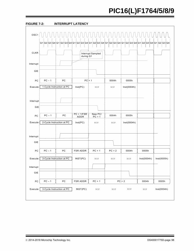
2014-2018 Microchip Technology Inc. DS40001775D-page 98
PIC16(L)F1764/5/8/9
FIGURE 7-2: INTERRUPT LATENCY
Q1 Q2 Q3 Q4 Q1 Q2 Q3 Q4 Q1 Q2 Q3 Q4 Q1 Q2 Q3 Q4 Q1 Q2 Q3 Q4 Q1 Q2 Q3 Q4
OSC1
CLKR
PC 0004h 0005hPC
Inst(0004h)NOP
GIE
Q1 Q2 Q3 Q4Q1 Q2 Q3 Q4
1-Cycle Instruction at PC
PC
Inst(0004h)NOP2-Cycle Instruction at PC
FSR ADDR PC + 1 PC + 2 0004h 0005hPC
Inst(0004h)NOP
GIE
PCPC – 1
3-Cycle Instruction at PC
Execute
Interrupt
Inst(PC)
Interrupt Sampled during Q1
Inst(PC)
PC – 1 PC + 1
NOP
PCNew PC/PC + 1
0005hPC – 1PC + 1/FSR
ADDR0004h
NOP
Interrupt
GIE
Interrupt
INST(PC) NOPNOP
FSR ADDR PC + 1 PC + 2 0004h 0005hPC
Inst(0004h)NOP
GIE
PCPC – 1
3-Cycle Instruction at PC
Interrupt
INST(PC) NOPNOP NOP
Inst(0005h)
Execute
Execute
Execute

2014-2018 Microchip Technology Inc. DS40001775D-page 99
PIC16(L)F1764/5/8/9
FIGURE 7-3: INT PIN INTERRUPT TIMING
Q2Q1 Q3 Q4 Q2Q1 Q3 Q4 Q2Q1 Q3 Q4 Q2Q1 Q3 Q4 Q2Q1 Q3 Q4
OSC1
CLKOUT(3)
INT Pin
INTF
GIE
PC
InstructionFetched
InstructionExecuted
Interrupt Latency(2)
PC PC + 1 PC + 1 0004h 0005h
Inst (0004h) Inst (0005h)
Forced NOP
Inst (PC) Inst (PC + 1)
Inst (PC – 1) Inst (0004h)Forced NOPInst (PC)
—
Note 1: INTF flag is sampled here (every Q1).
2: Asynchronous interrupt latency = 3-5 TCY. Synchronous latency = 3-4 TCY, where TCY = instruction cycle time. Latency is the same whether Inst (PC) is a single cycle or a 2-cycle instruction.
3: CLKOUT not available in all Oscillator modes.
4: For minimum width of INT pulse, refer to the AC specifications in Section 36.0 “Electrical Specifications”.
5: INTF is enabled to be set any time during the Q4-Q1 cycles.
(1)
(4)
(5)
(1)
INSTRUCTION FLOW

2014-2018 Microchip Technology Inc. DS40001775D-page 100
PIC16(L)F1764/5/8/9
7.3 Interrupts During Sleep
Some interrupts can be used to wake from Sleep. Towake from Sleep, the peripheral must be able tooperate without the system clock. The interrupt sourcemust have the appropriate interrupt enable bit(s) setprior to entering Sleep.
On waking from Sleep, if the GIE bit is also set, theprocessor will branch to the interrupt vector. Otherwise,the processor will continue executing instructions afterthe SLEEP instruction. The instruction directly afterthe SLEEP instruction will always be executedbefore branching to the ISR. Refer to Section 8.0“Power-Down Mode (Sleep)” for more details.
7.4 INT Pin
The INT pin can be used to generate an asynchronousedge-triggered interrupt. This interrupt is enabled bysetting the INTE bit of the INTCON register. TheINTEDG bit of the OPTION_REG register determines onwhich edge the interrupt will occur. When the INTEDGbit is set, the rising edge will cause the interrupt. Whenthe INTEDG bit is clear, the falling edge will cause theinterrupt. The INTF bit of the INTCON register will be setwhen a valid edge appears on the INT pin. If the GIE andINTE bits are also set, the processor will redirectprogram execution to the interrupt vector.
7.5 Automatic Context Saving
Upon entering an interrupt, the return PC address issaved on the stack. Additionally, the following registersare automatically saved in the shadow registers:
• W register
• STATUS register (except for TO and PD)
• BSR register
• FSR registers
• PCLATH register
Upon exiting the Interrupt Service Routine, these regis-ters are automatically restored. Any modifications tothese registers during the ISR will be lost. If modifica-tions to any of these registers are desired, the corre-sponding shadow register should be modified and thevalue will be restored when exiting the ISR. Theshadow registers are available in Bank 31 and arereadable and writable. Depending on the user’sapplication, other registers may also need to be saved.

2014-2018 Microchip Technology Inc. DS40001775D-page 101
PIC16(L)F1764/5/8/9
7.6 Register Definitions: Interrupt Control
REGISTER 7-1: INTCON: INTERRUPT CONTROL REGISTER
R/W-0/0 R/W-0/0 R/W-0/0 R/W-0/0 R/W-0/0 R/W-0/0 R/W-0/0 R-0/0
GIE PEIE TMR0IE INTE IOCIE TMR0IF INTF IOCIF(1)
bit 7 bit 0
Legend:
R = Readable bit W = Writable bit
u = Bit is unchanged x = Bit is unknown U = Unimplemented bit, read as ‘0’
‘1’ = Bit is set ‘0’ = Bit is cleared -n/n = Value at POR and BOR/Value at all other Resets
bit 7 GIE: Global Interrupt Enable bit
1 = Enables all active interrupts0 = Disables all interrupts
bit 6 PEIE: Peripheral Interrupt Enable bit
1 = Enables all active peripheral interrupts0 = Disables all peripheral interrupts
bit 5 TMR0IE: Timer0 Overflow Interrupt Enable bit
1 = Enables the Timer0 interrupt0 = Disables the Timer0 interrupt
bit 4 INTE: INT External Interrupt Enable bit
1 = Enables the INT external interrupt0 = Disables the INT external interrupt
bit 3 IOCIE: Interrupt-On-Change Enable bit
1 = Enables the Interrupt-On-Change0 = Disables the Interrupt-On-Change
bit 2 TMR0IF: Timer0 Overflow Interrupt Flag bit
1 = TMR0 register has overflowed0 = TMR0 register did not overflow
bit 1 INTF: INT External Interrupt Flag bit
1 = The INT external interrupt occurred0 = The INT external interrupt did not occur
bit 0 IOCIF: Interrupt-On-Change Interrupt Flag bit(1)
1 = When at least one of the Interrupt-On-Change pins changed state0 = None of the Interrupt-On-Change pins have changed state
Note 1: The IOCIF Flag bit is read-only and cleared when all the Interrupt-On-Change flags in the IOCxF registers have been cleared by software.
Note: Interrupt flag bits are set when an interrupt condition occurs, regardless of the state of its correspondingenable bit or the Global Enable bit, GIE, of the INTCON register. User software should ensure theappropriate interrupt flag bits are clear prior to enabling an interrupt.

2014-2018 Microchip Technology Inc. DS40001775D-page 102
PIC16(L)F1764/5/8/9
REGISTER 7-2: PIE1: PERIPHERAL INTERRUPT ENABLE REGISTER 1
R/W-0/0 R/W-0/0 R/W-0/0 R/W-0/0 R/W-0/0 R/W-0/0 R/W-0/0 R/W-0/0
TMR1GIE ADIE RCIE TXIE SSP1IE CCP1IE TMR2IE TMR1IE
bit 7 bit 0
Legend:
R = Readable bit W = Writable bit
u = Bit is unchanged x = Bit is unknown U = Unimplemented bit, read as ‘0’
‘1’ = Bit is set ‘0’ = Bit is cleared -n/n = Value at POR and BOR/Value at all other Resets
bit 7 TMR1GIE: Timer1 Gate Interrupt Enable bit
1 = Enables the Timer1 gate acquisition interrupt0 = Disables the Timer1 gate acquisition interrupt
bit 6 ADIE: Analog-to-Digital Converter (ADC) Interrupt Enable bit
1 = Enables the ADC interrupt0 = Disables the ADC interrupt
bit 5 RCIE: EUSART Receive Interrupt Enable bit
1 = Enables the EUSART receive interrupt0 = Disables the EUSART receive interrupt
bit 4 TXIE: EUSART Transmit Interrupt Enable bit
1 = Enables the EUSART transmit interrupt0 = Disables the EUSART transmit interrupt
bit 3 SSP1IE: Master Synchronous Serial Port (MSSP) Interrupt Enable bit
1 = Enables the MSSP interrupt0 = Disables the MSSP interrupt
bit 2 CCP1IE: CCP1 Interrupt Enable bit
1 = Enables the CCP1 interrupt0 = Disables the CCP1 interrupt
bit 1 TMR2IE: TMR2 to T2PR Match Interrupt Enable bit
1 = Enables the Timer2 to T2PR match interrupt0 = Disables the Timer2 to T2PR match interrupt
bit 0 TMR1IE: Timer1 Overflow Interrupt Enable bit
1 = Enables the Timer1 overflow interrupt0 = Disables the Timer1 overflow interrupt
Note: Bit PEIE of the INTCON register must be set to enable any peripheral interrupt.
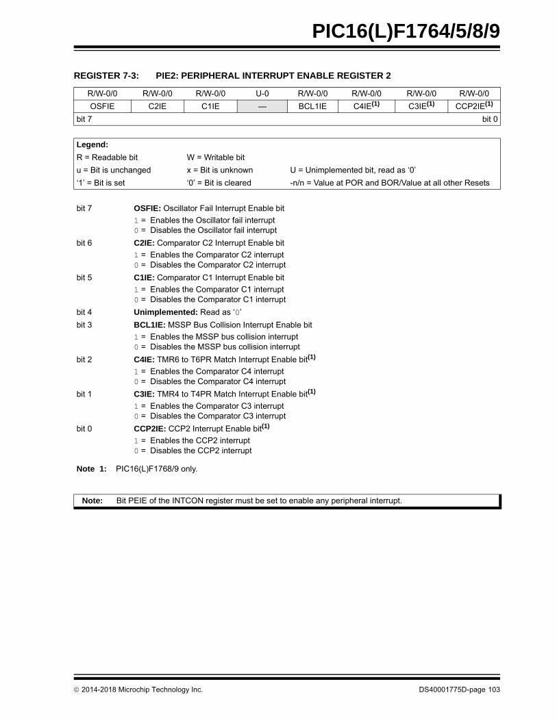
2014-2018 Microchip Technology Inc. DS40001775D-page 103
PIC16(L)F1764/5/8/9
REGISTER 7-3: PIE2: PERIPHERAL INTERRUPT ENABLE REGISTER 2
R/W-0/0 R/W-0/0 R/W-0/0 U-0 R/W-0/0 R/W-0/0 R/W-0/0 R/W-0/0
OSFIE C2IE C1IE — BCL1IE C4IE(1) C3IE(1) CCP2IE(1)
bit 7 bit 0
Legend:
R = Readable bit W = Writable bit
u = Bit is unchanged x = Bit is unknown U = Unimplemented bit, read as ‘0’
‘1’ = Bit is set ‘0’ = Bit is cleared -n/n = Value at POR and BOR/Value at all other Resets
bit 7 OSFIE: Oscillator Fail Interrupt Enable bit
1 = Enables the Oscillator fail interrupt0 = Disables the Oscillator fail interrupt
bit 6 C2IE: Comparator C2 Interrupt Enable bit
1 = Enables the Comparator C2 interrupt0 = Disables the Comparator C2 interrupt
bit 5 C1IE: Comparator C1 Interrupt Enable bit
1 = Enables the Comparator C1 interrupt0 = Disables the Comparator C1 interrupt
bit 4 Unimplemented: Read as ‘0’
bit 3 BCL1IE: MSSP Bus Collision Interrupt Enable bit
1 = Enables the MSSP bus collision interrupt0 = Disables the MSSP bus collision interrupt
bit 2 C4IE: TMR6 to T6PR Match Interrupt Enable bit(1)
1 = Enables the Comparator C4 interrupt0 = Disables the Comparator C4 interrupt
bit 1 C3IE: TMR4 to T4PR Match Interrupt Enable bit(1)
1 = Enables the Comparator C3 interrupt0 = Disables the Comparator C3 interrupt
bit 0 CCP2IE: CCP2 Interrupt Enable bit(1)
1 = Enables the CCP2 interrupt0 = Disables the CCP2 interrupt
Note 1: PIC16(L)F1768/9 only.
Note: Bit PEIE of the INTCON register must be set to enable any peripheral interrupt.

2014-2018 Microchip Technology Inc. DS40001775D-page 104
PIC16(L)F1764/5/8/9
REGISTER 7-4: PIE3: PERIPHERAL INTERRUPT ENABLE REGISTER 3
R/W-0/0 R/W-0/0 R/W-0/0 R/W-0/0 R/W-0/0 R/W-0/0 R/W-0/0 R/W-0/0
PWM6IE(1) PWM5IE COG1IE ZCDIE COG2IE(1) CLC3IE CLC2IE CLC1IE
bit 7 bit 0
Legend:
R = Readable bit W = Writable bit
u = Bit is unchanged x = Bit is unknown U = Unimplemented bit, read as ‘0’
‘1’ = Bit is set ‘0’ = Bit is cleared -n/n = Value at POR and BOR/Value at all other Resets
bit 7 PWM6IE: PWM6 Interrupt Enable bit(1)
1 = PWM6 interrupt is enabled0 = PWM6 interrupt is disabled
bit 6 PWM5IE: PWM5 Interrupt Enable bit
1 = PWM5 interrupt is enabled0 = PWM5 interrupt is disabled
bit 5 COG1IE: COG1 Auto-Shutdown Interrupt Enable bit
1 = COG1 interrupt is enabled0 = COG1 interrupt is disabled
bit 4 ZCDIE: Zero-Cross Detection Interrupt Enable bit
1 = ZCD interrupt is enabled0 = ZCD interrupt is disabled
bit 3 COG2IE: COG2 Auto-Shutdown Interrupt Enable bit(1)
1 = COG2 interrupt is enabled0 = COG2 interrupt is disabled
bit 2 CLC3IE: CLC3 Interrupt Enable bit
1 = CLC3 interrupt is enabled0 = CLC3 interrupt is disabled
bit 1 CLC2IE: CLC2 Interrupt Enable bit
1 = CLC2 interrupt is enabled0 = CLC2 interrupt is disabled
bit 0 CLC1IE: CLC1 Interrupt Enable bit
1 = CLC1 interrupt is enabled0 = CLC1 interrupt is disabled
Note 1: PIC16(L)F1768/9 only.
Note: Bit PEIE of the INTCON register must be set to enable any peripheral interrupt.

2014-2018 Microchip Technology Inc. DS40001775D-page 105
PIC16(L)F1764/5/8/9
REGISTER 7-5: PIR1: PERIPHERAL INTERRUPT REQUEST REGISTER 1
R/W-0/0 R/W-0/0 R-0/0 R-0/0 R/W-0/0 R/W-0/0 R/W-0/0 R/W-0/0
TMR1GIF ADIF RCIF TXIF SSP1IF CCP1IF TMR2IF TMR1IF
bit 7 bit 0
Legend:
R = Readable bit W = Writable bit
u = Bit is unchanged x = Bit is unknown U = Unimplemented bit, read as ‘0’
‘1’ = Bit is set ‘0’ = Bit is cleared -n/n = Value at POR and BOR/Value at all other Resets
bit 7 TMR1GIF: Timer1 Gate Interrupt Flag bit
1 = Interrupt is pending0 = Interrupt is not pending
bit 6 ADIF: Analog-to-Digital Converter (ADC) Interrupt Flag bit
1 = Interrupt is pending0 = Interrupt is not pending
bit 5 RCIF: EUSART Receive Interrupt Flag bit
1 = Interrupt is pending0 = Interrupt is not pending
bit 4 TXIF: EUSART Transmit Interrupt Flag bit
1 = Interrupt is pending0 = Interrupt is not pending
bit 3 SSP1IF: Master Synchronous Serial Port (MSSP) Interrupt Flag bit
1 = Interrupt is pending0 = Interrupt is not pending
bit 2 CCP1IF: CCP1 Interrupt Flag bit
1 = Interrupt is pending0 = Interrupt is not pending
bit 1 TMR2IF: Timer2 to T2PR Interrupt Flag bit
1 = Interrupt is pending0 = Interrupt is not pending
bit 0 TMR1IF: Timer1 Overflow Interrupt Flag bit
1 = Interrupt is pending0 = Interrupt is not pending
Note: Interrupt flag bits are set when an interrupt condition occurs, regardless of the state of its correspondingenable bit or the Global Enable bit, GIE, of the INTCON register. User software should ensure theappropriate interrupt flag bits are clear prior to enabling an interrupt.

2014-2018 Microchip Technology Inc. DS40001775D-page 106
PIC16(L)F1764/5/8/9
REGISTER 7-6: PIR2: PERIPHERAL INTERRUPT REQUEST REGISTER 2
R/W-0/0 R/W-0/0 R/W-0/0 U-0 R/W-0/0 R/W-0/0 R/W-0/0 R/W-0/0
OSFIF C2IF C1IF — BCL1IF C4IF(1) C3IF(1) CCP2IF(1)
bit 7 bit 0
Legend:
R = Readable bit W = Writable bit
u = Bit is unchanged x = Bit is unknown U = Unimplemented bit, read as ‘0’
‘1’ = Bit is set ‘0’ = Bit is cleared -n/n = Value at POR and BOR/Value at all other Resets
bit 7 OSFIF: Oscillator Fail Interrupt Flag bit
1 = Interrupt is pending0 = Interrupt is not pending
bit 6 C2IF: Comparator C2 Interrupt Flag bit
1 = Interrupt is pending0 = Interrupt is not pending
bit 5 C1IF: Comparator C1 Interrupt Flag bit
1 = Interrupt is pending0 = Interrupt is not pending
bit 4 Unimplemented: Read as ‘0’
bit 3 BCL1IF: MSSP Bus Collision Interrupt Flag bit
1 = Interrupt is pending0 = Interrupt is not pending
bit 2 C4IF: Comparator C4 Interrupt Flag bit(1)
1 = Interrupt is pending0 = Interrupt is not pending
bit 1 C3IF: Comparator C3 Interrupt Flag bit(1)
1 = Interrupt is pending0 = Interrupt is not pending
bit 0 CCP2IF: CCP2 Interrupt Flag bit(1)
1 = Interrupt is pending0 = Interrupt is not pending
Note 1: PIC16(L)F1768/9 only.
Note: Interrupt flag bits are set when an interrupt condition occurs, regardless of the state of its correspondingenable bit or the Global Enable bit, GIE, of the INTCON register. User software should ensure theappropriate interrupt flag bits are clear prior to enabling an interrupt.

2014-2018 Microchip Technology Inc. DS40001775D-page 107
PIC16(L)F1764/5/8/9
REGISTER 7-7: PIR3: PERIPHERAL INTERRUPT REQUEST REGISTER 3
R/W-0/0 R/W-0/0 R/W-0/0 R/W-0/0 R/W-0/0 R/W-0/0 R/W-0/0 R/W-0/0
PWM6IF(1) PWM5IF COG1IF ZCDIF COG2IF(1) CLC3IF CLC2IF CLC1IF
bit 7 bit 0
Legend:
R = Readable bit W = Writable bit
u = Bit is unchanged x = Bit is unknown U = Unimplemented bit, read as ‘0’
‘1’ = Bit is set ‘0’ = Bit is cleared -n/n = Value at POR and BOR/Value at all other Resets
bit 7 PWM6IF: PWM6 Interrupt Flag bit(1)
1 = Interrupt is pending0 = Interrupt is not pending
bit 6 PWM5IF: PWM5 Interrupt Flag bit
1 = Interrupt is pending0 = Interrupt is not pending
bit 5 COG1IF: COG1 Auto-Shutdown Interrupt Flag bit
1 = Interrupt is pending0 = Interrupt is not pending
bit 4 ZCDIF: Zero-Cross Detection Interrupt Flag bit
1 = Interrupt is pending0 = Interrupt is not pending
bit 3 COG2IF: COG2 Auto-Shutdown Interrupt Flag bit(1)
1 = Interrupt is pending0 = Interrupt is not pending
bit 2 CLC3IF: CLC3 Interrupt Flag bit
1 = Interrupt is pending0 = Interrupt is not pending
bit 1 CLC2IF: CLC2 Interrupt Flag bit
1 = Interrupt is pending0 = Interrupt is not pending
bit 0 CLC1IF: CLC1 Interrupt Flag bit
1 = Interrupt is pending0 = Interrupt is not pending
Note 1: PIC16(L)F1768/9 only.
Note: Interrupt flag bits are set when an interrupt condition occurs, regardless of the state of its correspondingenable bit or the Global Enable bit, GIE, of the INTCON register. User software should ensure theappropriate interrupt flag bits are clear prior to enabling an interrupt.

2014-2018 Microchip Technology Inc. DS40001775D-page 108
PIC16(L)F1764/5/8/9
TABLE 7-1: SUMMARY OF REGISTERS ASSOCIATED WITH INTERRUPTS
Name Bit 7 Bit 6 Bit 5 Bit 4 Bit 3 Bit 2 Bit 1 Bit 0Register on Page
INTCON GIE PEIE TMR0IE INTE IOCIE TMR0IF INTF IOCIF 101
OPTION_REG WPUEN INTEDG TMR0CS TMR0SE PSA PS<2:0> 214
PIE1 TMR1GIE ADIE RCIE TXIE SSP1IE CCP1IE TMR2IE TMR1IE 102
PIE2 OSFIE C2IE C1IE — BCL1IE C4IE(1) C3IE(1) CCP2IE(1) 103
PIE3 PWM6IE(1) PWM5IE COG1IE ZCDIE COG2IE(1) CLC3IE CLC2IE CLC1IE 104
PIR1 TMR1GIF ADIF RCIF TXIF SSP1IF CCP1IF TMR2IF TMR1IF 105
PIR2 OSFIF C2IF C1IF — BCL1IF C4IF(1) C3IF(1) CCP2IF(1) 106
PIR3 PWM6IF(1) PWM5IF COG1IF ZCDIF COG2IF(1) CLC3IF CLC2IF CLC1IF 107
Legend: — = unimplemented location, read as ‘0’. Shaded cells are not used by interrupts.
Note 1: PIC16(L)F1768/9 only.

2014-2018 Microchip Technology Inc. DS40001775D-page 109
PIC16(L)F1764/5/8/9
8.0 POWER-DOWN MODE (SLEEP)
The Power-Down mode is entered by executing aSLEEP instruction.
Upon entering Sleep mode, the following conditionsexist:
1. WDT will be cleared, but keeps running ifenabled for operation during Sleep.
2. PD bit of the STATUS register is cleared.
3. TO bit of the STATUS register is set.
4. CPU clock is disabled.
5. 31 kHz LFINTOSC is unaffected and peripheralsthat operate from it may continue operation inSleep.
6. Timer1 and peripherals that operate fromTimer1 continue operation in Sleep when theTimer1 clock source selected is:
• LFINTOSC
• T1CKI
• Secondary oscillator
7. ADC is unaffected if the dedicated FRC oscillatoris selected.
8. I/O ports maintain the status they had beforeSLEEP was executed (driving high, low orhigh-impedance).
9. Resets other than WDT are not affected bySleep mode.
Refer to individual chapters for more details onperipheral operation during Sleep.
To minimize current consumption, the followingconditions should be considered:
• I/O pins should not be floating
• External circuitry sinking current from I/O pins
• Internal circuitry sourcing current from I/O pins
• Current draw from pins with internal weak pull-ups
• Modules using 31 kHz LFINTOSC
• Modules using secondary oscillator
I/O pins that are high-impedance inputs should bepulled to VDD or VSS externally to avoid switchingcurrents caused by floating inputs.
Examples of internal circuitry that might be sourcingcurrent include modules such as the DAC and FVRmodules. See Section 17.0 “5-Bit Digital-to-AnalogConverter (DAC) Module” and Section 14.0 “FixedVoltage Reference (FVR)” for more information onthese modules.
8.1 Wake-up from Sleep
The device can wake-up from Sleep through one of thefollowing events:
1. External Reset input on MCLR pin, if enabled.
2. Brown-out Reset (BOR), if enabled.
3. Power-on Reset (POR), if enabled.
4. Watchdog Timer, if enabled.
5. Any external interrupt.
6. Interrupts by peripherals capable of runningduring Sleep (see individual peripheral for moreinformation).
The first three events will cause a device Reset. Thelast three events are considered a continuation ofprogram execution. To determine whether a deviceReset or wake-up event occurred, refer toSection 6.12 “Determining the Cause of a Reset”.
When the SLEEP instruction is being executed, the nextinstruction (PC + 1) is prefetched. For the device towake-up through an interrupt event, the correspondinginterrupt enable bit must be enabled. Wake-up willoccur regardless of the state of the GIE bit. If the GIEbit is disabled, the device continues execution at theinstruction after the SLEEP instruction. If the GIE bit isenabled, the device executes the instruction after theSLEEP instruction, the device will then call the InterruptService Routine. In cases where the execution of theinstruction following SLEEP is not desirable, the usershould insert a NOP after the SLEEP instruction.
The WDT is cleared when the device wakes up fromSleep, regardless of the source of wake-up.

2014-2018 Microchip Technology Inc. DS40001775D-page 110
PIC16(L)F1764/5/8/9
8.1.1 WAKE-UP USING INTERRUPTS
When global interrupts are disabled (GIE cleared) andany interrupt source has both its interrupt enable bitand interrupt flag bit set, one of the following will occur:
• If the interrupt occurs before the execution of a SLEEP instruction:
- SLEEP instruction will execute as a NOP
- WDT and WDT prescaler will not be cleared
- TO bit of the STATUS register will not be set
- PD bit of the STATUS register will not be cleared
• If the interrupt occurs during or after the execution of a SLEEP instruction:
- SLEEP instruction will be completely executed
- Device will immediately wake-up from Sleep
- WDT and WDT prescaler will be cleared
- TO bit of the STATUS register will be set
- PD bit of the STATUS register will be cleared
Even if the flag bits were checked before executing aSLEEP instruction, it may be possible for flag bits tobecome set before the SLEEP instruction completes. Todetermine whether a SLEEP instruction executed, testthe PD bit. If the PD bit is set, the SLEEP instructionwas executed as a NOP.
FIGURE 8-1: WAKE-UP FROM SLEEP THROUGH INTERRUPT
Q1 Q2 Q3 Q4 Q1 Q2 Q3 Q4 Q1 Q1 Q2 Q3 Q4 Q1 Q2 Q3 Q4 Q1 Q2 Q3 Q4 Q1 Q2 Q3 Q4
CLKIN(1)
CLKOUT(2)
Interrupt Flag
GIE bit(INTCON reg.)
Instruction FlowPC
InstructionFetched
InstructionExecuted
PC PC + 1 PC + 2
Inst(PC) = Sleep
Inst(PC – 1)
Inst(PC + 1)
Sleep
Processor inSleep
Inst(PC + 2)
Inst(PC + 1)
Inst(0004h) Inst(0005h)
Inst(0004h)Forced NOP
PC + 2 0004h 0005h
Forced NOP
TOST(3)
PC + 2
Note 1: External clock. High, Medium, Low mode assumed.2: CLKOUT is shown here for timing reference.3: TOST = 1024 TOSC. This delay does not apply to EC, RC and INTOSC Oscillator modes or Two-Speed Start-up (see Section 5.4
“Two-Speed Clock Start-up Mode”.4: GIE = 1 assumed. In this case, after wake-up, the processor calls the ISR at 0004h. If GIE = 0, execution will continue in-line.
Interrupt Latency(4)

2014-2018 Microchip Technology Inc. DS40001775D-page 111
PIC16(L)F1764/5/8/9
8.2 Low-Power Sleep Mode
The PIC16F1764/5/8/9 devices contain an internal LowDropout (LDO) voltage regulator, which allows thedevice I/O pins to operate at voltages up to 5.5V whilethe internal device logic operates at a lower voltage.The LDO and its associated reference circuitry mustremain active when the device is in Sleep mode. ThePIC16F1764/5/8/9 devices allow the user to optimizethe operating current in Sleep, depending on theapplication requirements.
A Low-Power Sleep mode can be selected by settingthe VREGPM bit of the VREGCON register. With thisbit set, the LDO and reference circuitry are placed in alow-power state when the device is in Sleep.
8.2.1 SLEEP CURRENT VS. WAKE-UP TIME
In the default operating mode, the LDO and referencecircuitry remain in the normal configuration while inSleep. The device is able to exit Sleep mode quicklysince all circuits remain active. In Low-Power Sleepmode, when waking up from Sleep, an extra delay timeis required for these circuits to return to the normalconfiguration and stabilize.
The Low-Power Sleep mode is beneficial for applica-tions that stay in Sleep mode for long periods of time.The Normal mode is beneficial for applications thatneed to wake from Sleep quickly and frequently.
8.2.2 PERIPHERAL USAGE IN SLEEP
Some peripherals that can operate in Sleep mode willnot operate properly with the Low-Power Sleep modeselected. The Low-Power Sleep mode is intended foruse with the following peripherals only:
• Brown-out Reset (BOR)
• Watchdog Timer (WDT)
• External interrupt pin/Interrupt-On-Change pins
• Timer1 (with external clock source < 100 kHz)
Note: The PIC16LF1764/5/8/9 devices do nothave a configurable Low-Power Sleepmode. PIC16LF1764/5/8/9 devices areunregulated devices and are always in thelowest power state when in Sleep, with nowake-up time penalty. These devices havea lower maximum VDD and I/O voltage thanthe PIC16F1764/5/8/9. See Section 36.0“Electrical Specifications” for moreinformation.

2014-2018 Microchip Technology Inc. DS40001775D-page 112
PIC16(L)F1764/5/8/9
8.3 Register Definitions: Voltage Regulator Control
TABLE 8-1: SUMMARY OF REGISTERS ASSOCIATED WITH POWER-DOWN MODE
REGISTER 8-1: VREGCON: VOLTAGE REGULATOR CONTROL REGISTER(1)
U-0 U-0 U-0 U-0 U-0 U-0 R/W-0/0 R/W-1/1
— — — — — — VREGPM r
bit 7 bit 0
Legend:
R = Readable bit W = Writable bit r = Reserved bit
u = Bit is unchanged x = Bit is unknown U = Unimplemented bit, read as ‘0’
‘1’ = Bit is set ‘0’ = Bit is cleared -n/n = Value at POR and BOR/Value at all other Resets
bit 7-2 Unimplemented: Read as ‘0’
bit 1 VREGPM: Voltage Regulator Power Mode Selection bit
1 = Low-Power Sleep mode is enabled in Sleep(2)
Draws lowest current in Sleep, slower wake-up.0 = Normal Power mode is enabled in Sleep(2)
Draws higher current in Sleep, faster wake-up.
bit 0 Reserved: Read as ‘1’. Maintain this bit set.
Note 1: PIC16F1764/5/8/9 only.2: See Section 36.0 “Electrical Specifications”.
Name Bit 7 Bit 6 Bit 5 Bit 4 Bit 3 Bit 2 Bit 1 Bit 0Register on Page
INTCON GIE PEIE TMR0IE INTE IOCIE TMR0IF INTF IOCIF 101
IOCAP — — IOCAP<5:0> 162
IOCAN — — IOCAN<5:0> 162
IOCAF — — IOCAF<5:0> 163
IOCBP(1) IOCBP<7:4> — — — — 163
IOCBN(1) IOCBN<7:4> — — — — 164
IOCBF(1) IOCBF<7:4> — — — — 164
IOCCP IOCCP<7:6>(1) IOCCP<5:0> 165
IOCCN IOCCN<7:6>(1) IOCCN<5:0> 165
IOCCF IOCCF<7:6>(1) IOCCF<5:0> 166
PIE1 TMR1GIE ADIE RCIE TXIE SSP1IE CCP1IE TMR2IE TMR1IE 102
PIE2 OSFIE C2IE C1IE — BCL1IE C4IE(1) C3IE(1) CCP2IE(1) 103
PIE3 PWM6IE(1) PWM5IE COG1IE ZCDIE COG2IE(1) CLC3IE CLC2IE CLC1IE 104
PIR1 TMR1GIF ADIF RCIF TXIF SSP1IF CCP1IF TMR2IF TMR1IF 105
PIR2 OSFIF C2IF C1IF — BCL1IF C4IF(1) C3IF(1) CCP2IF(1) 106
PIR3 PWM6IF(1) PWM5IF COG1IF ZCDIF COG2IF(1) CLC3IF CLC2IF CLC1IF 107
STATUS — — — TO PD Z DC C 27
VREGCON(2) — — — — — — VREGPM r 112
WDTCON — — WDTPS<4:0> SWDTEN 115
Legend: — = unimplemented location, read as ‘0’; r = Reserved bit. Shaded cells are not used in Power-Down mode.Note 1: PIC16(L)F1768/9 only.
2: PIC16F1764/5/8/9 only.

2014-2018 Microchip Technology Inc. DS40001775D-page 113
PIC16(L)F1764/5/8/9
9.0 WATCHDOG TIMER (WDT)
The Watchdog Timer is a system timer that generatesa Reset if the firmware does not issue a CLRWDTinstruction within the time-out period. The WatchdogTimer is typically used to recover the system fromunexpected events.
The WDT has the following features:
• Independent clock source• Multiple operating modes:
- WDT is always on- WDT is off when in Sleep- WDT is controlled by software- WDT is always off
• Configurable time-out period is from 1 ms to 256 seconds (nominal)
• Multiple Reset conditions• Operation during Sleep
FIGURE 9-1: WATCHDOG TIMER BLOCK DIAGRAM
WDTE<1:0> = 01
SWDTEN
WDTE<1:0> = 11
WDTE<1:0> = 10
23- it Programmable Prescaler WDTLFINTOSC
WDTPS<4:0>
WDT Time-out
Sleep
Rev. 10-000141A7/30/2013

2014-2018 Microchip Technology Inc. DS40001775D-page 114
PIC16(L)F1764/5/8/9
9.1 Independent Clock Source
The WDT derives its time base from the 31 kHzLFINTOSC internal oscillator. Time intervals in thischapter are based on a nominal interval of 1 ms. SeeTable 36-8 for the LFINTOSC specification.
9.2 WDT Operating Modes
The Watchdog Timer module has four operating modescontrolled by the WDTE<1:0> bits in the ConfigurationWords (see Table 9-1).
9.2.1 WDT IS ALWAYS ON
When the WDTE<1:0> bits of the Configuration Wordsare set to ‘11’, the WDT is always on.
WDT protection is active during Sleep.
9.2.2 WDT IS OFF IN SLEEP
When the WDTE<1:0> bits of the Configuration Wordsare set to ‘10’, the WDT is on, except in Sleep.
WDT protection is not active during Sleep.
9.2.3 WDT CONTROLLED BY SOFTWARE
When the WDTE<1:0> bits of the Configuration Wordsare set to ‘01’, the WDT is controlled by the SWDTENbit of the WDTCON register.
WDT protection is unchanged by Sleep. See Table 9-1for more details.
TABLE 9-1: WDT OPERATING MODES
9.3 Time-out Period
The WDTPS<4:0> bits of the WDTCON register set thetime-out period from 1 ms to 256 seconds (nominal).After a Reset, the default time-out period is twoseconds.
9.4 Clearing the WDT
The WDT is cleared when any of the followingconditions occur:
• Any Reset
• CLRWDT instruction is executed
• Device enters Sleep
• Device wakes up from Sleep
• Oscillator fails
• WDT is disabled
• Oscillator Start-up Timer (OST) is running
See Table 9-2 for more information.
9.5 Operation During Sleep
When the device enters Sleep, the WDT is cleared. Ifthe WDT is enabled during Sleep, the WDT resumescounting.
When the device exits Sleep, the WDT is clearedagain. The WDT remains clear until the OST, ifenabled, completes. See Section 5.0 “OscillatorModule (with Fail-Safe Clock Monitor)” for moreinformation on the OST.
When a WDT time-out occurs while the device is inSleep, no Reset is generated. Instead, the devicewakes up and resumes operation. The TO and PD bitsin the STATUS register are changed to indicate theevent. See the STATUS register (Register 3-1) for moreinformation.
WDTE<1:0> SWDTENDevice Mode
WDT Mode
11 x X Active
10 xAwake Active
Sleep Disabled
011
XActive
0 Disabled
00 x X Disabled
TABLE 9-2: WDT CLEARING CONDITIONS
Conditions WDT
WDTE<1:0> = 00
Cleared
WDTE<1:0> = 01 and SWDTEN = 0
WDTE<1:0> = 10 and enters Sleep
CLRWDT Command
Oscillator Fail is Detected
Exit Sleep + System Clock = T1OSC, EXTRC, INTOSC, EXTCLK
Exit Sleep + System Clock = XT, HS, LP Cleared until the end of OST
Changes INTOSC Divider (IRCFx bits) Unaffected

2014-2018 Microchip Technology Inc. DS40001775D-page 115
PIC16(L)F1764/5/8/9
9.6 Register Definitions: Watchdog Control
REGISTER 9-1: WDTCON: WATCHDOG TIMER CONTROL REGISTER
U-0 U-0 R/W-0/0 R/W-1/1 R/W-0/0 R/W-1/1 R/W-1/1 R/W-0/0
— — WDTPS<4:0>(1) SWDTEN
bit 7 bit 0
Legend:
R = Readable bit W = Writable bit
u = Bit is unchanged x = Bit is unknown U = Unimplemented bit, read as ‘0’
‘1’ = Bit is set ‘0’ = Bit is cleared -m/n = Value at POR and BOR/Value at all other Resets
bit 7-6 Unimplemented: Read as ‘0’
bit 5-1 WDTPS<4:0>: Watchdog Timer Period Select bits(1)
Bit Value = Prescale Rate
11111 = Reserved, results in minimum interval (1:32) • • •10011 = Reserved, results in minimum interval (1:32)10010 = 1:8388608 (223) (Interval 256s nominal)10001 = 1:4194304 (222) (Interval 128s nominal)10000 = 1:2097152 (221) (Interval 64s nominal)01111 = 1:1048576 (220) (Interval 32s nominal)01110 = 1:524288 (219) (Interval 16s nominal)01101 = 1:262144 (218) (Interval 8s nominal)01100 = 1:131072 (217) (Interval 4s nominal)01011 = 1:65536 (Interval 2s nominal) (Reset value)01010 = 1:32768 (Interval 1s nominal)01001 = 1:16384 (Interval 512 ms nominal)01000 = 1:8192 (Interval 256 ms nominal)00111 = 1:4096 (Interval 128 ms nominal)00110 = 1:2048 (Interval 64 ms nominal)00101 = 1:1024 (Interval 32 ms nominal)00100 = 1:512 (Interval 16 ms nominal)00011 = 1:256 (Interval 8 ms nominal)00010 = 1:128 (Interval 4 ms nominal)00001 = 1:64 (Interval 2 ms nominal)00000 = 1:32 (Interval 1 ms nominal)
bit 0 SWDTEN: Software Enable/Disable for Watchdog Timer bit
If WDTE<1:0> = 1x:This bit is ignored.
If WDTE<1:0> = 01:1 = WDT is turned on0 = WDT is turned off
If WDTE<1:0> = 00:This bit is ignored.
Note 1: Times are approximate. WDT time is based on 31 kHz LFINTOSC.

2014-2018 Microchip Technology Inc. DS40001775D-page 116
PIC16(L)F1764/5/8/9
TABLE 9-3: SUMMARY OF REGISTERS ASSOCIATED WITH WATCHDOG TIMER
TABLE 9-4: SUMMARY OF CONFIGURATION WORD WITH WATCHDOG TIMER
Name Bit 7 Bit 6 Bit 5 Bit 4 Bit 3 Bit 2 Bit 1 Bit 0Register on Page
OSCCON SPLLEN IRCF<3:0> — SCS<1:0> 84
STATUS — — — TO PD Z DC C 27
WDTCON — — WDTPS<4:0> SWDTEN 115
Legend: — = unimplemented location, read as ‘0’. Shaded cells are not used by the Watchdog Timer.
Name Bits Bit -/7 Bit -/6 Bit 13/5 Bit 12/4 Bit 11/3 Bit 10/2 Bit 9/1 Bit 8/0Register on Page
CONFIG113:8 — — FCMEN IESO CLKOUTEN BOREN<1:0> —
637:0 CP MCLRE PWRTE WDTE<1:0> FOSC<2:0>
Legend: — = unimplemented location, read as ‘0’. Shaded cells are not used by the Watchdog Timer.

2014-2018 Microchip Technology Inc. DS40001775D-page 117
PIC16(L)F1764/5/8/9
10.0 FLASH PROGRAM MEMORY CONTROL
The Flash program memory is readable and writableduring normal operation over the full VDD range.Program memory is indirectly addressed using SpecialFunction Registers (SFRs). The SFRs used to accessprogram memory are:
• PMCON1
• PMCON2
• PMDATL
• PMDATH
• PMADRL
• PMADRH
When accessing the program memory, thePMDATH:PMDATL register pair forms a 2-byte wordthat holds the 14-bit data for read/write, and thePMADRH:PMADRL register pair forms a 2-byte wordthat holds the 15-bit address of the program memorylocation being read.
The write time is controlled by an on-chip timer. Thewrite/erase voltages are generated by an on-chip chargepump rated to operate over the operating voltage rangeof the device.
The Flash program memory can be protected in twoways: by code protection (CP bit in the ConfigurationWords) and write protection (WRT<1:0> bits in theConfiguration Words).
Code protection (CP = 0) disables access, reading andwriting to the Flash program memory via externaldevice programmers. Code protection does not affectthe self-write and erase functionality. Code protectioncan only be reset by a device programmer performinga bulk erase to the device, clearing all Flash programmemory, Configuration bits and User IDs.(1)
Write protection prohibits self-write and erase to aportion or all of the Flash program memory, as definedby the WRT<1:0> bits. Write protection does not affecta device programmer’s ability to read, write or erasethe device.
10.1 PMADRL and PMADRH Registers
The PMADRH:PMADRL register pair can address upto a maximum of 32K words of program memory. Whenselecting a program address value, the MSB of theaddress is written to the PMADRH register and the LSBis written to the PMADRL register.
10.1.1 PMCON1 AND PMCON2 REGISTERS
PMCON1 is the control register for Flash programmemory accesses.
Control bits, RD and WR, initiate read and write,respectively. These bits cannot be cleared, only set, insoftware. They are cleared by hardware at completionof the read or write operation. The inability to clear theWR bit in software prevents the accidental, prematuretermination of a write operation.
The WREN bit, when set, will allow a write operation tooccur. On power-up, the WREN bit is clear. TheWRERR bit is set when a write operation is interruptedby a Reset during normal operation. In these situations,following Reset, the user can check the WRERR bitand execute the appropriate error handling routine.
The PMCON2 register is a write-only register. Attemptingto read the PMCON2 register will return all ‘0’s.
To enable writes to the program memory, a specificpattern (the unlock sequence), must be written to thePMCON2 register. The required unlock sequenceprevents inadvertent writes to the program memorywrite latches and Flash program memory.
10.2 Flash Program Memory Overview
It is important to understand the Flash program memorystructure for erase and programming operations. Flashprogram memory is arranged in rows. A row consists ofa fixed number of 14-bit program memory words. A rowis the minimum size that can be erased by user software.
After a row has been erased, the user can reprogramall or a portion of this row. Data to be written into theprogram memory row is written to 14-bit wide data writelatches. These write latches are not directly accessibleto the user, but may be loaded via sequential writes tothe PMDATH:PMDATL register pair.
See Table 10-1 for erase row size and the number ofwrite latches for Flash program memory.
Note 1: Code protection of the entire Flashprogram memory array is enabled byclearing the CP bit of the ConfigurationWords.
Note: If the user wants to modify only a portionof a previously programmed row, then thecontents of the entire row must be readand saved in RAM prior to the erase.Then, new data and retained data can bewritten into the write latches to reprogramthe row of Flash program memory. How-ever, any unprogrammed locations can bewritten without first erasing the row. In thiscase, it is not necessary to save andrewrite the other previously programmedlocations.

2014-2018 Microchip Technology Inc. DS40001775D-page 118
PIC16(L)F1764/5/8/9
TABLE 10-1: FLASH MEMORY ORGANIZATION BY DEVICE
10.2.1 READING THE FLASH PROGRAM MEMORY
To read a program memory location, the user must:
1. Write the desired address to thePMADRH:PMADRL register pair.
2. Clear the CFGS bit of the PMCON1 register.
3. Then, set control bit, RD, of the PMCON1 register.
Once the read control bit is set, the Program FlashMemory controller will use the second instruction cycle toread the data. This causes the second instruction,immediately following the “BSF PMCON1,RD” instruction,to be ignored. The data is available in the very next cycle,in the PMDATH:PMDATL register pair; therefore, it canbe read as two bytes in the following instructions.
The PMDATH:PMDATL register pair will hold this valueuntil another read or until it is written to by the user.
FIGURE 10-1: FLASH PROGRAM MEMORY READ FLOWCHART
DeviceRow Erase
(words)
Write Latches (words)
PIC16(L)F1764
32 32PIC16(L)F1765
PIC16(L)F1768
PIC16(L)F1769
Note: The two instructions following a programmemory read are required to be NOPs.This prevents the user from executing a2-cycle instruction on the next instructionafter the RD bit is set.
StartRead Operation
SelectProgram or Configuration Memory
(CFGS)
SelectWord Address
(PMADRH:PMADRL)
Initiate Read operation(RD = 1)
Instruction fetched ignoredNOP execution forced
Data read now inPMDATH:PMDATL
Instruction fetched ignoredNOP execution forced
EndRead Operation
Rev. 10-000046A7/30/2013

2014-2018 Microchip Technology Inc. DS40001775D-page 119
PIC16(L)F1764/5/8/9
FIGURE 10-2: FLASH PROGRAM MEMORY READ CYCLE EXECUTION
EXAMPLE 10-1: FLASH PROGRAM MEMORY READ
Q1 Q2 Q3 Q4 Q1 Q2 Q3 Q4 Q1 Q2 Q3 Q4 Q1 Q2 Q3 Q4 Q1 Q2 Q3 Q4 Q1 Q2 Q3 Q4
BSF PMCON1,RDExecuted Here
INSTR(PC + 1)
Executed Here
PC PC + 1 PMADRH,PMADRL PC + 5Flash ADDR
RD bit
PMDATH,PMDATL
PC + 3 PC + 4
INSTR (PC + 1)
INSTR(PC – 1)Executed Here
INSTR(PC + 3)Executed Here
INSTR(PC + 4)Executed Here
Flash Data
PMDATHPMDATLRegister
INSTR (PC) INSTR (PC + 3) INSTR (PC + 4)
Instruction IgnoredForced NOP
INSTR(PC + 2)
Executed Here
Instruction IgnoredForced NOP
* This code block will read 1 word of program* memory at the memory address:
PROG_ADDR_HI : PROG_ADDR_LO* data will be returned in the variables;* PROG_DATA_HI, PROG_DATA_LO
BANKSEL PMADRL ; Select Bank for PMCON registersMOVLW PROG_ADDR_LO ; MOVWF PMADRL ; Store LSB of addressMOVLW PROG_ADDR_HI ; MOVWF PMADRH ; Store MSB of address
BCF PMCON1,CFGS ; Do not select Configuration SpaceBSF PMCON1,RD ; Initiate readNOP ; Ignored (Figure 10-1)NOP ; Ignored (Figure 10-1)
MOVF PMDATL,W ; Get LSB of wordMOVWF PROG_DATA_LO ; Store in user locationMOVF PMDATH,W ; Get MSB of wordMOVWF PROG_DATA_HI ; Store in user location

2014-2018 Microchip Technology Inc. DS40001775D-page 120
PIC16(L)F1764/5/8/9
10.2.2 FLASH MEMORY UNLOCK SEQUENCE
The unlock sequence is a mechanism that protects theFlash program memory from unintended self-write pro-gramming or erasing. The sequence must be executedand completed without interruption to successfullycomplete any of the following operations:
• Row Erase
• Load program memory write latches
• Write of program memory write latches to program memory
• Write of program memory write latches to User IDs
The unlock sequence consists of the following steps:
1. Write 55h to PMCON2.
2. Write AAh to PMCON2.
3. Set the WR bit in PMCON1.
4. NOP instruction.
5. NOP instruction.
Once the WR bit is set, the processor will always forcetwo NOP instructions. When an erase row or program rowoperation is being performed, the processor will stallinternal operations (typically 2 ms) until the operation iscomplete and then resume with the next instruction.When the operation is loading the program memory writelatches, the processor will always force the two NOPinstructions and continue uninterrupted with the nextinstruction.
Since the unlock sequence must not be interrupted,global interrupts should be disabled prior to the unlocksequence and re-enabled after the unlock sequence iscompleted.
FIGURE 10-3: FLASH PROGRAM MEMORY UNLOCK SEQUENCE FLOWCHART
StartUnlock Sequence
EndUnlock Sequence
Write 0x55 toPMCON2
Write 0xAA toPMCON2
InitiateWrite or Erase operation
(WR = 1)
Instruction fetched ignoredNOP execution forced
Instruction fetched ignoredNOP execution forced
Rev. 10-000047A7/30/2013

2014-2018 Microchip Technology Inc. DS40001775D-page 121
PIC16(L)F1764/5/8/9
10.2.3 ERASING FLASH PROGRAM MEMORY
While executing code, program memory can only beerased by rows. To erase a row:
1. Load the PMADRH:PMADRL register pair withany address within the row to be erased.
2. Clear the CFGS bit of the PMCON1 register.
3. Set the FREE and WREN bits of the PMCON1register.
4. Write 55h, then AAh, to PMCON2 (Flashprogramming unlock sequence).
5. Set control bit WR of the PMCON1 register tobegin the erase operation.
See Example 10-2.
After the “BSF PMCON1,WR” instruction, the processorrequires two cycles to set up the erase operation. Theuser must place two NOP instructions immediately fol-lowing the WR bit set instruction. The processor willhalt internal operations for the typical 2 ms erase time.This is not Sleep mode as the clocks and peripheralswill continue to run. After the erase cycle, the processorwill resume operation with the third instruction after thePMCON1 write instruction.
FIGURE 10-4: FLASH PROGRAM MEMORY ERASE FLOWCHART
Note 1: See Figure 10-3.
StartErase Operation
EndErase Operation
Disable Interrupts(GIE = 0)
SelectProgram or Configuration Memory
(CFGS)
Select Erase Operation(FREE = 1)
Select Row Address(PMADRH:PMADRL)
Enable Write/Erase Operation(WREN = 1)
Unlock Sequence(See Note 1)
Re-enable Interrupts(GIE = 1)
Disable Write/Erase Operation(WREN = 0)
CPU stalls whileErase operation completes
(2 ms typical)
Rev. 10-000048A7/30/2013

2014-2018 Microchip Technology Inc. DS40001775D-page 122
PIC16(L)F1764/5/8/9
EXAMPLE 10-2: ERASING ONE ROW OF PROGRAM MEMORY
; This row erase routine assumes the following:; 1. A valid address within the erase row is loaded in ADDRH:ADDRL; 2. ADDRH and ADDRL are located in shared data memory 0x70 - 0x7F (common RAM)
BCF INTCON,GIE ; Disable ints so required sequences will execute properlyBANKSEL PMADRLMOVF ADDRL,W ; Load lower 8 bits of erase address boundaryMOVWF PMADRLMOVF ADDRH,W ; Load upper 6 bits of erase address boundaryMOVWF PMADRHBCF PMCON1,CFGS ; Not configuration spaceBSF PMCON1,FREE ; Specify an erase operationBSF PMCON1,WREN ; Enable writes
MOVLW 55h ; Start of required sequence to initiate eraseMOVWF PMCON2 ; Write 55hMOVLW 0AAh ;MOVWF PMCON2 ; Write AAhBSF PMCON1,WR ; Set WR bit to begin eraseNOP ; NOP instructions are forced as processor startsNOP ; row erase of program memory.
;; The processor stalls until the erase process is complete; after erase processor continues with 3rd instruction
BCF PMCON1,WREN ; Disable writesBSF INTCON,GIE ; Enable interrupts
Re
qu
ire
dS
eq
ue
nce

2014-2018 Microchip Technology Inc. DS40001775D-page 123
PIC16(L)F1764/5/8/9
10.2.4 WRITING TO FLASH PROGRAM MEMORY
Program memory is programmed using the followingsteps:
1. Load the address in PMADRH:PMADRL of therow to be programmed.
2. Load each write latch with data.
3. Initiate a programming operation.
4. Repeat Steps 1 through 3 until all data is written.
Before writing to program memory, the word(s) to bewritten must be erased or previously unwritten. Programmemory can only be erased one row at a time. Noautomatic erase occurs upon the initiation of the write.
Program memory can be written one or more words ata time. The maximum number of words written at onetime is equal to the number of write latches. SeeFigure 10-5 (row writes to program memory with32 write latches) for more details.
The write latches are aligned to the Flash rowaddress boundary, defined by the upper ten bits ofPMADRH:PMADRL (PMADRH<6:0>:PMADRL<7:5>),with the lower five bits of PMADRL (PMADRL<4:0>)determining the write latch being loaded. Write opera-tions do not cross these boundaries. At the completionof a program memory write operation, the data in thewrite latches is reset to contain 0x3FFF.
The following steps should be completed to load thewrite latches and program a row of program memory.These steps are divided into two parts. First, each writelatch is loaded with data from the PMDATH:PMDATLusing the unlock sequence with LWLO = 1. When thelast word to be loaded into the write latch is ready, theLWLO bit is cleared and the unlock sequenceexecuted. This initiates the programming operation,writing all the latches into Flash program memory.
1. Set the WREN bit of the PMCON1 register.
2. Clear the CFGS bit of the PMCON1 register.
3. Set the LWLO bit of the PMCON1 register.When the LWLO bit of the PMCON1 register is‘1’, the write sequence will only load the writelatches and will not initiate the write to Flashprogram memory.
4. Load the PMADRH:PMADRL register pair withthe address of the location to be written.
5. Load the PMDATH:PMDATL register pair withthe program memory data to be written.
6. Execute the unlock sequence (Section 10.2.2“Flash Memory Unlock Sequence”). The writelatch is now loaded.
7. Increment the PMADRH:PMADRL register pairto point to the next location.
8. Repeat Steps 5 through 7 until all but the lastwrite latch has been loaded.
9. Clear the LWLO bit of the PMCON1 register.When the LWLO bit of the PMCON1 register is‘0’, the write sequence will initiate the write toFlash program memory.
10. Load the PMDATH:PMDATL register pair withthe program memory data to be written.
11. Execute the unlock sequence (Section 10.2.2“Flash Memory Unlock Sequence”). Theentire program memory latch content is nowwritten to Flash program memory.
An example of the complete write sequence is shown inExample 10-3. The initial address is loaded into thePMADRH:PMADRL register pair; the data is loadedusing Indirect Addressing.
Note: The special unlock sequence is requiredto load a write latch with data or initiate aFlash programming operation. If theunlock sequence is interrupted, writing tothe latches or program memory will not beinitiated.
Note: The program memory write latches arereset to the blank state (0x3FFF) at thecompletion of every write or eraseoperation. As a result, it is not necessaryto load all the program memory writelatches. Unloaded latches will remain inthe blank state.
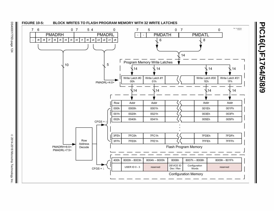
PIC
16(L)F
1764/5/8/9
DS
40
00
17
75
D-p
ag
e 1
24
2
01
4-2
01
8 M
icroch
ip T
ech
no
log
y Inc.
FIGURE 10-5: BLOCK WRITES TO FLASH PROGRAM MEMORY WITH 32 WRITE LATCHES
6 8
14
1414
Write Latch #311Fh
1414
Program Memory Write Latches
14 14 14
PMADRH<6:0>:PMADRL<7:5>
Flash Program Memory
Row
RowAddressDecode
Addr
Write Latch #301Eh
Write Latch #101h
Write Latch #000h
Addr Addr Addr
000h 001Fh001Eh0000h 0001h
001h 003Fh003Eh0020h 0021h
002h 005Fh005Eh0040h 0041h
3FEh 7FDFh7FDEh7FC0h 7FC1h
3FFh 7FFFh7FFEh7FE0h 7FE1h
14
PMADRL<4:0>
400h 8009h - 801Fh8000h - 8003h
ConfigurationWordsUSER ID 0 - 3
8007h – 8008h8006h
DEVICE IDDev / Revreserved reserved
Configuration Memory
CFGS = 0
CFGS = 1
PMADRH PMADRL7 6 0 7 5 4 0
c4 c3 c2 c1 c0r9 r8 r7 r6 r5 r4 r3- r1 r0r2
510
PMDATH PMDATL7 5 0 7 0
--
8004h – 8005h
Rev. 10-000004A7/30/2013

2014-2018 Microchip Technology Inc. DS40001775D-page 125
PIC16(L)F1764/5/8/9
FIGURE 10-6: FLASH PROGRAM MEMORY WRITE FLOWCHART
Disable Interrupts(GIE = 0)
Start Write Operation
Select Program or Config. Memory
(CFGS)
Select Row Address(PMADRH:PMADRL)
Select Write Operation(FREE = 0)
Enable Write/Erase Operation (WREN = 1)
Unlock Sequence(Figure x-x)
Disable Write/Erase Operation
(WREN = 0)
Re-enable Interrupts(GIE = 1)
End Write Operation
No delay when writing to Program Memory Latches
Determine number of words to be written into Program or
Configuration Memory. The number of words cannot exceed the number of words
per row.(word_cnt) Load the value to write
(PMDATH:PMDATL)
Update the word counter (word_cnt--)
Last word to write ?
Increment Address(PMADRH:PMADRL++)
Unlock Sequence(Figure x-x)
CPU stalls while Write operation completes
(2ms typical)
Load Write Latches Only(LWLO = 1)
Write Latches to Flash(LWLO = 0)
No
Yes Figure 10-3
Figure 10-3

2014-2018 Microchip Technology Inc. DS40001775D-page 126
PIC16(L)F1764/5/8/9
EXAMPLE 10-3: WRITING TO FLASH PROGRAM MEMORY
; This write routine assumes the following:; 1. 64 bytes of data are loaded, starting at the address in DATA_ADDR; 2. Each word of data to be written is made up of two adjacent bytes in DATA_ADDR,; stored in little endian format; 3. A valid starting address (the least significant bits = 00000) is loaded in ADDRH:ADDRL; 4. ADDRH and ADDRL are located in shared data memory 0x70 - 0x7F (common RAM);
BCF INTCON,GIE ; Disable ints so required sequences will execute properlyBANKSEL PMADRH ; Bank 3MOVF ADDRH,W ; Load initial addressMOVWF PMADRH ;MOVF ADDRL,W ;MOVWF PMADRL ;MOVLW LOW DATA_ADDR ; Load initial data addressMOVWF FSR0L ;MOVLW HIGH DATA_ADDR ; Load initial data addressMOVWF FSR0H ;BCF PMCON1,CFGS ; Not configuration spaceBSF PMCON1,WREN ; Enable writesBSF PMCON1,LWLO ; Only Load Write Latches
LOOPMOVIW FSR0++ ; Load first data byte into lowerMOVWF PMDATL ;MOVIW FSR0++ ; Load second data byte into upperMOVWF PMDATH ;
MOVF PMADRL,W ; Check if lower bits of address are '00000'XORLW 0x1F ; Check if we're on the last of 32 addressesANDLW 0x1F ;BTFSC STATUS,Z ; Exit if last of 32 words,GOTO START_WRITE ;
MOVLW 55h ; Start of required write sequence:MOVWF PMCON2 ; Write 55hMOVLW 0AAh ;MOVWF PMCON2 ; Write AAhBSF PMCON1,WR ; Set WR bit to begin writeNOP ; NOP instructions are forced as processor
; loads program memory write latchesNOP ;
INCF PMADRL,F ; Still loading latches Increment addressGOTO LOOP ; Write next latches
START_WRITEBCF PMCON1,LWLO ; No more loading latches - Actually start Flash program
; memory write
MOVLW 55h ; Start of required write sequence:MOVWF PMCON2 ; Write 55hMOVLW 0AAh ;MOVWF PMCON2 ; Write AAhBSF PMCON1,WR ; Set WR bit to begin writeNOP ; NOP instructions are forced as processor writes
; all the program memory write latches simultaneouslyNOP ; to program memory.
; After NOPs, the processor; stalls until the self-write process in complete; after write processor continues with 3rd instruction
BCF PMCON1,WREN ; Disable writesBSF INTCON,GIE ; Enable interrupts
Re
qu
ire
dS
eq
ue
nce
Re
qu
ire
dS
eq
ue
nce

2014-2018 Microchip Technology Inc. DS40001775D-page 127
PIC16(L)F1764/5/8/9
10.3 Modifying Flash Program Memory
When modifying existing data in a program memoryrow, and data within that row must be preserved, it mustfirst be read and saved in a RAM image. Programmemory is modified using the following steps:
1. Load the starting address of the row to bemodified.
2. Read the existing data from the row into a RAMimage.
3. Modify the RAM image to contain the new datato be written into program memory.
4. Load the starting address of the row to berewritten.
5. Erase the program memory row.
6. Load the write latches with data from the RAMimage.
7. Initiate a programming operation.
FIGURE 10-7: FLASH PROGRAM MEMORY MODIFY FLOWCHART
StartModify Operation
EndModify Operation
Read Operation(See Note 1)
An image of the entire rowread must be stored in RAM
Erase Operation(See Note 2)
Modify ImageThe words to be modified arechanged in the RAM image
Write OperationUse RAM image
(See Note 3)
Rev. 10-000050A7/30/2013
Note 1: See Figure 10-1.
2: See Figure 10-4.
3: See Figure 10-6.

2014-2018 Microchip Technology Inc. DS40001775D-page 128
PIC16(L)F1764/5/8/9
10.4 User ID, Device ID and Configuration Word Access
Instead of accessing program memory, the User IDs,Device ID/Revision ID and Configuration Words can beaccessed when CFGS = 1 in the PMCON1 register.This is the region that would be pointed to byPC<15> = 1, but not all addresses are accessible.Different access may exist for reads and writes. Referto Table 10-2.
When read access is initiated on an address outside theparameters listed in Table 10-2, the PMDATH:PMDATLregister pair is cleared, reading back ‘0’s.
TABLE 10-2: USER ID, DEVICE ID AND CONFIGURATION WORD ACCESS (CFGS = 1)
EXAMPLE 10-4: CONFIGURATION WORD AND DEVICE ID ACCESS
Address Function Read Access Write Access
8000h-8003h User IDs Yes Yes
8005h-8006h Device ID/Revision ID Yes No
8007h-8008h Configuration Words 1 and 2 Yes No
* This code block will read 1 word of program memory at the memory address:* PROG_ADDR_LO (must be 00h-08h) data will be returned in the variables;* PROG_DATA_HI, PROG_DATA_LO
BANKSEL PMADRL ; Select correct BankMOVLW PROG_ADDR_LO ; MOVWF PMADRL ; Store LSB of addressCLRF PMADRH ; Clear MSB of address
BSF PMCON1,CFGS ; Select Configuration Space BCF INTCON,GIE ; Disable interruptsBSF PMCON1,RD ; Initiate readNOP ; Executed (See Figure 10-2)NOP ; Ignored (See Figure 10-2)BSF INTCON,GIE ; Restore interrupts
MOVF PMDATL,W ; Get LSB of wordMOVWF PROG_DATA_LO ; Store in user locationMOVF PMDATH,W ; Get MSB of wordMOVWF PROG_DATA_HI ; Store in user location

2014-2018 Microchip Technology Inc. DS40001775D-page 129
PIC16(L)F1764/5/8/9
10.5 Write/Verify
It is considered good programming practice to verify thatprogram memory writes agree with the intended value.Since program memory is stored as a full page then thestored program memory contents are compared with theintended data stored in RAM after the last write iscomplete.
FIGURE 10-8: FLASH PROGRAM MEMORY VERIFY FLOWCHART
StartVerify Operation
This routine assumes that the lastrow of data written was from an
image saved on RAM. This imagewill be used to verify the data
currently stored in Flash ProgramMemory
FailVerify Operation
Last word ?
PMDAT =RAM image ?
Read Operation(See Note 1)
EndVerify Operation
No
No
Yes
Yes
Rev. 10-000051A7/30/2013
Note 1: See Figure 10-1.

2014-2018 Microchip Technology Inc. DS40001775D-page 130
PIC16(L)F1764/5/8/9
10.6 Register Definitions: Flash Program Memory Control
REGISTER 10-1: PMDATL: PROGRAM MEMORY DATA LOW BYTE REGISTER
R/W-x/u R/W-x/u R/W-x/u R/W-x/u R/W-x/u R/W-x/u R/W-x/u R/W-x/u
PMDAT<7:0>
bit 7 bit 0
Legend:
R = Readable bit W = Writable bit
u = Bit is unchanged x = Bit is unknown U = Unimplemented bit, read as ‘0’
‘1’ = Bit is set ‘0’ = Bit is cleared -n/n = Value at POR and BOR/Value at all other Resets
bit 7-0 PMDAT<7:0>: Read/Write Value for Least Significant bits of Program Memory bits
REGISTER 10-2: PMDATH: PROGRAM MEMORY DATA HIGH BYTE REGISTER
U-0 U-0 R/W-x/u R/W-x/u R/W-x/u R/W-x/u R/W-x/u R/W-x/u
— — PMDAT<13:8>
bit 7 bit 0
Legend:
R = Readable bit W = Writable bit
u = Bit is unchanged x = Bit is unknown U = Unimplemented bit, read as ‘0’
‘1’ = Bit is set ‘0’ = Bit is cleared -n/n = Value at POR and BOR/Value at all other Resets
bit 7-6 Unimplemented: Read as ‘0’
bit 5-0 PMDAT<13:8>: Read/Write Value for Most Significant bits of Program Memory bits

2014-2018 Microchip Technology Inc. DS40001775D-page 131
PIC16(L)F1764/5/8/9
REGISTER 10-3: PMADRL: PROGRAM MEMORY ADDRESS LOW BYTE REGISTER
R/W-0/0 R/W-0/0 R/W-0/0 R/W-0/0 R/W-0/0 R/W-0/0 R/W-0/0 R/W-0/0
PMADR<7:0>
bit 7 bit 0
Legend:
R = Readable bit W = Writable bit
u = Bit is unchanged x = Bit is unknown U = Unimplemented bit, read as ‘0’
‘1’ = Bit is set ‘0’ = Bit is cleared -n/n = Value at POR and BOR/Value at all other Resets
bit 7-0 PMADR<7:0>: Specifies the Least Significant bits for Program Memory Address bits
REGISTER 10-4: PMADRH: PROGRAM MEMORY ADDRESS HIGH BYTE REGISTER
U-1 R/W-0/0 R/W-0/0 R/W-0/0 R/W-0/0 R/W-0/0 R/W-0/0 R/W-0/0
—(1) PMADR<14:8>
bit 7 bit 0
Legend:
R = Readable bit W = Writable bit
u = Bit is unchanged x = Bit is unknown U = Unimplemented bit, read as ‘0’
‘1’ = Bit is set ‘0’ = Bit is cleared -n/n = Value at POR and BOR/Value at all other Resets
bit 7 Unimplemented: Read as ‘1’
bit 6-0 PMADR<14:8>: Specifies the Most Significant bits for Program Memory Address bits
Note 1: Unimplemented, read as ‘1’.

2014-2018 Microchip Technology Inc. DS40001775D-page 132
PIC16(L)F1764/5/8/9
REGISTER 10-5: PMCON1: PROGRAM MEMORY CONTROL 1 REGISTER
U-1 R/W-0/0 R/W-0/0 R/W/HC-0/0 R/W/HC-x/q(2) R/W-0/0 R/S/HC-0/0 R/S/HC-0/0
—(1) CFGS LWLO(3) FREE WRERR WREN WR RD
bit 7 bit 0
Legend:
R = Readable bit W = Writable bit U = Unimplemented bit, read as ‘0’
S = Settable Only bit x = Bit is unknown -n/n = Value at POR and BOR/Value at all other Resets
‘1’ = Bit is set ‘0’ = Bit is cleared HC = Hardware Clearable bit
bit 7 Unimplemented: Read as ‘1’
bit 6 CFGS: Configuration Select bit
1 = Accesses Configuration, User ID and Device ID registers0 = Accesses Flash program memory
bit 5 LWLO: Load Write Latches Only bit(3)
1 = Only the addressed program memory write latch is loaded/updated on the next WR command0 = The addressed program memory write latch is loaded/updated and a write of all program memory
write latches will be initiated on the next WR command
bit 4 FREE: Program Flash Erase Enable bit
1 = Performs an erase operation on the next WR command (hardware cleared upon completion)0 = Performs a write operation on the next WR command
bit 3 WRERR: Program/Erase Error Flag bit(2)
1 = Condition indicates an improper program or erase sequence attempt, or termination (bit is setautomatically on any set attempt (writes ‘1’) of the WR bit)
0 = The program or erase operation completed normally
bit 2 WREN: Program/Erase Enable bit
1 = Allows program/erase cycles0 = Inhibits programming/erasing of program Flash
bit 1 WR: Write Control bit
1 = Initiates a Flash program/erase operation The operation is self-timed and the bit is cleared by hardware once operation is complete. The WR bit can only be set (not cleared) in software.
0 = Program/erase operation to the Flash is complete and inactive
bit 0 RD: Read Control bit
1 = Initiates a program Flash read Read takes one cycle. RD is cleared in hardware. The RD bit can only be set (not cleared) in software.
0 = Does not initiate a program Flash read
Note 1: Unimplemented bit, read as ‘1’.2: The WRERR bit is automatically set by hardware when a program memory write or erase operation is
started (WR = 1).3: The LWLO bit is ignored during a program memory erase operation (FREE = 1).

2014-2018 Microchip Technology Inc. DS40001775D-page 133
PIC16(L)F1764/5/8/9
TABLE 10-3: SUMMARY OF REGISTERS ASSOCIATED WITH FLASH PROGRAM MEMORY
TABLE 10-4: SUMMARY OF CONFIGURATION WORD WITH FLASH PROGRAM MEMORY
REGISTER 10-6: PMCON2: PROGRAM MEMORY CONTROL 2 REGISTER
W-0/0 W-0/0 W-0/0 W-0/0 W-0/0 W-0/0 W-0/0 W-0/0
Program Memory Control Register 2
bit 7 bit 0
Legend:
R = Readable bit W = Writable bit
S = Bit can only be set x = Bit is unknown U = Unimplemented bit, read as ‘0’
‘1’ = Bit is set ‘0’ = Bit is cleared -n/n = Value at POR and BOR/Value at all other Resets
bit 7-0 Program Memory Control 2: Flash Memory Unlock Pattern bits
To unlock writes, 55h must be written first, followed by AAh, before setting the WR bit of the PMCON1register. The value written to this register is used to unlock the writes. There are specific timingrequirements on these writes.
Name Bit 7 Bit 6 Bit 5 Bit 4 Bit 3 Bit 2 Bit 1 Bit 0Register on Page
INTCON GIE PEIE TMR0IE INTE IOCIE TMR0IF INTF IOCIF 101
PMCON1 —(1) CFGS LWLO FREE WRERR WREN WR RD 132
PMCON2 Program Memory Control Register 2 133
PMADRL PMADRL<7:0> 131
PMADRH —(1) PMADRH<6:0> 131
PMDATL PMDATL<7:0> 130
PMDATH — — PMDATH<5:0> 130
Legend: — = unimplemented location, read as ‘0’. Shaded cells are not used by Flash program memory.
Note 1: Unimplemented, read as ‘1’.
Name Bits Bit -/7 Bit -/6 Bit 13/5 Bit 12/4 Bit 11/3 Bit 10/2 Bit 9/1 Bit 8/0Register on Page
CONFIG113:8 — — FCMEN IESO CLKOUTEN BOREN<1:0> —
637:0 CP MCLRE PWRTE WDTE<1:0> FOSC<2:0>
CONFIG213:8 — — LVP DEBUG LPBOR BORV STVREN PLLEN 65
7:0 ZCD — — — — PPS1WAY WRT<1:0>
Legend: — = unimplemented location, read as ‘0’. Shaded cells are not used by Flash program memory.

2014-2018 Microchip Technology Inc. DS40001775D-page 134
PIC16(L)F1764/5/8/9
11.0 I/O PORTS
Each port has six standard registers for its operation.These registers are:
• TRISx registers (Data Direction)
• PORTx registers (reads the levels on the pins of the device)
• LATx registers (Output Latch)
• INLVLx (Input Level Control)
• ODCONx registers (Open-Drain)
• SLRCONx registers (Slew Rate
Some ports may have one or more of the followingadditional registers. These registers are:
• ANSELx (Analog Select)
• WPUx (Weak Pull-up)
In general, when a peripheral is enabled on a port pin,that pin cannot be used as a general purpose output.However, the pin can still be read.
TABLE 11-1: PORT AVAILABILITY PER DEVICE
The Data Latch (LATx registers) is useful forRead-Modify-Write operations on the value that the I/Opins are driving.
A write operation to the LATx register has the sameeffect as a write to the corresponding PORTx register.A read of the LATx register reads the values held in theI/O PORT latches, while a read of the PORTx registerreads the actual I/O pin value.
Ports that support analog inputs have an associatedANSELx register. When an ANSEL bit is set, the digitalinput buffer associated with that bit is disabled.Disabling the input buffer prevents analog signal levelson the pin between a logic high and low from causingexcessive current in the logic input circuitry. Asimplified model of a generic I/O port, without theinterfaces to other peripherals, is shown in Figure 11-1.
FIGURE 11-1: GENERIC I/O PORT OPERATION
11.1 PORTA Registers
11.1.1 DATA REGISTER
PORTA is a 6-bit wide, bidirectional port. Thecorresponding Data Direction register is TRISA(Register 11-2). Setting a TRISA bit (= 1) will make thecorresponding PORTA pin an input (i.e., disables theoutput driver). Clearing a TRISA bit (= 0) will make thecorresponding PORTA pin an output (i.e., enables theoutput driver and puts the contents of the output latchon the selected pin). The exception is RA3, which isinput-only and its TRISA bit will always read as ‘1’.Example 11-1 shows how to initialize PORTA.
Reading the PORTA register (Register 11-1) reads thestatus of the pins, whereas writing to it, will write to thePORT latch. All write operations are Read-Modify-Writeoperations. Therefore, a write to a port implies that theport pins are read, this value is modified and then writtento the PORTA Data Latch (LATA).
11.1.2 DIRECTION CONTROL
The TRISA register (Register 11-2) controls thePORTA pin output drivers, even when they are beingused as analog inputs. The user should ensure the bitsin the TRISA register are maintained set when usingthem as analog inputs. I/O pins configured as analoginputs always read ‘0’.
Device
PO
RTA
PO
RT
B
PO
RT
C
PIC16(L)F1764 ● ●
PIC16(L)F1765 ● ●
PIC16(L)F1768 ● ● ●
PIC16(L)F1769 ● ● ●
Write LATxWrite PORTx
Data bus
Read PORTx
To digital peripherals
To analog peripherals
Data Register
TRISx
VSS
I/O pin
ANSELx
D Q
CK
Read LATx
VDD
Rev. 10-000052A7/30/2013

2014-2018 Microchip Technology Inc. DS40001775D-page 135
PIC16(L)F1764/5/8/9
11.1.3 OPEN-DRAIN CONTROL
The ODCONA register (Register 11-6) controls theopen-drain feature of the port. Open-drain operation isindependently selected for each pin. When anODCONA bit is set, the corresponding port outputbecomes an open-drain driver, capable of sinkingcurrent only. When an ODCONA bit is cleared, thecorresponding port output pin is the standard push-pulldrive capable of sourcing and sinking current.
11.1.4 SLEW RATE CONTROL
The SLRCONA register (Register 11-7) controls theslew rate option for each port pin. Slew rate control isindependently selectable for each port pin. When anSLRCONA bit is set, the corresponding port pin drive isslew rate limited. When an SLRCONA bit is cleared,the corresponding port pin drive slews at the maximumrate possible.
11.1.5 INPUT THRESHOLD CONTROL
The INLVLA register (Register 11-8) controls the inputvoltage threshold for each of the available PORTA inputpins. A selection between the Schmitt Trigger CMOS orthe TTL compatible thresholds is available. The inputthreshold is important in determining the value of a readof the PORTA register and also the level at which anInterrupt-On-Change occurs, if that feature is enabled.See Table 36-4 for more information on threshold levels.
11.1.6 ANALOG CONTROL
The ANSELA register (Register 11-4) is used toconfigure the Input mode of an I/O pin to analog.Setting the appropriate ANSELA bit high will cause alldigital reads on the pin to be read as ‘0’ and allowanalog functions on the pin to operate correctly.
The state of the ANSELA bits has no effect on digital out-put functions. A pin with TRISx clear and ANSELx setwill still operate as a digital output, but the Input modewill be analog. This can cause unexpected behaviorwhen executing Read-Modify-Write instructions on theaffected port.
EXAMPLE 11-1: INITIALIZING PORTA
11.1.7 PORTA FUNCTIONS AND OUTPUT PRIORITIES
Each PORTA pin is multiplexed with other functions.
Each pin defaults to the PORT latch data after Reset.Other functions are selected with the Peripheral PinSelect (PPS) logic. See Section 12.0 “Peripheral PinSelect (PPS) Module” for more information.
Analog input functions, such as the ADC andcomparator inputs, are not shown in the Peripheral PinSelect lists. These inputs are active when the I/O pin isset for Analog mode using the ANSELA register. Digitaloutput functions may continue to control the pin when itis in Analog mode.
Note: Changing the input threshold selectionshould be performed while all peripheralmodules are disabled. Changing the thresh-old level during the time a module is activemay inadvertently generate a transitionassociated with an input pin, regardless ofthe actual voltage level on that pin.
Note: The ANSELA bits default to the Analogmode after Reset. To use any pins asdigital general purpose or peripheralinputs, the corresponding ANSELA bitsmust be initialized to ‘0’ by user software.
; This code example illustrates; initializing the PORTA register. The ; other ports are initialized in the same; manner.
BANKSEL PORTA ;CLRF PORTA ;Init PORTABANKSEL LATA ;Data LatchCLRF LATA ;BANKSEL ANSELA ;CLRF ANSELA ;digital I/OBANKSEL TRISA ;MOVLW B'00111000' ;Set RA<5:3> as inputsMOVWF TRISA ;and set RA<2:0> as
;outputs
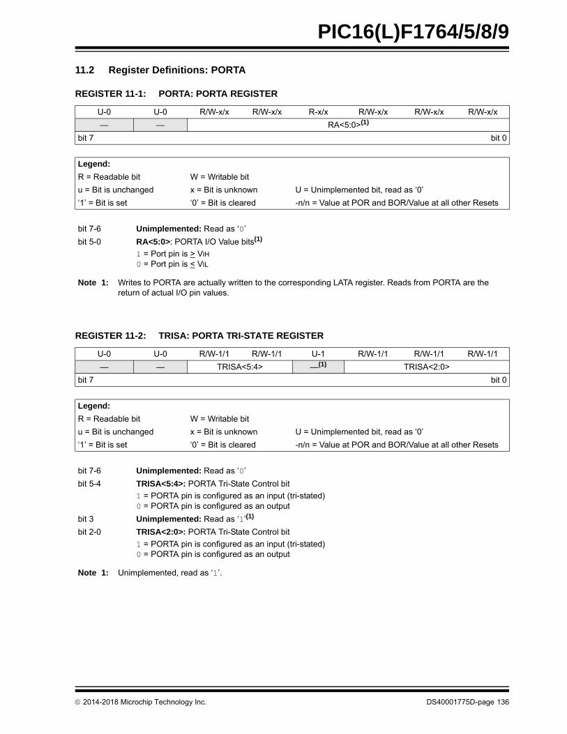
2014-2018 Microchip Technology Inc. DS40001775D-page 136
PIC16(L)F1764/5/8/9
11.2 Register Definitions: PORTA
REGISTER 11-1: PORTA: PORTA REGISTER
U-0 U-0 R/W-x/x R/W-x/x R-x/x R/W-x/x R/W-x/x R/W-x/x
— — RA<5:0>(1)
bit 7 bit 0
Legend:
R = Readable bit W = Writable bit
u = Bit is unchanged x = Bit is unknown U = Unimplemented bit, read as ‘0’
‘1’ = Bit is set ‘0’ = Bit is cleared -n/n = Value at POR and BOR/Value at all other Resets
bit 7-6 Unimplemented: Read as ‘0’
bit 5-0 RA<5:0>: PORTA I/O Value bits(1)
1 = Port pin is > VIH
0 = Port pin is < VIL
Note 1: Writes to PORTA are actually written to the corresponding LATA register. Reads from PORTA are the return of actual I/O pin values.
REGISTER 11-2: TRISA: PORTA TRI-STATE REGISTER
U-0 U-0 R/W-1/1 R/W-1/1 U-1 R/W-1/1 R/W-1/1 R/W-1/1
— — TRISA<5:4> —(1) TRISA<2:0>
bit 7 bit 0
Legend:
R = Readable bit W = Writable bit
u = Bit is unchanged x = Bit is unknown U = Unimplemented bit, read as ‘0’
‘1’ = Bit is set ‘0’ = Bit is cleared -n/n = Value at POR and BOR/Value at all other Resets
bit 7-6 Unimplemented: Read as ‘0’
bit 5-4 TRISA<5:4>: PORTA Tri-State Control bit
1 = PORTA pin is configured as an input (tri-stated)0 = PORTA pin is configured as an output
bit 3 Unimplemented: Read as ‘1’(1)
bit 2-0 TRISA<2:0>: PORTA Tri-State Control bit
1 = PORTA pin is configured as an input (tri-stated)0 = PORTA pin is configured as an output
Note 1: Unimplemented, read as ‘1’.

2014-2018 Microchip Technology Inc. DS40001775D-page 137
PIC16(L)F1764/5/8/9
REGISTER 11-3: LATA: PORTA DATA LATCH REGISTER
U-0 U-0 R/W-x/u R/W-x/u U-0 R/W-x/u R/W-x/u R/W-x/u
— — LATA<5:4>(1) — LATA<2:0>(1)
bit 7 bit 0
Legend:
R = Readable bit W = Writable bit
u = Bit is unchanged x = Bit is unknown U = Unimplemented bit, read as ‘0’
‘1’ = Bit is set ‘0’ = Bit is cleared -n/n = Value at POR and BOR/Value at all other Resets
bit 7-6 Unimplemented: Read as ‘0’
bit 5-4 LATA<5:4>: RA<5:4> Output Latch Value bits(1)
bit 3 Unimplemented: Read as ‘0’
bit 2-0 LATA<2:0>: RA<2:0> Output Latch Value bits(1)
Note 1: Writes to PORTA are actually written to the corresponding LATA register. Reads from PORTA are the return of actual I/O pin values.
REGISTER 11-4: ANSELA: PORTA ANALOG SELECT REGISTER
U-0 U-0 U-0 R/W-1/1 U-0 R/W-1/1 R/W-1/1 R/W-1/1
— — — ANSA4 — ANSA<2:0>
bit 7 bit 0
Legend:
R = Readable bit W = Writable bit
u = Bit is unchanged x = Bit is unknown U = Unimplemented bit, read as ‘0’
‘1’ = Bit is set ‘0’ = Bit is cleared -n/n = Value at POR and BOR/Value at all other Resets
bit 7-5 Unimplemented: Read as ‘0’
bit 4 ANSA4: Analog Select Between Analog or Digital Function on RA4 Pin bit
1 = Analog input; pin is assigned as an analog input, digital input buffer is disabled(1)
0 = Digital I/O; pin is assigned to port or digital special function
bit 3 Unimplemented: Read as ‘0’
bit 2-0 ANSA<2:0>: Analog Select Between Analog or Digital Function on RA<2:0> Pins bits
1 = Analog input; pin is assigned as an analog input, digital input buffer is disabled(1)
0 = Digital I/O; pin is assigned to port or digital special function
Note 1: When setting a pin to an analog input, the corresponding TRISx bit must be set to Input mode in order to allow external control of the voltage on the pin.

2014-2018 Microchip Technology Inc. DS40001775D-page 138
PIC16(L)F1764/5/8/9
REGISTER 11-5: WPUA: WEAK PULL-UP PORTA REGISTER
U-0 U-0 R/W-1/1 R/W-1/1 R/W-1/1 R/W-1/1 R/W-1/1 R/W-1/1
— — WPUA<5:0>(1,2)
bit 7 bit 0
Legend:
R = Readable bit W = Writable bit
u = Bit is unchanged x = Bit is unknown U = Unimplemented bit, read as ‘0’
‘1’ = Bit is set ‘0’ = Bit is cleared -n/n = Value at POR and BOR/Value at all other Resets
bit 7-6 Unimplemented: Read as ‘0’
bit 5-0 WPUA<5:0>: Weak Pull-up PORTA Register bits(1,2)
1 = Pull-up is enabled0 = Pull-up is disabled
Note 1: The global WPUEN bit of the OPTION_REG register must be cleared for individual pull-ups to be enabled.
2: The weak pull-up device is automatically disabled if the pin is configured as an output.
REGISTER 11-6: ODCONA: PORTA OPEN-DRAIN CONTROL REGISTER
U-0 U-0 R/W-0/0 R/W-0/0 U-0 R/W-0/0 R/W-0/0 R/W-0/0
— — ODA<5:4> — ODA<2:0>
bit 7 bit 0
Legend:
R = Readable bit W = Writable bit
u = Bit is unchanged x = Bit is unknown U = Unimplemented bit, read as ‘0’
‘1’ = Bit is set ‘0’ = Bit is cleared -n/n = Value at POR and BOR/Value at all other Resets
bit 7-6 Unimplemented: Read as ‘0’
bit 5-4 ODA<5:4>: PORTA Open-Drain Enable bits
For RA<5:4> Pins:1 = Port pins operate as open-drain drive (sink current only)0 = Port pins operate as standard push-pull drive (source and sink current)
bit 3 Unimplemented: Read as ‘0’
bit 2-0 ODA<2:0>: PORTA Open-Drain Enable bits
For RA<2:0> Pins:1 = Port pins operate as open-drain drive (sink current only)0 = Port pins operate as standard push-pull drive (source and sink current)

2014-2018 Microchip Technology Inc. DS40001775D-page 139
PIC16(L)F1764/5/8/9
REGISTER 11-7: SLRCONA: PORTA SLEW RATE CONTROL REGISTER
U-0 U-0 R/W-1/1 R/W-1/1 U-0 R/W-1/1 R/W-1/1 R/W-1/1
— — SLRA<5:4> — SLRA<2:0>
bit 7 bit 0
Legend:
R = Readable bit W = Writable bit
u = Bit is unchanged x = Bit is unknown U = Unimplemented bit, read as ‘0’
‘1’ = Bit is set ‘0’ = Bit is cleared -n/n = Value at POR and BOR/Value at all other Resets
bit 7-6 Unimplemented: Read as ‘0’
bit 5-4 SLRA<5:4>: PORTA Slew Rate Enable bits
For RA<5:4> Pins:1 = Port pin slew rate is limited0 = Port pin slews at maximum rate
bit 3 Unimplemented: Read as ‘0’
bit 2-0 SLRA<2:0>: PORTA Slew Rate Enable bits
For RA<2:0> Pins:1 = Port pin slew rate is limited0 = Port pin slews at maximum rate
REGISTER 11-8: INLVLA: PORTA INPUT LEVEL CONTROL REGISTER
U-0 U-0 R/W-0/0 R/W-0/0 R/W-0/0 R/W-0/0 R/W-0/0 R/W-0/0
— — INLVLA<5:0>
bit 7 bit 0
Legend:
R = Readable bit W = Writable bit
u = Bit is unchanged x = Bit is unknown U = Unimplemented bit, read as ‘0’
‘1’ = Bit is set ‘0’ = Bit is cleared -n/n = Value at POR and BOR/Value at all other Resets
bit 7-6 Unimplemented: Read as ‘0’
bit 5-0 INLVLA<5:0>: PORTA Input Level Select bits
For RA<5:0> Pins:1 = Port pin digital input operates with ST thresholds0 = Port pin digital input operates with TTL thresholds

2014-2018 Microchip Technology Inc. DS40001775D-page 140
PIC16(L)F1764/5/8/9
TABLE 11-2: SUMMARY OF REGISTERS ASSOCIATED WITH PORTA
TABLE 11-3: SUMMARY OF CONFIGURATION WORD WITH PORTA
Name Bit 7 Bit 6 Bit 5 Bit 4 Bit 3 Bit 2 Bit 1 Bit 0Register on Page
ANSELA — — — ANSA4 — ANSA<2:0> 137
INLVLA — — INLVLA<5:0> 139
LATA — — LATA<5:4> — LATA<2:0> 137
ODCONA — — ODA<5:4> — ODA<2:0> 138
OPTION_REG WPUEN INTEDG TMR0CS TMR0SE PSA PS<2:0> 214
PORTA — — RA<5:0> 136
SLRCONA — — SLRA<5:4> — SLRA<2:0> 139
TRISA — — TRISA<5:4> —(1) TRISA<2:0> 136
WPUA — — WPUA<5:0> 138
Legend: — = unimplemented location, read as ‘0’. Shaded cells are not used by PORTA.
Note 1: Unimplemented, read as ‘1’.
Name Bits Bit -/7 Bit -/6 Bit 13/5 Bit 12/4 Bit 11/3 Bit 10/2 Bit 9/1 Bit 8/0Register on Page
CONFIG113:8 — — FCMEN IESO CLKOUTEN BOREN<1:0> —
637:0 CP MCLRE PWRTE WDTE<1:0> FOSC<2:0>
Legend: — = unimplemented location, read as ‘0’. Shaded cells are not used by PORTA.

2014-2018 Microchip Technology Inc. DS40001775D-page 141
PIC16(L)F1764/5/8/9
11.3 PORTB Registers(PIC16(L)F1768/9 only)
11.3.1 DATA REGISTER
PORTB is a 4-bit wide, bidirectional port. Thecorresponding Data Direction register is TRISB(Register 11-10). Setting a TRISB bit (= 1) will makethe corresponding PORTB pin an input (i.e., put thecorresponding output driver in a High-Impedancemode). Clearing a TRISB bit (= 0) will make thecorresponding PORTB pin an output (i.e., enable theoutput driver and put the contents of the output latch onthe selected pin). Example 11-1 shows how to initializean I/O port.
Reading the PORTB register (Register 11-9) reads thestatus of the pins, whereas writing to it, will write to thePORT latch. All write operations are Read-Modify-Writeoperations. Therefore, a write to a port implies that theport pins are read, this value is modified and then writtento the PORTB Data Latch (LATB).
11.3.2 DIRECTION CONTROL
The TRISB register (Register 11-10) controls thePORTB pin output drivers, even when they are beingused as analog inputs. The user should ensure the bits inthe TRISB register are maintained set when using themas analog inputs. I/O pins configured as analog inputsalways read ‘0’.
11.3.3 OPEN-DRAIN CONTROL
The ODCONB register (Register 11-14) controls theopen-drain feature of the port. Open-drain operation isindependently selected for each pin. When anODCONB bit is set, the corresponding port outputbecomes an open-drain driver, capable of sinkingcurrent only. When an ODCONB bit is cleared, thecorresponding port output pin is the standard push-pulldrive, capable of sourcing and sinking current.
11.3.4 SLEW RATE CONTROL
The SLRCONB register (Register 11-15) controls theslew rate option for each port pin. Slew rate control isindependently selectable for each port pin. When anSLRCONB bit is set, the corresponding port pin drive isslew rate limited. When an SLRCONB bit is cleared,the corresponding port pin drive slews at the maximumrate possible.
11.3.5 INPUT THRESHOLD CONTROL
The INLVLB register (Register 11-16) controls the inputvoltage threshold for each of the available PORTB inputpins. A selection between the Schmitt Trigger CMOS orthe TTL compatible thresholds is available. The inputthreshold is important in determining the value of a readof the PORTB register and also the level at which anInterrupt-On-Change occurs, if that feature is enabled.See Table 36-4 for more information on thresholdlevels.
11.3.6 ANALOG CONTROL
The ANSELB register (Register 11-12) is used toconfigure the Input mode of an I/O pin to analog.Setting the appropriate ANSELB bit high will cause alldigital reads on the pin to be read as ‘0’ and allowanalog functions on the pin to operate correctly.
The state of the ANSELB bits has no effect on digital out-put functions. A pin with TRIS clear and the ANSELB bitset will still operate as a digital output, but the Input modewill be analog. This can cause unexpected behaviorwhen executing Read-Modify-Write instructions on theaffected port.
11.3.7 PORTB FUNCTIONS AND OUTPUT PRIORITIES
Each pin defaults to the PORT latch data after Reset.Other functions are selected with the Peripheral PinSelect logic. See Section 12.0 “Peripheral Pin Select(PPS) Module” for more information. Analog inputfunctions, such as ADC and op amp inputs, are notshown in the Peripheral Pin Select lists. These inputsare active when the I/O pin is set for Analog mode usingthe ANSELB register. Digital output functions maycontinue to control the pin when it is in Analog mode.
Note: Changing the input threshold selectionshould be performed while all peripheralmodules are disabled. Changing thethreshold level during the time a module isactive may inadvertently generate atransition associated with an input pin,regardless of the actual voltage level onthat pin.
Note: The ANSELB bits default to the Analogmode after Reset. To use any pins asdigital general purpose or peripheralinputs, the corresponding ANSELx bitsmust be initialized to ‘0’ by user software.

2014-2018 Microchip Technology Inc. DS40001775D-page 142
PIC16(L)F1764/5/8/9
11.4 Register Definitions: PORTB
REGISTER 11-9: PORTB: PORTB REGISTER
R/W-x/u R/W-x/u R/W-x/u R/W-x/u U-0 U-0 U-0 U-0
RB<7:4>(1) — — — —
bit 7 bit 0
Legend:
R = Readable bit W = Writable bit
u = Bit is unchanged x = Bit is unknown U = Unimplemented bit, read as ‘0’
‘1’ = Bit is set ‘0’ = Bit is cleared -n/n = Value at POR and BOR/Value at all other Resets
bit 7-4 RB<7:4>: PORTB General Purpose I/O Pin bits(1)
1 = Port pin is > VIH
0 = Port pin is < VIL
bit 3-0 Unimplemented: Read as ‘0’
Note 1: Writes to PORTB are actually written to the corresponding LATB register. Reads from PORTB register are the return of the actual I/O pin values.
REGISTER 11-10: TRISB: PORTB TRI-STATE REGISTER
R/W-1/1 R/W-1/1 R/W-1/1 R/W-1/1 U-0 U-0 U-0 U-0
TRISB<7:4> — — — —
bit 7 bit 0
Legend:
R = Readable bit W = Writable bit
u = Bit is unchanged x = Bit is unknown U = Unimplemented bit, read as ‘0’
‘1’ = Bit is set ‘0’ = Bit is cleared -n/n = Value at POR and BOR/Value at all other Resets
bit 7-4 TRISB<7:4>: PORTB Tri-State Control bits
1 = PORTB pin is configured as an input (tri-stated)0 = PORTB pin is configured as an output
bit 3-0 Unimplemented: Read as ‘0’

2014-2018 Microchip Technology Inc. DS40001775D-page 143
PIC16(L)F1764/5/8/9
REGISTER 11-11: LATB: PORTB DATA LATCH REGISTER
R/W-x/u R/W-x/u R/W-x/u R/W-x/u U-0 U-0 U-0 U-0
LATB<7:4>(1) — — — —
bit 7 bit 0
Legend:
R = Readable bit W = Writable bit
u = Bit is unchanged x = Bit is unknown U = Unimplemented bit, read as ‘0’
‘1’ = Bit is set ‘0’ = Bit is cleared -n/n = Value at POR and BOR/Value at all other Resets
bit 7-4 LATB<7:4>: PORTB Output Latch Value bits(1)
bit 3-0 Unimplemented: Read as ‘0’
Note 1: Writes to PORTB are actually written to the corresponding LATB register. Reads from PORTB register are the return of the actual I/O pin values.
REGISTER 11-12: ANSELB: PORTB ANALOG SELECT REGISTER
R/W-1/1 R/W-1/1 R/W-1/1 R/W-1/1 U-0 U-0 U-0 U-0
ANSB<7:4> — — — —
bit 7 bit 0
Legend:
R = Readable bit W = Writable bit
u = Bit is unchanged x = Bit is unknown U = Unimplemented bit, read as ‘0’
‘1’ = Bit is set ‘0’ = Bit is cleared -n/n = Value at POR and BOR/Value at all other Resets
bit 7-4 ANSB<7:4>: Analog Select Between Analog or Digital Function on RB<7:4> Pins bits
1 = Analog input; pin is assigned as an analog input, digital input buffer is disabled(1)
0 = Digital I/O; pin is assigned to port or digital special function
bit 3-0 Unimplemented: Read as ‘0’
Note 1: When setting a pin to an analog input, the corresponding TRISx bit must be set to Input mode in order to allow external control of the voltage on the pin.

2014-2018 Microchip Technology Inc. DS40001775D-page 144
PIC16(L)F1764/5/8/9
REGISTER 11-13: WPUB: WEAK PULL-UP PORTB REGISTER
R/W-1/1 R/W-1/1 R/W-1/1 R/W-1/1 U-0 U-0 U-0 U-0
WPUB<7:4>(1,2) — — — —
bit 7 bit 0
Legend:
R = Readable bit W = Writable bit
u = Bit is unchanged x = Bit is unknown U = Unimplemented bit, read as ‘0’
‘1’ = Bit is set ‘0’ = Bit is cleared -n/n = Value at POR and BOR/Value at all other Resets
bit 7-4 WPUB<7:4>: Weak Pull-up PORTB Register bits(1,2)
1 = Pull-up is enabled0 = Pull-up is disabled
bit 3-0 Unimplemented: Read as ‘0’
Note 1: The global WPUEN bit of the OPTION_REG register must be cleared for individual pull-ups to be enabled.
2: The weak pull-up device is automatically disabled if the pin is configured as an output.
REGISTER 11-14: ODCONB: PORTB OPEN-DRAIN CONTROL REGISTER
R/W-0/0 R/W-0/0 R/W-0/0 R/W-0/0 U-0 U-0 U-0 U-0
ODB<7:4> — — — —
bit 7 bit 0
Legend:
R = Readable bit W = Writable bit
u = Bit is unchanged x = Bit is unknown U = Unimplemented bit, read as ‘0’
‘1’ = Bit is set ‘0’ = Bit is cleared -n/n = Value at POR and BOR/Value at all other Resets
bit 7-4 ODB<7:4>: PORTB Open-Drain Enable bits
For RB<7:4> Pins:1 = Port pin operates as an open-drain drive (sink current only)0 = Port pin operates as a standard push-pull drive (source and sink current)
bit 3-0 Unimplemented: Read as ‘0’

2014-2018 Microchip Technology Inc. DS40001775D-page 145
PIC16(L)F1764/5/8/9
TABLE 11-4: SUMMARY OF REGISTERS ASSOCIATED WITH PORTB
REGISTER 11-15: SLRCONB: PORTB SLEW RATE CONTROL REGISTER
R/W-1/1 R/W-1/1 R/W-1/1 R/W-1/1 U-0 U-0 U-0 U-0
SLRB<7:4> — — — —
bit 7 bit 0
Legend:
R = Readable bit W = Writable bit
u = Bit is unchanged x = Bit is unknown U = Unimplemented bit, read as ‘0’
‘1’ = Bit is set ‘0’ = Bit is cleared -n/n = Value at POR and BOR/Value at all other Resets
bit 7-4 SLRB<7:4>: PORTB Slew Rate Enable bits
For RB<7:4> Pins:1 = Port pin slew rate is limited0 = Port pin slews at maximum rate
bit 3-0 Unimplemented: Read as ‘0’
REGISTER 11-16: INLVLB: PORTB INPUT LEVEL CONTROL REGISTER
R/W-0/0 R/W-0/0 R/W-0/0 R/W-0/0 U-0 U-0 U-0 U-0
INLVLB<7:4> — — — —
bit 7 bit 0
Legend:
R = Readable bit W = Writable bit
u = Bit is unchanged x = Bit is unknown U = Unimplemented bit, read as ‘0’
‘1’ = Bit is set ‘0’ = Bit is cleared -n/n = Value at POR and BOR/Value at all other Resets
bit 7-4 INLVLB<7:4>: PORTB Input Level Select bits
For RB<7:4> Pins:1 = Port pin digital input operates with ST thresholds0 = Port pin digital input operates with TTL thresholds
bit 3-0 Unimplemented: Read as ‘0’
Name Bit 7 Bit 6 Bit 5 Bit 4 Bit 3 Bit 2 Bit 1 Bit 0Register on Page
ANSELB ANSB<7:4> — — — — 143
INLVLB INLVLB<7:4> — — — — 145
LATB LATB<7:4> — — — — 143
ODCONB ODB<7:4> — — — — 144
PORTB RB<7:4> — — — — 142
SLRCONB SLRB<7:4> — — — — 145
TRISB TRISB<7:4> — — — — 145
WPUB WPUB<7:4> — — — — 144
Legend: — = unimplemented location, read as ‘0’. Shaded cells are not used by PORTB.

2014-2018 Microchip Technology Inc. DS40001775D-page 146
PIC16(L)F1764/5/8/9
11.5 PORTC Registers
11.5.1 DATA REGISTER
PORTC is a 6-bit wide bidirectional port in thePIC16(L)F1764/5 devices and 8-bit wide bidirectionalport in the PIC16(L)F1768/9 devices. The correspondingData Direction register is TRISC (Register 11-18).Setting a TRISC bit (= 1) will make the correspondingPORTC pin an input (i.e., put the corresponding outputdriver in a High-Impedance mode). Clearing a TRISC bit(= 0) will make the corresponding PORTC pin an output(i.e., enable the output driver and put the contents of theoutput latch on the selected pin). Example 11-1 showshow to initialize an I/O port.
Reading the PORTC register (Register 11-17) reads thestatus of the pins, whereas writing to it will write to thePORT latch. All write operations are Read-Modify-Writeoperations. Therefore, a write to a port implies that theport pins are read, this value is modified and then writtento the PORTC Data Latch (LATC).
11.5.2 DIRECTION CONTROL
The TRISC register (Register 11-18) controls thePORTC pin output drivers, even when they are beingused as analog inputs. The user should ensure the bits inthe TRISC register are maintained set when using themas analog inputs. I/O pins configured as analog inputsalways read ‘0’.
11.5.3 INPUT THRESHOLD CONTROL
The INLVLC register (Register 11-24) controls the inputvoltage threshold for each of the available PORTCinput pins. A selection between the Schmitt TriggerCMOS or the TTL compatible thresholds is available.The input threshold is important in determining thevalue of a read of the PORTC register and also thelevel at which an Interrupt-On-Change occurs, if thatfeature is enabled. See Table 36-4 for more informationon threshold levels.
11.5.4 OPEN-DRAIN CONTROL
The ODCONC register (Register 11-22) controls theopen-drain feature of the port. Open-drain operation isindependently selected for each pin. When anODCONC bit is set, the corresponding port outputbecomes an open-drain driver capable of sinkingcurrent only. When an ODCONC bit is cleared, thecorresponding port output pin is the standard push-pulldrive capable of sourcing and sinking current.
11.5.5 SLEW RATE CONTROL
The SLRCONC register (Register 11-23) controls theslew rate option for each port pin. Slew rate control isindependently selectable for each port pin. When anSLRCONC bit is set, the corresponding port pin drive isslew rate limited. When an SLRCONC bit is cleared,the corresponding port pin drive slews at the maximumrate possible.
11.5.6 ANALOG CONTROL
The ANSELC register (Register 11-20) is used toconfigure the Input mode of an I/O pin to analog.Setting the appropriate ANSELC bit high will cause alldigital reads on the pin to be read as ‘0’ and allowanalog functions on the pin to operate correctly.
The state of the ANSELC bits has no effect on digital out-put functions. A pin with TRISx clear and ANSELC setwill still operate as a digital output, but the Input modewill be analog. This can cause unexpected behaviorwhen executing Read-Modify-Write instructions on theaffected port.
11.5.7 PORTC FUNCTIONS AND OUTPUT PRIORITIES
Each pin defaults to the PORT latch data after Reset.Other functions are selected with the Peripheral PinSelect logic. See Section 12.0 “Peripheral Pin Select(PPS) Module” for more information.
Analog input functions, such as ADC and comparatorinputs, are not shown in the Peripheral Pin Select lists.These inputs are active when the I/O pin is set forAnalog mode using the ANSELC register. Digital outputfunctions may continue to control the pin when it is inAnalog mode.
11.5.8 HIGH-CURRENT DRIVE CONTROL
The output drivers on RC4 and RC5 are capable ofsourcing and sinking up to 100 mA. This extra drivecapacity can be enabled and disabled with the controlbits in the HIDRVC register (Register 11-25).
Note: Changing the input threshold selectionshould be performed while all peripheralmodules are disabled. Changing thethreshold level during the time a module isactive may inadvertently generate atransition associated with an input pin,regardless of the actual voltage level onthat pin.
Note: The ANSELC bits default to the Analogmode after Reset. To use any pins asdigital general purpose or peripheralinputs, the corresponding ANSELx bitsmust be initialized to ‘0’ by user software.

2014-2018 Microchip Technology Inc. DS40001775D-page 147
PIC16(L)F1764/5/8/9
11.6 Register Definitions: PORTC
REGISTER 11-17: PORTC: PORTC REGISTER
R/W-x/u R/W-x/u R/W-x/u R/W-x/u R/W-x/u R/W-x/u R/W-x/u R/W-x/u
RC<7:0>(1,2)
bit 7 bit 0
Legend:
R = Readable bit W = Writable bit
u = Bit is unchanged x = Bit is unknown U = Unimplemented bit, read as ‘0’
‘1’ = Bit is set ‘0’ = Bit is cleared -n/n = Value at POR and BOR/Value at all other Resets
bit 7-0 RC<7:0>: PORTC General Purpose I/O Pin bits(1,2)
1 = Port pin is > VIH
0 = Port pin is < VIL
Note 1: Writes to PORTC are actually written to corresponding LATC register. Reads from the PORTC register are the return of actual I/O pin values.
2: RC<7:6> are available on PIC16(L)F1768/9 only.
REGISTER 11-18: TRISC: PORTC TRI-STATE REGISTER
R/W-1/1 R/W-1/1 R/W-1/1 R/W-1/1 R/W-1/1 R/W-1/1 R/W-1/1 R/W-1/1
TRISC<7:0>(1)
bit 7 bit 0
Legend:
R = Readable bit W = Writable bit
u = Bit is unchanged x = Bit is unknown U = Unimplemented bit, read as ‘0’
‘1’ = Bit is set ‘0’ = Bit is cleared -n/n = Value at POR and BOR/Value at all other Resets
bit 7-0 TRISC<7:0>: PORTC Tri-State Control bits(1)
1 = PORTC pin is configured as an input (tri-stated)0 = PORTC pin is configured as an output
Note 1: TRISC<7:6> are available on PIC16(L)F1768/9 only.

2014-2018 Microchip Technology Inc. DS40001775D-page 148
PIC16(L)F1764/5/8/9
REGISTER 11-19: LATC: PORTC DATA LATCH REGISTER
R/W-x/u R/W-x/u R/W-x/u R/W-x/u R/W-x/u R/W-x/u R/W-x/u R/W-x/u
LATC<7:0>(1)
bit 7 bit 0
Legend:
R = Readable bit W = Writable bit
u = Bit is unchanged x = Bit is unknown U = Unimplemented bit, read as ‘0’
‘1’ = Bit is set ‘0’ = Bit is cleared -n/n = Value at POR and BOR/Value at all other Resets
bit 7-0 LATC<7:0>: PORTC Output Latch Value bits(1)
Note 1: LATC<7:6> are available on PIC16(L)F1768/9 only.
REGISTER 11-20: ANSELC: PORTC ANALOG SELECT REGISTER
R/W-1/1 R/W-1/1 U-0 U-0 R/W-1/1 R/W-1/1 R/W-1/1 R/W-1/1
ANSC<7:6>(2) — — ANSC<3:0>
bit 7 bit 0
Legend:
R = Readable bit W = Writable bit
u = Bit is unchanged x = Bit is unknown U = Unimplemented bit, read as ‘0’
‘1’ = Bit is set ‘0’ = Bit is cleared -n/n = Value at POR and BOR/Value at all other Resets
bit 7-6 ANSC<7:6>: Analog Select Between Analog or Digital Function on RC<7:6> Pins bits(2)
1 = Analog input; pin is assigned as an analog input, digital input buffer is disabled(1)
0 = Digital I/O; pin is assigned to port or digital special function
bit 5-4 Unimplemented: Read as ‘0’
bit 3-0 ANSC<3:0>: Analog Select Between Analog or Digital Function on RC<3:0> Pins bits
1 = Analog input; pin is assigned as an analog input, digital input buffer is disabled(1)
0 = Digital I/O; pin is assigned to port or digital special function
Note 1: When setting a pin to an analog input, the corresponding TRISx bit must be set to Input mode in order to allow external control of the voltage on the pin.
2: ANSC<7:6> are available on PIC16(L)F1768/9 only.

2014-2018 Microchip Technology Inc. DS40001775D-page 149
PIC16(L)F1764/5/8/9
REGISTER 11-21: WPUC: WEAK PULL-UP PORTC REGISTER
R/W-1/1 R/W-1/1 R/W-1/1 R/W-1/1 R/W-1/1 R/W-1/1 R/W-1/1 R/W-1/1
WPUC<7:0>(1,2,3)
bit 7 bit 0
Legend:
R = Readable bit W = Writable bit
u = Bit is unchanged x = Bit is unknown U = Unimplemented bit, read as ‘0’
‘1’ = Bit is set ‘0’ = Bit is cleared -n/n = Value at POR and BOR/Value at all other Resets
bit 7-0 WPUC<7:0>: Weak Pull-up PORTC Register bits(1,2,3)
1 = Pull-up is enabled0 = Pull-up is disabled
Note 1: The global WPUEN bit of the OPTION_REG register must be cleared for individual pull-ups to be enabled.2: The weak pull-up device is automatically disabled if the pin is configured as an output.3: WPUC<7:6> are available on PIC16(L)F1768/9 only.
REGISTER 11-22: ODCONC: PORTC OPEN-DRAIN CONTROL REGISTER
R/W-0/0 R/W-0/0 R/W-0/0 R/W-0/0 R/W-0/0 R/W-0/0 R/W-0/0 R/W-0/0
ODC<7:0>(1)
bit 7 bit 0
Legend:
R = Readable bit W = Writable bit
u = Bit is unchanged x = Bit is unknown U = Unimplemented bit, read as ‘0’
‘1’ = Bit is set ‘0’ = Bit is cleared -n/n = Value at POR and BOR/Value at all other Resets
bit 7-0 ODC<7:0>: PORTC Open-Drain Enable bits(1)
For RC<7:0> Pins:1 = Port pin operates as an open-drain drive (sink current only)0 = Port pin operates as a standard push-pull drive (source and sink current)
Note 1: ODC<7:6> are available on PIC16(L)F1768/9 only.

2014-2018 Microchip Technology Inc. DS40001775D-page 150
PIC16(L)F1764/5/8/9
REGISTER 11-23: SLRCONC: PORTC SLEW RATE CONTROL REGISTER
R/W-1/1 R/W-1/1 R/W-1/1 R/W-1/1 R/W-1/1 R/W-1/1 R/W-1/1 R/W-1/1
SLRC<7:0>(1)
bit 7 bit 0
Legend:
R = Readable bit W = Writable bit
u = Bit is unchanged x = Bit is unknown U = Unimplemented bit, read as ‘0’
‘1’ = Bit is set ‘0’ = Bit is cleared -n/n = Value at POR and BOR/Value at all other Resets
bit 7-0 SLRC<7:0>: PORTC Slew Rate Enable bits(1)
For RC<7:0> Pins:1 = Port pin slew rate is limited0 = Port pin slews at maximum rate
Note 1: SLRC<7:6> are available on PIC16(L)F1768/9 only.
REGISTER 11-24: INLVLC: PORTC INPUT LEVEL CONTROL REGISTER
R/W-1/1 R/W-1/1 R/W-1/1 R/W-1/1 R/W-1/1 R/W-1/1 R/W-1/1 R/W-1/1
INLVLC>7:0>(1)
bit 7 bit 0
Legend:
R = Readable bit W = Writable bit
u = Bit is unchanged x = Bit is unknown U = Unimplemented bit, read as ‘0’
‘1’ = Bit is set ‘0’ = Bit is cleared -n/n = Value at POR and BOR/Value at all other Resets
bit 7-0 INLVLC<7:0>: PORTC Input Level Select bits(1)
For RC<7:0> Pins:1 = Port pin digital input operates with ST thresholds0 = Port pin digital input operates with TTL thresholds
Note 1: INLVLC<7:6> are available on PIC16(L)F1768/9 only.

2014-2018 Microchip Technology Inc. DS40001775D-page 151
PIC16(L)F1764/5/8/9
TABLE 11-5: SUMMARY OF REGISTERS ASSOCIATED WITH PORTC
REGISTER 11-25: HIDRVC: PORTC HIGH DRIVE CONTROL REGISTER
U-0 U-0 R/W-0/0 R/W-0/0 U-0 U-0 U-0 U-0
— — HIDC<5:4> — — — —
bit 7 bit 0
Legend:
R = Readable bit W = Writable bit
u = Bit is unchanged x = Bit is unknown U = Unimplemented bit, read as ‘0’
‘1’ = Bit is set ‘0’ = Bit is cleared -n/n = Value at POR and BOR/Value at all other Resets
bit 7-6 Unimplemented: Read as ‘0’
bit 5-4 HIDC<5:4>: PORTC High Drive Enable bits
For RC<5:4> Pins:1 = High-current source and sink are enabled0 = Standard current source and sink
bit 3-0 Unimplemented: Read as ‘0’
Name Bit 7 Bit 6 Bit 5 Bit 4 Bit 3 Bit 2 Bit 1 Bit 0Register on Page
ANSELC ANSC<7:6>(1) — — ANSC<3:0> 148
HIDRVC — — HIDC<5:4> — — — — 151
INLVLC INLVLC<7:0>(1) 150
LATC LATC<7:0>(1) 148
ODCONC ODC<7:0>(1) 149
PORTC RC<7:0>(1) 147
SLRCONC SLRC<7:0>(1) 150
TRISC TRISC<7:0>(1) 147
WPUC WPUC<7:0>(1) 149
Legend: — = unimplemented location, read as ‘0’. Shaded cells are not used by PORTC.
Note 1: Bits<7:6> are available on PIC16(L)F1768/9 only.

2014-2018 Microchip Technology Inc. DS40001775D-page 152
PIC16(L)F1764/5/8/9
12.0 PERIPHERAL PIN SELECT (PPS) MODULE
The Peripheral Pin Select (PPS) module connectsperipheral inputs and outputs to the device I/O pins. Onlydigital signals are included in the selections. All analoginputs and outputs remain fixed to their assigned pins.Input and output selections are independent, as shownin the simplified block diagram (Figure 12-1).
The peripheral input is selected with the xxxPPS register(Register 12-1) and the peripheral output is selectedwith the RxyPPS register (Register 12-2). For example,to select PORTB, bit 7 (RB7) as the EUSART RX input,set RxyPPS<4:0> to ‘01111” and to select PORTB, bit 6(RB6) as the TX output, set RxyPPS<4:0> to ‘10110’.
12.1 PPS Inputs
Each peripheral has a PPS register with which theinputs to the peripheral are selected. Inputs include thedevice pins.
Multiple peripherals can operate from the same sourcesimultaneously. Port reads always return the pin level,regardless of the peripheral PPS selection. If a pin alsohas associated analog functions, the ANSELx bit for thatpin must be cleared to enable the digital input buffer.
Although every peripheral has its own PPS Input Selec-tion register, the selections are identical for everyperipheral, as shown in Register 12-1.
12.2 PPS Outputs
Each I/O pin has a PPS register with which the pin outputsource is selected. With few exceptions, the port TRISxcontrol associated with that pin retains control over thepin output driver. Peripherals that control the pin outputdriver as part of the peripheral operation will override theTRISx control as needed. These peripherals include:
• EUSART (synchronous operation)
• MSSP (I2C)
• COG (auto-shutdown)
Although every pin has its own PPS PeripheralSelection register, the selections are identical for everypin, as shown in Register 12-2.
FIGURE 12-1: SIMPLIFIED PPS BLOCK DIAGRAM
Note: The notation, “xxx”, in the register name isa placeholder for the peripheral identifier.For example, CLC1PPS represents thePPS Input Selection register for the CLC1peripheral.
Note: The notation, “Rxy”, is a placeholder forthe pin port and bit identifiers. Forexample, x and y for PORTA, bit 0 wouldbe A and 0, respectively, resulting in thePPS Pin Output Source Selectionregister, RA0PPS.
RA0
Rxy
RA0PPS
RxyPPS
RC7
RC7PPS
PPS Outputs
PPS Inputs
Peripheral abc
Peripheral xyz
abcPPS
xyzPPS
RA0
RC7

2014-2018 Microchip Technology Inc. DS40001775D-page 153
PIC16(L)F1764/5/8/9
12.3 Bidirectional Pins
PPS selections for peripherals with bidirectionalsignals on a single pin must be made so that the PPSinput and PPS output select the same pin. Peripheralsthat have bidirectional signals include:
• EUSART (synchronous operation)
• MSSP (I2C)
12.4 PPS Lock
The PPS includes a mode in which all input and outputselections can be locked to prevent inadvertentchanges. PPS selections are locked by setting thePPSLOCKED bit of the PPSLOCK register. Setting andclearing this bit requires a special sequence as an extraprecaution against inadvertent changes. Examples ofsetting and clearing the PPSLOCKED bit are shown inExample 12-1.
EXAMPLE 12-1: PPS LOCK/UNLOCK SEQUENCE
12.5 PPS Permanent Lock
The PPS can be permanently locked by setting thePPS1WAY Configuration bit. When this bit is set, thePPSLOCKED bit can only be cleared and set one timeafter a device Reset. This allows for clearing thePPSLOCKED bit so that the input and output selec-tions can be made during initialization. When thePPSLOCKED bit is set, after all selections have beenmade, it will remain set and cannot be cleared until afterthe next device Reset event.
12.6 Operation During Sleep
PPS input and output selections are unaffected bySleep.
12.7 Effects of a Reset
A device Power-on Reset (POR) clears all PPS inputand output selections to their default values. All otherResets leave the selections unchanged. Default inputselections are shown in Table 12-1.
Note: The I2C default input pins are I2C andSMBus compatible, and are the only pinson the device with this compatibility.
; suspend interruptsbcf INTCON,GIE
; BANKSEL PPSLOCK ; set bank; required sequence, next 5 instructions
movlw 0x55movwf PPSLOCKmovlw 0xAAmovwf PPSLOCK
; Set PPSLOCKED bit to disable writes or; Clear PPSLOCKED bit to enable writes
bsf PPSLOCK,PPSLOCKED; restore interrupts
bsf INTCON,GIE

2014-2018 Microchip Technology Inc. DS40001775D-page 154
PIC16(L)F1764/5/8/9
12.8 Register Definitions: PPS Input and Output Selections
REGISTER 12-1: xxxPPS: PERIPHERAL xxx INPUT SELECTION
U-0 U-0 U-0 R/W-q/u R/W-q/u R/W-q/u R/W-q/u R/W-q/u
— — — xxxPPS<4:3> xxxPPS<2:0>(1)
bit 7 bit 0
Legend:
R = Readable bit W = Writable bit U = Unimplemented bit, read as ‘0’
u = Bit is unchanged x = Bit is unknown -n/n = Value at POR and BOR/Value at all other Resets
‘1’ = Bit is set ‘0’ = Bit is cleared q = value depends on peripheral
bit 7-5 Unimplemented: Read as ‘0’
bit 4-3 xxxPPS<4:3>: Peripheral xxx Input PORT Selection bits
11 = Reserved; do not use10 = Peripheral input is PORTC01 = Peripheral input is PORTB(2)
00 = Peripheral input is PORTA
bit 2-0 xxxPPS<2:0>: Peripheral xxx Input Bit Selection bits(1)
111 = Peripheral input is from PORTx, bit 7 (Rx7)110 = Peripheral input is from PORTx, bit 6 (Rx6)101 = Peripheral input is from PORTx, bit 5 (Rx5)100 = Peripheral input is from PORTx, bit 4 (Rx4)011 = Peripheral input is from PORTx, bit 3 (Rx3)010 = Peripheral input is from PORTx, bit 2 (Rx2)001 = Peripheral input is from PORTx, bit 1 (Rx1)000 = Peripheral input is from PORTx, bit 0 (Rx0)
Note 1: See Table 12-1 for xxxPPS register list and Reset values.
2: PIC16(L)F1768/9 only.
REGISTER 12-2: RxyPPS: PIN Rxy OUTPUT SOURCE SELECTION REGISTER
U-0 U-0 U-0 R/W-0/u R/W-0/u R/W-0/u R/W-0/u R/W-0/u
— — — RxyPPS<4:0>
bit 7 bit 0
Legend:
R = Readable bit W = Writable bit U = Unimplemented bit, read as ‘0’
u = Bit is unchanged x = Bit is unknown -n/n = Value at POR and BOR/Value at all other Resets
‘1’ = Bit is set ‘0’ = Bit is cleared
bit 7-5 Unimplemented: Read as ‘0’
bit 4-0 RxyPPS<4:0>: Pin Rxy Output Source Selection bits
Selection code determines the output signal on the port pin. See Table 12-2 for the selection codes.

2014-2018 Microchip Technology Inc. DS40001775D-page 155
PIC16(L)F1764/5/8/9
REGISTER 12-3: PPSLOCK: PPS LOCK REGISTER
U-0 U-0 U-0 U-0 U-0 U-0 U-0 R/W-0/0
— — — — — — — PPSLOCKED
bit 7 bit 0
Legend:
R = Readable bit W = Writable bit
u = Bit is unchanged x = Bit is unknown U = Unimplemented bit, read as ‘0’
‘1’ = Bit is set ‘0’ = Bit is cleared -n/n = Value at POR and BOR/Value at all other Resets
bit 7-1 Unimplemented: Read as ‘0’
bit 0 PPSLOCKED: PPS Locked bit
1 = PPS is locked; PPS selections cannot be changed0 = PPS is not locked; PPS selections can be changed

2014-2018 Microchip Technology Inc. DS40001775D-page 156
PIC16(L)F1764/5/8/9
TABLE 12-1: PPS INPUT REGISTER RESET VALUES
PeripheralxxxPPSRegister
(Register 12-1)
Default Pin Selection Reset Value (xxxPPS<4:0>)
PIC16(L)F1768/9 PIC16(L)F1764/5 PIC16(L)F1768/9 PIC16(L)F1764/5
Interrupt-On-Change INTPPS RA2 RA2 00010 00010
Timer0 Clock T0CKIPPS RA2 RA2 00010 00010
Timer1 Clock T1CKIPPS RA5 RA5 00101 00101
Timer1 Gate T1GPPS RA4 RA4 00100 00100
Timer2 Clock T2INPPS RA5 RA5 0101 0101
Timer3 Clock T3CKIPPS RC5 RC5 10101 10101
Timer3 Gate T3GPPS RC4 RC4 10100 10100
Timer4 Clock T4INPPS RC1 RC1 10001 10001
Timer5 Clock T5CKIPPS RC0 RC0 10000 10000
Timer5 Gate T5GPPS RC3 RC3 10011 10011
Timer6 Clock T6INPPS RA3 RA3 00011 00011
CCP1 CCP1PPS RC5 RC5 10101 10101
CCP2 CCP2PPS(1) RC3 — 10011 —
COG1 COG1INPPS RA2 RA2 00010 00010
COG2 COG2INPPS(1) RA2 — 00010 —
SPI and I2C Clock SSPCLKPPS RB6 RC0 01110 10000
SPI and I2C Data SSPDATPPS RB4 RC1 01100 10001
SPI Slave Select SSPSSPPS RC6 RC3 10110 10011
EUSART RX RXPPS RB5 RC5 01101 10101
EUSART CK CKPPS RB7 RC4 01111 10100
All CLCs CLCIN0PPS RC3 RC3 10011 10011
All CLCs CLCIN1PPS RC4 RC4 10100 10100
All CLCs CLCIN2PPS RC1 RC1 10001 10001
All CLCs CLCIN3PPS RA5 RA5 00101 00101
PRG1 Set Rising PRG1RPPS RC4 RC4 10100 10100
PRG1 Set Falling PRG1FPPS RC5 RC5 10101 10101
PRG2 Set Rising PRG2RPPS(1) RC4 — 10100 —
PRG2 Set Falling PRG2FPPS(1) RC5 — 10101 —
DSM1 High Carrier MD1CHPPS RA3 RA3 00011 00011
DSM1 Low Carrier MD1CLPPS RA4 RA4 00100 00100
DSM1 Modulation MD1MODPPS RA5 RA5 00101 00101
DSM2 High Carrier MD2CHPPS(1) RA3 — 00011 —
DSM2 Low Carrier MD2CLPPS(1) RA4 — 00100 —
DSM2 Modulation MD2MODPPS(1) RA5 — 00101 —
Example: CCP1PPS = 0x13 selects RC3 as the CCP1 input.
Note 1: PIC16(L)F1768/9 only.

2014-2018 Microchip Technology Inc. DS40001775D-page 157
PIC16(L)F1764/5/8/9
TABLE 12-2: AVAILABLE PORTS FOR OUTPUT BY PERIPHERAL(2)
RxyPPS<4:0> Output SignalPIC16(L)F1768/9 PIC16(L)F1764/5
PORTA PORTB PORTC PORTA PORTC
1111x Reserved — — — — —
11101 MD2_out ● ● ● — —
11100 MD1_out ● ● ● ● ●
11011 sync_C4OUT ● ● ● — —
11010 sync_C3OUT ● ● ● — —
11001 sync_C2OUT ● ● ● ● ●
11000 sync_C1OUT ● ● ● ● ●
10111 DT(1) ● ● ● ● ●
10110 TX/CK(1) ● ● ● ● ●
10101 Reserved — — — — —
10100 SDO ● ● ● ● ●
10011 SDA ● ● ● ● ●
10010 SCK/SCL(1) ● ● ● ● ●
10001 PWM6_out ● ● ● — —
10000 PWM5_out ● ● ● ● ●
01111 PWM4_out ● ● ● — —
01110 PWM3_out ● ● ● ● ●
01101 CCP2_out ● ● ● ● ●
01100 CCP1_out ● ● ● ● ●
01011 COG2D(1) ● ● ● — —
01010 COG2C(1) ● ● ● — —
01001 COG2B(1) ● ● ● — —
01000 COG2A(1) ● ● ● — —
00111 COG1D(1) ● ● ● ● ●
00110 COG1C(1) ● ● ● ● ●
00101 COG1B(1) ● ● ● ● ●
00100 COG1A(1) ● ● ● ● ●
00011 LC3_out ● ● ● ● ●
00010 LC2_out ● ● ● ● ●
00001 LC1_out ● ● ● ● ●
00000 LATxy ● ● ● ● ●
Note 1: TRISx control is overridden by the peripheral as required.
2: Unsupported peripherals will output a 0.

2014-2018 Microchip Technology Inc. DS40001775D-page 158
PIC16(L)F1764/5/8/9
TABLE 12-3: SUMMARY OF REGISTERS ASSOCIATED WITH THE PPS MODULE
Name Bit 7 Bit 6 Bit 5 Bit 4 Bit 3 Bit 2 Bit 1 Bit 0Register on Page
PPSLOCK — — — — — — — PPSLOCKED 155
INTPPS — — — INTPPS<4:0> 154
T0CKIPPS — — — T0CKIPPS<4:0> 154
T1CKIPPS — — — T1CKIPPS<4:0> 154
T1GPPS — — — T1GPPS<4:0> 154
T2INPPS — — — T2INPPS<4:0> 154
T3CKIPPS — — — T3CKIPPS<4:0> 154
T3GPPS — — — T3GPPS<4:0> 154
T4INPPS — — — T4INPPS<4:0> 154
T5CKIPPS — — — T5CKIPPS<4:0> 154
T5GPPS — — — T5GPPS<4:0> 154
T6INPPS — — — T6INPPS<4:0> 154
CCP1PPS — — — CCP1PPS<4:0> 154
CCP2PPS(1) — — — CCP2PPS<4:0> 154
COG1INPPS — — — COG1INPPS<4:0> 154
COG2INPPS(1) — — — COG2INPPS<4:0> 154
SSPCLKPPS — — — SSPCLKPPS<4:0> 154
SSPDATPPS — — — SSPDATPPS<4:0> 154
SSPSSPPS — — — SSPSSPPS<4:0> 154
RXPPS — — — RXPPS<4:0> 154
CKPPS — — — CKPPS<4:0> 154
CLCIN0PPS — — — CLCIN0PPS<4:0> 154
CLCIN1PPS — — — CLCIN1PPS<4:0> 154
CLCIN2PPS — — — CLCIN2PPS<4:0> 154
CLCIN3PPS — — — CLCIN3PPS<4:0> 154
PRG1RPPS — — — PRG1RPPS<4:0> 154
PRG1FPPS — — — PRG1FPPS<4:0> 154
PRG2RPPS(1) — — — PRG2RPPS<4:0> 154
PRG2FPPS(1) — — — PRG2FPPS<4:0> 154
MD1CHPPS — — — MD1CHPPS<4:0> 154
MD1CLPPS — — — MD1CLPPS<4:0> 154
MD1MODPPS — — — MD1MODPPS<4:0> 154
MD2CHPPS(1) — — — MD2CHPPS<4:0> 154
MD2CLPPS(1) — — — MD2CLPPS<4:0> 154
MD2MODPPS(1) — — — MD2MODPPS<4:0> 154
RA0PPS — — — RA0PPS<4:0> 154
RA1PPS — — — RA1PPS<4:0> 154
RA2PPS — — — RA2PPS<4:0> 154
RA4PPS — — — RA4PPS<4:0> 154
RA5PPS — — — RA5PPS<4:0> 154
RB4PPS(1) — — — RB4PPS<4:0> 154
Legend: — = unimplemented, read as ‘0’. Shaded cells are unused by the PPS module.
Note 1: PIC16(L)F1768/9 only.

2014-2018 Microchip Technology Inc. DS40001775D-page 159
PIC16(L)F1764/5/8/9
RB5PPS(1) — — — RB5PPS<4:0> 154
RB6PPS(1) — — — RB6PPS<4:0> 154
RB7PPS(1) — — — RB7PPS<4:0> 154
RC0PPS — — — RC0PPS<4:0> 154
RC1PPS — — — RC1PPS<4:0> 154
RC2PPS — — — RC2PPS<4:0> 154
RC3PPS — — — RC3PPS<4:0> 154
RC4PPS — — — RC4PPS<4:0> 154
RC5PPS — — — RC5PPS<4:0> 154
RC6PPS(1) — — — RC6PPS<4:0> 154
RC7PPS(1) — — — RC7PPS<4:0> 154
TABLE 12-3: SUMMARY OF REGISTERS ASSOCIATED WITH THE PPS MODULE (CONTINUED)
Name Bit 7 Bit 6 Bit 5 Bit 4 Bit 3 Bit 2 Bit 1 Bit 0Register on Page
Legend: — = unimplemented, read as ‘0’. Shaded cells are unused by the PPS module.
Note 1: PIC16(L)F1768/9 only.

2014-2018 Microchip Technology Inc. DS40001775D-page 160
PIC16(L)F1764/5/8/9
13.0 INTERRUPT-ON-CHANGE
All pins on all ports can be configured to operate asInterrupt-On-Change (IOC) pins. An interrupt can begenerated by detecting a signal that has either a risingedge or a falling edge. Any individual pin, or combinationof pins, can be configured to generate an interrupt. TheInterrupt-On-Change module has the following features:
• Interrupt-On-Change enable (Master Switch)
• Individual pin configuration
• Rising and falling edge detection
• Individual pin interrupt flags
Figure 13-1 is a block diagram of the IOC module.
13.1 Enabling the Module
To allow individual pins to generate an interrupt, theIOCIE bit of the INTCON register must be set. If theIOCIE bit is disabled, the edge detection on the pin willstill occur, but an interrupt will not be generated.
13.2 Individual Pin Configuration
For each pin, a rising edge detector and a falling edgedetector are present. To enable a pin to detect a risingedge, the associated bit of the IOCxP register is set. Toenable a pin to detect a falling edge, the associated bitof the IOCxN register is set.
A pin can be configured to detect rising and fallingedges simultaneously by setting the associated bits inboth of the IOCxP and IOCxN registers.
13.3 Interrupt Flags
The bits located in the IOCxF registers are status flagsthat correspond to the Interrupt-On-Change pins ofeach port. If an expected edge is detected on anappropriately enabled pin, then the status flag for that pinwill be set and an interrupt will be generated if the IOCIEbit is set. The IOCIF bit of the INTCON register reflectsthe status of all IOCxF bits.
13.4 Clearing Interrupt Flags
The individual status flags (IOCxF register bits) can becleared by resetting them to zero. If another edge isdetected during this clearing operation, the associatedstatus flag will be set at the end of the sequence,regardless of the value actually being written.
In order to ensure that no detected edge is lost whileclearing flags, only AND operations masking out knownchanged bits should be performed. The followingsequence is an example of what should be performed.
EXAMPLE 13-1: CLEARING INTERRUPT FLAGS (PORTA EXAMPLE)
13.5 Operation in Sleep
The Interrupt-On-Change interrupt sequence will wakethe device from Sleep mode if the IOCIE bit is set.
If an edge is detected while in Sleep mode, the affectedIOCxF register will be updated prior to the first instructionexecuted out of Sleep.
MOVLW 0xffXORWF IOCAF, WANDWF IOCAF, F

2014-2018 Microchip Technology Inc. DS40001775D-page 161
PIC16(L)F1764/5/8/9
FIGURE 13-1: INTERRUPT-ON-CHANGE BLOCK DIAGRAM (PORTA EXAMPLE)
IOCANx
IOCAPx
Q2
Q4Q1
data bus =0 or 1
write IOCAFxIOCIE
to data busIOCAFx
edgedetect
IOC interruptto CPU core
from all other IOCnFx individual
pin detectors
D QS
D Q
R
D Q
R
RAx
Q1
Q2
Q3
Q4
Q4Q1
Q1
Q2
Q3
Q4
Q1
Q2
Q3
Q4
Q4Q1 Q4Q1Q4Q1
FOSC
Rev. 10-000 037A6/2/201 4

2014-2018 Microchip Technology Inc. DS40001775D-page 162
PIC16(L)F1764/5/8/9
13.6 Register Definitions: Interrupt-On-Change Control
REGISTER 13-1: IOCAP: INTERRUPT-ON-CHANGE PORTA POSITIVE EDGE REGISTER
U-0 U-0 R/W-0/0 R/W-0/0 R/W-0/0 R/W-0/0 R/W-0/0 R/W-0/0
— — IOCAP<5:0>
bit 7 bit 0
Legend:
R = Readable bit W = Writable bit
u = Bit is unchanged x = Bit is unknown U = Unimplemented bit, read as ‘0’
‘1’ = Bit is set ‘0’ = Bit is cleared -n/n = Value at POR and BOR/Value at all other Resets
bit 7-6 Unimplemented: Read as ‘0’
bit 5-0 IOCAP<5:0>: Interrupt-On-Change PORTA Positive Edge Enable bits
1 = Interrupt-On-Change is enabled on the pin for a positive going edge; IOCAFx bit and IOCIF flagwill be set upon edge detection
0 = Interrupt-On-Change is disabled for the associated pin
REGISTER 13-2: IOCAN: INTERRUPT-ON-CHANGE PORTA NEGATIVE EDGE REGISTER
U-0 U-0 R/W-0/0 R/W-0/0 R/W-0/0 R/W-0/0 R/W-0/0 R/W-0/0
— — IOCAN<5:0>
bit 7 bit 0
Legend:
R = Readable bit W = Writable bit
u = Bit is unchanged x = Bit is unknown U = Unimplemented bit, read as ‘0’
‘1’ = Bit is set ‘0’ = Bit is cleared -n/n = Value at POR and BOR/Value at all other Resets
bit 7-6 Unimplemented: Read as ‘0’
bit 5-0 IOCAN<5:0>: Interrupt-On-Change PORTA Negative Edge Enable bits
1 = Interrupt-On-Change is enabled on the pin for a negative going edge; IOCAFx bit and IOCIF flagwill be set upon edge detection
0 = Interrupt-On-Change is disabled for the associated pin
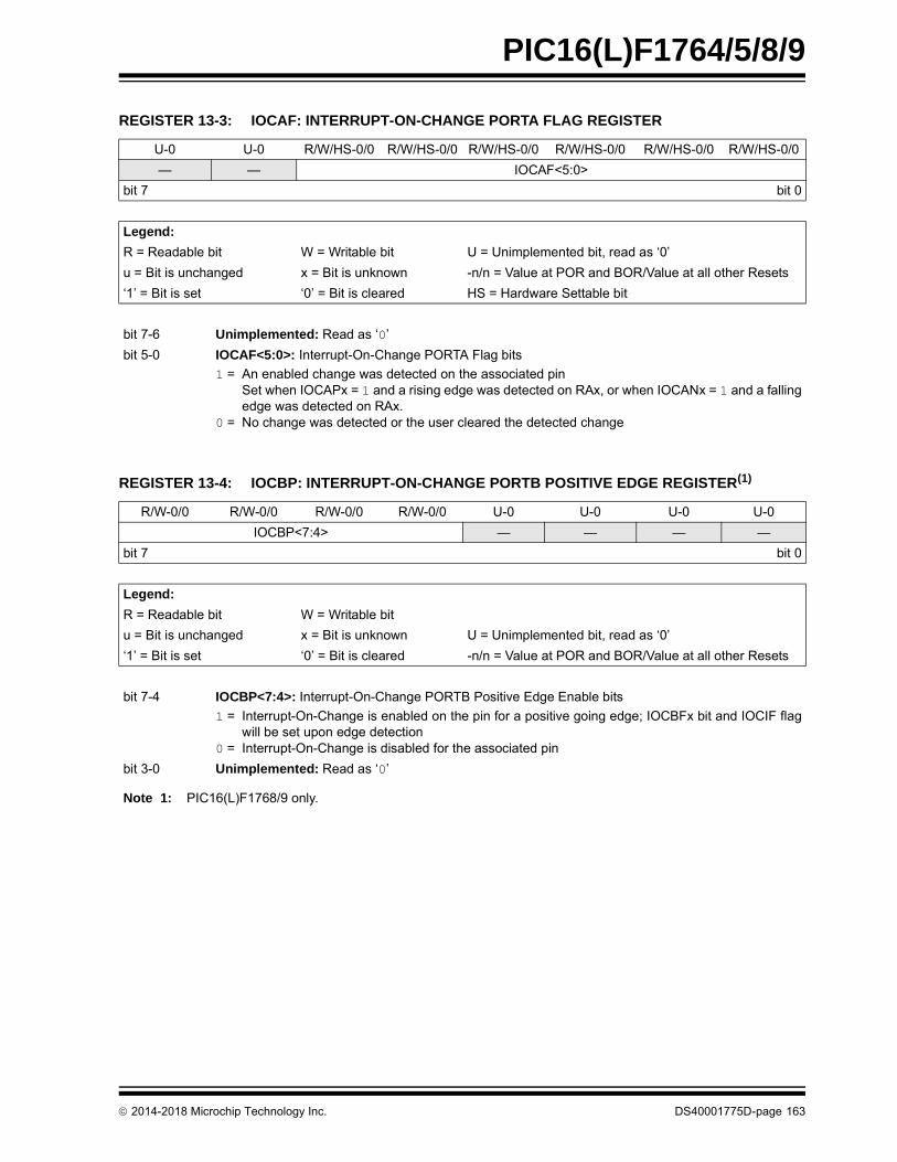
2014-2018 Microchip Technology Inc. DS40001775D-page 163
PIC16(L)F1764/5/8/9
REGISTER 13-3: IOCAF: INTERRUPT-ON-CHANGE PORTA FLAG REGISTER
U-0 U-0 R/W/HS-0/0 R/W/HS-0/0 R/W/HS-0/0 R/W/HS-0/0 R/W/HS-0/0 R/W/HS-0/0
— — IOCAF<5:0>
bit 7 bit 0
Legend:
R = Readable bit W = Writable bit U = Unimplemented bit, read as ‘0’
u = Bit is unchanged x = Bit is unknown -n/n = Value at POR and BOR/Value at all other Resets
‘1’ = Bit is set ‘0’ = Bit is cleared HS = Hardware Settable bit
bit 7-6 Unimplemented: Read as ‘0’
bit 5-0 IOCAF<5:0>: Interrupt-On-Change PORTA Flag bits
1 = An enabled change was detected on the associated pinSet when IOCAPx = 1 and a rising edge was detected on RAx, or when IOCANx = 1 and a fallingedge was detected on RAx.
0 = No change was detected or the user cleared the detected change
REGISTER 13-4: IOCBP: INTERRUPT-ON-CHANGE PORTB POSITIVE EDGE REGISTER(1)
R/W-0/0 R/W-0/0 R/W-0/0 R/W-0/0 U-0 U-0 U-0 U-0
IOCBP<7:4> — — — —
bit 7 bit 0
Legend:
R = Readable bit W = Writable bit
u = Bit is unchanged x = Bit is unknown U = Unimplemented bit, read as ‘0’
‘1’ = Bit is set ‘0’ = Bit is cleared -n/n = Value at POR and BOR/Value at all other Resets
bit 7-4 IOCBP<7:4>: Interrupt-On-Change PORTB Positive Edge Enable bits
1 = Interrupt-On-Change is enabled on the pin for a positive going edge; IOCBFx bit and IOCIF flagwill be set upon edge detection
0 = Interrupt-On-Change is disabled for the associated pin
bit 3-0 Unimplemented: Read as ‘0’
Note 1: PIC16(L)F1768/9 only.

2014-2018 Microchip Technology Inc. DS40001775D-page 164
PIC16(L)F1764/5/8/9
REGISTER 13-5: IOCBN: INTERRUPT-ON-CHANGE PORTB NEGATIVE EDGE REGISTER(1)
R/W-0/0 R/W-0/0 R/W-0/0 R/W-0/0 U-0 U-0 U-0 U-0
IOCBN<7:4> — — — —
bit 7 bit 0
Legend:
R = Readable bit W = Writable bit
u = Bit is unchanged x = Bit is unknown U = Unimplemented bit, read as ‘0’
‘1’ = Bit is set ‘0’ = Bit is cleared -n/n = Value at POR and BOR/Value at all other Resets
bit 7-4 IOCBN<7:4>: Interrupt-On-Change PORTB Negative Edge Enable bits
1 = Interrupt-On-Change is enabled on the pin for a negative going edge; IOCBFx bit and IOCIF flagwill be set upon edge detection
0 = Interrupt-On-Change is disabled for the associated pin
bit 3-0 Unimplemented: Read as ‘0’
Note 1: PIC16(L)F1768/9 only.
REGISTER 13-6: IOCBF: INTERRUPT-ON-CHANGE PORTB FLAG REGISTER(1)
R/W/HS-0/0 R/W/HS-0/0 R/W/HS-0/0 R/W/HS-0/0 U-0 U-0 U-0 U-0
IOCBF<7:4> — — — —
bit 7 bit 0
Legend:
R = Readable bit W = Writable bit U = Unimplemented bit, read as ‘0’
u = Bit is unchanged x = Bit is unknown -n/n = Value at POR and BOR/Value at all other Resets
‘1’ = Bit is set ‘0’ = Bit is cleared HS = Hardware Settable bit
bit 7-4 IOCBF<7:4>: Interrupt-On-Change PORTB Flag bits
1 = An enabled change was detected on the associated pinSet when IOCBPx = 1 and a rising edge was detected on RBx, or when IOCBNx = 1 and a fallingedge was detected on RBx.
0 = No change was detected or the user cleared the detected change
bit 3-0 Unimplemented: Read as ‘0’
Note 1: PIC16(L)F1768/9 only.

2014-2018 Microchip Technology Inc. DS40001775D-page 165
PIC16(L)F1764/5/8/9
REGISTER 13-7: IOCCP: INTERRUPT-ON-CHANGE PORTC POSITIVE EDGE REGISTER
R/W-0/0 R/W-0/0 R/W-0/0 R/W-0/0 R/W-0/0 R/W-0/0 R/W-0/0 R/W-0/0
IOCCP<7:0>(1)
bit 7 bit 0
Legend:
R = Readable bit W = Writable bit
u = Bit is unchanged x = Bit is unknown U = Unimplemented bit, read as ‘0’
‘1’ = Bit is set ‘0’ = Bit is cleared -n/n = Value at POR and BOR/Value at all other Resets
bit 7-0 IOCCP<7:0>: Interrupt-On-Change PORTC Positive Edge Enable bits(1)
1 = Interrupt-On-Change is enabled on the pin for a positive going edge; IOCCFx bit and IOCIF flagwill be set upon edge detection
0 = Interrupt-On-Change is disabled for the associated pin
Note 1: Bits<7:6> are available on PIC16(L)F1768/9 only.
REGISTER 13-8: IOCCN: INTERRUPT-ON-CHANGE PORTC NEGATIVE EDGE REGISTER
R/W-0/0 R/W-0/0 R/W-0/0 R/W-0/0 R/W-0/0 R/W-0/0 R/W-0/0 R/W-0/0
IOCCN<7:0>(1)
bit 7 bit 0
Legend:
R = Readable bit W = Writable bit
u = Bit is unchanged x = Bit is unknown U = Unimplemented bit, read as ‘0’
‘1’ = Bit is set ‘0’ = Bit is cleared -n/n = Value at POR and BOR/Value at all other Resets
bit 7-0 IOCCN<7:0>: Interrupt-On-Change PORTC Negative Edge Enable bits(1)
1 = Interrupt-On-Change is enabled on the pin for a negative going edge; IOCCFx bit and IOCIF flagwill be set upon edge detection
0 = Interrupt-On-Change is disabled for the associated pin
Note 1: Bits<7:6> are available on PIC16(L)F1768/9 only.

2014-2018 Microchip Technology Inc. DS40001775D-page 166
PIC16(L)F1764/5/8/9
TABLE 13-1: SUMMARY OF REGISTERS ASSOCIATED WITH INTERRUPT-ON-CHANGE
REGISTER 13-9: IOCCF: INTERRUPT-ON-CHANGE PORTC FLAG REGISTER
R/W/HS-0/0 R/W/HS-0/0 R/W/HS-0/0 R/W/HS-0/0 R/W/HS-0/0 R/W/HS-0/0 R/W/HS-0/0 R/W/HS-0/0
IOCCF<7:0>(1)
bit 7 bit 0
Legend:
R = Readable bit W = Writable bit U = Unimplemented bit, read as ‘0’
u = Bit is unchanged x = Bit is unknown -n/n = Value at POR and BOR/Value at all other Resets
‘1’ = Bit is set ‘0’ = Bit is cleared HS = Hardware Settable bit
bit 7-0 IOCCF<7:0>: Interrupt-On-Change PORTC Flag bits(1)
1 = An enabled change was detected on the associated pinSet when IOCCPx = 1 and a rising edge was detected on RCx, or when IOCCNx = 1 and a fallingedge was detected on RCx
0 = No change was detected or the user cleared the detected change
Note 1: Bits<7:6> are available on PIC16(L)F1768/9 only.
Name Bit 7 Bit 6 Bit 5 Bit 4 Bit 3 Bit 2 Bit 1 Bit 0Register on Page
ANSELA — — — ANSA4 — ANSA<2:0> 137
ANSELB(1) ANSB<7:4> — — — — 143
ANSELC ANSC<7:6>(1) — — ANSC<3:0> 148
INTCON GIE PEIE TMR0IE INTE IOCIE TMR0IF INTF IOCIF 101
IOCAF — — IOCAF<5:0> 163
IOCAN — — IOCAN<5:0> 162
IOCAP — — IOCAP<5:0> 162
IOCBF(1) IOCBF<7:4> — — — — 164
IOCBN(1) IOCBN<7:4> — — — — 164
IOCBP(1) IOCBP<7:4> — — — — 163
IOCCF IOCCF<7:6>(1) IOCCF<5:0> 166
IOCCN IOCCN<7:6>(1) IOCCN<5:0> 165
IOCCP IOCCP<7:6>(1) IOCCP<5:0> 165
TRISA — — TRISA<5:4> —(2) TRISA<2:0> 136
TRISB(1) TRISB<7:4> — — — — 142
TRISC TRISC<7:6>(1) TRISC<5:0> 147
Legend: — = unimplemented location, read as ‘0’. Shaded cells are not used by Interrupt-On-Change.
Note 1: PIC16(L)F1768/9 only.
2: Unimplemented, read as ‘1’.

2014-2018 Microchip Technology Inc. DS40001775D-page 167
PIC16(L)F1764/5/8/9
14.0 FIXED VOLTAGE REFERENCE (FVR)
The Fixed Voltage Reference, or FVR, is a stablevoltage reference, independent of VDD, with 1.024V,2.048V or 4.096V selectable output levels. The outputof the FVR can be configured to supply a referencevoltage to the following:
• ADC input channel
• ADC positive reference
• Comparator positive input
• Digital-to-Analog Converter (DAC)
The FVR can be enabled by setting the FVREN bit ofthe FVRCON register.
14.1 Independent Gain Amplifiers
The output of the FVR supplied to the ADC,Comparators and DAC is routed through twoindependent Programmable Gain Amplifiers (PGAs).Each amplifier can be programmed for a gain of 1x, 2xor 4x, to produce the three possible voltage levels.
The ADFVR<1:0> bits of the FVRCON register are usedto enable and configure the gain amplifier settings for thereference supplied to the ADC module. ReferenceSection 16.0 “Analog-to-Digital Converter (ADC)Module” for additional information.
The CDAFVR<1:0> bits of the FVRCON register are usedto enable and configure the gain amplifier settings for thereference supplied to the DAC and comparator module.Reference Section 17.0 “5-Bit Digital-to-Analog Con-verter (DAC) Module” and Section 19.0 “ComparatorModule” for additional information.
14.2 FVR Stabilization Period
When the Fixed Voltage Reference module is enabled, itrequires time for the reference and amplifier circuits tostabilize. Once the circuits stabilize and are ready foruse, the FVRRDY bit of the FVRCON register will beset. See Figure 37-76 in Section 37.0 “DC and ACCharacteristics Graphs and Charts”.
14.3 FVR Buffer Stabilization Period
When either FVR Buffer1 or Buffer2 is enabled, thenthe buffer amplifier circuits require 30 s to stabilize.This stabilization time is required even when the FVRis already operating and stable.

2014-2018 Microchip Technology Inc. DS40001775D-page 168
PIC16(L)F1764/5/8/9
FIGURE 14-1: VOLTAGE REFERENCE BLOCK DIAGRAM
ADFVR<1:0>
CDAFVR<1:0>
X1X2X4
2
2
FVR Buffer1(To ADC Module)
FVR Buffer2(To Comparators, DAC)
FVREN FVRRDY
Any Peripheral Requiring the Fixed Reference
(see Table 14-1)
To BOR, LDO
HFINTOSC Enable
HFINTOSC
+
_
X1X2X4
TABLE 14-1: PERIPHERALS REQUIRING THE FIXED VOLTAGE REFERENCE (FVR)
Peripheral Conditions Description
HFINTOSC FOSC<2:0> = 100 and IRCF<3:0> 000x
INTOSC is active and device is not in Sleep
BOR BOREN<1:0> = 11 BOR is always enabled
BOREN<1:0> = 10 and BORFS = 1 BOR is disabled in Sleep mode, BOR fast start is enabled
BOREN<1:0> = 01 and BORFS = 1 BOR under software control, BOR fast start is enabled
LDO All PIC16F1764/5/8/9 devices when VREGPM = 1 and not in Sleep
The device runs off of the ULP regulator when in Sleep mode

2014-2018 Microchip Technology Inc. DS40001775D-page 169
PIC16(L)F1764/5/8/9
14.4 Register Definitions: FVR Control
TABLE 14-2: SUMMARY OF REGISTERS ASSOCIATED WITH FIXED VOLTAGE REFERENCE
REGISTER 14-1: FVRCON: FIXED VOLTAGE REFERENCE CONTROL REGISTER
R/W-0/0 R-q/q R/W-0/0 R/W-0/0 R/W-0/0 R/W-0/0 R/W-0/0 R/W-0/0
FVREN FVRRDY(1) TSEN(3) TSRNG(3) CDAFVR<1:0> ADFVR<1:0>
bit 7 bit 0
Legend:
R = Readable bit W = Writable bit U = Unimplemented bit, read as ‘0’
u = Bit is unchanged x = Bit is unknown -n/n = Value at POR and BOR/Value at all other Resets
‘1’ = Bit is set ‘0’ = Bit is cleared q = Value depends on condition
bit 7 FVREN: Fixed Voltage Reference Enable bit
1 = Fixed Voltage Reference is enabled0 = Fixed Voltage Reference is disabled
bit 6 FVRRDY: Fixed Voltage Reference Ready Flag bit(1)
1 = Fixed Voltage Reference output is ready for use0 = Fixed Voltage Reference output is not ready or not enabled
bit 5 TSEN: Temperature Indicator Enable bit(3)
1 = Temperature indicator is enabled0 = Temperature indicator is disabled
bit 4 TSRNG: Temperature Indicator Range Selection bit(3)
1 = VOUT = VDD – 4 VT (High Range)0 = VOUT = VDD – 2 VT (Low Range)
bit 3-2 CDAFVR<1:0>: Comparator/DAC FVR Buffer Gain Selection bits
11 = Comparator/DAC FVR buffer gain is 4x with output, VCDAFVR = 4x VFVR(2)
10 = Comparator/DAC FVR buffer gain is 2x with output, VCDAFVR = 2x VFVR(2)
01 = Comparator/DAC FVR buffer gain is 1x with output, VCDAFVR = 1x VFVR
00 = Comparator/DAC FVR buffer is off
bit 1-0 ADFVR<1:0>: ADC FVR Buffer Gain Selection bits
11 = ADC FVR buffer gain is 4x with output, VADFVR = 4x VFVR(2)
10 = ADC FVR buffer gain is 2x with output, VADFVR = 2x VFVR(2)
01 = ADC FVR buffer gain is 1x with output, VADFVR = 1x VFVR
00 = ADC FVR buffer is off
Note 1: FVRRDY is always ‘1’ on PIC16F1764/5/8/9 only.2: Fixed Voltage Reference output cannot exceed VDD.
3: See Section 15.0 “Temperature Indicator Module” for additional information.
Name Bit 7 Bit 6 Bit 5 Bit 4 Bit 3 Bit 2 Bit 1 Bit 0Register on Page
FVRCON FVREN FVRRDY TSEN TSRNG CDAFVR<1:0> ADFVR<1:0> 169

2014-2018 Microchip Technology Inc. DS40001775D-page 170
PIC16(L)F1764/5/8/9
15.0 TEMPERATURE INDICATOR MODULE
This family of devices is equipped with a temperaturecircuit designed to measure the operating temperatureof the silicon die. The circuit’s range of operatingtemperature falls between -40°C and +85°C. Theoutput is a voltage that is proportional to the devicetemperature. The output of the temperature indicator isinternally connected to the device ADC.
The circuit may be used as a temperature thresholddetector or a more accurate temperature indicator,depending on the level of calibration performed. A one-point calibration allows the circuit to indicate atemperature closely surrounding that point. A two-pointcalibration allows the circuit to sense the entire rangeof temperature more accurately. Reference ApplicationNote AN1333, “Use and Calibration of the InternalTemperature Indicator” (DS00001333) for more detailsregarding the calibration process.
15.1 Circuit Operation
Figure 15-1 shows a simplified block diagram of thetemperature circuit. The proportional voltage output isachieved by measuring the forward voltage drop acrossmultiple silicon junctions.
Equation 15-1 describes the output characteristics ofthe temperature indicator.
EQUATION 15-1: VOUT RANGES
The temperature sense circuit is integrated with theFixed Voltage Reference (FVR) module. SeeSection 14.0 “Fixed Voltage Reference (FVR)” formore information.
The circuit is enabled by setting the TSEN bit of theFVRCON register. When disabled, the circuit draws nocurrent.
The circuit operates in either high or low range. The highrange, selected by setting the TSRNG bit of theFVRCON register, provides a wider output voltage. Thisprovides more resolution over the temperature range,but may be less consistent from part to part. This rangerequires a higher bias voltage to operate and thus, ahigher VDD is needed.
The low range is selected by clearing the TSRNG bitof the FVRCON register. The low range generates alower voltage drop and thus, a lower bias voltage isneeded to operate the circuit. The low range isprovided for low-voltage operation.
FIGURE 15-1: TEMPERATURE CIRCUIT DIAGRAM
15.2 Minimum Operating VDD
When the temperature circuit is operated in low range,the device may be operated at any operating voltagethat is within specifications.
When the temperature circuit is operated in high range,the device operating voltage, VDD, must be highenough to ensure that the temperature circuit iscorrectly biased.
Table 15-1 shows the recommended minimum VDD vs.range setting.
TABLE 15-1: RECOMMENDED VDD VS. RANGE
High Range: VOUT = VDD – 4VT
Low Range: VOUT = VDD – 2VT
Min. VDD, TSRNG = 1 Min. VDD, TSRNG = 0
3.6V 1.8V
VOUT
Temp. IndicatorTo ADC
TSRNG
TSEN
Rev. 10-000069A7/31/2013VDD

2014-2018 Microchip Technology Inc. DS40001775D-page 171
PIC16(L)F1764/5/8/9
15.3 Temperature Output
The output of the circuit is measured using the internalAnalog-to-Digital Converter. A channel is reserved forthe temperature circuit output. Refer to Section 16.0“Analog-to-Digital Converter (ADC) Module” fordetailed information.
15.4 ADC Acquisition Time
To ensure accurate temperature measurements, theuser must wait at least 200 s after the ADC inputmultiplexer is connected to the temperature indicatoroutput before the conversion is performed. In addition,the user must wait 200 s between sequentialconversions of the temperature indicator output.
TABLE 15-2: SUMMARY OF REGISTERS ASSOCIATED WITH THE TEMPERATURE INDICATOR
Name Bit 7 Bit 6 Bit 5 Bit 4 Bit 3 Bit 2 Bit 1 Bit 0Register on Page
FVRCON FVREN FVRRDY TSEN TSRNG CDFVR<1:0> ADFVR<1:0> 169
Legend: Shaded cells are unused by the temperature indicator module.

2014-2018 Microchip Technology Inc. DS40001775D-page 172
PIC16(L)F1764/5/8/9
16.0 ANALOG-TO-DIGITAL CONVERTER (ADC) MODULE
The Analog-to-Digital Converter (ADC) allowsconversion of an analog input signal to a 10-bit binaryrepresentation of that signal. This device uses analoginputs, which are multiplexed into a singleSample-and-Hold (S&H) circuit. The output of theSample-and-Hold is connected to the input of the con-verter. The converter generates a 10-bit binary result viasuccessive approximation and stores the conversionresult into the ADC Result registers (ADRESH:ADRESLregister pair). Figure 16-1 shows the block diagram ofthe ADC.
The ADC voltage reference is software-selectable to beeither internally generated or externally supplied.
The ADC can generate an interrupt upon completion ofa conversion. This interrupt can be used to wake-up thedevice from Sleep.
FIGURE 16-1: ADC BLOCK DIAGRAM
VDD
VREF+ ADPREF<1:0> = 10
ADPREF<1:0> = 00
FVR_buffer1
Note 1: When ADON = 0, all multiplexer inputs are disconnected.
2: PIC16(L)F1768/9 only
ADON(1)
GO/DONE
VSS
ADC
00000
00001
00010
00011
00100
00101
00111
00110
01000
01001
01010
01011
CHS<4:0>
AN0
VREF+/AN1
AN2
AN4
AN5
AN6
AN7
AN3
AN8(2)
AN9(2)
AN10(2)
AN11(2)
11111
ADRESH ADRESL
10
16
ADFM0 = Left Justify1 = Right Justify
Temp Indicator 11101
DAC1_output 11110
VSS
Ref- Ref+
11100
VREF- ADNREF = 1
ADNREF = 0
DAC2_output(2)
DAC3_output
DAC4_output(2)
11011
11010
ADPREF<1:0> = 11FVR_buffer1

2014-2018 Microchip Technology Inc. DS40001775D-page 173
PIC16(L)F1764/5/8/9
16.1 ADC Configuration
When configuring and using the ADC the followingfunctions must be considered:
• Port configuration• Channel selection• ADC voltage reference selection• ADC conversion clock source• Interrupt control• Result formatting
16.1.1 PORT CONFIGURATION
The ADC can be used to convert both analog anddigital signals. When converting analog signals, the I/Opin should be configured for analog by setting theassociated TRISx and ANSELx bits. Refer toSection 11.0 “I/O Ports” for more information.
16.1.2 CHANNEL SELECTION
There are up to 18 channel selections available:
• AN<7:0> pins• AN<11:8> pins (PIC16(L)F1768/9 only)• Temperature indicator• DAC1_output and DAC3_output• DAC2_output and DAC4_output
(PIC16(L)F1768/9 only)• FVR_buffer1
The CHS<4:0> bits of the ADCON0 register(Register 16-1) determine which channel is connectedto the Sample-and-Hold circuit.
When changing channels, a delay is required beforestarting the next conversion. Refer to Section 16.2“ADC Operation” for more information.
16.1.3 ADC POSITIVE VOLTAGE REFERENCE
The ADPREF<1:0> bits of the ADCON1 registerprovide control of the positive voltage reference. Thepositive voltage reference can be:
• VREF+ pin
• VDD
• FVR 2.048V
• FVR 4.096V (not available on LF devices)
• VSS
See Section 16.0 “Analog-to-Digital Converter(ADC) Module” for more details on the Fixed VoltageReference.
16.1.4 ADC NEGATIVE VOLTAGE REFERENCE
The ADNREF bit of the ADCON1 register providescontrol of the negative voltage reference. The negativevoltage reference can be:
• VREF- pin
• VSS
16.1.5 CONVERSION CLOCK
The source of the conversion clock is software-selectablevia the ADCS<2:0> bits of the ADCON1 register. Thereare seven possible clock options:
• FOSC/2
• FOSC/4
• FOSC/8
• FOSC/16
• FOSC/32
• FOSC/64
• FRC (internal RC oscillator)
The time to complete one bit conversion is defined asTAD. One full 10-bit conversion requires 11.5 TAD
periods, as shown in Figure 16-2.
For correct conversion, the appropriate TAD specificationmust be met. Refer to Table 36-16: ADC ConversionRequirements for more information. Table 16-1 givesexamples of appropriate ADC clock selections.
Note: Analog voltages on any pin that is definedas a digital input may cause the inputbuffer to conduct excess current.
Note: It is recommended that when switchingfrom an ADC channel of a higher voltageto a channel of a lower voltage, that theuser selects the VSS channel before con-necting to the channel with the lower volt-age. If the ADC does not have a dedicatedVSS input channel, the VSS selection(DAC1R<4:0> = b'00000') through theDAC output channel can be used. If theDAC is in use, a free input channel can beconnected to VSS, and can be used inplace of the DAC.
Note: Unless using the FRC, any changes in thesystem clock frequency will change theADC clock frequency, which mayadversely affect the ADC result.

2014-2018 Microchip Technology Inc. DS40001775D-page 174
PIC16(L)F1764/5/8/9
TABLE 16-1: ADC CLOCK PERIOD (TAD) VS. DEVICE OPERATING FREQUENCIES
FIGURE 16-2: ANALOG-TO-DIGITAL CONVERSION TAD CYCLES
ADC Clock Period (TAD) Device Frequency (FOSC)
ADC Clock Source
ADCS<2:0> 32 MHz 20 MHz 16 MHz 8 MHz 4 MHz 1 MHz
FOSC/2 000 62.5ns(2) 100 ns(2) 125 ns(2) 250 ns(2) 500 ns(2) 2.0 s
FOSC/4 100 125 ns(2) 200 ns(2) 250 ns(2) 500 ns(2) 1.0 s 4.0 s
FOSC/8 001 0.5 s(2) 400 ns(2) 0.5 s(2) 1.0 s 2.0 s 8.0 s(3)
FOSC/16 101 800 ns 800 ns 1.0 s 2.0 s 4.0 s 16.0 s(2)
FOSC/32 010 1.0 s 1.6 s 2.0 s 4.0 s 8.0 s(3) 32.0 s(2)
FOSC/64 110 2.0 s 3.2 s 4.0 s 8.0 s(3) 16.0 s(2) 64.0 s(2)
FRC x11 1.0-6.0 s(1,4) 1.0-6.0 s(1,4) 1.0-6.0 s(1,4) 1.0-6.0 s(1,4) 1.0-6.0 s(1,4) 1.0-6.0 s(1,4)
Legend: Shaded cells are outside of the recommended range.
Note 1: See the TAD parameter for FRC source typical TAD value.
2: These values violate the required TAD time.
3: Outside the recommended TAD time.
4: The ADC clock period (TAD) and total ADC conversion time can be minimized when the ADC clock is derived from the system clock, FOSC. However, the FRC oscillator source must be used when conversions are to be performed with the device in Sleep mode.
TAD1 TAD2 TAD3 TAD4 TAD5 TAD6 TAD7 TAD8 TAD9 TAD10 TAD11
Set GO bit
Conversion Starts
Holding capacitor disconnectedfrom analog input (THCD).
On the following cycle:
ADRESH:ADRESL is loaded,GO bit is cleared,
ADIF bit is set,holding capacitor is reconnected to analog input.
b9 b8 b7 b6 b5 b4 b3 b2 b1 b0
Enable ADC (ADON bit)and
Select channel (ACS bits)
THCD
TACQ
Rev. 10-000035A7/30/2013

2014-2018 Microchip Technology Inc. DS40001775D-page 175
PIC16(L)F1764/5/8/9
16.1.6 INTERRUPTS
The ADC module allows for the ability to generate aninterrupt upon completion of an Analog-to-Digitalconversion. The ADC Interrupt Flag is the ADIF bit inthe PIR1 register. The ADC Interrupt Enable bit is theADIE bit in the PIE1 register. The ADIF bit must becleared in software.
This interrupt can be generated while the device isoperating or while in Sleep. If the device is in Sleep, theinterrupt will wake-up the device. Upon waking fromSleep, the next instruction following the SLEEPinstruction is always executed. If the user is attemptingto wake-up from Sleep and resume in-line codeexecution, the ADIE bit of the PIE1 register and thePEIE bit of the INTCON register must both be set, andthe GIE bit of the INTCON register must be cleared. Ifall three of these bits are set, the execution will switchto the Interrupt Service Routine.
16.1.7 RESULT FORMATTING
The 10-bit ADC conversion result can be supplied intwo formats, left justified or right justified. The ADFM bitof the ADCON1 register controls the output format.
Figure 16-3 shows the two output formats.
FIGURE 16-3: 10-BIT ADC CONVERSION RESULT FORMAT
Note 1: The ADIF bit is set at the completion ofevery conversion, regardless of whetheror not the ADC interrupt is enabled.
2: The ADC operates during Sleep onlywhen the FRC oscillator is selected.
MSb
MSb
LSb
LSb
(ADFM = 0)
(ADFM = 1)
bit 7 bit 7
bit 7bit 7
bit 0
bit 0
bit 0
bit 0
10-bit ADC Result
10-bit ADC ResultUnimplemented: Read as ‘0’
Unimplemented: Read as ‘0’
ADRESH ADRESL
Rev. 10-000 054A12/21/201 6

2014-2018 Microchip Technology Inc. DS40001775D-page 176
PIC16(L)F1764/5/8/9
16.2 ADC Operation
16.2.1 STARTING A CONVERSION
To enable the ADC module, the ADON bit of theADCON0 register must be set to a ‘1’. Setting theGO/DONE bit of the ADCON0 register to a ‘1’ will startthe Analog-to-Digital conversion.
16.2.2 COMPLETION OF A CONVERSION
When the conversion is complete, the ADC module will:
• Clear the GO/DONE bit • Set the ADIF interrupt flag bit• Update the ADRESH and ADRESL registers with
the new conversion result
16.2.3 TERMINATING A CONVERSION
If a conversion must be terminated before completion,the GO/DONE bit can be cleared in software. TheADRESH and ADRESL registers will be updated withthe partially complete Analog-to-Digital conversionsample. Incomplete bits will match the last bitconverted.
16.2.4 ADC OPERATION DURING SLEEP
The ADC module can operate during Sleep. Thisrequires the ADC clock source to be set to the FRCoption. When the FRC oscillator source is selected, theADC waits one additional instruction before starting theconversion. This allows the SLEEP instruction to beexecuted, which can reduce system noise during theconversion. If the ADC interrupt is enabled, the devicewill wake-up from Sleep when the conversioncompletes. If the ADC interrupt is disabled, the ADCmodule is turned off after the conversion completes,although the ADON bit remains set.
When the ADC clock source is something other thanFRC, a SLEEP instruction causes the present conver-sion to be aborted and the ADC module is turned off,although the ADON bit remains set.
16.2.5 AUTO-CONVERSION TRIGGER
The auto-conversion trigger allows periodic ADCmeasurements without software intervention. When arising edge of the selected source occurs, theGO/DONE bit is set by hardware.
The auto-conversion trigger source is selected with theTRIGSEL<4:0> bits of the ADCON2 register.
Using the auto-conversion trigger does not assureproper ADC timing. It is the user’s responsibility toensure that the ADC timing requirements are met.
See Table 16-2 for auto-conversion sources.
Note: The GO/DONE bit should not be set in thesame instruction that turns on the ADC.Refer to Section 16.2.6 “ADC ConversionProcedure”.
Note: A device Reset forces all registers to theirReset state. Thus, the ADC module isturned off and any pending conversion isterminated.
TABLE 16-2: AUTO-CONVERSION SOURCES
Source Peripheral Signal Name
CCP1 CCP1_trigger
CCP2(1) CCP2_trigger
Timer0 T0_overflow
Timer1 T1_overflow
Timer3 T3_overflow
Timer5 T5_overflow
Timer2 T2_postscaled
Timer4 T4_postscaled
Timer6 T6_postscaled
Comparator C1 sync_C1OUT
Comparator C2 sync_C2OUT
Comparator C3(1) sync_C3OUT
Comparator C4(1) sync_C4OUT
CLC1 LC1_out
CLC2 LC2_out
CLC3 LC3_out
PWM3 PWM3OUT
PWM4(1) PWM4OUT
PWM5 PR/PH/OF/DC5_match
PWM6(1) PR/PH/OF/DC6_match
Note 1: PIC16(L)F1768/9 only

2014-2018 Microchip Technology Inc. DS40001775D-page 177
PIC16(L)F1764/5/8/9
16.2.6 ADC CONVERSION PROCEDURE
This is an example procedure for using the ADC toperform an Analog-to-Digital conversion:
1. Configure the PORT:
• Disable the pin output driver (refer to the TRISx register)
• Configure pin as an analog (refer to the ANSELx register)
• Disable weak pull-ups either globally (Refer to the OPTION_REG register) or individually (Refer to the appropriate WPUx register)
2. Configure the ADC module:
• Select ADC conversion clock
• Configure voltage reference
• Select ADC input channel
• Turn on ADC module
3. Configure ADC interrupt (optional):
• Clear ADC interrupt flag
• Enable ADC interrupt
• Enable peripheral interrupt
• Enable global interrupt(1)
4. Wait the required acquisition time.(2)
5. Start conversion by setting the GO/DONE bit.
6. Wait for ADC conversion to complete by one ofthe following:
• Polling the GO/DONE bit
• Waiting for the ADC interrupt (interrupts enabled)
7. Read ADC result.
8. Clear the ADC interrupt flag (required if interruptis enabled).
EXAMPLE 16-1: ADC CONVERSION
Note 1: The global interrupt can be disabled if theuser is attempting to wake-up from Sleepand resume in-line code execution.
2: Refer to Section 16.4 “ADC AcquisitionRequirements”.
;This code block configures the ADC;for polling, Vdd and Vss references, FRC ;oscillator and AN0 input.;;Conversion start & polling for completion ; are included.;BANKSEL ADCON1 ;MOVLW B’11110000’ ;Right justify, FRC
;oscillatorMOVWF ADCON1 ;Vdd and Vss VrefBANKSEL TRISA ;BSF TRISA,0 ;Set RA0 to inputBANKSEL ANSEL ;BSF ANSEL,0 ;Set RA0 to analogBANKSEL WPUABCF WPUA,0 ;Disable weak
;pull-up on RA0BANKSEL ADCON0 ;MOVLW B’00000001’ ;Select channel AN0MOVWF ADCON0 ;Turn ADC OnCALL SampleTime ;Acquisiton delayBSF ADCON0,ADGO ;Start conversionBTFSC ADCON0,ADGO ;Is conversion done?GOTO $-1 ;No, test againBANKSEL ADRESH ;MOVF ADRESH,W ;Read upper 2 bitsMOVWF RESULTHI ;store in GPR spaceBANKSEL ADRESL ;MOVF ADRESL,W ;Read lower 8 bitsMOVWF RESULTLO ;Store in GPR space

2014-2018 Microchip Technology Inc. DS40001775D-page 178
PIC16(L)F1764/5/8/9
16.3 Register Definitions: ADC Control
REGISTER 16-1: ADCON0: ADC CONTROL REGISTER 0
U-0 R/W-0/0 R/W-0/0 R/W-0/0 R/W-0/0 R/W-0/0 R/W-0/0 R/W-0/0
— CHS<4:0> GO/DONE ADON
bit 7 bit 0
Legend:
R = Readable bit W = Writable bit
u = Bit is unchanged x = Bit is unknown U = Unimplemented bit, read as ‘0’
‘1’ = Bit is set ‘0’ = Bit is cleared -n/n = Value at POR and BOR/Value at all other Resets
bit 7 Unimplemented: Read as ‘0’
bit 6-2 CHS<4:0>: Analog Channel Select bits
11111 = FVR (Fixed Voltage Reference) Buffer1 Output(2)
11110 = DAC1_output(1)
11101 = Temperature indicator(3)
11100 = DAC2_output(1,5)
11011 = DAC3_output(4)
11010 = DAC4_output(4,5)
11001 = Reserved; no channel connected • • •01111 = Switched AN7(5,6)
01110 = Switched AN6(6)
01101 = Reserved; no channel connected.01100 = Reserved; no channel connected.01011 = AN11(5)
01010 = AN10(5)
01001 = AN9(5)
01000 = AN8(5)
00111 = AN700110 = AN600101 = AN500100 = AN400011 = AN300010 = AN200001 = AN100000 = AN0
bit 1 GO/DONE: ADC Conversion Status bit
1 = ADC conversion cycle in progress; setting this bit starts an ADC conversion cycleThis bit is automatically cleared by hardware when the ADC conversion has completed.
0 = ADC conversion completed/not in progress
bit 0 ADON: ADC Enable bit
1 = ADC is enabled0 = ADC is disabled and consumes no operating current
Note 1: See Section 17.0 “5-Bit Digital-to-Analog Converter (DAC) Module” for more information.2: See Section 14.0 “Fixed Voltage Reference (FVR)” for more information.3: See Section 15.0 “Temperature Indicator Module” for more information.
4: See Section 18.0 “10-Bit Digital-to-Analog Converter (DAC) Module” for more information.
5: PIC16(L)F1768/9 only.
6: Input source is switched off when op amp override is forced tri-state. See Section 29.3 “Override Control”.

2014-2018 Microchip Technology Inc. DS40001775D-page 179
PIC16(L)F1764/5/8/9
REGISTER 16-2: ADCON1: ADC CONTROL REGISTER 1
R/W-0/0 R/W-0/0 R/W-0/0 R/W-0/0 U-0 R/W-0/0 R/W-0/0 R/W-0/0
ADFM ADCS<2:0> — ADNREF ADPREF<1:0>
bit 7 bit 0
Legend:
R = Readable bit W = Writable bit
u = Bit is unchanged x = Bit is unknown U = Unimplemented bit, read as ‘0’
‘1’ = Bit is set ‘0’ = Bit is cleared -n/n = Value at POR and BOR/Value at all other Resets
bit 7 ADFM: ADC Result Format Select bit
1 = Right justified; six Most Significant bits of ADRESH are set to ‘0’ when the conversion result isloaded
0 = Left justified; six Least Significant bits of ADRESL are set to ‘0’ when the conversion result isloaded
bit 6-4 ADCS<2:0>: ADC Conversion Clock Select bits
111 = FRC (clock supplied from an internal RC oscillator)110 = FOSC/64101 = FOSC/16100 = FOSC/4011 = FRC (clock supplied from an internal RC oscillator)010 = FOSC/32001 = FOSC/8000 = FOSC/2
bit 3 Unimplemented: Read as ‘0’
bit 2 ADNREF: ADC Negative Voltage Reference Configuration bit
1 =VREF- is connected to external VREF- pin0 =VREF- is connected to VSS
bit 1-0 ADPREF<1:0>: ADC Positive Voltage Reference Configuration bits
11 = VREF+ is connected to the internal Fixed Voltage Reference (FVR) module(1)
10 = VREF+ is connected to the external VREF+ pin(1)
01 = Reserved00 = VREF+ is connected to VDD
Note 1: When selecting the VREF+ pin as the source of the positive reference, be aware that a minimum voltage specification exists. See Table 36-16 for details.

2014-2018 Microchip Technology Inc. DS40001775D-page 180
PIC16(L)F1764/5/8/9
REGISTER 16-3: ADCON2: ADC CONTROL REGISTER 2
R/W-0/0 R/W-0/0 R/W-0/0 R/W-0/0 R/W-0/0 U-0 U-0 U-0
TRIGSEL<4:0>(1) — — —
bit 7 bit 0
Legend:
R = Readable bit W = Writable bit U = Unimplemented bit, read as ‘0’
u = Bit is unchanged x = Bit is unknown -n/n = Value at POR and BOR/Value at all other Resets
‘1’ = Bit is set ‘0’ = Bit is cleared
bit 7-3 TRIGSEL<4:0>: Auto-Conversion Trigger Selection bits(1)
11111 = Reserved • • •11011 = Reserved11010 = PWM6 – OF6_match(2)
11001 = PWM6 – PH6_match(2)
11000 = PWM6 – PR6_match(2)
10111 = PWM6 – DC6_match(2)
10110 = PWM5 – OF5_match10101 = PWM5 – PH5_match10100 = PWM5 – PR5_match10011 = PWM5 – DC5_match10010 = PWM4 – PWM4OUT(2)
10001 = PWM3 – PWM3OUT10000 = CCP2 – CCP2_trigger(2)
01111 = CCP1 – CCP1_trigger01110 = CLC3 – LC3_out01101 = CLC2 – LC2_out01100 = CLC1 – LC1_out01011 = Comparator C4 – sync_C4OUT(2)
01010 = Comparator C3 – sync_C3OUT(2)
01001 = Comparator C2 – sync_C2OUT01000 = Comparator C1 – sync_C1OUT00111 = Timer6 – T6_postscaled00110 = Timer5 – T5_overflow00101 = Timer4 – T4_postscaled00100 = Timer3 – T3_overflow00011 = Timer2 – T2_postscaled00010 = Timer1 – T1_overflow00001 = Timer0 – T0_overflow00000 = No auto-conversion trigger selected
bit 3-0 Unimplemented: Read as ‘0’
Note 1: This is a rising edge-sensitive input for all sources.
2: PIC16(L)F1768/9 only; reserved otherwise.

2014-2018 Microchip Technology Inc. DS40001775D-page 181
PIC16(L)F1764/5/8/9
REGISTER 16-4: ADRESH: ADC RESULT REGISTER HIGH (ADFM = 0)
R/W-x/u R/W-x/u R/W-x/u R/W-x/u R/W-x/u R/W-x/u R/W-x/u R/W-x/u
ADRES<9:2>
bit 7 bit 0
Legend:
R = Readable bit W = Writable bit
u = Bit is unchanged x = Bit is unknown U = Unimplemented bit, read as ‘0’
‘1’ = Bit is set ‘0’ = Bit is cleared -n/n = Value at POR and BOR/Value at all other Resets
bit 7-0 ADRES<9:2>: ADC Result Register bits
Upper eight bits of 10-bit conversion result.
REGISTER 16-5: ADRESL: ADC RESULT REGISTER LOW (ADFM = 0)
R/W-x/u R/W-x/u r-x/u r-x/u r-x/u r-x/u r-x/u r-x/u
ADRES<1:0> — — — — — —
bit 7 bit 0
Legend:
R = Readable bit W = Writable bit r = Reserved bit
u = Bit is unchanged x = Bit is unknown U = Unimplemented bit, read as ‘0’
‘1’ = Bit is set ‘0’ = Bit is cleared -n/n = Value at POR and BOR/Value at all other Resets
bit 7-6 ADRES<1:0>: ADC Result Register bits
Lower two bits of 10-bit conversion result.
bit 5-0 Reserved: Do not use.

2014-2018 Microchip Technology Inc. DS40001775D-page 182
PIC16(L)F1764/5/8/9
REGISTER 16-6: ADRESH: ADC RESULT REGISTER HIGH (ADFM = 1)
r-x/u r-x/u r-x/u r-x/u r-x/u r-x/u R/W-x/u R/W-x/u
— — — — — — ADRES<9:8>
bit 7 bit 0
Legend:
R = Readable bit W = Writable bit r = Reserved bit
u = Bit is unchanged x = Bit is unknown U = Unimplemented bit, read as ‘0’
‘1’ = Bit is set ‘0’ = Bit is cleared -n/n = Value at POR and BOR/Value at all other Resets
bit 7-2 Reserved: Do not use.
bit 1-0 ADRES<9:8>: ADC Result Register bits
Upper two bits of 10-bit conversion result.
REGISTER 16-7: ADRESL: ADC RESULT REGISTER LOW (ADFM = 1)
R/W-x/u R/W-x/u R/W-x/u R/W-x/u R/W-x/u R/W-x/u R/W-x/u R/W-x/u
ADRES<7:0>
bit 7 bit 0
Legend:
R = Readable bit W = Writable bit
u = Bit is unchanged x = Bit is unknown U = Unimplemented bit, read as ‘0’
‘1’ = Bit is set ‘0’ = Bit is cleared -n/n = Value at POR and BOR/Value at all other Resets
bit 7-0 ADRES<7:0>: ADC Result Register bits
Lower eight bits of 10-bit conversion result.

2014-2018 Microchip Technology Inc. DS40001775D-page 183
PIC16(L)F1764/5/8/9
16.4 ADC Acquisition Requirements
For the ADC to meet its specified accuracy, the ChargeHolding Capacitor (CHOLD) must be allowed to fullycharge to the input channel voltage level. The analoginput model is shown in Figure 16-4. The SourceImpedance (RS) and the internal Sampling Switch(RSS) impedance directly affect the time required tocharge the capacitor, CHOLD. The Sampling Switch(RSS) impedance varies over the device voltage (VDD),refer to Figure 16-4. The maximum recommendedimpedance for analog sources is 10 k. As the
source impedance is decreased, the acquisition timemay be decreased. After the analog input channel isselected (or changed), an ADC acquisition must bedone before the conversion can be started. To calculatethe minimum acquisition time, Equation 16-1 may beused. This equation assumes that 1/2 LSb error is used(1,024 steps for the ADC). The 1/2 LSb error is themaximum error allowed for the ADC to meet itsspecified resolution.
EQUATION 16-1: ACQUISITION TIME EXAMPLE
TACQ Amplifier Settling Time Hold Capacitor Charging Time Temperature Coefficient+ +=
TAMP TC TCOFF+ +=
2µs TC Temperature - 25°C 0.05µs/°C + +=
TC CHOLD RIC RSS RS+ + ln(1/2047)–=
10pF 1k 7k 10k+ + – ln(0.0004885)=
1.37= µs
VAPPLIED 1 e
Tc–RC---------
–
VAPPLIED 11
2n 1+ 1–
--------------------------– =
VAPPLIED 11
2n 1+ 1–
--------------------------– VCHOLD=
VAPPLIED 1 e
TC–RC----------
–
VCHOLD=
;[1] VCHOLD charged to within 1/2 lsb
;[2] VCHOLD charge response to VAPPLIED
;combining [1] and [2]
The value for TC can be approximated with the following equations:
Solving for TC:
Therefore:
Temperature 50°C and external impedance of 10k 5.0V VDD=Assumptions:
Note: Where n = number of bits of the ADC.
TACQ 2µs 892ns 50°C- 25°C 0.05µs/°C + +=
4.62µs=
Note 1: The Reference Voltage (VREF) has no effect on the equation, since it cancels itself out.
2: The Charge Holding Capacitor (CHOLD) is not discharged after each conversion.
3: The maximum recommended impedance for analog sources is 10 k. This is required to meet the pin leakage specification.
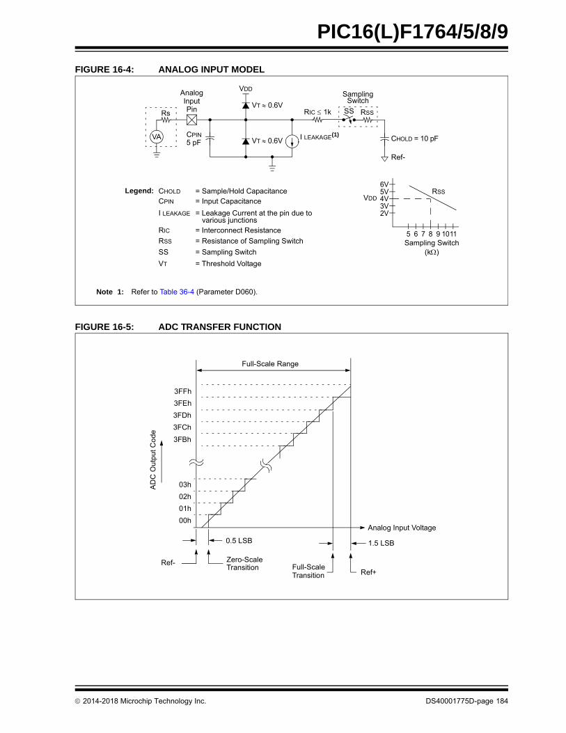
2014-2018 Microchip Technology Inc. DS40001775D-page 184
PIC16(L)F1764/5/8/9
FIGURE 16-4: ANALOG INPUT MODEL
FIGURE 16-5: ADC TRANSFER FUNCTION
CPIN
Rs
Analog
5 pF
VDD
VT 0.6V
VT 0.6V I LEAKAGE(1)
RIC 1k
SamplingSwitch
SS RSS
CHOLD = 10 pF
Ref-
6V
Sampling Switch
5V4V3V2V
5 6 7 8 9 1011
(k)
VDD
Legend:
CPIN
VT
I LEAKAGE
RIC
SS
CHOLD
= Input Capacitance
= Threshold Voltage
= Leakage Current at the pin due to
= Interconnect Resistance
= Sampling Switch
= Sample/Hold Capacitance
various junctions
RSS
Note 1: Refer to Table 36-4 (Parameter D060).
RSS = Resistance of Sampling Switch
InputPin
VA
3FFh
3FEh
AD
C O
utp
ut C
od
e
3FDh
3FCh
03h
02h
01h
00h
Full-Scale
3FBh
0.5 LSB
Ref- Zero-ScaleTransition
Ref+Transition
1.5 LSB
Full-Scale Range
Analog Input Voltage

2014-2018 Microchip Technology Inc. DS40001775D-page 185
PIC16(L)F1764/5/8/9
TABLE 16-3: SUMMARY OF REGISTERS ASSOCIATED WITH ADC
Name Bit 7 Bit 6 Bit 5 Bit 4 Bit 3 Bit 2 Bit 1 Bit 0Register on Page
ADCON0 — CHS<4:0> GO/DONE ADON 178
ADCON1 ADFM ADCS<2:0> — ADNREF ADPREF<1:0> 179
ADCON2 TRIGSEL<4:0> — — — 180
ADRESH ADC Result Register High 181, 182
ADRESL ADC Result Register Low 181, 182
ANSELA — — — ANSA4 — ANSA<2:0> 137
ANSELB(1) ANSB<7:6> ANSB<5:4> — — — — 143
ANSELC ANSC<7:6>(1) — — ANSC<3:0> 148
INTCON GIE PEIE TMR0IE INTE IOCIE TMR0IF INTF IOCIF 101
PIE1 TMR1GIE ADIE RCIE TXIE SSP1IE CCP1IE TMR2IE TMR1IE 102
PIR1 TMR1GIF ADIF RCIF TXIF SSP1IF CCP1IF TMR2IF TMR1IF 105
TRISA — — TRISA5 TRISA4 —(2) TRISA<2:0> 136
TRISB(1) TRISB<7:6> TRISB<5:4> — — — — 142
TRISC TRISC<7:6>(1) TRISC<5:4> TRISC<3:0> 147
FVRCON FVREN FVRRDY TSEN TSRNG CDAFVR<1:0> ADFVR<1:0> 169
DAC1CON0 EN FM OE1 — PSS<1:0> NSS<1:0> 188
Legend: — = unimplemented location, read as ‘0’. Shaded cells are not used for the ADC module.
Note 1: PIC16(L)F1768/9 only.
2: Unimplemented, read as ‘1’.

2014-2018 Microchip Technology Inc. DS40001775D-page 186
PIC16(L)F1764/5/8/9
17.0 5-BIT DIGITAL-TO-ANALOG CONVERTER (DAC) MODULE
The Digital-to-Analog Converter supplies a variablevoltage reference, ratiometric with the input source,with 32 selectable output levels.
The input of the DAC can be connected to:
• External VREF pins
• VDD supply voltage
• FVR (Fixed Voltage Reference)
The output of the DAC can be configured to supply areference voltage to the following:
• Comparator positive input
• Operational amplifier inverting and non-inverting inputs
• ADC input channel
• DACxOUT1 pin
The Digital-to-Analog Converter (DAC) is enabled bysetting the EN bit of the DACxCON0 register.
17.1 Output Voltage Selection
The DAC has 32 voltage level ranges. The 32 levelsare set with the REF<4:0> bits of the DACxREFregister.
The DAC output voltage is determined by Equation 17-1.
EQUATION 17-1: DAC OUTPUT VOLTAGE
17.2 Ratiometric Output Level
The DAC output value is derived using a resistor ladderwith each end of the ladder tied to a positive andnegative voltage reference input source. If the voltageof either input source fluctuates, a similar fluctuation willresult in the DAC output value.
The value of the individual resistors within the laddercan be found in Table 36-20.
17.3 DAC Voltage Reference Output
The DAC voltage can be output to the DACxOUT1 pinby setting the OE1 bit of the DACxCON0 register.Selecting the DAC voltage for output on theDACxOUT1 pin automatically overrides the digitaloutput buffer and digital input threshold detectorfunctions of that pin. Reading the DACxOUT1 pin whenit has been configured for DAC voltage output willalways return a ‘0’.
Due to the limited current drive capability, a buffer mustbe used on the DAC voltage output for externalconnections to the DACxOUT1 pin. Figure 17-2 showsan example buffering technique.
TABLE 17-1: AVAILABLE 5-BIT DACs
Device D3 D4
PIC16(L)F1764 ●
PIC16(L)F1765 ●
PIC16(L)F1768 ● ●
PIC16(L)F1769 ● ●
IF DACxEN = 1:
VSOURCE+ = VDD, VREF, or FVR Buffer2
VSOURCE- = VSS
VOUT VSOURCE+ VSOURCE-– DACxR 4:0
25
-------------------------------- VSOURCE-+=

2014-2018 Microchip Technology Inc. DS40001775D-page 187
PIC16(L)F1764/5/8/9
FIGURE 17-1: DIGITAL-TO-ANALOG CONVERTER BLOCK DIAGRAM
FIGURE 17-2: VOLTAGE REFERENCE OUTPUT BUFFER EXAMPLE
17.4 Operation During Sleep
The DAC continues to function during Sleep. When thedevice wakes up from Sleep through an interrupt or aWatchdog Timer time-out, the contents of theDACxCON0 register are not affected. To minimizecurrent consumption in Sleep mode, the voltagereference should be disabled.
17.5 Effects of a Reset
A device Reset affects the following:
• DAC is disabled.
• DAC output voltage is removed from the DACXOUT1 pin.
• The REF<4:0> voltage reference control bits are cleared.
32
-to
-1 M
UX
R<4:0>
R
VREF-
NSS
R
R
R
R
R
R
32
5
(To Comparator andADC Modules)
OE1
VDD
VREF+
PSS<1:0>2
EN
Steps
Digital-to-Analog Converter (DAC)
FVR_buffer2
R
VSOURCE-
VSOURCE+
VSS
DACX_Output
DACxOUT1
PIC® MCU
DACModule
R
VoltageReference
OutputImpedance
DACxOUT1+– Buffered DAC Output

2014-2018 Microchip Technology Inc. DS40001775D-page 188
PIC16(L)F1764/5/8/9
17.6 Register Definitions: DAC Control
Long bit name prefixes for the 5-bit DAC peripherals areshown in Table 17-2. Refer to Section 1.1 “Register andBit Naming Conventions” for more information.
TABLE 17-2: BIT NAME PREFIXES
Peripheral Bit Name Prefix
DAC3 DAC3
DAC4(1) DAC4
Note 1: PIC16(L)F1768/9 devices only.
REGISTER 17-1: DACxCON0: DACx CONTROL REGISTER 0
R/W-0/0 U-0 R/W-0/0 U-0 R/W-0/0 R/W-0/0 U-0 R/W-0/0
EN — OE1 — PSS<1:0> — NSS
bit 7 bit 0
Legend:
R = Readable bit W = Writable bit
u = Bit is unchanged x = Bit is unknown U = Unimplemented bit, read as ‘0’
‘1’ = Bit is set ‘0’ = Bit is cleared -n/n = Value at POR and BOR/Value at all other Resets
bit 7 EN: DACx Enable bit
1 = DACx is enabled0 = DACx is disabled
bit 6 Unimplemented: Read as ‘0’
bit 5 OE1: DACx Voltage Output Enable bit
1 = DACx voltage level is also an output on the DACxOUT1 pin0 = DACx voltage level is disconnected from the DACxOUT1 pin
bit 4 Unimplemented: Read as ‘0’
bit 3-2 PSS<1:0>: DACx Positive Source Select bits
11 = Reserved, do not use10 = FVR Buffer2 output01 = VREF+ pin00 = VDD
bit 1 Unimplemented: Read as ‘0’
bit 0 NSS: DACx Negative Source Select bit
1 = VREF- pin0 = VSS

2014-2018 Microchip Technology Inc. DS40001775D-page 189
PIC16(L)F1764/5/8/9
TABLE 17-3: SUMMARY OF REGISTERS ASSOCIATED WITH THE DACx MODULE
REGISTER 17-2: DACxREF: DACx REFERENCE VOLTAGE OUTPUT SELECT REGISTER
U-0 U-0 U-0 R/W-0/0 R/W-0/0 R/W-0/0 R/W-0/0 R/W-0/0
— — — REF<4:0>
bit 7 bit 0
Legend:
R = Readable bit W = Writable bit
u = Bit is unchanged x = Bit is unknown U = Unimplemented bit, read as ‘0’
‘1’ = Bit is set ‘0’ = Bit is cleared -n/n = Value at POR and BOR/Value at all other Resets
bit 7-5 Unimplemented: Read as ‘0’
bit 4-0 REF<4:0>: DACx Reference Voltage Output Select bits (see Equation 17-1)
Name Bit 7 Bit 6 Bit 5 Bit 4 Bit 3 Bit 2 Bit 1 Bit 0Register on Page
DAC3CON0 EN — OE1 — PSS<1:0> — NSS 188
DAC4CON0(1) EN --- OE1 --- PSS<1:0> --- NSS 188
DAC3REF --- --- --- REF<4:0> 189
DAC4REF(1) --- --- --- REF<4:0> 189
Legend: — = unimplemented location, read as ‘0’. Shaded cells are not used with the DACx module.
Note 1: PIC16(L)F1768/9 only.

2014-2018 Microchip Technology Inc. DS40001775D-page 190
PIC16(L)F1764/5/8/9
18.0 10-BIT DIGITAL-TO-ANALOG CONVERTER (DAC) MODULE
The 10-bit Digital-to-Analog Converter (DAC) suppliesa variable voltage reference, ratiometric with the inputsource, with 1024 selectable output levels.
The input of the DAC can be connected to:
• External VREF pins• VDD supply voltage• FVR (Fixed Voltage Reference)
The output of the DAC can be configured to supply areference voltage to the following:
• Comparator positive input• ADC input channel• DACxOUT1 pin• Op Amp
The Digital-to-Analog Converter is enabled by settingthe EN bit of the DACxCON0 register.
18.1 Output Voltage Level Selection
The DAC has 1024 voltage levels that are set by the10-bit reference selection word contained in theDACxREFH and DACxREFL registers. This 10-bitword can be left or right justified. See Section 18.4“DAC Reference Selection Justification” for moredetails.
The DAC output voltage can be determined withEquation 18-1.
EQUATION 18-1: DAC OUTPUT VOLTAGE
18.2 Ratiometric Output Voltage
The DAC output voltage is derived using a resistorladder with each end of the ladder tied to a positive andnegative voltage source. If the voltage of either inputsource fluctuates, a similar fluctuation will result in theDAC output value.
The value of the individual resistors within the laddercan be found in Table 36-20.
18.3 DAC Output
The DAC voltage is always available to the internalperipherals that use it. The DAC voltage can be outputto the DACxOUT1 pin by setting the OE1 bit of theDACxCON0 register. Selecting the DAC voltage foroutput on the DACxOUT1 pin automatically overridesthe digital output buffer and digital input thresholddetector functions of that pin. Reading the DACXOUT1pin when it has been configured for DAC voltage outputwill always return a ‘0’.
Due to the limited current drive capability, a buffer mustbe used on the DAC voltage output for externalconnections to either DACXOUT1 pin. Figure 18-3shows a buffering technique example.
18.4 DAC Reference Selection Justification
The DAC reference selection can be configured to be leftor right justified. When the FM bit of the DACxCON0register is set, the 10-bit word is left justified, such thatthe eight Most Significant bits fill the DACxREFH registerand the two Least Significant bits are left justified in theDACxREFL register. When the FM bit is cleared, the10-bit word is right justified, such that the eight LeastSignificant bits fill the DACxREFL register and the twoMost Significant bits are right justified in the DACxREFHregister. Refer to Figure 18-1.
The DACxREFL and DACxREFH registers aredouble-buffered. Writing to either register does not takeeffect immediately. Writing a ‘1’ to the DACxLD bit ofthe DACLD register transfers the contents of theDACxREFH and DACxREFL registers to the buffers,thereby changing all 10 bits of the DAC referenceselection simultaneously.
TABLE 18-1: AVAILABLE 10-BIT DACs
Device D1 D2
PIC16(L)F1764 ●
PIC16(L)F1765 ●
PIC16(L)F1768 ● ●
PIC16(L)F1769 ● ●
If EN = 1:
VSOURCE+ = VDD, VREF+, or FVR_buffer2
VSOURCE- = VSS OR VREF-
DACx_output VSOURCE+ VSOURCE-– DACxR 9:0
210
-------------------------------- VSOURCE-+=

2014-2018 Microchip Technology Inc. DS40001775D-page 191
PIC16(L)F1764/5/8/9
FIGURE 18-1: DAC JUSTIFICATION
FIGURE 18-2: DIGITAL-TO-ANALOG CONVERTER BLOCK DIAGRAM
Rev. 10-000 225A4/29/201 4R9 R8 R7 R6 R5 R4 R3 R2 R1 R0 0 0 0 0 0 0
DACxREFH DACxREFL
0 0 0 0 0 0 R9 R8 R7 R6 R5 R4 R3 R2 R1 R0
DACxREFH DACxREFL
FM = 1
FM = 0
R9 R8 R7 R6 R5 R4 R3 R2 R1 R0
DACxREF
0707
07 07
VREF+
VDD
FVR_buffer2
Reserved
PSS<1:0>
VSOURCE+
VSOURCE-
2
VSS
R
1024Steps
R
R
R
R
R
R
1024
-to-1
MU
X
To Peripherals
DACxOUT1
OE
DACx_output
EN
10
DACxREFH DACxREFL
write 1 toDACxLD bit
10-bit Latch(not visible to user)
Rev. 10-000 219A5/8/201 4
VREF-
NSS

2014-2018 Microchip Technology Inc. DS40001775D-page 192
PIC16(L)F1764/5/8/9
FIGURE 18-3: VOLTAGE REFERENCE OUTPUT BUFFER EXAMPLE
18.5 Operation During Sleep
When the device wakes up from Sleep as the result ofan interrupt or a Watchdog Timer time-out, the contentsof the DACxCON0 register are not affected. Tominimize current consumption in Sleep mode, thevoltage reference should be disabled.
18.6 Effects of a Reset
A device Reset affects the following:
• DAC is disabled
• DAC output voltage is removed from the DACxOUT1 pin
• The REF<9:0> reference selection bits are cleared
PIC® MCU
DACModule
R
VoltageReference
OutputImpedance
DACxOUT1+– Buffered DAC Output

2014-2018 Microchip Technology Inc. DS40001775D-page 193
PIC16(L)F1764/5/8/9
18.7 Register Definitions: DAC Control
Long bit name prefixes for the 10-bit DAC peripherals areshown in Table 18-2. Refer to Section 1.1 “Registerand Bit Naming Conventions” for more information.
TABLE 18-2: BIT NAME PREFIXES
Peripheral Bit Name Prefix
DAC1 DAC1
DAC2(1) DAC2
Note 1: PIC16(L)F1768/9 devices only.
REGISTER 18-1: DACxCON0: DACx CONTROL REGISTER 0
R/W-0/0 R/W-0/0 R/W-0/0 U-0 R/W-0/0 R/W-0/0 U-0 R/W-0/0
EN FM OE1 — PSS<1:0> — NSS
bit 7 bit 0
Legend:
R = Readable bit W = Writable bit
u = Bit is unchanged x = Bit is unknown U = Unimplemented bit, read as ‘0’
‘1’ = Bit is set ‘0’ = Bit is cleared -n/n = Value at POR and BOR/Value at all other Resets
bit 7 EN: DACx Enable bit
1 = DACx is enabled0 = DACx is disabled
bit 6 FM: DACx Reference Format bit
1 = DACx reference selection is left justified0 = DACx reference selection is right justified
bit 5 OE1: DACx Voltage Output Enable bit
1 = DACx voltage level is also an output on the DACxOUT1 pin0 = DACx voltage level is disconnected from the DACxOUT1 pin
bit 4 Unimplemented: Read as ‘0’
bit 3-2 PSS<1:0>: DACx Positive Source Select bits
11 = Reserved; do not use.10 = FVR_buffer201 = VREF+ pin00 = VDD
bit 1 Unimplemented: Read as ‘0’
bit 0 NSS: DACx Negative Source Select bit
1 = VREF- pin0 = VSS

2014-2018 Microchip Technology Inc. DS40001775D-page 194
PIC16(L)F1764/5/8/9
REGISTER 18-2: DACxREFH: DACx REFERENCE VOLTAGE SELECT HIGH REGISTER
R/W-0/0 R/W-0/0 R/W-0/0 R/W-0/0 R/W-0/0 R/W-0/0 R/W-0/0 R/W-0/0
REF<9:x> (x Depends on FM bit)
bit 7 bit 0
Legend:
R = Readable bit W = Writable bit
u = Bit is unchanged x = Bit is unknown U = Unimplemented bit, read as ‘0’
‘1’ = Bit is set ‘0’ = Bit is cleared -n/n = Value at POR and BOR/Value at all other Resets
When FM = 1 (left justified):
bit 7-0 REF<9:2>: DAC Reference Voltage Output Select bits
DACxOUT1 = f(REF<9:0>) (see Equation 18-1).
When FM = 0 (right justified):
bit 7-2 Unimplemented: Read as ‘0’
bit 1-0 REF<9:8>: DAC Reference Voltage Output Select bits
DACxOUT1 = f(REF<9:0>) (see Equation 18-1).
REGISTER 18-3: DACxREFL: DACx REFERENCE VOLTAGE SELECT LOW REGISTER
R/W-0/0 R/W-0/0 R/W-0/0 R/W-0/0 R/W-0/0 R/W-0/0 R/W-0/0 R/W-0/0
REF<x-1:0> (x Depends on FM bit)
bit 7 bit 0
Legend:
R = Readable bit W = Writable bit
u = Bit is unchanged x = Bit is unknown U = Unimplemented bit, read as ‘0’
‘1’ = Bit is set ‘0’ = Bit is cleared -n/n = Value at POR and BOR/Value at all other Resets
When FM = 1 (left justified):
bit 7-6 REF<1:0>: DAC Reference Voltage Output Select bits
DACxOUT1 = f(REF<9:0>) (see Equation 18-1).
bit 5-0 Unimplemented: Read as ‘0’
When FM = 0 (right justified):
bit 7-0 REF<7:0>: DAC Reference Voltage Output Select bits
DACxOUT1 = f(REF<9:0>) (see Equation 18-1).
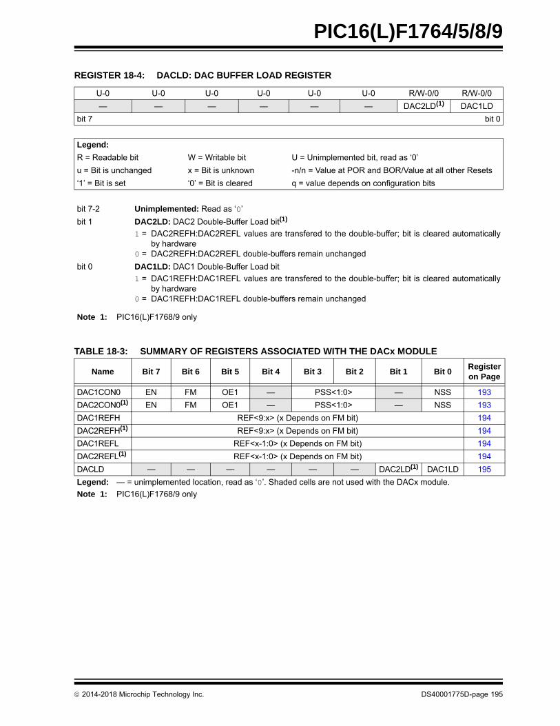
2014-2018 Microchip Technology Inc. DS40001775D-page 195
PIC16(L)F1764/5/8/9
TABLE 18-3: SUMMARY OF REGISTERS ASSOCIATED WITH THE DACx MODULE
REGISTER 18-4: DACLD: DAC BUFFER LOAD REGISTER
U-0 U-0 U-0 U-0 U-0 U-0 R/W-0/0 R/W-0/0
— — — — — — DAC2LD(1) DAC1LD
bit 7 bit 0
Legend:
R = Readable bit W = Writable bit U = Unimplemented bit, read as ‘0’
u = Bit is unchanged x = Bit is unknown -n/n = Value at POR and BOR/Value at all other Resets
‘1’ = Bit is set ‘0’ = Bit is cleared q = value depends on configuration bits
bit 7-2 Unimplemented: Read as ‘0’
bit 1 DAC2LD: DAC2 Double-Buffer Load bit(1)
1 = DAC2REFH:DAC2REFL values are transfered to the double-buffer; bit is cleared automaticallyby hardware
0 = DAC2REFH:DAC2REFL double-buffers remain unchanged
bit 0 DAC1LD: DAC1 Double-Buffer Load bit
1 = DAC1REFH:DAC1REFL values are transfered to the double-buffer; bit is cleared automaticallyby hardware
0 = DAC1REFH:DAC1REFL double-buffers remain unchanged
Note 1: PIC16(L)F1768/9 only
Name Bit 7 Bit 6 Bit 5 Bit 4 Bit 3 Bit 2 Bit 1 Bit 0Register on Page
DAC1CON0 EN FM OE1 — PSS<1:0> — NSS 193
DAC2CON0(1) EN FM OE1 — PSS<1:0> — NSS 193
DAC1REFH REF<9:x> (x Depends on FM bit) 194
DAC2REFH(1) REF<9:x> (x Depends on FM bit) 194
DAC1REFL REF<x-1:0> (x Depends on FM bit) 194
DAC2REFL(1) REF<x-1:0> (x Depends on FM bit) 194
DACLD — — — — — — DAC2LD(1) DAC1LD 195
Legend: — = unimplemented location, read as ‘0’. Shaded cells are not used with the DACx module.
Note 1: PIC16(L)F1768/9 only
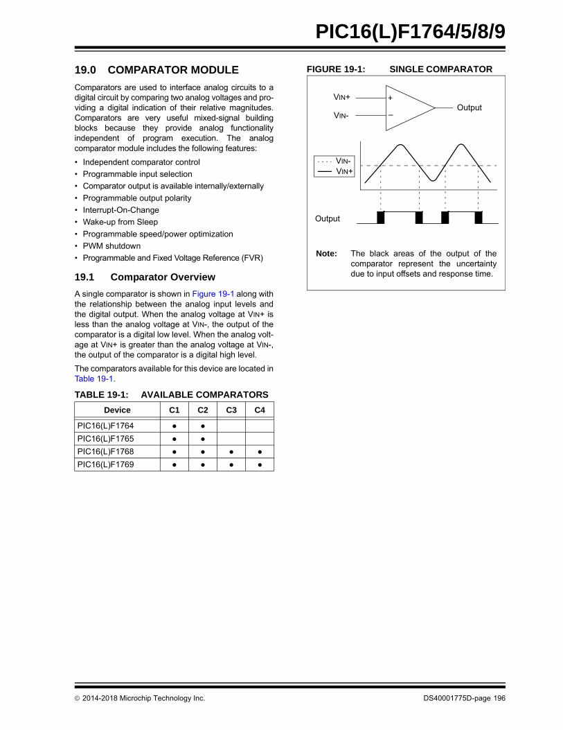
2014-2018 Microchip Technology Inc. DS40001775D-page 196
PIC16(L)F1764/5/8/9
19.0 COMPARATOR MODULE
Comparators are used to interface analog circuits to adigital circuit by comparing two analog voltages and pro-viding a digital indication of their relative magnitudes.Comparators are very useful mixed-signal buildingblocks because they provide analog functionalityindependent of program execution. The analogcomparator module includes the following features:
• Independent comparator control
• Programmable input selection
• Comparator output is available internally/externally
• Programmable output polarity
• Interrupt-On-Change
• Wake-up from Sleep
• Programmable speed/power optimization
• PWM shutdown
• Programmable and Fixed Voltage Reference (FVR)
19.1 Comparator Overview
A single comparator is shown in Figure 19-1 along withthe relationship between the analog input levels andthe digital output. When the analog voltage at VIN+ isless than the analog voltage at VIN-, the output of thecomparator is a digital low level. When the analog volt-age at VIN+ is greater than the analog voltage at VIN-,the output of the comparator is a digital high level.
The comparators available for this device are located inTable 19-1.
FIGURE 19-1: SINGLE COMPARATOR
TABLE 19-1: AVAILABLE COMPARATORS
Device C1 C2 C3 C4
PIC16(L)F1764 ● ●
PIC16(L)F1765 ● ●
PIC16(L)F1768 ● ● ● ●
PIC16(L)F1769 ● ● ● ●
–
+VIN+
VIN-Output
Output
VIN+VIN-
Note: The black areas of the output of thecomparator represent the uncertaintydue to input offsets and response time.

2014-2018 Microchip Technology Inc. DS40001775D-page 197
PIC16(L)F1764/5/8/9
FIGURE 19-2: COMPARATOR MODULE SIMPLIFIED BLOCK DIAGRAM
Note 1: When CxON = 0, the comparator will produce a ‘0’ at the output.
2: When CxON = 0, all multiplexer inputs are disconnected.
3: Only on PIC16(L)F1768/9
MUX(2)
Cx
CxON(1)CxNCH<2:0>3
0
1
CxPCH<3:0>
CxIN1-
CxIN2-
CxIN3-
CxIN0+
MUX(2)
–
+
CxVN
CxVP Q1
Set CxIF
CxSYNC
CxOUT
DAC4_output(3)
FVR Buffer2
CxIN0-
10
CxHYS
CxINTN
CxINTP
4
11
AGND
TRISx bit
CxON
From Timer1tmr1_clk
FVR Buffer2
0
1
2
3
4
5
6
7AGND
12
13
14
15
PRG2_output(3)
sync_CxOUT
To CMxCON0 (CXOUT)and CM2CON1 (MCxOUT)
CxPOL
0
1
CxZLF
PRG1_output
CxIN1+(3)
DAC3_output
DAC2_output(3)
DAC1_output
9PRG2_output(3)
8PRG1_output
7
2
Reserved
To ADC, PRG, CLC,Timer1/3/5 Gate,Timer2/4/6 Reset,
0
1PPS
RxyPPS
COG, DSM
ZLF
Interrupt
det
Interrupt
det
D
EN
Q
D Q

2014-2018 Microchip Technology Inc. DS40001775D-page 198
PIC16(L)F1764/5/8/9
19.2 Comparator Control
Each comparator has two control registers: CMxCON0and CMxCON1.
The CMxCON0 register (see Register 19-1) containscontrol and status bits for the following:
• Enable
• Output
• Output polarity
• Zero latency filter
• Speed/power selection
• Hysteresis enable
• Output synchronization
The CMxCON1 register (see Register 19-2) containscontrol bits for the following:
• Interrupt enable
• Interrupt edge polarity
• Positive input channel selection
• Negative input channel selection
19.2.1 COMPARATOR ENABLE
Setting the ON bit of the CMxCON0 register enables thecomparator for operation. Clearing the ON bit disables thecomparator, resulting in minimum current consumption.
19.2.2 COMPARATOR OUTPUT SELECTION
The output of the comparator can be monitored byreading either the OUT bit of the CMxCON0 register orthe MCxOUT bit of the CMOUT register. In order tomake the output available for an external connection,the following conditions must be true:
• Desired pin PPS control
• Corresponding TRISx bit must be cleared
• ON bit of the CMxCON0 register must be set
19.2.3 COMPARATOR OUTPUT POLARITY
Inverting the output of the comparator is functionallyequivalent to swapping the comparator inputs. Thepolarity of the comparator output can be inverted bysetting the POL bit of the CMxCON0 register. Clearingthe POL bit results in a non-inverted output.
Table 19-2 shows the output state versus inputconditions, including polarity control.
Note 1: The internal output of the comparator islatched with each instruction cycle.Unless otherwise specified, externaloutputs are not latched.
TABLE 19-2: COMPARATOR OUTPUT STATE vs. INPUT CONDITIONS
Input Condition CxPOL CxOUT
CxVN > CxVP 0 0
CxVN < CxVP 0 1
CxVN > CxVP 1 1
CxVN < CxVP 1 0

2014-2018 Microchip Technology Inc. DS40001775D-page 199
PIC16(L)F1764/5/8/9
19.3 Comparator Hysteresis
A selectable amount of separation voltage can beadded to the input pins of each comparator to provide ahysteresis function to the overall operation. Hysteresisis enabled by setting the HYS bit of the CMxCON0register.
See Comparator Specifications in Table 36-19:Comparator Specifications for more information.
19.4 Timer1 Gate Operation
The output resulting from a comparator operation canbe used as a source for gate control of Timer1. SeeSection 22.6 “Timer1 Gate” for more information.This feature is useful for timing the duration or intervalof an analog event.
It is recommended that the comparator output besynchronized to Timer1. This ensures that Timer1 doesnot increment while a change in the comparator isoccurring.
19.4.1 COMPARATOR OUTPUT SYNCHRONIZATION
The output from a comparator can be synchronizedwith Timer1 by setting the SYNC bit of the CMxCON0register.
Once enabled, the comparator output is latched on thefalling edge of the Timer1 source clock. If a prescaler isused with Timer1, the comparator output is latched afterthe prescaling function. To prevent a race condition, thecomparator output is latched on the falling edge of theTimer1 clock source and Timer1 increments on therising edge of its clock source. See the ComparatorBlock Diagram (Figure 19-2) and the Timer1 BlockDiagram (Figure 22-1) for more information.
19.5 Comparator Interrupt
An interrupt can be generated upon a change in theoutput value of the comparator for each comparator, arising edge detector and a falling edge detector arepresent.
When either edge detector is triggered and its associ-ated enable bit is set (INTP and/or INTN bits of theCMxCON1 register), the corresponding interrupt flagbit (CxIF bit of the PIR2 register) will be set.
To enable the interrupt, you must set the following bits:
• ON and POL bits of the CMxCON0 register
• CxIE bit of the PIE2 register
• INTP bit of the CMxCON1 register (for a rising edge detection)
• INTN bit of the CMxCON1 register (for a falling edge detection)
• PEIE and GIE bits of the INTCON register
The associated interrupt flag bit, CxIF bit of the PIR2register, must be cleared in software. If another edge isdetected while this flag is being cleared, the flag will stillbe set at the end of the sequence.
19.6 Comparator Positive Input Selection
Configuring the PCH<3:0> bits of the CMxPSELregister directs an internal voltage reference or ananalog pin to the non-inverting input of the comparator:
• CxIN+ analog pin
• Programmable Ramp Generator (PRG) output
• DAC output
• FVR (Fixed Voltage Reference)
• VSS (Ground)
See Section 14.0 “Fixed Voltage Reference (FVR)”for more information on the Fixed Voltage Referencemodule.
See Section 17.0 “5-Bit Digital-to-Analog Converter(DAC) Module” for more information on the DAC inputsignal.
Any time the comparator is disabled (CxON = 0), allcomparator inputs are disabled.
19.7 Comparator Negative Input Selection
The NCH<2:0> bits of the CMxNSEL register direct ananalog input pin and internal reference voltage oranalog ground to the inverting input of the comparator:
• CxIN- pin
• FVR (Fixed Voltage Reference)
• Analog ground
Some inverting input selections share a pin with theoperational amplifier output function. Enabling bothfunctions at the same time will direct the operationalamplifier output to the comparator inverting input.
Note: Although a comparator is disabled, aninterrupt can be generated by changingthe output polarity with the POL bit of theCMxCON0 register, or by switching thecomparator on or off with the ON bit of theCMxCON0 register.
Note: To use CxINy+ and CxINy- pins as analoginputs, the appropriate bits must be set inthe ANSELx register and the correspond-ing TRISx bits must also be set to disablethe output drivers.

2014-2018 Microchip Technology Inc. DS40001775D-page 200
PIC16(L)F1764/5/8/9
19.8 Comparator Response Time
The comparator output is indeterminate for a period oftime after the change of an input source or the selectionof a new reference voltage. This period is referred to asthe response time. The response time of the comparatordiffers from the settling time of the voltage reference.Therefore, both of these times must be considered whendetermining the total response time to a comparatorinput change. See the Comparator and VoltageReference Specifications in Table 36-19: ComparatorSpecifications for more details.
19.9 Zero Latency Filter
In high-speed operation, and under proper circuitconditions, it is possible for the comparator output tooscillate. This oscillation can have adverse effects on
the hardware and software relying on this signal.Therefore, a digital filter has been added to thecomparator output to suppress the comparator outputoscillation. Once the comparator output changes, theoutput is prevented from reversing the change for anominal time of 20 ns. This allows the comparatoroutput to stabilize without affecting other dependentdevices. Refer to Figure 19-3.
FIGURE 19-3: COMPARATOR ZERO LATENCY FILTER OPERATION
CxOUT from Comparator
CxOUT from ZLFTZLF
Output waiting for TZLF to expire before an output change is allowed.
TZLF has expired so output change of ZLF is immediate based oncomparator output change.

2014-2018 Microchip Technology Inc. DS40001775D-page 201
PIC16(L)F1764/5/8/9
19.10 Analog Input Connection Considerations
A simplified circuit for an analog input is shown inFigure 19-4. Since the analog input pins share theirconnection with a digital input, they have reversebiased ESD protection diodes to VDD and VSS. Theanalog input, therefore, must be between VSS and VDD.If the input voltage deviates from this range by morethan 0.6V in either direction, one of the diodes isforward biased and a latch-up may occur.
A maximum source impedance of 10 k is recommendedfor the analog sources. Also, any external componentconnected to an analog input pin, such as a capacitor ora Zener diode, should have very little leakage current tominimize inaccuracies introduced.
FIGURE 19-4: ANALOG INPUT MODEL
Note 1: When reading a PORT register, all pinsconfigured as analog inputs will read as a‘0’. Pins configured as digital inputs willconvert as an analog input, according tothe input specification.
2: Analog levels on any pin defined as adigital input, may cause the input buffer toconsume more current than is specified.
Note 1: See I/O Ports in Table 36-4: I/O Ports.
VA
RS < 10K
VDD
Analog Input pin
CPIN 5pF
VT 0.6V
VT 0.6V
ILEAKAGE(1)
VSS
RICTo Comparator
Legend: CPIN = Input CapacitanceILEAKAGE = Leakage Current at the pin due to various junctionsRIC = Interconnect ResistanceRS = Source ImpedanceVA = Analog VoltageVT = Threshold Voltage
Rev. 10-000071A8/2/2013

2014-2018 Microchip Technology Inc. DS40001775D-page 202
PIC16(L)F1764/5/8/9
19.11 Register Definitions: Comparator Control
Long bit name prefixes for the DSM peripherals areshown in Table 19-3. Refer to Section 1.1.2.2 “LongBit Names” for more information
TABLE 19-3: BIT NAME PREFIXES
Peripheral Bit Name Prefix
Comparator 1 C1
Comparator 2(1) C2
Note 1: PIC16(L)F1768/9 devices only.
REGISTER 19-1: CMxCON0: COMPARATOR Cx CONTROL REGISTER 0
R/W-0/0 R-0/0 U-0 R/W-0/0 R/W-0/0 R/W-1/1 R/W-0/0 R/W-0/0
ON OUT — POL ZLF r HYS SYNC
bit 7 bit 0
Legend:
R = Readable bit W = Writable bit r = Reserved bit
u = Bit is unchanged x = Bit is unknown U = Unimplemented bit, read as ‘0’
‘1’ = Bit is set ‘0’ = Bit is cleared -n/n = Value at POR and BOR/Value at all other Resets
bit 7 ON: Comparator Enable bit
1 = Comparator is enabled0 = Comparator is disabled and consumes no active power
bit 6 OUT: Comparator Output bit
If POL = 1 (inverted polarity):1 = CxVP < CxVN0 = CxVP > CxVN
If POL = 0 (non-inverted polarity):1 = CxVP > CxVN0 = CxVP < CxVN
bit 5 Unimplemented: Read as ‘0’
bit 4 POL: Comparator Output Polarity Select bit
1 = Comparator output is inverted0 = Comparator output is not inverted
bit 3 ZLF: Comparator Zero Latency Filter Enable bit
1 = Comparator output is filtered0 = Comparator output is unfiltered
bit 2 Reserved: Read as ‘1’; maintain this bit set
bit 1 HYS: Comparator Hysteresis Enable bit
1 = Comparator hysteresis is enabled0 = Comparator hysteresis is disabled
bit 0 SYNC: Comparator Output Synchronous Mode bit
1 = Comparator output to Timer1 and I/O pin is synchronous to changes on Timer1 clock source;output updated on the falling edge of Timer1 clock source
0 = Comparator output to Timer1 and I/O pin is asynchronous

2014-2018 Microchip Technology Inc. DS40001775D-page 203
PIC16(L)F1764/5/8/9
REGISTER 19-2: CMxCON1: COMPARATOR Cx CONTROL REGISTER 1
U-0 U-0 U-0 U-0 U-0 U-0 R/W-0/0 R/W-0/0
— — — — — — INTP INTN
bit 7 bit 0
Legend:
R = Readable bit W = Writable bit
u = Bit is unchanged x = Bit is unknown U = Unimplemented bit, read as ‘0’
‘1’ = Bit is set ‘0’ = Bit is cleared -n/n = Value at POR and BOR/Value at all other Resets
bit 7-2 Unimplemented: Read as ‘0’
bit 1 INTP: Comparator Interrupt on Positive Going Edge Enable bit
1 = The CxIF interrupt flag will be set upon a positive going edge of the CxOUT bit0 = No interrupt flag will be set on a positive going edge of the CxOUT bit
bit 0 INTN: Comparator Interrupt on Negative Going Edge Enable bit
1 = The CxIF interrupt flag will be set upon a negative going edge of the CxOUT bit0 = No interrupt flag will be set on a negative going edge of the CxOUT bit
REGISTER 19-3: CMxNSEL: COMPARATOR Cx NEGATIVE CHANNEL SELECT REGISTER
U-0 U-0 U-0 U-0 U-0 R/W-0/0 R/W-0/0 R/W-0/0
— — — — — NCH<2:0>
bit 7 bit 0
Legend:
R = Readable bit W = Writable bit
u = Bit is unchanged x = Bit is unknown U = Unimplemented bit, read as ‘0’
‘1’ = Bit is set ‘0’ = Bit is cleared -n/n = Value at POR and BOR/Value at all other Resets
bit 7-3 Unimplemented: Read as ‘0’
bit 2-0 NCH<2:0>: Comparator Negative Input Channel Select bits
111 = CxVN connects to AGND110 = CxVN connects to FVR Buffer2101 = CxVN connects to PRG2_output(1)
100 = CxVN connects to PRG1_output011 = CxVN connects to CxIN3- pin010 = CxVN connects to CxIN2- pin001 = CxVN connects to CxIN1- pin000 = CxVN connects to CxIN0- pin
Note 1: PIC16(L)F1768/9 only.

2014-2018 Microchip Technology Inc. DS40001775D-page 204
PIC16(L)F1764/5/8/9
REGISTER 19-4: CMxPSEL: COMPARATOR Cx POSITIVE CHANNEL SELECT REGISTER 1
U-0 U-0 U-0 U-0 R/W-0/0 R/W-0/0 R/W-0/0 R/W-0/0
— — — — PCH<3:0>
bit 7 bit 0
Legend:
R = Readable bit W = Writable bit
u = Bit is unchanged x = Bit is unknown U = Unimplemented bit, read as ‘0’
‘1’ = Bit is set ‘0’ = Bit is cleared -n/n = Value at POR and BOR/Value at all other Resets
bit 7-4 Unimplemented: Read as ‘0’
bit 3-0 PCH<3:0>: Comparator Positive Input Channel Select bits
1111 = CxVP connects to AGND1110 = CxVP connects to FVR Buffer21101 = CxVP connects to DAC4_output(1)
1100 = CxVP connects to DAC3_output1011 = CxVP connects to DAC2_output(1)
1010 = CxVP connects to DAC1_output1001 = CxVP connects to PRG2_output(1)
1000 = CxVP connects to PRG1_output0111 = CxVP unconnected, input floating0110 = CxVP unconnected, input floating0101 = CxVP unconnected, input floating0100 = CxVP unconnected, input floating0011 = CxVP unconnected, input floating0010 = CxVP unconnected, input floating0001 = CxVP connects to CxIN1+ pin0000 = CxVP connects to CxIN0+ pin
Note 1: PIC16(L)F1768/9 only.
Note: There are no long and short bit name variants for the following mirror register.
REGISTER 19-5: CMOUT: COMPARATOR OUTPUT REGISTER
U-0 U-0 U-0 U-0 R-0/0 R-0/0 R-0/0 R-0/0
— — — — MC4OUT(1) MC3OUT(1) MC2OUT MC1OUT
bit 7 bit 0
Legend:
R = Readable bit W = Writable bit
u = Bit is unchanged x = Bit is unknown U = Unimplemented bit, read as ‘0’
‘1’ = Bit is set ‘0’ = Bit is cleared -n/n = Value at POR and BOR/Value at all other Resets
bit 7-2 Unimplemented: Read as ‘0’
bit 3 MC4OUT: Mirror Copy of C4OUT bit(1)
bit 2 MC3OUT: Mirror Copy of C3OUT bit(1)
bit 1 MC2OUT: Mirror Copy of C2OUT bit
bit 0 MC1OUT: Mirror Copy of C1OUT bit
Note 1: PIC16(L)F1768/9 only.
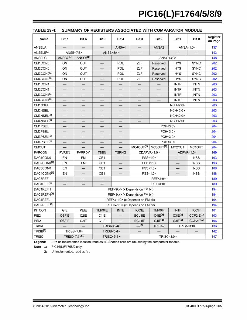
2014-2018 Microchip Technology Inc. DS40001775D-page 205
PIC16(L)F1764/5/8/9
TABLE 19-4: SUMMARY OF REGISTERS ASSOCIATED WITH COMPARATOR MODULE
Name Bit 7 Bit 6 Bit 5 Bit 4 Bit 3 Bit 2 Bit 1 Bit 0Register on Page
ANSELA — — — ANSA4 — ANSA2 ANSA<1:0> 137
ANSELB(1) ANSB<7:6> ANSB<5:4> — — — — 143
ANSELC ANSC7(1) ANSC6(1) — — ANSC<3:0> 148
CM1CON0 ON OUT — POL ZLF Reserved HYS SYNC 202
CM2CON0 ON OUT — POL ZLF Reserved HYS SYNC 202
CM3CON0(1) ON OUT — POL ZLF Reserved HYS SYNC 202
CM4CON0(1) ON OUT — POL ZLF Reserved HYS SYNC 202
CM1CON1 — — — — — — INTP INTN 203
CM2CON1 — — — — — — INTP INTN 203
CM3CON1(1) — — — — — — INTP INTN 203
CM4CON1(1) — — — — — — INTP INTN 203
CM1NSEL — — — — — NCH<2:0> 203
CM2NSEL — — — — — NCH<2:0> 203
CM3NSEL(1) — — — — — NCH<2:0> 203
CM4NSEL(1) — — — — — NCH<2:0> 203
CM1PSEL — — — — PCH<3:0> 204
CM2PSEL — — — — PCH<3:0> 204
CM3PSEL(1) — — — — PCH<3:0> 204
CM4PSEL(1) — — — — PCH<3:0> 204
CMOUT — — — — MC4OUT(1) MC3OUT(1) MC2OUT MC1OUT 204
FVRCON FVREN FVRRDY TSEN TSRNG CDAFVR<1:0> ADFVR<1:0> 169
DAC1CON0 EN FM OE1 — PSS<1:0> — NSS 193
DAC2CON0(1) EN FM OE1 — PSS<1:0> — NSS 193
DAC3CON0 EN — OE1 — PSS<1:0> — NSS 188
DAC4CON0(1) EN — OE1 — PSS<1:0> — NSS 188
DAC3REF --- --- --- REF<4:0> 189
DAC4REF(1) --- --- --- REF<4:0> 189
DAC1REFH REF<9:x> (x Depends on FM bit) 194
DAC2REFH(1) REF<9:x> (x Depends on FM bit) 194
DAC1REFL REF<x-1:0> (x Depends on FM bit) 194
DAC2REFL(1) REF<x-1:0> (x Depends on FM bit) 194
INTCON GIE PEIE TMR0IE INTE IOCIE TMR0IF INTF IOCIF 101
PIE2 OSFIE C2IE C1IE — BCL1IE C4IE(1) C3IE(1) CCP2IE(1) 103
PIR2 OSFIF C2IF C1IF — BCL1IF C4IF(1) C3IF(1) CCP2IF(1) 106
TRISA — — TRISA<5:4> —(2) TRISA2 TRISA<1:0> 136
TRISB(1) TRISB<7:6> TRISB<5:4> — — — — 142
TRISC TRISC<7:6>(1) TRISC<5:4> TRISC<3:0> 147
Legend: — = unimplemented location, read as ‘0’. Shaded cells are unused by the comparator module.
Note 1: PIC16(L)F1768/9 only.
2: Unimplemented, read as ‘1’.

2014-2018 Microchip Technology Inc. DS40001775D-page 206
PIC16(L)F1764/5/8/9
20.0 ZERO-CROSS DETECTION (ZCD) MODULE
The ZCD module detects when an A/C signal crossesthrough the ground potential. The actual zero-crossingthreshold is the zero-crossing reference voltage,ZCPINV, which is typically 0.75V above ground.
The connection to the signal to be detected is througha series current-limiting resistor. The module applies acurrent source or sink to the ZCD pin to maintain aconstant voltage on the pin, thereby preventing the pinvoltage from forward biasing the ESD protectiondiodes. When the applied voltage is greater than thereference voltage, the module sinks current. When theapplied voltage is less than the reference voltage, themodule sources current. The current source and sinkaction keeps the pin voltage constant over the fullrange of the applied voltage. The ZCD module isshown in the simplified block diagram (Figure 20-2).
The ZCD module is useful when monitoring an ACwaveform for, but not limited to, the following purposes:
• A/C period measurement
• Accurate long term time measurement
• Dimmer phase delayed drive
• Low EMI cycle switching
20.1 External Resistor Selection
The ZCD module requires a current-limiting resistor inseries with the external voltage source. The impedanceand rating of this resistor depends on the externalsource peak voltage. Select a resistor value that willdrop all of the peak voltage when the current throughthe resistor is nominally 300 A. Refer to Equation 20-1and Figure 20-1. Make sure that the ZCD I/O pininternal weak pull-up is disabled so it doesn’t interferewith the current source and sink.
EQUATION 20-1: EXTERNAL RESISTOR
FIGURE 20-1: EXTERNAL VOLTAGE
FIGURE 20-2: SIMPLIFIED ZCD BLOCK DIAGRAM
Rseries
Vpeak
34–
10------------------=
Vpeak
ZCPINV
maxpeakminpeak
ZCD Pin+
–
ZCPINV
ExternalCurrent-Limiting
ExternalVoltageSource
Interrupt
det
Interrupt
det
INTP
INTN
SetsZCDIF Flag
OUT
Q1
D Q
LE
POL
ZCDx_output
VDD
Rseries
Rpullup
VpullupOptional
Rpulldown
Optional
Resistor

2014-2018 Microchip Technology Inc. DS40001775D-page 207
PIC16(L)F1764/5/8/9
20.2 ZCD Logic Output
The ZCD module includes a status bit, which can beread to determine whether the current source or sink isactive. The OUT bit of the ZCDCON register is setwhen the current sink is active, and cleared when thecurrent source is active. The OUT bit is affected by thepolarity bit.
20.3 ZCD Logic Polarity
The POL bit of the ZCDxCON register inverts the OUTbit relative to the current source and sink output. Whenthe POL bit is set, a OUT high indicates that the currentsource is active, and a low output indicates that thecurrent sink is active.
The POL bit affects the ZCD interrupts. SeeSection 20.4 “ZCD Interrupts”.
20.4 ZCD Interrupts
An interrupt will be generated upon a change in theZCD logic output when the appropriate interruptenables are set. A rising edge detector and a fallingedge detector are present in the ZCD for this purpose.
The ZCDIF bit of the PIR3 register will be set wheneither edge detector is triggered and its associatedenable bit is set. The INTP enables rising edge inter-rupts and the INTN bit enables falling edge interrupts.Both are located in the ZCDxCON register.
To fully enable the interrupt, the following bits mustbe set:
• ZCDIE bit of the PIE3 register
• INTP bit of the ZCDxCON register (for a rising edge detection)
• INTN bit of the ZCDxCON register (for a falling edge detection)
• PEIE and GIE bits of the INTCON register
Changing the POL bit will cause an interrupt,regardless of the level of the EN bit.
The ZCDIF bit of the PIR3 register must be cleared insoftware as part of the interrupt service. If another edgeis detected while this flag is being cleared, the flag willstill be set at the end of the sequence.
20.5 Correcting for ZCPINV Offset
The actual voltage at which the ZCD switches is thereference voltage at the non-inverting input of the ZCDop amp. For external voltage source waveforms otherthan square waves this voltage offset from zero causesthe zero-cross event to occur either too early or toolate.
20.5.1 CORRECTION BY AC COUPLING
When the external voltage source is sinusoidal, theeffects of the ZCPINV offset can be eliminated byisolating the external voltage source from the ZCD pinwith a capacitor in addition to the voltage reducingresistor. The capacitor will cause a phase shift resultingin the ZCD output switch in advance of the actualzero-crossing event. The phase shift will be the samefor both rising and falling zero crossings, which can becompensated for by either delaying the CPU responseto the ZCD switch by a timer or other means, orselecting a capacitor value large enough that the phaseshift is negligible.
To determine the series resistor and capacitor valuesfor this configuration, start by computing theimpedance, Z, to obtain a peak current of 300 A. Next,arbitrarily select a suitably large non-polar capacitorand compute its reactance, XC, at the external voltagesource frequency. Finally, compute the series resistor,capacitor peak voltage, and phase shift by the formulasshown in Equation 20-2.

2014-2018 Microchip Technology Inc. DS40001775D-page 208
PIC16(L)F1764/5/8/9
EQUATION 20-2: R-C CALCULATIONS EQUATION 20-3: R-C CALCULATIONS EXAMPLE
Vpeak = external voltage source peak voltage
f = external voltage source frequency
C = series capacitor
R = series resistor
VC = Peak capacitor voltage
= Capacitor induced zero crossing phaseadvance in radians
T = Time ZC event occurs before actual zerocrossing
ZVPEAK
3x10⁴–
-----------------=
XC
12fC
-----------------=
R Z2
XC2
–=
VC XC 3x10⁴– =
Tan1– XC
R------ =
T
2f -------------=
Vrms = 120
f = 60 Hz
C = 0.1 f
R = 560 kOhms (used)
Vpeak Vrms 2 169.7==
ZVpeak
3 104–
---------------------
169.7
3 104–
--------------------- 565.7 kOhms===
XC
12fC
-----------------1
2 60 1 107–
---------------------------------------------- 26.53 kOhms===
ZR
R2
Xc2+
560.6 kOhm using actual resistor ==
Ipeak
VpeakZ
R
---------------- 302.7 106–
= =
VC
XC
Ipeak 8.0 V= =
Tan1– X
C
R------- 0.047 radians= =
T
2f ------------- 125.6 s==
R Z2
XC2
– 565.1k Ohms (computed)= =

2014-2018 Microchip Technology Inc. DS40001775D-page 209
PIC16(L)F1764/5/8/9
20.5.2 CORRECTION BY OFFSET CURRENT
When the waveform is varying relative to Vss then thezero cross is detected too early as the waveform fallsand too late as the waveform rises. When thewaveform is varying relative to VDD then the zero crossis detected too late as the waveform rises and too earlyas the waveform falls. The actual offset time can bedetermined for sinusoidal waveforms with thecorresponding equations shown in Equation 20-4.
EQUATION 20-4: ZCD EVENT OFFSET
This offset time can be compensated for by adding apull-up or pull-down biasing resistor to the ZCD pin. Apull-up resistor is used when the external voltagesource is varying relative to Vss. A pull-down resistor isused when the voltage is varying relative to VDD.Theresistor adds a bias to the ZCD pin so that the targetexternal voltage source must go to zero to pull the pinvoltage to the ZCPINV switching voltage. The pull-up orpull-down value can be determined with the equationsshown in Equation 20-5.
EQUATION 20-5: ZCD PULL-UP/DOWN
20.6 Handling VPEAK variations
If the peak amplitude of the external voltage isexpected to vary then the series resistor must beselected to keep the ZCD current source and sinkbelow the design maximum range of ± 600 A for themaximum expected voltage and high enough to bedetected accurately at the minimum peak voltage. Ageneral rule of thumb is that the maximum peak voltagecan be no more than six times the minimum peakvoltage. To ensure that the maximum current does notexceed ± 600 A and the minimum is at least ± 100 A,compute the series resistance as shown inEquation 20-6. The compensating pull-up for this seriesresistance can be determined with Equation 20-5because the pull-up value is independent from the peakvoltage.
EQUATION 20-6: SERIES R FOR V RANGE
20.7 Operation During Sleep
The ZCD current sources and interrupts are unaffectedby Sleep.
20.8 Effects of a Reset
The ZCD circuit can be configured to default to the activeor inactive state on Power-on Reset (POR). When theZCD Configuration bit is cleared, the ZCD circuit will beactive at POR. When the ZCD Configuration bit is set,the EN bit of the ZCDxCON register must be set toenable the ZCD module.
Toffset
ZcpinvVpeak-----------------
asin
2 Freq----------------------------------=
When External Voltage Source is relative to Vss:
Toffset
VDD Zcpinv–
Vpeak--------------------------------
asin
2 Freq-------------------------------------------------=
When External Voltage Source is relative to VDD:
Rpullup
Rseries Vpullup Zcpinv–
Zcpinv---------------------------------------------------------------------=
When External Signal is relative to Vss:
When External Signal is relative to VDD:
Rpulldown
Rseries Zcpinv
VDD Zcpinv– ------------------------------------------=
Rseries
Vmaxpeak Vminpeak+
74–
10------------------------------------------------------------=

2014-2018 Microchip Technology Inc. DS40001775D-page 210
PIC16(L)F1764/5/8/9
20.9 Register Definitions: ZCD ControlLong bit name prefixes for the Zero-Cross Detect periph-eral are shown in Table 20-1. Refer to Section 1.1.2.2“Long Bit Names” for more information
TABLE 20-1: BIT NAME PREFIXES
Peripheral Bit Name Prefix
ZCD1 ZCD1
REGISTER 20-1: ZCDxCON: ZERO-CROSS DETECTION x CONTROL REGISTER
R/W-0/0 U-0 R-x/x R/W-0/0 U-0 U-0 R/W-0/0 R/W-0/0
EN(1) — OUT POL — — INTP INTN
bit 7 bit 0
Legend:
R = Readable bit W = Writable bit U = Unimplemented bit, read as ‘0’
u = Bit is unchanged x = Bit is unknown -n/n = Value at POR and BOR/Value at all other Resets
‘1’ = Bit is set ‘0’ = Bit is cleared q = value depends on configuration bits
bit 7 EN: Zero-Cross Detection Enable bit(1)
1 = Zero-Cross Detect is enabled; ZCD pin is forced to output to source and sink current0 = Zero-Cross Detect is disabled; ZCD pin operates according to PPS and TRISx controls
bit 6 Unimplemented: Read as ‘0’
bit 5 OUT: Zero-Cross Detection Logic Level bit
POL bit = 0:1 = ZCD pin is sinking current0 = ZCD pin is sourcing current
POL bit = 1:1 = ZCD pin is sourcing current0 = ZCD pin is sinking current
bit 4 POL: Zero-Cross Detection Logic Output Polarity bit
1 = ZCD logic output is inverted0 = ZCD logic output is not inverted
bit 3-2 Unimplemented: Read as ‘0’
bit 1 INTP: Zero-Cross Positive Edge Interrupt Enable bit
1 = ZCDIF bit is set on low-to-high OUT transition0 = ZCDIF bit is unaffected by low-to-high OUT transition
bit 0 INTN: Zero-Cross Negative Edge Interrupt Enable bit
1 = ZCDIF bit is set on high-to-low OUT transition0 = ZCDIF bit is unaffected by high-to-low OUT transition
Note 1: The EN bit has no effect when the ZCD Configuration bit is cleared.

2014-2018 Microchip Technology Inc. DS40001775D-page 211
PIC16(L)F1764/5/8/9
TABLE 20-2: SUMMARY OF REGISTERS ASSOCIATED WITH THE ZCD MODULE
Name Bit 7 Bit 6 Bit 5 Bit 4 Bit 3 Bit 2 Bit 1 Bit 0Register on page
PIE3 PWM6IE(1) PWM5IE COG1IE ZCDIE COG2IE(1) CLC3IE CLC2IE CLC1IE 104
PIR3 PWM6IF(1) PWM5IF COG1IF ZCDIF COG2IF(1) CLC3IF CLC2IF CLC1IF 107
ZCD1CON EN — OUT POL — — INTP INTN 210
Legend: — = unimplemented, read as ‘0’. Shaded cells are unused by the ZCD module.
Note 1: PIC16(L)F1768/9 only.
TABLE 20-3: SUMMARY OF CONFIGURATION WORD WITH THE ZCD MODULE
Name Bits Bit -/7 Bit -/6 Bit 13/5 Bit 12/4 Bit 11/3 Bit 10/2 Bit 9/1 Bit 8/0Register on Page
CONFIG213:8 — — LVP DEBUG LPBOR BORV STVREN PLLEN
657:0 ZCD — — — — PPS1WAY WRT<1:0>
Legend: — = unimplemented location, read as ‘0’. Shaded cells are not used by the ZCD module.

2014-2018 Microchip Technology Inc. DS40001775D-page 212
PIC16(L)F1764/5/8/9
21.0 TIMER0 MODULE
The Timer0 module is an 8-bit timer/counter with thefollowing features:
• 8-bit timer/counter register (TMR0)• 8-bit prescaler (independent of Watchdog Timer)• Programmable internal or external clock source• Programmable external clock edge selection• Interrupt-on-overflow• TMR0 can be used to gate Timer1
Figure 21-1 is a block diagram of the Timer0 module.
21.1 Timer0 Operation
The Timer0 module can be used as either an 8-bit timeror an 8-bit counter.
21.1.1 8-BIT TIMER MODE
The Timer0 module will increment every instructioncycle if used without a prescaler. 8-Bit Timer mode isselected by clearing the TMR0CS bit of theOPTION_REG register.
When TMR0 is written, the increment is inhibited fortwo instruction cycles immediately following the write.
21.1.2 8-BIT COUNTER MODE
In 8-Bit Counter mode, the Timer0 module will incrementon every rising or falling edge of the T0CKI pin.
8-Bit Counter mode using the T0CKI pin is selected bysetting the TMR0CS bit in the OPTION_REG register to‘1’.
The rising or falling transition of the incrementing edgefor either input source is determined by the TMR0SE bitin the OPTION_REG register.
FIGURE 21-1: BLOCK DIAGRAM OF TIMER0
Note: The value written to the TMR0 registercan be adjusted, in order to account forthe two instruction cycle delay whenTMR0 is written.
T0CKI
TMR0SE
TMR0
PS<2:0>
Data BusSet TMR0IF
TMR0CS
0
1
0
18
8
8-BitPrescaler
FOSC/4
PSA
Sync2 TCY Timer0
T0CKIPPS
PPS
Overflow

2014-2018 Microchip Technology Inc. DS40001775D-page 213
PIC16(L)F1764/5/8/9
21.1.3 SOFTWARE PROGRAMMABLE PRESCALER
A software programmable prescaler is available forexclusive use with Timer0. The prescaler is enabled byclearing the PSA bit of the OPTION_REG register.
There are eight prescaler options for the Timer0 module,ranging from 1:2 to 1:256. The prescale values areselectable via the PS<2:0> bits of the OPTION_REGregister. In order to have a 1:1 prescaler value for theTimer0 module, the prescaler must be disabled bysetting the PSA bit of the OPTION_REG register.
The prescaler is not readable or writable. All instructionswriting to the TMR0 register will clear the prescaler.
21.1.4 TIMER0 INTERRUPT
Timer0 will generate an interrupt when the TMR0register overflows from FFh to 00h. The TMR0IFinterrupt flag bit of the INTCON register is set everytime the TMR0 register overflows, regardless ofwhether or not the Timer0 interrupt is enabled. TheTMR0IF bit can only be cleared in software. The Timer0interrupt enable is the TMR0IE bit of the INTCONregister.
21.1.5 8-BIT COUNTER MODE SYNCHRONIZATION
When in 8-Bit Counter mode, the incrementing edge onthe T0CKI pin must be synchronized to the instructionclock. Synchronization can be accomplished bysampling the prescaler output on the Q2 and Q4 cyclesof the instruction clock. The high and low periods of theexternal clocking source must meet the timingrequirements as shown in Table 36-12: Timer0 andTimer1 External Clock Requirements.
21.1.6 OPERATION DURING SLEEP
Timer0 cannot operate while the processor is in Sleepmode. The contents of the TMR0 register will remainunchanged while the processor is in Sleep mode.
Note: The Watchdog Timer (WDT) uses its ownindependent prescaler.
Note: The Timer0 interrupt cannot wake theprocessor from Sleep since the timer isfrozen during Sleep.
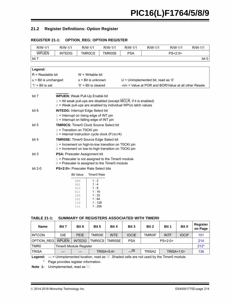
2014-2018 Microchip Technology Inc. DS40001775D-page 214
PIC16(L)F1764/5/8/9
21.2 Register Definitions: Option Register
TABLE 21-1: SUMMARY OF REGISTERS ASSOCIATED WITH TIMER0
REGISTER 21-1: OPTION_REG: OPTION REGISTER
R/W-1/1 R/W-1/1 R/W-1/1 R/W-1/1 R/W-1/1 R/W-1/1 R/W-1/1 R/W-1/1
WPUEN INTEDG TMR0CS TMR0SE PSA PS<2:0>
bit 7 bit 0
Legend:
R = Readable bit W = Writable bit
u = Bit is unchanged x = Bit is unknown U = Unimplemented bit, read as ‘0’
‘1’ = Bit is set ‘0’ = Bit is cleared -n/n = Value at POR and BOR/Value at all other Resets
bit 7 WPUEN: Weak Pull-Up Enable bit
1 = All weak pull-ups are disabled (except MCLR, if it is enabled)0 = Weak pull-ups are enabled by individual WPUx latch values
bit 6 INTEDG: Interrupt Edge Select bit
1 = Interrupt on rising edge of INT pin0 = Interrupt on falling edge of INT pin
bit 5 TMR0CS: Timer0 Clock Source Select bit
1 = Transition on T0CKI pin0 = Internal instruction cycle clock (FOSC/4)
bit 4 TMR0SE: Timer0 Source Edge Select bit
1 = Increment on high-to-low transition on T0CKI pin0 = Increment on low-to-high transition on T0CKI pin
bit 3 PSA: Prescaler Assignment bit
1 = Prescaler is not assigned to the Timer0 module0 = Prescaler is assigned to the Timer0 module
bit 2-0 PS<2:0>: Prescaler Rate Select bits
Name Bit 7 Bit 6 Bit 5 Bit 4 Bit 3 Bit 2 Bit 1 Bit 0Register on Page
INTCON GIE PEIE TMR0IE INTE IOCIE TMR0IF INTF IOCIF 101
OPTION_REG WPUEN INTEDG TMR0CS TMR0SE PSA PS<2:0> 214
TMR0 Timer0 Module Register 212*
TRISA — — TRISA<5:4> —(1) TRISA2 TRISA<1:0> 136
Legend: — = Unimplemented location, read as ‘0’. Shaded cells are not used by the Timer0 module.
* Page provides register information.
Note 1: Unimplemented, read as ‘1’.
000001010011100101110111
1 : 21 : 41 : 81 : 161 : 321 : 641 : 1281 : 256
Bit Value Timer0 Rate

2014-2018 Microchip Technology Inc. DS40001775D-page 215
PIC16(L)F1764/5/8/9
22.0 TIMER1/3/5 MODULE WITH GATE CONTROL
The Timer1 module is a 16-bit timer/counter with thefollowing features:
• 16-Bit Timer/Counter register pair (TMR1H:TMR1L)
• Programmable internal or external clock source
• 2-bit prescaler
• Dedicated 32 kHz oscillator circuit
• Optionally synchronized comparator out
• Multiple Timer1 gate (count enable) sources
• Interrupt-on-overflow
• Wake-up on overflow (external clock, Asynchronous mode only)
• Time base for the capture/compare function
• Auto-conversion trigger (with CCP)
• Selectable gate source polarity
• Gate Toggle mode
• Gate Single-Pulse mode
• Gate value status
• Gate event interrupt
Figure 22-1 is a block diagram of the Timer1 module.
This device has three instances of Timer1 typemodules. They include:
• Timer1
• Timer3
• Timer5
All references to Timer1 and Timer1 gate apply equallyto Timer3 and Timer5.
FIGURE 22-1: TIMER1 BLOCK DIAGRAM
TMR1H TMR1L
T1SYNC
T1CKPS<1:0>
Prescaler1, 2, 4, 8
0
1
SynchronizedClock Input
2
TMR1(2)
TMR1ON
Note 1: ST Buffer is high-speed type when using T1CKI.2: Timer1 register increments on rising edge.3: Synchronize does not operate while in Sleep.
T1G
SOSC
FOSC/4Internal
Clock
SOSCO
SOSCI
T1OSCEN
1
0
T1CKI
TMR1CS<1:0>
(1)
Synchronize(3)
det
Sleep input
TMR1GE
0
1
00
01
10
11
T1GPOL
D
QCK
Q
0
1
T1GVAL
T1GTM
T1GSPM
T1GGO/DONE
T1GSS<1:0>
EN
OUT
10
11
00
01FOSC
InternalClock
R
D
EN
Q
Q1RDT1GCON
Data Bus
TMR1GIF
Set
T1CLK
FOSC/2Internal
Clock
D
EN
Q
t1g_in
TMR1ON
LFINTOSC
Timer0 Overflow
sync_C2OUT
sync_C1OUT
To Comparator Module
To Clock Switching Modules
Set Flag bitTMR1IF onOverflow
To ADC Auto-Conversion
T1GPPS
PPS
T1CKIPPS
PPS
Interrupt
det
Single-Pulse
Acq. Control
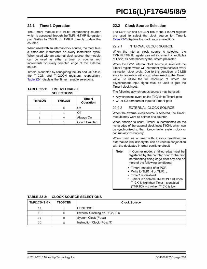
2014-2018 Microchip Technology Inc. DS40001775D-page 216
PIC16(L)F1764/5/8/9
22.1 Timer1 Operation
The Timer1 module is a 16-bit incrementing counterwhich is accessed through the TMR1H:TMR1L registerpair. Writes to TMR1H or TMR1L directly update thecounter.
When used with an internal clock source, the module isa timer and increments on every instruction cycle.When used with an external clock source, the modulecan be used as either a timer or counter andincrements on every selected edge of the externalsource.
Timer1 is enabled by configuring the ON and GE bits inthe T1CON and T1GCON registers, respectively.Table 22-1 displays the Timer1 enable selections.
22.2 Clock Source Selection
The CS<1:0> and OSCEN bits of the T1CON registerare used to select the clock source for Timer1.Table 22-2 displays the clock source selections.
22.2.1 INTERNAL CLOCK SOURCE
When the internal clock source is selected, theTMR1H:TMR1L register pair will increment on multiplesof FOSC, as determined by the Timer1 prescaler.
When the FOSC internal clock source is selected, theTimer1 register value will increment by four counts everyinstruction clock cycle. Due to this condition, a 2 LSBerror in resolution will occur when reading the Timer1value. To utilize the full resolution of Timer1, anasynchronous input signal must be used to gate theTimer1 clock input.
The following asynchronous sources may be used:
• Asynchronous event on the T1G pin to Timer1 gate• C1 or C2 comparator input to Timer1 gate
22.2.2 EXTERNAL CLOCK SOURCE
When the external clock source is selected, the Timer1module may work as a timer or a counter.
When enabled to count, Timer1 is incremented on therising edge of the external clock input T1CKI, which canbe synchronized to the microcontroller system clock orcan run asynchronously.
When used as a timer with a clock oscillator, anexternal 32.768 kHz crystal can be used in conjunctionwith the dedicated internal oscillator circuit.
TABLE 22-1: TIMER1 ENABLE SELECTIONS
TMR1ON TMR1GETimer1
Operation
0 0 Off
0 1 Off
1 0 Always On
1 1 Count Enabled
Note: In Counter mode, a falling edge must beregistered by the counter prior to the firstincrementing rising edge after any one ormore of the following conditions:
• Timer1 enabled after POR• Write to TMR1H or TMR1L• Timer1 is disabled• Timer1 is disabled (TMR1ON = 0) when
T1CKI is high then Timer1 is enabled (TMR1ON = 1) when T1CKI is low
TABLE 22-2: CLOCK SOURCE SELECTIONS
TMR1CS<1:0> T1OSCEN Clock Source
11 x LFINTOSC
10 0 External Clocking on T1CKI Pin
01 x System Clock (FOSC)
00 x Instruction Clock (FOSC/4)

2014-2018 Microchip Technology Inc. DS40001775D-page 217
PIC16(L)F1764/5/8/9
22.3 Timer1 Prescaler
Timer1 has four prescaler options, allowing 1, 2, 4 or 8divisions of the clock input. The CKPS<1:0> bits of theT1CON register control the prescale counter. Theprescale counter is not directly readable or writable;however, the prescaler counter is cleared upon a write toTMR1H or TMR1L.
22.4 Timer1 (Secondary) Oscillator
A dedicated low-power 32.768 kHz oscillator circuit isbuilt in between pins, SOSCI (input) and SOSCO(amplifier output). This internal circuit is to be used inconjunction with an external 32.768 kHz crystal.
The oscillator circuit is enabled by setting the OSCENbit of the T1CON register. The oscillator will continue torun during Sleep.
22.5 Timer1 Operation in Asynchronous Counter Mode
If the control bit, SYNC of the T1CON register, is set,the external clock input is not synchronized. The timerincrements asynchronously to the internal phaseclocks. If the external clock source is selected then thetimer will continue to run during Sleep and cangenerate an interrupt-on-overflow, which will wake-upthe processor. However, special precautions insoftware are needed to read/write the timer (seeSection 22.5.1 “Reading and Writing Timer1 inAsynchronous Counter Mode”).
22.5.1 READING AND WRITING TIMER1 IN ASYNCHRONOUS COUNTER MODE
Reading TMR1H or TMR1L while the timer is runningfrom an external asynchronous clock will ensure a validread (taken care of in hardware). However, the usershould keep in mind that reading the 16-bit timer in two8-bit values itself, poses certain problems, since thetimer may overflow between the reads.
For writes, it is recommended that the user simply stopthe timer and write the desired values. A writecontention may occur by writing to the timer registers,while the register is incrementing. This may produce anunpredictable value in the TMR1H:TMR1L register pair.
22.6 Timer1 Gate
Timer1 can be configured to count freely or the countcan be enabled and disabled using Timer1 gatecircuitry. This is also referred to as Timer1 Gate Enable.
Timer1 gate can also be driven by multiple selectablesources.
22.6.1 TIMER1 GATE ENABLE
The Timer1 Gate Enable mode is enabled by settingthe GE bit of the T1GCON register. The polarity of theTimer1 Gate Enable mode is configured using theGPOL bit of the T1GCON register.
When Timer1 Gate Enable mode is enabled, Timer1will increment on the rising edge of the Timer1 clocksource. When Timer1 Gate Enable mode is disabled,no incrementing will occur and Timer1 will hold thecurrent count. See Figure 22-3 for timing details.
Note: The oscillator requires a start-up andstabilization time before use. Thus,OSCEN should be set and a suitabledelay observed prior to using Timer1. Asuitable delay similar to the OST delaycan be implemented in software byclearing the TMR1IF bit then presettingthe TMR1H:TMR1L register pair toFC00h. The TMR1IF flag will be set when1024 clock cycles have elapsed, therebyindicating that the oscillator is running andreasonably stable.
Note: When switching from synchronous toasynchronous operation, it is possible toskip an increment. When switching fromasynchronous to synchronous operation,it is possible to produce an additionalincrement.
TABLE 22-3: TIMER1 GATE ENABLE SELECTIONS
T1CLK T1GPOL T1G Timer1 Operation
0 0 Counts
0 1 Holds Count
1 0 Holds Count
1 1 Counts

2014-2018 Microchip Technology Inc. DS40001775D-page 218
PIC16(L)F1764/5/8/9
22.6.2 TIMER1 GATE SOURCE SELECTION
Timer1 gate source selections are shown in Table 22-4.Source selection is controlled by the T1GSS bits of theT1GCON register. The polarity for each available sourceis also selectable. Polarity selection is controlled by theT1GPOL bit of the T1GCON register.
TABLE 22-4: TIMER1 GATE SOURCES
22.6.2.1 T1G Pin Gate Operation
The T1G pin is one source for Timer1 gate control. Itcan be used to supply an external source to the Timer1gate circuitry.
22.6.2.2 Timer0 Overflow Gate Operation
When Timer0 increments from FFh to 00h, alow-to-high pulse will automatically be generated andinternally supplied to the Timer1 gate circuitry.
22.6.2.3 Comparator C1 Gate Operation
The output resulting from a Comparator 1 operation canbe selected as a source for Timer1 gate control. TheComparator 1 output (sync_C1OUT) can besynchronized to the Timer1 clock or left asynchronous.For more information, see Section 19.4.1 “ComparatorOutput Synchronization”.
22.6.2.4 Comparator C2 Gate Operation
The output resulting from a Comparator 2 operationcan be selected as a source for Timer1 gate control.The Comparator 2 output (sync_C2OUT) can besynchronized to the Timer1 clock or left asynchronous.For more information, see Section 19.4.1 “ComparatorOutput Synchronization”.
22.6.3 TIMER1 GATE TOGGLE MODE
When Timer1 Gate Toggle mode is enabled, it ispossible to measure the full-cycle length of a Timer1gate signal, as opposed to the duration of a single levelpulse.
The Timer1 gate source is routed through a flip-flop thatchanges state on every incrementing edge of thesignal. See Figure 22-4 for timing details.
Timer1 Gate Toggle mode is enabled by setting theT1GTM bit of the T1GCON register. When the T1GTMbit is cleared, the flip-flop is cleared and held clear. Thisis necessary in order to control which edge ismeasured.
22.6.4 TIMER1 GATE SINGLE-PULSE MODE
When Timer1 Gate Single-Pulse mode is enabled, it ispossible to capture a single-pulse gate event. Timer1Gate Single-Pulse mode is first enabled by setting theT1GSPM bit in the T1GCON register. Next, theT1GGO/DONE bit in the T1GCON register must be set.The Timer1 will be fully enabled on the nextincrementing edge. On the next trailing edge of thepulse, the T1GGO/DONE bit will automatically becleared. No other gate events will be allowed toincrement Timer1 until the T1GGO/DONE bit is onceagain set in software. See Figure 22-5 for timing details.
If the Single-Pulse Gate mode is disabled by clearing theT1GSPM bit in the T1GCON register, the T1GGO/DONEbit should also be cleared.
Enabling the Toggle mode and the Single-Pulse modesimultaneously will permit both sections to worktogether. This allows the cycle times on the Timer1 gatesource to be measured. See Figure 22-6 for timingdetails.
22.6.5 TIMER1 GATE VALUE STATUS
When Timer1 gate value status is utilized, it is possibleto read the most current level of the gate control value.The value is stored in the T1GVAL bit in the T1GCONregister. The T1GVAL bit is valid even when the Timer1gate is not enabled (TMR1GE bit is cleared).
22.6.6 TIMER1 GATE EVENT INTERRUPT
When Timer1 Gate Event Interrupt is enabled, it ispossible to generate an interrupt upon the completionof a gate event. When the falling edge of T1GVALoccurs, the TMR1GIF flag bit in the PIR1 register will beset. If the TMR1GIE bit in the PIE1 register is set, thenan interrupt will be recognized.
The TMR1GIF flag bit operates even when the Timer1gate is not enabled (TMR1GE bit is cleared).
T1GSS<1:0> Timer1 Gate Source
00 Timer1 Gate Pin
01 Overflow of Timer0(TMR0 increments from FFh to 00h)
10 Comparator 1 Output sync_C1OUT(optionally Timer1 synchronized output)
11 Comparator 2 Output sync_C2OUT(optionally Timer1 synchronized output)
Note: Enabling Toggle mode at the same timeas changing the gate polarity may result inindeterminate operation.

2014-2018 Microchip Technology Inc. DS40001775D-page 219
PIC16(L)F1764/5/8/9
22.7 Timer1 Interrupt
The Timer1 register pair (TMR1H:TMR1L) incrementsto FFFFh and rolls over to 0000h. When Timer1 rollsover, the Timer1 interrupt flag bit of the PIR1 register isset. To enable the interrupt-on-rollover, you must setthese bits:
• ON bit of the T1CON register
• TMR1IE bit of the PIE1 register
• PEIE bit of the INTCON register
• GIE bit of the INTCON register
The interrupt is cleared by clearing the TMR1IF bit inthe Interrupt Service Routine.
22.8 Timer1 Operation During Sleep
Timer1 can only operate during Sleep when setup inAsynchronous Counter mode. In this mode, an externalcrystal or clock source can be used to increment thecounter. To set up the timer to wake the device:
• ON bit of the T1CON register must be set
• TMR1IE bit of the PIE1 register must be set
• PEIE bit of the INTCON register must be set
• SYNC bit of the T1CON register must be set
• CS<1:0> bits of the T1CON register must be configured
• OSCEN bit of the T1CON register must be configured
The device will wake-up on an overflow and executethe next instructions. If the GIE bit of the INTCONregister is set, the device will call the Interrupt ServiceRoutine.
The secondary oscillator will continue to operate inSleep regardless of the SYNC bit setting.
22.9 CCP Capture/Compare Time Base
The CCP modules use the TMR1H:TMR1L registerpair as the time base when operating in Capture orCompare mode.
In Capture mode, the value in the TMR1H:TMR1Lregister pair is copied into the CCPR1H:CCPR1Lregister pair on a configured event.
In Compare mode, an event is triggered when the valueCCPR1H:CCPR1L register pair matches the value inthe TMR1H:TMR1L register pair. This event can be anAuto-conversion Trigger.
For more information, see Section 24.0“Capture/Compare/PWM Modules”.
22.10 CCP Auto-Conversion Trigger
When any of the CCPs are configured to trigger anauto-conversion, the trigger will clear theTMR1H:TMR1L register pair. This auto-conversiondoes not cause a Timer1 interrupt. The CCP modulemay still be configured to generate a CCP interrupt.
In this mode of operation, the CCPR1H:CCPR1Lregister pair becomes the period register for Timer1.
Timer1 should be synchronized and FOSC/4 should beselected as the clock source in order to utilize theAuto-conversion Trigger. Asynchronous operation ofTimer1 can cause an Auto-conversion Trigger to bemissed.
In the event that a write to TMR1H or TMR1L coincideswith an Auto-conversion Trigger from the CCP, thewrite will take precedence.
For more information, see Section 24.2.1“Auto-Conversion Trigger”.
FIGURE 22-2: TIMER1 INCREMENTING EDGE
Note: The TMR1H:TMR1L register pair and theTMR1IF bit should be cleared beforeenabling interrupts.
T1CKI = 1when TMR1Enabled
T1CKI = 0when TMR1Enabled
Note 1: Arrows indicate counter increments.2: In Counter mode, a falling edge must be registered by the counter prior to the first incrementing rising edge
of the clock.

2014-2018 Microchip Technology Inc. DS40001775D-page 220
PIC16(L)F1764/5/8/9
FIGURE 22-3: TIMER1 GATE ENABLE MODE
FIGURE 22-4: TIMER1 GATE TOGGLE MODE
TMR1GE
T1GPOL
t1g_in
T1CKI
T1GVAL
Timer1 N N + 1 N + 2 N + 3 N + 4
TMR1GE
T1GPOL
T1GTM
t1g_in
T1CKI
T1GVAL
Timer1 N N + 1 N + 2 N + 3 N + 4 N + 5 N + 6 N + 7 N + 8

2014-2018 Microchip Technology Inc. DS40001775D-page 221
PIC16(L)F1764/5/8/9
FIGURE 22-5: TIMER1 GATE SINGLE-PULSE MODE
TMR1GE
T1GPOL
t1g_in
T1CKI
T1GVAL
Timer1 N N + 1 N + 2
T1GSPM
T1GGO/
DONE
Set by SoftwareCleared by Hardware onFalling Edge of T1GVAL
Set by Hardware onFalling Edge of T1GVAL
Cleared by SoftwareCleared bySoftwareTMR1GIF
Counting Enabled onRising Edge of T1G

2014-2018 Microchip Technology Inc. DS40001775D-page 222
PIC16(L)F1764/5/8/9
FIGURE 22-6: TIMER1 GATE SINGLE-PULSE AND TOGGLE COMBINED MODE
TMR1GE
T1GPOL
t1g_in
T1CKI
T1GVAL
Timer1 N N + 1 N + 2
T1GSPM
T1GGO/
DONE
Set by SoftwareCleared by Hardware onFalling Edge of T1GVAL
Set by Hardware onFalling Edge of T1GVALCleared by Software
Cleared bySoftwareTMR1GIF
T1GTM
Counting Enabled onRising Edge of T1G
N + 4N + 3
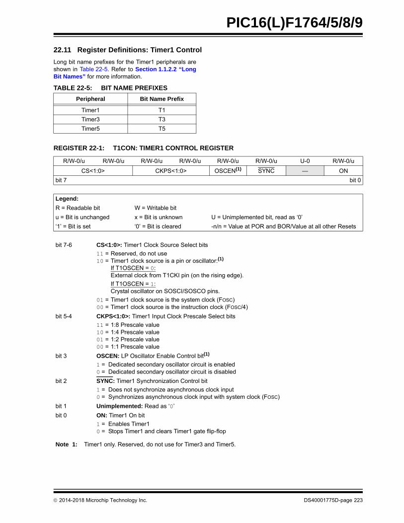
2014-2018 Microchip Technology Inc. DS40001775D-page 223
PIC16(L)F1764/5/8/9
22.11 Register Definitions: Timer1 Control
Long bit name prefixes for the Timer1 peripherals areshown in Table 22-5. Refer to Section 1.1.2.2 “LongBit Names” for more information.
TABLE 22-5: BIT NAME PREFIXES
Peripheral Bit Name Prefix
Timer1 T1
Timer3 T3
Timer5 T5
REGISTER 22-1: T1CON: TIMER1 CONTROL REGISTER
R/W-0/u R/W-0/u R/W-0/u R/W-0/u R/W-0/u R/W-0/u U-0 R/W-0/u
CS<1:0> CKPS<1:0> OSCEN(1) SYNC — ON
bit 7 bit 0
Legend:
R = Readable bit W = Writable bit
u = Bit is unchanged x = Bit is unknown U = Unimplemented bit, read as ‘0’
‘1’ = Bit is set ‘0’ = Bit is cleared -n/n = Value at POR and BOR/Value at all other Resets
bit 7-6 CS<1:0>: Timer1 Clock Source Select bits
11 = Reserved, do not use10 = Timer1 clock source is a pin or oscillator:(1)
If T1OSCEN = 0:External clock from T1CKI pin (on the rising edge).
If T1OSCEN = 1:Crystal oscillator on SOSCI/SOSCO pins.
01 = Timer1 clock source is the system clock (FOSC)00 = Timer1 clock source is the instruction clock (FOSC/4)
bit 5-4 CKPS<1:0>: Timer1 Input Clock Prescale Select bits
11 = 1:8 Prescale value10 = 1:4 Prescale value01 = 1:2 Prescale value00 = 1:1 Prescale value
bit 3 OSCEN: LP Oscillator Enable Control bit(1)
1 = Dedicated secondary oscillator circuit is enabled0 = Dedicated secondary oscillator circuit is disabled
bit 2 SYNC: Timer1 Synchronization Control bit
1 = Does not synchronize asynchronous clock input0 = Synchronizes asynchronous clock input with system clock (FOSC)
bit 1 Unimplemented: Read as ‘0’
bit 0 ON: Timer1 On bit
1 = Enables Timer10 = Stops Timer1 and clears Timer1 gate flip-flop
Note 1: Timer1 only. Reserved, do not use for Timer3 and Timer5.
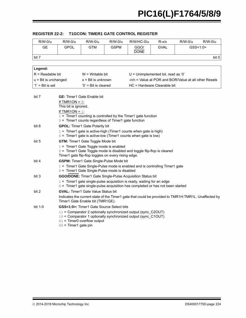
2014-2018 Microchip Technology Inc. DS40001775D-page 224
PIC16(L)F1764/5/8/9
REGISTER 22-2: T1GCON: TIMER1 GATE CONTROL REGISTER
R/W-0/u R/W-0/u R/W-0/u R/W-0/u R/W/HC-0/u R-x/x R/W-0/u R/W-0/u
GE GPOL GTM GSPM GGO/DONE
GVAL GSS<1:0>
bit 7 bit 0
Legend:
R = Readable bit W = Writable bit U = Unimplemented bit, read as ‘0’
u = Bit is unchanged x = Bit is unknown -n/n = Value at POR and BOR/Value at all other Resets
‘1’ = Bit is set ‘0’ = Bit is cleared HC = Hardware Clearable bit
bit 7 GE: Timer1 Gate Enable bit
If TMR1ON = 0:This bit is ignored.
If TMR1ON = 1:1 = Timer1 counting is controlled by the Timer1 gate function0 = Timer1 counts regardless of Timer1 gate function
bit 6 GPOL: Timer1 Gate Polarity bit
1 = Timer1 gate is active-high (Timer1 counts when gate is high)0 = Timer1 gate is active-low (Timer1 counts when gate is low)
bit 5 GTM: Timer1 Gate Toggle Mode bit
1 = Timer1 Gate Toggle mode is enabled0 = Timer1 Gate Toggle mode is disabled and toggle flip-flop is clearedTimer1 gate flip-flop toggles on every rising edge.
bit 4 GSPM: Timer1 Gate Single-Pulse Mode bit
1 = Timer1 Gate Single-Pulse mode is enabled and is controlling Timer1 gate0 = Timer1 Gate Single-Pulse mode is disabled
bit 3 GGO/DONE: Timer1 Gate Single-Pulse Acquisition Status bit
1 = Timer1 gate single-pulse acquisition is ready, waiting for an edge0 = Timer1 gate single-pulse acquisition has completed or has not been started
bit 2 GVAL: Timer1 Gate Value Status bit
Indicates the current state of the Timer1 gate that could be provided to TMR1H:TMR1L. Unaffected byTimer1 Gate Enable bit (TMR1GE).
bit 1-0 GSS<1:0>: Timer1 Gate Source Select bits
11 = Comparator 2 optionally synchronized output (sync_C2OUT)10 = Comparator 1 optionally synchronized output (sync_C1OUT)01 = Timer0 overflow output00 = Timer1 gate pin

2014-2018 Microchip Technology Inc. DS40001775D-page 225
PIC16(L)F1764/5/8/9
TABLE 22-6: SUMMARY OF REGISTERS ASSOCIATED WITH TIMER1
Name Bit 7 Bit 6 Bit 5 Bit 4 Bit 3 Bit 2 Bit 1 Bit 0Register on Page
ANSELA — — — ANSA4 — ANSA<2:0> 137
CCPxCON EN OE OUT FMT MODE<3:0> 256
INTCON GIE PEIE TMR0IE INTE IOCIE TMR0IF INTF IOCIF 101
PIE1 TMR1GIE ADIE RCIE TXIE SSP1IE CCP1IE TMR2IE TMR1IE 102
PIR1 TMR1GIF ADIF RCIF TXIF SSP1IF CCP1IF TMR2IF TMR1IF 105
TMRxH Holding Register for the Most Significant Byte of the 16-bit TMR1/3/5 Register 215*
TMRxL Holding Register for the Least Significant Byte of the 16-bit TMR1/3/5 Register 215*
TRISA — — TRISA<5:4> —(1) TRISA<2:0> 136
TxCON CS<1:0> CKPS<1:0> OSCEN SYNC — ON 223
TxGCON GE GPOL GTM GSPM GGO/DONE
GVAL GSS<1:0> 224
Legend: — = unimplemented location, read as ‘0’. Shaded cells are not used by the Timer1 module.
* Page provides register information.
Note 1: Unimplemented, read as ‘1’.
2: PIC16(L)F1768/9 only.

2014-2018 Microchip Technology Inc. DS40001775D-page 226
PIC16(L)F1764/5/8/9
23.0 TIMER2/4/6 MODULE
The Timer2/4/6 modules are 8-bit timers that can oper-ate as free-running period counters or in conjunctionwith external signals that control Start, Run, Freeze andReset operation in One-Shot and Monostable modes ofoperation. Sophisticated waveform control, such aspulse density modulation, are possible by combiningthe operation of these timers with other internal periph-erals, such as the comparators and CCP modules.Features of the timer include:
• 8-Bit Timer register
• 8-Bit Period register
• Selectable external hardware timer Resets
• Programmable prescaler (1:1 to 1:128)
• Programmable postscaler (1:1 to 1:16)
• Selectable synchronous/asynchronous operation
• Alternate clock sources
• Interrupt-on-period
• Three modes of operation:
- Free-Running Period
- One-Shot
- Monostable
See Figure 23-1 for a block diagram of Timer2. SeeFigure 23-2 for the clock source block diagram.
FIGURE 23-1: TIMER2 BLOCK DIAGRAM
Note: Three identical Timer2 modules areimplemented on this device. The timers arenamed Timer2, Timer4 and Timer6. Allreferences to Timer2 apply as well toTimer4 and Timer6. All references to T2PRapply as well to T4PR and T6PR.
Rev. 10-000 168B5/29/201 4
MODE<3>
Clear ON
TMRx
Comparator
PRx
CKSYNC
ON
OUTPS<3:0>
Postscaler
Set flag bi t TMRxIF
TMRx_postscaled
CKPOL
4
MODE<4:0>
PSYNC
Prescaler
CKPS<2:0>
3
TMRx_clk
RSEL
R
Sync (2 Clocks)
Edge DetectorLevel DetectorMode Control(2 clock Sync)
TMRx_ers
0
1
1
0
Note 1: Signal to the CCP to trigger the PWM pulse 2: See Section 22.5 for description of CCP interaction in the different TMR modes
enable
reset
Sync
Fosc/4
D Q
CCP_pset
MODE<4:1>=1011MODE<4:3>=01
PPSTxINPPSTxIN
External Reset Sources (Table 23-4)
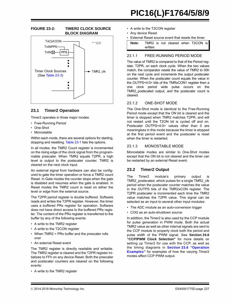
2014-2018 Microchip Technology Inc. DS40001775D-page 227
PIC16(L)F1764/5/8/9
FIGURE 23-2: TIMER2 CLOCK SOURCE BLOCK DIAGRAM
23.1 Timer2 Operation
Timer2 operates in three major modes:
• Free-Running Period• One-Shot• Monostable
Within each mode, there are several options for starting,stopping and resetting. Table 23-1 lists the options.
In all modes, the TMR2 Count register is incrementedon the rising edge of the clock signal from the program-mable prescaler. When TMR2 equals T2PR, a highlevel is output to the postscaler counter. TMR2 iscleared on the next clock input.
An external signal from hardware can also be config-ured to gate the timer operation or force a TMR2 countReset. In Gate modes the counter stops when the gateis disabled and resumes when the gate is enabled. InReset modes the TMR2 count is reset on either thelevel or edge from the external source.
The T2PR period register is double buffered. Softwarereads and writes the T2PR register. However, the timeruses a buffered PRx register for operation. Softwaredoes not have direct access to the buffered PRx regis-ter. The content of the PRx register is transferred to thebuffer by any of the following events:
• A write to the TMR2 register
• A write to the T2CON register
• When TMR2 = PRx buffer and the prescaler rolls over
• An external Reset event
The TMR2 register is directly readable and writable.The TMR2 register is cleared and the T2PR register ini-tializes to FFh on any device Reset. Both the prescalerand postscaler counters are cleared on the followingevents:
• A write to the TMR2 register
• A write to the T2CON register• Any device Reset• External Reset source event that resets the timer.
23.1.1 FREE-RUNNING PERIOD MODE
The value of TMR2 is compared to that of the Period reg-ister, T2PR, on each clock cycle. When the two valuesmatch, the comparator resets the value of TMR2 to 00hon the next cycle and increments the output postscalercounter. When the postscaler count equals the value inthe OUTPS<4:0> bits of the TMRxCON1 register then aone clock period wide pulse occurs on theTMR2_postscaled output, and the postscaler count iscleared.
23.1.2 ONE-SHOT MODE
The One-Shot mode is identical to the Free-RunningPeriod mode except that the ON bit is cleared and thetimer is stopped when TMR2 matches T2PR, and willnot restart until the T2ON bit is cycled off and on.Postscaler OUTPS<4:0> values other than 0 aremeaningless in this mode because the timer is stoppedat the first period event and the postscaler is resetwhen the timer is restarted.
23.1.3 MONOSTABLE MODE
Monostable modes are similar to One-Shot modesexcept that the ON bit is not cleared and the timer canbe restarted by an external Reset event.
23.2 Timer2 Output
The Timer2 module’s primary output isTMR2_postscaled, which pulses for a single TMR2_clkperiod when the postscaler counter matches the valuein the OUTPS bits of the TMR2xCON register. TheT2PR postscaler is incremented each time the TMR2value matches the T2PR value. This signal can beselected as an input to several other input modules:
• The ADC module as an auto-conversion trigger
• COG as an auto-shutdown source
In addition, the Timer2 is also used by the CCP modulefor pulse generation in PWM mode. Both the actualTMR2 value as well as other internal signals are sent tothe CCP module to properly clock both the period andpulse width of the PWM signal. See Section 24.6“CCP/PWM Clock Selection” for more details onsetting up Timer2 for use with the CCP, as well asthe timing diagrams in Section 23.6 “OperationExamples” for examples of how the varying Timer2modes affect CCP PWM output.
Rev. 10-000 169B5/29/201 4
TMR2_clk
TXIN
TxCLKCON
PPS
TXINPPS
Timer Clock Sources (See Table 23-3)
Note: TMR2 is not cleared when T2CON iswritten.

2014-2018 Microchip Technology Inc. DS40001775D-page 228
PIC16(L)F1764/5/8/9
23.3 External Reset Sources
In addition to the clock source, the Timer2 also takes inan external Reset source. This external Reset sourceis selected for Timer2, Timer4 and Timer6, with theT2RST, T4RST and T6RST registers, respectively.This source can control starting and stopping of thetimer, as well as resetting the timer, depending onwhich mode the timer is in. The mode of the timer is
controlled by the MODE<4:0> bits of the TMRxHLTregister. Edge-Triggered modes require six timer clockperiods between external triggers. Level-Triggeredmodes require the triggering level to be at least threetimer clock periods long. External triggers are ignoredwhile in Debug Freeze mode.
23.4 Operating Modes
TABLE 23-1: TIMER2 OPERATING MODES
ModeMODE<4:0> Output
OperationOperation
Timer Control
<4:3> <2:0> Start Reset Stop
Free-Running Period
00
000
Period Pulse
Software gate (Figure 23-4) ON = 1 — ON = 0
001Hardware gate, active-high
(Figure 23-5)ON = 1 and
TMRx_ers = 1—
ON = 0 orTMRx_ers = 0
010Hardware gate, active-low ON = 1 and
TMRx_ers = 0—
ON = 0 orTMRx_ers = 1
011
PeriodPulse with
HardwareReset
Rising or falling edge Reset
ON = 1
TMRx_ers ↕
ON = 0100 Rising edge Reset (Figure 23-6) TMRx_ers ↑
101 Falling edge Reset TMRx_ers ↓
110 Low-level Reset TMRx_ers = 0ON = 0 or
TMRx_ers = 0
111 High-level Reset (Figure 23-7) TMRx_ers = 1ON = 0 or
TMRx_ers = 1
One-Shot 01
000 One-Shot Software start (Figure 23-8) ON = 1 —
ON = 0or
next clock after TMRx = PRx
(Note 2)
001Edge-
Triggered Start
(Note 1)
Rising edge start (Figure 23-9)ON = 1 andTMRx_ers ↑
—
010 Falling edge startON = 1 andTMRx_ers ↓
—
011 Any edge startON = 1 andTMRx_ers ↕
—
100Edge-
Triggered Startand
Hardware Reset
(Note 1)
Rising edge start andrising edge Reset (Figure 23-10)
ON = 1 andTMRx_ers ↑
TMRx_ers ↑
101Falling edge start and
falling edge ResetON = 1 andTMRx_ers ↓
TMRx_ers ↓
110Rising edge start and
low-level Reset (Figure 23-11)ON = 1 andTMRx_ers ↑
TMRx_ers = 0
111Falling edge start and
high-level ResetON = 1 andTMRx_ers ↓
TMRx_ers = 1
Mono-stable
10
000 Reserved
001Edge-
TriggeredStart
(Note 1)
Rising edge start(Figure 23-12)
ON = 1 andTMRx_ers ↑
— ON = 0or
next clock after TMRx = PRx
(Note 3)
010 Falling edge startON = 1 andTMRx_ers ↓
—
011 Any edge startON = 1 andTMRx_ers ↕
—
Reserved 100 Reserved
Reserved 101 Reserved
One-shot
110Level-
TriggeredStartand
Hardware Reset
High-level start andlow-level Reset (Figure 23-13)
ON = 1 andTMRx_ers = 1
TMRx_ers = 0ON = 0 or
held in Reset(Note 2)111
Low-level start andhigh-level Reset
ON = 1 andTMRx_ers = 0
TMRx_ers = 1
Reserved 11 xxx Reserved

2014-2018 Microchip Technology Inc. DS40001775D-page 229
PIC16(L)F1764/5/8/9
Note 1: If ON = 0, then an edge is required to restart the timer after ON = 1.
2: When TMRx = PRx, then the next clock clears ON and stops TMRx at 00h.
3: When TMRx = PRx, then the next clock stops TMRx at 00h but does not clear ON.
TABLE 23-1: TIMER2 OPERATING MODES
ModeMODE<4:0> Output
OperationOperation
Timer Control
<4:3> <2:0> Start Reset Stop

2014-2018 Microchip Technology Inc. DS40001775D-page 230
PIC16(L)F1764/5/8/9
23.5 Timer2 Interrupt
Timer2 can also generate a device interrupt. Theinterrupt is generated when the postscaler countermatches one of 16 postscale options (from 1:1 through1:16), which are selected with the postscaler controlbits, OUTPS<3:0> of the T2CON register. The interruptis enabled by setting the TMR2IE interrupt enable bit ofthe PIE1 register. Interrupt timing is illustrated inFigure 23-3.
FIGURE 23-3: TIMER2 PRESCALER, POSTSCALER AND INTERRUPT TIMING DIAGRAM
Rev. 10-000205A4/7/2016
TMRx_clk
PRx
TMRx
1
0
CKPS 0b010
TMRx_postscaled
OUTPS 0b0001
1 0 1 0 1 0
TMRxIF (1)(1) (2)

2014-2018 Microchip Technology Inc. DS40001775D-page 231
PIC16(L)F1764/5/8/9
23.6 Operation Examples
Unless otherwise specified, the following notes apply tothe following timing diagrams:
- Both the prescaler and postscaler are set to 1:1 (both the CKPSx and OUTPSx bits in the TxCON register are cleared).
- The diagrams illustrate any clock except FOSC/4 and show clock-sync delays of at least two full cycles for both ON and Timer2_ers. When using FOSC/4, the clock-sync delay is at least one instruction period for Timer2_ers; ON applies in the next instruction period.
- The PWM duty cycle and PWM output are illustrated assuming that the timer is used for the PWM function of the CCP module, as described in Section 24.6 “CCP/PWM Clock Selection”. The signals are not a part of the Timer2 module.
23.6.1 SOFTWARE GATE MODE
This mode corresponds to legacy Timer2 operation.The timer increments with each clock input whenON = 1 and does not increment when ON = 0. Whenthe TMRx count equals the PRx period count, the timerresets on the next clock and continues counting from 0.Operation with the ON bit software controlled is illus-trated in Figure 23-4. With PRx = 5, the counteradvances until TMRx = 5, and goes to zero with thenext clock.
FIGURE 23-4: SOFTWARE GATE MODE TIMING DIAGRAM (MODE<4:0> = 00000)
Rev. 10-000195B5/30/2014
TMRx_clk
Instruction(1)
ON
PRx
TMRx
TMRx_postscaled
BSF BCF BSF
5
0 1 2 3 4 5 0 1 2 2 3 4 5
MODE 0b00000
3 4 5 0 1 0 1
PWM Duty Cycle 3
PWM Output
Note 1: BSF and BCF represent Bit-Set File and Bit-Clear File instructions executed by the CPU to set or clear the ON bit of TxCON. CPU execution is asynchronous to the timer clock input.

2014-2018 Microchip Technology Inc. DS40001775D-page 232
PIC16(L)F1764/5/8/9
23.6.2 HARDWARE GATE MODE
The Hardware Gate modes operate the same as theSoftware Gate mode, except the TMRx_ers externalsignal can also gate the timer. When used with theCCP, the gating extends the PWM period. If the timer isstopped when the PWM output is high, then the dutycycle is also extended.
When MODE<4:0> = 00001, then the timer is stoppedwhen the external signal is high. WhenMODE<4:0> = 00010, then the timer is stopped whenthe external signal is low.
Figure 23-5 illustrates the Hardware Gating mode forMODE<4:0> = 00001 in which a high input level startsthe counter.
FIGURE 23-5: HARDWARE GATE MODE TIMING DIAGRAM (MODE<4:0> = 00001)
Rev. 10-000 196B5/30/201 4
TMRx_clk
TMRx_ers
PRx
TMRx
TMRx_postscaled
5
MODE 0b00001
0 1 2 3 4 5 0 1 2 3 4 5 0 1
PWM Duty Cycle 3
PWM Output

2014-2018 Microchip Technology Inc. DS40001775D-page 233
PIC16(L)F1764/5/8/9
23.6.3 EDGE-TRIGGERED HARDWARE LIMIT MODE
In Hardware Limit mode, the timer can be reset by theTMRx_ers external signal before the timer reaches theperiod count. Three types of Resets are possible:
• Reset on rising or falling edge (MODE<4:0>= 00011)
• Reset on rising edge (MODE<4:0> = 00100)
• Reset on falling edge (MODE<4:0> = 00101)
When the timer is used in conjunction with the CCP inPWM mode, then an early Reset shortens the periodand restarts the PWM pulse after a two-clock delay.Refer to Figure 23-6.
FIGURE 23-6: EDGE-TRIGGERED HARDWARE LIMIT MODE TIMING DIAGRAM (MODE<4:0> = 00100)
Rev. 10-000 197B5/30/201 4
TMRx_clk
ON
PRx
TMRx
BSF BCF BSF
5
0 1 2 0 1 2 3 4 5 0 4 5 0
MODE 0b00100
TMRx_ers
1 2 3 1
TMRx_postscaled
PWM Duty Cycle 3
PWM Output
Instruction(1)
Note 1: BSF and BCF represent Bit-Set File and Bit-Clear File instructions executed by the CPU to set or clear the ON bit of TxCON. CPU execution is asynchronous to the timer clock input.

2014-2018 Microchip Technology Inc. DS40001775D-page 234
PIC16(L)F1764/5/8/9
23.6.4 LEVEL-TRIGGERED HARDWARE LIMIT MODE
In the Level-Triggered Hardware Limit Timer modes,the counter is reset by high or low levels of the externalsignal, TMRx_ers, as shown in Figure 23-7. SelectingMODE<4:0> = 00110 will cause the timer to reset on alow-level external signal. Selecting MODE<4:0> = 00111will cause the timer to reset on a high-level externalsignal. In the example, the counter is reset whileTMRx_ers = 1. ON is controlled by BSF and BCFinstructions. When ON = 0, the external signal isignored.
When the CCP uses the timer as the PWM time base,then the PWM output will be set high when the timerstarts counting and then set low only when the timercount matches the CCPRx value. The timer is resetwhen either the timer count matches the PRx value ortwo clock periods after the external Reset signal goestrue and stays true.
The timer starts counting, and the PWM output is sethigh, on either the clock following the PRx match or twoclocks after the external Reset signal relinquishes theReset. The PWM output will remain high until the timercounts up to match the CCPRx pulse-width value. If theexternal Reset signal goes true while the PWM outputis high then the PWM output will remain high until theReset signal is released allowing the timer to count upto match the CCPRx value.
FIGURE 23-7: LEVEL-TRIGGERED HARDWARE LIMIT MODE TIMING DIAGRAM(MODE<4:0> = 00111)
Rev. 10-000198B5/30/2014
TMRx_clk
ON
PRx
TMRx
BSF BCF BSF
5
0 1 2 0 1 2 3 4 5 1 2 3
MODE 0b00111
TMRx_ers
0 0 4
TMRx_postscaled
5 0
PWM Duty Cycle 3
PWM Output
Instruction(1)
Note 1: BSF and BCF represent Bit-Set File and Bit-Clear File instructions executed by the CPU to set or clear the ON bit of TxCON. CPU execution is asynchronous to the timer clock input.

2014-2018 Microchip Technology Inc. DS40001775D-page 235
PIC16(L)F1764/5/8/9
23.6.5 SOFTWARE START ONE-SHOT MODE
In One-Shot mode, the timer resets and the ON bit iscleared when the timer value matches the PRx periodvalue. The ON bit must be set by software to startanother timer cycle. Setting MODE<4:0> = 01000selects One-Shot mode, which is illustrated inFigure 23-8. In the example, ON is controlled by theBSF and BCF instructions. In the first case, a BSFinstruction sets ON and the counter runs to completionand clears ON. In the second case, a BSF instructionstarts the cycle, BCF/BSF instructions turn the counteroff and on during the cycle, and then it runs tocompletion.
When One-Shot mode is used in conjunction with theCCP PWM operation, the PWM pulse drive starts con-current with setting the ON bit. Clearing the ON bitwhile the PWM drive is active will extend the PWMdrive. The PWM drive will terminate when the timervalue matches the CCPRx pulse-width value. ThePWM drive will remain off until software sets the ON bitto start another cycle. If software clears the ON bit afterthe CCPRx match, but before the PRx match, then thePWM drive will be extended by the length of time theON bit remains cleared. Another timing cycle can onlybe initiated by setting the ON bit after it has beencleared by a PRx period count match.
FIGURE 23-8: SOFTWARE START ONE-SHOT MODE TIMING DIAGRAM (MODE<4:0> = 01000)
Rev. 10-000199B4/7/2016
TMRx_clk
ON
PRx
TMRx
BSF BSF
5
0 1 2 3 4 5 0 431
MODE 0b01000
2 5 0
TMRx_postscaled
BCF BSF
PWM Duty Cycle 3
PWM Output
Note 1: BSF and BCF represent Bit-Set File and Bit-Clear File instructions executed by the CPU to set or clear the ON bit of TxCON. CPU execution is asynchronous to the timer clock input.
Instruction(1)

2014-2018 Microchip Technology Inc. DS40001775D-page 236
PIC16(L)F1764/5/8/9
23.6.6 EDGE-TRIGGERED ONE-SHOT MODE
The Edge-Triggered One-Shot modes start the timer on an edge from the external signal input, after the ON bit is set, and clear the ON bit when the timer matches the PRx period value. The following edges will start the timer:• Rising edge (MODE<4:0> = 01001)
• Falling edge (MODE<4:0> = 01010)
• Rising or falling edge (MODE<4:0> = 01011)
If the timer is halted by clearing the ON bit, then anotherTMRx_ers edge is required after the ON bit is set toresume counting. Figure 23-9 illustrates operation inthe rising edge One-Shot mode.
When Edge-Triggered One-Shot mode is used inconjunction with the CCP, then the edge-trigger willactivate the PWM drive and the PWM drive willdeactivate when the timer matches the CCPRxpulse-width value and stay deactivated when the timerhalts at the PRx period count match.
FIGURE 23-9: EDGE-TRIGGERED ONE-SHOT MODE TIMING DIAGRAM (MODE<4:0> = 01001)Rev. 10-000200B
5/19/2016
TMRx_clk
ON
PRx
TMRx
BSF BSF
5
0 1 2 3 4 5 0 1
MODE 0b01001
2
CCP_pset
TMRx_postscaled
BCF
TMRx_ers
PWM Duty Cycle 3
PWM Output
Instruction(1)
Note 1: BSF and BCF represent Bit-Set File and Bit-Clear File instructions executed by the CPU to set or clear the ON bit of TxCON. CPU execution is asynchronous to the timer clock input.

2014-2018 Microchip Technology Inc. DS40001775D-page 237
PIC16(L)F1764/5/8/9
23.6.7 EDGE-TRIGGERED HARDWARE LIMIT ONE-SHOT MODE
In Edge-Triggered Hardware Limit One-Shot modes,the timer starts on the first external signal edge after theON bit is set and resets on all subsequent edges. Onlythe first edge after the ON bit is set is needed to startthe timer. The counter will resume counting automati-cally, two clocks after all subsequent external Resetedges. Edge triggers are as follows:
• Rising edge start and Reset (MODE<4:0> = 01100)
• Falling edge start and Reset (MODE<4:0> = 01101)
The timer resets and clears the ON bit when the timervalue matches the PRx period value. External signaledges will have no effect until after software sets theON bit. Figure 23-10 illustrates the rising edge hard-ware limit one-shot operation.
When this mode is used in conjunction with the CCPthen the first starting edge trigger, and all subsequentReset edges, will activate the PWM drive. The PWMdrive will deactivate when the timer matches theCCPRx pulse-width value and stay deactivated untilthe timer halts at the PRx period match unless an exter-nal signal edge resets the timer before the matchoccurs.
FIGURE 23-10: EDGE-TRIGGERED HARDWARE LIMIT ONE-SHOT MODE TIMING DIAGRAM (MODE<4:0> = 01100)
Rev. 10-000201B4/7/2016
TMRx_clk
ON
PRx
TMRx
BSF BSF
5
0 1 2 3 4 5 0 01
MODE 0b01100
2
TMRx_postscaled
TMRx_ers
1 2 3 4 5 0
PWM Duty Cycle 3
PWM Output
Instruction(1)
Note 1: BSF and BCF represent Bit-Set File and Bit-Clear File instructions executed by the CPU to set or clear the ON bit of TxCON. CPU execution is asynchronous to the timer clock input.

2014-2018 Microchip Technology Inc. DS40001775D-page 238
PIC16(L)F1764/5/8/9
23.6.8 LEVEL RESET, EDGE-TRIGGERED HARDWARE LIMIT ONE-SHOT MODES
In Level-Triggered One-Shot mode, the timer count isreset on the external signal level and starts counting onthe rising/falling edge of the transition from Reset levelto the active level while the ON bit is set. Reset levelsare selected as follows:
• Low Reset level (MODE<4:0> = 01110)
• High Reset level (MODE<4:0> = 01111)
When the timer count matches the PRx period count,the timer is reset and the ON bit is cleared. When theON bit is cleared by either a PRx match or by softwarecontrol, a new external signal edge is required after theON bit is set to start the counter.
When Level-Triggered Reset One-Shot mode is usedin conjunction with the CCP PWM operation, the PWMdrive goes active with the external signal edge thatstarts the timer. The PWM drive goes inactive when thetimer count equals the CCPRx pulse-width count. ThePWM drive does not go active when the timer countclears at the PRx period count match.
FIGURE 23-11: LOW-LEVEL RESET, EDGE-TRIGGERED HARDWARE LIMIT ONE-SHOT MODE TIMING DIAGRAM (MODE<4:0> = 01110)
Rev. 10-000202B4/7/2016
TMRx_clk
ON
PRx
TMRx
BSF BSF
5
0 1 2 3 4 5 0 01
MODE 0b01110
TMRx_postscaled
TMRx_ers
1 2 3 4 0
PWM Duty Cycle 3
PWM Output
5
Instruction(1)
Note 1: BSF and BCF represent Bit-Set File and Bit-Clear File instructions executed by the CPU to set or clear the ON bit of TxCON. CPU execution is asynchronous to the timer clock input.

2014-2018 Microchip Technology Inc. DS40001775D-page 239
PIC16(L)F1764/5/8/9
23.6.9 EDGE-TRIGGERED MONOSTABLE MODES
The Edge-Triggered Monostable modes start the timeron an edge from the external Reset signal input, afterthe ON bit is set, and stop incrementing the timer whenthe timer matches the PRx period value. The followingedges will start the timer:
• Rising edge (MODE<4:0> = 10001)
• Falling edge (MODE<4:0> = 10010)
• Rising or falling edge (MODE<4:0> = 10011)
When an Edge-Triggered Monostable mode is used inconjunction with the CCP PWM operation, the PWMdrive goes active with the external Reset signal edgethat starts the timer, but will not go active when thetimer matches the PRx value. While the timer is incre-menting, additional edges on the external Reset signalwill not affect the CCP PWM.
FIGURE 23-12: RISING EDGE-TRIGGERED MONOSTABLE MODE TIMING DIAGRAM (MODE<4:0> = 10001)
Rev. 10-000203A4/7/2016
TMRx_clk
ON
PRx
TMRx
BSF BCF
5
0 1 2 3 4 5 0 1
MODE 0b10001
TMRx_postscaled
TMRx_ers
2 3 4 5 0
PWM Duty Cycle 3
PWM Output
Instruction(1)
Note 1: BSF and BCF represent Bit-Set File and Bit-Clear File instructions executed by the CPU to set or clear the ON bit of TxCON. CPU execution is asynchronous to the timer clock input.
BSF BCF BSF
1 2 3 4 5 0

2014-2018 Microchip Technology Inc. DS40001775D-page 240
PIC16(L)F1764/5/8/9
23.6.10 LEVEL-TRIGGERED HARDWARE LIMIT ONE-SHOT MODES
The Level-Triggered Hardware Limit One-Shot modeshold the timer in Reset on an external Reset level, andstart counting when both the ON bit is set and the exter-nal signal is not at the Reset level. If one of either of theexternal signals is not in Reset, or the ON bit is set,then the other signal being set/made active will start thetimer. Reset levels are selected as follows:
• Low Reset level (MODE<4:0> = 10110)
• High Reset level (MODE<4:0> = 10111)
When the timer count matches the PRx period count,the timer is reset and the ON bit is cleared. When theON bit is cleared by either a PRx match or by softwarecontrol, the timer will stay in Reset until both the ON bitis set and the external signal is not at the Reset level.
When Level-Triggered Hardware Limit One-Shotmodes are used in conjunction with the CCP PWMoperation, the PWM drive goes active with either theexternal signal edge or the setting of the ON bit,whichever of the two starts the timer.

2
01
4-2
01
8 M
icroch
ip T
ech
no
log
y Inc.
DS
40
00
17
75
D-p
ag
e 2
41
PIC
16(L)F
1764/5/8/9
FIGURE 23-13: LEVEL-TRIGGERED HARDWARE LIMIT ONE-SHOT MODE TIMING DIAGRAM (MODE<4:0> = 10110)
Rev. 10-000204A4/7/2016
TMR2_clk
Instruction(1)
ON
PRx
TMRx
BSF BSF
5
0 1 2 3 4 5 0 1
MODE 0b10110
TMR2_postscaled
TMR2_ers
2 1 20
PWM Duty Cycle ‘D3
PWM Output
Note 1: BSF and BCF represent Bit-Set File and Bit-Clear File instructions executed by the CPU to set or clear the ON bit of TxCON. CPU execution is asynchronous to the timer clock input.
3 3 4 5 0
BSFBCF

2014-2018 Microchip Technology Inc. DS40001775D-page 242
PIC16(L)F1764/5/8/9
23.7 PR2 Period Register
The T2PR Period register is double-buffered. Softwarereads and writes the T2PR register. However, the timeruses a buffered T2PR register for operation. Softwaredoes not have direct access to the buffered T2PRregister. The contents of the T2PR register aretransferred to the buffer by any of the following events:
• A write to the TMR2 register
• A write to the TMR2CON register
• When TMR2 = T2PR buffer and the prescaler rolls over
• An external Reset event
23.8 Timer2 Operation During Sleep
When PSYNC = 1, Timer2 cannot be operated whilethe processor is in Sleep mode. The contents of theTMR2 and T2PR registers will remain unchanged whilethe processor is in Sleep mode.
When PSYNC = 0, Timer2 will operate in Sleep as longas the clock source selected is also still running.Selecting the LFINTOSC, MFINTOSC or HFINTOSCoscillator as the timer clock source will keep theselected oscillator running during Sleep.

2014-2018 Microchip Technology Inc. DS40001775D-page 243
PIC16(L)F1764/5/8/9
23.9 Register Definitions: Timer2/4/6 Control
Long bit name prefixes for the Timer2/4/6 peripheralsare shown in Table 23-2. Refer to Section 1.1.2.2“Long Bit Names” for more information.
TABLE 23-2: BIT NAME PREFIXES
Peripheral Bit Name Prefix
Timer2 T2
Timer4 T4
Timer6 T6
REGISTER 23-1: TxCLKCON: TIMERx CLOCK SELECTION REGISTER
U-0 U-0 U-0 U-0 R/W-0/0 R/W-0/0 R/W-0/0 R/W-0/0
— — — — CS<3:0>
bit 7 bit 0
Legend:
R = Readable bit W = Writable bit
u = Bit is unchanged x = Bit is unknown U = Unimplemented bit, read as ‘0’
‘1’ = Bit is set ‘0’ = Bit is cleared -n/n = Value at POR and BOR/Value at all other Resets
bit 7-4 Unimplemented: Read as ‘0’
bit 3-0 CS<3:0>: Timerx Clock Selection bits
See Table 23-3.
TABLE 23-3: TIMERx CLOCK SOURCES
CS<3:0> Timer2 Timer4 Timer6
1011-1111 Reserved Reserved Reserved
1010 LC3_out LC3_out LC3_out
1001 LC2_out LC2_out LC2_out
1000 LC1_out LC1_out LC1_out
0111 ZCD_out ZCD_out ZCD_out
0110 SOSC SOSC SOSC
0101 MFINTOSC MFINTOSC MFINTOSC
0100 LFINTOSC LFINTOSC LFINTOSC
0011 HFINTOSC HFINTOSC HFINTOSC
0010 FOSC FOSC FOSC
0001 FOSC/4 FOSC/4 FOSC/4
0000 Pin selected by T2INPPS Pin selected by T4INPPS Pin selected by T6INPPS

2014-2018 Microchip Technology Inc. DS40001775D-page 244
PIC16(L)F1764/5/8/9
REGISTER 23-2: TxCON: TIMERx CONTROL REGISTER
R/W/HC-0/0 R/W-0/0 R/W-0/0 R/W-0/0 R/W-0/0 R/W-0/0 R/W-0/0 R/W-0/0
ON(1) CKPS<2:0> OUTPS<3:0>
bit 7 bit 0
Legend:
R = Readable bit W = Writable bit U = Unimplemented bit, read as ‘0’
u = Bit is unchanged x = Bit is unknown -n/n = Value at POR and BOR/Value at all other Resets
‘1’ = Bit is set ‘0’ = Bit is cleared HC = Hardware Clearable bit
bit 7 ON: Timerx On bit
1 = Timerx is on0 = Timerx is off; all counters and state machines are reset
bit 6-4 CKPS<2:0>: Timer2 Type Clock Prescale Select bits
111 = 1:128 Prescaler110 = 1:64 Prescaler101 = 1:32 Prescaler100 = 1:16 Prescaler011 = 1:8 Prescaler010 = 1:4 Prescaler001 = 1:2 Prescaler000 = 1:1 Prescaler
bit 3-0 OUTPS<3:0>: Timerx Output Postscaler Select bits
1111 = 1:16 Postscaler1110 = 1:15 Postscaler1101 = 1:14 Postscaler1100 = 1:13 Postscaler1011 = 1:12 Postscaler1010 = 1:11 Postscaler1001 = 1:10 Postscaler1000 = 1:9 Postscaler0111 = 1:8 Postscaler0110 = 1:7 Postscaler0101 = 1:6 Postscaler0100 = 1:5 Postscaler0011 = 1:4 Postscaler0010 = 1:3 Postscaler0001 = 1:2 Postscaler0000 = 1:1 Postscaler
Note 1: In certain modes, the ON bit will be auto-cleared by hardware. See Section 23.6 “Operation Examples”.

2014-2018 Microchip Technology Inc. DS40001775D-page 245
PIC16(L)F1764/5/8/9
REGISTER 23-3: TxHLT: TIMERx HARDWARE LIMIT CONTROL REGISTER
R/W-0/0 R/W-0/0 R/W-0/0 R/W-0/0 R/W-0/0 R/W-0/0 R/W-0/0 R/W-0/0
PSYNC(1,2) CKPOL(3) CKSYNC(4,5) MODE<4:0>(6,7)
bit 7 bit 0
Legend:
R = Readable bit W = Writable bit
u = Bit is unchanged x = Bit is unknown U = Unimplemented bit, read as ‘0’
‘1’ = Bit is set ‘0’ = Bit is cleared -n/n = Value at POR and BOR/Value at all other Resets
bit 7 PSYNC: Timerx Prescaler Synchronization Enable bit(1,2)
1 = TMRx prescaler output is synchronized to FOSC/40 = TMRx prescaler output is not synchronized to FOSC/4
bit 6 CKPOL: Timerx Clock Polarity Selection bit(3)
1 = Falling edge of input clock clocks timer/prescaler0 = Rising edge of input clock clocks timer/prescaler
bit 5 CKSYNC: Timerx Clock Synchronization Enable bit(4,5)
1 = ON register bit is synchronized to TMR2_clk input0 = ON register bit is not synchronized to TMR2_clk input
bit 4-0 MODE<4:0>: Timerx Control Mode Selection bits(6,7)
See Table 23-1.
Note 1: Setting this bit ensures that reading TMRx will return a valid value.
2: When this bit is ‘1’, Timer2 cannot operate in Sleep mode.
3: CKPOL should not be changed while ON = 1.
4: Setting this bit ensures glitch-free operation when the ON bit is enabled or disabled.
5: When this bit is set, then the timer operation will be delayed by two TMRx input clocks after the ON bit is set.
6: Unless otherwise indicated, all modes start upon ON = 1 and stop upon ON = 0 (stops occur without affecting the value of TMRx).
7: When TMRx = PRx, the next clock clears TMRx, regardless of the operating mode.

2014-2018 Microchip Technology Inc. DS40001775D-page 246
PIC16(L)F1764/5/8/9
REGISTER 23-4: TxRST: TIMERx EXTERNAL RESET SIGNAL SELECTION REGISTER
U-0 U-0 U-0 R/W-0/0 R/W-0/0 R/W-0/0 R/W-0/0 R/W-0/0
— — — RSEL<4:0>
bit 7 bit 0
Legend:
R = Readable bit W = Writable bit
u = Bit is unchanged x = Bit is unknown U = Unimplemented bit, read as ‘0’
‘1’ = Bit is set ‘0’ = Bit is cleared -n/n = Value at POR and BOR/Value at all other Resets
bit 7-5 Unimplemented: Read as ‘0’
bit 4-0 RSEL<4:0>: Timerx External Reset Signal Source Selection bits
See Table 23-4.
TABLE 23-4: EXTERNAL RESET SOURCES
RSEL<4:0> Timer2 Timer4 Timer6
10010-11111 Reserved Reserved Reserved
10001 LC3_out LC3_out LC3_out
10000 LC2_out LC2_out LC2_out
01111 LC1_out LC1_out LC1_out
01110 ZCD_out ZCD_out ZCD_out
01101 sync_C4OUT(1) sync_C4OUT(1) sync_C4OUT(1)
01100 sync_C3OUT(1) sync_C3OUT(1) sync_C3OUT(1)
01011 sync_C2OUT sync_C2OUT sync_C2OUT
01010 sync_C1OUT sync_C1OUT sync_C1OUT
01001 PWM6_out(1) PWM6_out(1) PWM6_out(1)
01000 PWM5_out PWM5_out PWM5_out
00111 PWM4_out(1) PWM4_out(1) PWM4_out(1)
00110 PWM3_out PWM3_out PWM3_out
00101 CCP2_out(1) CCP2_out(1) CCP2_out(1)
00100 CCP1_out CCP1_out CCP1_out
00011 TMR6_postscaled TMR6_postscaled Reserved
00010 TMR4_postscaled Reserved TMR4_postscaled
00001 Reserved TMR2_postscaled TMR2_postscaled
00000 Pin selected byT2INPPS Pin selected by T4INPPS Pin selected by T6INPPS
Note 1: PIC16(L)F1768/9 devices only.

2014-2018 Microchip Technology Inc. DS40001775D-page 247
PIC16(L)F1764/5/8/9
TABLE 23-5: SUMMARY OF REGISTERS ASSOCIATED WITH TIMER2
Name Bit 7 Bit 6 Bit 5 Bit 4 Bit 3 Bit 2 Bit 1 Bit 0Register on Page
CCP1CON EN OE OUT FMT MODE<3:0> 256
CCP2CON(2) EN OE OUT FMT MODE<3:0> 256
INTCON GIE PEIE TMR0IE INTE IOCIE TMR0IF INTF IOCIF 101
PIE1 TMR1GIE ADIE RCIE TXIE SSP1IE CCP1IE TMR2IE TMR1IE 102
PIR1 TMR1GIF ADIF RCIF TXIF SSP1IF CCP1IF TMR2IF TMR1IF 105
T2PR Timer2 Module Period Register 227*
TMR2 Holding Register for the 8-Bit TMR2 Register 227*
T2CON ON CKPS<2:0> OUTPS<3:0> 244
T2CLKCON — — — — CS<3:0> 243
T2RST — — — — RSEL<3:0> 246
T2HLT PSYNC CKPOL CKSYNC MODE<4:0> 245
T4PR Timer4 Module Period Register 227*
TMR4 Holding Register for the 8-Bit TMR4 Register 227*
T4CON ON CKPS<2:0> OUTPS<3:0> 244
T4CLKCON — — — — CS<3:0> 243
T4RST — — — — RSEL<3:0> 246
T4HLT PSYNC CKPOL CKSYNC MODE<4:0> 245
T6PR Timer6 Module Period Register 227*
TMR6 Holding Register for the 8-Bit TMR6 Register 227*
T6CON ON CKPS<2:0> OUTPS<3:0> 244
T6CLKCON — — — — CS<3:0> 243
T6RST — — — — RSEL<3:0> 246
T6HLT PSYNC CKPOL CKSYNC MODE<4:0> 245
Legend: — = unimplemented location, read as ‘0’. Shaded cells are not used for the Timer2 module.
* Page provides register information.
Note 1: PIC16(L)F1768/9 only.
2014-2018 Microchip Technology Inc. DS40001775D-page 248
PIC16(L)F1764/5/8/9
24.0 CAPTURE/COMPARE/PWM MODULES
The Capture/Compare/PWM module is a peripheralwhich allows the user to time and control differentevents, and to generate Pulse-Width Modulation(PWM) signals. In Capture mode, the peripheral allowsthe timing of the duration of an event. The Comparemode allows the user to trigger an external event whena predetermined amount of time has expired. ThePWM mode can generate Pulse-Width Modulatedsignals of varying frequency and duty cycle.
24.1 Capture Mode
The Capture mode function described in this section isavailable and identical for all CCP modules.
Capture mode makes use of the 16-bit Timer1resource. When an event occurs on the CCPx input,the 16-bit CCPRxH:CCPRxL register pair captures andstores the 16-bit value of the TMR1H:TMR1L registerpair, respectively. An event is defined as one of thefollowing and is configured by the MODE<3:0> bits ofthe CCPxCON register:
• Every edge (rising or falling)
• Every falling edge
• Every rising edge
• Every 4th rising edge
• Every 16th rising edge
The CCPx capture input signal is configured by theCTS<2:0> bits of the CCPxCAP register with thefollowing options:
• CCPx pin
• Comparator 1 output (C1_OUT_sync)
• Comparator 2 output (C2_OUT_sync)
• Comparator 3 output (C3_OUT_sync)
• Comparator 4 output (C4_OUT_sync)
• LC2_output
• LC3_output
• Interrupt-On-Change interrupt trigger (IOC_interrupt)
When a capture is made, the CCPx Interrupt Flag bit,CCPxIF of the PIRx register, is set. The interrupt flagmust be cleared in software. If another capture occursbefore the value in the CCPRxH:CCPRxL register pairis read, the old captured value is overwritten by the newcaptured value.
Figure 24-1 shows a simplified diagram of the captureoperation.
24.1.1 CCP PIN CONFIGURATION
In Capture mode, select the interrupt source using theCTSx bits of the CCPxCAP register. If the CCPx pin ischosen, it should be configured as an input by settingthe associated TRISx control bit.
TABLE 24-1: AVAILABLE CCP MODULES
Device CCP1 CCP2
PIC16(L)F1764 ● ●
PIC16(L)F1765 ● ●
PIC16(L)F1768 ● ●
PIC16(L)F1769 ● ●
Note 1: In devices with more than one CCPmodule, it is very important to pay closeattention to the register names used. Anumber placed after the module acronymis used to distinguish between separatemodules. For example, the CCP1CONand CCP2CON control the sameoperational aspects of two completelydifferent CCP modules.
2: Throughout this section, genericreferences to a CCP module in any of itsoperating modes may be interpreted asbeing equally applicable to the CCPxmodule. Register names, module signals,I/O pins and bit names may use thegeneric designator, ‘x’, to indicate the useof a numeral to distinguish a particularmodule when required.
Note: If the CCPx pin is configured as an output,a write to the port can cause a capturecondition.

2014-2018 Microchip Technology Inc. DS40001775D-page 249
PIC16(L)F1764/5/8/9
FIGURE 24-1: CAPTURE MODE OPERATION BLOCK DIAGRAM
24.1.2 TIMER1 MODE RESOURCE
Timer1 must be running in Timer mode or SynchronizedCounter mode for the CCP module to use the capturefeature. In Asynchronous Counter mode, the captureoperation may not work.
See Section 22.0 “Timer1/3/5 Module with GateControl” for more information on configuring Timer1.
24.1.3 SOFTWARE INTERRUPT MODE
When the Capture mode is changed, a false captureinterrupt may be generated. The user should keep theCCPxIE interrupt enable bit of the PIEx register clear toavoid false interrupts. Additionally, the user shouldclear the CCPxIF interrupt flag bit of the PIRx registerfollowing any change in operating mode.
24.1.4 CCP PRESCALER
There are four prescaler settings specified by theMODE<3:0> bits of the CCPxCON register. Wheneverthe CCP module is turned off, or the CCP module is notin Capture mode, the prescaler counter is cleared. AnyReset will clear the prescaler counter.
Switching from one capture prescaler to another does notclear the prescaler and may generate a false interrupt. Toavoid this unexpected operation, turn the module off byclearing the EN bit of the CCPxCON register beforechanging the prescaler.
24.1.5 CAPTURE DURING SLEEP
Capture mode depends upon the Timer1 module forproper operation. There are two options for driving theTimer1 module in Capture mode. It can be driven by theinstruction clock (FOSC/4), or by an external clock source.
When Timer1 is clocked by FOSC/4, Timer1 will notincrement during Sleep. When the device wakes fromSleep, Timer1 will continue from its previous state.
Capture mode will operate during Sleep when Timer1is clocked by an external clock source.
24.1.6 ALTERNATE PIN LOCATIONS
This module incorporates I/O pins that can be moved toother locations with the use of the PPS controls. SeeSection 12.0 “Peripheral Pin Select (PPS) Module”for more details.
24.1.7 CAPTURE OUTPUT
Whenever a capture occurs, the output of the CCP willgo high for a period equal to one system clock period(1/FOSC). This output is available as an input signal tothe following peripherals:
• ADC trigger
• COG
• PRG
• DSM
• CLC
• Op amp override
• Timer2/4/6 Reset
• Any device pins
In addition, the CCP output can be output to any pinwith that pin’s PPS control.
Rev. 10-000 158E9/5/201 4
CCPRxH CCPRxL
TMR1H TMR1L
16
16
Prescaler1,4,16
CCPx
TRIS Control
set CCPxIF
CCPx MODE <3:0>
andEdge Detect
RxyPPSCTS<2:0> PPS
PPS
CCPxPPS
Note: Capture sources. See Register 24-5.
Note: Clocking Timer1 from the system clock(FOSC) should not be used in Capturemode. In order for Capture mode torecognize the trigger event on the CCPxpin, Timer1 must be clocked from theinstruction clock (FOSC/4) or from anexternal clock source.

2014-2018 Microchip Technology Inc. DS40001775D-page 250
PIC16(L)F1764/5/8/9
24.2 Compare Mode
The Compare mode function described in this sectionis available and identical for all CCP modules.
Compare mode makes use of the 16-bit Timer1resource. The 16-bit value of the CCPRxH:CCPRxLregister pair is constantly compared against the 16-bitvalue of the TMR1H:TMR1L register pair. When amatch occurs, one of the following events can occur:
• Toggle the CCPx output
• Set the CCPx output
• Clear the CCPx output
• Pulse the CCPx output
• Generate a software interrupt
• Auto-conversion trigger
The action on the pin is based on the value of theMODE<3:0> control bits of the CCPxCON register. Atthe same time, the interrupt flag CCPxIF bit is set.
All Compare modes can generate an interrupt.
Figure 24-2 shows a simplified diagram of the compareoperation.
24.2.1 AUTO-CONVERSION TRIGGER
When Auto-Conversion Trigger mode is chosen(CCPxM<3:0> = 1011), the CCPx module does thefollowing:
• Resets Timer1
• Starts an ADC conversion if ADC is enabled
The CCPx module does not assert control of the CCPxpin in this mode.
The auto-conversion trigger output of the CCP occursimmediately upon a match between the TMR1H,TMR1L register pair and the CCPRxH, CCPRxL
register pair. The TMR1H, TMR1L register pair is notreset until the next rising edge of the Timer1 clock. Theauto-conversion trigger output starts an ADC conver-sion (if the ADC module is enabled). This allows theCCPRxH, CCPRxL register pair to effectively provide a16-bit programmable period register for Timer1.
Refer to Section 16.2.5 “Auto-Conversion Trigger”for more information.
24.2.2 CCPx PIN CONFIGURATION
The user must configure the CCPx pin as an output byclearing the associated TRISx bit.
The CCPx pin function can be moved to alternate pinsusing the PPS controls. See Section 12.0 “PeripheralPin Select (PPS) Module” for more detail.
FIGURE 24-2: COMPARE MODE OPERATION BLOCK DIAGRAM
Note 1: The auto-conversion trigger from theCCP module does not set interrupt flagbit, TMR1IF of the PIR1 register.
2: Removing the match condition bychanging the contents of the CCPRxHand CCPRxL register pair, between theclock edge that generates theauto-conversion trigger and the clockedge that generates the Timer1 Reset,will preclude the Reset from occurring.
Note: Clearing the CCPxCON register will forcethe CCPx compare output latch to thedefault low level. This is not the PORT I/Odata latch.
Rev. 10-000159C5/26/2016
CCPRxH CCPRxL
TMR1H TMR1L
ComparatorS
R
QOutputLogic
set CCPxIF
MODE<3:0>
4
To Peripherals
TRIS Control
CCPx Pin
RxyPPS
PPS
CCPx_out

2014-2018 Microchip Technology Inc. DS40001775D-page 251
PIC16(L)F1764/5/8/9
24.2.3 TIMER1 MODE RESOURCE
In Compare mode, Timer1 must be running in eitherTimer mode or Synchronized Counter mode. Thecompare operation may not work in AsynchronousCounter mode.
See Section 22.0 “Timer1/3/5 Module with GateControl” for more information on configuring Timer1.
24.2.4 SOFTWARE INTERRUPT MODE
When Generate Software Interrupt mode is chosen(MODE<3:0> = 1010), the CCPx module does notassert control of the CCPx pin (see the CCPxCONregister).
24.2.5 COMPARE DURING SLEEP
The Compare mode is dependent upon the systemclock (FOSC) for proper operation. Since FOSC is shutdown during Sleep mode, the Compare mode will notfunction properly during Sleep.
24.2.6 ALTERNATE PIN LOCATIONS
This module incorporates I/O pins that can be moved toother locations with the use of the PPS controls. SeeSection 12.0 “Peripheral Pin Select (PPS) Module”for more detail.
24.2.7 CAPTURE OUTPUT
When in Compare mode, the CCP will provide anoutput upon the 16-bit value of the CCPRxH:CCPRxLregister pair matching the TMR1H:TMR1L register pair.The compare output depends on which Compare modethe CCP is configured as. If the MODEx bits of theCCPxCON register are equal to ‘1011’ or ‘1010’, theCCP module will output high, while TMR1 is equal tothe CCPRxH:CCPRxL register pair. This means thatthe pulse width is determined by the TMR1 prescaler. Ifthe MODEx bits of CCPxCON are equal to ‘0001’ or‘0010’, the output will toggle upon a match, going from‘0’ to ‘1’ or vice-versa. If the MODEx bits of CCPxCONare equal to ‘1001’, the output is cleared on a match,and if the MODEx bits are equal to ‘1000’, the output isset on a match. This output is available to the followingperipherals:
• ADC trigger
• COG
• PRG
• DSM
• CLC
• Op amp override
• Timer2/4/6 Reset
• Any device pins
Note: Clocking Timer1 from the system clock(FOSC) should not be used in Comparemode. In order for Compare mode torecognize the trigger event on the CCPxpin, TImer1 must be clocked from theinstruction clock (FOSC/4) or from anexternal clock source.

2014-2018 Microchip Technology Inc. DS40001775D-page 252
PIC16(L)F1764/5/8/9
24.3 PWM Overview
Pulse-Width Modulation (PWM) is a scheme thatprovides power to a load by switching quickly betweenfully on and fully off states. The PWM signal resemblesa square wave where the high portion of the signal isconsidered the on state and the low portion of the signalis considered the off state. The high portion, also knownas the pulse width, can vary in time and is defined insteps. A larger number of steps applied, whichlengthens the pulse width, also supplies more power tothe load. Lowering the number of steps applied, whichshortens the pulse width, supplies less power. ThePWM period is defined as the duration of one completecycle or the total amount of on and off time combined.
PWM resolution defines the maximum number of stepsthat can be present in a single PWM period. A higherresolution allows for more precise control of thepulse-width time, and in turn, the power that is appliedto the load.
The term duty cycle describes the proportion of the ontime to the off time and is expressed in percentages,where 0% is fully off and 100% is fully on. A lower dutycycle corresponds to less power applied and a higherduty cycle corresponds to more power applied.
Figure 24-3 shows a typical waveform of the PWMsignal.
FIGURE 24-3: SIMPLIFIED PWM BLOCK DIAGRAM
Rev. 10-000 157C9/5/201 4
CCPRxH
Duty cycle registers
10-bit Latch(2)
(Not accessible by user)
Comparator
Comparator
PR2
(1)TMR2
TMR2 Module
CCPx
CCPx_outTo Peripherals
R
TRIS Control
R
S
Q
CCPRxL
set CCPIF
CCPx_psetERS logic
Notes: 1. 8-bit timer is concatenated with two bits generated by Fosc or two bits of the internal prescaler tocreate 10-bit time-base.
2. The alignment of the 10 bits from the CCPR register is determined by the FMT bit.
PPS
RxyPPS

2014-2018 Microchip Technology Inc. DS40001775D-page 253
PIC16(L)F1764/5/8/9
24.3.1 STANDARD PWM OPERATION
The standard PWM function described in this section isavailable and identical for all CCP modules.
The standard PWM mode generates a Pulse-WidthModulation (PWM) signal on the CCPx pin with up to10 bits of resolution. The period, duty cycle andresolution are controlled by the following registers:
• T2PR/T4PR/T6PR registers
• T2CON/T4CON/T6CON registers
• CCPRxH:CCPRxL register pair
Figure 24-3 shows a simplified block diagram of PWMoperation.
24.3.2 SETUP FOR PWM OPERATION
The following steps should be taken when configuringthe CCP module for standard PWM operation:
1. Disable the CCPx pin output driver by setting theassociated TRISx bit.
2. Select the timer associated with the PWM bysetting the CCPTMRS register.
3. Load the associated T2PR/T4PR/T6PR registerwith the PWM period value.
4. Configure the CCP module for the PWM modeby loading the CCPxCON register with theappropriate values.
5. Load the CCPRxH:CCPRxL register pair withthe PWM duty cycle value.
6. Configure and start the timer selected in Step 2:
• Clear the timer interrupt flag bit of the PIRx register. See Note below.
• Configure the CKPSx bits of the TxCON register with the timer prescale value.
• Enable the timer by setting the ON bit of the TxCON register.
7. Enable PWM output pin:
• Wait until the timer overflows and the timer interrupt bit of the PIRx register is set. See Note below.
• Enable the CCPx pin output driver by clearing the associated TRISx bit.
Note 1: The corresponding TRISx bit must becleared to enable the PWM output on theCCPx pin.
2: Clearing the CCPxCON register willrelinquish control of the CCPx pin.
Note: In order to send a complete duty cycle andperiod on the first PWM output, the abovesteps must be included in the setupsequence. If it is not critical to start with acomplete PWM signal on the first output,then Step 6 may be ignored.

2014-2018 Microchip Technology Inc. DS40001775D-page 254
PIC16(L)F1764/5/8/9
24.4 CCP/PWM Clock Selection
The PIC16(L)F1764/5/8/9 allows each individual CCPand PWM module to select the timer source that con-trols the module. Each module has an independentselection.
As there are up to three 8-bit timers with auto-reload(Timer2/4/6), the PWM mode on the CCP and PWMmodules can use any of these timers.
The CCPTMRS register is used to select which timer isused.
24.4.1 USING THE TMR2/4/6 WITH THE CCP MODULE
This device has a new version of the TMR2 module thathas many new modes, which allow for greater custom-ization and control of the PWM signals than older parts.Refer to Section 23.6 “Operation Examples” forexamples of PWM signal generation using the differentmodes of Timer2. The CCP operation requires that thetimer used as the PWM time base has the FOSC/4 clocksource selected.
24.4.2 PWM PERIOD
The PWM period is specified by the T2PR/T4PR/T6PRregister of Timer2/4/6. The PWM period can becalculated using the formula of Equation 24-1.
EQUATION 24-1: PWM PERIOD
When TMR2/4/6 is equal to its respectiveT2PR/T4PR/T6PR register, the following three eventsoccur on the next increment cycle:
• TMR2/4/6 is cleared
• The CCPx pin is set. (Exception: If the PWM duty cycle = 0%, the pin will not be set.)
• The PWM duty cycle is latched from the CCPRxH:CCPRxL pair into the internal 10-bit latch.
24.4.3 PWM DUTY CYCLE
The PWM duty cycle is specified by writing a 10-bit valueto two registers: the CCPRxH:CCPRxL register pair.Where the particular bits go is determined by the FMT bitof the CCPxCON register. If FMT = 0, the two MostSignificant bits of the duty cycle value should be written tobits<1:0> of the CCPRxH register and the remaining eightbits to the CCPRxL register. If FMT = 1, the LeastSignificant two bits of the duty cycle should be written tobits<7:6> of the CCPRxL register and the Most Significanteight bits to the CCPRxH register. This is illustrated inFigure 24-4. These bits can be written at any time. Theduty cycle value is not latched into the internal latch untilafter the period completes (i.e., a match betweenT2PR/T4PR/T6PR and TMR2/4/6 registers occurs).
Equation 24-2 is used to calculate the PWM pulsewidth. Equation 24-3 is used to calculate the PWM dutycycle ratio.
EQUATION 24-2: PULSE WIDTH
EQUATION 24-3: DUTY CYCLE RATIO
The PWM Duty Cycle registers are double-buffered forglitchless PWM operation.
The 8-bit timer TMR2/4/6 register is concatenated witheither the 2-bit internal system clock (FOSC), or two bits ofthe prescaler, to create the 10-bit time base. The systemclock is used if the Timer2/4/6 prescaler is set to 1:1.
When the 10-bit time base matches the internal bufferregister, then the CCPx pin is cleared (see Figure 24-3).
FIGURE 24-4: CCPx DUTY CYCLE ALIGNMENT
Note: The Timer postscaler (see Figure 24-1) isnot used in the determination of the PWMfrequency.
PWM Period PR2 1+ 4 TOSC =
(TMR2 Prescale Value)
Note 1: TOSC = 1/FOSC.
Pulse Width CCPRxH:CCPRxL TOSC=
(TMR2 Prescale Value)
Duty Cycle RatioCCPRxH:CCPRxL
4 PRx 1+ --------------------------------------------------=
Rev. 10-000 160A12/9/201 3
7 6 5 4 3 2 1 0 7 6 5 4 3 2 1 0CCPRxH CCPRxL
7 6 5 4 3 2 1 0 7 6 5 4 3 2 1 0CCPRxH CCPRxL
FMT = 0
FMT = 1
7 6 5 4 3 2 1 09 810-bit Duty Cycle

2014-2018 Microchip Technology Inc. DS40001775D-page 255
PIC16(L)F1764/5/8/9
24.4.4 PWM RESOLUTION
The resolution determines the number of available dutycycles for a given period. For example, a 10-bit resolutionwill result in 1024 discrete duty cycles, whereas an 8-bitresolution will result in 256 discrete duty cycles.
The maximum PWM resolution is 10 bits whenT2PR/T4PR/T6PR is 255. The resolution is a functionof the T2PR/T4PR/T6PR register value as shown byEquation 24-4.
EQUATION 24-4: PWM RESOLUTION
TABLE 24-2: EXAMPLE PWM FREQUENCIES AND RESOLUTIONS (FOSC = 20 MHz)
TABLE 24-3: EXAMPLE PWM FREQUENCIES AND RESOLUTIONS (FOSC = 8 MHz)
24.4.5 CHANGES IN SYSTEM CLOCK FREQUENCY
The PWM frequency is derived from the system clockfrequency. Any changes in the system clock frequencywill result in changes to the PWM frequency. SeeSection 5.0 “Oscillator Module (with Fail-SafeClock Monitor)” for additional details.
24.4.6 EFFECTS OF RESET
Any Reset will force all ports to Input mode and theCCP registers to their Reset states.
24.4.7 PWM OUTPUT
The output of the CCP in PWM mode is the PWM signalgenerated by the module and described above. Thisoutput is available to the following peripherals:
• ADC trigger
• COG
• PRG
• DSM
• CLC
• Op amp override
• Timer2/4/6 Reset
• Any device pins
Note: If the pulse-width value is greater than theperiod, the assigned PWM pin(s) willremain unchanged.
Resolution4 PR2 1+ log
2 log------------------------------------------ bits=
PWM Frequency 1.22 kHz 4.88 kHz 19.53 kHz 78.12 kHz 156.3 kHz 208.3 kHz
Timer Prescale 16 4 1 1 1 1
T2PR Value 0xFF 0xFF 0xFF 0x3F 0x1F 0x17
Maximum Resolution (bits) 10 10 10 8 7 6
PWM Frequency 1.22 kHz 4.90 kHz 19.61 kHz 76.92 kHz 153.85 kHz 200.0 kHz
Timer Prescale 16 4 1 1 1 1
T2PR Value 0x65 0x65 0x65 0x19 0x0C 0x09
Maximum Resolution (bits) 8 8 8 6 5 5

2014-2018 Microchip Technology Inc. DS40001775D-page 256
PIC16(L)F1764/5/8/9
24.5 Register Definitions: CCP Control
REGISTER 24-1: CCPxCON: CCPx CONTROL REGISTER
R/W-0/0 U-0 R-x R/W-0/0 R/W-0/0 R/W-0/0 R/W-0/0 R/W-0/0
EN — OUT FMT MODE<3:0>
bit 7 bit 0
Legend:
R = Readable bit W = Writable bit
u = Bit is unchanged x = Bit is unknown U = Unimplemented bit, read as ‘0’
‘1’ = Bit is set ‘0’ = Bit is cleared -n/n = Value at POR and BOR/Value at all other Reset
bit 7 EN: CCPx Module Enable bit
1 = CCPx is enabled0 = CCPx is disabled
bit 6 Unimplemented: Read as ‘0’
bit 5 OUT: CCPx Output Data bit (read-only)
bit 4 FMT: CCPW (Pulse-Width) Alignment bit
If MODE<3:0> = PWM Mode:1 = Left-aligned format, CCPRxH<7> is the MSB of the PWM duty cycle0 = Right-aligned format, CCPRxL<0> is the LSB of the PWM duty cycle
bit 3-0 MODE<3:0>: CCPx Mode Selection bits
11xx = PWM mode
1011 = Compare mode: Pulse output, clear TMR11010 = Compare mode: Pulse output (0 - 1 - 0)1001 = Compare mode: Clear output on compare match; output is set upon selection of this mode1000 = Compare mode: Set output on compare match; output is set upon selection of this mode
0111 = Capture mode: Every 16th rising edge0110 = Capture mode: Every 4th rising edge 0101 = Capture mode: Every rising edge0100 = Capture mode: Every falling edge
0011 = Capture mode: Every rising or falling edge0010 = Compare mode: Toggle output on match0001 = Compare mode: Toggle output and clear TMR1 on match0000 = Capture/Compare/PWM off (resets CCPx module) (reserved for backwards compatibility)

2014-2018 Microchip Technology Inc. DS40001775D-page 257
PIC16(L)F1764/5/8/9
REGISTER 24-2: CCPTMRS: PWM TIMER SELECTION CONTROL REGISTER
R/W-0/0 R/W-0/0 R/W-0/0 R/W-0/0 R/W-0/0 R/W-0/0 R/W-0/0 R/W-0/0
P4TSEL<1:0>(1) P3TSEL<1:0> C2TSEL<1:0> C1TSEL<1:0>
bit 7 bit 0
Legend:
R = Readable bit W = Writable bit
u = Bit is unchanged x = Bit is unknown U = Unimplemented bit, read as ‘0’
‘1’ = Bit is set ‘0’ = Bit is cleared -n/n = Value at POR and BOR/Value at all other Resets
bit 7-6 P4TSEL<1:0>: PWM4 Timer Selection bits(1)
11 = Reserved10 = PWM4 is based off Timer6 in PWM mode01 = PWM4 is based off Timer4 in PWM mode00 = PWM4 is based off Timer2 in PWM mode
bit 5-4 P3TSEL<1:0>: PWM3 Timer Selection bits
11 = Reserved10 = PWM3 is based off Timer6 in PWM mode01 = PWM3 is based off Timer4 in PWM mode00 = PWM3 is based off Timer2 in PWM mode
bit 3-2 C2TSEL<1:0>: CCP2 (PWM2) Timer Selection bits
11 = Reserved10 = CCP2 is based off Timer6 in PWM mode01 = CCP2 is based off Timer4 in PWM mode00 = CCP2 is based off Timer2 in PWM mode
bit 1-0 C1TSEL<1:0>: CCP1 (PWM1) Timer Selection bits
11 = Reserved10 = CCP1 is based off Timer6 in PWM mode01 = CCP1 is based off Timer4 in PWM mode00 = CCP1 is based off Timer2 in PWM mode

2014-2018 Microchip Technology Inc. DS40001775D-page 258
PIC16(L)F1764/5/8/9
REGISTER 24-3: CCPRxL: CCPx LOW BYTE REGISTER
R/W-0/0 R/W-0/0 R/W-0/0 R/W-0/0 R/W-0/0 R/W-0/0 R/W-0/0 R/W-0/0
CCPR<7:0>
bit 7 bit 0
Legend:
R = Readable bit W = Writable bit
u = Bit is unchanged x = Bit is unknown U = Unimplemented bit, read as ‘0’
‘1’ = Bit is set ‘0’ = Bit is cleared -n/n = Value at POR and BOR/Value at all other Resets
bit 7-0 MODE<3:0> = Capture Mode:CCPRxL<7:0>: LSB of captured TMR1 value.
MODE<3:0> = Compare Mode:CCPRxL<7:0>: LSB compared to TMR1 value.
MODE<3:0> = PWM Mode && FMT = 0:CCPRxL<7:0>: CCPW<7:0> – Pulse-width Least Significant eight bits.
MODE<3:0> = PWM Mode and FMT = 1:CCPRxL<7:6>: CCPW<1:0> – Pulse-width Least Significant two bits.CCPRxL<5:0>: Not used.
REGISTER 24-4: CCPRxH: CCPx HIGH BYTE REGISTER
R/W-0/0 R/W-0/0 R/W-0/0 R/W-0/0 R/W-0/0 R/W-0/0 R/W-0/0 R/W-0/0
CCPR<15:8>
bit 7 bit 0
Legend:
R = Readable bit W = Writable bit
u = Bit is unchanged x = Bit is unknown U = Unimplemented bit, read as ‘0’
‘1’ = Bit is set ‘0’ = Bit is cleared -n/n = Value at POR and BOR/Value at all other Resets
bit 7-0 MODE<3:0> = Capture Mode:CCPRxH<7:0>: MSB of captured TMR1 value.
MODE<3:0> = Compare Mode:CCPRxH<7:0>: MSB compared to TMR1 value.
MODE<3:0> = PWM Mode && FMT = 0:CCPRxH<7:2>: Not used.CCPRxH<1:0>: CCPW<9:8> – Pulse-width Most Significant two bits.
MODE<3:0> = PWM Mode and FMT = 1:CCPRxH<7:0>: CCPW<9:2> – Pulse-width Most Significant eight bits.

2014-2018 Microchip Technology Inc. DS40001775D-page 259
PIC16(L)F1764/5/8/9
REGISTER 24-5: CCPxCAP: CCPx CAPTURE INPUT SELECTION REGISTER
U-0 U-0 U-0 U-0 U-0 R/W-0/0 R/W-0/0 R/W-0/0
— — — — — CTS<2:0>
bit 7 bit 0
Legend:
R = Readable bit W = Writable bit
u = Bit is unchanged x = Bit is unknown U = Unimplemented bit, read as ‘0’
‘1’ = Bit is set ‘0’ = Bit is cleared -n/n = Value at POR and BOR/Value at all other Reset
bit 7-3 Unimplemented: Read as ‘0’
bit 2-0 CTS<2:0>: Capture Trigger Input Selection bits
111 = IOC_event110 = LC3_output101 = LC2_output100 = C4_sync_out(1)
011 = C3_sync_out(1)
010 = C2_sync_out001 = C1_sync_out000 = Pin selected with the CCPxPPS register
Note 1: PIC16(L)F1768/9 only. Unimplemented on PIC16(L)F1764/5.
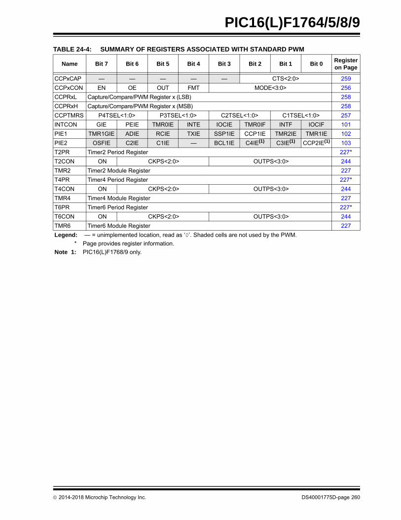
2014-2018 Microchip Technology Inc. DS40001775D-page 260
PIC16(L)F1764/5/8/9
TABLE 24-4: SUMMARY OF REGISTERS ASSOCIATED WITH STANDARD PWM
Name Bit 7 Bit 6 Bit 5 Bit 4 Bit 3 Bit 2 Bit 1 Bit 0Register on Page
CCPxCAP — — — — — CTS<2:0> 259
CCPxCON EN OE OUT FMT MODE<3:0> 256
CCPRxL Capture/Compare/PWM Register x (LSB) 258
CCPRxH Capture/Compare/PWM Register x (MSB) 258
CCPTMRS P4TSEL<1:0> P3TSEL<1:0> C2TSEL<1:0> C1TSEL<1:0> 257
INTCON GIE PEIE TMR0IE INTE IOCIE TMR0IF INTF IOCIF 101
PIE1 TMR1GIE ADIE RCIE TXIE SSP1IE CCP1IE TMR2IE TMR1IE 102
PIE2 OSFIE C2IE C1IE — BCL1IE C4IE(1) C3IE(1) CCP2IE(1) 103
T2PR Timer2 Period Register 227*
T2CON ON CKPS<2:0> OUTPS<3:0> 244
TMR2 Timer2 Module Register 227
T4PR Timer4 Period Register 227*
T4CON ON CKPS<2:0> OUTPS<3:0> 244
TMR4 Timer4 Module Register 227
T6PR Timer6 Period Register 227*
T6CON ON CKPS<2:0> OUTPS<3:0> 244
TMR6 Timer6 Module Register 227
Legend: — = unimplemented location, read as ‘0’. Shaded cells are not used by the PWM.
* Page provides register information.
Note 1: PIC16(L)F1768/9 only.

2014-2018 Microchip Technology Inc. DS40001775D-page 261
PIC16(L)F1764/5/8/9
25.0 10-BIT PULSE-WIDTH MODULATION (PWM) MODULE
The 10-bit PWM module generates a Pulse-WidthModulated signal determined by the duty cycle, periodand resolution that are configured by the followingregisters:
• T2PR• T2CON• PWMxDCH• PWMxDCL• PWMxCON
Figure 25-1 shows a simplified block diagram of PWMoperation.
Figure 25-2 shows a typical waveform of the PWMsignal.
FIGURE 25-1: SIMPLIFIED PWM BLOCK DIAGRAM
PWMxDCH
Comparator
TMR2
Comparator
T2PR
(1)
Duty Cycle Registers PWMxDCL<7:6>
Clear Timer,PWMx Pin and Latch Duty Cycle
PWMx
Note 1: The 8-bit timer is concatenated with the two Least Significant bits of 1/FOSC, adjusted by the Timer2 prescaler to create a 10-bit time base.
Latched(not visible to user)
Output Polarity (PWMxPOL)
TMR2 Module
0
1
PWMxOUT
To Other Peripherals: ADC, COG, CLC,
TRISx
PPS
RXYPPS
PRG, DSM, Op Amp Override
R Q
S Q

2014-2018 Microchip Technology Inc. DS40001775D-page 262
PIC16(L)F1764/5/8/9
For a step-by-step procedure on how to set up this mod-ule for PWM operation, refer to Section 25.10.1 “Setupfor PWM Operation Using PWMx Output Pins”.
FIGURE 25-2: PWM OUTPUT
25.1 PWMx Pin Configuration
All PWM outputs are multiplexed with the PORT datalatch. The user must configure the pins as outputs byclearing the associated TRISx bits.
25.2 Fundamental Operation
The PWM module produces a 10-bit resolution output.Timer2 and T2PR set the period of the PWM. ThePWMxDCL and PWMxDCH registers configure theduty cycle. The period is common to all PWM modules,whereas the duty cycle is independently controlled.
All PWM outputs associated with Timer2 are set whenTMR2 is cleared. Each PWMx is cleared when TMR2is equal to the value specified in the correspondingPWMxDCH (8 MSbs) and PWMxDCL<7:6> (2 LSbs)registers. When the value is greater than or equal toT2PR, the PWM output is never cleared (100% dutycycle).
25.3 PWM Output Polarity
The output polarity is inverted by setting the PWMxPOLbit of the PWMxCON register.
25.4 PWM Period
The PWM period is specified by the T2PR register ofTimer2. The PWM period can be calculated using theformula of Equation 25-1.
EQUATION 25-1: PWM PERIOD
When TMR2 is equal to T2PR, the following threeevents occur on the next increment cycle:
• TMR2 is cleared
• The PWM output is active. (Exception: When the PWM duty cycle = 0%, the PWM output will remain inactive.)
• The PWMxDCH and PWMxDCL register values are latched into the buffers.
25.5 PWM Duty Cycle
The PWM duty cycle is specified by writing a 10-bit valueto the PWMxDCH and PWMxDCL register pair. ThePWMxDCH register contains the eight MSbs and thePWMxDCL<7:6>, the two LSbs. The PWMxDCH andPWMxDCL registers can be written to at any time.
Equation 25-2 is used to calculate the PWM pulsewidth.
Equation 25-3 is used to calculate the PWM duty cycleratio.
EQUATION 25-2: PULSE WIDTH
EQUATION 25-3: DUTY CYCLE RATIO
The 8-bit timer TMR2 register is concatenated with thetwo Least Significant bits of 1/FOSC, adjusted by theTimer2 prescaler to create the 10-bit time base. Thesystem clock is used if the Timer2 prescaler is set to 1:1.
25.6 PWM Resolution
The resolution determines the number of available dutycycles for a given period. For example, a 10-bit resolutionwill result in 1024 discrete duty cycles, whereas an 8-bitresolution will result in 256 discrete duty cycles.
Note: The Timer2 postscaler is not used in thedetermination of the PWM frequency. Thepostscaler could be used to have a servoupdate rate at a different frequency than thePWM output.
Note: The PWMxDCH and PWMxDCL registersare double-buffered. The buffers areupdated when Timer2 matches T2PR. Careshould be taken to update both registersbefore the timer match occurs.
Period
Pulse Width
TMR2 = 0
TMR2 =
TMR2 = T2PR
PWMxDCH<7:0>:PWMxDCL<7:6>
Note: The Timer2 postscaler has no effect on thePWM operation.
PWM Period T2PR 1+ 4 TOSC =
(TMR2 Prescale Value)
Note: TOSC = 1/FOSC.
Pulse Width PWMxDCH:PWMxDCL<7:6> =
TOSC (TMR2 Prescale Value)
Note: TOSC = 1/FOSC.
Duty Cycle RatioPWMxDCH:PWMxDCL<7:6>
4 T2PR 1+ -----------------------------------------------------------------------------------=

2014-2018 Microchip Technology Inc. DS40001775D-page 263
PIC16(L)F1764/5/8/9
The maximum PWM resolution is ten bits when T2PRis 255. The resolution is a function of the T2PR registervalue as shown by Equation 25-4.
EQUATION 25-4: PWM RESOLUTION
25.7 Operation in Sleep Mode
In Sleep mode, the TMR2 register will not incrementand the state of the module will not change. If thePWMx pin is driving a value, it will continue to drive thatvalue. When the device wakes up, TMR2 will continuefrom its previous state.
25.8 Changes in System Clock Frequency
The PWM frequency is derived from the system clockfrequency (FOSC). Any changes in the system clockfrequency will result in changes to the PWM frequency.Refer to Section 5.0 “Oscillator Module (withFail-Safe Clock Monitor)” for additional details.
25.9 Effects of Reset
Any Reset will force all ports to Input mode and thePWM registers to their Reset states.
Resolution4 T2PR 1+ log
2 log---------------------------------------------- bits=
Note: If the pulse-width value is greater than theperiod the assigned PWM pin(s) willremain unchanged.
TABLE 25-1: EXAMPLE PWM FREQUENCIES AND RESOLUTIONS (FOSC = 20 MHz)
PWM Frequency 0.31 kHz 4.88 kHz 19.53 kHz 78.12 kHz 156.3 kHz 208.3 kHz
Timer Prescale 64 4 1 1 1 1
T2PR Value 0xFF 0xFF 0xFF 0x3F 0x1F 0x17
Maximum Resolution (bits) 10 10 10 8 7 6.6
TABLE 25-2: EXAMPLE PWM FREQUENCIES AND RESOLUTIONS (FOSC = 8 MHz)
PWM Frequency 0.31 kHz 4.90 kHz 19.61 kHz 76.92 kHz 153.85 kHz 200.0 kHz
Timer Prescale 64 4 1 1 1 1
T2PR Value 0x65 0x65 0x65 0x19 0x0C 0x09
Maximum Resolution (bits) 8 8 8 6 5 5

2014-2018 Microchip Technology Inc. DS40001775D-page 264
PIC16(L)F1764/5/8/9
25.10 Set-up Procedures
25.10.1 SETUP FOR PWM OPERATION USING PWMx OUTPUT PINS
The following steps should be taken when configuringthe module for PWM operation using the PWMx outputpins:
1. Disable the PWMx pin output driver(s) by settingthe associated TRISx bit(s).
2. Clear the PWMxCON register.
3. Load the T2PR register with the PWM periodvalue.
4. Load the PWMxDCH register and bits<7:6> ofthe PWMxDCL register with the PWM duty cyclevalue.
5. Configure and start Timer2:
• Clear the TMR2IF interrupt flag bit of the PIR1 register. See Note below.
• Configure the CKPSx bits of the T2CON register with the Timer2 prescale value.
• Enable Timer2 by setting the ON bit of the T2CON register.
6. Enable the PWM output pin and wait untilTimer2 overflows. TMR2IF bit of the PIR1register is set. See Note below.
7. Enable the PWMx pin output driver(s) by clear-ing the associated TRISx bit(s) and setting thedesired pin PPS control bits.
8. Configure the PWM module by loading thePWMxCON register with the appropriate values.
25.10.2 SETUP FOR PWM OPERATION TO OTHER DEVICE PERIPHERALS
The following steps should be taken when configuringthe module for PWM operation to be used by otherdevice peripherals:
1. Disable the PWMx pin output driver(s) by settingthe associated TRISx bit(s).
2. Clear the PWMxCON register.
3. Load the T2PR register with the PWM periodvalue.
4. Load the PWMxDCH register and bits<7:6> ofthe PWMxDCL register with the PWM duty cyclevalue.
5. Configure and start Timer2:
• Clear the TMR2IF interrupt flag bit of the PIR1 register. See Note below.
• Configure the CKPSx bits of the T2CON register with the Timer2 prescale value.
• Enable Timer2 by setting the ON bit of the T2CON register.
6. Enable PWM output pin:
• Wait until Timer2 overflows, TMR2IF bit of the PIR1 register is set. See Note below.
7. Configure the PWM module by loading thePWMxCON register with the appropriate values.
Note 1: In order to send a complete duty cycleand period on the first PWM output, theabove steps must be followed in the ordergiven. If it is not critical to start with acomplete PWM signal, then move Step 8to replace Step 4.
2: For operation with other peripherals only,disable PWMx pin outputs.
Note: In order to send a complete duty cycle andperiod on the first PWM output, the abovesteps must be included in the setupsequence. If it is not critical to start with acomplete PWM signal on the first output,then Step 6 may be ignored.

2014-2018 Microchip Technology Inc. DS40001775D-page 265
PIC16(L)F1764/5/8/9
25.11 Register Definitions: 10-Bit PWM Control
Long bit name prefixes for the PWM peripherals areshown in Table 25-3. Refer to Section 1.1.2.2 “LongBit Names” for more information.
TABLE 25-3: BIT NAME PREFIXES
Peripheral Bit Name Prefix
PWM3 PWM3
PWM4(1) PWM4
Note 1: PIC16(L)F1768/9 devices only.
REGISTER 25-1: PWMxCON: PWMx CONTROL REGISTER
R/W-0/0 U-0 R-0/0 R/W-0/0 U-0 U-0 U-0 U-0
EN — OUT POL — — — —
bit 7 bit 0
Legend:
R = Readable bit W = Writable bit
u = Bit is unchanged x = Bit is unknown U = Unimplemented bit, read as ‘0’
‘1’ = Bit is set ‘0’ = Bit is cleared -n/n = Value at POR and BOR/Value at all other Resets
bit 7 EN: PWMx Module Enable bit
1 = PWMx module is enabled0 = PWMx module is disabled
bit 6 Unimplemented: Read as ‘0’
bit 5 OUT: PWMx Module Output Level When Read bit
bit 4 POL: PWMx Output Polarity Select bit
1 = PWMx output is active-low0 = PWMx output is active-high
bit 3-0 Unimplemented: Read as ‘0’

2014-2018 Microchip Technology Inc. DS40001775D-page 266
PIC16(L)F1764/5/8/9
REGISTER 25-2: PWMxDCH: PWMx DUTY CYCLE REGISTER HIGH BITS
R/W-x/u R/W-x/u R/W-x/u R/W-x/u R/W-x/u R/W-x/u R/W-x/u R/W-x/u
DC<9:2>
bit 7 bit 0
Legend:
R = Readable bit W = Writable bit
u = Bit is unchanged x = Bit is unknown U = Unimplemented bit, read as ‘0’
‘1’ = Bit is set ‘0’ = Bit is cleared -n/n = Value at POR and BOR/Value at all other Resets
bit 7-0 DC<9:2>: PWM Duty Cycle Most Significant bits
These bits are the MSbs of the PWM duty cycle. The two LSbs are found in the PWMxDCL register.
REGISTER 25-3: PWMxDCL: PWMx DUTY CYCLE REGISTER LOW BITS
R/W-x/u R/W-x/u U-0 U-0 U-0 U-0 U-0 U-0
DC<1:0> — — — — — —
bit 7 bit 0
Legend:
R = Readable bit W = Writable bit
u = Bit is unchanged x = Bit is unknown U = Unimplemented bit, read as ‘0’
‘1’ = Bit is set ‘0’ = Bit is cleared -n/n = Value at POR and BOR/Value at all other Resets
bit 7-6 DC<1:0>: PWM Duty Cycle Least Significant bits
These bits are the LSbs of the PWM duty cycle. The MSbs are found in the PWMxDCH register.
bit 5-0 Unimplemented: Read as ‘0’
TABLE 25-4: SUMMARY OF REGISTERS ASSOCIATED WITH 10-BIT PWM
Name Bit 7 Bit 6 Bit 5 Bit 4 Bit 3 Bit 2 Bit 1 Bit 0Register on Page
CCPTMRS P4TSEL<1:0> P3TSEL<1:0> C2TSEL<1:0>(1) C1TSEL<1:0> 264
PWMxCON EN — OUT POL MODE<1:0> — — 265
PWMxDCH DC<9:2> 266
PWMxDCL DC<1:0> — — — — — — 266
RxyPPS — — — RxyPPS<4:0> 154
TxCON ON CKPS<2:0> OUTPS<3:0> 244
TxCLKCON — — — — CS<3:0> 243
TxPR TMRx Period Register 227
TRISA — — TRISA<5:4> —(1) TRISA<2:0> 136
TRISB(2) TRISB<7:4> — — — — 142
TRISC TRISC7(2) TRISC6(2) TRISC5 TRISC4 TRISC3 TRISC2 TRISC1 TRISC0 147
Legend: — = Unimplemented location, read as ‘0’. Shaded cells are not used by the PWM.Note 1: Unimplemented, read as ‘1’.
2: PIC16(L)F1768/9 only.

2014-2018 Microchip Technology Inc. DS40001775D-page 267
PIC16(L)F1764/5/8/9
26.0 16-BIT PULSE-WIDTH MODULATION (PWM) MODULE
The Pulse-Width Modulation (PWM) module generatesa Pulse-Width Modulated signal determined by thephase, duty cycle, period and offset event counts thatare contained in the following registers:
• PWMxPH registers• PWMxDC registers• PWMxPR registers• PWMxOF registers
Figure 26-1 shows a simplified block diagram of thePWM operation.
Each PWM module has four modes of operation:
• Standard• Set On Match• Toggle On Match• Center-Aligned
For a more detailed description of each PWM mode,refer to Section 26.2 “PWM Modes”.
Each PWM module has four Offset modes:
• Independent Run
• Slave Run with Synchronous Start
• One-Shot Slave with Synchronous Start
• Continuous Run Slave with Synchronous Start and Timer Reset
Using the Offset modes, each PWM module can offsetits waveform relative to any other PWM module in thesame device. For a more detailed description of theOffset modes, refer to Section 26.3 “Offset Modes”.
Every PWM module has a configurable reloadoperation to ensure all event count buffers change atthe end of a period, thereby avoiding signal glitches.Figure 26-2 shows a simplified block diagram of thereload operation. For a more detailed description ofthe reload operation, refer to Section 26.4 “ReloadOperation”.
FIGURE 26-1: 16-BIT PWMx BLOCK DIAGRAM
Rev. 10-000 152B4/22/201 4
PWM ControlUnit
MODE<1:0>
PWMxPR
Comparator
PWMxTMR
PRx_match
PWMxDC
Comparator
16-bt Latch
DCx_match
PWMxOF
Comparator
16-bt Latch
OFx_match
PWMxPH
Comparator
16-bt Latch
PHx_match
16-bt Latch LDx_trigger LDx_trigger LDx_trigger LDx_trigger
PWMxPOL
PWMx
PWMxOUT
To Peripherals
TRIS Control
set PRIF set PHIF set OFIF set DCIF
D
CK
Q
Q4
PWMx_output
OffsetControl
E R U/D
OFM<1:0>
PRx_match
OF6_match(1)
OF5_match(1)
OFS
OF_match
ENPHx_match
DCx_match
Note 1: A PWM module cannot trigger from its own offset match event. The input corresponding to a PWM module’s own offset match is reserved.
PWM_clock
PPS
RxyPPS
10

2014-2018 Microchip Technology Inc. DS40001775D-page 268
PIC16(L)F1764/5/8/9
FIGURE 26-2: LOAD TRIGGER BLOCK DIAGRAM
26.1 Fundamental Operation
The PWM module produces a 16-bit resolutionPulse-Width Modulated output.
Each PWM module has an independent timer driven bya selection of clock sources determined by thePWMxCLKCON register (Register 26-4). The timervalue is compared to Event Count registers to generatethe various events of a the PWM waveform, such as theperiod and duty cycle. For a block diagram describingthe clock sources, refer to Figure 26-3.
Each PWM module can be enabled individually usingthe EN bit of the PWMxCON register, or several PWMmodules can be enabled simultaneously using theMPWMxEN bits of the PWMEN register.
The current state of the PWM output can be read usingthe OUT bit of the PWMxCON register. In some modes,this bit can be set and cleared by software, givingadditional software control over the PWM waveform.This bit is synchronized to FOSC/4 and therefore, doesnot change in real time with respect to the PWM_clock.
FIGURE 26-3: PWMx CLOCK SOURCE BLOCK DIAGRAM
26.1.1 PWMx PIN CONFIGURATION
This device uses the PPS control circuitry to routeperipherals to any device I/O pin. Select the desiredpin, or pins, for PWM output with the device pin, usingthe RxyPPS control register (Register 12-2).
All PWM outputs are multiplexed with the PORT datalatch, so the pins must also be configured as outputs byclearing the associated PORT TRISx bits.
The slew rate feature may be configured to optimizethe rate to be used in conjunction with the PWM _out-puts. High-speed output switching is attained byclearing the associated PORT SLRCONx bits.
The PWM outputs can be configured to be open-drainoutputs by setting the associated PORT ODCONx bits.
26.1.2 PWMx Output Polarity
The output polarity is inverted by setting the POL bit ofthe PWMxCON register. The polarity control affects thePWM output even when the module is not enabled.
Rev. 10-000 153B7/9/201 5
LDx_trigger(1)
LDy_trigger
PWMxLDS
PRx_match
10
PWMxLDA(2)D Q
PWM_clock
LDx_trigger
PWMxLDT
Note 1. The input corresponding to a PWM module’s own load trigger is reserved.2. PWMxLDA is cleared by hardware upon LDx_trigger.
Note: If PWM_clock > FOSC/4, the OUT bit maynot accurately represent the output state ofthe PWM.
Rev. 10-000156A1/7/2015
00
11
10
01HFINTOSC
LFINTOSC
FOSC
Reserved
PWMxCS<1:0>
Prescaler PWMx_clock
PWMxPS<2:0>

2014-2018 Microchip Technology Inc. DS40001775D-page 269
PIC16(L)F1764/5/8/9
26.2 PWM Modes
PWM modes are selected with the MODE<1:0> bits ofthe PWMxCON register (Register 26-1).
In all PWM modes, an offset match event can also beused to synchronize the PWMxTMR in three Offsetmodes. See Section 26.3 “Offset Modes” for moreinformation.
26.2.1 STANDARD MODE
The Standard mode (MODE<1:0> = 00) selects asingle-phase PWM output. The PWM output in this modeis determined by when the period, duty cycle and phasecounts match the PWMxTMR value. The start of the dutycycle occurs on the phase match and the end of the dutycycle occurs on the duty cycle match. The period matchresets the timer. The offset match can also be used tosynchronize the PWMxTMR in the Offset modes. SeeSection 26.3 “Offset Modes” for more information.
Equation 26-1 is used to calculate the PWM period inStandard mode.
Equation 26-2 is used to calculate the PWM duty cycleratio in Standard mode.
EQUATION 26-1: PWM PERIOD IN STANDARD MODE
EQUATION 26-2: PWM DUTY CYCLE IN STANDARD MODE
A detailed timing diagram for Standard mode is shownin Figure 26-4.
26.2.2 SET ON MATCH MODE
The Set On Match mode (MODE<1:0> = 01) generatesan active output when the phase count matches thePWMxTMR value. The output stays active until theOUT bit of the PWMxCON register is cleared or thePWM module is disabled. The duty cycle count has noeffect in this mode. The period count only determinesthe maximum PWMxTMR value above which no phasematches can occur.
The PWMxOUT bit can be used to set or clear the out-put of the PWM in this mode. Writes to this bit will takeplace on the next rising edge of the PWM_clock afterthe bit is written.
A detailed timing diagram for Set On Match mode isshown in Figure 26-5.
26.2.3 TOGGLE ON MATCH MODE
The Toggle On Match mode (MODE<1:0> = 10) gener-ates a 50% duty cycle PWM with a period twice as longas that computed for the Standard PWM mode. Dutycycle count has no effect in this mode. The phase countdetermines how many PWMxTMR periods, after aperiod event, the output will toggle.
Writes to the OUT bit of the PWMxCON register willhave no effect in this mode.
A detailed timing diagram for Toggle On Match mode isshown in Figure 26-6.
26.2.4 CENTER-ALIGNED MODE
The Center-Aligned mode (MODE<1:0> = 11)generates a PWM waveform that is centered in theperiod. In this mode, the period is two times thePWMxPR count. The PWMxTMR counts up to theperiod value, then counts back down to 0. The dutycycle count determines both the start and end of theactive PWM output. The start of the duty cycle occursat the match event when PWMxTMR is incrementing,and the duty cycle ends at the match event whenPWMxTMR is decrementing. The incrementing matchvalue is the period count minus the duty cycle count.The decrementing match value is the incrementingmatch value plus 1.
Equation 26-3 is used to calculate the PWM period inCenter-Aligned mode.
EQUATION 26-3: PWM PERIOD IN CENTER-ALIGNED MODE
Equation 26-4 is used to calculate the PWM duty cycleratio in Center-Aligned mode
EQUATION 26-4: PWM DUTY CYCLE IN CENTER-ALIGNED MODE
Writes to PWMxOUT will have no effect in this mode.
A detailed timing diagram for Center-Aligned mode isshown in Figure 26-7.
PeriodPWMxPR 1+ Prescale
PWM_clock----------------------------------------------------------------------=
Duty CyclePWMxDC PWMxPH–
PWMxPR 1+-----------------------------------------------------------------=
PeriodPWMxPR 1+ 2 Prescale
PWM_clock------------------------------------------------------------------------------=
Duty CyclePWMxDC 2
PWMxPR 1+ 2-------------------------------------------------=
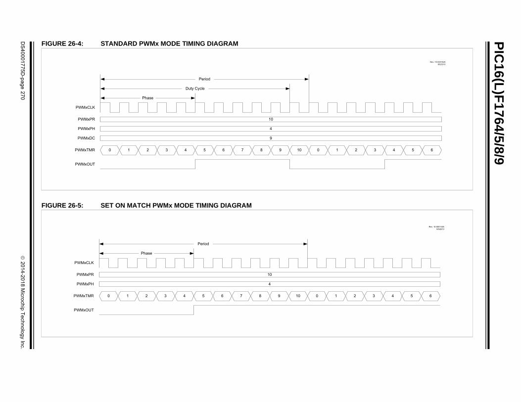
PIC
16(L
)F1
764
/5/8
/9
DS
40
00
17
75
D-p
ag
e 2
70
2
01
4-2
01
8 M
icroch
ip T
ech
no
log
y Inc.
FIGURE 26-4: STANDARD PWMx MODE TIMING DIAGRAM
FIGURE 26-5: SET ON MATCH PWMx MODE TIMING DIAGRAM
Rev. 10-000142A9/5/2013
PWMxCLK
10
4
9
PWMxPR
PWMxPH
PWMxDC
Phase
Duty Cycle
Period
0 1 2 3 4 5 6 7 8 9 10 0 1 2 3 4 5 6PWMxTMR
PWMxOUT
Rev. 10-000143A9/5/2013
PWMxCLK
10
4
PWMxPR
PWMxPH
Phase
Period
0 1 2 3 4 5 6 7 8 9 10 0 1 2 3 4 5 6PWMxTMR
PWMxOUT

2
01
4-2
01
8 M
icroch
ip T
ech
no
log
y Inc.
DS
40
00
17
75
D-p
ag
e 2
71
PIC
16(L
)F17
64/5/8/9
FIGURE 26-6: TOGGLE ON MATCH PWMx MODE TIMING DIAGRAM
FIGURE 26-7: CENTER-ALIGNED PWMx MODE TIMING DIAGRAM
Rev. 10-000144A9/5/2013
PWMxCLK
10
4
PWMxPR
PWMxPH
Phase
Period
0 1 2 3 4 5 6 7 8 9 10 0 1 2 3 4 5 6PWMxTMR
PWMxOUT
Rev. 10-000 145A4/22/201 4
PWMxCLK
6
4
PWMxPR
PWMxDC
Duty Cycle
Period
0 1 2 3 4 5 6 6 5 4 3 2 1 0 0 1 2 3PWMxTMR
PWMxOUT

2014-2018 Microchip Technology Inc. DS40001775D-page 272
PIC16(L)F1764/5/8/9
26.3 Offset Modes
The Offset modes provide the means to adjust the wave-form of a slave PWM module relative to the waveform ofa master PWM module in the same device.
26.3.1 INDEPENDENT RUN MODE
In Independent Run mode (OFM<1:0> = 00), the PWMmodule is unaffected by the other PWM modules in thedevice. The PWMxTMR associated with the PWMmodule in this mode starts counting as soon as the EN bitassociated with this PWM module is set, and continuescounting until the EN bit is cleared. Period events resetthe PWMxTMR to zero, after which, the timer continuesto count.
A detailed timing diagram of this mode used withStandard PWM mode is shown in Figure 26-8.
26.3.2 SLAVE RUN MODE WITH SYNC START
In Slave Run mode with Sync Start (OFM<1:0> = 01),the slave PWMxTMR waits for the master’s OF_matchevent. When this event occurs, if the EN bit is set, thePWMxTMR begins counting and continues to countuntil software clears the EN bit. Slave period eventsreset the PWMxTMR to zero, after which, the timercontinues to count.
A detailed timing diagram of this mode used withStandard PWM mode is shown in Figure 26-9.
26.3.3 ONE-SHOT SLAVE MODE WITH SYNC START
In One-Shot Slave mode with Synchronous Start(OFM<1:0> = 10), the slave PWMxTMR waits until themaster’s OF_match event. The timer then begins count-ing, starting from the value that is already in the timer, andcontinues to count until the period match event. When theperiod event occurs, the timer resets to zero and stopscounting. The timer then waits until the next masterOF_match event, after which, it begins counting again torepeat the cycle. An OF_match event that occurs beforethe slave PWM has completed the triggered period will beignored. A slave period that is greater than the masterperiod, but less that twice the master period, will result ina slave output every other master period.
A detailed timing diagram of this mode used withStandard PWM mode is shown in Figure 26-10.
26.3.4 CONTINUOUS RUN SLAVE MODE WITH SYNC START AND TIMER RESET
In Continuous Run Slave mode with Synchronous Startand Timer Reset (OFM<1:0> = 11), the slave PWMxTMRis inhibited from counting after the slave PWM enable isset. The first master OF_match event starts the slavePWMxTMR. Subsequent master OF_match events resetthe slave PWMxTMR timer value back to 1, after which,the slave PWMxTMR continues to count. The next masterOF_match event resets the slave PWMxTMR back to 1 torepeat the cycle. Slave period events that occur beforethe master’s OF_match event will reset the slavePWMxTMR to zero, after which, the timer will continue tocount. Slaves operating in this mode must have aPWMxPH register pair value equal to, or greater than, 1;otherwise, the phase match event will not occurprecluding the start of the PWM output duty cycle.
The offset timing will persist if both the master andslave PWMxPR values are the same and the SlaveOffset mode is changed to Independent Run modewhile the PWM module is operating.
A detailed timing diagram of this mode used inStandard PWM mode is shown in Figure 26-11.
26.3.5 OFFSET MATCH IN CENTER-ALIGNED MODE
When a master is operating in Center-Aligned mode,the offset match event depends on which direction thePWMxTMR is counting. Clearing the OFO bit of thePWMxOFCON register will cause the OF_match eventto occur when the timer is counting up. Setting the OFObit of the PWMxOFCON register will cause theOF_match event to occur when the timer is countingdown. The OFO bit is ignored in Non-Center-Alignedmodes.
The OFO bit is double-buffered and requires setting theLDA bit to take effect when the PWM module isoperating.
Detailed timing diagrams of Center-Aligned modeusing offset match control in Independent Slave withSync Start mode can be seen in Figure 26-12 andFigure 26-13.
Note: During the time the slave timers areresetting to zero, if another offset matchevent is received, it is possible that the slavePWM would not recognize this match eventand the slave timers would fail to begincounting again. This would result in missingduty cycles in the output of the slave PWM.To prevent this from happening, avoid usingthe same period for both the master andslave PWMs.
Note: Unexpected results will occur if the slavePWM_clock is a higher frequency than themaster PWM_clock.

2
01
4-2
01
8 M
icroch
ip T
ech
no
log
y Inc.
DS
40
00
17
75
D-p
ag
e 2
73
PIC
16(L
)F17
64/5/8/9
FIGURE 26-8: INDEPENDENT RUN MODE TIMING DIAGRAM
Rev. 10-000 146B7/8/201 5
PWMxCLK
10
3
5
2
PWMxPR
PWMxPH
PWMxDC
PWMxOF
Offset
Phase
Duty Cycle
Period
0 1 2 3 4 5 6 7 8 9 10 0 1 2 3 4 5 6PWMxTMR
PWMxOUT
OFx_match
PHx_match
DCx_match
PRx_match
0 1 2 3 4 0 1 2 3 4 0 1 2 3 4 0 1 2PWMyTMR
4
0
1
PWMyPR
PWMyPH
PWMyDC
PWMyOUT
Note: PWMx = Master, PWMy = Slave

PIC
16(L
)F1
764
/5/8
/9
DS
40
00
17
75
D-p
ag
e 2
74
2
01
4-2
01
8 M
icroch
ip T
ech
no
log
y Inc.
FIGURE 26-9: SLAVE RUN MODE WITH SYNC START TIMING DIAGRAM
Rev. 10-000 147B7/8/201 5
PWMxCLK
10
3
5
2
PWMxPR
PWMxPH
PWMxDC
PWMxOF
Offset
Phase
Duty Cycle
Period
0 1 2 3 4 5 6 7 8 9 10 0 1 2 3 4 5 6PWMxTMR
PWMxOUT
OFx_match
PWMyTMR
4
0
1
PWMyPR
PWMyPH
PWMyDC
PWMyOUT
10 2 3 4 0 1 2 3 4 0 1 2 3 4 0
Note: Master = PWMx, Slave = PWMy
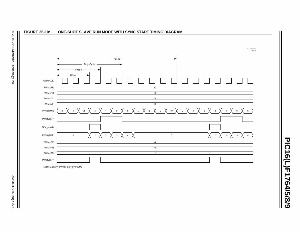
2
01
4-2
01
8 M
icroch
ip T
ech
no
log
y Inc.
DS
40
00
17
75
D-p
ag
e 2
75
PIC
16(L
)F17
64/5/8/9
FIGURE 26-10: ONE-SHOT SLAVE RUN MODE WITH SYNC START TIMING DIAGRAM
Rev. 10-000 148B7/8/201 5
PWMxCLK
10
3
5
2
PWMxPR
PWMxPH
PWMxDC
PWMxOF
Offset
Phase
Duty Cycle
Period
0 1 2 3 4 5 6 7 8 9 10 0 1 2 3 4 5 6PWMxTMR
PWMxOUT
OFx_match
PWMyTMR
4
0
1
PWMyPR
PWMyPH
PWMyDC
PWMyOUT
10 2 3 4 1 2 3 40
Note: Master = PWMx, Slave = PWMy

PIC
16(L
)F1
764
/5/8
/9
DS
40
00
17
75
D-p
ag
e 2
76
2
01
4-2
01
8 M
icroch
ip T
ech
no
log
y Inc.
FIGURE 26-11: CONTINUOUS SLAVE RUN MODE WITH IMMEDIATE RESET AND SYNC START TIMING DIAGRAM
Rev. 10-000 149B7/8/201 5
PWMxCLK
10
3
5
2
PWMxPR
PWMxPH
PWMxDC
PWMxOF
Offset
Phase
Duty Cycle
Period
0 1 2 3 4 5 6 7 8 9 10 0 1 2 3 4 5 6PWMxTMR
PWMxOUT
OFx_match
PWMyTMR
4
1
2
PWMyPR
PWMyPH
PWMyDC
PWMyOUT
10 2 3 4 1 2 3 401 2 3 40 1
Note: Master= PWMx, Slave=PWMy

2
01
4-2
01
8 M
icroch
ip T
ech
no
log
y Inc.
DS
40
00
17
75
D-p
ag
e 2
77
PIC
16(L
)F17
64/5/8/9
FIGURE 26-12: OFFSET MATCH ON INCREMENTING TIMER TIMING DIAGRAM
Rev. 10-000 150B7/9/201 5
PWMxCLK
6
2
2
PWMxPR
PWMxDC
PWMxOF
Offset
Duty Cycle
Period
0 1 2 3 4 5 6 6 5 4 3 2 1 0 0 1 2 3PWMxTMR
PWMxOUT
OFx_match
PHx_match
DCx_match
PRx_match
0 12 3 4 4 3 2 1 0PWMyTMR
4
1
PWMyPR
PWMyDC
PWMyOUT
0100
Note: Master = PWMx, Slave = PWMy

PIC
16(L
)F1
764
/5/8
/9
DS
40
00
17
75
D-p
ag
e 2
78
2
01
4-2
01
8 M
icroch
ip T
ech
no
log
y Inc.
FIGURE 26-13: OFFSET MATCH ON DECREMENTING TIMER TIMING DIAGRAM
Rev. 10-000 151B7/9/201 5
PWMxCLK
6
2
2
PWMxPR
PWMxDC
PWMxOF
Offset
Duty Cycle
Period
0 1 2 3 4 5 6 6 5 4 3 2 1 0 0 1 2 3PWMxTMR
PWMxOUT
OF5_match
PH5_match
DC5_match
PR5_match
PWMyTMR
4
1
PWMyPR
PWMyDC
PWMyOUT
0 1 2 3 4 4 30
Note: Master = PWMx, Slave = PWMy
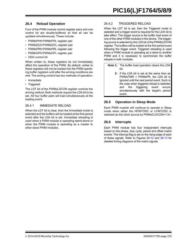
2014-2018 Microchip Technology Inc. DS40001775D-page 279
PIC16(L)F1764/5/8/9
26.4 Reload Operation
Four of the PWM module control register pairs and onecontrol bit are double-buffered so that all can beupdated simultaneously. These include:
• PWMxPHH:PWMxPHL register pair
• PWMxDCH:PWMxDCL register pair
• PWMxPRH:PWMxPRL register pair
• PWMxOFH:PWMxOFL register pair
• ODO control bit
When written to, these registers do not immediatelyaffect the operation of the PWM. By default, writes tothese registers will not be loaded into the PWM operat-ing buffer registers until after the arming conditions aremet. The arming control has two methods of operation:
• Immediate
• Triggered
The LDT bit of the PWMxLDCON register controls thearming method. Both methods require the LDA bit to beset. All four buffer pairs will load simultaneously at theloading event.
26.4.1 IMMEDIATE RELOAD
When the LDT bit is clear, then the Immediate mode isselected and the buffers will be loaded at the first periodevent after the LDA bit is set. Immediate reloading isused when a PWM module is operating stand-alone orwhen the PWM module is operating as a master toother slave PWM modules.
26.4.2 TRIGGERED RELOAD
When the LDT bit is set, then the Triggered mode isselected and a trigger event is required for the LDA bit totake effect. The trigger source is the buffer load event ofone of the other PWM modules in the device. The trigger-ing source is selected by the LDS bit of the PWMxLDCONregister. The buffers will be loaded at the first period eventfollowing the trigger event. Triggered reloading is usedwhen a PWM module is operating as a slave to anotherPWM and it is necessary to synchronize the bufferreloads in both modules.
26.5 Operation in Sleep Mode
Each PWM module will continue to operate in Sleepmode when either the HFINTOSC or LFINTOSC isselected as the clock source by PWMxCLKCON<1:0>.
26.6 Interrupts
Each PWM module has four independent interruptsbased on the phase, duty cycle, period and offset matchevents. The interrupt flag is set on the rising edge of eachof these signals. Refer to Figures 26-12 and 26-13 fordetailed timing diagrams of the match signals.
Note 1: The buffer load operation clears the LDAbit.
2: If the LDA bit is set at the same time asPWMxTMR = PWMxPR, the LDA bit isignored until the next period event. Such isthe case when triggered reload is selectedand the triggering event occurssimultaneously with the target’s periodevent.

2014-2018 Microchip Technology Inc. DS40001775D-page 280
PIC16(L)F1764/5/8/9
26.7 Register Definitions: PWM Control
Long bit name prefixes for the 16-bit PWM peripheralsare shown in Table 26-1. Refer to Section 1.1 “Registerand Bit Naming Conventions” for more information.
TABLE 26-1: BIT NAME PREFIXES
Peripheral Bit Name Prefix
PWM5 PWM5
PWM6(1) PWM6
Note 1: PIC16(L)F1768/9 devices only.
REGISTER 26-1: PWMxCON: PWMx CONTROL REGISTER
R/W-0/0 U-0 R/HS/HC-0/0 R/W-0/0 R/W-0/0 R/W-0/0 U-0 U-0
EN — OUT POL MODE<1:0> — —
bit 7 bit 0
Legend:
R = Readable bit W = Writable bit
HC = Hardware Clearable bit HS = Hardware Settable bit U = Unimplemented bit, read as ‘0’
‘1’ = Bit is set ‘0’ = Bit is cleared -n/n = Value at POR and BOR/Value at all other Resets
bit 7 EN: PWMx Module Enable bit
1 = Module is enabled0 = Module is disabled
bit 6 Unimplemented: Read as ‘0’
bit 5 OUT: Output State of the PWMx Module bit
bit 4 POL: PWMx Output Polarity Control bit
1 = PWMx output active state is low0 = PWMx output active state is high
bit 3-2 MODE<1:0>: PWMx Mode Control bits
11 = Center-Aligned mode10 = Toggle On Match mode01 = Set On Match mode00 = Standard PWM mode
bit 1-0 Unimplemented: Read as ‘0’
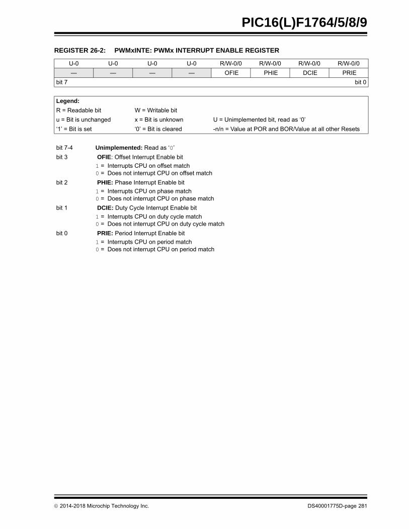
2014-2018 Microchip Technology Inc. DS40001775D-page 281
PIC16(L)F1764/5/8/9
REGISTER 26-2: PWMxINTE: PWMx INTERRUPT ENABLE REGISTER
U-0 U-0 U-0 U-0 R/W-0/0 R/W-0/0 R/W-0/0 R/W-0/0
— — — — OFIE PHIE DCIE PRIE
bit 7 bit 0
Legend:
R = Readable bit W = Writable bit
u = Bit is unchanged x = Bit is unknown U = Unimplemented bit, read as ‘0’
‘1’ = Bit is set ‘0’ = Bit is cleared -n/n = Value at POR and BOR/Value at all other Resets
bit 7-4 Unimplemented: Read as ‘0’
bit 3 OFIE: Offset Interrupt Enable bit
1 = Interrupts CPU on offset match0 = Does not interrupt CPU on offset match
bit 2 PHIE: Phase Interrupt Enable bit
1 = Interrupts CPU on phase match0 = Does not interrupt CPU on phase match
bit 1 DCIE: Duty Cycle Interrupt Enable bit
1 = Interrupts CPU on duty cycle match0 = Does not interrupt CPU on duty cycle match
bit 0 PRIE: Period Interrupt Enable bit
1 = Interrupts CPU on period match0 = Does not interrupt CPU on period match

2014-2018 Microchip Technology Inc. DS40001775D-page 282
PIC16(L)F1764/5/8/9
REGISTER 26-3: PWMxINTF: PWMx INTERRUPT REQUEST REGISTER
U-0 U-0 U-0 U-0 R/W/HS-0/0 R/W/HS-0/0 R/W/HS-0/0 R/W/HS-0/0
— — — — OFIF(1) PHIF(1) DCIF(1) PRIF(1)
bit 7 bit 0
Legend:
R = Readable bit W = Writable bit HS = Hardware Settable bit
u = Bit is unchanged x = Bit is unknown U = Unimplemented bit, read as ‘0’
‘1’ = Bit is set ‘0’ = Bit is cleared -n/n = Value at POR and BOR/Value at all other Resets
bit 7-4 Unimplemented: Read as ‘0’
bit 3 OFIF: Offset Interrupt Flag bit(1)
1 = Offset match event occurred0 = Offset match event did not occur
bit 2 PHIF: Phase Interrupt Flag bit(1)
1 = Phase match event occurred0 = Phase match event did not occur
bit 1 DCIF: Duty Cycle Interrupt Flag bit(1)
1 = Duty cycle match event occurred0 = Duty cycle match event did not occur
bit 0 PRIF: Period Interrupt Flag bit(1)
1 = Period match event occurred0 = Period match event did not occur
Note 1: Bit is forced clear by hardware while module is disabled (EN = 0).

2014-2018 Microchip Technology Inc. DS40001775D-page 283
PIC16(L)F1764/5/8/9
REGISTER 26-4: PWMxCLKCON: PWMx CLOCK CONTROL REGISTER
U-0 R/W-0/0 R/W-0/0 R/W-0/0 U-0 U-0 R/W-0/0 R/W-0/0
— PS<2:0> — — CS<1:0>
bit 7 bit 0
Legend:
R = Readable bit W = Writable bit
u = Bit is unchanged x = Bit is unknown U = Unimplemented bit, read as ‘0’
‘1’ = Bit is set ‘0’ = Bit is cleared -n/n = Value at POR and BOR/Value at all other Resets
bit 7 Unimplemented: Read as ‘0’
bit 6-4 PS<2:0>: Clock Source Prescaler Select bits
111 = Divide clock source by 128110 = Divide clock source by 64101 = Divide clock source by 32100 = Divide clock source by 16011 = Divide clock source by 8010 = Divide clock source by 4001 = Divide clock source by 2000 = No Prescaler
bit 3-2 Unimplemented: Read as ‘0’
bit 1-0 CS<1:0>: Clock Source Select bits
11 = Reserved10 = LFINTOSC (continues to operate during Sleep)01 = HFINTOSC (continues to operate during Sleep)00 = FOSC

2014-2018 Microchip Technology Inc. DS40001775D-page 284
PIC16(L)F1764/5/8/9
REGISTER 26-5: PWMxLDCON: PWMx RELOAD TRIGGER SOURCE SELECT REGISTER
R/W/HC-0/0 R/W-0/0 U-0 U-0 U-0 U-0 U-0 R/W-0/0
LDA(1) LDT(3) — — — — — LDS(2,3)
bit 7 bit 0
Legend:
R = Readable bit W = Writable bit HC = Hardware Clearable bit
u = Bit is unchanged x = Bit is unknown U = Unimplemented bit, read as ‘0’
‘1’ = Bit is set ‘0’ = Bit is cleared -n/n = Value at POR and BOR/Value at all other Resets
bit 7 LDA: Load Buffer Armed bit(1)
If LDT = 1:1 = Loads the ODO bit, and OFx, PHx, DCx and PRx buffers at the end of the period in which the
selected trigger occurs0 = Does not load buffers, load has completed
If LDT = 0:1 = Loads the ODO bit, and OFx, PHx, DCx and PRx buffers at the end of the current period0 = Does not load buffers, load has completed
bit 6 LDT: Load Buffer on Trigger bit(3)
1 = Waits for trigger selected by the LDS<1:0> bits to occur before enabling the LDA bit0 = Load triggering is disabled; buffer loads are controlled by the LDA bit alone
bit 5-1 Unimplemented: Read as ‘0’
bit 0 LDS: Load Trigger Source Select bit(2,3)
1 = LD6_trigger0 = LD5_trigger
Note 1: This bit is cleared by the module after a reload operation. It can be cleared in software to clear an existing arming event.
2: The source corresponding to a PWM module’s own LDx_trigger is reserved.
3: PIC16(L)F1768/9 only.

2014-2018 Microchip Technology Inc. DS40001775D-page 285
PIC16(L)F1764/5/8/9
REGISTER 26-6: PWMxOFCON: PWMx OFFSET TRIGGER SOURCE SELECT REGISTER
U-0 R/W-0/0 R/W-0/0 R/W-0/0 U-0 U-0 U-0 R/W-0/0
— OFM<1:0>(2) OFO(1) — — — OFS(1,2)
bit 7 bit 0
Legend:
R = Readable bit W = Writable bit
u = Bit is unchanged x = Bit is unknown U = Unimplemented bit, read as ‘0’
‘1’ = Bit is set ‘0’ = Bit is cleared -n/n = Value at POR and BOR/Value at all other Resets
bit 7 Unimplemented: Read as ‘0’
bit 6-5 OFM<1:0>: Offset Mode Select bits(2)
11 = Continuous Slave Run mode with offset triggered timer Reset and synchronized start10 = One-Shot Slave Run mode with offset triggered synchronized start01 = Slave Run mode with offset triggered synchronized start00 = Independent Run mode
bit 4 OFO: Offset Match Output Control bit(1)
If MODE<1:0> = 11 (PWM Center-Aligned mode):1 = OFx_match occurs when the PWMxTMR is counting up0 = OFx_match occurs when the PWMxTMR is counting down
If MODE<1:0> = 00, 01 or 10 (All Other modes):This bit is ignored.
bit 3-1 Unimplemented: Read as ‘0’
bit 0 OFS: Offset Trigger Source Select bit(1,2)
1 = OF6_match0 = OF5_match
Note 1: The source corresponding to the PWM module’s own OFx_match is reserved.
2: PIC16(L)F1768/9 only.

2014-2018 Microchip Technology Inc. DS40001775D-page 286
PIC16(L)F1764/5/8/9
REGISTER 26-7: PWMxPHH: PWMx PHASE COUNT HIGH REGISTER
R/W-x/u R/W-x/u R/W-x/u R/W-x/u R/W-x/u R/W-x/u R/W-x/u R/W-x/u
PH<15:8>
bit 7 bit 0
Legend:
R = Readable bit W = Writable bit
u = Bit is unchanged x = Bit is unknown U = Unimplemented bit, read as ‘0’
‘1’ = Bit is set ‘0’ = Bit is cleared -n/n = Value at POR and BOR/Value at all other Resets
bit 7-0 PH<15:8>: PWMx Phase High bits
Upper eight bits of PWMx phase count.
REGISTER 26-8: PWMxPHL: PWMx PHASE COUNT LOW REGISTER
R/W-x/u R/W-x/u R/W-x/u R/W-x/u R/W-x/u R/W-x/u R/W-x/u R/W-x/u
PH<7:0>
bit 7 bit 0
Legend:
R = Readable bit W = Writable bit
u = Bit is unchanged x = Bit is unknown U = Unimplemented bit, read as ‘0’
‘1’ = Bit is set ‘0’ = Bit is cleared -n/n = Value at POR and BOR/Value at all other Resets
bit 7-0 PH<7:0>: PWMx Phase Low bits
Lower eight bits of PWMx phase count.

2014-2018 Microchip Technology Inc. DS40001775D-page 287
PIC16(L)F1764/5/8/9
REGISTER 26-9: PWMxDCH: PWMx DUTY CYCLE COUNT HIGH REGISTER
R/W-x/u R/W-x/u R/W-x/u R/W-x/u R/W-x/u R/W-x/u R/W-x/u R/W-x/u
DC<15:8>
bit 7 bit 0
Legend:
R = Readable bit W = Writable bit
u = Bit is unchanged x = Bit is unknown U = Unimplemented bit, read as ‘0’
‘1’ = Bit is set ‘0’ = Bit is cleared -n/n = Value at POR and BOR/Value at all other Resets
bit 7-0 DC<15:8>: PWMx Duty Cycle High bits
Upper eight bits of PWMx duty cycle count.
REGISTER 26-10: PWMxDCL: PWMx DUTY CYCLE COUNT LOW REGISTER
R/W-x/u R/W-x/u R/W-x/u R/W-x/u R/W-x/u R/W-x/u R/W-x/u R/W-x/u
DC<7:0>
bit 7 bit 0
Legend:
R = Readable bit W = Writable bit
u = Bit is unchanged x = Bit is unknown U = Unimplemented bit, read as ‘0’
‘1’ = Bit is set ‘0’ = Bit is cleared -n/n = Value at POR and BOR/Value at all other Resets
bit 7-0 DC<7:0>: PWMx Duty Cycle Low bits
Lower eight bits of PWMx duty cycle count.

2014-2018 Microchip Technology Inc. DS40001775D-page 288
PIC16(L)F1764/5/8/9
REGISTER 26-11: PWMxPRH: PWMx PERIOD COUNT HIGH REGISTER
R/W-x/u R/W-x/u R/W-x/u R/W-x/u R/W-x/u R/W-x/u R/W-x/u R/W-x/u
PR<15:8>
bit 7 bit 0
Legend:
R = Readable bit W = Writable bit
u = Bit is unchanged x = Bit is unknown U = Unimplemented bit, read as ‘0’
‘1’ = Bit is set ‘0’ = Bit is cleared -n/n = Value at POR and BOR/Value at all other Resets
bit 7-0 PR<15:8>: PWMx Period High bits
Upper eight bits of PWMx period count.
REGISTER 26-12: PWMxPRL: PWMx PERIOD COUNT LOW REGISTER
R/W-x/u R/W-x/u R/W-x/u R/W-x/u R/W-x/u R/W-x/u R/W-x/u R/W-x/u
PR<7:0>
bit 7 bit 0
Legend:
R = Readable bit W = Writable bit
u = Bit is unchanged x = Bit is unknown U = Unimplemented bit, read as ‘0’
‘1’ = Bit is set ‘0’ = Bit is cleared -n/n = Value at POR and BOR/Value at all other Resets
bit 7-0 PR<7:0>: PWMx Period Low bits
Lower eight bits of PWMx period count.

2014-2018 Microchip Technology Inc. DS40001775D-page 289
PIC16(L)F1764/5/8/9
REGISTER 26-13: PWMxOFH: PWMx OFFSET COUNT HIGH REGISTER
R/W-x/u R/W-x/u R/W-x/u R/W-x/u R/W-x/u R/W-x/u R/W-x/u R/W-x/u
OF<15:8>
bit 7 bit 0
Legend:
R = Readable bit W = Writable bit
u = Bit is unchanged x = Bit is unknown U = Unimplemented bit, read as ‘0’
‘1’ = Bit is set ‘0’ = Bit is cleared -n/n = Value at POR and BOR/Value at all other Resets
bit 7-0 OF<15:8>: PWMx Offset High bits
Upper eight bits of PWMx offset count.
REGISTER 26-14: PWMxOFL: PWMx OFFSET COUNT LOW REGISTER
R/W-x/u R/W-x/u R/W-x/u R/W-x/u R/W-x/u R/W-x/u R/W-x/u R/W-x/u
OF<7:0>
bit 7 bit 0
Legend:
R = Readable bit W = Writable bit
u = Bit is unchanged x = Bit is unknown U = Unimplemented bit, read as ‘0’
‘1’ = Bit is set ‘0’ = Bit is cleared -n/n = Value at POR and BOR/Value at all other Resets
bit 7-0 OF<7:0>: PWMx Offset Low bits
Lower eight bits of PWMx offset count.

2014-2018 Microchip Technology Inc. DS40001775D-page 290
PIC16(L)F1764/5/8/9
REGISTER 26-15: PWMxTMRH: PWMx TIMER HIGH REGISTER
R/W-0/0 R/W-0/0 R/W-0/0 R/W-0/0 R/W-0/0 R/W-0/0 R/W-0/0 R/W-0/0
TMR<15:8>
bit 7 bit 0
Legend:
R = Readable bit W = Writable bit
u = Bit is unchanged x = Bit is unknown U = Unimplemented bit, read as ‘0’
‘1’ = Bit is set ‘0’ = Bit is cleared -n/n = Value at POR and BOR/Value at all other Resets
bit 7-0 TMR<15:8>: PWMx Timer High bits
Upper eight bits of PWMx timer counter.
REGISTER 26-16: PWMxTMRL: PWMx TIMER LOW REGISTER
R/W-0/0 R/W-0/0 R/W-0/0 R/W-0/0 R/W-0/0 R/W-0/0 R/W-0/0 R/W-0/0
TMR<7:0>
bit 7 bit 0
Legend:
R = Readable bit W = Writable bit
u = Bit is unchanged x = Bit is unknown U = Unimplemented bit, read as ‘0’
‘1’ = Bit is set ‘0’ = Bit is cleared -n/n = Value at POR and BOR/Value at all other Resets
bit 7-0 TMR<7:0>: PWMx Timer Low bits
Lower eight bits of PWMx timer counter.

2014-2018 Microchip Technology Inc. DS40001775D-page 291
PIC16(L)F1764/5/8/9
Note: There are no long and short bit name variants for the following three mirror registers.
REGISTER 26-17: PWMEN: PWMEN BIT MIRROR REGISTER
U-0 U-0 R/W-0/0 R/W-0/0 U-0 U-0 U-0 U-0
— — MPWM6EN(1) MPWM5EN — — — —
bit 7 bit 0
Legend:
R = Readable bit W = Writable bit U = Unimplemented bit, read as ‘0’
‘1’ = Bit is set ‘0’ = Bit is cleared -n/n = Value at POR and BOR/Value at all other Resets
bit 7-6 Unimplemented: Read as ‘0’
bit 5-4 MPWMxEN: PWM6(1)/PWM5 Enable bits
Mirror copy of each PWMx module’s PWMxCON<7> bit.
bit 3-0 Unimplemented: Read as ‘0’
Note 1: PIC16(L)F1768/9 only. (Applies also to Register 26-18 and Register 26-19.)
REGISTER 26-18: PWMLD: LDA BIT MIRROR REGISTER
U-0 U-0 R/W-0/0 R/W-0/0 U-0 U-0 U-0 U-0
— — MPWM6LD(1) MPWM5LD — — — —
bit 7 bit 0
Legend:
R = Readable bit W = Writable bit U = Unimplemented bit, read as ‘0’
‘1’ = Bit is set ‘0’ = Bit is cleared -n/n = Value at POR and BOR/Value at all other Resets
bit 7-6 Unimplemented: Read as ‘0’
bit 5-4 MPWMxLDA: PWM6(1)/PWM5 LDA bits
Mirror copy of each PWMx module’s PWMxLDCON<7> bit.
bit 3-0 Unimplemented: Read as ‘0’
REGISTER 26-19: PWMOUT: PWMOUT BIT MIRROR REGISTER
U-0 U-0 R/W-0/0 R/W-0/0 U-0 U-0 U-0 U-0
— — MPWM6OUT(1) MPWM5OUT — — — —
bit 7 bit 0
Legend:
R = Readable bit W = Writable bit U = Unimplemented bit, read as ‘0’
‘1’ = Bit is set ‘0’ = Bit is cleared -n/n = Value at POR and BOR/Value at all other Resets
bit 7-6 Unimplemented: Read as ‘0’
bit 5-4 MPWMxOUT: PWM6(1)/PWM5 OUT bits
Mirror copy of each PWMx module’s PWMxCON<5> bit.
bit 3-0 Unimplemented: Read as ‘0’

2014-2018 Microchip Technology Inc. DS40001775D-page 292
PIC16(L)F1764/5/8/9
TABLE 26-2: SUMMARY OF REGISTERS ASSOCIATED WITH PWMx
TABLE 26-3: SUMMARY OF CONFIGURATION WORDS WITH CLOCK SOURCES
Name Bit 7 Bit 6 Bit 5 Bit 4 Bit 3 Bit 2 Bit 1 Bit 0Register on Page
OSCCON SPLLEN IRCF<3:0> — SCS<1:0> 84
PWMEN — — MPWM6EN(1) MPWM5EN — — — — 291
PWMLD — — MPWM6LD(1) MPWM5LD — — — — 291
PWMOUT — — MPWM6OUT(1) MPWM5OUT — — — — 291
PWM5PHL PH<7:0> 286
PWM5PHH PH<15:8> 286
PWM5DCL DC<7:0> 287
PWM5DCH DC<15:8> 287
PWM5PRH PR<15:8> 288
PWM5PRL PR<7:0> 288
PWM5OFH OF<15:8> 289
PWM5OFL OF<7:0> 289
PWM5TMRH TMR<15:8> 290
PWM5TMRL TMR<7:0> 290
PWM5CON EN — OUT POL MODE<1:0> — — 280
PWM5INTE — — — — OFIE PHIE DCIE PRIE 281
PWM5INTF — — — — OFIF PHIF DCIF PRIF 282
PWM5CLKCON — PS<2:0> — — CS<1:0> 283
PWM5LDCON LDA LDT(1) — — — — — LDS(1) 284
PWM5OFCON — OFM<1:0>(1) OFO — — — OFS(1) 285
PWM6PHL(1) PH<7:0> 286
PWM6PHH(1) PH<15:8> 286
PWM6DCL(1) DC<7:0> 287
PWM6DCH(1) DC<15:8> 287
PWM6PRL(1) PR<7:0> 288
PWM6PRH(1) PR<15:8> 288
PWM6OFL(1) OF<7:0> 289
PWM6OFH(1) OF<15:8> 289
PWM6TMRL(1) TMR<7:0> 290
PWM6TMRH(1) TMR<15:8> 290
PWM6CON(1) EN — OUT POL MODE<1:0> — — 280
PWM6INTE(1) — — — — OFIE PHIE DCIE PRIE 281
PWM6INTF(1) — — — — OFIF PHIF DCIF PRIF 282
PWM6CLKCON(1) — PS<2:0> — — CS<1:0> 283
PWM6LDCON(1) LDA LDT(1) — — — — — LDS(1) 284
PWM6OFCON(1) — OFM<1:0>(1) OFO — — — OFS(1) 285
Legend: — = unimplemented location, read as ‘0’. Shaded cells are not used by PWM.Note 1: PIC16(L)F1768/9 only
Name Bits Bit -/7 Bit -/6 Bit 13/5 Bit 12/4 Bit 11/3 Bit 10/2 Bit 9/1 Bit 8/0Register on Page
CONFIG113:8 — — FCMEN IESO CLKOUTEN BOREN<1:0> —
637:0 CP MCLRE PWRTE WDTE<1:0> FOSC<2:0>
Legend: — = unimplemented location, read as ‘0’. Shaded cells are not used by clock sources.

2014-2018 Microchip Technology Inc. DS40001775D-page 293
PIC16(L)F1764/5/8/9
27.0 COMPLEMENTARY OUTPUT GENERATOR (COG) MODULE
The primary purpose of the Complementary OutputGenerator (COG) is to convert a single output PWMsignal into a two-output complementary PWM signal.The COG can also convert two separate input eventsinto a single or complementary PWM output.
The COG PWM frequency and duty cycle aredetermined by a rising event input and a falling eventinput. The rising event and falling event may be thesame source. Sources may be synchronous orasynchronous to the COG_clock.
The rate at which the rising event occurs determinesthe PWM frequency. The time from the rising event tothe falling event determines the duty cycle.
A selectable clock input is used to generate the phasedelay, blanking and dead-band times. Dead-band timecan also be generated with a programmable delaychain, which is independent from all clock sources.
Simplified block diagrams of the various COG modesare shown in Figure 27-2 through Figure 27-6.
The COG module has the following features:
• Six modes of operation:- Steered PWM mode- Synchronous Steered PWM mode- Forward Full-Bridge mode- Reverse Full-Bridge mode- Half-Bridge mode- Push-Pull mode
• Selectable COG_clock clock source• Independently selectable rising event sources• Independently selectable falling event sources• Independently selectable edge or level event
sensitivity• Independent output polarity selection• Phase delay with independent rising and falling
delay times• Dead-band control with:
- independent rising and falling event dead-band times
- Synchronous and asynchronous timing• Blanking control with independent rising and
falling event blanking times• Auto-shutdown control with:
- Independently selectable shutdown sources- Auto-restart enable- Auto-shutdown pin override control
(high, low, off and High-Z)
27.1 Output to Pins (all modes)
The COG peripheral has four outputs: COGA, COGB,COGC and COGD.
The operating mode, selected with the MD<2:0> bits ofthe COGxCON0 register, determines the waveformavailable at each output. An individual peripheralsource control for each device pin selects the pin orpins at which the outputs will appear. Please refer to theRxyPPS register (Register 12-2) for more information.
27.2 Event-Driven PWM (All Modes)
Besides generating PWM and complementary outputsfrom a single PWM input, the COG can also generatePWM waveforms from a periodic rising event and aseparate falling event. In this case, the falling event isusually derived from analog feedback within theexternal PWM driver circuit. In this configuration,high-power switching transients may trigger a falsefalling event that needs to be blanked out. The COGcan be configured to blank falling (and rising) eventinputs for a period of time immediately following therising (and falling) event drive output. This is referred toas input blanking and is covered in Section 27.8“Blanking Control”.
It may be necessary to guard against the possibility ofexternal circuit Faults. In this case, the active drivemust be terminated before the Fault condition causesdamage. This is referred to as auto-shutdown and iscovered in Section 27.10 “Auto-Shutdown Control”.
The COG can be configured to operate in phasedelayed conjunction with another PWM. The activedrive cycle is delayed from the rising event by a phasedelay timer. Phase delay is covered in more detail inSection 27.9 “Phase Delay”.
A typical operating waveform, with phase delay anddead band, generated from a single CCP1 input isshown in Figure 27-10.

2014-2018 Microchip Technology Inc. DS40001775D-page 294
PIC16(L)F1764/5/8/9
27.3 Modes of Operation
27.3.1 STEERED PWM MODES
In Steered PWM mode, the PWM signal derived fromthe input event sources is output as a single-phasePWM which can be steered to any combination of thefour COG outputs. Output steering takes effect on theinstruction cycle following the write to the COGxSTRregister.
Synchronous Steered PWM mode is identical to theSteered PWM mode except that changes to the outputsteering take effect on the first rising event after theCOGxSTR register write. Static output data is notsynchronized.
Steering mode configurations are shown in Figure 27-2and Figure 27-3.
Steered PWM and Synchronous Steered PWM modesare selected by setting the MD<2:0> bits of theCOGxCON0 register (Register 27-1) to ‘000’ and‘001’, respectively.
27.3.2 FULL-BRIDGE MODES
In both Forward and Reverse Full-Bridge modes, two ofthe four COG outputs are active and the other two areinactive. Of the two active outputs, one is modulated bythe PWM input signal and the other is on at 100% dutycycle. When the direction is changed, the dead-bandtime is inserted to delay the modulated output. Thisgives the unmodulated driver time to shut down,thereby, preventing shoot-through current in the seriesconnected power devices.
In Forward Full-Bridge mode, the PWM inputmodulates the COGxD output and drives the COGAoutput at 100%.
In Reverse Full-Bridge mode, the PWM inputmodulates the COGxB output and drives the COGxCoutput at 100%.
The full-bridge configuration is shown in Figure 27-4.Typical full-bridge waveforms are shown inFigure 27-12 and Figure 27-13.
Full-Bridge Forward and Full-Bridge Reverse modesare selected by setting the MD<2:0> bits of theCOGxCON0 register to ‘010’ and ‘011’, respectively.
FIGURE 27-1: EXAMPLE OF FULL-BRIDGE APPLICATION
FETDriver
FETDriver
V+
V-
Load
FETDriver
FETDriver
QA
QB QD
QC
COGxA
COGxC
COGxB
COGxD

2014-2018 Microchip Technology Inc. DS40001775D-page 295
PIC16(L)F1764/5/8/9
27.3.3 HALF-BRIDGE MODE
In Half-Bridge mode, the COG generates a two-outputcomplementary PWM waveform from rising and fallingevent sources. In the simplest configuration, the risingand falling event sources are the same signal, which isa PWM signal with the desired period and duty cycle.The COG converts this single PWM input into a dualcomplementary PWM output. The frequency and dutycycle of the dual PWM output match those of the singleinput PWM signal. The off-to-on transition of eachoutput can be delayed from the on-to-off transition ofthe other output, thereby, creating a time immediatelyafter the PWM transition where neither output is driven.This is referred to as dead-band time and is covered inSection 27.7 “Dead-Band Control”.
The Half-Bridge configuration is shown in Figure 27-5. Atypical operating waveform, with dead band, generatedfrom a single CCP1 input is shown in Figure 27-9.
The primary output is available on either, or both, COGxAand COGxC. The complementary output is available oneither, or both, COGxB and COGxD.
Half-Bridge mode is selected by setting the MD<2:0>bits of the COGxCON0 register to ‘100’.
27.3.4 PUSH-PULL MODE
In Push-Pull mode, the COG generates a single PWMoutput that alternates between the two pairs of theCOG outputs at every PWM period. COGxA has thesame signal as COGxC. COGxB has the same signalas COGxD. The output drive activates with the risinginput event and terminates with the falling event input.Each rising event starts a new period and causes theoutput to switch to the COG pair not used in theprevious period.
The Push-Pull mode configuration is shown inFigure 27-6. A typical Push-Pull mode waveformgenerated from a single CCP1 input is shown inFigure 27-11.
Push-Pull mode is selected by setting the MD<2:0> bitsof the COGxCON0 register to ‘101’.

2
01
4-2
01
8 M
icroch
ip T
ech
no
log
y Inc.
DS
40
00
17
75
D-p
ag
e 2
96
PIC
16(L)F
1764/5/8/9
FIGURE 27-2: SIMPLIFIED COG BLOCK DIAGRAM (STEERED PWM MODE, MD<2:0> = 0)
COG_clock
CS<1:0>ASDBD<1:0>
ASDAC<1:0>
POLA
POLB
ARSEN
S Q
R0
1
0
1
S Q
R D QWrite ASE Low
ASE
Auto-Shutdown Source
Set Dominates
Q
Reset Dominates
S
EN
Clock
count_en
rising_event
Clock
count_en
falling_event
src0
src15
Rising Input Block
Falling Input Block
ASDBD<1:0>
ASDAC<1:0>
POLC
POLD
0
1
0
1
0
1
SDATC
0
1
STRD
SDATD
0
1
STRB
SDATB
0
1
STRA
SDATA
STRC
FOSC/4
FOSC
HFINTOSC
00
01
10
11Reserved
COGxA
COGxB
COGxC
COGxD
10
Hi-Z 0100
1011
10
Hi-Z 0100
1011
10
Hi-Z 0100
1011
10
Hi-Z 0100
1011
src0
src15
Rising Event Sources, See Register 27-3 and Register 27-4.
Falling Event Sources, See Register 27-7 and Register 27-8.
Write ASE High
Source 7AS7E
Source 0AS0E
Shutdown Sources, See Register 27-12.

PIC
16(L)F
1764/5/8/9
DS
40
00
17
75
D-p
ag
e 2
97
2
01
4-2
01
8 M
icroch
ip T
ech
no
log
y Inc.
FIGURE 27-3: SIMPLIFIED COG BLOCK DIAGRAM (SYNCHRONOUS STEERED PWM MODE, MD<2:0> = 1)
COG_clock
CS<1:0>ASDBD<1:0>
ASDAC<1:0>
POLA
POLB
ARSEN
S Q
R0
1
0
1
S Q
R D QWrite ASE Low
ASE
Auto-Shutdown Source
Set Dominates
Q
Reset Dominates
S
EN
Clock
count_en
rising_event
Clock
count_en
falling_event
Rising Input Block
Falling Input Block
ASDBD<1:0>
ASDAC<1:0>
POLC
POLD0
1
0
1
0
1
SDATC
0
1
STRD
SDATD
0
1
STRB
SDATB
0
1
STRA
SDATA
STRC
FOSC/4
FOSC
HFINTOSC
00
01
10
11Reserved
COGxA
COGxB
COGxC
COGxD
10
High-Z 0100
1011
10
High-Z 0100
1011
10
High-Z 0100
1011
10
High-Z 0100
1011
D Q
D Q
D Q
D Q
src0
src15
src0
src15
Rising Event Sources, See Register 27-3 and Register 27-4.
Falling Event Sources, See Register 27-7 and Register 27-8.
Write ASE High
Source 7AS7E
Source 0AS0E
Shutdown sourcesSee Register 27-12.

2
01
4-2
01
8 M
icroch
ip T
ech
no
log
y Inc.
DS
40
00
17
75
D-p
ag
e 2
98
PIC
16(L)F
1764/5/8/9
FIGURE 27-4: SIMPLIFIED COG BLOCK DIAGRAM (FULL-BRIDGE MODES, FORWARD: MD<2:0> = 2, REVERSE: MD<2:0> = 3)
COG_clock
CS<1:0>ASDBD<1:0>
ASDAC<1:0>
POLA
POLB
ARSEN
S Q
R0
1
0
1
S Q
R D QWrite ASE Low
ASE
Auto-Shutdown Source
Set Dominates
Q
Reset Dominates
S
EN
Clock
count_en
rising_event
Clock
count_en
falling_event
Rising Input Block
Falling Input Block
ASDBD<1:0>
ASDAC<1:0>
POLC
POLD
0
1
0
1
FOSC/4
FOSC
HFINTOSC
00
01
10
11Reserved
COGxA
COGxB
COGxC
COGxD
10
High-Z 0100
1011
10
High-Z 0100
1011
10
High-Z 0100
1011
10
High-Z 0100
1011
Clock
signal_insignal_out
Clock
signal_in
signal_out
Rising Dead-Band Block
Falling Dead-Band Block
D Q
Q
Forward/Reverse
MD0
src0
src15
src0
src15
Rising Event Sources, See Register 27-3 and Register 27-4.
Falling Event Sources, See Register 27-7 and Register 27-8.
Write ASE High
Source 7AS7E
Source 0AS0E
Shutdown Sources, See Register 27-12.

PIC
16(L)F
1764/5/8/9
DS
40
00
17
75
D-p
ag
e 2
99
2
01
4-2
01
8 M
icroch
ip T
ech
no
log
y Inc.
FIGURE 27-5: SIMPLIFIED COG BLOCK DIAGRAM (HALF-BRIDGE MODE, MD<2:0> = 4)
COG_clock
CS<1:0>
ARSEN
S Q
R
S Q
RWrite ASE Low
Auto-Shutdown Source
Set Dominates
Q
Reset Dominates
EN
Clock
count_en
rising_event
Clock
count_en
falling_event
Rising Input Block
Falling Input Block
FOSC/4
FOSC
HFINTOSC
00
01
1011Reserved
Clock
signal_in
signal_out
Clock
signal_in
signal_out
Rising Dead-Band Block
Falling Dead-Band Block
ASDBD<1:0>
ASDAC<1:0>
POLA
POLB
0
1
0
1
D Q
ASE
S
ASDBD<1:0>
ASDAC<1:0>
POLC
POLD
0
1
0
1
COGxA
COGxB
COGxC
COGxD
10
High-Z 0100
1011
10
High-Z 0100
1011
10
High-Z 0100
1011
10
High-Z 0100
1011
src0
src15
src0
src15
Rising Event Sources, See Register 27-3 and Register 27-4.
Falling Event Sources, See Register 27-7 and Register 27-8.
Write ASE High
Source 7AS7E
Source 0AS0E
Shutdown Sources, See Register 27-12.

2
01
4-2
01
8 M
icroch
ip T
ech
no
log
y Inc.
DS
40
00
17
75
D-p
ag
e 3
00
PIC
16(L)F
1764/5/8/9
FIGURE 27-6: SIMPLIFIED COG BLOCK DIAGRAM (PUSH-PULL MODE, MD<2:0> = 5)
COG_clock
CS<1:0>
ARSEN
S Q
R
S Q
RWrite ASE Low
Auto-Shutdown Source
Set Dominates
Q
Reset Dominates
EN
Clock
count_en
rising_event
Clock
count_en
falling_event
Rising Input Block
Falling Input Block
FOSC/4
FOSC
HFINTOSC
00
01
10
11Reserved
D Q
Q
Push-Pull
R
ASDBD<1:0>
ASDAC<1:0>
POLA
POLB
0
1
0
1
D Q
ASE
S
ASDBD<1:0>
ASDAC<1:0>
POLC
POLD
0
1
0
1
COGxA
COGxB
COGxC
COGxD
10
High-Z 0100
1011
10
High-Z 0100
1011
10
High-Z 0100
1011
10
High-Z 0100
1011
src0
src15
src0
src15
Rising Event Sources, See Register 27-3 and Register 27-4.
Falling Event Sources, See Register 27-7 and Register 27-8.
Write ASE High
Source 7AS7E
Source 0AS0E
Shutdown Sources, See Register 27-12.

2014-2018 Microchip Technology Inc. DS40001775D-page 301
PIC16(L)F1764/5/8/9
FIGURE 27-7: COG (RISING/FALLING) INPUT BLOCK
FIGURE 27-8: COG (RISING/FALLING) DEAD-BAND BLOCK
PhaseDelay
PH(R/F)<3:0>
BlankingCnt/Clr
BLK(F/R)<3:0>
=
0
1
Clock
0
1
(R/F)SIM15
(R/F)SIM0
(rising/falling)_event
(R/F)IS0
(R/F)IS15src15
src0
count_en
LE
D Q
LE
D Q
src1 through src14
(R/F)IS1 through (R/F)IS14
(R/F)SIM1 through (R/F)SIM14
DBR<3:0>
Cnt/Clr=
AsynchronousDelay Chain
1
0
1
0
Clock
signal_in signal_out
SynchronousDelay
(R/F)DBTS
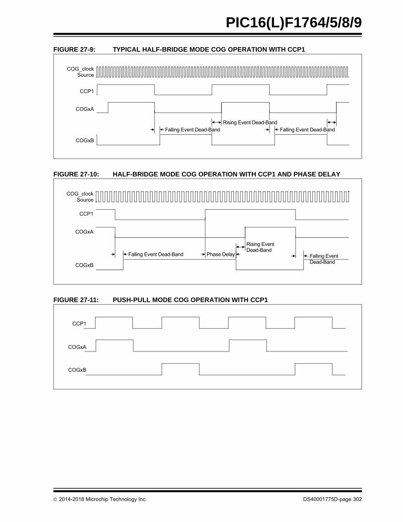
2014-2018 Microchip Technology Inc. DS40001775D-page 302
PIC16(L)F1764/5/8/9
FIGURE 27-9: TYPICAL HALF-BRIDGE MODE COG OPERATION WITH CCP1
FIGURE 27-10: HALF-BRIDGE MODE COG OPERATION WITH CCP1 AND PHASE DELAY
FIGURE 27-11: PUSH-PULL MODE COG OPERATION WITH CCP1
COG_clock
CCP1
COGxA
COGxB
Source
Falling Event Dead-BandRising Event Dead-Band
Falling Event Dead-Band
Falling Event
Rising Event
Phase DelayFalling Event Dead-Band
CCP1
COGxA
COGxB
COG_clock Source
Dead-Band
Dead-Band
CCP1
COGxA
COGxB

2014-2018 Microchip Technology Inc. DS40001775D-page 303
PIC16(L)F1764/5/8/9
FIGURE 27-12: FULL-BRIDGE FORWARD MODE COG OPERATION WITH CCP1
FIGURE 27-13: FULL-BRIDGE MODE COG OPERATION WITH CCP1 AND DIRECTION CHANGE
CCP1
COGxA
COGxB
COGxC
COGxD
CCP1
COGxA
COGxB
COGxC
COGxD
MD0
Falling Event Dead-Band

2014-2018 Microchip Technology Inc. DS40001775D-page 304
PIC16(L)F1764/5/8/9
27.4 Clock Sources
The COG_clock is used as the reference clock to thevarious timers in the peripheral. Timers that use theCOG_clock include:
• Rising and falling dead-band time• Rising and falling blanking time• Rising and falling event phase delay
Clock sources available for selection include:
• 16 MHz HFINTOSC (active during Sleep)• Instruction clock (FOSC/4)• System clock (FOSC)
The clock source is selected with the CS<1:0> bits ofthe COGxCON0 register (Register 27-1).
27.5 Selectable Event Sources
The COG uses any combination of independently select-able event sources to generate the complementarywaveform. Sources fall into two categories:
• Rising event sources• Falling event sources
The rising event sources are selected by setting bits inthe COGxRIS0 and COGxRIS1 registers (Register 27-3and Register 27-4). The falling event sources areselected by setting bits in the COGxFIS0 and COGxF1registers (Register 27-7 and Register 27-8). All selectedsources are OR’d together to generate thecorresponding event signal. Refer to Figure 27-7.
27.5.1 EDGE vs. LEVEL SENSING
Event input detection may be selected as level oredge-sensitive. The Detection mode is individually select-able for every source. Rising Source Detection modes areselected with the COGxRSIM0 and COGxRSIM1registers (Register 27-5 and Register 27-6). FallingSource Detection modes are selected with theCOGxFSIM0 and COGxFSIM1 registers (Register 27-9and Register 27-10). A set bit selects edge detection forthe corresponding event source. A cleared bit selectslevel detection.
In general, events that are driven from a periodic sourceshould be edge-detected and events that are derived fromvoltage thresholds at the target circuit should belevel-sensitive. Consider the following two examples:
1. The first example is an application in which theperiod is determined by a 50% duty cycle clock on therising event input and the COG output duty cycle isdetermined by a voltage level fed back through a com-parator on the falling event input. If the clock input islevel-sensitive, duty cycles less than 50% will exhibiterratic operation because the level-sensitive clock willsuppress the comparator feedback.
2. The second example is similar to the first exceptthat the duty cycle is close to 100%. The feedbackcomparator high-to-low transition trips the COG drive off,but almost immediately the period source turns the driveback on. If the off cycle is short enough, the comparatorinput may not reach the low side of the hysteresis bandprecluding an output change. The comparator outputstays low and without a high-to-low transition to triggerthe edge sense, the drive of the COG output will be stuckin a constant drive-on condition. See Figure 27-14.
FIGURE 27-14: EDGE vs. LEVEL SENSE
Rising (CCP1)
Falling (C1OUT)
C1IN-
COGOUT
hyst
Edge-Sensitive
Rising (CCP1)
Falling (C1OUT)
C1IN-
COGOUT
hyst
Level-Sensitive

2014-2018 Microchip Technology Inc. DS40001775D-page 305
PIC16(L)F1764/5/8/9
27.5.2 RISING EVENT
The rising event starts the PWM output active dutycycle period. The rising event is the low-to-hightransition of the rising_event output. When the risingevent phase delay and dead-band time values are zero,the primary output starts immediately. Otherwise, theprimary output is delayed. The rising event sourcecauses all the following actions:
• Start rising event phase delay counter (if enabled)• Clear complementary output after phase delay• Start falling event input blanking (if enabled)• Start dead-band delay (if enabled)• Set primary output after dead-band delay expires
27.5.3 FALLING EVENT
The falling event terminates the PWM output active dutycycle period. The falling event is the high-to-lowtransition of the falling_event output. When the fallingevent phase delay and dead-band time values are zero,the complementary output starts immediately. Otherwise,the complementary output is delayed. The falling eventsource causes all the following actions:
• Start falling event phase delay counter (if enabled)
• Clear primary output• Start rising event input blanking (if enabled)• Start falling event dead-band delay (if enabled)• Set complementary output after dead-band delay
expires
27.6 Output Control
Upon disabling, or immediately after enabling the COGmodule, the primary COG outputs are inactive andcomplementary COG outputs are active.
27.6.1 OUTPUT ENABLES
There are no output enable controls in the COGmodule. Instead, each device pin has an individualoutput selection control called the PPS register. Allfour COG outputs are available for selection in thePPS register of every pin.
When a COG output is enabled by PPS selection, theoutput on the pin has several possibilities which dependon the mode, steering control, EN bit and shutdownstate, as shown in Table 27-1 and Table 27-2.
.
27.6.2 POLARITY CONTROL
The polarity of each COG output can be selectedindependently. When the output polarity bit is set, thecorresponding output is active-low. Clearing the outputpolarity bit configures the corresponding output asactive-high. However, polarity affects the outputs inonly one of the four Shutdown Override modes. SeeSection 27.10 “Auto-Shutdown Control” for moredetails.
Output polarity is selected with the POLA through POLDbits of the COGxCON1 register (Register 27-2).
27.7 Dead-Band Control
The dead-band control provides for non-overlappingPWM output signals to prevent shoot-through currentin the external power switches. Dead-band timeaffects the output only in the Half-Bridge mode andwhen changing direction in the Full-Bridge mode.
The COG contains two dead-band timers. Onedead-band timer is used for rising event dead-bandcontrol. The other is used for falling event dead-bandcontrol. Timer modes are selectable as either:
• Asynchronous delay chain• Synchronous counter
The Dead-Band Timer mode is selected for the risingevent and falling event dead-band times, with therespective RDBS and FDBS bits of the COGxCON1register (Register 27-2).
In Half-Bridge mode, the rising event dead-band timedelays all selected primary outputs from going activefor the selected dead-band time after the rising event.COGxA and COGxC are the primary outputs inHalf-Bridge mode.
In Half-Bridge mode, the falling event dead-band timedelays all selected complementary outputs from goingactive for the selected dead-band time after the fallingevent. COGxB and COGxD are the complementaryoutputs in Half-Bridge mode.
In Full-Bridge mode, the dead-band delay occurs onlyduring direction changes. The modulated output isdelayed for the falling event dead-band time after adirection change from forward to reverse. The modulatedoutput is delayed for the rising event dead-band time aftera direction change from reverse to forward.
TABLE 27-1: PIN OUTPUT STATES MD<2:0> = 00x
EN Bit STR Bit Shutdown Output
x 0 Inactive Static Steering Data
x 1 Active Shutdown Override
0 1 Inactive Inactive State
1 1 Inactive Active PWM Signal
TABLE 27-2: PIN OUTPUT STATES MD<2:0> > 001
EN Bit STR Bit Shutdown Output
x x Inactive Inactive State
x x Active Shutdown Override
1 x Inactive Active PWM Signal
2014-2018 Microchip Technology Inc. DS40001775D-page 306
PIC16(L)F1764/5/8/9
27.7.1 ASYNCHRONOUS DELAY CHAIN DEAD-BAND DELAY
Asynchronous dead-band delay is determined by thetime it takes the input to propagate through a series ofdelay elements. Each delay element is a nominal fivenanoseconds.
For rising event asynchronous dead-band delay, setthe RDBS bit of the COGxCON0 register and set theCOGxDBR register (Register 27-14) value to thedesired number of delay elements in the rising eventdead-band time.
For falling event asynchronous dead-band delay, setthe FDBS bit of the COGxCON0 register and set theCOGxDBF register (Register 27-15) value to thedesired number of delay elements in the falling eventdead-band time.
Setting the value to zero disables dead-band delay.
27.7.2 SYNCHRONOUS COUNTER DEAD-BAND DELAY
Synchronous counter dead-band is timed by countingCOG_clock periods from zero, up to the value in theDead-Band Count register. Use Equation 27-1 tocalculate dead-band times.
For rising event synchronous dead-band delay, clearthe RDBS bit of the COGxCON0 register and set theCOGxDBR register value to the number of COG_clockperiods in the rising event dead-band time.
For falling event synchronous dead-band delay, clearthe FDBS bit of the COGxCON0 register and set theCOGxDBF register value to the number of COG_clockperiods in the falling event dead-band time.
When the value is zero, dead-band delay is disabled.
27.7.3 SYNCHRONOUS COUNTER DEAD-BAND TIME UNCERTAINTY
When the rising and falling events that trigger thedead-band counters come from asynchronous inputs,it creates uncertainty in the synchronous counterdead-band time. The maximum uncertainty is equal toone COG_clock period. Refer to Example 27-1 formore detail.
When event input sources are asynchronous with nophase delay, use the Asynchronous Delay ChainDead-Band mode to avoid the dead-band timeuncertainty.
27.7.4 RISING EVENT DEAD-BAND
Rising event dead-band delays the turn-on of theprimary outputs from when complementary outputs areturned off. The rising event dead-band time startswhen the rising_ event output goes true.
See Section 27.7.1 “Asynchronous Delay ChainDead-Band Delay” and Section 27.7.2 “SynchronousCounter Dead-Band Delay” for more information onsetting the rising edge dead-band time.
27.7.5 FALLING EVENT DEAD-BAND
Falling event dead-band delays the turn-on ofcomplementary outputs from when the primary outputsare turned off. The falling event dead-band time startswhen the falling_event output goes true.
See Section 27.7.1 “Asynchronous Delay ChainDead-Band Delay” and Section 27.7.2 “SynchronousCounter Dead-Band Delay” for more information onsetting the rising edge dead-band time.
27.7.6 DEAD-BAND OVERLAP
There are two cases of potential dead-band overlap:
• Rising-to-falling• Falling-to-rising
27.7.6.1 Rising-to-Falling Overlap
In this case, the falling event occurs while the risingevent dead-band counter is still counting. When thishappens, the primary drives are suppressed and thedead-band extends by the falling event dead-bandtime. At the termination of the extended dead-bandtime, the complementary drive goes true.
27.7.6.2 Falling-to-Rising Overlap
In this case, the rising event occurs while the fallingevent dead-band counter is still counting. When thishappens, the complementary drive is suppressed andthe dead-band extends by the rising event dead-bandtime. At the termination of the extended dead-bandtime, the primary drive goes true.
27.8 Blanking Control
Input blanking is a function whereby the event inputscan be masked or blanked for a short period of time.This is to prevent electrical transients caused by theturn-on/off of power components from generating afalse input event.
The COG contains two blanking counters: onetriggered by the rising event and the other triggered bythe falling_event. The counters are cross coupled withthe events they are blanking. The falling eventblanking counter is used to blank rising input eventsand the rising event blanking counter is used to blankfalling input events. Once started, blanking extends forthe time specified by the corresponding blankingcounter.
Blanking is timed by counting COG_clock periods fromzero, up to the value in the Blanking Count register. UseEquation 27-1 to calculate blanking times.

2014-2018 Microchip Technology Inc. DS40001775D-page 307
PIC16(L)F1764/5/8/9
27.8.1 FALLING EVENT BLANKING OF RISING EVENT INPUTS
The falling event blanking counter inhibits rising eventinputs from triggering a rising event. The falling eventblanking time starts when the rising_event output drivegoes false.
The falling event blanking time is set by the valuecontained in the COGxBLKF register (Register 27-17).Blanking times are calculated using the formula shownin Equation 27-1.
When the COGxBLKF value is zero, falling eventblanking is disabled and the blanking counter output istrue, thereby, allowing the event signal to pass straightthrough to the event trigger circuit.
27.8.2 RISING EVENT BLANKING OF FALLING EVENT INPUTS
The rising event blanking counter inhibits falling eventinputs from triggering a falling event. The rising eventblanking time starts when the falling_event outputdrive goes false.
The rising event blanking time is set by the valuecontained in the COGxBLKR register (Register 27-16).
When the COGxBLKR value is zero, rising eventblanking is disabled and the blanking counter output istrue, thereby, allowing the event signal to pass straightthrough to the event trigger circuit.
27.8.3 BLANKING TIME UNCERTAINTY
When the rising and falling sources that trigger theblanking counters are asynchronous to theCOG_clock, it creates uncertainty in the blanking time.The maximum uncertainty is equal to one COG_clockperiod. Refer to Equation 27-1 and Example 27-1 formore detail.
27.9 Phase Delay
It is possible to delay the assertion of either, or both,the rising event and falling events. This is accom-plished by placing a non-zero value in COGxPHR orCOGxPHF phase-delay count registers, respectively(Register 27-18 and Register 27-19). Refer toFigure 27-10 for COG operation with CCP1 and phasedelay. The delay from the input rising event signalswitching to the actual assertion of the events is calcu-lated the same as the dead-band and blanking delays.Refer to Equation 27-1.
When the phase-delay count value is zero, phasedelay is disabled and the phase-delay counter outputis true, thereby, allowing the event signal to passstraight through to the complementary output driverflop.
27.9.1 CUMULATIVE UNCERTAINTY
It is not possible to create more than one COG_clock ofuncertainty by successive stages. Consider that thephase-delay stage comes after the blanking stage, thedead-band stage comes after either the blanking orphase-delay stages, and the blanking stage comesafter the dead-band stage. When the preceding stageis enabled, the output of that stage is necessarilysynchronous with the COG_clock, which removes anypossibility of uncertainty in the succeeding stage.
EQUATION 27-1: PHASE, DEAD-BAND AND BLANKING TIME CALCULATION
Note: All inputs to the COG should be treated asasynchronous for the purpose ofdetermining blanking, phase delay, anddead-band delay uncertainty. One clock ofuncertainty may occur as a result of signalpath length differences between the sourcesignal, such as a PWM output, and thesource clock, such as FOSC, even thoughthey both use the system clock as a timingsource. The uncertainty is more evident athigh frequencies and high temperature.
Work around
When possible, choose timing sourcefrequencies less than 20 MHz. Use theasynchronous delay chain fordead-band delay.
TminCount
FCOG_clock---------------------------------=
TmaxCount 1+
FCOG_clock---------------------------------=
Tuncertainty Tmax Tmin–=
Tuncertainty1
FCOG_clock---------------------------------=
Also:
Where:
T Count
Rising Phase Delay COGxPHR
Falling Phase Delay COGxPHF
Rising Dead Band COGxDBR
Falling Dead Band COGxDBF
Rising Event Blanking COGxBLKR
Falling Event Blanking COGxBLKF

2014-2018 Microchip Technology Inc. DS40001775D-page 308
PIC16(L)F1764/5/8/9
EXAMPLE 27-1: TIMER UNCERTAINTY
27.10 Auto-Shutdown Control
Auto-shutdown is a method to immediately overridethe COG output levels with specific overrides thatallow for safe shutdown of the circuit.
The shutdown state can be either cleared automati-cally or held until cleared by software. In either case,the shutdown overrides remain in effect until the firstrising event after the shutdown is cleared.
27.10.1 SHUTDOWN
The shutdown state can be entered by either of thefollowing two mechanisms:
• Software generated• External input
27.10.1.1 Software Generated Shutdown
Setting the ASE bit of the COGxASD0 register(Register 27-11) will force the COG into the shutdownstate.
When auto-restart is disabled, the shutdown state willpersist until the first rising event after the ASE bit iscleared by software.
When auto-restart is enabled, the ASE bit will clearautomatically and resume operation on the first risingevent after the shutdown input clears. SeeFigure 27-15 and Section 27.10.3.2 “Auto-Restart”.
27.10.1.2 External Shutdown Source
External shutdown inputs provide the fastest way tosafely suspend COG operation in the event of a Faultcondition. When any of the selected shutdown inputsgo true, the output drive latches are reset and theCOG outputs immediately go to the selected overridelevels without software delay.
Any combination of the input sources can be selectedto cause a shutdown condition. Shutdown occurswhen the selected source is low. Shutdown inputsources include:
• Any input pin selected with the COGxINPPS control
• Comparator 1• Comparator 2• Comparator 3• Comparator 4• CLC2 output• Timer2 output• Timer4 output
Shutdown inputs are selected independently with bitsof the COGxASD1 register (Register 27-12).
27.10.2 PIN OVERRIDE LEVELS
The levels driven to the output pins, while theshutdown is active, are controlled by the ASDAC<1:0>and ASDBC<1:0> bits of the COGxASD0 register(Register 27-11). ASDAC<1:0> controls the COGxAand COGxC override levels, and ASDBC<1:0>controls the COGxB and COGxD override levels.There are four override options for each output pair:
• Forced low• Forced high• Tri-state• PWM inactive state (same state as that caused by
a falling event)
Given:
Therefore:
Count Ah 10d= =
FCOG_Clock 8MHz=
Tuncertainty1
FCOG_clock---------------------------------=
1
8MHz---------------= 125ns=
Proof:
TminCount
FCOG_clock---------------------------------=
125ns 10d= 1.25s=
TmaxCount 1+
FCOG_clock---------------------------------=
125ns 10d 1+ =
1.375s=
Therefore:
Tuncertainty Tmax Tmin–=
1.375s 1.25s–=
125ns=
Note: Shutdown inputs are level-sensitive, notedge-sensitive. The shutdown statecannot be cleared as long as theshutdown input level persists, except bydisabling auto-shutdown,
Note: The polarity control does not apply to theforced low and high override levels butdoes apply to the PWM inactive state.

2014-2018 Microchip Technology Inc. DS40001775D-page 309
PIC16(L)F1764/5/8/9
27.10.3 AUTO-SHUTDOWN RESTART
After an auto-shutdown event has occurred, there aretwo ways to resume operation:
• Software controlled• Auto-restart
The restart method is selected with the ARSEN bit ofthe COGxASD0 register. Waveforms of a softwarecontrolled automatic restart are shown in Figure 27-15.
27.10.3.1 Software Controlled Restart
When the ARSEN bit of the COGxASD0 register iscleared, software must clear the ASE bit to restartCOG operation after an auto-shutdown event.
The COG will resume operation on the first risingevent after the ASE bit is cleared. Clearing theshutdown state requires all selected shutdown inputsto be false; otherwise, the ASE bit will remain set.
27.10.3.2 Auto-Restart
When the ARSEN bit of the COGxASD0 register isset, the COG will restart from the auto-shutdown stateautomatically.
The ASE bit will clear automatically and the COG willresume operation on the first rising event after allselected shutdown inputs go false.
2
01
4-2
01
8 M
icroch
ip T
ech
no
log
y Inc.
DS
40
00
17
75
D-p
ag
e 3
10
PIC
16(L)F
1764/5/8/9
FIGURE 27-15: AUTO-SHUTDOWN WAVEFORM – CCP1 AS RISING AND FALLING EVENT INPUT SOURCE
1 2 3 4 5
Next Rising Event
Next Rising Event
Cleared in Software
Cleared in Hardware
NORMAL OUTPUT SHUTDOWN NORMAL OUTPUT SHUTDOWN NORMAL OUTPUT
SOFTWARE CONTROLLED RESTART AUTO-RESTART
CCP1
ARSEN
Shutdown Input
ASE
ASDAC
ASDBD
COGxA
COGxB
Operating State
2b00
2b00 2b00

2014-2018 Microchip Technology Inc. DS40001775D-page 311
PIC16(L)F1764/5/8/9
27.11 Buffer Updates
Changes to the Phase, Dead-Band and BlankingCount registers need to occur simultaneously duringCOG operation to avoid unintended operation thatmay occur as a result of delays between each registerwrite. This is accomplished with the LD bit of theCOGxCON0 register and double-buffering of thePhase, Blanking and Dead-Band Count registers.
Before the COG module is enabled, writing the Countregisters loads the count buffers without need of theLD bit. However, when the COG is enabled, the countbuffer updates are suspended after writing the Countregisters until after the LD bit is set. When the LD bit isset, the Phase, Dead-Band and Blanking registervalues are transferred to the corresponding bufferssynchronous with COG operation. The LD bit iscleared by hardware when the transfer is complete.
27.12 Input and Output Pin Selection
The COG has one selection for an input from a devicepin. That one input can be used as rising and fallingevent source or a Fault source. The COGxINPPS reg-ister is used to select the pin. Refer to registers,xxxPPS (Register 12-1) and RxyPPS (Register 12-2).
The Pin PPS Control registers are used to enable theCOG outputs. Any combination of outputs to pins ispossible including multiple pins for the same output.See the RxyPPS control register and Section 12.2“PPS Outputs” for more details.
27.13 Operation During Sleep
The COG continues to operate in Sleep provided thatthe COG_clock, rising event, and falling event sourcesremain active.
The HFINTSOC remains active during Sleep when theCOG is enabled and the HFINTOSC is selected as theCOG_clock source.
27.14 Configuring the COG
The following steps illustrate how to properly configurethe COG to ensure a synchronous start with the risingevent input:
1. If a pin is to be used for the COG Fault or eventinput, use the COGxINPPS register to configurethe desired pin.
2. Clear all ANSELx register bits associated withpins that are used for COG functions.
3. Ensure that the TRISx control bits correspond-ing to the COG outputs to be used are set so thatall are configured as inputs. The COG modulewill enable the output drivers as needed later.
4. Clear the EN bit, if not already cleared.
5. Set desired dead-band times with theCOGxDBR and COGxDBF registers, and selectthe source with the RDBS and FDBS bits of theCOGxCON1 register.
6. Set desired blanking times with the COGxBLKRand COGxBLKF registers.
7. Set desired phase delay with the COGxPHRand COGxPHF registers.
8. Select the desired shutdown sources with theCOGxASD1 register.
9. Setup the following controls in the COGxASD0Auto-Shutdown register:
• Select both output override controls to the desired levels (this is necessary, even if not using auto-shutdown because start-up will be from a shutdown state).
• Set the ASE bit and clear the ARSEN bit.
10. Select the desired rising and falling eventsources with the COGxRIS0, COGxRIS1,COGxFIS0 and COGxFIS1 registers.
11. Select the desired Rising and Falling Eventmodes with the COGxRSIM0, COGxRSIMI1,COGxFSIM0 and COGxFSIM1 registers.
12. Configure the following controls in theCOGxCON1 register:
• Set the polarity for each output• Select the desired dead-band timing sources
13. Configure the following controls in theCOGxCON0 register:
• Set the desired operating mode• Select the desired clock source
14. If one of the Steering modes is selected, thenconfigure the following controls in theCOGxSTR register:
• Set the steering bits of the outputs to be used.
• Set the desired static levels.
15. Set the EN bit.
16. Set the pin PPS controls to direct the COGoutputs to the desired pins.
17. If auto-restart is to be used, set the ARSEN bitand the ASE will be cleared automatically;otherwise, clear the ASE bit to start the COG.

2014-2018 Microchip Technology Inc. DS40001775D-page 312
PIC16(L)F1764/5/8/9
27.15 Register Definitions: COG Control
Long bit name prefixes for the COG peripherals areshown in Table 27-3. Refer to Section 1.1 “Registerand Bit Naming Conventions” for more information.
TABLE 27-3: BIT NAME PREFIXES
Peripheral Bit Name Prefix
COG1 G1
COG2(1) G2
Note 1: PIC16(L)F1768/9 devices only.
REGISTER 27-1: COGxCON0: COGx CONTROL REGISTER 0
R/W-0/0 R/W-0/0 U-0 R/W-0/0 R/W-0/0 R/W-0/0 R/W-0/0 R/W-0/0
EN LD — CS<1:0> MD<2:0>
bit 7 bit 0
Legend:
R = Readable bit W = Writable bit
u = Bit is unchanged x = Bit is unknown U = Unimplemented bit, read as ‘0’
‘1’ = Bit is set ‘0’ = Bit is cleared -n/n = Value at POR and BOR/Value at all other Resets
bit 7 EN: COGx Enable bit
1 = Module is enabled0 = Module is disabled
bit 6 LD: COGx Load Buffers bit
1 = Phase, blanking and dead-band buffers to be loaded with register values on next input events0 = Register to buffer transfer is complete
bit 5 Unimplemented: Read as ‘0’
bit 4-3 CS<1:0>: COGx Clock Selection bits
11 = Reserved; do not use10 = COG_clock is HFINTOSC (stays active during Sleep)01 = COG_clock is FOSC
00 = COG_clock is FOSC/4
bit 2-0 MD<2:0>: COGx Mode Selection bits
11x = Reserved; do not use101 = COG outputs operate in Push-Pull mode100 = COG outputs operate in Half-Bridge mode011 = COG outputs operate in Reverse Full-Bridge mode010 = COG outputs operate in Forward Full-Bridge mode001 = COG outputs operate in Synchronous Steered PWM mode000 = COG outputs operate in Steered PWM mode
2014-2018 Microchip Technology Inc. DS40001775D-page 313
PIC16(L)F1764/5/8/9
REGISTER 27-2: COGxCON1: COGx CONTROL REGISTER 1
R/W-0/0 R/W-0/0 U-0 U-0 R/W-0/0 R/W-0/0 R/W-0/0 R/W-0/0
RDBS FDBS — — POLD POLC POLB POLA
bit 7 bit 0
Legend:
R = Readable bit W = Writable bit
u = Bit is unchanged x = Bit is unknown U = Unimplemented bit, read as ‘0’
‘1’ = Bit is set ‘0’ = Bit is cleared -n/n = Value at POR and BOR/Value at all other Resets
bit 7 RDBS: COGx Rising Event Dead-Band Timing Source Select bit
1 = Delay chain and COGxDBR are used for dead-band timing generation0 = COGx_clock and COGxDBR are used for dead-band timing generation
bit 6 FDBS: COGx Falling Event Dead-band Timing Source select bit
1 = Delay chain and COGxDBF are used for dead-band timing generation0 = COGx_clock and COGxDBF are used for dead-band timing generation
bit 5-4 Unimplemented: Read as ‘0’
bit 3 POLD: COGxD Output Polarity Control bit
1 = Active level of COGxD output is low0 = Active level of COGxD output is high
bit 2 POLC: COGxC Output Polarity Control bit
1 = Active level of COGxC output is low0 = Active level of COGxC output is high
bit 1 POLB: COGxB Output Polarity Control bit
1 = Active level of COGxB output is low0 = Active level of COGxB output is high
bit 0 POLA: COGxA Output Polarity Control bit
1 = Active level of COGxA output is low0 = Active level of COGxA output is high

2014-2018 Microchip Technology Inc. DS40001775D-page 314
PIC16(L)F1764/5/8/9
REGISTER 27-3: COGxRIS0: COGx RISING EVENT INPUT SELECTION REGISTER 0
R/W-0/0 R/W-0/0 R/W-0/0 R/W-0/0 R/W-0/0 R/W-0/0 R/W-0/0 R/W-0/0
RIS7 RIS6 RIS5 RIS4 RIS3 RIS2 RIS1 RIS0
bit 7 bit 0
Legend:
R = Readable bit W = Writable bit
u = Bit is unchanged x = Bit is unknown U = Unimplemented bit, read as ‘0’
‘1’ = Bit is set ‘0’ = Bit is cleared -n/n = Value at POR and BOR/Value at all other Resets
bit 7 RIS7: COGx Rising Event Input Source 7 Enable bit
1 = PWM3 output is enabled as a rising event input0 = PWM3 output has no effect on the rising event
bit 6 RIS6: COGx Rising Event Input Source 6 Enable bit
1 = CCP2 output is enabled as a rising event input0 = CCP2 output has no effect on the rising event
bit 5 RIS5: COGx Rising Event Input Source 5 Enable bit
1 = CCP1 output is enabled as a rising event input0 = CCP1 output has no effect on the rising event
bit 4 RIS4: COGx Rising Event Input Source 4 Enable bit
1 = Comparator 4 output is enabled as a rising event input0 = Comparator 4 output has no effect on the rising event
bit 3 RIS3: COGx Rising Event Input Source 3 Enable bit
1 = Comparator 3 output is enabled as a rising event input0 = Comparator 3 output has no effect on the rising event
bit 2 RIS2: COGx Rising Event Input Source 2 Enable bit
1 = Comparator 2 output is enabled as a rising event input0 = Comparator 2 output has no effect on the rising event
bit 1 RIS1: COGx Rising Event Input Source 1 Enable bit
1 = Comparator 1 output is enabled as a rising event input0 = Comparator 1 output has no effect on the rising event
bit 0 RIS0: COGx Rising Event Input Source 0 Enable bit
1 = Pin selected with COGxINPPS register is enabled as rising event input0 = Pin selected with COGxINPPS register has no effect on the rising event

2014-2018 Microchip Technology Inc. DS40001775D-page 315
PIC16(L)F1764/5/8/9
REGISTER 27-4: COGxRIS1: COGx RISING EVENT INPUT SELECTION REGISTER 1
R/W-0/0 R/W-0/0 R/W-0/0 R/W-0/0 R/W-0/0 R/W-0/0 R/W-0/0 R/W-0/0
RIS15(1) RIS14 RIS13 RIS12 RIS11 RIS10 RIS9 RIS8
bit 7 bit 0
Legend:
R = Readable bit W = Writable bit
u = Bit is unchanged x = Bit is unknown U = Unimplemented bit, read as ‘0’
‘1’ = Bit is set ‘0’ = Bit is cleared -n/n = Value at POR and BOR/Value at all other Resets
bit 7 RIS15: COGx Rising Event Input Source 15 Enable bit(1)
1 = DSM2 MD2_out is enabled as a rising event input0 = DSM2 MD2_out has no effect on the rising event
bit 6 RIS14: COGx Rising Event Input Source 14 Enable bit
1 = DSM1 MD1_out output is enabled as a rising event input0 = DSM1 MD1_out has no effect on the rising event
bit 5 RIS13: COGx Rising Event Input Source 13 Enable bit
1 = CLC3 output is enabled as a rising event input0 = CLC3 output has no effect on the rising event
bit 4 RIS12: COGx Rising Event Input Source 12 Enable bit
1 = CLC2 output is enabled as a rising event input0 = CLC2 output has no effect on the rising event
bit 3 RIS11: COGx Rising Event Input Source 11 Enable bit
1 = CLC1 output is enabled as a rising event input0 = CLC1 output has no effect on the rising event
bit 2 RIS10: COGx Rising Event Input Source 10 Enable bit
1 = PWM6 output is enabled as a rising event input0 = PWM6 output has no effect on the rising event
bit 1 RIS9: COGx Rising Event Input Source 9 Enable bit
1 = PWM5 output is enabled as a rising event input0 = PWM5 output has no effect on the rising event
bit 0 RIS8: COGx Rising Event Input Source 8 Enable bit
1 = PWM4 output is enabled as rising event input0 = PWM4 output has no effect on the rising event
Note 1: PIC16(L)F1768/9 only. Otherwise unimplemented, read as ‘0’.

2014-2018 Microchip Technology Inc. DS40001775D-page 316
PIC16(L)F1764/5/8/9
REGISTER 27-5: COGxRSIM0: COGx RISING EVENT SOURCE INPUT MODE REGISTER 0
R/W-0/0 R/W-0/0 R/W-0/0 R/W-0/0 R/W-0/0 R/W-0/0 R/W-0/0 R/W-0/0
RSIM7 RSIM6 RSIM5 RSIM4 RSIM3 RSIM2 RSIM1 RSIM0
bit 7 bit 0
Legend:
R = Readable bit W = Writable bit
u = Bit is unchanged x = Bit is unknown U = Unimplemented bit, read as ‘0’
‘1’ = Bit is set ‘0’ = Bit is cleared -n/n = Value at POR and BOR/Value at all other Resets
bit 7 RSIM7: COGx Rising Event Input Source 7 Mode bit
RIS7 = 1:
1 = PWM3 output low-to-high transition will cause a rising event after rising event phase delay0 = PWM3 output high level will cause an immediate rising event
RIS7 = 0:PWM3 output has no effect on rising event.
bit 6 RSIM6: COGx Rising Event Input Source 6 Mode bit
RIS6 = 1:
1 = CCP2 output low-to-high transition will cause a rising event after rising event phase delay0 = CCP2 output high level will cause an immediate rising event
RIS6 = 0:CCP2 output has no effect on rising event.
bit 5 RSIM5: COGx Rising Event Input Source 5 Mode bit
RIS5 = 1:
1 = CCP1 output low-to-high transition will cause a rising event after rising event phase delay0 = CCP1 output high level will cause an immediate rising event
RIS5 = 0:CCP1 output has no effect on rising event.
bit 4 RSIM4: COGx Rising Event Input Source 4 Mode bit
RIS4 = 1:
1 = Comparator 4 output low-to-high transition will cause a rising event after rising event phase delay0 = Comparator 4 output high level will cause an immediate rising event
RIS4 = 0:Comparator 4 has no effect on rising event.
bit 3 RSIM3: COGx Rising Event Input Source 3 Mode bit
RIS3 = 1:
1 = Comparator 3 output low-to-high transition will cause a rising event after rising event phase delay0 = Comparator 3 output high level will cause an immediate rising event
RIS3 = 0:Comparator 3 output has no effect on rising event.
bit 2 RSIM2: COGx Rising Event Input Source 2 Mode bit
RIS2 = 1:
1 = Comparator 2 output low-to-high transition will cause a rising event after rising event phase delay0 = Comparator 2 output high level will cause an immediate rising event
RIS2 = 0:Comparator 2 has no effect on rising event.

2014-2018 Microchip Technology Inc. DS40001775D-page 317
PIC16(L)F1764/5/8/9
bit 1 RSIM1: COGx Rising Event Input Source 1 Mode bit
RIS1 = 1:
1 = Comparator 1 low-to-high transition will cause a rising event after rising event phase delay0 = Comparator 1 high level will cause an immediate rising event
RIS1 = 0:Comparator 1 has no effect on rising event.
bit 0 RSIM0: COGx Rising Event Input Source 0 Mode bit
RIS0 = 1:
1 = Pin selected with COGxINPPS register low-to-high transition will cause a rising event after risingevent phase delay
0 = Pin selected with COGxINPPS register high level will cause an immediate rising event
RIS0 = 0:Pin selected with COGxINPPS register has no effect on rising event.
REGISTER 27-5: COGxRSIM0: COGx RISING EVENT SOURCE INPUT MODE REGISTER 0 (CONTINUED)

2014-2018 Microchip Technology Inc. DS40001775D-page 318
PIC16(L)F1764/5/8/9
REGISTER 27-6: COGxRSIM1: COGx RISING EVENT SOURCE INPUT MODE REGISTER 1
R/W-0/0 R/W-0/0 R/W-0/0 R/W-0/0 R/W-0/0 R/W-0/0 R/W-0/0 R/W-0/0
RSIM15(1) RSIM14 RSIM13 RSIM12 RSIM11 RSIM10 RSIM9 RSIM8
bit 7 bit 0
Legend:
R = Readable bit W = Writable bit
u = Bit is unchanged x = Bit is unknown U = Unimplemented bit, read as ‘0’
‘1’ = Bit is set ‘0’ = Bit is cleared -n/n = Value at POR and BOR/Value at all other Resets
bit 7 RSIM15: COGx Rising Event Input Source 15 Mode bit(1)
RIS15 = 1:
1 = DSM2 MD2_out output low-to-high transition will cause a rising event after rising event phase delay0 = DSM2 MD2_out output high level will cause an immediate rising event
RIS15 = 0:DSM2 MD2_out output has no effect on rising event.
bit 6 RSIM14: COGx Rising Event Input Source 14 Mode bit
RIS14 = 1:
1 = DSM1 MD1_out output low-to-high transition will cause a rising event after rising event phase delay0 = DSM1 MD1_out output high level will cause an immediate rising event
RIS14 = 0:DSM1 MD1_out output has no effect on rising event.
bit 7-6 Unimplemented: Read as ‘0’
bit 5 RSIM13: COGx Rising Event Input Source 13 Mode bit
RIS13 = 1:
1 = CLC3 output low-to-high transition will cause a rising event after rising event phase delay0 = CLC3 output high level will cause an immediate rising event
RIS13 = 0:CLC3 output has no effect on rising event.
bit 4 RSIM12: COGx Rising Event Input Source 12 Mode bit
RIS12 = 1:
1 = CLC2 output low-to-high transition will cause a rising event after rising event phase delay0 = CLC2 output high level will cause an immediate rising event
RIS12 = 0:CLC2 output has no effect on rising event.
bit 3 RSIM11: COGx Rising Event Input Source 11 Mode bit
RIS11 = 1:
1 = CLC1 output low-to-high transition will cause a rising event after rising event phase delay0 = CLC1 output high level will cause an immediate rising event
RIS11 = 0:CLC1 output has no effect on rising event.
bit 2 RSIM10: COGx Rising Event Input Source 10 Mode bit
RIS10 = 1:
1 = PWM6 output low-to-high transition will cause a rising event after rising event phase delay0 = PWM6 output high level will cause an immediate rising event
RIS10 = 0:PWM6 output has no effect on rising event.
Note 1: PIC16(L)F1768/9 only. Otherwise unimplemented, read as ‘0’.

2014-2018 Microchip Technology Inc. DS40001775D-page 319
PIC16(L)F1764/5/8/9
bit 1 RSIM9: COGx Rising Event Input Source 9 Mode bit
RIS9 = 1:
1 = PWM5 output low-to-high transition will cause a rising event after rising event phase delay0 = PWM5 output high level will cause an immediate rising event
RIS9 = 0:PWM5 output has no effect on rising event.
bit 0 RSIM8: COGx Rising Event Input Source 8 Mode bit
RIS8 = 1:
1 = PWM4 output low-to-high transition will cause a rising event after rising event phase delay0 = PWM4 output high level will cause an immediate rising event
RIS8 = 0:PWM4 output has no effect on rising event.
REGISTER 27-6: COGxRSIM1: COGx RISING EVENT SOURCE INPUT MODE REGISTER 1 (CONTINUED)
Note 1: PIC16(L)F1768/9 only. Otherwise unimplemented, read as ‘0’.

2014-2018 Microchip Technology Inc. DS40001775D-page 320
PIC16(L)F1764/5/8/9
REGISTER 27-7: COGxFIS0: COGx FALLING EVENT INPUT SELECTION REGISTER 0
R/W-0/0 R/W-0/0 R/W-0/0 R/W-0/0 R/W-0/0 R/W-0/0 R/W-0/0 R/W-0/0
FIS7 FIS6 FIS5 FIS4 FIS3 FIS2 FIS1 FIS0
bit 7 bit 0
Legend:
R = Readable bit W = Writable bit
u = Bit is unchanged x = Bit is unknown U = Unimplemented bit, read as ‘0’
‘1’ = Bit is set ‘0’ = Bit is cleared -n/n = Value at POR and BOR/Value at all other Resets
bit 7 FIS7: COGx Falling Event Input Source 7 Enable bit
1 = PWM3 output is enabled as a falling event input0 = PWM3 output has no effect on the falling event
bit 6 FIS6: COGx Falling Event Input Source 6 Enable bit
1 = CCP2 output is enabled as a falling event input0 = CCP2 output has no effect on the falling event
bit 5 FIS5: COGx Falling Event Input Source 5 Enable bit
1 = CCP1 output is enabled as a falling event input0 = CCP1 output has no effect on the falling event
bit 4 FIS4: COGx Falling Event Input Source 4 Enable bit
1 = Comparator 4 output is enabled as a falling event input0 = Comparator 4 output has no effect on the falling event
bit 3 FIS3: COGx Falling Event Input Source 3 Enable bit
1 = Comparator 3 output is enabled as a falling event input0 = Comparator 3 output has no effect on the falling event
bit 2 FIS2: COGx Falling Event Input Source 2 Enable bit
1 = Comparator 2 output is enabled as a falling event input0 = Comparator 2 output has no effect on the falling event
bit 1 FIS1: COGx Falling Event Input Source 1 Enable bit
1 = Comparator 1 output is enabled as a falling event input0 = Comparator 1 output has no effect on the falling event
bit 0 FIS0: COGx Falling Event Input Source 0 Enable bit
1 = Pin selected with COGxINPPS register is enabled as falling event input0 = Pin selected with COGxINPPS register has no effect on the falling event

2014-2018 Microchip Technology Inc. DS40001775D-page 321
PIC16(L)F1764/5/8/9
REGISTER 27-8: COGxFIS1: COGx FALLING EVENT INPUT SELECTION REGISTER 1
R/W-0/0 R/W-0/0 R/W-0/0 R/W-0/0 R/W-0/0 R/W-0/0 R/W-0/0 R/W-0/0
FIS15(1) FIS14 FIS13 FIS12 FIS11 FIS10 FIS9 FIS8
bit 7 bit 0
Legend:
R = Readable bit W = Writable bit
u = Bit is unchanged x = Bit is unknown U = Unimplemented bit, read as ‘0’
‘1’ = Bit is set ‘0’ = Bit is cleared -n/n = Value at POR and BOR/Value at all other Resets
bit 7 FIS15: COGx Falling Event Input Source 15 Mode bit(1)
1 = DSM2 MD2_out is enabled as a falling event input0 = DSM2 MD2_out has no effect on the falling event
bit 6 FIS14: COGx Falling Event Input Source 14 Mode bit
1 = DSM1 MD1_out is enabled as a falling event input0 = DSM1 MD1_out has no effect on the falling event
bit 5 FIS13: COGx Falling Event Input Source 13 Enable bit
1 = CLC3 output is enabled as a falling event input0 = CLC3 output has no effect on the falling event
bit 4 FIS12: COGx Falling Event Input Source 12 Enable bit
1 = CLC2 output is enabled as a falling event input0 = CLC2 output has no effect on the falling event
bit 3 FIS11: COGx Falling Event Input Source 11 Enable bit
1 = CLC1 output is enabled as a falling event input0 = CLC1 output has no effect on the falling event
bit 2 FIS10: COGx Falling Event Input Source 10 Enable bit
1 = PWM6 output is enabled as a falling event input0 = PWM6 output has no effect on the falling event
bit 1 FIS9: COGx Falling Event Input Source 9 Enable bit
1 = PWM5 output is enabled as a falling event input0 = PWM5 output has no effect on the falling event
bit 0 FIS8: COGx Falling Event Input Source 8 Enable bit
1 = PWM4 output is enabled as falling event input0 = PWM4 output has no effect on the falling event
Note 1: PIC16(L)F1768/9 only. Otherwise unimplemented, read as ‘0’.

2014-2018 Microchip Technology Inc. DS40001775D-page 322
PIC16(L)F1764/5/8/9
REGISTER 27-9: COGxFSIM0: COGx FALLING EVENT SOURCE INPUT MODE REGISTER 0
R/W-0/0 R/W-0/0 R/W-0/0 R/W-0/0 R/W-0/0 R/W-0/0 R/W-0/0 R/W-0/0
FSIM7 FSIM6 FSIM5 FSIM4 FSIM3 FSIM2 FSIM1 FSIM0
bit 7 bit 0
Legend:
R = Readable bit W = Writable bit
u = Bit is unchanged x = Bit is unknown U = Unimplemented bit, read as ‘0’
‘1’ = Bit is set ‘0’ = Bit is cleared -n/n = Value at POR and BOR/Value at all other Resets
bit 7 FSIM7: COGx Falling Event Input Source 7 Mode bit
FIS7 = 1:1 = PWM3 output high-to-low transition will cause a falling event after falling event phase delay0 = PWM3output low level will cause an immediate falling event
FIS7 = 0:PWM3 output has no effect on falling event.
bit 6 FSIM6: COGx Falling Event Input Source 6 Mode bit
FIS6 = 1:1 = CCP2 output high-to-low transition will cause a falling event after falling event phase delay0 = CCP2 output low level will cause an immediate falling event
FIS6 = 0:CCP2 output has no effect on falling event.
bit 5 FSIM5: COGx Falling Event Input Source 5 Mode bit
FIS5 = 1:1 = CCP1 output high-to-low transition will cause a falling event after falling event phase delay0 = CCP1 output low level will cause an immediate falling event
FIS5 = 0:CCP1 output has no effect on falling event.
bit 4 FSIM4: COGx Falling Event Input Source 4 Mode bit
FIS4 = 1:1 = Comparator 4 high-to-low transition will cause a falling event after falling event phase delay0 = Comparator 4 low level will cause an immediate falling event
FIS4 = 0:Comparator 4 has no effect on falling event.
bit 3 FSIM3: COGx Falling Event Input Source 3 Mode bit
FIS3 = 1:1 = Comparator 3 high-to-low transition will cause a falling event after falling event phase delay0 = Comparator 3 low level will cause an immediate falling event
FIS3 = 0:Comparator 3 has no effect on falling event.
bit 2 FSIM2: COGx Falling Event Input Source 2 Mode bit
FIS2 = 1:1 = Comparator 2 high-to-low transition will cause a falling event after falling event phase delay0 = Comparator 2 low level will cause an immediate falling event
FIS2 = 0:Comparator 2 has no effect on falling event.

2014-2018 Microchip Technology Inc. DS40001775D-page 323
PIC16(L)F1764/5/8/9
bit 1 FSIM1: COGx Falling Event Input Source 1 Mode bit
FIS1 = 1:1 = Comparator 1 high-to-low transition will cause a falling event after falling event phase delay0 = Comparator 1 low level will cause an immediate falling event
FIS1 = 0:Comparator 1 has no effect on falling event.
bit 0 FSIM0: COGx Falling Event Input Source 0 Mode bit
FIS0 = 1:1 = Pin selected with COGxINPPS control high-to-low transition will cause a falling event after falling
event phase delay0 = Pin selected with COGxINPPS control low level will cause an immediate falling event
FIS0 = 0:Pin selected with COGxINPPS control has no effect on falling event.
REGISTER 27-9: COGxFSIM0: COGx FALLING EVENT SOURCE INPUT MODE REGISTER 0 (CONTINUED)

2014-2018 Microchip Technology Inc. DS40001775D-page 324
PIC16(L)F1764/5/8/9
REGISTER 27-10: COGxFSIM1: COGx FALLING EVENT SOURCE INPUT MODE REGISTER 1
R/W-0/0 R/W-0/0 R/W-0/0 R/W-0/0 R/W-0/0 R/W-0/0 R/W-0/0 R/W-0/0
FSIM15(1) FSIM14 FSIM13 FSIM12 FSIM11 FSIM10 FSIM9 FSIM8
bit 7 bit 0
Legend:
R = Readable bit W = Writable bit
u = Bit is unchanged x = Bit is unknown U = Unimplemented bit, read as ‘0’
‘1’ = Bit is set ‘0’ = Bit is cleared -n/n = Value at POR and BOR/Value at all other Resets
bit 7 FSIM15: COGx Falling Event Input Source 15 Mode bit(1)
FIS15 = 1:1 = DSM2 MD2_out output high-to-low transition will cause a falling event after falling event phase delay0 = DSM2 MD2_out low level will cause an immediate falling event
FIS15 = 0:DSM2 MD2_out output has no effect on falling event.
bit 6 FSIM14: COGx Falling Event Input Source 14 Mode bit
FIS14 = 1:1 = DSM1 MD1_out output high-to-low transition will cause a falling event after falling event phase delay0 = DSM1 MD1_out output low level will cause an immediate falling event
FIS14 = 0:DSM1 MD1_out output has no effect on falling event.
bit 5 FSIM13: COGx Falling Event Input Source 13 Mode bit
FIS13 = 1:1 = CLC3 output high-to-low transition will cause a falling event after falling event phase delay0 = CLC3 output low level will cause an immediate falling event
FIS13 = 0:CLC3 output has no effect on falling event.
bit 4 FSIM12: COGx Falling Event Input Source 12 Mode bit
FIS12 = 1:1 = CLC2 output high-to-low transition will cause a falling event after falling event phase delay0 = CLC2 output low level will cause an immediate falling event
FIS12 = 0:CLC2 output has no effect on falling event.
bit 3 FSIM11: COGx Falling Event Input Source 11 Mode bit
FIS11 = 1:1 = CLC1 output high-to-low transition will cause a falling event after falling event phase delay0 = CLC1 output low level will cause an immediate falling event
FIS11 = 0:CLC1 output has no effect on falling event.
bit 2 FSIM10: COGx Falling Event Input Source 10 Mode bit
FIS10 = 1:1 = PWM6 output high-to-low transition will cause a falling event after falling event phase delay0 = PWM6 output low level will cause an immediate falling event
FIS10 = 0:Comparator 2 has no effect on falling event.
Note 1: PIC16(L)F1768/9 only. Otherwise unimplemented, read as ‘0’.

2014-2018 Microchip Technology Inc. DS40001775D-page 325
PIC16(L)F1764/5/8/9
bit 1 FSIM9: COGx Falling Event Input Source 9 Mode bit
FIS9 = 1:1 = PWM5 output high-to-low transition will cause a falling event after falling event phase delay0 = PWM5 output low level will cause an immediate falling event
FIS9 = 0:PWM5 output has no effect on falling event.
bit 0 FSIM8: COGx Falling Event Input Source 8 Mode bit
FIS8 = 1:1 = PWM4 output high-to-low transition will cause a falling event after falling event phase delay0 = PWM4 output low level will cause an immediate falling event
FIS8 = 0:PWM4 output has no effect on falling event.
REGISTER 27-10: COGxFSIM1: COGx FALLING EVENT SOURCE INPUT MODE REGISTER 1 (CONTINUED)
Note 1: PIC16(L)F1768/9 only. Otherwise unimplemented, read as ‘0’.

2014-2018 Microchip Technology Inc. DS40001775D-page 326
PIC16(L)F1764/5/8/9
REGISTER 27-11: COGxASD0: COGx AUTO-SHUTDOWN CONTROL REGISTER 0
R/W-0/0 R/W-0/0 R/W-0/0 R/W-1/1 R/W-0/0 R/W-1/1 U-0 U-0
ASE ARSEN ASDBD<1:0> ASDAC<1:0> — —
bit 7 bit 0
Legend:
R = Readable bit W = Writable bit
u = Bit is unchanged x = Bit is unknown U = Unimplemented bit, read as ‘0’
‘1’ = Bit is set ‘0’ = Bit is cleared -n/n = Value at POR and BOR/Value at all other Resets
bit 7 ASE: Auto-Shutdown Event Status bit
1 = COG is in the shutdown state0 = COG is either not in the shutdown state or will exit the shutdown state on the next rising event
bit 6 ARSEN: Auto-Restart Enable bit
1 = Auto-restart is enabled0 = Auto-restart is disabled
bit 5-4 ASDBD<1:0>: COGxB and COGxD Auto-shutdown Override Level Select bits
11 = A logic ‘1’ is placed on COGxB and COGxD when shutdown is active10 = A logic ‘0’ is placed on COGxB and COGxD when shutdown is active01 = COGxB and COGxD are tri-stated when shutdown is active00 = The inactive state of the pin, including polarity, is placed on COGxB and COGxD when shutdown
is active
bit 3-2 ASDAC<1:0>: COGxA and COGxC Auto-shutdown Override Level Select bits
11 = A logic ‘1’ is placed on COGxA and COGxC when shutdown is active10 = A logic ‘0’ is placed on COGxA and COGxC when shutdown is active01 = COGxA and COGxC are tri-stated when shutdown is active00 = The inactive state of the pin, including polarity, is placed on COGxA and COGxC when shutdown
is active
bit 1-0 Unimplemented: Read as ‘0’

2014-2018 Microchip Technology Inc. DS40001775D-page 327
PIC16(L)F1764/5/8/9
REGISTER 27-12: COGxASD1: COGx AUTO-SHUTDOWN CONTROL REGISTER 1
R/W-0/0 R/W-0/0 R/W-0/0 R/W-0/0 R/W-0/0 R/W-0/0 R/W-0/0 R/W-0/0
AS7E AS6E AS5E AS4E AS3E AS2E AS1E AS0E
bit 7 bit 0
Legend:
R = Readable bit W = Writable bit U = Unimplemented bit, read as ‘0’
u = Bit is unchanged x = Bit is unknown -n/n = Value at POR and BOR/Value at all other Resets
‘1’ = Bit is set ‘0’ = Bit is cleared q = Value depends on condition
bit 7 AS7E: COGx Auto-shutdown Source Enable bit 7
1 = COGx is shutdown when Timer4_output is high0 = Timer4_output has no effect on shutdown
bit 6 AS6E: COGx Auto-shutdown Source Enable bit 6
1 = COGx is shutdown when Timer2_output is high0 = Timer2_output has no effect on shutdown
bit 5 AS5E: COGx Auto-shutdown Source Enable bit 5
1 = COGx is shutdown when CLC LC2_out is low0 = CLC2 output has no effect on shutdown
bit 4 AS4E: COGx Auto-shutdown Source Enable bit 4
1 = COGx is shutdown when Comparator sync_C4OUT is low0 = Comparator 4 output has no effect on shutdown
bit 3 AS3E: COGx Auto-shutdown Source Enable bit 3
1 = COGx is shutdown when Comparator sync_C3OUT is low0 = Comparator 3 output has no effect on shutdown
bit 2 AS2E: COGx Auto-shutdown Source Enable bit 2
1 = COGx is shutdown when Comparator sync_C2OUT is low0 = Comparator 2 output has no effect on shutdown
bit 1 AS1E: COGx Auto-shutdown Source Enable bit 1
1 = COGx is shutdown when comparator sync_C1OUT is low0 = Comparator 1 output has no effect on shutdown
bit 0 AS0E: COGx Auto-shutdown Source Enable bit 0
1 = COGx is shutdown when pin selected with COGxINPPS register is low0 = Pin selected with COGxINPPS register has no effect on shutdown

2014-2018 Microchip Technology Inc. DS40001775D-page 328
PIC16(L)F1764/5/8/9
REGISTER 27-13: COGxSTR: COGx STEERING CONTROL REGISTER 1(1)
R/W-0/0 R/W-0/0 R/W-0/0 R/W-0/0 R/W-0/0 R/W-0/0 R/W-0/0 R/W-0/0
SDATD SDATC SDATB SDATA STRD STRC STRB STRA
bit 7 bit 0
Legend:
R = Readable bit W = Writable bit
u = Bit is unchanged x = Bit is unknown U = Unimplemented bit, read as ‘0’
‘1’ = Bit is set ‘0’ = Bit is cleared -n/n = Value at POR and BOR/Value at all other Resets
bit 7 SDATD: COGxD Static Output Data bit
1 = COGxD static data is high0 = COGxD static data is low
bit 6 SDATC: COGxC Static Output Data bit
1 = COGxC static data is high0 = COGxC static data is low
bit 5 SDATB: COGxB Static Output Data bit
1 = COGxB static data is high0 = COGxB static data is low
bit 4 SDATA: COGxA Static Output Data bit
1 = COGxA static data is high0 = COGxA static data is low
bit 3 STRD: COGxD Steering Control bit
1 = COGxD output has the COGxD waveform with polarity control from the POLD bit0 = COGxD output is the static data level determined by the SDATD bit
bit 2 STRC: COGxC Steering Control bit
1 = COGxC output has the COGxC waveform with polarity control from the POLC bit0 = COGxC output is the static data level determined by the SDATC bit
bit 1 STRB: COGxB Steering Control bit
1 = COGxB output has the COGxB waveform with polarity control from the POLB bit0 = COGxB output is the static data level determined by the SDATB bit
bit 0 STRA: COGxA Steering Control bit
1 = COGxA output has the COGxA waveform with polarity control from the POLA bit0 = COGxA output is the static data level determined by the SDATA bit
Note 1: Steering is active only when the MD<2:0> bits of the COGxCON0 register = 00x (see Register 27-1).
2014-2018 Microchip Technology Inc. DS40001775D-page 329
PIC16(L)F1764/5/8/9
REGISTER 27-14: COGxDBR: COGx RISING EVENT DEAD-BAND COUNT REGISTER
U-0 U-0 R/W-0/0 R/W-0/0 R/W-0/0 R/W-0/0 R/W-0/0 R/W-0/0
— — DBR<5:0>
bit 7 bit 0
Legend:
R = Readable bit W = Writable bit
u = Bit is unchanged x = Bit is unknown U = Unimplemented bit, read as ‘0’
‘1’ = Bit is set ‘0’ = Bit is cleared -n/n = Value at POR and BOR/Value at all other Resets
bit 7-6 Unimplemented: Read as ‘0’
bit 5-0 DBR<5:0>: Rising Event Dead-Band Count Value bits
RDBS = 0: = Number of COGx clock periods to delay primary output after rising event
RDBS = 1: = Number of delay chain element periods to delay primary output after rising event
REGISTER 27-15: COGxDBF: COGx FALLING EVENT DEAD-BAND COUNT REGISTER
U-0 U-0 R/W-0/0 R/W-0/0 R/W-0/0 R/W-0/0 R/W-0/0 R/W-0/0
DBF<5:0>
bit 7 bit 0
Legend:
R = Readable bit W = Writable bit
u = Bit is unchanged x = Bit is unknown U = Unimplemented bit, read as ‘0’
‘1’ = Bit is set ‘0’ = Bit is cleared -n/n = Value at POR and BOR/Value at all other Resets
bit 7-6 Unimplemented: Read as ‘0’
bit 5-0 DBF<5:0>: Falling Event Dead-Band Count Value bits
FDBS = 0: = Number of COGx clock periods to delay complementary output after falling event input
FDBS = 1: = Number of delay chain element periods to delay complementary output after falling event input

2014-2018 Microchip Technology Inc. DS40001775D-page 330
PIC16(L)F1764/5/8/9
REGISTER 27-16: COGxBLKR: COGx RISING EVENT BLANKING COUNT REGISTER
U-0 U-0 R/W-x/u R/W-x/u R/W-x/u R/W-x/u R/W-x/u R/W-x/u
BLKR<5:0>
bit 7 bit 0
Legend:
R = Readable bit W = Writable bit
u = Bit is unchanged x = Bit is unknown U = Unimplemented bit, read as ‘0’
‘1’ = Bit is set ‘0’ = Bit is cleared -n/n = Value at POR and BOR/Value at all other Resets
bit 7-6 Unimplemented: Read as ‘0’
bit 5-0 BLKR<5:0>: Rising Event Blanking Count Value bits
= Number of COGx clock periods to inhibit falling event inputs
REGISTER 27-17: COGxBLKF: COGx FALLING EVENT BLANKING COUNT REGISTER
U-0 U-0 R/W-0/0 R/W-0/0 R/W-0/0 R/W-0/0 R/W-0/0 R/W-0/0
BLKF<5:0>
bit 7 bit 0
Legend:
R = Readable bit W = Writable bit
u = Bit is unchanged x = Bit is unknown U = Unimplemented bit, read as ‘0’
‘1’ = Bit is set ‘0’ = Bit is cleared -n/n = Value at POR and BOR/Value at all other Resets
bit 7-6 Unimplemented: Read as ‘0’
bit 5-0 BLKF<5:0>: Falling Event Blanking Count Value bits
= Number of COGx clock periods to inhibit rising event inputs
REGISTER 27-18: COGxPHR: COGx RISING EVENT PHASE DELAY COUNT REGISTER
U-0 U-0 R/W-0/0 R/W-0/0 R/W-0/0 R/W-0/0 R/W-0/0 R/W-0/0
— — PHR<5:0>
bit 7 bit 0
Legend:
R = Readable bit W = Writable bit
u = Bit is unchanged x = Bit is unknown U = Unimplemented bit, read as ‘0’
‘1’ = Bit is set ‘0’ = Bit is cleared -n/n = Value at POR and BOR/Value at all other Resets
bit 7-6 Unimplemented: Read as ‘0’
bit 5-0 PHR<5:0>: Rising Event Phase Delay Count Value bits
= Number of COGx clock periods to delay rising event
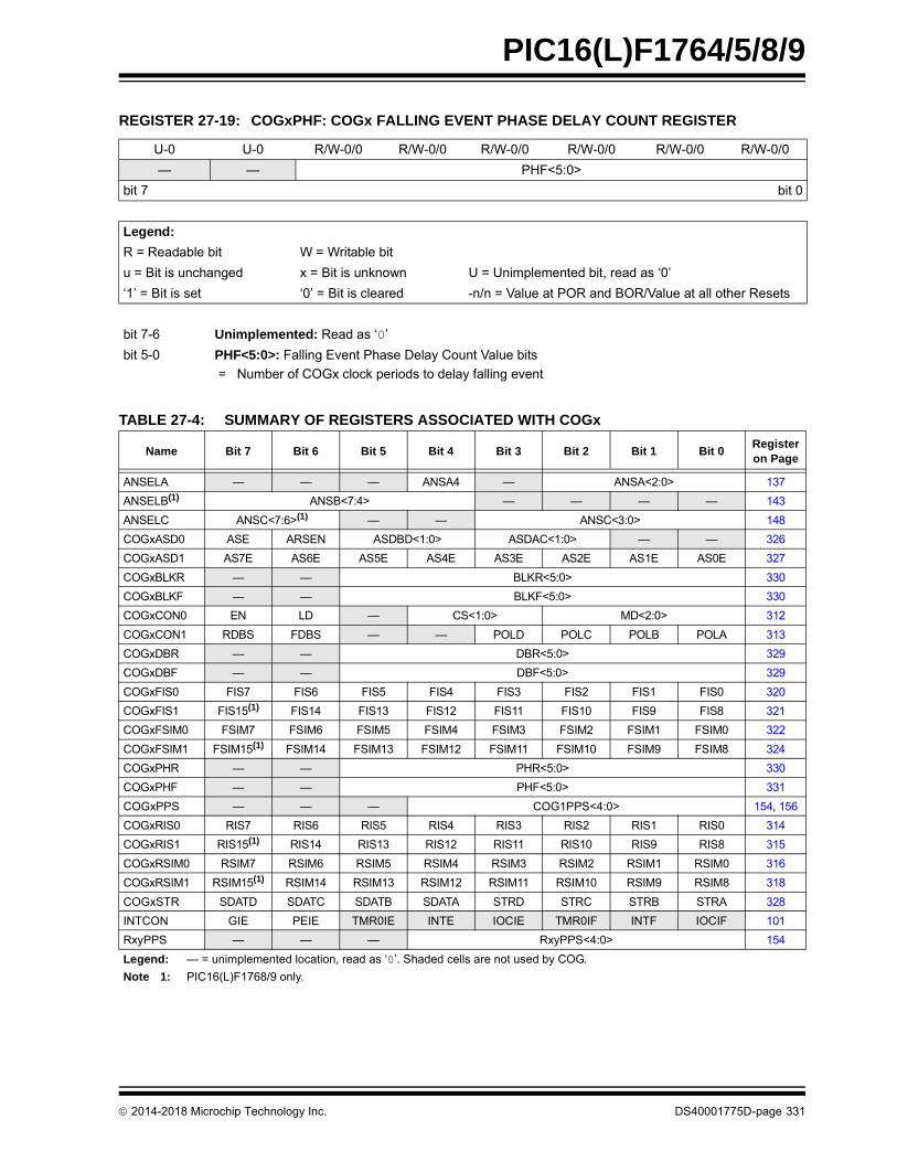
2014-2018 Microchip Technology Inc. DS40001775D-page 331
PIC16(L)F1764/5/8/9
REGISTER 27-19: COGxPHF: COGx FALLING EVENT PHASE DELAY COUNT REGISTER
U-0 U-0 R/W-0/0 R/W-0/0 R/W-0/0 R/W-0/0 R/W-0/0 R/W-0/0
— — PHF<5:0>
bit 7 bit 0
Legend:
R = Readable bit W = Writable bit
u = Bit is unchanged x = Bit is unknown U = Unimplemented bit, read as ‘0’
‘1’ = Bit is set ‘0’ = Bit is cleared -n/n = Value at POR and BOR/Value at all other Resets
bit 7-6 Unimplemented: Read as ‘0’
bit 5-0 PHF<5:0>: Falling Event Phase Delay Count Value bits
= Number of COGx clock periods to delay falling event
TABLE 27-4: SUMMARY OF REGISTERS ASSOCIATED WITH COGx
Name Bit 7 Bit 6 Bit 5 Bit 4 Bit 3 Bit 2 Bit 1 Bit 0Register on Page
ANSELA — — — ANSA4 — ANSA<2:0> 137
ANSELB(1) ANSB<7:4> — — — — 143
ANSELC ANSC<7:6>(1) — — ANSC<3:0> 148
COGxASD0 ASE ARSEN ASDBD<1:0> ASDAC<1:0> — — 326
COGxASD1 AS7E AS6E AS5E AS4E AS3E AS2E AS1E AS0E 327
COGxBLKR — — BLKR<5:0> 330
COGxBLKF — — BLKF<5:0> 330
COGxCON0 EN LD — CS<1:0> MD<2:0> 312
COGxCON1 RDBS FDBS — — POLD POLC POLB POLA 313
COGxDBR — — DBR<5:0> 329
COGxDBF — — DBF<5:0> 329
COGxFIS0 FIS7 FIS6 FIS5 FIS4 FIS3 FIS2 FIS1 FIS0 320
COGxFIS1 FIS15(1) FIS14 FIS13 FIS12 FIS11 FIS10 FIS9 FIS8 321
COGxFSIM0 FSIM7 FSIM6 FSIM5 FSIM4 FSIM3 FSIM2 FSIM1 FSIM0 322
COGxFSIM1 FSIM15(1) FSIM14 FSIM13 FSIM12 FSIM11 FSIM10 FSIM9 FSIM8 324
COGxPHR — — PHR<5:0> 330
COGxPHF — — PHF<5:0> 331
COGxPPS — — — COG1PPS<4:0> 154, 156
COGxRIS0 RIS7 RIS6 RIS5 RIS4 RIS3 RIS2 RIS1 RIS0 314
COGxRIS1 RIS15(1) RIS14 RIS13 RIS12 RIS11 RIS10 RIS9 RIS8 315
COGxRSIM0 RSIM7 RSIM6 RSIM5 RSIM4 RSIM3 RSIM2 RSIM1 RSIM0 316
COGxRSIM1 RSIM15(1) RSIM14 RSIM13 RSIM12 RSIM11 RSIM10 RSIM9 RSIM8 318
COGxSTR SDATD SDATC SDATB SDATA STRD STRC STRB STRA 328
INTCON GIE PEIE TMR0IE INTE IOCIE TMR0IF INTF IOCIF 101
RxyPPS — — — RxyPPS<4:0> 154
Legend: — = unimplemented location, read as ‘0’. Shaded cells are not used by COG.
Note 1: PIC16(L)F1768/9 only.

2014-2018 Microchip Technology Inc. DS40001775D-page 332
PIC16(L)F1764/5/8/9
28.0 CONFIGURABLE LOGIC CELL (CLC)
The Configurable Logic Cell (CLC) provides program-mable logic that operates outside the speed limitationsof software execution. The logic cell takes up to32 input signals, and through the use of configurablegates, reduces the 32 inputs to four logic lines that driveone of eight selectable single output logic functions.
Input sources are a combination of the following:
• I/O pins
• Internal clocks
• Peripherals
• Register bits
The output can be directed internally to peripherals andto an output pin.
Refer to Figure 28-1 for a simplified diagram showingsignal flow through the CLCx.
Possible configurations include:
• Combinatorial Logic:
- AND
- NAND
- AND-OR
- AND-OR-INVERT
- OR-XOR
- OR-XNOR
• Latches:
- S-R
- Clocked D with Set and Reset
- Transparent D with Set and Reset
- Clocked J-K with Reset
FIGURE 28-1: CLCx SIMPLIFIED BLOCK DIAGRAM
Inpu
t Dat
a Se
lect
ion
Gat
es(1
)
LogicFunction
(2)
g2
g1
g3
g4
MODE<2:0>
q
EN
POL
det
Interrupt
det
Interrupt
set bitCLCxIFINTN
INTP
CLCx
to Peripherals
Q1
LCx_out
LCxOUTMLCxOUTD Q
PPS
LCx_in[0]LCx_in[1]LCx_in[2]
LCx_in[35]LCx_in[36]LCx_in[37]
.
.
.
Rev. 10-000 025D6/4/201 4
CLCxPPS
TRIS
See Table 28-1.
Note 1: See Figure 28-2: Input Data Selection and Gating.
2: See Figure 28-3: Programmable Logic Functions.

2014-2018 Microchip Technology Inc. DS40001775D-page 333
PIC16(L)F1764/5/8/9
28.1 CLCx Setup
Programming the CLCx module is performed by config-uring the four stages in the logic signal flow. The fourstages are:
• Data selection
• Data gating
• Logic function selection
• Output polarity
Each stage is set up at run time by writing to the corre-sponding CLCx Special Function Registers. This hasthe added advantage of permitting logic reconfigurationon-the-fly during program execution.
28.1.1 DATA SELECTION
There are 32 signals available as inputs to the configu-rable logic. Four 32-input multiplexers are used toselect the inputs to pass on to the next stage.
Data selection is through four multiplexers, as indicatedon the left side of Figure 28-2. Data inputs in the figureare identified by a generic numbered input name.
Table 28-1 correlates the generic input name to theactual signal for each CLC module. The column labeled,dy, indicates the MUX selection code for the selecteddata input. DxS is an abbreviation for the MUX selectinput codes: D1S<5:0> through D4S<5:0>.
Data inputs are selected with the CLCxSEL0 throughCLCxSEL3 registers (Register 28-3 throughRegister 28-6).
TABLE 28-1: CLCx DATA INPUT SELECTION
Note: Data selections are undefined at power-up.
Data Inputdy
DxS<5:0>CLCx
LCx_in[38] 100110 MD1_out(1) or MD2_out(2) or Reserved(3)
LCx_in[37] 100101 FOSC
LCx_in[36] 100100 HFINTOSC
LCx_in[35] 100011 LFINTOSC
LCx_in[34] 100010 FRC (ADC RC clock)
LCx_in[33] 100001 IOCIF Set
LCx_in[32] 100000 Timer6_postscaled
LCx_in[31] 011111 Timer4_postscaled
LCx_in[30] 011110 Timer2_postscaled
LCx_in[29] 011101 Timer5 Overflow
LCx_in[28] 011100 Timer3 Overflow
LCx_in[27] 011011 Timer1 Overflow
LCx_in[26] 011010 Timer0 Overflow
LCx_in[25] 011001 EUSART RX
LCx_in[24] 011000 EUSART TX
LCx_in[23] 010111 ZCD1_output
LCx_in[22] 010110 MSSP1 SDO/SDA
LCx_in[21] 010101 MSSP1 SCL/SCK
LCx_in[20] 010100 PWM6_out
LCx_in[19] 010011 PWM5_out
LCx_in[18] 010010 PWM4_out
LCx_in[17] 010001 PWM3_out
LCx_in[16] 010000 CCP2_out
LCx_in[15] 001111 CCP1_out
LCx_in[14] 001110 COG2B
LCx_in[13] 001101 COG2A
LCx_in[12] 001100 COG1B
LCx_in[11] 001011 COG1A
LCx_in[10] 001010 sync_C4OUT
LCx_in[9] 001001 sync_C3OUT
LCx_in[8] 001000 sync_C2OUT
LCx_in[7] 000111 sync_C1OUT
LCx_in[6] 000110 LC3_out from the CLC3
LCx_in[5] 000101 LC2_out from the CLC2
LCx_in[4] 000100 LC1_out from the CLC1
LCx_in[3] 000011 CLCIN3 Pin Input Selected in CLCIN3PPS Register
LCx_in[2] 000010 CLCIN2 Pin Input Selected in CLCIN2PPS Register
LCx_in[1] 000001 CLCIN1 Pin Input Selected in CLCIN1PPS Register
LCx_in[0] 000000 CLCIN0 Pin Input Selected in CLCIN0PPS Register
Note 1: CLCxSEL0 only.2: PIC16(L)F1768/9 CLCxSEL1 only.3: CLCxSEL2, CLCxSEL3 and
PIC16(L)F1764/5 CLCxSEL1 only.

2014-2018 Microchip Technology Inc. DS40001775D-page 334
PIC16(L)F1764/5/8/9
28.1.2 DATA GATING
Outputs from the input multiplexers are directed to thedesired logic function input through the data gatingstage. Each data gate can direct any combination of thefour selected inputs.
The gate stage is more than just signal direction. Thegate can be configured to direct each input signal asinverted or non-inverted data. Directed signals areANDed together in each gate. The output of each gatecan be inverted before going on to the logic functionstage.
The gating is, in essence, a 1-to-4 inputAND/NAND/OR/NOR gate. When every input isinverted and the output is inverted, the gate is an OR ofall enabled data inputs. When the inputs and output arenot inverted, the gate is an AND or all enabled inputs.
Table 28-2 summarizes the basic logic that can beobtained in Gate 1 by using the gate logic select bits.The table shows the logic of four input variables, buteach gate can be configured to use less than four. If noinputs are selected, the output will be zero or one,depending on the gate output polarity bit.
It is possible (but not recommended) to select both thetrue and negated values of an input. When this is done,the gate output is zero, regardless of the other inputs,but may emit logic glitches (transient-induced pulses).If the output of the channel must be zero or one, therecommended method is to set all gate bits to zero anduse the gate polarity bit to set the desired level.
Data gating is configured with the Logic Gate Selectregisters as follows:
• Gate 1: CLCxGLS0 (Register 28-7)
• Gate 2: CLCxGLS1 (Register 28-8)
• Gate 3: CLCxGLS2 (Register 28-9)
• Gate 4: CLCxGLS3 (Register 28-10)
Register number suffixes are different than the gatenumbers because other variations of this module havemultiple gate selections in the same register.
Data gating is indicated in the right side of Figure 28-2.Only one gate is shown in detail. The remaining threegates are configured identically with the exception thatthe data enables correspond to the enables for thatgate.
28.1.3 LOGIC FUNCTION
There are eight available logic functions including:
• AND-OR
• OR-XOR
• AND
• S-R Latch
• D Flip-Flop with Set and Reset
• D Flip-Flop with Reset
• J-K Flip-Flop with Reset
• Transparent Latch with Set and Reset
Logic functions are shown in Figure 28-3. Each logicfunction has four inputs and one output. The four inputsare the four data gate outputs of the previous stage.The output is fed to the inversion stage and from thereto other peripherals, an output pin, and back to theCLCx itself.
28.1.4 OUTPUT POLARITY
The last stage in the Configurable Logic Cell is theoutput polarity. Setting the POL bit of the CLCxCONregister inverts the output signal from the logic stage.Changing the polarity while the interrupts are enabledwill cause an interrupt for the resulting output transition.
Note: Data gating is undefined at power-up.
TABLE 28-2: DATA GATING LOGIC
CLCxGLS0 G1POL Gate Logic
0x55 1 AND
0x55 0 NAND
0xAA 1 NOR
0xAA 0 OR
0x00 0 Logic ‘0’
0x00 1 Logic ‘1’

2014-2018 Microchip Technology Inc. DS40001775D-page 335
PIC16(L)F1764/5/8/9
28.1.5 CLCx SETUP STEPS
The following steps should be followed when setting upthe CLCx:
• Disable CLCx by clearing the EN bit.
• Select desired inputs using CLCxSEL0 through CLCxSEL3 registers (see Table 28-1).
• Clear any associated ANSELx bits.• Set all TRISx bits associated with inputs.
• Clear all TRISx bits associated with outputs.
• Enable the chosen inputs through the four gates using CLCxGLS0, CLCxGLS1, CLCxGLS2, and CLCxGLS3 registers.
• Select the gate output polarities with the POLy bits of the CLCxPOL register.
• Select the desired logic function with the MODE<2:0> bits of the CLCxCON register.
• Select the desired polarity of the logic output with the POL bit of the CLCxPOL register. (This step may be combined with the previous gate output polarity step).
• If driving a device pin, set the desired Pin PPS Control register and also clear the TRISx bit corresponding to that output.
• If interrupts are desired, configure the following bits:
- Set the INTP bit in the CLCxCON register for a rising event.
- Set the INTN bit in the CLCxCON register for a falling event.
- Set the CLCxIE bit of the associated PIE registers.
- Set the GIE and PEIE bits of the INTCON register.
• Enable the CLCx by setting the EN bit of the CLCxCON register.
28.2 CLCx Interrupts
An interrupt will be generated upon a change in theoutput value of the CLCx when the appropriate interruptenables are set. A rising edge detector and a fallingedge detector are present in each CLC for this purpose.
The CLCxIF bit of the associated PIR registers will beset when either edge detector is triggered and its asso-ciated enable bit is set. The INTP enables rising edgeinterrupts and the INTN bit enables falling edgeinterrupts. Both are located in the CLCxCON register.
To fully enable the interrupt, set the following bits:
• EN bit of the CLCxCON register
• CLCxIE bit of the associated PIE registers
• INTP bit of the CLCxCON register (for a rising edge detection)
• INTN bit of the CLCxCON register (for a falling edge detection)
• PEIE and GIE bits of the INTCON register
The CLCxIF bit of the associated PIR registers must becleared in software as part of the interrupt service. Ifanother edge is detected while this flag is beingcleared, the flag will still be set at the end of thesequence.
28.3 Output Mirror Copies
Mirror copies of all CLCxCON output bits are containedin the CLCxDATA register. Reading this register readsthe outputs of all CLCs simultaneously. This preventsany reading skew introduced by testing or reading theCLCxOUT bits in the individual CLCxCON registers.
28.4 Effects of a Reset
The CLCxCON register is cleared to zero as the resultof a Reset. All other selection and gating values remainunchanged.
28.5 Operation During Sleep
The CLCx module operates independently from thesystem clock and will continue to run during Sleep,provided that the input sources selected remain active.
The HFINTOSC remains active during Sleep when theCLCx module is enabled and the HFINTOSC isselected as an input source, regardless of the systemclock source selected.
In other words, if the HFINTOSC is simultaneouslyselected as the system clock and as a CLCx inputsource when the CLCx is enabled, the CPU will go Idleduring Sleep, but the CLCx will continue to operate andthe HFINTOSC will remain active.
This will have a direct effect on the Sleep mode current.

2014-2018 Microchip Technology Inc. DS40001775D-page 336
PIC16(L)F1764/5/8/9
FIGURE 28-2: INPUT DATA SELECTION AND GATING
g1
G1POL
Data GATE 1
D1G1T
g2
g3
g4
Data GATE 2
Data GATE 3
Data GATE 4
D1G1N
D2G1T
D2G1N
D3G1T
D3G1N
D4G1T
D4G1N
D1S<5:0>
D2S<5:0>
D3S<5:0>
D4S<5:0>
LCx_in[0]
LCx_in[37]
Data Selection
Note: All controls are undefined at power-up.
d1T
d1N
d2T
d2N
d3T
d3N
d4T
d4N
(Same as Data GATE 1)
(Same as Data GATE 1)
(Same as Data GATE 1)
LCx_in[0]
LCx_in[37]
LCx_in[0]
LCx_in[37]
LCx_in[0]
LCx_in[37]
See Table 28-1.
See Table 28-1.
See Table 28-1.
See Table 28-1.
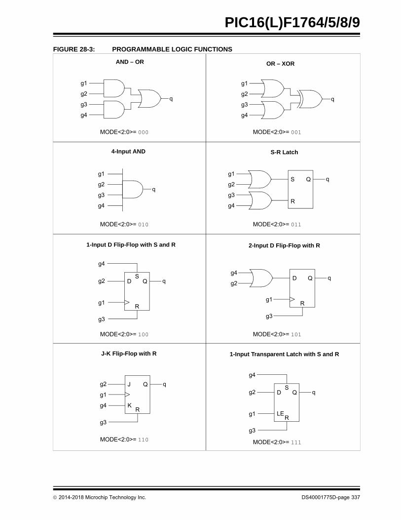
2014-2018 Microchip Technology Inc. DS40001775D-page 337
PIC16(L)F1764/5/8/9
FIGURE 28-3: PROGRAMMABLE LOGIC FUNCTIONS
g1
g2
g3
g4
q
g1
g2
g3
g4
q
g1
g2
g3
g4
q
S
R
Qg1
g2
g3
g4
q
D Q
g1
g2
g3
g4
qS
R
J Qg2
g3
g4
q
R
g1
K
D Q
g1
g2
g3
g4
qS
R
D Q
g1
g3
q
R
g4
g2
MODE<2:0>= 000
MODE<2:0>= 010
MODE<2:0>= 001
MODE<2:0>= 011
MODE<2:0>= 100
MODE<2:0>= 110
MODE<2:0>= 101
MODE<2:0>= 111
LE
AND – OR OR – XOR
4-Input AND S-R Latch
1-Input D Flip-Flop with S and R 2-Input D Flip-Flop with R
1-Input Transparent Latch with S and RJ-K Flip-Flop with R

2014-2018 Microchip Technology Inc. DS40001775D-page 338
PIC16(L)F1764/5/8/9
28.6 Register Definitions: CLC Control
Long bit name prefixes for the CLC peripherals areshown in Table 28-3. Refer to Section 1.1 “Registerand Bit Naming Conventions” for more information.
TABLE 28-3: BIT NAME PREFIXES
Peripheral Bit Name Prefix
CLC1 LC1
CLC2 LC2
REGISTER 28-1: CLCxCON: CLCx CONTROL REGISTER
R/W-0/0 U-0 R-0/0 R/W-0/0 R/W-0/0 R/W-0/0 R/W-0/0 R/W-0/0
EN — OUT INTP INTN MODE<2:0>
bit 7 bit 0
Legend:
R = Readable bit W = Writable bit
u = Bit is unchanged x = Bit is unknown U = Unimplemented bit, read as ‘0’
‘1’ = Bit is set ‘0’ = Bit is cleared -n/n = Value at POR and BOR/Value at all other Resets
bit 7 EN: CLCx Enable bit
1 = CLCx is enabled and mixing input signals0 = CLCx is disabled and has logic zero output
bit 6 Unimplemented: Read as ‘0’
bit 5 OUT: CLCx Data Output bit
Read-only: logic cell output data, after POL; sampled from lcx_out wire.
bit 4 INTP: CLCx Positive Edge Going Interrupt Enable bit
1 = CLCxIF will be set when a rising edge occurs on lcx_out0 = CLCxIF will not be set
bit 3 INTN: CLCx Negative Edge Going Interrupt Enable bit
1 = CLCxIF will be set when a falling edge occurs on lcx_out0 = CLCxIF will not be set
bit 2-0 MODE<2:0>: CLCx Functional Mode bits
111 = Cell is 1-Input Transparent Latch with S and R110 = Cell is J-K Flip-Flop with R101 = Cell is 2-Input D Flip-Flop with R100 = Cell is 1-Input D Flip-Flop with S and R011 = Cell is S-R Latch010 = Cell is 4-Input AND001 = Cell is OR-XOR000 = Cell is AND-OR

2014-2018 Microchip Technology Inc. DS40001775D-page 339
PIC16(L)F1764/5/8/9
REGISTER 28-2: CLCxPOL: CLCx SIGNAL POLARITY CONTROL REGISTER
R/W-0/0 U-0 U-0 U-0 R/W-x/u R/W-x/u R/W-x/u R/W-x/u
POL — — — G4POL G3POL G2POL G1POL
bit 7 bit 0
Legend:
R = Readable bit W = Writable bit
u = Bit is unchanged x = Bit is unknown U = Unimplemented bit, read as ‘0’
‘1’ = Bit is set ‘0’ = Bit is cleared -n/n = Value at POR and BOR/Value at all other Resets
bit 7 POL: LCOUT Polarity Control bit
1 = The output of the logic cell is inverted0 = The output of the logic cell is not inverted
bit 6-4 Unimplemented: Read as ‘0’
bit 3 G4POL: Gate 4 Output Polarity Control bit
1 = The output of Gate 4 is inverted when applied to the logic cell0 = The output of Gate 4 is not inverted
bit 2 G3POL: Gate 3 Output Polarity Control bit
1 = The output of Gate 3 is inverted when applied to the logic cell0 = The output of Gate 3 is not inverted
bit 1 G2POL: Gate 2 Output Polarity Control bit
1 = The output of Gate 2 is inverted when applied to the logic cell0 = The output of Gate 2 is not inverted
bit 0 G1POL: Gate 1 Output Polarity Control bit
1 = The output of Gate 1 is inverted when applied to the logic cell0 = The output of Gate 1 is not inverted
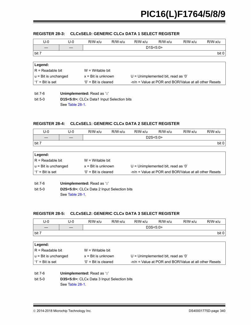
2014-2018 Microchip Technology Inc. DS40001775D-page 340
PIC16(L)F1764/5/8/9
REGISTER 28-3: CLCxSEL0: GENERIC CLCx DATA 1 SELECT REGISTER
U-0 U-0 R/W-x/u R/W-x/u R/W-x/u R/W-x/u R/W-x/u R/W-x/u
— — D1S<5:0>
bit 7 bit 0
Legend:
R = Readable bit W = Writable bit
u = Bit is unchanged x = Bit is unknown U = Unimplemented bit, read as ‘0’
‘1’ = Bit is set ‘0’ = Bit is cleared -n/n = Value at POR and BOR/Value at all other Resets
bit 7-6 Unimplemented: Read as ‘0’
bit 5-0 D1S<5:0>: CLCx Data1 Input Selection bits
See Table 28-1.
REGISTER 28-4: CLCxSEL1: GENERIC CLCx DATA 2 SELECT REGISTER
U-0 U-0 R/W-x/u R/W-x/u R/W-x/u R/W-x/u R/W-x/u R/W-x/u
— — D2S<5:0>
bit 7 bit 0
Legend:
R = Readable bit W = Writable bit
u = Bit is unchanged x = Bit is unknown U = Unimplemented bit, read as ‘0’
‘1’ = Bit is set ‘0’ = Bit is cleared -n/n = Value at POR and BOR/Value at all other Resets
bit 7-6 Unimplemented: Read as ‘0’
bit 5-0 D2S<5:0>: CLCx Data 2 Input Selection bits
See Table 28-1.
REGISTER 28-5: CLCxSEL2: GENERIC CLCx DATA 3 SELECT REGISTER
U-0 U-0 R/W-x/u R/W-x/u R/W-x/u R/W-x/u R/W-x/u R/W-x/u
— — D3S<5:0>
bit 7 bit 0
Legend:
R = Readable bit W = Writable bit
u = Bit is unchanged x = Bit is unknown U = Unimplemented bit, read as ‘0’
‘1’ = Bit is set ‘0’ = Bit is cleared -n/n = Value at POR and BOR/Value at all other Resets
bit 7-6 Unimplemented: Read as ‘0’
bit 5-0 D3S<5:0>: CLCx Data 3 Input Selection bits
See Table 28-1.

2014-2018 Microchip Technology Inc. DS40001775D-page 341
PIC16(L)F1764/5/8/9
REGISTER 28-6: CLCxSEL3: GENERIC CLCx DATA 4 SELECT REGISTER
U-0 U-0 R/W-x/u R/W-x/u R/W-x/u R/W-x/u R/W-x/u R/W-x/u
— — D4S<5:0>
bit 7 bit 0
Legend:
R = Readable bit W = Writable bit
u = Bit is unchanged x = Bit is unknown U = Unimplemented bit, read as ‘0’
‘1’ = Bit is set ‘0’ = Bit is cleared -n/n = Value at POR and BOR/Value at all other Resets
bit 7-6 Unimplemented: Read as ‘0’
bit 5-0 D4S<5:0>: CLCx Data 4 Input Selection bits
See Table 28-1.
REGISTER 28-7: CLCxGLS0: CLCx GATE 1 LOGIC SELECT REGISTER
R/W-x/u R/W-x/u R/W-x/u R/W-x/u R/W-x/u R/W-x/u R/W-x/u R/W-x/u
G1D4T G1D4N G1D3T G1D3N G1D2T G1D2N G1D1T G1D1N
bit 7 bit 0
Legend:
R = Readable bit W = Writable bit
u = Bit is unchanged x = Bit is unknown U = Unimplemented bit, read as ‘0’
‘1’ = Bit is set ‘0’ = Bit is cleared -n/n = Value at POR and BOR/Value at all other Resets
bit 7 G1D4T: Gate 1 Data 4 True (non-inverted) bit
1 = d4T is gated into g10 = d4T is not gated into g1
bit 6 G1D4N: Gate 1 Data 4 Negated (inverted) bit
1 = d4N is gated into g10 = d4N is not gated into g1
bit 5 G1D3T: Gate 1 Data 3 True (non-inverted) bit
1 = d3T is gated into g10 = d3T is not gated into g1
bit 4 G1D3N: Gate 1 Data 3 Negated (inverted) bit
1 = d3N is gated into g10 = d3N is not gated into g1
bit 3 G1D2T: Gate 1 Data 2 True (non-inverted) bit
1 = d2T is gated into g10 = d2T is not gated into g1
bit 2 G1D2N: Gate 1 Data 2 Negated (inverted) bit
1 = d2N is gated into g10 = d2N is not gated into g1
bit 1 G1D1T: Gate 1 Data 1 True (non-inverted) bit
1 = d1T is gated into g10 = d1T is not gated into g1
bit 0 G1D1N: Gate 1 Data 1 Negated (inverted) bit
1 = d1N is gated into g10 = d1N is not gated into g1

2014-2018 Microchip Technology Inc. DS40001775D-page 342
PIC16(L)F1764/5/8/9
REGISTER 28-8: CLCxGLS1: CLCx GATE 2 LOGIC SELECT REGISTER
R/W-x/u R/W-x/u R/W-x/u R/W-x/u R/W-x/u R/W-x/u R/W-x/u R/W-x/u
G2D4T G2D4N G2D3T G2D3N G2D2T G2D2N G2D1T G2D1N
bit 7 bit 0
Legend:
R = Readable bit W = Writable bit
u = Bit is unchanged x = Bit is unknown U = Unimplemented bit, read as ‘0’
‘1’ = Bit is set ‘0’ = Bit is cleared -n/n = Value at POR and BOR/Value at all other Resets
bit 7 G2D4T: Gate 2 Data 4 True (non-inverted) bit
1 = d4T is gated into g20 = d4T is not gated into g2
bit 6 G2D4N: Gate 2 Data 4 Negated (inverted) bit
1 = d4N is gated into g20 = d4N is not gated into g2
bit 5 G2D3T: Gate 2 Data 3 True (non-inverted) bit
1 = d3T is gated into g20 = d3T is not gated into g2
bit 4 G2D3N: Gate 2 Data 3 Negated (inverted) bit
1 = d3N is gated into g20 = d3N is not gated into g2
bit 3 G2D2T: Gate 2 Data 2 True (non-inverted) bit
1 = d2T is gated into g20 = d2T is not gated into g2
bit 2 G2D2N: Gate 2 Data 2 Negated (inverted) bit
1 = d2N is gated into g20 = d2N is not gated into g2
bit 1 G2D1T: Gate 2 Data 1 True (non-inverted) bit
1 = d1T is gated into g20 = d1T is not gated into g2
bit 0 G2D1N: Gate 2 Data 1 Negated (inverted) bit
1 = d1N is gated into g20 = d1N is not gated into g2

2014-2018 Microchip Technology Inc. DS40001775D-page 343
PIC16(L)F1764/5/8/9
REGISTER 28-9: CLCxGLS2: CLCx GATE 3 LOGIC SELECT REGISTER
R/W-x/u R/W-x/u R/W-x/u R/W-x/u R/W-x/u R/W-x/u R/W-x/u R/W-x/u
G3D4T G3D4N G3D3T G3D3N G3D2T G3D2N G3D1T G3D1N
bit 7 bit 0
Legend:
R = Readable bit W = Writable bit
u = Bit is unchanged x = Bit is unknown U = Unimplemented bit, read as ‘0’
‘1’ = Bit is set ‘0’ = Bit is cleared -n/n = Value at POR and BOR/Value at all other Resets
bit 7 G3D4T: Gate 3 Data 4 True (non-inverted) bit
1 = d4T is gated into g30 = d4T is not gated into g3
bit 6 G3D4N: Gate 3 Data 4 Negated (inverted) bit
1 = d4N is gated into g30 = d4N is not gated into g3
bit 5 G3D3T: Gate 3 Data 3 True (non-inverted) bit
1 = d3T is gated into g30 = d3T is not gated into g3
bit 4 G3D3N: Gate 3 Data 3 Negated (inverted) bit
1 = d3N is gated into g30 = d3N is not gated into g3
bit 3 G3D2T: Gate 3 Data 2 True (non-inverted) bit
1 = d2T is gated into g30 = d2T is not gated into g3
bit 2 G3D2N: Gate 3 Data 2 Negated (inverted) bit
1 = d2N is gated into g30 = d2N is not gated into g3
bit 1 G3D1T: Gate 3 Data 1 True (non-inverted) bit
1 = d1T is gated into g30 = d1T is not gated into g3
bit 0 G3D1N: Gate 3 Data 1 Negated (inverted) bit
1 = d1N is gated into g30 = d1N is not gated into g3

2014-2018 Microchip Technology Inc. DS40001775D-page 344
PIC16(L)F1764/5/8/9
REGISTER 28-10: CLCxGLS3: CLCx GATE 4 LOGIC SELECT REGISTER
R/W-x/u R/W-x/u R/W-x/u R/W-x/u R/W-x/u R/W-x/u R/W-x/u R/W-x/u
G4D4T G4D4N G4D3T G4D3N G4D2T G4D2N G4D1T G4D1N
bit 7 bit 0
Legend:
R = Readable bit W = Writable bit
u = Bit is unchanged x = Bit is unknown U = Unimplemented bit, read as ‘0’
‘1’ = Bit is set ‘0’ = Bit is cleared -n/n = Value at POR and BOR/Value at all other Resets
bit 7 G4D4T: Gate 4 Data 4 True (non-inverted) bit
1 = d4T is gated into g40 = d4T is not gated into g4
bit 6 G4D4N: Gate 4 Data 4 Negated (inverted) bit
1 = d4N is gated into g40 = d4N is not gated into g4
bit 5 G4D3T: Gate 4 Data 3 True (non-inverted) bit
1 = d3T is gated into g40 = d3T is not gated into g4
bit 4 G4D3N: Gate 4 Data 3 Negated (inverted) bit
1 = d3N is gated into g40 = d3N is not gated into g4
bit 3 G4D2T: Gate 4 Data 2 True (non-inverted) bit
1 = d2T is gated into g40 = d2T is not gated into g4
bit 2 G4D2N: Gate 4 Data 2 Negated (inverted) bit
1 = d2N is gated into g40 = d2N is not gated into g4
bit 1 G4D1T: Gate 4 Data 1 True (non-inverted) bit
1 = d1T is gated into g40 = d1T is not gated into g4
bit 0 G4D1N: Gate 4 Data 1 Negated (inverted) bit
1 = d1N is gated into g40 = d1N is not gated into g4

2014-2018 Microchip Technology Inc. DS40001775D-page 345
PIC16(L)F1764/5/8/9
REGISTER 28-11: CLCxDATA: CLCx DATA OUTPUT
U-0 U-0 U-0 U-0 U-0 R-0 R-0 R-0
— — — — — MLC3OUT MLC2OUT MLC1OUT
bit 7 bit 0
Legend:
R = Readable bit W = Writable bit
u = Bit is unchanged x = Bit is unknown U = Unimplemented bit, read as ‘0’
‘1’ = Bit is set ‘0’ = Bit is cleared -n/n = Value at POR and BOR/Value at all other Resets
bit 7-3 Unimplemented: Read as ‘0’
bit 2 MLC3OUT: Mirror copy of LC3OUT bit
bit 1 MLC2OUT: Mirror copy of LC2OUT bit
bit 0 MLC1OUT: Mirror copy of LC1OUT bit
TABLE 28-4: SUMMARY OF REGISTERS ASSOCIATED WITH CLCx
Name Bit7 Bit6 Bit5 Bit4 BIt3 Bit2 Bit1 Bit0Register on Page
ANSELA — — — ANSA4 — ANSA<2:0> 137
ANSELB(1) ANSB<7:4> — — — — 143
ANSELC ANSC<7:6>(1) — — ANSC<3:0> 148
CLCxCON EN — OUT INTP INTN MODE<2:0> 338
CLCDATA — — — — — MLC3OUT MLC2OUT MLC1OUT 345
CLCxGLS0 G1D4T G1D4N G1D3T G1D3N G1D2T G1D2N G1D1T G1D1N 341
CLCxGLS1 G2D4T G2D4N G2D3T G2D3N G2D2T G2D2N G2D1T G2D1N 342
CLCxGLS2 G3D4T G3D4N G3D3T G3D3N G3D2T G3D2N G3D1T G3D1N 343
CLCxGLS3 G4D4T G4D4N G4D3T G4D3N G4D2T G4D2N G4D1T G4D1N 344
CLCxPOL POL — — — G4POL G3POL G2POL G1POL 339
CLCxSEL0 — — D1S<5:0> 340
CLCxSEL1 — — D2S<5:0> 340
CLCxSEL2 — — D3S<5:0> 340
CLCxSEL3 — — D4S<5:0> 341
CLCxPPS — — — CLCxPPS<4:0> 154, 156
INTCON GIE PEIE TMR0IE INTE IOCIE TMR0IF INTF IOCIF 101
PIE3 PWM6IE(1) PWM5IE COG1IE ZCDIE COG2IE(1) CLC3IE CLC2IE CLC1IE 104
PIR3 PWM6IF(1) PWM5IF COG1IF ZCDIF COG2IF(1) CLC3IF CLC2IF CLC1IF 107
RxyPPS — — — RxyPPS<4:0> 154
TRISA — — TRISA<5:4> —(3) TRISA<2:0> 136
TRISB(1) TRISB<7:4> — — — — 142
TRISC TRISC<7:6>(1) TRISC<5:0> 147
Legend: — = unimplemented location, read as ‘0’. Shaded cells are not used for CLCx module.
Note 1: PIC16(L)F1768/9 only.
2: Unimplemented, read as ‘1’.

2014-2018 Microchip Technology Inc. DS40001775D-page 346
PIC16(L)F1764/5/8/9
29.0 OPERATIONAL AMPLIFIER (OPA) MODULES
The Operational Amplifier (OPA) is a standard three-terminal device requiring external feedback to operate.The OPA module has the following features:
• External connections to I/O ports
• Low leakage inputs
• Factory calibrated input offset voltage
• Unity gain control
• Programmable positive and negative source selections
• Override controls:
- Forced tri-state output
- Forced unity gain
FIGURE 29-1: OPAx MODULE BLOCK DIAGRAM
OPA
EN
PCH<1:0>
OPAXOUT
OPAxIN0+
0
1
UG
NCH<1:0>
OPAxIN1+
OPAxIN0-
OPAxIN1-
OPAx_out
ORS<1:0>
ORM1
ORM0
Internal Override Sources, See Register 29-2.
Internal Analog Sources, See Register 29-4.
Internal Analog Sources, See Register 29-3.
ORPOL

2014-2018 Microchip Technology Inc. DS40001775D-page 347
PIC16(L)F1764/5/8/9
29.1 OPA Module Performance
Common AC and DC performance specifications forthe OPA module:
• Common-Mode Voltage Range
• Leakage Current
• Input Offset Voltage
• Open-Loop Gain
• Gain Bandwidth Product
Common-mode voltage range is the specifiedvoltage range for the OPA+ and OPA- inputs, for whichthe OPA module will perform to within its specifications.The OPA module is designed to operate with inputvoltages between VSS and VDD. Behavior for Common-mode voltages greater than VDD, or below VSS, are notguaranteed.
Leakage current is a measure of the small source orsink currents on the OPA+ and OPA- inputs. Tominimize the effect of leakage currents, the effectiveimpedances connected to the OPA+ and OPA- inputsshould be kept as small as possible and equal.
Input offset voltage is a measure of the voltagedifference between the OPA+ and OPA- inputs in aclosed loop circuit with the OPA in its linear region. Theoffset voltage will appear as a DC offset in the outputequal to the input offset voltage, multiplied by the gain ofthe circuit. The input offset voltage is also affected by theCommon-mode voltage. The OPA is factory calibrated tominimize the input offset voltage of the module.
Open-loop gain is the ratio of the output voltage to thedifferential input voltage, (OPA+) – (OPA-). The gain isgreatest at DC and falls off with frequency.
Gain Bandwidth Product or GBWP is the frequencyat which the open-loop gain falls off to 0 dB.
29.2 OPA Module Control
The OPA module is enabled by setting the OPAxEN bitof the OPAxCON register (Register 29-1). Whenenabled, the OPA forces the output driver of OPAxOUTpin into tri-state to prevent contention between thedriver and the OPA output.
29.2.1 UNITY GAIN MODE
The OPAxUG bit of the OPAxCON register(Register 29-1) selects the Unity Gain mode. Whenunity gain is selected, the OPA output is connected tothe inverting input and the OPAxIN pin is relinquished,releasing the pin for general purpose input and output.
29.2.2 PROGRAMMABLE SOURCE SELECTIONS
The inverting and non-inverting sources are selectedwith the OPAxNCHS (Register 29-3) and OPAxPCHS(Register 29-4) registers, respectively. Sources include:
• Internal DACs
• Device pins
• Internal slope compensation ramp generator
• Other op amps in the device
29.3 Override Control
29.3.1 OVERRIDE MODE
The op amp operation can be overridden in two ways:
• Forced tri-state output
• Force unity gain
The Override mode is selected with the ORM<1:0> bitsof the OPxCON register (Register 29-1). The overrideis in effect when the mode is selected and the overridesource is true.
29.3.2 OVERRIDE SOURCES
The override source is selected with the OPAxORSregister (Register 29-2). Sources are from internalperipherals including:
• CCP outputs
• PWM outputs
• Comparator outputs
• Zero-Cross Detect (ZCD) output
• Configurable Logic Cell outputs
• COG outputs
29.3.3 OVERRIDE SOURCE POLARITY
The override source polarity can be inverted so that theoverride will occur on either the high or low level of theselected source. Override polarity is controlled by theORPOL bit of the OPAxCON register (Register 29-1).
29.4 Effects of Reset
A device Reset forces all registers to their Reset state.This disables the OPA module.
29.5 Effects of Sleep
The operational amplifier continues to operate whenthe device is put in Sleep mode.
Note: When the OPA module is enabled, theOPAxOUT pin is driven by the op ampoutput, not by the PORT digital driver.Refer to Table 36-17: Operational Amplifier(OPA) for the op amp output drivecapability.

2014-2018 Microchip Technology Inc. DS40001775D-page 348
PIC16(L)F1764/5/8/9
29.6 Register Definitions: Op Amp Control
Long bit name prefixes for the op amp peripherals areshown in Table 29-1. Refer to Section 1.1 “Registerand Bit Naming Conventions” for more information.
TABLE 29-1: BIT NAME PREFIXES
Peripheral Bit Name Prefix
OPA1 OPA1
OPA2(1) OPA2
Note 1: PIC16(L)F1768/9 devices only.
REGISTER 29-1: OPAxCON: OPERATIONAL AMPLIFIER x (OPAx) CONTROL REGISTER
R/W-0/0 U-0 U-0 R/W-0/0 U-0 R/W-0/0 R/W-0/0 R/W-0/0
EN — — UG — ORPOL ORM<1:0>
bit 7 bit 0
Legend:
R = Readable bit W = Writable bit
u = Bit is unchanged x = Bit is unknown U = Unimplemented bit, read as ‘0’
‘1’ = Bit is set ‘0’ = Bit is cleared -n/n = Value at POR and BOR/Value at all other Resets
bit 7 EN: Op Amp Enable bit
1 = Op amp is enabled0 = Op amp is disabled and consumes no active power
bit 6-5 Unimplemented: Read as ‘0’
bit 4 UG: Op Amp Unity Gain Select bit
1 = OPA output is connected to inverting input; OPAxIN- pin is available for general purpose I/O0 = Inverting input is connected to the OPAxIN- pin
bit 3 Unimplemented: Read as ‘0’
bit 2 ORPOL: Op Amp Override Source Polarity bit
1 = Override source polarity is inverted; override occurs when source is high0 = Override source polarity is not inverted; override occurs when source is low
bit 1-0 ORM<1:0>: Op Amp Override Mode Selection bits
11 = Reserved; do not use10 = Op amp is forced to unity gain when override source is true01 = Op amp output is tri-stated when override source is true00 = Output override function is disabled
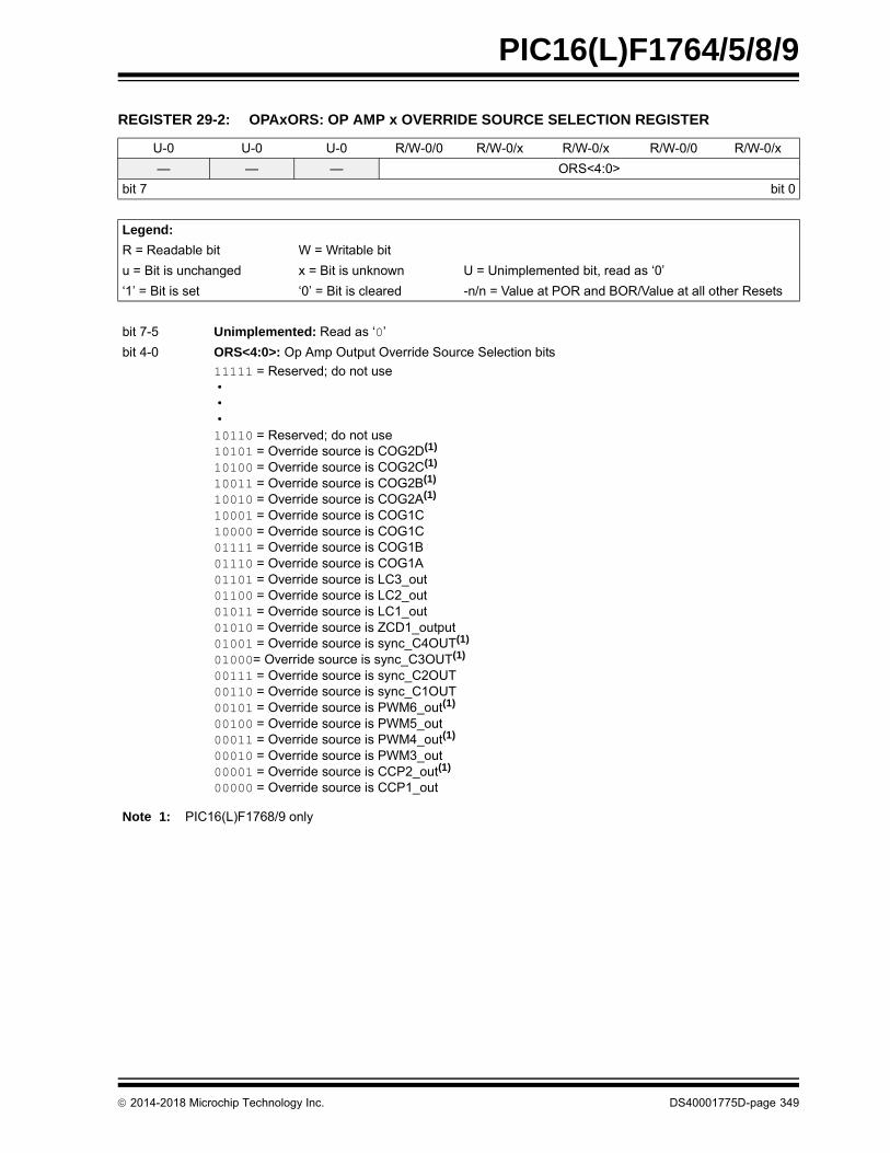
2014-2018 Microchip Technology Inc. DS40001775D-page 349
PIC16(L)F1764/5/8/9
REGISTER 29-2: OPAxORS: OP AMP x OVERRIDE SOURCE SELECTION REGISTER
U-0 U-0 U-0 R/W-0/0 R/W-0/x R/W-0/x R/W-0/0 R/W-0/x
— — — ORS<4:0>
bit 7 bit 0
Legend:
R = Readable bit W = Writable bit
u = Bit is unchanged x = Bit is unknown U = Unimplemented bit, read as ‘0’
‘1’ = Bit is set ‘0’ = Bit is cleared -n/n = Value at POR and BOR/Value at all other Resets
bit 7-5 Unimplemented: Read as ‘0’
bit 4-0 ORS<4:0>: Op Amp Output Override Source Selection bits
11111 = Reserved; do not use • • •10110 = Reserved; do not use10101 = Override source is COG2D(1)
10100 = Override source is COG2C(1)
10011 = Override source is COG2B(1)
10010 = Override source is COG2A(1)
10001 = Override source is COG1C10000 = Override source is COG1C01111 = Override source is COG1B01110 = Override source is COG1A01101 = Override source is LC3_out01100 = Override source is LC2_out01011 = Override source is LC1_out01010 = Override source is ZCD1_output01001 = Override source is sync_C4OUT(1)
01000= Override source is sync_C3OUT(1)
00111 = Override source is sync_C2OUT00110 = Override source is sync_C1OUT00101 = Override source is PWM6_out(1)
00100 = Override source is PWM5_out00011 = Override source is PWM4_out(1)
00010 = Override source is PWM3_out00001 = Override source is CCP2_out(1)
00000 = Override source is CCP1_out
Note 1: PIC16(L)F1768/9 only

2014-2018 Microchip Technology Inc. DS40001775D-page 350
PIC16(L)F1764/5/8/9
REGISTER 29-3: OPAxNCHS: OP AMP x NEGATIVE CHANNEL SOURCE SELECT REGISTER
U-0 U-0 U-0 U-0 R/W-0/0 R/W-0/0 R/W-0/0 R/W-0/0
— — — — NCH<3:0>
bit 7 bit 0
Legend:
R = Readable bit W = Writable bit
u = Bit is unchanged x = Bit is unknown U = Unimplemented bit, read as ‘0’
‘1’ = Bit is set ‘0’ = Bit is cleared -n/n = Value at POR and BOR/Value at all other Resets
bit 7-4 Unimplemented: Read as ‘0’
bit 3-0 NCH<3:0>: Op Amp Inverting Input Channel Selection bits
1111 = Reserved; do not use • • •1010 = Reserved; do not use1001 = Programmable Ramp Generator PRG2_out(1)
1000 = Programmable Ramp Generator PRG1_out0111 = Reserved. Do not use.0110 = FVR_Buffer20101 = DAC4_out(1)
0100 = DAC3_out0011 = DAC2_out(1)
0010 = DAC1_out0001 = OPAxIN1- pin(1)
0000 = OPAxIN0- pin
Note 1: PIC16(L)F1768/9 only

2014-2018 Microchip Technology Inc. DS40001775D-page 351
PIC16(L)F1764/5/8/9
TABLE 29-2: SUMMARY OF REGISTERS ASSOCIATED WITH OP AMPS
REGISTER 29-4: OPAxPCHS: OP AMP x POSITIVE CHANNEL SOURCE SELECT REGISTER
U-0 U-0 U-0 U-0 R/W-0/0 R/W-0/0 R/W-0/0 R/W-0/0
— — — — PCH<3:0>
bit 7 bit 0
Legend:
R = Readable bit W = Writable bit
u = Bit is unchanged x = Bit is unknown U = Unimplemented bit, read as ‘0’
‘1’ = Bit is set ‘0’ = Bit is cleared -n/n = Value at POR and BOR/Value at all other Resets
bit 7-4 Unimplemented: Read as ‘0’
bit 3-0 PCH<3:0>: Op Amp Non-Inverting Input Channel Selection bits
1111 = Reserved; do not use • • •1010 = Reserved; do not use1001 = Programmable Ramp Generator PRG2_out(1)
1000 = Programmable Ramp Generator PRG1_out0111 = Reserved. Do not use.0110 = FVR_Buffer20101 = DAC4_out(1)
0100 = DAC3_out0011 = DAC2_out(1)
0010 = DAC1_out0001 = OPAxIN1+ pin(1)
0000 = OPAxIN0+ pin
Note 1: PIC16(L)F1768/9 only
Name Bit 7 Bit 6 Bit 5 Bit 4 Bit 3 Bit 2 Bit 1 Bit 0Register on Page
ANSELB(2) ANSB<7:6> ANSB<5:4> — — — — 143
ANSELC(2) ANSC<7:6>(2) — — ANSC<3:2> ANSC<1:0> 148
DACxCON0 EN FM OE1 — PSS<1:0> NSS<1:0> 188
DACxREF --- --- --- REF<4:0> 189
DACxREFL(2) REF<7:0> 194
DACxREFH(2) REF<15:8> 194
FVRCON FVREN FVRRDY TSEN TSRNG CDAFVR<1:0> ADFVR<1:0> 169
OPAxCON EN — — UG — ORPOL ORM<1:0> 348
OPAxNCHS — — — — NCH<3:0> 350
OPAxPCHS — — — — PCH<3:0> 351
OPAxORS — — — ORS<4:0> 349
TRISB(2) TRISB<7:6> TRISB<5:4> — — — — 142
TRISC(2) TRISC<7:6>(2) TRISC<5:4> TRISC<3:2> TRISC<1:0> 147
Legend: — = unimplemented location, read as ‘0’. Shaded cells are not used by op amps.Note 1: Unimplemented, read as ‘1’.
2: PIC16(L)F1768/9 only

2014-2018 Microchip Technology Inc. DS40001775D-page 352
PIC16(L)F1764/5/8/9
30.0 PROGRAMMABLE RAMP GENERATOR (PRG) MODULE
The Programmable Ramp Generator (PRG) module isdesigned to provide rising and falling linear ramps.Typical applications include slope compensation forfixed frequency, continuous current and Current modeswitched power supplies. Slope compensation is anecessary feature of these power supplies because itprevents frequency instabilities at duty cycles greaterthan 50%.
The PRG has the following features:
• Linear positive and negative voltage ramp outputs
• Programmable current source/sink
• Internal and external reference voltage selection
• Internal and external timing source selection
A simplified block diagram of the PRG is shown inFigure 30-1.
30.1 Fundamental Operation
The PRG can be operated in three voltage rampgenerator modes:
• Falling Voltage (slope compensation)
• Rising Voltage
• Alternating Rising and Falling Voltage
In the Rising or Falling mode, an internal capacitor isdischarged when the set_falling timing input is true andcharged by an internally generated constant currentwhen the set_rising timing input is true. The resultinglinear ramp starts at the selected voltage input leveland resets back to that level when the ramp is termi-nated by the set_falling timing input. The set_fallinginput dominates when both timing inputs are true.
To control the operation with a single-ended source,select the same source for both the set_rising andset_falling inputs and invert the polarity of one of themwith the corresponding polarity control bit.
In the Alternating mode, the capacitor is not dischargedbut alternates between being charged in one directionthen the other.
Input selections are identical for all modes. The inputvoltage is supplied by any of the following:
• The PRGxIN0 or PRGxIN1 pins
• The buffered output of the internal Fixed Voltage Reference (FVR),
• Any of the internal DACs.
The timing sources are selected from the following:
• The synchronized output of any comparator
• Any PWM output
• Any I/O pin
The ramp output is available as an input to any of thecomparators or op amps.
30.1.1 SLOPE COMPENSATION
Slope compensation works by quickly discharging aninternal capacitor at the beginning of each PWM period.One side of the internal capacitor is connected to thevoltage input source and the other side is connected tothe internal current sink. The internal current sinkcharges this capacitor at a programmable rate. As thecapacitor charges, the capacitor voltage is subtractedfrom the voltage source, producing a linear voltagedecay at the required rate (see Figure 30-2). The rampterminates and the capacitor is discharged when theset_falling timing input goes true. The next ramp startswhen the set_rising timing input goes true.
Enabling the optional one-shot by setting the OS bit ofthe PRGxCON0 register ensures that the capacitor isfully discharged by overriding the set_rising timing inputand holding the shorting switch closed for at least theone-shot period, typically 50 ns. Edge-sensitive timinginputs that occur during the one-shot period will beignored. Level-sensitive timing inputs that occur during,and extend beyond, the one-shot period will besuspended until the end of the one-shot time.
30.1.2 RAMP GENERATION
Ramp generation is similar to slope compensationexcept that the slope is either both rising and falling orjust rising.
30.1.2.1 Alternating Rising/Falling Ramps
The alternating rising/falling ramp generation functionworks by employing the built-in current source and sink,and relying on the synchronous control of the internalanalog switches and timing sources to ramp the module’soutput voltage up, and then subsequently, down.
Once initialized, the output voltage is ramped up linearlyby the current source at a programmable rate until theset_falling timing source goes true, at which point thecurrent source is disengaged. At the same time, thecurrent sink is engaged to linearly ramp down the outputvoltage, also at a programmable rate, until the set_risingtiming input goes true thereby reversing the ramp slope.The process then repeats to create a saw tooth likewaveform, as shown in Figure 30-3 and Figure 30-4.
The set_rising and set_falling timing inputs can beeither edge or level-sensitive, which is selected with therespective REDG and FEDG bits of the PRGxCON0register. Edge-sensitive operation is recommended forperiodic signals, such as clocks, and level-sensitiveoperation is recommended for analog limit triggers,such as comparator outputs.
When the one-shot is enabled (OS bit is set), then boththe falling and rising ramps will persist for a minimum ofthe one-shot period. Edge-sensitive timing inputs thatoccur during the one-shot period will be ignored.Level-sensitive timing inputs that occur during, andextend beyond, the one-shot period will be suspendeduntil the end of the one-shot time.
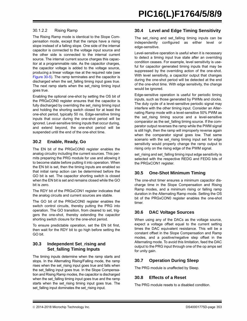
2014-2018 Microchip Technology Inc. DS40001775D-page 353
PIC16(L)F1764/5/8/9
30.1.2.2 Rising Ramp
The Rising Ramp mode is identical to the Slope Com-pensation mode, except that the ramps have a risingslope instead of a falling slope. One side of the internalcapacitor is connected to the voltage input source andthe other side is connected to the internal currentsource. The internal current source charges this capac-itor at a programmable rate. As the capacitor charges,the capacitor voltage is added to the voltage source,producing a linear voltage rise at the required rate (seeFigure 30-5). The ramp terminates and the capacitor isdischarged when the set_falling timing input goes true.The next ramp starts when the set_rising timing inputgoes true.
Enabling the optional one-shot by setting the OS bit ofthe PRGxCON0 register ensures that the capacitor isfully discharged by overriding the set_rising timing inputand holding the shorting switch closed for at least theone-shot period, typically 50 ns. Edge-sensitive timinginputs that occur during the one-shot period will beignored. Level-sensitive timing inputs that occur during,and extend beyond, the one-shot period will besuspended until the end of the one-shot time.
30.2 Enable, Ready, Go
The EN bit of the PRGxCON0 register enables theanalog circuitry including the current sources. This per-mits preparing the PRG module for use and allowing itto become stable before putting it into operation. Whenthe EN bit is set, then the timing inputs are enabled sothat initial ramp action can be determined before theGO bit is set. The capacitor shorting switch is closedwhen the EN bit is set and remains closed while the GObit is zero.
The RDY bit of the PRGxCON1 register indicates thatthe analog circuits and current sources are stable.
The GO bit of the PRGxCON0 register enables theswitch control circuits, thereby putting the PRG intooperation. The GO transition, from cleared to set, trig-gers the one-shot, thereby extending the capacitorshorting switch closure for the one-shot period.
To ensure predictable operation, set the EN bit first,then wait for the RDY bit to go high before setting theGO bit.
30.3 Independent Set_rising and Set_falling Timing Inputs
The timing inputs determine when the ramp starts andstops. In the Alternating Rising/Falling mode, the ramprises when the set_rising input goes true and falls whenthe set_falling input goes true. In the Slope Compensa-tion and Rising Ramp modes, the capacitor is dischargedwhen the set_falling timing input goes true and the rampstarts when the set_rising timing input goes true. Theset_falling input dominates the set_rising input.
30.4 Level and Edge Timing Sensitivity
The set_rising and set_falling timing inputs can beindependently configured as either level oredge-sensitive.
Level-sensitive operation is useful when it is necessaryto detect a timing input true state after an overridingcondition ceases. For example, level sensitivity is use-ful for capacitor generated timing inputs that may besuppressed by the overriding action of the one-shot.With level sensitivity, a capacitor output that changesduring the one-shot period will be detected at the endof the one-shot time. With edge sensitivity, the changewould be ignored.
Edge-sensitive operation is useful for periodic timinginputs, such as those generated by PWMs and clocks.The duty cycle of a level-sensitive periodic signal mayinterfere with the other timing input. Consider an Alter-nating Ramp mode with a level-sensitive 50% PWM asthe set_rising timing source and a level-sensitivecomparator as the set_falling timing source. If the com-parator output reverses the ramp while the PWM signalis still high, then the ramp will improperly reverse againwhen the comparator signal goes low. That samescenario with the set_rising timing input set for edgesensitivity would properly change the ramp output torising only on the rising edge of the PWM signal.
set_rising and set_falling timing input edge sensitivity isselected with the respective REDG and FEDG bits ofthe PRGxCON1 register.
30.5 One-Shot Minimum Timing
The one-shot timer ensures a minimum capacitor dis-charge time in the Slope Compensation and RisingRamp modes, and a minimum rising or falling rampduration in the Alternating Ramp mode. Setting the OSbit of the PRGxCON0 register enables the one-shottimer.
30.6 DAC Voltage Sources
When using any of the DACs as the voltage source,expect a voltage offset equal to the current settingtimes the DAC equivalent resistance. This will be aconstant offset in the Slope Compensation and Rampmodes, and a positive/negative step offset in theAlternating mode. To avoid this limitation, feed the DACoutput to the PRG input through one of the op amps setfor unity gain.
30.7 Operation During Sleep
The PRG module is unaffected by Sleep.
30.8 Effects of a Reset
The PRG module resets to a disabled condition.

2
01
4-2
01
8 M
icroch
ip T
ech
no
log
y Inc.
DS
40
00
17
75
D-p
ag
e 3
54
PIC
16(L)F
1764/5/8/9
FIGURE 30-1: SIMPLIFIED PRG MODULE BLOCK DIAGRAM
PRGxIN
RTSS<3:0>
FPOL
FTSS<3:0>
ISET<4:0>
RAMPx_out toperipherals
VDDRev. 10-000220B
12/21/2017
SW1
SW3
SW2RPOL
SwitchControl
REDG
FEDG
EN
ISET<4:0>
MODE<1:0>
INS<3:0>
PRGxR
PRGxF
GO
Voltage Sources
Set_rising Timing Sources
Set_falling Timing Sources
R
S Q
OS
voltage_ref
PPS
PPS
PRGxRPPS
PRGxFPPS
LR
LR

PIC
16(L)F
1764/5/8/9
DS
40
00
17
75
D-p
ag
e 3
55
2
01
4-2
01
8 M
icroch
ip T
ech
no
log
y Inc.
FIGURE 30-2: SLOPE COMPENSATION (FALLING RAMP) TIMING DIAGRAM (MODE<1:0> = 00)Rev. 10-000 223A
5/2/201 4
EN
RDY
GO
Init Running
set_falling
one_shot
sw1_closed
voltage_ref
RAMPx_out
sw2_closed
sw3_closed
Init Running
OS
set_rising

2
01
4-2
01
8 M
icroch
ip T
ech
no
log
y Inc.
DS
40
00
17
75
D-p
ag
e 3
56
PIC
16(L)F
1764/5/8/9
FIGURE 30-3: ALTERNATING RISING/FALLING RAMP GENERATION TIMING DIAGRAM (OS = 0, MODE<1:0> = 01) Rev. 10-000 222A
4/29/201 4
EN
RDY
GO
set_rising
Init Running
set_falling
one_shot
sw1_closed
voltage_ref
RAMPx_out
sw2_closed
sw3_closed
Init Running
REDG
FEDG

PIC
16(L)F
1764/5/8/9
DS
40
00
17
75
D-p
ag
e 3
57
2
01
4-2
01
8 M
icroch
ip T
ech
no
log
y Inc.
FIGURE 30-4: ALTERNATING RISING/FALLING RAMP GENERATION TIMING DIAGRAM (OS = 1, MODE<1:0> = 01) Notes: Rev. 10-000 226A
5/2/201 4
EN
RDY
GO
set_rising
Init Running
set_falling
one_shot
sw1_closed
voltage_ref
RAMPx_out
sw2_closed
sw3_closed
Init Running
REDG
FEDG

2
01
4-2
01
8 M
icroch
ip T
ech
no
log
y Inc.
DS
40
00
17
75
D-p
ag
e 3
58
PIC
16(L)F
1764/5/8/9
FIGURE 30-5: RISING RAMP GENERATION TIMING DIAGRAM (MODE<1:0> = 10)
Rev. 10-000 224A5/2/201 4
EN
RDY
GO
Init Running
set_rising
one_shot
sw1_closed
voltage_ref
RAMPx_out
sw2_closed
sw3_closed
Init Running
OS
set_falling

2014-2018 Microchip Technology Inc. DS40001775D-page 359
PIC16(L)F1764/5/8/9
30.9 Slope Compensation Application
An example slope compensation circuit is shown inFigure 30-6. The PRG input voltage is PRGxIN whichshares an I/O pin with the op amp output. The op ampoutput is designed to operate at the expected peakcurrent sense voltage, which we’ll call VREF. The PRGoutput voltage starts at VREF and should fall at a rateless than half the target circuit current sense voltagerate of rise. Therefore, the compensator slope,expressed as volts per µs, can be computed byEquation 30-1.
EQUATION 30-1: COMPENSATOR SLOPE
For example, when the circuit is using a 1 currentsense resistor and the peak current is 1A, then thepeak current expressed as a voltage is 1V. Therefore,for this example the op amp output should be designedto operate at 1V. If the power supply PWM frequency is1 MHz, then the period is 1 s. Therefore, the desiredslope is 0.5 V/s, which is computed as shown inEquation 30-2.
EQUATION 30-2: CALCULATION EXAMPLE
FIGURE 30-6: EXAMPLE SLOPE COMPENSATION CIRCUIT
Vs------
VREF
2-------------
PWM Period (s --------------------------------------------
VREF
2-------------
PWM Period (s --------------------------------------------
12---
1s--------- 0.5V s= =
Note: The setting for 0.5V/s is ISET<4:0> = 6,LR = 0.
COG
-
+
PRG
COGxOUTx
CxINx-
RGxIN
VIN
L1
D1
C1
R1
R2
R3-
+OPAxOUT
OPAxIN-
C3
DAC
R4
R5C2
Rev. 10-000 221A5/7/201 4

2014-2018 Microchip Technology Inc. DS40001775D-page 360
PIC16(L)F1764/5/8/9
30.10 Register Definitions: Programmable Ramp Generator
Long bit name prefixes for the PRG peripherals areshown in Table 30-1. Refer to Section 1.1 “Registerand Bit Naming Conventions” for more information.
TABLE 30-1: BIT NAME PREFIXES
Peripheral Bit Name Prefix
PRG1 RG1
PRG2(1) RG2
Note 1: PIC16(L)F1768/9 devices only.
REGISTER 30-1: PRGxCON0: PROGRAMMABLE RAMP GENERATOR x CONTROL 0 REGISTER
R/W-0/0 U-0 R/W-0/0 R/W-0/0 R/W-0/0 R/W-0/0 R/W-0/0 R/W-0/0
EN — FEDG REDG MODE<1:0> OS GO
bit 7 bit 0
Legend:
R = Readable bit W = Writable bit U = Unimplemented bit, read as ‘0’
u = Bit is unchanged x = Bit is unknown U = Unimplemented bit, read as ‘0’
‘1’ = Bit is set ‘0’ = Bit is cleared -n/n = Value at POR and BOR/Value at all other Resets
bit 7 EN: Programmable Ramp Generator Enable bit
1 = PRG module is enabled0 = PRG module is disabled
bit 6 Unimplemented: Read as ‘0’
bit 5 FEDG: set_falling Input Mode Select bit
1 = set_falling timing input is edge-sensitive0 = set_falling timing input is level-sensitive
bit 4 REDG: set_rising Input Mode Select bit
1 = set_rising timing input is edge-sensitive0 = set_rising timing input is level-sensitive
bit 3-2 MODE<1:0>: Programmable Ramp Generator Mode Selection bits
11 = Reserved10 = Rising Ramp Generator01 = Alternating Rising/Falling Ramp Generator00 = Slope Compensation
bit 1 OS: One-Shot Enable bit
1 = One-shot is enabled; minimum capacitor discharge is internally timed by one-shot0 = One-shot is disabled; capacitor is discharged when timing input is true
bit 0 GO: Ramp Generation Control Start bit
If EN = 0:This bit is forced to ‘0’.
If EN = 1:1 = Slope or ramp function is operating0 = Slope or ramp function is not operating; all current source switches are open and capacitor
discharge switch is closed

2014-2018 Microchip Technology Inc. DS40001775D-page 361
PIC16(L)F1764/5/8/9
REGISTER 30-2: PRGxCON1: PROGRAMMABLE RAMP GENERATOR x CONTROL 1 REGISTER
U-0 U-0 U-0 U-0 U-0 R-0 R/W-0/0 R/W-0/0
— — — — — RDY FPOL RPOL
bit 7 bit 0
Legend:
R = Readable bit W = Writable bit
u = Bit is unchanged x = Bit is unknown U = Unimplemented bit, read as ‘0’
‘1’ = Bit is set ‘0’ = Bit is cleared -n/n = Value at POR and BOR/Value at all other Resets
bit 7-3 Unimplemented: Read as ‘0’
bit 2 RDY: Slope Generator Ready Status bit
1 = PRG is ready0 = PRG is not ready
bit 1 FPOL: Fall Event Polarity Select bit
1 = set_falling timing input is active-low0 = set_falling timing input is active-high
bit 0 RPOL: Rise Event Polarity Select bit
1 = set_rising timing input is active-low0 = set_rising timing input is active-high
REGISTER 30-3: PRGxINS: PRGx VOLTAGE INPUT SELECT REGISTER
U-0 U-0 U-0 U-0 R/W-0/0 R/W-0/0 R/W-0/0 R/W-0/0
— — — — INS<3:0>
bit 7 bit 0
Legend:
R = Readable bit W = Writable bit
u = Bit is unchanged x = Bit is unknown U = Unimplemented bit, read as ‘0’
‘1’ = Bit is set ‘0’ = Bit is cleared -n/n = Value at POR and BOR/Value at all other Resets
bit 7-4 Unimplemented: Read as ‘0’
bit 3-0 INS<3:0>: Voltage Input Select bits
Selects source of voltage level at which the ramp starts. See Table 30-2.
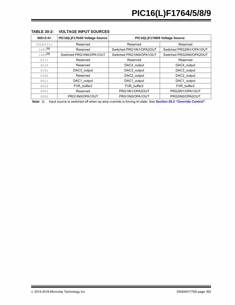
2014-2018 Microchip Technology Inc. DS40001775D-page 362
PIC16(L)F1764/5/8/9
TABLE 30-2: VOLTAGE INPUT SOURCES
INS<2:0> PIC16(L)F1764/5 Voltage Source PIC16(L)F1768/9 Voltage Source
1010-1111 Reserved Reserved Reserved
1001(1) Reserved Switched PRG1IN1/OPA2OUT Switched PRG2IN1/OPA1OUT
1000(1) Switched PRG1IN0/OPA1OUT Switched PRG1IN0/OPA1OUT Switched PRG2IN0/OPA2OUT
0111 Reserved Reserved Reserved
0110 Reserved DAC4_output DAC4_output
0101 DAC3_output DAC3_output DAC3_output
0100 Reserved DAC2_output DAC2_output
0011 DAC1_output DAC1_output DAC1_output
0010 FVR_buffer2 FVR_buffer2 FVR_buffer2
0001 Reserved PRG1IN1/OPA2OUT PRG2IN1/OPA1OUT
0000 PRG1IN0/OPA1OUT PRG1IN0/OPA1OUT PRG2IN0/OPA2OUT
Note 1: Input source is switched off when op amp override is forcing tri-state. See Section 29.3 “Override Control”.

2014-2018 Microchip Technology Inc. DS40001775D-page 363
PIC16(L)F1764/5/8/9
REGISTER 30-4: PRGxCON2: PROGRAMMABLE RAMP GENERATOR x CONTROL 2 REGISTER
R/W-0/0 U-0 U-0 R/W-0/0 R/W-0/0 R/W-0/0 R/W-0/0 R/W-0/0
LR(1) — — ISET<4:0>
bit 7 bit 0
Legend:
R = Readable bit W = Writable bit
u = Bit is unchanged x = Bit is unknown U = Unimplemented bit, read as ‘0’
‘1’ = Bit is set ‘0’ = Bit is cleared -n/n = Value at POR and BOR/Value at all other Resets
bit 7 LR: PRG Current Source/Sink Low Range Enable bit(1)
bit 6-5 Unimplemented: Read as ‘0’
bit 4-0 ISET<4:0>: PRG Current Source/Sink Set bits
Current source/sink setting and slope rate. See Table 30-3.
Note 1: Available on PIC16(L)F1768/9 only.

2014-2018 Microchip Technology Inc. DS40001775D-page 364
PIC16(L)F1764/5/8/9
TABLE 30-3: PROGRAMMABLE RAMP GENERATOR CURRENT SETTINGS
ISET<4:1>
LR = 0 LR = 1
Current Setting(A)
Slope Rate(V/s)
Current Setting(A)
Slope Rate(V/s)
0h 2 0.2 0.44 0.04
1h 2.5 0.25 0.56 0.06
2h 3 0.3 0.67 0.07
3h 3.5 0.35 0.78 0.08
4h 4 0.4 0.89 0.09
5h 4.5 0.45 1.00 0.10
6h 5 0.5 1.11 0.11
7h 5.5 0.55 1.22 0.12
8h 6 0.6 1.33 0.13
9h 6.5 0.65 1.44 0.14
Ah 7 0.7 1.56 0.16
Bh 7.5 0.75 1.67 0.17
Ch 8 0.8 1.78 0.18
Dh 8.5 0.85 1.89 0.19
Eh 9 0.9 2.00 0.20
Fh 9.5 0.95 2.11 0.21
10h 10 1.0 2.22 0.22
11h 11 1.1 2.44 0.24
12h 12 1.2 2.67 0.27
13h 13 1.3 2.89 0.29
14h 14 1.4 3.11 0.31
15h 15 1.5 3.33 0.33
16h 16 1.6 3.56 0.36
17h 17 1.7 3.78 0.38
18h 18 1.8 4.00 0.40
19h 19 1.9 4.22 0.42
1Ah 20 2.0 4.44 0.44
1Bh 21 2.1 4.67 0.47
1Ch 22 2.2 4.89 0.49
1Dh 23 2.3 5.11 0.51
1Eh 24 2.4 5.33 0.53
1Fh 25 2.5 5.56 0.56

2014-2018 Microchip Technology Inc. DS40001775D-page 365
PIC16(L)F1764/5/8/9
REGISTER 30-5: PRGxRTSS: PRGx set_rising TIMING SOURCE SELECT REGISTER
U-0 U-0 U-0 U-0 R/W-0/0 R/W-0/0 R/W-0/0 R/W-0/0
— — — — RTSS<3:0>
bit 7 bit 0
Legend:
R = Readable bit W = Writable bit
u = Bit is unchanged x = Bit is unknown U = Unimplemented bit, read as ‘0’
‘1’ = Bit is set ‘0’ = Bit is cleared -n/n = Value at POR and BOR/Value at all other Resets
bit 7-4 Unimplemented: Read as ‘0’
bit 3-0 RTSS<3:0>: set_rising Timing Source Select bits
See Table 30-4.
REGISTER 30-6: PRGxFTSS: PRGx set_falling TIMING SOURCE SELECT REGISTER
U-0 U-0 U-0 U-0 R/W-0/0 R/W-0/0 R/W-0/0 R/W-0/0
— — — — FTSS<3:0>
bit 7 bit 0
Legend:
R = Readable bit W = Writable bit
u = Bit is unchanged x = Bit is unknown U = Unimplemented bit, read as ‘0’
‘1’ = Bit is set ‘0’ = Bit is cleared -n/n = Value at POR and BOR/Value at all other Resets
bit 7-4 Unimplemented: Read as ‘0’
bit 3-0 FTSS<3:0>: set_falling Timing Source Select bits
See Table 30-4.
TABLE 30-4: PROGRAMMABLE RAMP GENERATOR TIMING SOURCES
RTSS<3:0>/FTSS<3:0> Timing Source RTSS<3:0>/FTSS<3:0> Timing Source
0000 sync_C1OUT 1000 PWM6_output(2)
0001 sync_C2OUT 1001 CCP1_out
0010 sync_C3OUT(2) 1010 CCP2_out(2)
0011 sync_C4OUT(2) 1011 Reserved
0100 PRGxR/PRGxF Pin(1) 1100 Reserved
0101 PWM3_output 1101 Reserved
0110 PWM4_output(2) 1110 Reserved
0111 PWM5_output 1111 Reserved
Note 1: Input pin is selected with the PRGxRPPS or PRGxFPPS register.
2: PIC16(L)F1768/9 only.

2014-2018 Microchip Technology Inc. DS40001775D-page 366
PIC16(L)F1764/5/8/9
TABLE 30-5: SUMMARY OF REGISTERS ASSOCIATED WITH THE PRG MODULE
Name Bit 7 Bit 6 Bit 5 Bit 4 Bit 3 Bit 2 Bit 1 Bit 0Register on Page
PRG1CON0 EN — FEDG REDG MODE<1:0> OS GO 360
PRG1CON1 — — — — — RDY FPOL RPOL 361
PRG1CON2 LR(2) — — ISET<4:0> 363
PRG1INS — — — — INS<3:0> 361
PRG1RPPS — — — PRG1RPPS<4:0> 365
PRG1FPPS — — — PRG1FPPS<4:0> 365
PRG1RTSS — — — — RTSS<3:0> 154, 156
PRG1FTSS — — — — FTSS<3:0> 154, 156
PRG2CON0(1) EN — FEDG REDG MODE<1:0> OS GO 360
PRG2CON1(1) — — — — — RDY FPOL RPOL 361
PRG2CON2(1) LR — — ISET<4:0> 363
PRG2INS(1) — — — — INS<3:0> 361
PRG2RPPS(1) — — — PRG2RPPS<4:0> 365
PRG2FPPS(1) — — — PRG2FPPS<4:0> 365
PRG2RTSS(1) — — — — RTSS<3:0> 154, 156
PRG2FTSS(1) — — — — FTSS<3:0> 154, 156
PORTC RC<7:6>(1) RC<5:0> 147
TRISC TRISC<7:6>(1) TRISC<5:4> TRISC<3:2> TRISC<1:0> 147
ANSELC ANSC<7:6>(1) — — ANSC<3:2> ANSC<1:0> 148
WPUC WPUC<7:6>(1) WPUC<5:4> WPUC<3:2> WPUC<1:0> 149
Legend: — = unimplemented, read as ‘0’. Shaded cells are unused by the PRG module.Note 1: PIC16(L)F1768/9 only.

2014-2018 Microchip Technology Inc. DS40001775D-page 367
PIC16(L)F1764/5/8/9
31.0 DATA SIGNAL MODULATOR (DSM)
The Data Signal Modulator (DSM) is a peripheral thatallows the user to mix a data stream, also known as amodulator signal, with a carrier signal to produce amodulated output.
Both the carrier and the modulator signals are suppliedto the DSM module either internally, from the output ofa peripheral, or externally through an input pin.
The modulated output signal is generated by performinga logical “AND” operation of both the carrier andmodulator signals and then provided to the MDxOUT pin.
The carrier signal is comprised of two distinct and sepa-rate signals: a Carrier High (CARH) signal and a CarrierLow (CARL) signal. During the time in which the Modu-lator (MOD) signal is in a logic high state, the DSM mixesthe Carrier High signal with the Modulator signal. Whenthe Modulator signal is in a logic low state, the DSMmixes the Carrier Low signal with the Modulator signal.
Using this method, the DSM can generate the followingtypes of key modulation schemes:
• Frequency-Shift Keying (FSK)
• Phase-Shift Keying (PSK)
• On-Off Keying (OOK)
Additionally, the following features are provided withinthe DSM module:
• Carrier Synchronization
• Carrier Source Polarity Select
• Carrier Source Pin Disable
• Programmable Modulator Data
• Modulator Source Pin Disable
• Modulated Output Polarity Select
• Slew Rate Control
Figure 31-1 shows a simplified block diagram of theData Signal Modulator peripheral.
FIGURE 31-1: SIMPLIFIED BLOCK DIAGRAM OF THE DATA SIGNAL MODULATOR
D
Q
MDxCHPPS
MDxCLPPS
CH<3:0>
MS<3:0>
CL<3:0>
SYNC
CHPOL
CLPOL
D
Q 1
0
SYNC
1
0
CHSYNC
CLSYNC
MDxOUT
OPOL
CARH
CARL
EN
Data SignalModulator
MOD
PPS
RxyPPS
Carrier High Sources,See Table 31-4
Modulation Sources,See Table 31-3
Carrier Low Sources,See Table 31-5
PPS
PPS
PPS
MDx_out
MDxMODPPS

2014-2018 Microchip Technology Inc. DS40001775D-page 368
PIC16(L)F1764/5/8/9
31.1 DSM Operation
The DSM module is enabled by setting the EN bit in theMDxCON register. Clearing the EN bit in the MDxCONregister, disables the DSM module by automaticallyswitching the Carrier High and Carrier Low signals tothe VSS signal source. The Modulator signal source isalso switched to the BIT bit in the MDxCON0 register.This not only assures that the DSM module is inactive,but that it is also consuming the least amount ofcurrent.
The values used to select the Carrier High, Carrier Lowand Modulator sources held by the Modulation Source,Modulation High Carrier and Modulation Low Carrierregisters are not affected when the EN bit is cleared,and the DSM module is disabled. The values insidethese registers remain unchanged while the DSM isinactive. The sources for the Carrier High, Carrier Lowand Modulator signals will once again be selectedwhen the EN bit is set and the DSM module is enabledand active.
The modulated output signal can be output on anydevice I/O pin by selecting the desired DSM module inthe pin’s PPS Control register (see Register 12-2). Ifthe output is not directed to any I/O pin, then the DSMmodule will remain active and continue to mix signals,but the output value will not be sent to any pin.
31.2 Modulator Signal Sources
The Modulator signal is selected by configuring theMS<4:0> bits of the MDxSRC register. Selections areshown in Table 31-3.
31.3 Carrier Signal Sources
The Carrier High signal is selected by configuring theCH<3:0> bits of the MDxCARH register. Selections areshown in Table 31-4.
The Carrier Low signal is selected by configuring theCL<3:0> bits of the MDxCARL register. Selections areshown in Table 31-5.
31.4 Carrier Synchronization
During the time when the DSM switches between Car-rier High and Carrier Low signal sources, the carrierdata in the modulated output signal can becometruncated. To prevent this, the carrier signal can besynchronized to the Modulator signal. When synchroni-zation is enabled, the carrier pulse that is being mixedat the time of the transition is allowed to transition lowbefore the DSM switches over to the next carriersource.
Synchronization is enabled separately for the CarrierHigh and Carrier Low signal sources. Synchronizationfor the Carrier High signal is enabled by setting theCHSYNC bit of the MDxCON1 register. Synchroniza-tion for the Carrier Low signal is enabled by setting theCLSYNC bit of the MDxCON1 register.
Figure 31-1 through Figure 31-6 show timing diagramsof using various synchronization methods.

2014-2018 Microchip Technology Inc. DS40001775D-page 369
PIC16(L)F1764/5/8/9
FIGURE 31-2: ON-OFF KEYING (OOK) SYNCHRONIZATION
FIGURE 31-3: NO SYNCHRONIZATION (MDCHSYNC = 0, MDCLSYNC = 0)
FIGURE 31-4: CARRIER HIGH SYNCHRONIZATION (MDCHSYNC = 1, MDCLSYNC = 0)
Carrier Low (CARL)
1 x MDx_out
0 x MDx_out
Carrier High (CARH)
Modulator (MOD)
MDCLSYNC
MDCHSYNC
MDx_out
Modulator (MOD)
Carrier High (CARH)
Carrier Low (CARL)
Active Carrier CARH CARL CARLCARHState
MDx_out
Modulator (MOD)
Carrier High (CARH)
Carrier Low (CARL)
Active Carrier CARH CARL CARLCARHState both both

2014-2018 Microchip Technology Inc. DS40001775D-page 370
PIC16(L)F1764/5/8/9
FIGURE 31-5: CARRIER LOW SYNCHRONIZATION (MDCHSYNC = 0, MDCLSYNC = 1)
FIGURE 31-6: FULL SYNCHRONIZATION (MDCHSYNC = 1, MDCLSYNC = 1)
MDx_out
Modulator (MOD)
Carrier High (CARH)
Carrier Low (CARL)
Active Carrier CARH CARL CARLCARHState
MDx_out
Modulator (MOD)
Carrier High (CARH)
Carrier Low (CARL)
Active Carrier CARH CARL CARLCARHState
Falling EdgesUsed to Sync

2014-2018 Microchip Technology Inc. DS40001775D-page 371
PIC16(L)F1764/5/8/9
31.5 Input and Output Through Pins
The modulation and carrier sources may be selected tocome from any device pin with the PPS control logic.Selecting a pin requires two settings: the source selec-tion determines that the PPS will be used and the PPScontrol selects the desired pin. Source and PPS registersare identified in Table 31-1. PPS register pin selectionsare shown in Register 12-1 and Register 12-2.
Any device pin can be selected as the modulationoutput with the individual pin PPS controls. SeeRegister 12-2 for the pin output selections.
31.6 Carrier Source Polarity Select
The signal provided from any selected input source forthe Carrier High and Carrier Low signals can beinverted. Inverting the signal for the Carrier High sourceis enabled by setting the CHPOL bit of the MDxCON1register. Inverting the signal for the Carrier Low sourceis enabled by setting the CLPOL bit of the MDxCON1register.
31.7 Programmable Modulator Data
The BIT bit of the MDxCON0 register can be selectedas the source for the Modulator signal. When the BITsource is selected, then software generates the Modu-lation signal by setting and clearing the BIT bit at therespective desired modulation high and low times.
31.8 Modulated Output Polarity
The modulated output signal provided on the MDxOUTpin can also be inverted. Inverting the modulated out-put signal is enabled by setting the OPOL bit of theMDxCON0 register.
31.9 Operation in Sleep Mode
The DSM module is not affected by Sleep mode. TheDSM will operate during Sleep provided that the carrierand modulator input sources are also active duringSleep.
31.10 Effects of a Reset
Upon any device Reset, the Data Signal Modulatormodule is disabled. The user’s firmware is responsiblefor initializing the module before enabling the output.The registers are reset to their default values.
TABLE 31-1: PIN SELECTIONS
SourceSource
RegisterPPS Register
Modulation MDxSRC MDxMODPPS
Carrier High MDxCARH MDxCHPPS
Carrier Low MDxCARL MDxCLPPS

2014-2018 Microchip Technology Inc. DS40001775D-page 372
PIC16(L)F1764/5/8/9
31.11 Register Definitions: Data Signal Modulator
Long bit name prefixes for the DSM peripherals areshown in Table 31-2. Refer to Section 1.1.2.2 “LongBit Names” for more information.
TABLE 31-2: BIT NAME PREFIXES
Peripheral Bit Name Prefix
DSM1 MD1
DSM2(1) MD2
Note 1: PIC16(L)F1768/9 devices only.
REGISTER 31-1: MDxCON0: MODULATION x CONTROL REGISTER 0
R/W-0/0 U-0 R-0/0 R/W-0/0 U-0 U-0 U-0 R/W-0/0
EN — OUT OPOL — — — BIT(2)
bit 7 bit 0
Legend:
R = Readable bit W = Writable bit
u = Bit is unchanged x = Bit is unknown U = Unimplemented bit, read as ‘0’
‘1’ = Bit is set ‘0’ = Bit is cleared -n/n = Value at POR and BOR/Value at all other Resets
bit 7 EN: Modulator Module Enable bit
1 = Modulator module is enabled and mixing input signals0 = Modulator module is disabled and has no output
bit 6 Unimplemented: Read as ‘0’
bit 5 OUT: Modulator Output bit
Displays the current output value of the modulator module.(1)
bit 4 OPOL: Modulator Output Polarity Select bit
1 = Modulator output signal is inverted; Idle high output0 = Modulator output signal is not inverted; Idle low output
bit 3-1 Unimplemented: Read as ‘0’
bit 0 BIT: Direct Software Control of the Modulation Source Input to Module bit(2)
1 = Modulator uses Carrier High source0 = Modulator uses Carrier Low source
Note 1: The modulated output frequency can be greater and asynchronous from the clock that updates this register bit; the bit value may not be valid for higher speed modulator or carrier signals.
2: BIT must be selected as the modulation source in the MDxSRC register for this operation.

2014-2018 Microchip Technology Inc. DS40001775D-page 373
PIC16(L)F1764/5/8/9
REGISTER 31-2: MDxCON1: MODULATION x CONTROL REGISTER 1
U-0 U-0 R/W-0/0 R/W-0/0 U-0 U-0 R/W-0/0 R/W-0/0
— — CHPOL CHSYNC — — CLPOL CLSYNC
bit 7 bit 0
Legend:
R = Readable bit W = Writable bit
u = Bit is unchanged x = Bit is unknown U = Unimplemented bit, read as ‘0’
‘1’ = Bit is set ‘0’ = Bit is cleared -n/n = Value at POR and BOR/Value at all other Resets
bit 7-6 Unimplemented: Read as ‘0’
bit 5 CHPOL: Modulation High Carrier Polarity Select bit
1 = Selected high carrier source is inverted0 = Selected high carrier source is not inverted
bit 4 CHSYNC: Modulation High Carrier Synchronization Enable bit
1 = Modulator waits for a low edge on the high carrier before allowing a switch to the low carrier0 = Modulator output is not synchronized to the high carrier(1)
bit 3-2 Unimplemented: Read as ‘0’
bit 1 CLPOL: Modulation Low Carrier Polarity Select bit
1 = Selected low carrier source is inverted0 = Selected low carrier source is not inverted
bit 0 CLSYNC: Modulation Low Carrier Synchronization Enable bit
1 = Modulator waits for a low edge on the low carrier before allowing a switch to the high carrier0 = Modulator output is not synchronized to the low carrier(1)
Note 1: Narrowed carrier pulse widths or spurs may occur in the signal stream if the carrier is not synchronized.

2014-2018 Microchip Technology Inc. DS40001775D-page 374
PIC16(L)F1764/5/8/9
REGISTER 31-3: MDxSRC: MODULATION x SOURCE CONTROL REGISTER
U-0 U-0 U-0 R/W-x/u R/W-x/u R/W-x/u R/W-x/u R/W-x/u
— — — MS<4:0>
bit 7 bit 0
Legend:
R = Readable bit W = Writable bit
u = Bit is unchanged x = Bit is unknown U = Unimplemented bit, read as ‘0’
‘1’ = Bit is set ‘0’ = Bit is cleared -n/n = Value at POR and BOR/Value at all other Resets
bit 7-5 Unimplemented: Read as ‘0’
bit 4-0 MS<4:0> Modulation Source Selection bits
See Table 31-3.
TABLE 31-3: MODULATION SOURCE
MS<4:0>Modulation Source
PIC16(L)F1764/5Modulation Source
PIC16(L)F1768/9
11111-10100 Fixed Low Fixed Low
10011 Fixed Low sync_C4OUT
10010 Fixed Low sync_C3OUT
10001 sync_C2OUT sync_C2OUT
10000 sync_C1OUT sync_C1OUT
01111 LC3_out LC3_out
01110 LC2_out LC2_out
01101 LC1_out LC1_out
01100 Fixed Low PWM6_out
01011 PWM5_out PWM5_out
01010 Fixed Low PWM4_out
01001 PWM3_out PWM3_out
01000 Fixed low CCP2_out
00111 CCP1_out CCP1_out
00110 SDO_out SDO_out
00101 Fixed Low COG2A
00100 DT DT
00011 TX_out TX_out
00010 COG1A COG1A
00001 MDxBIT MDxBIT
00000 MDxMODPPS Pin Selection MDxMODPPS Pin Selection

2014-2018 Microchip Technology Inc. DS40001775D-page 375
PIC16(L)F1764/5/8/9
REGISTER 31-4: MDxCARH: MODULATION x CARRIER HIGH CONTROL REGISTER
U-0 U-0 U-0 U-0 R/W-x/u R/W-x/u R/W-x/u R/W-x/u
— — — — CH<3:0>(1)
bit 7 bit 0
Legend:
R = Readable bit W = Writable bit
u = Bit is unchanged x = Bit is unknown U = Unimplemented bit, read as ‘0’
‘1’ = Bit is set ‘0’ = Bit is cleared -n/n = Value at POR and BOR/Value at all other Resets
bit 7-4 Unimplemented: Read as ‘0’
bit 3-0 CH<3:0> Modulator Data High Carrier Selection bits(1)
See Table 31-4.
Note 1: Narrowed carrier pulse widths or spurs may occur in the signal stream if the carrier is not synchronized.
TABLE 31-4: HIGH CARRIER SOURCES
CH<3:0>High Carrier Source
PIC16(L)F1764/5High Carrier Source
PIC16(L)F1768/9
1111 LC3_out LC3_out
1110 LC2_out LC2_out
1101 LC1_out LC1_out
1100 Fixed Low PWM6_out
1011 PWM5_out PWM5_out
1010 Fixed Low PWM4_out
1001 PWM3_out PWM3_out
1000 Fixed Low CCP2_out
0111 CCP1_out CCP1_out
0110 Fixed Low Fixed Low
0101 Fixed Low Fixed Low
0100 Fixed Low Fixed Low
0011 Fixed Low Fixed Low
0010 HFINTOSC HFINTOSC
0001 FOSC FOSC
0000 MDxCHPPS Pin Selection MDxCHPPS Pin Selection

2014-2018 Microchip Technology Inc. DS40001775D-page 376
PIC16(L)F1764/5/8/9
TABLE 31-6: SUMMARY OF REGISTERS ASSOCIATED WITH DATA SIGNAL MODULATOR MODE
REGISTER 31-5: MDxCARL: MODULATION x CARRIER LOW CONTROL REGISTER
U-0 U-0 U-0 U-0 R/W-x/u R/W-x/u R/W-x/u R/W-x/u
— — — — CL<3:0>(1)
bit 7 bit 0
Legend:
R = Readable bit W = Writable bit U = Unimplemented bit, read as ‘0’
u = Bit is unchanged x = Bit is unknown -n/n = Value at POR and BOR/Value at all other Resets
‘1’ = Bit is set ‘0’ = Bit is cleared
bit 7-4 Unimplemented: Read as ‘0’
bit 3-0 CL<3:0> Modulator Data Low Carrier Selection bits(1)
See Table 31-5.
Note 1: Narrowed carrier pulse widths or spurs may occur in the signal stream if the carrier is not synchronized.
TABLE 31-5: LOW CARRIER SOURCES
CL<3:0>Low Carrier Source
PIC16(L)F1764/5Low Carrier Source
PIC16(L)F1768/9
1111 LC3_out LC3_out
1110 LC2_out LC2_out
1101 LC1_out LC1_out
1100 Fixed Low PWM6_out
1011 PWM5_out PWM5_out
1010 Fixed Low PWM4_out
1001 PWM3_out PWM3_out
1000 Fixed Low CCP2_out
0111 CCP1_out CCP1_out
0110 Fixed Low Fixed Low
0101 Fixed Low Fixed Low
0100 Fixed Low Fixed Low
0011 Fixed Low Fixed Low
0010 HFINTOSC HFINTOSC
0001 FOSC FOSC
0000 MDxCLPPS Pin Selection MDxCLPPS Pin Selection
Name Bit 7 Bit 6 Bit 5 Bit 4 Bit 3 Bit 2 Bit 1 Bit 0Register on Page
MDxCARH — — — — CH<3:0> 375
MDxCARL — — — — CL<3:0> 376
MDxSRC — — — MS<4:0> 373
MDxCON0 EN — OUT OPOL — — — BIT 372
MDxCON1 — — CHPOL CHSYNC — — CLPOL CLSYNC 372
Legend: — = unimplemented location, read as ‘0’. Shaded cells are not used by the Data Signal Modulator.

2014-2018 Microchip Technology Inc. DS40001775D-page 377
PIC16(L)F1764/5/8/9
32.0 MASTER SYNCHRONOUS SERIAL PORT (MSSP) MODULE
32.1 MSSP Module Overview
The Master Synchronous Serial Port (MSSP) module isa serial interface useful for communicating with otherperipheral or microcontroller devices. These peripheraldevices may be serial EEPROMs, shift registers,display drivers, A/D converters, etc. The MSSP modulecan operate in one of two modes:
• Serial Peripheral Interface (SPI)
• Inter-Integrated Circuit (I2C)
The SPI interface supports the following modes andfeatures:
• Master mode
• Slave mode
• Clock Parity
• Slave Select Synchronization (Slave mode only)
• Daisy-Chain Connection of Slave Devices
Figure 32-1 is a block diagram of the SPI interfacemodule.
FIGURE 32-1: MSSP BLOCK DIAGRAM (SPI MODE)
( )
Read Write
Data Bus
SSPSR Reg
SSPM<3:0>
bit 0 ShiftClock
SS ControlEnable
EdgeSelect
Clock Select
T2_match2
EdgeSelect
2 (CKP, CKE)
4
TRISx bit
SDO
SSPxBUF Reg
SDI
SS
SCK
TOSCPrescaler4, 16, 64
Baud RateGenerator
(SSPxADD)
PPS
PPS
PPS
PPS
SSPDATPPS
RxyPPS
SSPCLKPPS(2)
PPS
RxyPPS(1)
SSPSSPPS
Note 1: Output selection for Master mode.2: Input selection for Slave and Master modes.

2014-2018 Microchip Technology Inc. DS40001775D-page 378
PIC16(L)F1764/5/8/9
The I2C interface supports the following modes andfeatures:
• Master mode• Slave mode• Byte NACKing (Slave mode)• Limited multi-master support• 7-Bit and 10-Bit Addressing• Start and Stop interrupts• Interrupt masking• Clock stretching• Bus collision detection• General call address matching• Address masking• Address Hold and Data Hold modes• Selectable SDA hold times
Figure 32-2 is a block diagram of the I2C interfacemodule in Master mode. Figure 32-3 is a diagram of theI2C interface module in Slave mode.
FIGURE 32-2: MSSP BLOCK DIAGRAM (I2C MASTER MODE)
Read Write
SSPSR
Start bit, Stop bit,
Start bit Detect,
SSPxBUF
InternalData Bus
Set/Reset: S, P, SSPxSTAT, WCOL, SSPOV;
ShiftClock
MSb LSb
SDA
AcknowledgeGenerate (SSPxCON2)
Stop bit Detect,Write Collision Detect,
Clock Arbitration,State Counter for
End of XMIT/RCV,
SCL
SCL In
Bus Collision
SDA In
Rec
eive
Ena
ble
(RC
EN
)
Clo
ck C
ntl
Clo
ck A
rbitr
ate
/BC
OL
De
tect
(ho
ld o
ff cl
ock
so
urce
)
[SSPM<3:0>]
Baud Rate
Reset SEN, PEN (SSPxCON2);
Generator(SSPxADD)
Address Match Detect
Set SSP1IF, BCL1IF
PPS
SSPDATPPS(1)
PPS
Note 1: SDA pin selections must be the same for input and output.2: SCL pin selections must be the same for input and output.
PPS
PPS
SSPCLKPPS(2)
RxyPPS(1)
RxyPPS(2)

2014-2018 Microchip Technology Inc. DS40001775D-page 379
PIC16(L)F1764/5/8/9
FIGURE 32-3: MSSP BLOCK DIAGRAM (I2C SLAVE MODE)
Read Write
SSPSR Reg
Match Detect
SSPxADD Reg
Start andStop bit Detect
SSPxBUF Reg
InternalData Bus
Addr Match
Set, ResetS, P bits(SSPxSTAT Reg)
SCL
ShiftClock
MSb LSb
SSPxMSK Reg
PPS
PPS
SSPCLKPPS(2)
RxyPPS(2)
Clock Stretching
SDA
PPS
PPS
SSPDATPPS(1)
RxyPPS(1)
Note 1: SDA pin selections must be the same for input and output.2: SCL pin selections must be the same for input and output.

2014-2018 Microchip Technology Inc. DS40001775D-page 380
PIC16(L)F1764/5/8/9
32.2 SPI Mode Overview
The Serial Peripheral Interface (SPI) bus is asynchronous serial data communication bus thatoperates in Full-Duplex mode. Devices communicatein a master/slave environment where the master deviceinitiates the communication. A slave device iscontrolled through a chip select known as Slave Select.
The SPI bus specifies four signal connections:
• Serial Clock (SCK)
• Serial Data Out (SDO)
• Serial Data In (SDI)
• Slave Select (SS)
Figure 32-1 shows the block diagram of the MSSPmodule when operating in SPI mode.
The SPI bus operates with a single master device andone or more slave devices. When multiple slavedevices are used, an independent Slave Selectconnection is required from the master device to eachslave device.
Figure 32-4 shows a typical connection between amaster device and multiple slave devices.
The master selects only one slave at a time. Most slavedevices have tri-state outputs so their output signalappears disconnected from the bus when they are notselected.
Transmissions involve two shift registers, eight bits insize, one in the master and one in the slave. With eitherthe master or the slave device, data is always shiftedout one bit at a time, with the Most Significant bit (MSb)shifted out first. At the same time, a new LeastSignificant bit (LSb) is shifted into the same register.
Figure 32-5 shows a typical connection between twoprocessors configured as master and slave devices.
Data is shifted out of both shift registers on theprogrammed clock edge and latched on the oppositeedge of the clock.
The master device transmits information out on its SDOoutput pin, which is connected to, and received by, theslave’s SDI input pin. The slave device transmits infor-mation out on its SDO output pin, which is connectedto, and received by, the master’s SDI input pin.
To begin communication, the master device first sendsout the clock signal. Both the master and the slavedevices should be configured for the same clock polarity.
The master device starts a transmission by sending outthe MSb from its shift register. The slave device readsthis bit from that same line and saves it into the LSbposition of its shift register.
During each SPI clock cycle, a full-duplex datatransmission occurs. This means that while the masterdevice is sending out the MSb from its shift register (onits SDO pin), and the slave device is reading this bit andsaving it as the LSb of its shift register, that the slavedevice is also sending out the MSb from its shift register(on its SDO pin) and the master device is reading thisbit and saving it as the LSb of its shift register.
After eight bits have been shifted out, the master andslave have exchanged register values.
If there is more data to exchange, the shift registers areloaded with new data and the process repeats itself.
Whether the data is meaningful or not (dummy data),depends on the application software. This leads tothree scenarios for data transmission:
• Master sends useful data and slave sends dummy data.
• Master sends useful data and slave sends useful data.
• Master sends dummy data and slave sends useful data.
Transmissions may involve any number of clockcycles. When there is no more data to be transmitted,the master stops sending the clock signal and itdeselects the slave.
Every slave device connected to the bus that has notbeen selected through its Slave Select line mustdisregard the clock and transmission signals and mustnot transmit out any data of its own.

2014-2018 Microchip Technology Inc. DS40001775D-page 381
PIC16(L)F1764/5/8/9
FIGURE 32-4: SPI MASTER AND MULTIPLE SLAVE CONNECTION
32.2.1 SPI MODE REGISTERS
The MSSP module has five registers for SPI modeoperation. These are:
• MSSP Status Register (SSPxSTAT)
• MSSP Control Register 1 (SSPxCON1)
• MSSP Control Register 3 (SSPxCON3)
• MSSP Data Buffer Register (SSPxBUF)
• MSSP Address Register (SSPxADD)
• MSSP Shift Register (SSPSR) (Not directly accessible)
SSPxCON1 and SSPxSTAT are the control andSTATUS registers in SPI mode operation. TheSSPxCON1 register is readable and writable. Thelower six bits of the SSPxSTAT are read-only. Theupper two bits of the SSPxSTAT are read/write.
In one SPI Master mode, SSPxADD can be loadedwith a value used in the Baud Rate Generator. Moreinformation on the Baud Rate Generator is available inSection 32.7 “Baud Rate Generator”.
SSPSR is the shift register used for shifting data in andout. SSPxBUF provides indirect access to the SSPSRregister. SSPxBUF is the buffer register to which databytes are written, and from which data bytes are read.
In receive operations, SSPSR and SSPxBUF togethercreate a buffered receiver. When SSPSR receives acomplete byte, it is transferred to SSPxBUF and theSSPxIF interrupt is set.
During transmission, the SSPxBUF is not buffered. Awrite to SSPxBUF will write to both SSPxBUF andSSPSR.
32.2.2 SPI MODE OPERATION
When initializing the SPI, several options need to bespecified. This is done by programming the appropriatecontrol bits (SSPxCON1<5:0> and SSPxSTAT<7:6>).These control bits allow the following to be specified:
• Master mode (SCK is the clock output)• Slave mode (SCK is the clock input)• Clock Polarity (Idle state of SCK)• Data Input Sample Phase (middle or end of data
output time)• Clock Edge (output data on rising/falling edge of
SCK)• Clock Rate (Master mode only)• Slave Select mode (Slave mode only)
To enable the serial port, SSP Enable bit, SSPEN of theSSPxCON1 register, must be set. To reset or reconfigureSPI mode, clear the SSPEN bit, re-initialize theSSPxCONx registers and then set the SSPEN bit. Thisconfigures the SDI, SDO, SCK and SS pins as serial portpins. For the pins to behave as the serial port function,some must have their data direction bits (in the TRISxregister) appropriately programmed as follows:
• SDI must have corresponding TRISx bit set • SDO must have corresponding TRISx bit cleared• SCK (Master mode) must have corresponding
TRISx bit cleared• SCK (Slave mode) must have corresponding
TRISx bit set • SS must have corresponding TRISx bit set
Any serial port function that is not desired may beoverridden by programming the corresponding DataDirection (TRISx) register to the opposite value.
SPI MasterSCK
SDO
SDI
General I/OGeneral I/O
General I/O
SCK
SDI
SDO
SS
SPI Slave#1
SCK
SDI
SDO
SS
SPI Slave#2
SCK
SDI
SDO
SS
SPI Slave#3

2014-2018 Microchip Technology Inc. DS40001775D-page 382
PIC16(L)F1764/5/8/9
The MSSP consists of a transmit/receive shift register(SSPSR) and a buffer register (SSPxBUF). TheSSPSR shifts the data in and out of the device, MSbfirst. The SSPxBUF holds the data that was written tothe SSPSR until the received data is ready. Once theeight bits of data have been received, that byte ismoved to the SSPxBUF register. Then, the Buffer FullDetect bit, BF of the SSPxSTAT register, and the inter-rupt flag bit, SSPxIF, are set. This double-buffering ofthe received data (SSPxBUF) allows the next byte tostart reception before reading the data that was justreceived. Any write to the SSPxBUF register duringtransmission/reception of data will be ignored and theWrite Collision Detect bit, WCOL of the SSPxCON1register, will be set. User software must clear theWCOL bit to allow the following write(s) to theSSPxBUF register to complete successfully.
When the application software is expecting to receivevalid data, the SSPxBUF should be read before thenext byte of data to transfer is written to the SSPxBUF.The Buffer Full bit, BF of the SSPxSTAT register,indicates when SSPxBUF has been loaded with thereceived data (transmission is complete). When theSSPxBUF is read, the BF bit is cleared. This data maybe irrelevant if the SPI is only a transmitter. Generally,the MSSP interrupt is used to determine when thetransmission/reception has completed. If the interruptmethod is not going to be used, then software pollingcan be done to ensure that a write collision does notoccur.
The SSPSR is not directly readable or writable and canonly be accessed by addressing the SSPxBUF register.Additionally, the SSPxSTAT register indicates thevarious Status conditions.
FIGURE 32-5: SPI MASTER/SLAVE CONNECTION
Serial Input Buffer(BUF)
Shift Register(SSPSR)
MSb LSb
SDO
SDI
Processor 1
SCK
SPI Master SSPM<3:0> = 00xx
Serial Input Buffer(SSPxBUF)
Shift Register(SSPSR)
LSbMSb
SDI
SDO
Processor 2
SCK
SPI Slave SSPM<3:0> = 010x
Serial Clock
SSSlave Select
General I/O(optional)
= 1010

2014-2018 Microchip Technology Inc. DS40001775D-page 383
PIC16(L)F1764/5/8/9
32.2.3 SPI MASTER MODE
The master can initiate the data transfer at any timebecause it controls the SCK line. The masterdetermines when the slave (Processor 2, Figure 32-5)is to broadcast data by the software protocol.
In Master mode, the data is transmitted/received assoon as the SSPxBUF register is written to. If the SPIis only going to receive, the SDO output could bedisabled (programmed as an input). The SSPSRregister will continue to shift in the signal present on theSDI pin at the programmed clock rate. As each byte isreceived, it will be loaded into the SSPxBUF register asif a normal received byte (interrupts and status bitsappropriately set).
The clock polarity is selected by appropriatelyprogramming the CKP bit of the SSPxCON1 registerand the CKE bit of the SSPxSTAT register. This then,would give waveforms for SPI communication asshown in Figure 32-6, Figure 32-8, Figure 32-9 andFigure 32-10, where the MSB is transmitted first. InMaster mode, the SPI clock rate (bit rate) is userprogrammable to be one of the following:
• FOSC/4 (or TCY)• FOSC/16 (or 4 * TCY)• FOSC/64 (or 16 * TCY)• Timer2 output/2 • FOSC/(4 * (SSPxADD + 1))
Figure 32-6 shows the waveforms for Master mode.
When the CKE bit is set, the SDO data is valid beforethere is a clock edge on SCK. The change of the inputsample is shown based on the state of the SMP bit. Thetime when the SSPxBUF is loaded with the receiveddata is shown.
Note: In Master mode, the clock signal output tothe SCK pin is also the clock signal inputto the peripheral. The pin selected for out-put with the RxyPPS register must also beselected as the peripheral input with theSSPCLKPPS register.
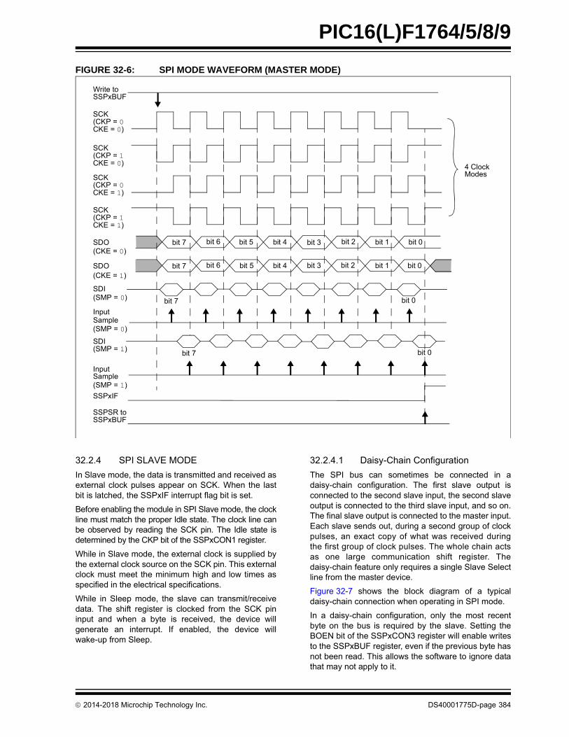
2014-2018 Microchip Technology Inc. DS40001775D-page 384
PIC16(L)F1764/5/8/9
FIGURE 32-6: SPI MODE WAVEFORM (MASTER MODE)
32.2.4 SPI SLAVE MODE
In Slave mode, the data is transmitted and received asexternal clock pulses appear on SCK. When the lastbit is latched, the SSPxIF interrupt flag bit is set.
Before enabling the module in SPI Slave mode, the clockline must match the proper Idle state. The clock line canbe observed by reading the SCK pin. The Idle state isdetermined by the CKP bit of the SSPxCON1 register.
While in Slave mode, the external clock is supplied bythe external clock source on the SCK pin. This externalclock must meet the minimum high and low times asspecified in the electrical specifications.
While in Sleep mode, the slave can transmit/receivedata. The shift register is clocked from the SCK pininput and when a byte is received, the device willgenerate an interrupt. If enabled, the device willwake-up from Sleep.
32.2.4.1 Daisy-Chain Configuration
The SPI bus can sometimes be connected in adaisy-chain configuration. The first slave output isconnected to the second slave input, the second slaveoutput is connected to the third slave input, and so on.The final slave output is connected to the master input.Each slave sends out, during a second group of clockpulses, an exact copy of what was received duringthe first group of clock pulses. The whole chain actsas one large communication shift register. Thedaisy-chain feature only requires a single Slave Selectline from the master device.
Figure 32-7 shows the block diagram of a typicaldaisy-chain connection when operating in SPI mode.
In a daisy-chain configuration, only the most recentbyte on the bus is required by the slave. Setting theBOEN bit of the SSPxCON3 register will enable writesto the SSPxBUF register, even if the previous byte hasnot been read. This allows the software to ignore datathat may not apply to it.
SCK(CKP = 0
SCK(CKP = 1
SCK(CKP = 0
SCK(CKP = 1
4 ClockModes
InputSample
InputSample
SDI
bit 7 bit 0
SDO bit 7 bit 6 bit 5 bit 4 bit 3 bit 2 bit 1 bit 0
bit 7
SDI
SSPxIF
(SMP = 1)
(SMP = 0)
(SMP = 1)
CKE = 1)
CKE = 0)
CKE = 1)
CKE = 0)
(SMP = 0)
Write toSSPxBUF
SSPSR toSSPxBUF
SDO bit 7 bit 6 bit 5 bit 4 bit 3 bit 2 bit 1 bit 0
(CKE = 0)
(CKE = 1)
bit 0

2014-2018 Microchip Technology Inc. DS40001775D-page 385
PIC16(L)F1764/5/8/9
32.2.5 SLAVE SELECT SYNCHRONIZATION
The Slave Select can also be used to synchronizecommunication. The Slave Select line is held high untilthe master device is ready to communicate. When theSlave Select line is pulled low, the slave knows that anew transmission is starting.
If the slave fails to receive the communication properly,it will be reset at the end of the transmission, when theSlave Select line returns to a high state. The slave isthen ready to receive a new transmission when theSlave Select line is pulled low again. If the Slave Selectline is not used, there is a risk that the slave willeventually become out of sync with the master. If theslave misses a bit, it will always be one bit off in futuretransmissions. Use of the Slave Select line allows theslave and master to align themselves at the beginningof each transmission.
The SS pin allows a Synchronous Slave mode. TheSPI must be in Slave mode with SS pin control enabled(SSPxCON1<3:0> = 0100).
When the SS pin is low, transmission and reception areenabled and the SDO pin is driven.
When the SS pin goes high, the SDO pin is no longerdriven, even if in the middle of a transmitted byte andbecomes a floating output. External pull-up/pull-downresistors may be desirable depending on the application.
When the SPI module resets, the bit counter is forcedto ‘0’. This can be done by either forcing the SS pin toa high level or clearing the SSPEN bit.
FIGURE 32-7: SPI DAISY-CHAIN CONNECTION
Note 1: When the SPI is in Slave mode with SS pincontrol enabled (SSPxCON1<3:0> = 0100),the SPI module will reset if the SS pin is setto VDD.
2: When the SPI is used in Slave mode withCKE set; the user must enable SS pincontrol.
3: While operating in SPI Slave mode, theSMP bit of the SSPxSTAT register mustremain clear.
SPI MasterSCK
SDO
SDI
General I/O
SCK
SDI
SDO
SS
SPI Slave#1
SCK
SDI
SDO
SS
SPI Slave#2
SCK
SDI
SDO
SS
SPI Slave#3
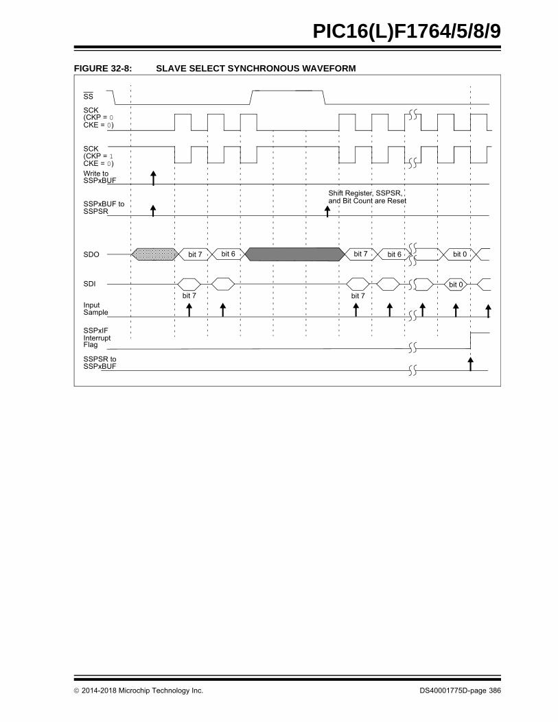
2014-2018 Microchip Technology Inc. DS40001775D-page 386
PIC16(L)F1764/5/8/9
FIGURE 32-8: SLAVE SELECT SYNCHRONOUS WAVEFORM
SCK(CKP = 1
SCK(CKP = 0
InputSample
SDI
bit 7
SDO bit 7 bit 6 bit 7
SSPxIFInterrupt
CKE = 0)
CKE = 0)Write toSSPxBUF
SSPSR toSSPxBUF
SS
Flag
bit 0
bit 7
bit 0
bit 6
SSPxBUF toSSPSR
Shift Register, SSPSR,and Bit Count are Reset

2014-2018 Microchip Technology Inc. DS40001775D-page 387
PIC16(L)F1764/5/8/9
FIGURE 32-9: SPI MODE WAVEFORM (SLAVE MODE WITH CKE = 0)
FIGURE 32-10: SPI MODE WAVEFORM (SLAVE MODE WITH CKE = 1)
SCK(CKP = 1
SCK(CKP = 0
InputSample
SDI
bit 7
SDO bit 7 bit 6 bit 5 bit 4 bit 3 bit 2 bit 1 bit 0
SSPxIFInterrupt
CKE = 0)
CKE = 0)
Write toSSPxBUF Valid
SSPSR toSSPxBUF
SS
Flag
Optional
Detection ActiveWrite Collision
bit 0
SCK(CKP = 1
SCK(CKP = 0
InputSample
SDI
bit 7 bit 0
SDO bit 6 bit 5 bit 4 bit 3 bit 2 bit 1 bit 0
SSPxIFInterrupt
CKE = 1)
CKE = 1)
Write toSSPxBUF Valid
SSPSR toSSPxBUF
SS
Flag
Not Optional
Write CollisionDetection Active
bit 7

2014-2018 Microchip Technology Inc. DS40001775D-page 388
PIC16(L)F1764/5/8/9
32.2.6 SPI OPERATION IN SLEEP MODE
In SPI Master mode, module clocks may be operatingat a different speed than when in Full-Power mode; inthe case of the Sleep mode, all clocks are halted.
Special care must be taken by the user when the MSSPclock is much faster than the system clock.
In Slave mode, when MSSP interrupts are enabled,after the master completes sending data, an MSSPinterrupt will wake the controller from Sleep.
If an exit from Sleep mode is not desired, MSSPinterrupts should be disabled.
In SPI Master mode, when the Sleep mode is selected,all module clocks are halted and the transmis-sion/reception will remain in that state until the devicewakes. After the device returns to Run mode, themodule will resume transmitting and receiving data.
In SPI Slave mode, the SPI Transmit/Receive Shiftregister operates asynchronously to the device. Thisallows the device to be placed in Sleep mode and datato be shifted into the SPI Transmit/Receive Shiftregister. When all eight bits have been received, theMSSP interrupt flag bit will be set and if enabled, willwake the device.
TABLE 32-1: SUMMARY OF REGISTERS ASSOCIATED WITH SPI OPERATION
Name Bit 7 Bit 6 Bit 5 Bit 4 Bit 3 Bit 2 Bit 1 Bit 0Register on Page
ANSELA — — — ANSA4 — ANSA<2:0> 137
ANSELC ANSC<7:6>(2) — — ANSC<3:0> 148
INTCON GIE PEIE TMR0IE INTE IOCIE TMR0IF INTF IOCIF 101
PIE1 TMR1GIE ADIE RCIE TXIE SSP1IE CCP1IE TMR2IE TMR1IE 102
PIR1 TMR1GIF ADIF RCIF TXIF SSP1IF CCP1IF TMR2IF TMR1IF 105
RxyPPS — — — RxyPPS<4:0> 154
SSPCLKPPS — — — SSPCLKPPS<4:0> 154, 156
SSPDATPPS — — — SSPDATPPS<4:0> 154, 156
SSPSSPPS — — — SSPSSPPS<4:0> 154, 156
SSP1BUF Synchronous Serial Port Receive Buffer/Transmit Register 381*
SSP1CON1 WCOL SSPOV SSPEN CKP SSPM<3:0> 427
SSP1CON3 ACKTIM PCIE SCIE BOEN SDAHT SBCDE AHEN DHEN 425
SSP1STAT SMP CKE D/A P S R/W UA BF 425
TRISA — — TRISA<5:4> —(1) TRISA<2:0> 136
TRISB(2) TRISB<7:4> — — — — 142
TRISC TRISC<7:6>(2) TRISC<5:0> 147
Legend: — = unimplemented location, read as ‘0’. Shaded cells are not used by the MSSP in SPI mode.
* Page provides register information.
Note 1: Unimplemented, read as ‘1’.
2: PIC16(L)F1768/9 only.
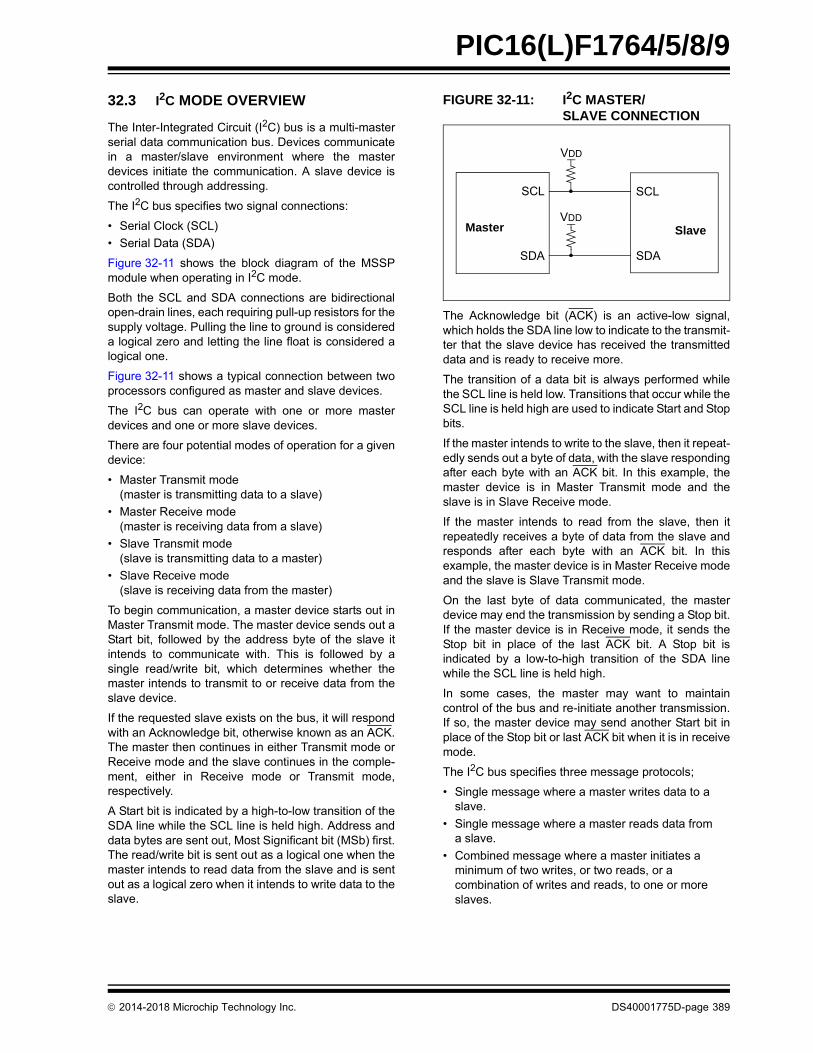
2014-2018 Microchip Technology Inc. DS40001775D-page 389
PIC16(L)F1764/5/8/9
32.3 I2C MODE OVERVIEW
The Inter-Integrated Circuit (I2C) bus is a multi-masterserial data communication bus. Devices communicatein a master/slave environment where the masterdevices initiate the communication. A slave device iscontrolled through addressing.
The I2C bus specifies two signal connections:
• Serial Clock (SCL)
• Serial Data (SDA)
Figure 32-11 shows the block diagram of the MSSPmodule when operating in I2C mode.
Both the SCL and SDA connections are bidirectionalopen-drain lines, each requiring pull-up resistors for thesupply voltage. Pulling the line to ground is considereda logical zero and letting the line float is considered alogical one.
Figure 32-11 shows a typical connection between twoprocessors configured as master and slave devices.
The I2C bus can operate with one or more masterdevices and one or more slave devices.
There are four potential modes of operation for a givendevice:
• Master Transmit mode(master is transmitting data to a slave)
• Master Receive mode(master is receiving data from a slave)
• Slave Transmit mode(slave is transmitting data to a master)
• Slave Receive mode(slave is receiving data from the master)
To begin communication, a master device starts out inMaster Transmit mode. The master device sends out aStart bit, followed by the address byte of the slave itintends to communicate with. This is followed by asingle read/write bit, which determines whether themaster intends to transmit to or receive data from theslave device.
If the requested slave exists on the bus, it will respondwith an Acknowledge bit, otherwise known as an ACK.The master then continues in either Transmit mode orReceive mode and the slave continues in the comple-ment, either in Receive mode or Transmit mode,respectively.
A Start bit is indicated by a high-to-low transition of theSDA line while the SCL line is held high. Address anddata bytes are sent out, Most Significant bit (MSb) first.The read/write bit is sent out as a logical one when themaster intends to read data from the slave and is sentout as a logical zero when it intends to write data to theslave.
FIGURE 32-11: I2C MASTER/SLAVE CONNECTION
The Acknowledge bit (ACK) is an active-low signal,which holds the SDA line low to indicate to the transmit-ter that the slave device has received the transmitteddata and is ready to receive more.
The transition of a data bit is always performed whilethe SCL line is held low. Transitions that occur while theSCL line is held high are used to indicate Start and Stopbits.
If the master intends to write to the slave, then it repeat-edly sends out a byte of data, with the slave respondingafter each byte with an ACK bit. In this example, themaster device is in Master Transmit mode and theslave is in Slave Receive mode.
If the master intends to read from the slave, then itrepeatedly receives a byte of data from the slave andresponds after each byte with an ACK bit. In thisexample, the master device is in Master Receive modeand the slave is Slave Transmit mode.
On the last byte of data communicated, the masterdevice may end the transmission by sending a Stop bit.If the master device is in Receive mode, it sends theStop bit in place of the last ACK bit. A Stop bit isindicated by a low-to-high transition of the SDA linewhile the SCL line is held high.
In some cases, the master may want to maintaincontrol of the bus and re-initiate another transmission.If so, the master device may send another Start bit inplace of the Stop bit or last ACK bit when it is in receivemode.
The I2C bus specifies three message protocols;
• Single message where a master writes data to a slave.
• Single message where a master reads data from a slave.
• Combined message where a master initiates a minimum of two writes, or two reads, or a combination of writes and reads, to one or more slaves.
Master
SCL
SDA
SCL
SDA
SlaveVDD
VDD

2014-2018 Microchip Technology Inc. DS40001775D-page 390
PIC16(L)F1764/5/8/9
When one device is transmitting a logical one, or lettingthe line float, and a second device is transmitting a log-ical zero, or holding the line low, the first device candetect that the line is not a logical one. This detection,when used on the SCL line, is called clock stretching.Clock stretching gives slave devices a mechanism tocontrol the flow of data. When this detection is used onthe SDA line, it is called arbitration. Arbitration ensuresthat there is only one master device communicating atany single time.
32.3.1 CLOCK STRETCHING
When a slave device has not completed processingdata, it can delay the transfer of more data through theprocess of clock stretching. An addressed slave devicemay hold the SCL clock line low after receiving or send-ing a bit, indicating that it is not yet ready to continue.The master that is communicating with the slave willattempt to raise the SCL line in order to transfer thenext bit, but will detect that the clock line has not yetbeen released. Because the SCL connection isopen-drain, the slave has the ability to hold that line lowuntil it is ready to continue communicating.
Clock stretching allows receivers that cannot keep upwith a transmitter to control the flow of incoming data.
32.3.2 ARBITRATION
Each master device must monitor the bus for Start andStop bits. If the device detects that the bus is busy, itcannot begin a new message until the bus returns to anIdle state.
However, two master devices may try to initiate a trans-mission on or about the same time. When this occurs,the process of arbitration begins. Each transmitterchecks the level of the SDA data line and compares itto the level that it expects to find. The first transmitter toobserve that the two levels do not match, losesarbitration and must stop transmitting on the SDA line.
For example, if one transmitter holds the SDA line to alogical one (lets it float) and a second transmitter holdsit to a logical zero (pulls it low), the result is that theSDA line will be low. The first transmitter then observesthat the level of the line is different than expected andconcludes that another transmitter is communicating.
The first transmitter to notice this difference is the onethat loses arbitration and must stop driving the SDAline. If this transmitter is also a master device, it alsomust stop driving the SCL line. It then can monitor thelines for a Stop condition before trying to re-issue itstransmission. In the meantime, the other device thathas not noticed any difference between the expectedand actual levels on the SDA line continues with itsoriginal transmission. It can do so without any compli-cations, because so far, the transmission appearsexactly as expected with no other transmitter disturbingthe message.
Slave Transmit mode can also be arbitrated, when amaster addresses multiple slaves, but this is lesscommon.
If two master devices are sending a message to twodifferent slave devices at the address stage, the mastersending the lower slave address always wins arbitra-tion. When two master devices send messages to thesame slave address, and addresses can sometimesrefer to multiple slaves, the arbitration process mustcontinue into the data stage.
Arbitration usually occurs very rarely, but it is anecessary process for proper multi-master support.

2014-2018 Microchip Technology Inc. DS40001775D-page 391
PIC16(L)F1764/5/8/9
32.4 I2C MODE OPERATION
All MSSP I2C communication is byte-oriented andshifted out, MSb first. Six SFR registers and twointerrupt flags interface the module with the PIC®
microcontroller and user software. Two pins, SDA andSCL, are exercised by the module to communicatewith other external I2C devices.
32.4.1 BYTE FORMAT
All communication in I2C is done in 9-bit segments. Abyte is sent from a master to a slave or vice-versa,followed by an Acknowledge bit sent back. After theeighth falling edge of the SCL line, the device output-ting data on the SDA changes that pin to an input andreads in an Acknowledge value on the next clockpulse.
The clock signal, SCL, is provided by the master. Datais valid to change while the SCL signal is low, andsampled on the rising edge of the clock. Changes onthe SDA line while the SCL line is high define specialconditions on the bus, explained below.
32.4.2 DEFINITION OF I2C TERMINOLOGY
There is language and terminology in the descriptionof I2C communication that have definitions specific toI2C. That word usage is defined below and may beused in the rest of this document without explanation.This table was adapted from the Philips® I2Cspecification.
32.4.3 SDA AND SCL PINS
Selection of any I2C mode with the SSPEN bit set,forces the SCL and SDA pins to be open-drain. Thesepins should be set by the user to inputs by setting theappropriate TRISx bits.
32.4.4 SDA HOLD TIME
The hold time of the SDA pin is selected by the SDAHTbit of the SSPxCON3 register. Hold time is the timeSDA is held valid after the falling edge of SCL. Settingthe SDAHT bit selects a longer 300 ns minimum holdtime and may help on buses with large capacitance.
TABLE 32-2: I2C BUS TERMS
Note 1: Data is tied to output zero when an I2Cmode is enabled.
2: Any device pin can be selected for SDAand SCL functions with the PPS peripheral.These functions are bidirectional. The SDAinput is selected with the SSPDATPPSregisters. The SCL input is selected withthe SSPCLKPPS registers. Outputs areselected with the RxyPPS registers. It is theuser’s responsibility to make the selectionsso that both the input and the output foreach function is on the same pin.
TERM Description
Transmitter The device which shifts data out onto the bus.
Receiver The device which shifts data in from the bus.
Master The device that initiates a transfer, generates clock signals and terminates a transfer.
Slave The device addressed by the master.
Multi-master A bus with more than one device that can initiate data transfers.
Arbitration Procedure to ensure that only one master at a time controls the bus. Winning arbitration ensures that the message is not corrupted.
Synchronization Procedure to synchronize the clocks of two or more devices on the bus.
Idle No master is controlling the bus, and both SDA and SCL lines are high.
Active Any time one or more master devices is controlling the bus.
Addressed Slave
Slave device that has received a matching address and is actively being clocked by a master.
Matching Address
Address byte that is clocked into a slave that matches the value stored in SSPxADD.
Write Request Slave receives a matching address with R/W bit clear and is ready to clock in data.
Read Request Master sends an address byte with the R/W bit set, indicating that it wishes to clock data out of the slave. This data is the next and all following bytes until a Restart or Stop.
Clock Stretching When a device on the bus hold SCL low to stall communication.
Bus Collision Any time the SDA line is sampled low by the module while it is outputting and expected high state.

2014-2018 Microchip Technology Inc. DS40001775D-page 392
PIC16(L)F1764/5/8/9
32.4.5 START CONDITION
The I2C specification defines a Start condition as atransition of SDA from a high to a low state while theSCL line is high. A Start condition is always generatedby the master and signifies the transition of the busfrom an Idle to an active state. Figure 32-12 showswave forms for Start and Stop conditions.
A bus collision can occur on a Start condition if themodule samples the SDA line low before asserting itlow. This does not conform to the I2C specification thatstates no bus collision can occur on a Start.
32.4.6 STOP CONDITION
A Stop condition is a transition of the SDA line fromlow-to-high state while the SCL line is high.
32.4.7 RESTART CONDITION
A Restart is valid any time that a Stop would be valid.A master can issue a Restart if it wishes to hold thebus after terminating the current transfer. A Restarthas the same effect on the slave that a Start would,resetting all slave logic and preparing it to clock in anaddress. The master may want to address the same oranother slave. Figure 32-13 shows the wave form for aRestart condition.
In 10-Bit Addressing Slave mode, a Restart is requiredfor the master to clock data out of the addressedslave. Once a slave has been fully addressed, match-ing both high and low address bytes, the master canissue a Restart and the high address byte with theR/W bit set. The slave logic will then hold the clockand prepare to clock out data.
After a full match with R/W clear in 10-bit mode, a priormatch flag is set and maintained until a Stop condition, ahigh address with R/W clear or high address match fails.
32.4.8 START/STOP CONDITION INTERRUPT MASKING
The SCIE and PCIE bits of the SSPxCON3 registercan enable the generation of an interrupt in Slavemodes that do not typically support this function. InSlave modes where interrupt on Start and Stop detectis already enabled, these bits will have no effect.
FIGURE 32-12: I2C START AND STOP CONDITIONS
FIGURE 32-13: I2C RESTART CONDITION
Note: At least one SCL low time must appearbefore a Stop is valid, therefore, if the SDAline goes low, then high again while the SCLline stays high, only the Start condition isdetected.
SDA
SCL
P
StopCondition
S
StartCondition
Change ofData Allowed
Change ofData Allowed
RestartCondition
Sr
Change ofData Allowed
Change ofData Allowed

2014-2018 Microchip Technology Inc. DS40001775D-page 393
PIC16(L)F1764/5/8/9
32.4.9 ACKNOWLEDGE SEQUENCE
The 9th SCL pulse for any transferred byte in I2C isdedicated as an Acknowledge. It allows receivingdevices to respond back to the transmitter by pullingthe SDA line low. The transmitter must release controlof the line during this time to shift in the response. TheAcknowledge (ACK) is an active-low signal, pulling theSDA line low indicates to the transmitter that thedevice has received the transmitted data and is readyto receive more.
The result of an ACK is placed in the ACKSTAT bit ofthe SSPxCON2 register.
Slave software, when the AHEN and DHEN bits areset, allows the user to set the ACK value sent back tothe transmitter. The ACKDT bit of the SSPxCON2register is set/cleared to determine the response.
Slave hardware will generate an ACK response if theAHEN and DHEN bits of the SSPxCON3 register areclear.
There are certain conditions where an ACK will not besent by the slave. If the BF bit of the SSPxSTAT regis-ter or the SSPOV bit of the SSPxCON1 register areset when a byte is received.
When the module is addressed, after the eighth fallingedge of SCL on the bus, the ACKTIM bit of theSSPxCON3 register is set. The ACKTIM bit indicatesthe Acknowledge time of the active bus. The ACKTIMstatus bit is only active when the AHEN bit or DHEN bitis enabled.
32.5 I2C Slave Mode Operation
The MSSP Slave mode operates in one of four modesselected by the SSPM<3:0> bits of SSPxCON1 regis-ter. The modes can be divided into 7-Bit and 10-BitAddressing modes. 10-Bit Addressing mode operatesthe same as 7-bit with some additional overhead forhandling the larger addresses.
Modes with Start and Stop bit interrupts operate thesame as the other modes, with SSPxIF additionallygetting set upon detection of a Start, Restart or Stopcondition.
32.5.1 SLAVE MODE ADDRESSES
The SSPxADD register (Register 32-6) contains theSlave mode address. The first byte received after aStart or Restart condition is compared against thevalue stored in this register. If the byte matches, thevalue is loaded into the SSPxBUF register and aninterrupt is generated. If the value does not match, themodule goes Idle and no indication is given to thesoftware that anything happened.
The SSP Mask register (Register 32-5) affects theaddress matching process. See Section 32.5.8 “SSPMask Register” for more information.
32.5.1.1 I2C Slave 7-Bit Addressing Mode
In 7-Bit Addressing mode, the LSb of the received databyte is ignored when determining if there is an addressmatch.
32.5.1.2 I2C Slave 10-Bit Addressing Mode
In 10-Bit Addressing mode, the first received byte iscompared to the binary value of ‘1 1 1 1 0 A9 A8 0’.A9 and A8 are the two MSbs of the 10-bit address andstored in bits 2 and 1 of the SSPxADD register.
After the Acknowledge of the high byte, the UA bit isset and SCL is held low until the user updatesSSPxADD with the low address. The low address byteis clocked in and all eight bits are compared to the lowaddress value in SSPxADD. Even if there is not anaddress match, SSPxIF and UA are set, and SCL isheld low until SSPxADD is updated to receive a highbyte again. When SSPxADD is updated, the UA bit iscleared. This ensures the module is ready to receivethe high address byte on the next communication.
A high and low address match as a write request isrequired at the start of all 10-Bit Addressing communi-cation. A transmission can be initiated by issuing aRestart once the slave is addressed, and clocking inthe high address with the R/W bit set. The slavehardware will then Acknowledge the read request andprepare to clock out data. This is only valid for a slaveafter it has received a complete high and low addressbyte match.
2014-2018 Microchip Technology Inc. DS40001775D-page 394
PIC16(L)F1764/5/8/9
32.5.2 SLAVE RECEPTION
When the R/W bit of a matching received address byteis clear, the R/W bit of the SSPxSTAT register iscleared. The received address is loaded into theSSPxBUF register and Acknowledged.
When the overflow condition exists for a receivedaddress, then not Acknowledge is given. An overflowcondition is defined as either bit, BF of the SSPxSTATregister, is set or bit, SSPOV of the SSPxCON1 regis-ter, is set. The BOEN bit of the SSPxCON3 registermodifies this operation. For more information seeRegister 32-4.
An MSSP interrupt is generated for each transferreddata byte. Flag bit, SSPxIF, must be cleared bysoftware.
When the SEN bit of the SSPxCON2 register is set,SCL will be held low (clock stretch) following eachreceived byte. The clock must be released by settingthe CKP bit of the SSPxCON1 register, exceptsometimes in 10-bit mode. See Section 32.5.6.2“10-Bit Addressing Mode” for more detail.
32.5.2.1 7-Bit Addressing Reception
This section describes a standard sequence of eventsfor the MSSP module configured as an I2C slave in7-Bit Addressing mode. Figure 32-14 andFigure 32-15 is used as a visual reference for thisdescription.
This is a step by step process of what typically mustbe done to accomplish I2C communication.
1. Start bit is detected.
2. S bit of SSPxSTAT is set; SSPxIF is set ifinterrupt on Start detect is enabled.
3. Matching address with R/W bit clear is received.
4. The slave pulls SDA low, sending an ACK to themaster and sets the SSPxIF bit.
5. Software clears the SSPxIF bit.
6. Software reads the received address fromSSPxBUF, clearing the BF flag.
7. If SEN = 1, slave software sets the CKP bit torelease the SCL line.
8. The master clocks out a data byte.
9. Slave drives SDA low, sending an ACK to themaster and sets the SSPxIF bit.
10. Software clears SSPxIF.
11. Software reads the received byte fromSSPxBUF, clearing BF.
12. Steps 8-12 are repeated for all received bytesfrom the master.
13. Master sends Stop condition, setting P bit ofSSPxSTAT and the bus goes Idle.
32.5.2.2 7-Bit Reception with AHEN and DHEN
Slave device reception with AHEN and DHEN setoperates the same as without these options with extrainterrupts and clock stretching added after the eighthfalling edge of SCL. These additional interrupts allowthe slave software to decide whether it wants to ACKthe receive address or data byte, rather than the hard-ware. This functionality adds support for PMBus™ thatwas not present on previous versions of this module.
This list describes the steps that need to be taken byslave software to use these options for I2C communi-cation. Figure 32-16 displays a module using bothaddress and data holding. Figure 32-17 includes theoperation with the SEN bit of the SSPxCON2 registerset.
1. S bit of SSPxSTAT is set; SSPxIF is set ifinterrupt on Start detect is enabled.
2. Matching address with R/W bit clear is clockedin. SSPxIF is set and CKP cleared after theeighth falling edge of SCL.
3. Slave clears SSPxIF.
4. Slave can look at the ACKTIM bit of theSSPxCON3 register to determine if SSPxIF wasafter or before the ACK.
5. Slave reads the address value from SSPxBUF,clearing the BF flag.
6. Slave sets ACK value clocked out to the masterby setting ACKDT.
7. Slave releases the clock by setting CKP.
8. SSPxIF is set after an ACK, not after a NACK.
9. If SEN = 1, the slave hardware will stretch theclock after the ACK.
10. Slave clears SSPxIF.
11. SSPxIF is set and CKP cleared after eighthfalling edge of SCL for a received data byte.
12. Slave looks at ACKTIM bit of SSPxCON3 todetermine the source of the interrupt.
13. Slave reads the received data from SSPxBUF,clearing BF.
14. Steps 7-14 are the same for each received databyte.
15. Communication is ended by either the slavesending an ACK = 1 or the master sending aStop condition. If a Stop is sent and interrupt onStop detect is disabled, the slave will only knowby polling the P bit of the SSPxSTAT register.
Note: SSPxIF is still set after the 9th falling edgeof SCL even if there is no clock stretchingand BF has been cleared. Only if NACK issent to master is SSPxIF not set

2014-2018
Microchip T
echnology Inc.D
S40001775D
-page 395
PIC
16(L)F
1764/5/8/9
FIG
UR
E 32-14
:I 2C
SL
AV
E, 7
-BIT
AD
DR
ES
S, R
EC
EP
TIO
N (S
EN
=0
, AH
EN
=0
, DH
EN
=0
)
Receiving Address
ACK
Receiving Data
ACK
Receiving Data ACK = 1
A7 A6 A5 A4 A3 A2 A1 D7 D6 D5 D4 D3 D2 D1 D0 D7 D6 D5 D4 D3 D2 D1 D0SDA
SCL
SSPxIF
BF
SSPOV
1 2 3 4 5 6 7 8 1 2 3 4 5 6 7 8 1 2 3 4 5 6 7 89 9 9
ACK is not sent.
SSPOV set becauseSSPxBUF is still full.
Cleared by software
First byte of data is available in SSPxBUF
SSPxBUF is read
SSPxIF set on 9thfalling edge of SCL
Cleared by software
P
Bus Master sends Stop condition
S
From Slave to Master

2014-2018
Microchip T
echnology Inc.D
S40001775D
-page 396
PIC
16(L)F
1764/5/8/9
FIG
UR
E 32-15
:I 2C
SL
AV
E, 7
-BIT
AD
DR
ES
S, R
EC
EP
TIO
N (S
EN
=1
, AH
EN
=0
, DH
EN
=0
)
SEN SEN
A7 A6 A5 A4 A3 A2 A1 D7 D6 D5 D4 D3 D2 D1 D0 D7 D6 D5 D4 D3 D2 D1 D0SDA
SCL 1 2 3 4 5 6 7 8 9 1 2 3 4 5 6 7 8 9 1 2 3 4 5 6 7 8 9 P
SSPxIF set on 9th
SCL is not heldCKP is written to ‘1’ in software, CKP is written to ‘1’ in software,
ACK
low because
falling edge of SCL
releasing SCL
ACK is not sent.
Bus Master sends
CKP
SSPOV
BF
SSPxIF
SSPOV set becauseSSPxBUF is still full.
Cleared by software
First byte of data is available in SSPxBUF
ACK= 1
Cleared by software
SSPxBUF is read
Clock is held low until CKP is set to ‘1’
releasing SCL
Stop condition
S
ACK
ACKReceive Address Receive Data Receive DataR/W = 0

2014-2018
Microchip T
echnology Inc.D
S40001775D
-page 397
PIC
16(L)F
1764/5/8/9
FIG
UR
E 32-16
:I 2C
SL
AV
E, 7
-BIT
AD
DR
ES
S, R
EC
EP
TIO
N (S
EN
=0
, AH
EN
=1
, DH
EN
=1
)
Receiving Address Receiving Data Received Data
P
A7 A6 A5 A4 A3 A2 A1 D7 D6 D5 D4 D3 D2 D1 D0 D7 D6 D5 D4 D3 D2 D1 D0SDA
SCL
BF
CKP
S
P
1 2 3 4 5 6 7 8 9 1 2 3 4 5 6 7 8 9 1 2 3 4 5 6 7 8
Master sendsStop condition
S
Data is read from SSPxBUF
Cleared by softwareSSPxIF is set on 9th falling edge of SCL, after ACK
CKP set by software, SCL is released
Slave software
9
ACKTIM cleared byhardware in 9th rising edge of SCL
sets ACKDT to
not ACK
When DHEN=1:CKP is cleared byhardware on 8th fallingedge of SCL
Slave softwareclears ACKDT to
ACK the receivedbyte
ACKTIM set by hardwareon 8th falling edge of SCL
When AHEN=1:CKP is cleared by hardwareand SCL is stretched
Address isread from SSBUF
ACKTIM set by hardwareon 8th falling edge of SCL
ACK
Master Releases SDAto slave for ACK sequence
No interruptafter not ACKfrom Slave
ACK=1ACK
ACKDT
ACKTIM
SSPxIF
If AHEN = 1:SSPxIF is set

2014-2018
Microchip T
echnology Inc.D
S40001775D
-page 398
PIC
16(L)F
1764/5/8/9
FIG
UR
E 32-17
:I 2C
SL
AV
E, 7
-BIT
AD
DR
ES
S, R
EC
EP
TIO
N (S
EN
= 1
, AH
EN
=1
, DH
EN
=1
)
Receiving Address Receive Data Receive Data
A7 A6 A5 A4 A3 A2 A1 D7 D6 D5 D4 D3 D2 D1 D0 D7 D6 D5 D4 D3 D2 D1 D0SDA
SCL
SSPxIF
BF
ACKDT
CKP
S
P
ACK
S1 2 3 4 5 6 7 8 9 1 2 3 4 5 6 7 8 9 1 2 3 4 5 6 7 8 9
ACK
ACK
Cleared by software
ACKTIM is cleared by hardware
SSPxBUF can be
Set by software,
read any time beforenext byte is loaded
release SCL
on 9th rising edge of SCL
Received address is loaded into SSPxBUF
Slave software clearsACKDT to ACK
R/W = 0Master releasesSDA to slave for ACK sequence
the received byte
When AHEN = 1;on the 8th falling edgeof SCL of an addressbyte, CKP is cleared
ACKTIM is set by hardwareon 8th falling edge of SCL
When DHEN = 1;on the 8th falling edgeof SCL of a receiveddata byte, CKP is cleared
Received data isavailable on SSPxBUF
Slave sendsnot ACK
CKP is not clearedif not ACK
P
Master sendsStop condition
No interrupt after
if not ACKfrom Slave
ACKTIM

2014-2018 Microchip Technology Inc. DS40001775D-page 399
PIC16(L)F1764/5/8/9
32.5.3 SLAVE TRANSMISSION
When the R/W bit of the incoming address byte is setand an address match occurs, the R/W bit of theSSPxSTAT register is set. The received address isloaded into the SSPxBUF register, and an ACK pulse issent by the slave on the ninth bit.
Following the ACK, slave hardware clears the CKP bitand the SCL pin is held low (see Section 32.5.6“Clock Stretching” for more detail). By stretching theclock, the master will be unable to assert another clockpulse until the slave is done preparing the transmitdata.
The transmit data must be loaded into the SSPxBUFregister which also loads the SSPSR register. Then,the SCL pin should be released by setting the CKP bitof the SSPxCON1 register. The eight data bits areshifted out on the falling edge of the SCL input. Thisensures that the SDA signal is valid during the SCLhigh time.
The ACK pulse from the master-receiver is latched onthe rising edge of the ninth SCL input pulse. This ACKvalue is copied to the ACKSTAT bit of the SSPxCON2register. If ACKSTAT is set (not ACK), then the datatransfer is complete. In this case, when the not ACK islatched by the slave, the slave goes Idle and waits foranother occurrence of the Start bit. If the SDA line waslow (ACK), the next transmit data must be loaded intothe SSPxBUF register. Again, the SCL pin must bereleased by setting bit CKP.
An MSSP interrupt is generated for each data transferbyte. The SSPxIF bit must be cleared by software andthe SSPxSTAT register is used to determine the statusof the byte. The SSPxIF bit is set on the falling edge ofthe ninth clock pulse.
32.5.3.1 Slave Mode Bus Collision
A slave receives a read request and begins shiftingdata out on the SDA line. If a bus collision is detectedand the SBCDE bit of the SSPxCON3 register is set,the BCLIF bit of the PIR register is set. Once a bus col-lision is detected, the slave goes Idle and waits to beaddressed again. User software can use the BCLIF bitto handle a slave bus collision.
32.5.3.2 7-Bit Transmission
A master device can transmit a read request to a slaveand then clock data out of the slave. The list belowoutlines what software for a slave will need to do toaccomplish a standard transmission. Figure 32-18 canbe used as a reference to this list.
1. Master sends a Start condition on SDA andSCL.
2. S bit of SSPxSTAT is set; SSPxIF is set ifinterrupt on Start detect is enabled.
3. Matching address with R/W bit set is received bythe slave, setting SSPxIF bit.
4. Slave hardware generates an ACK and setsSSPxIF.
5. SSPxIF bit is cleared by user.
6. Software reads the received address fromSSPxBUF, clearing BF.
7. R/W is set so CKP was automatically clearedafter the ACK.
8. The slave software loads the transmit data intoSSPxBUF.
9. CKP bit is set, releasing SCL, allowing themaster to clock the data out of the slave.
10. SSPxIF is set after the ACK response from themaster is loaded into the ACKSTAT register.
11. SSPxIF bit is cleared.
12. The slave software checks the ACKSTAT bit tosee if the master wants to clock out more data.
13. Steps 9-13 are repeated for each transmittedbyte.
14. If the master sends a not ACK, the clock is notheld, but SSPxIF is still set.
15. The master sends a Restart condition or a Stop.
16. The slave is no longer addressed.
Note 1: If the master ACKs, the clock will bestretched.
2: ACKSTAT is the only bit updated on therising edge of SCL (9th), rather than thefalling.
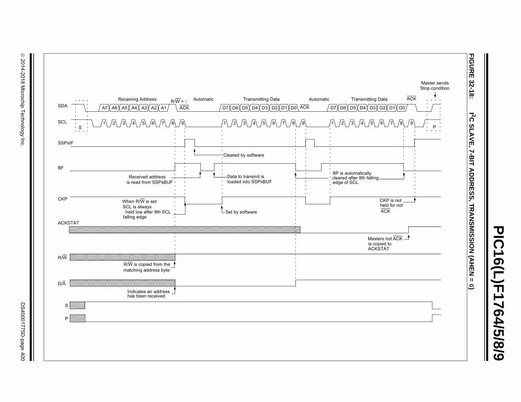
2014-2018
Microchip T
echnology Inc.D
S40001775D
-page 400
PIC
16(L)F
1764/5/8/9
FIG
UR
E 32-18
:I 2C
SL
AV
E, 7
-BIT
AD
DR
ES
S, T
RA
NS
MIS
SIO
N (A
HE
N=
0)
Receiving Address Automatic Transmitting Data Automatic Transmitting Data
A7 A6 A5 A4 A3 A2 A1 D7 D6 D5 D4 D3 D2 D1 D0 D7 D6 D5 D4 D3 D2 D1 D0
1 2 3 4 5 6 7 8 9 1 2 3 4 5 6 7 8 9 1 2 3 4 5 6 7 8 9
SDA
SCL
SSPxIF
BF
CKP
ACKSTAT
R/W
D/A
S
P
Received address
When R/W is set
R/W is copied from the
Indicates an address
is read from SSPxBUF
SCL is alwaysheld low after 9th SCL
falling edge
matching address byte
has been received
Masters not ACKis copied to ACKSTAT
CKP is not held for not ACK
BF is automatically cleared after 8th fallingedge of SCL
Data to transmit isloaded into SSPxBUF
Set by software
Cleared by software
ACKACK
ACKR/W = 1
S P
Master sendsStop condition

2014-2018 Microchip Technology Inc. DS40001775D-page 401
PIC16(L)F1764/5/8/9
32.5.3.3 7-Bit Transmission with Address Hold Enabled
Setting the AHEN bit of the SSPxCON3 registerenables additional clock stretching and interruptgeneration after the eighth falling edge of a receivedmatching address. Once a matching address hasbeen clocked in, CKP is cleared and the SSPxIFinterrupt is set.
Figure 32-19 displays a standard waveform of a 7-bitaddress slave transmission with AHEN enabled.
1. Bus starts Idle.
2. Master sends Start condition; the S bit ofSSPxSTAT is set; SSPxIF is set if interrupt onStart detect is enabled.
3. Master sends matching address with R/W bitset. After the eighth falling edge of the SCL line,the CKP bit is cleared and the SSPxIF interruptis generated.
4. Slave software clears SSPxIF.
5. Slave software reads the ACKTIM bit ofSSPxCON3, and R/W and D/A of theSSPxSTAT register to determine the source ofthe interrupt.
6. Slave reads the address value from theSSPxBUF register, clearing the BF bit.
7. Slave software decides from this information if itwishes to ACK or not ACK and sets the ACKDTbit of the SSPxCON2 register accordingly.
8. Slave sets the CKP bit, releasing SCL.
9. Master clocks in the ACK value from the slave.
10. Slave hardware automatically clears the CKP bitand sets SSPxIF after the ACK if the R/W bit isset.
11. Slave software clears SSPxIF.
12. Slave loads value to transmit to the master intoSSPxBUF, setting the BF bit.
13. Slave sets the CKP bit, releasing the clock.
14. Master clocks out the data from the slave andsends an ACK value on the 9th SCL pulse.
15. Slave hardware copies the ACK value into theACKSTAT bit of the SSPxCON2 register.
16. Steps 10-15 are repeated for each bytetransmitted to the master from the slave.
17. If the master sends a not ACK, the slavereleases the bus allowing the master to send aStop and end the communication.
Note: SSPxBUF cannot be loaded until after theACK.
Note: Master must send a not ACK on the lastbyte to ensure that the slave releases theSCL line to receive a Stop.
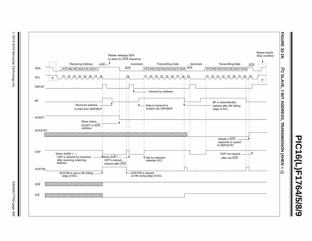
2014-2018
Microchip T
echnology Inc.D
S40001775D
-page 402
PIC
16(L)F
1764/5/8/9
FIG
UR
E 32-19
:I 2C
SL
AV
E, 7
-BIT
AD
DR
ES
S, T
RA
NS
MIS
SIO
N (A
HE
N=
1)
Receiving Address Automatic Transmitting Data Automatic Transmitting Data
A7 A6 A5 A4 A3 A2 A1 D7 D6 D5 D4 D3 D2 D1 D0 D7 D6 D5 D4 D3 D2 D1 D0
1 2 3 4 5 6 7 8 9 1 2 3 4 5 6 7 8 9 1 2 3 4 5 6 7 8 9
SDA
SCL
SSPxIF
BF
ACKDT
ACKSTAT
CKP
R/W
D/A
Received address
is read from SSPxBUF
BF is automatically cleared after 8th fallingedge of SCL
Data to transmit isloaded into SSPxBUF
Cleared by software
Slave clears
ACKDT to ACKaddress
Master’s ACKresponse is copied
to SSPxSTAT
CKP not cleared
after not ACKSet by software,releases SCL
ACKTIM is clearedon 9th rising edge of SCL
ACKTIM is set on 8th fallingedge of SCL
When AHEN = 1;CKP is cleared by hardwareafter receiving matchingaddress.
When R/W = 1;CKP is alwayscleared after ACK
SP
Master sendsStop condition
ACKR/W = 1
Master releases SDAto slave for ACK sequence
ACKACK
ACKTIM

2014-2018 Microchip Technology Inc. DS40001775D-page 403
PIC16(L)F1764/5/8/9
32.5.4 SLAVE MODE 10-BIT ADDRESS RECEPTION
This section describes a standard sequence of eventsfor the MSSP module configured as an I2C slave in10-Bit Addressing mode.
Figure 32-20 is used as a visual reference for thisdescription.
This is a step by step process of what must be done byslave software to accomplish I2C communication.
1. Bus starts Idle.
2. Master sends Start condition. S bit of SSPxSTATis set; SSPxIF is set if interrupt on Start detect isenabled.
3. Master sends matching high address with R/Wbit clear; UA bit of the SSPxSTAT register is set.
4. Slave sends ACK and SSPxIF is set.
5. Software clears the SSPxIF bit.
6. Software reads received address fromSSPxBUF, clearing the BF flag.
7. Slave loads low address into SSPxADD,releasing SCL.
8. Master sends matching low address byte to theslave; UA bit is set.
9. Slave sends ACK and SSPxIF is set.
10. Slave clears SSPxIF.
11. Slave reads the received matching addressfrom SSPxBUF, clearing BF.
12. Slave loads high address into SSPxADD.
13. Master clocks a data byte to the slave andclocks out the slave’s ACK on the 9th SCLpulse; SSPxIF is set.
14. If SEN bit of SSPxCON2 is set, CKP is clearedby hardware and the clock is stretched.
15. Slave clears SSPxIF.
16. Slave reads the received byte from SSPxBUF,clearing BF.
17. If SEN is set, the slave sets CKP to release theSCL.
18. Steps 13-17 repeat for each received byte.
19. Master sends Stop to end the transmission.
32.5.5 10-BIT ADDRESSING WITH ADDRESS OR DATA HOLD
Reception using 10-Bit Addressing with AHEN orDHEN set is the same as with 7-bit modes. The onlydifference is the need to update the SSPxADD registerusing the UA bit. All functionality, specifically when theCKP bit is cleared and the SCL line is held low, are thesame. Figure 32-21 can be used as a reference of aslave in 10-Bit Addressing with AHEN set.
Figure 32-22 shows a standard waveform for a slavetransmitter in 10-Bit Addressing mode.
Note: Updates to the SSPxADD register are notallowed until after the ACK sequence.
Note: If the low address does not match, SSPxIFand UA are still set so that the slave soft-ware can set SSPxADD back to the highaddress. BF is not set because there is nomatch. CKP is unaffected.

2014-2018
Microchip T
echnology Inc.D
S40001775D
-page 404
PIC
16(L)F
1764/5/8/9
FIG
UR
E 32-20
:I 2C
SL
AV
E, 1
0-BIT
AD
DR
ES
S, R
EC
EP
TIO
N (S
EN
=1
, AH
EN
=0
, DH
EN
=0
)
SSPxIF
Receive First Address Byte
ACK
Receive Second Address Byte
ACK
Receive Data
ACK
Receive Data
ACK1 1 1 1 0 A9 A8 A7 A6 A5 A4 A3 A2 A1 A0 D7 D6 D5 D4 D3 D2 D1 D0 D7 D6 D5 D4 D3 D2 D1 D0SDA
SCL
UA
CKP
1 2 3 4 5 6 7 8 9 1 2 3 4 5 6 7 8 9 1 2 3 4 5 6 7 8 9 1 2 3 4 5 6 7 8 9 P
Master sendsStop condition
Cleared by software
Receive address is
Software updates SSPxADD
Data is read
SCL is held low
Set by software,
while CKP = 0
from SSPxBUF
releasing SCLWhen SEN = 1;CKP is cleared after9th falling edge of received byte
read from SSPxBUF
and releases SCLWhen UA = 1;
If address matches
Set by hardwareon 9th falling edge
SSPxADD it is loaded into SSPxBUF
SCL is held low
S
BF

2014-2018
Microchip T
echnology Inc.D
S40001775D
-page 405
PIC
16(L)F
1764/5/8/9
FIG
UR
E 32-21
:I 2C
SL
AV
E, 1
0-BIT
AD
DR
ES
S, R
EC
EP
TIO
N (S
EN
=0
, AH
EN
=1
, DH
EN
=0
)
Receive First Address Byte
UA
Receive Second Address Byte
UA
Receive Data
ACK
Receive Data
1 1 1 1 0 A9 A8 A7 A6 A5 A4 A3 A2 A1 A0 D7 D6 D5 D4 D3 D2 D1 D0 D7 D6 D5SDA
SCL
SSPxIF
BF
ACKDT
UA
CKP
ACKTIM
1 2 3 4 5 6 7 8 9S
ACKACK
1 2 3 4 5 6 7 8 9 1 2 3 4 5 6 7 8 9 1 2
SSPxBUFis read from Received dataSSPxBUF can be
read anytime beforethe next received byte
Cleared by software
falling edge of SCLnot allowed until 9thUpdate to SSPxADD is
Set CKP with software releases SCL
SCLclears UA and releasesUpdate of SSPxADD,
Set by hardwareon 9th falling edge
Slave software clearsACKDT to ACKthe received byte
If when AHEN = 1;on the 8th falling edgeof SCL of an addressbyte, CKP is cleared
ACKTIM is set by hardwareon 8th falling edge of SCL
Cleared by software
R/W = 0
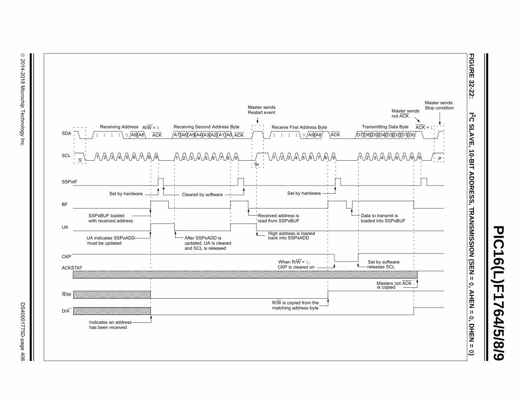
2014-2018
Microchip T
echnology Inc.D
S40001775D
-page 406
PIC
16(L)F
1764/5/8/9
FIG
UR
E 32-22
:I 2C
SL
AV
E, 1
0-BIT
AD
DR
ES
S, TR
AN
SM
ISS
ION
(SE
N=
0, A
HE
N=
0, D
HE
N=
0)
Receiving Address
ACK
Receiving Second Address Byte
Sr
Receive First Address Byte
ACK
Transmitting Data Byte
1 1 1 1 0 A9 A8 A7 A6 A5 A4 A3 A2 A1 A0 1 1 1 1 0 A9 A8 D7 D6 D5 D4 D3 D2 D1 D0SDA
SCL
SSPxIF
BF
UA
CKP
R/W
D/A
1 2 3 4 5 6 7 8 9 1 2 3 4 5 6 7 8 9 1 2 3 4 5 6 7 8 9 1 2 3 4 5 6 7 8 9
ACK = 1
P
Master sends Stop condition
Master sends not ACK
Master sends Restart event
ACK
R/W = 0
S
Cleared by software
After SSPxADD isupdated, UA is clearedand SCL is released
High address is loaded
Received address is Data to transmit is
Set by software
Indicates an address
When R/W = 1;
R/W is copied from the
Set by hardware
UA indicates SSPxADD
SSPxBUF loadedwith received address
must be updated
has been received
loaded into SSPxBUF
releases SCL
Masters not ACKis copied
matching address byte
CKP is cleared on9th falling edge of SCL
read from SSPxBUF
back into SSPxADD
ACKSTAT
Set by hardware

2014-2018 Microchip Technology Inc. DS40001775D-page 407
PIC16(L)F1764/5/8/9
32.5.6 CLOCK STRETCHING
Clock stretching occurs when a device on the busholds the SCL line low, effectively pausing communi-cation. The slave may stretch the clock to allow moretime to handle data or prepare a response for themaster device. A master device is not concerned withstretching, as anytime it is active on the bus and nottransferring data, it is stretching. Any stretching doneby a slave is invisible to the master software andhandled by the hardware that generates SCL.
The CKP bit of the SSPxCON1 register is used tocontrol stretching in software. Any time the CKP bit iscleared, the module will wait for the SCL line to go lowand then hold it. Setting CKP will release SCL andallow more communication.
32.5.6.1 Normal Clock Stretching
Following an ACK, if the R/W bit of SSPxSTAT is setand there is a read request, the slave hardware willclear CKP. This allows the slave time to updateSSPxBUF with data to transfer to the master. If theSEN bit of SSPxCON2 is set, the slave hardware willalways stretch the clock after the ACK sequence.Once the slave is ready, CKP is set by software andcommunication resumes.
32.5.6.2 10-Bit Addressing Mode
In 10-Bit Addressing mode when the UA bit is set, theclock is always stretched. This is the only time the SCLis stretched without CKP being cleared. SCL isreleased immediately after a write to SSPxADD.
32.5.6.3 Byte NACKing
When the AHEN bit of SSPxCON3 is set, CKP iscleared by hardware after the eighth falling edge ofSCL for a received matching address byte. When theDHEN bit of SSPxCON3 is set, CKP is cleared afterthe eighth falling edge of SCL for received data.
Stretching after the eighth falling edge of SCL allowsthe slave to look at the received address or data anddecide if it wants to ACK the received data.
32.5.6.4 Clock Synchronization and the CKP Bit
Any time the CKP bit is cleared, the module will waitfor the SCL line to go low and then hold it. However,clearing the CKP bit will not assert the SCL output lowuntil the SCL output is already sampled low. There-fore, the CKP bit will not assert the SCL line until anexternal I2C master device has already asserted theSCL line. The SCL output will remain low until the CKPbit is set and all other devices on the I2C bus havereleased SCL. This ensures that a write to the CKP bitwill not violate the minimum high time requirement forSCL (see Figure 32-23).
FIGURE 32-23: CLOCK SYNCHRONIZATION TIMING
Note 1: The BF bit has no effect on if the clock willbe stretched or not. This is different thanprevious versions of the module thatwould not stretch the clock, and clearedCKP if SSPxBUF was read before the 9thfalling edge of SCL.
2: Previous versions of the module did notstretch the clock for a transmission ifSSPxBUF was loaded before the 9thfalling edge of SCL; it is now alwayscleared for read requests.
Note: Previous versions of the module did notstretch the clock if the second address bytedid not match.
SDA
SCL
DX – 1DX
WR
Q1 Q2 Q3 Q4 Q1 Q2 Q3 Q4 Q1 Q2 Q3 Q4 Q1 Q2 Q3 Q4 Q1 Q2 Q3 Q4 Q1 Q2 Q3 Q4 Q1 Q2 Q3 Q4
CKP
Master DeviceReleases Clock
Master DeviceAsserts Clock
SSPxCON1

2014-2018 Microchip Technology Inc. DS40001775D-page 408
PIC16(L)F1764/5/8/9
32.5.7 GENERAL CALL ADDRESS SUPPORT
The addressing procedure for the I2C bus is such thatthe first byte after the Start condition usually deter-mines which device will be the slave addressed by themaster device. The exception is the general calladdress which can address all devices. When thisaddress is used, all devices should, in theory, respondwith an Acknowledge.
The general call address is a reserved address in theI2C protocol, defined as address: 0x00. When theGCEN bit of the SSPxCON2 register is set, the slavemodule will automatically ACK the reception of thisaddress, regardless of the value stored in SSPxADD.After the slave clocks in an address of all zeros, with the
R/W bit clear, an interrupt is generated and slave soft-ware can read SSPxBUF and respond. Figure 32-24shows a general call reception sequence.
In 10-Bit Address mode, the UA bit will not be set onthe reception of the general call address. The slavewill prepare to receive the second byte as data, just asit would in 7-bit mode.
If the AHEN bit of the SSPxCON3 register is set, justas with any other address reception, the slave hard-ware will stretch the clock after the eighth falling edgeof SCL. The slave must then set its ACKDT value andrelease the clock with communication progressing as itwould normally.
FIGURE 32-24: SLAVE MODE GENERAL CALL ADDRESS SEQUENCE
32.5.8 SSP MASK REGISTER
An MSSP Mask (SSPxMSK) register (Register 32-5) isavailable in I2C Slave mode as a mask for the valueheld in the SSPSR register during an addresscomparison operation. A zero (‘0’) bit in the SSPxMSKregister has the effect of making the corresponding bitof the received address a “don’t care”.
This register is reset to all ‘1’s upon any Resetcondition, and therefore, has no effect on standardSSP operation until written with a mask value.
The MSSP Mask register is active during:
• 7-Bit Address mode: Address compare of A<7:1>.
• 10-Bit Address mode: Address compare of A<7:0> only. The MSSP mask has no effect during the reception of the first (high) byte of the address.
SDA
SCLS
SSPxIF
BF (SSPxSTAT<0>)
Cleared by Software
SSPxBUF is Read
R/W = 0
ACKGeneral Call Address
Address is Compared to General Call Address
Receiving Data ACK
1 2 3 4 5 6 7 8 9 1 2 3 4 5 6 7 8 9
D7 D6 D5 D4 D3 D2 D1 D0
after ACK, Set Interrupt
GCEN (SSPxCON2<7>)
‘1’

2014-2018 Microchip Technology Inc. DS40001775D-page 409
PIC16(L)F1764/5/8/9
32.6 I2C Master Mode
Master mode is enabled by setting and clearing theappropriate SSPM<3:0> bits in the SSPxCON1 registerand by setting the SSPEN bit. In Master mode, the SDAand SCK pins must be configured as inputs. The MSSPperipheral hardware will override the output driver TRIScontrols when necessary to drive the pins low.
Master mode of operation is supported by interruptgeneration on the detection of the Start and Stopconditions. The Stop (P) and Start (S) bits are clearedfrom a Reset or when the MSSP module is disabled.Control of the I2C bus may be taken when the P bit isset or the bus is Idle.
In Firmware Controlled Master mode, user codeconducts all I2C bus operations based on Start andStop bit condition detection. Start and Stop conditiondetection is the only active circuitry in this mode. Allother communication is done by the user softwaredirectly manipulating the SDA and SCL lines.
The following events will cause the SSP Interrupt Flagbit, SSPxIF, to be set (SSP interrupt, if enabled):
• Start condition detected• Stop condition detected• Data transfer byte transmitted/received• Acknowledge transmitted/received• Repeated Start generated
32.6.1 I2C MASTER MODE OPERATION
The master device generates all of the serial clockpulses, and the Start and Stop conditions. A transferis ended with a Stop condition or with a Repeated Startcondition. Since the Repeated Start condition is alsothe beginning of the next serial transfer, the I2C bus willnot be released.
In Master Transmitter mode, serial data is outputthrough SDA, while SCL outputs the serial clock. Thefirst byte transmitted contains the slave address of thereceiving device (7 bits) and the Read/Write (R/W) bit.In this case, the R/W bit will be logic ‘0’. Serial data istransmitted, eight bits at a time. After each byte istransmitted, an Acknowledge bit is received. Start andStop conditions are output to indicate the beginningand the end of a serial transfer.
In Master Receive mode, the first byte transmittedcontains the slave address of the transmitting device(7 bits) and the R/W bit. In this case, the R/W bit will belogic ‘1’. Thus, the first byte transmitted is a 7-bit slaveaddress followed by a ‘1’ to indicate the receive bit.Serial data is received via SDA, while SCL outputs theserial clock. Serial data is received eight bits at a time.After each byte is received, an Acknowledge bit istransmitted. Start and Stop conditions indicate thebeginning and end of transmission.
A Baud Rate Generator is used to set the clockfrequency output on SCL. See Section 32.7 “BaudRate Generator” for more detail.Note 1: The MSSP module, when configured in
I2C Master mode, does not allow queuingof events. For instance, the user is notallowed to initiate a Start condition andimmediately write the SSPxBUF registerto initiate transmission before the Startcondition is complete. In this case, theSSPxBUF will not be written to and theWCOL bit will be set, indicating that awrite to the SSPxBUF did not occur
2: Master mode suspends Start/Stopdetection when sending the Start/Stopcondition by means of the SEN/PENcontrol bits. The SSPxIF bit is set at theend of the Start/Stop generation whenhardware clears the control bit.

2014-2018 Microchip Technology Inc. DS40001775D-page 410
PIC16(L)F1764/5/8/9
32.6.2 CLOCK ARBITRATION
Clock arbitration occurs when the master, during anyreceive, transmit or Repeated Start/Stop condition,releases the SCL pin (SCL allowed to float high). Whenthe SCL pin is allowed to float high, the Baud RateGenerator (BRG) is suspended from counting until the
SCL pin is actually sampled high. When the SCL pin issampled high, the Baud Rate Generator is reloadedwith the contents of SSPxADD<7:0> and begins count-ing. This ensures that the SCL high time will always beat least one BRG rollover count in the event that theclock is held low by an external device (Figure 32-25).
FIGURE 32-25: BAUD RATE GENERATOR TIMING WITH CLOCK ARBITRATION
32.6.3 WCOL STATUS FLAG
If the user writes the SSPxBUF when a Start, Restart,Stop, receive or transmit sequence is in progress, theWCOL is set and the contents of the buffer areunchanged (the write does not occur). Any time theWCOL bit is set, it indicates that an action on SSPxBUFwas attempted while the module was not Idle.
SDA
SCL
SCL Deasserted but Slave Holds
DX – 1DX
BRG
SCL is Sampled High, Reload TakesPlace and BRG Starts its Count
03h 02h 01h 00h (hold off) 03h 02h
Reload
BRGValue
SCL Low (clock arbitration)SCL Allowed to Transition High
BRG Decrements onQ2 and Q4 Cycles
Note: Because queuing of events is not allowed,writing to the lower five bits of SSPxCON2is disabled until the Start condition iscomplete.

2014-2018 Microchip Technology Inc. DS40001775D-page 411
PIC16(L)F1764/5/8/9
32.6.4 I2C MASTER MODE START CONDITION TIMING
To initiate a Start condition (Figure 32-26), the usersets the Start Enable bit, SEN, of the SSPxCON2 reg-ister. If the SDA and SCL pins are sampled high, theBaud Rate Generator is reloaded with the contents ofSSPxADD<7:0> and starts its count. If SCL and SDAare both sampled high when the Baud Rate Generatortimes out (TBRG), the SDA pin is driven low. The actionof the SDA being driven low while SCL is high is theStart condition and causes the S bit of the SSPxSTATregister to be set. Following this, the Baud RateGenerator is reloaded with the contents ofSSPxADD<7:0> and resumes its count. When theBaud Rate Generator times out (TBRG), the SEN bit ofthe SSPxCON2 register will be automatically cleared
by hardware; the Baud Rate Generator is suspended,leaving the SDA line held low and the Start condition iscomplete.
FIGURE 32-26: FIRST START BIT TIMING
Note 1: If, at the beginning of the Start condition,the SDA and SCL pins are alreadysampled low, or if during the Start condi-tion, the SCL line is sampled low beforethe SDA line is driven low, a bus collisionoccurs. The Bus Collision Interrupt Flag,BCLIF, is set, the Start condition isaborted and the I2C module is reset intoits Idle state.
2: The Philips I2C specification states that abus collision cannot occur on a Start.
SDA
SCLS
TBRG
1st bit 2nd bit
TBRG
SDA = 1,At Completion of Start bit,
SCL = 1
Write to SSPxBUF Occurs HereTBRG
Hardware Clears SEN bit
TBRG
Write to SEN bit Occurs Here Set S bit (SSPxSTAT<3>)
and Sets SSPxIF bit

2014-2018 Microchip Technology Inc. DS40001775D-page 412
PIC16(L)F1764/5/8/9
32.6.5 I2C MASTER MODE REPEATED START CONDITION TIMING
A Repeated Start condition (Figure 32-27) occurs whenthe RSEN bit of the SSPxCON2 register isprogrammed high and the master state machine is nolonger active. When the RSEN bit is set, the SCL pin isasserted low. When the SCL pin is sampled low, theBaud Rate Generator is loaded and begins counting.The SDA pin is released (brought high) for one BaudRate Generator count (TBRG). When the Baud RateGenerator times out, if SDA is sampled high, the SCLpin will be deasserted (brought high). When SCL issampled high, the Baud Rate Generator is reloadedand begins counting. SDA and SCL must be sampledhigh for one TBRG. This action is then followed byassertion of the SDA pin (SDA = 0) for one TBRG whileSCL is high. SCL is asserted low. Following this, theRSEN bit of the SSPxCON2 register will be automati-
cally cleared and the Baud Rate Generator will not bereloaded, leaving the SDA pin held low. As soon as aStart condition is detected on the SDA and SCL pins,the S bit of the SSPxSTAT register will be set. TheSSPxIF bit will not be set until the Baud Rate Generatorhas timed out.
FIGURE 32-27: REPEATED START CONDITION WAVEFORM
Note 1: If RSEN is programmed while any otherevent is in progress, it will not take effect.
2: A bus collision during the Repeated Startcondition occurs if:
• SDA is sampled low when SCL goes from low-to-high.
• SCL goes low before SDA is asserted low. This may indicate that another master is attempting to transmit a data ‘1’.
SDA
SCL
Repeated Start
Write to SSPxCON2
Write to SSPxBUF Occurs Here
At Completion of Start bit,Hardware Clears RSEN bit
1st bit
S bit Set by Hardware
TBRG
TBRG
SDA = 1, SDA = 1, SCL (no change) SCL = 1
Occurs Here
TBRG TBRG TBRG
and Sets SSPxIF
Sr

2014-2018 Microchip Technology Inc. DS40001775D-page 413
PIC16(L)F1764/5/8/9
32.6.6 I2C MASTER MODE TRANSMISSION
Transmission of a data byte, a 7-bit address or theother half of a 10-bit address is accomplished by simplywriting a value to the SSPxBUF register. This action willset the Buffer Full flag bit, BF, and allow the Baud RateGenerator to begin counting and start the next trans-mission. Each bit of address/data will be shifted outonto the SDA pin after the falling edge of SCL isasserted. SCL is held low for one Baud Rate Generatorrollover count (TBRG). Data should be valid before SCLis released high. When the SCL pin is released high, itis held that way for TBRG. The data on the SDA pinmust remain stable for that duration and some holdtime after the next falling edge of SCL. After the eighthbit is shifted out (the falling edge of the eighth clock),the BF flag is cleared and the master releases SDA.This allows the slave device being addressed torespond with an ACK bit during the ninth bit time if anaddress match occurred or if data was received prop-erly. The status of ACK is written into the ACKSTAT biton the rising edge of the ninth clock. If the masterreceives an Acknowledge, the Acknowledge status bit,ACKSTAT, is cleared. If not, the bit is set. After the ninthclock, the SSPxIF bit is set and the master clock (BaudRate Generator) is suspended until the next data byteis loaded into the SSPxBUF, leaving SCL low and SDAunchanged (Figure 32-28).
After the write to the SSPxBUF, each bit of the addresswill be shifted out on the falling edge of SCL until allseven address bits and the R/W bit are completed. Onthe falling edge of the eighth clock, the master willrelease the SDA pin, allowing the slave to respond withan Acknowledge. On the falling edge of the ninth clock,the master will sample the SDA pin to see if the addresswas recognized by a slave. The status of the ACK bit isloaded into the ACKSTAT status bit of the SSPxCON2register. Following the falling edge of the ninth clocktransmission of the address, the SSPxIF is set, the BFflag is cleared and the Baud Rate Generator is turnedoff until another write to the SSPxBUF takes place,holding SCL low and allowing SDA to float.
32.6.6.1 BF Status Flag
In Transmit mode, the BF bit of the SSPxSTAT registeris set when the CPU writes to SSPxBUF and is clearedwhen all eight bits are shifted out.
32.6.6.2 WCOL Status Flag
If the user writes the SSPxBUF when a transmit isalready in progress (i.e., SSPSR is still shifting out adata byte), the WCOL bit is set and the contents of thebuffer are unchanged (the write does not occur).
WCOL must be cleared by software before the nexttransmission.
32.6.6.3 ACKSTAT Status Flag
In Transmit mode, the ACKSTAT bit of the SSPxCON2register is cleared when the slave has sent anAcknowledge (ACK = 0) and is set when the slave doesnot Acknowledge (ACK = 1). A slave sends anAcknowledge when it has recognized its address(including a general call) or when the slave hasproperly received its data.
32.6.6.4 Typical Transmit Sequence:
1. The user generates a Start condition by settingthe SEN bit of the SSPxCON2 register.
2. SSPxIF is set by hardware on completion of theStart.
3. SSPxIF is cleared by software.
4. The MSSP module will wait the required starttime before any other operation takes place.
5. The user loads the SSPxBUF with the slaveaddress to transmit.
6. Address is shifted out the SDA pin until all eightbits are transmitted. Transmission begins assoon as SSPxBUF is written to.
7. The MSSP module shifts in the ACK bit from theslave device and writes its value into theACKSTAT bit of the SSPxCON2 register.
8. The MSSP module generates an interrupt at theend of the ninth clock cycle by setting theSSPxIF bit.
9. The user loads the SSPxBUF with eight bits ofdata.
10. Data is shifted out the SDA pin until all eight bitsare transmitted.
11. The MSSP module shifts in the ACK bit from theslave device and writes its value into theACKSTAT bit of the SSPxCON2 register.
12. Steps 8-11 are repeated for all transmitted databytes.
13. The user generates a Stop or Restart conditionby setting the PEN or RSEN bits of theSSPxCON2 register. Interrupt is generated oncethe Stop/Restart condition is complete.

2014-2018
Microchip T
echnology Inc.D
S40001775D
-page 414
PIC
16(L)F
1764/5/8/9
FIG
UR
E 32-28
:I 2C
MA
ST
ER
MO
DE
WA
VE
FO
RM
(TRA
NS
MIS
SIO
N, 7 O
R 10-B
IT A
DD
RE
SS
)
SDA
SCL
SSPxIF
BF (SSPxSTAT<0>)
SEN
A7 A6 A5 A4 A3 A2 A1 ACK = 0 D7 D6 D5 D4 D3 D2 D1 D0
ACKTransmitting Data or Second Half
R/W = 0Transmit Address to Slave
1 2 3 4 5 6 7 8 9 1 2 3 4 5 6 7 8 9P
Cleared by software service routine
SSPxBUF is written by software
from SSP interrupt
After Start condition, SEN cleared by hardware
S
SSPxBUF written with 7-bit address and R/Wstart transmit
SCL held lowwhile CPU
responds to SSPxIF
SEN = 0
of 10-bit Address
Write SSPxCON2<0> SEN = 1Start condition begins
From slave, clear ACKSTAT bit SSPxCON2<6>
ACKSTAT in SSPxCON2 = 1
Cleared by software
SSPxBUF written
PEN
R/W
Cleared by software

2014-2018 Microchip Technology Inc. DS40001775D-page 415
PIC16(L)F1764/5/8/9
32.6.7 I2C MASTER MODE RECEPTION
Master mode reception (Figure 32-29) is enabled byprogramming the Receive Enable bit, RCEN bit of theSSPxCON2 register.
The Baud Rate Generator begins counting and on eachrollover, the state of the SCL pin changes(high-to-low/low-to-high), and data is shifted into theSSPSR. After the falling edge of the eighth clock, thereceive enable flag is automatically cleared, thecontents of the SSPSR are loaded into the SSPxBUF,the BF flag bit is set, the SSPxIF flag bit is set and theBaud Rate Generator is suspended from counting,holding SCL low. The MSSP is now in Idle stateawaiting the next command. When the buffer is read bythe CPU, the BF flag bit is automatically cleared. Theuser can then send an Acknowledge bit at the end ofreception by setting the Acknowledge SequenceEnable bit, ACKEN, of the SSPxCON2 register.
32.6.7.1 BF Status Flag
In receive operation, the BF bit is set when an addressor data byte is loaded into SSPxBUF from SSPSR. It iscleared when the SSPxBUF register is read.
32.6.7.2 SSPOV Status Flag
In receive operation, the SSPOV bit is set when eightbits are received into the SSPSR and the BF flag bit isalready set from a previous reception.
32.6.7.3 WCOL Status Flag
If the user writes the SSPxBUF when a receive isalready in progress (i.e., SSPSR is still shifting in a databyte), the WCOL bit is set and the contents of the bufferare unchanged (the write does not occur).
32.6.7.4 Typical Receive Sequence:
1. The user generates a Start condition by settingthe SEN bit of the SSPxCON2 register.
2. SSPxIF is set by hardware on completion of theStart.
3. SSPxIF is cleared by software.
4. User writes SSPxBUF with the slave address totransmit and the R/W bit set.
5. Address is shifted out the SDA pin until all eightbits are transmitted. Transmission begins assoon as SSPxBUF is written to.
6. The MSSP module shifts in the ACK bit from theslave device and writes its value into theACKSTAT bit of the SSPxCON2 register.
7. The MSSP module generates an interrupt at theend of the ninth clock cycle by setting theSSPxIF bit.
8. User sets the RCEN bit of the SSPxCON2 regis-ter and the master clocks in a byte from the slave.
9. After the eighth falling edge of SCL, SSPxIF andBF are set.
10. Master clears SSPxIF and reads the receivedbyte from SSPxBUF, clears BF.
11. Master sets ACK value sent to slave in ACKDTbit of the SSPxCON2 register and initiates theACK by setting the ACKEN bit.
12. Master’s ACK is clocked out to the slave andSSPxIF is set.
13. User clears SSPxIF.
14. Steps 8-13 are repeated for each received bytefrom the slave.
15. Master sends a not ACK or Stop to endcommunication.
Note: The MSSP module must be in an Idlestate before the RCEN bit is set or theRCEN bit will be disregarded.

2014-2018
Microchip T
echnology Inc.D
S40001775D
-page 416
PIC
16(L)F
1764/5/8/9
FIG
UR
E 32-29
:I 2C
MA
ST
ER
MO
DE
WA
VE
FO
RM
(RE
CE
PT
ION
, 7-BIT
AD
DR
ES
S)
P98765
D0D1D2D3D4D5D6D7
S
A7 A6 A5 A4 A3 A2 A1SDA
SCL 1 2 3 4 5 6 7 8 9 1 2 3 4 5 6 7 8 9 1 2 3 4
Bus masterterminatestransfer
ACK
Receiving Data from SlaveReceiving Data from Slave
D0D1D2D3D4D5D6D7ACKR/W
Transmit Address to Slave
SSPxIF
BF
ACK is not sent
Write to SSPxCON2<0>(SEN = 1),
Write to SSPxBUF occurs here,ACK from Slave
Master configured as a receiverby programming SSPxCON2<3> (RCEN = 1)
PEN bit = 1written here
Data shifted in on falling edge of CLK
Cleared by software
start XMIT
SEN = 0
SSPOV
SDA = 0, SCL = 1while CPU
(SSPxSTAT<0>)
ACK
Cleared by softwareCleared by software
Set SSPxIF interruptat end of receive
Set P bit (SSPxSTAT<4>)and SSPxIF
Cleared insoftware
ACK from Master
Set SSPxIF at end
Set SSPxIF interruptat end of Acknowledgesequence
Set SSPxIF interruptat end of Acknow-ledge sequence
of receive
Set ACKEN, start Acknowledge sequence
SSPOV is set becauseSSPxBUF is still full
SDA = ACKDT = 1
RCEN clearedautomatically
RCEN = 1, startnext receive
Write to SSPxCON2<4>to start Acknowledge sequenceSDA = ACKDT (SSPxCON2<5>) = 0
RCEN clearedautomatically
responds to SSPxIF
ACKEN
begin Start condition
Cleared by software
SDA = ACKDT = 0
Last bit is shifted into SSPSR andcontents are unloaded into SSPxBUF
RCEN
Master configured as a receiverby programming SSPxCON2<3> (RCEN = 1)
RCEN clearedautomatically
ACK from MasterSDA = ACKDT = 0
RCEN clearedautomatically

2014-2018 Microchip Technology Inc. DS40001775D-page 417
PIC16(L)F1764/5/8/9
32.6.8 ACKNOWLEDGE SEQUENCE TIMING
An Acknowledge sequence is enabled by setting theAcknowledge Sequence Enable bit, ACKEN, of theSSPxCON2 register. When this bit is set, the SCL pin ispulled low and the contents of the Acknowledge data bitare presented on the SDA pin. If the user wishes togenerate an Acknowledge, then the ACKDT bit should becleared. If not, the user should set the ACKDT bit beforestarting an Acknowledge sequence. The Baud Rate Gen-erator then counts for one rollover period (TBRG) and theSCL pin is deasserted (pulled high). When the SCL pin issampled high (clock arbitration), the Baud Rate Generatorcounts for TBRG. The SCL pin is then pulled low. Followingthis, the ACKEN bit is automatically cleared, the BaudRate Generator is turned off and the MSSP module thengoes into Idle mode (Figure 32-30).
32.6.8.1 WCOL Status Flag
If the user writes the SSPxBUF when an Acknowledgesequence is in progress, then the WCOL bit is set andthe contents of the buffer are unchanged (the writedoes not occur).
32.6.9 STOP CONDITION TIMING
A Stop bit is asserted on the SDA pin at the end of areceive/transmit by setting the Stop Sequence Enablebit, PEN, of the SSPxCON2 register. At the end of areceive/transmit, the SCL line is held low after thefalling edge of the ninth clock. When the PEN bit is set,the master will assert the SDA line low. When the SDAline is sampled low, the Baud Rate Generator isreloaded and counts down to ‘0’. When the Baud RateGenerator times out, the SCL pin will be brought highand one TBRG (Baud Rate Generator rollover count)later, the SDA pin will be deasserted. When the SDApin is sampled high while SCL is high, the P bit of theSSPxSTAT register is set. A TBRG later, the PEN bit iscleared and the SSPxIF bit is set (Figure 32-31).
32.6.9.1 WCOL Status Flag
If the user writes the SSPxBUF when a Stop sequenceis in progress, then the WCOL bit is set and thecontents of the buffer are unchanged (the write doesnot occur).
FIGURE 32-30: ACKNOWLEDGE SEQUENCE WAVEFORM
FIGURE 32-31: STOP CONDITION RECEIVE OR TRANSMIT MODE
Note: TBRG = one Baud Rate Generator period.
SDA
SCL
SSPxIF Set at
Acknowledge Sequence Starts Here,Write to SSPxCON2, ACKEN Automatically Cleared
Cleared in
TBRG TBRG
the End of Receive
8
ACKEN = 1, ACKDT = 0
D0
9
SSPxIF
Software SSPxIF Set at the Endof Acknowledge Sequence
Cleared inSoftware
ACK
SCL
SDA
SDA Asserted Low before Rising Edge of Clock
Write to SSPxCON2,Set PEN
Falling Edge of
SCL = 1 for TBRG, Followed by SDA = 1 for TBRG
9th Clock
SCL brought High after TBRG
Note: TBRG = one Baud Rate Generator period.
TBRG TBRG
after SDA Sampled High, P bit (SSPxSTAT<4>) is Set
TBRG
to Setup Stop Condition
ACK
P
TBRG
PEN bit (SSPxCON2<2>) is Cleared byHardware and the SSPxIF bit is Set

2014-2018 Microchip Technology Inc. DS40001775D-page 418
PIC16(L)F1764/5/8/9
32.6.10 SLEEP OPERATION
While in Sleep mode, the I2C slave module can receiveaddresses or data and when an address match orcomplete byte transfer occurs, wake the processorfrom Sleep (if the MSSP interrupt is enabled).
32.6.11 EFFECTS OF A RESET
A Reset disables the MSSP module and terminates thecurrent transfer.
32.6.12 MULTI-MASTER MODE
In Multi-Master mode, the interrupt generation on thedetection of the Start and Stop conditions allows thedetermination of when the bus is free. The Stop (P) andStart (S) bits are cleared from a Reset or when theMSSP module is disabled. Control of the I2C bus maybe taken when the P bit of the SSPxSTAT register isset, or the bus is Idle, with both the S and P bits clear.When the bus is busy, enabling the SSP interrupt willgenerate the interrupt when the Stop condition occurs.
In multi-master operation, the SDA line must bemonitored for arbitration to see if the signal level is theexpected output level. This check is performed byhardware with the result placed in the BCLIF bit.
The states where arbitration can be lost are:
• Address Transfer
• Data Transfer
• A Start Condition
• A Repeated Start Condition
• An Acknowledge Condition
32.6.13 MULTI -MASTER COMMUNICATION, BUS COLLISION AND BUS ARBITRATION
Multi-Master mode support is achieved by bus arbitra-tion. When the master outputs address/data bits ontothe SDA pin, arbitration takes place when the masteroutputs a ‘1’ on SDA, by letting SDA float high andanother master asserts a ‘0’. When the SCL pin floatshigh, data should be stable. If the expected data onSDA is a ‘1’ and the data sampled on the SDA pin is ‘0’,then a bus collision has taken place. The master will setthe Bus Collision Interrupt Flag, BCLIF, and reset theI2C port to its Idle state (Figure 32-32).
If a transmit was in progress when the bus collisionoccurred, the transmission is halted, the BF flag iscleared, the SDA and SCL lines are deasserted and theSSPxBUF can be written to. When the user servicesthe bus collision Interrupt Service Routine and if the I2Cbus is free, the user can resume communication byasserting a Start condition.
If a Start, Repeated Start, Stop or Acknowledge condi-tion was in progress when the bus collision occurred, thecondition is aborted, the SDA and SCL lines are deas-serted and the respective control bits in the SSPxCON2register are cleared. When the user services the buscollision Interrupt Service Routine and if the I2C bus isfree, the user can resume communication by asserting aStart condition.
The master will continue to monitor the SDA and SCLpins. If a Stop condition occurs, the SSPxIF bit will be set.
A write to the SSPxBUF will start the transmission ofdata at the first data bit, regardless of where thetransmitter left off when the bus collision occurred.
In Multi-Master mode, the interrupt generation on thedetection of Start and Stop conditions allows the determi-nation of when the bus is free. Control of the I2C bus canbe taken when the P bit is set in the SSPxSTAT register,or the bus is Idle and the S and P bits are cleared.
FIGURE 32-32: BUS COLLISION TIMING FOR TRANSMIT AND ACKNOWLEDGE
SDA
SCL
BCLIF
SDA Released
SDA Line Pulled Lowby Another Source
Sample SDA, while SCL is High,Data does not Match what is Driven
Bus Collision has Occurred
Set Bus CollisionInterrupt (BCLIF)
by the Master;
by Master
Data Changeswhile SCL = 0

2014-2018 Microchip Technology Inc. DS40001775D-page 419
PIC16(L)F1764/5/8/9
32.6.13.1 Bus Collision During a Start Condition
During a Start condition, a bus collision occurs if:
a) SDA or SCL is sampled low at the beginning ofthe Start condition (Figure 32-33).
b) SCL is sampled low before SDA is asserted low(Figure 32-34).
During a Start condition, both the SDA and the SCLpins are monitored.
If the SDA pin is already low, or the SCL pin is alreadylow, then all of the following occur:
• The Start condition is aborted, • The BCLIF flag is set and• The MSSP module is reset to its Idle state
(Figure 32-33).
The Start condition begins with the SDA and SCL pinsdeasserted. When the SDA pin is sampled high, theBaud Rate Generator is loaded and counts down. If theSCL pin is sampled low while SDA is high, a buscollision occurs because it is assumed that anothermaster is attempting to drive a data ‘1’ during the Startcondition.
If the SDA pin is sampled low during this count, theBRG is reset and the SDA line is asserted early(Figure 32-35). If, however, a ‘1’ is sampled on the SDApin, the SDA pin is asserted low at the end of the BRGcount. The Baud Rate Generator is then reloaded andcounts down to zero; if the SCL pin is sampled as ‘0’during this time, a bus collision does not occur. At theend of the BRG count, the SCL pin is asserted low.
FIGURE 32-33: BUS COLLISION DURING START CONDITION (SDA ONLY)
Note: The reason that bus collision is not afactor during a Start condition is that notwo bus masters can assert a Start condi-tion at the exact same time. Therefore,one master will always assert SDA beforethe other. This condition does not cause abus collision because the two mastersmust be allowed to arbitrate the firstaddress following the Start condition. If theaddress is the same, arbitration must beallowed to continue into the data portion,Repeated Start or Stop conditions.
SDA
SCL
SEN
SDA Sampled Low Before
SDA goes Low before the SEN bit is Set,
S bit and SSPxIF Set because
MSSP module Reset into Idle StateSEN Cleared Automatically because of Bus Collision
S bit and SSPxIF Set because
Set SEN, Enable StartCondition if SDA = 1, SCL = 1
SDA = 0, SCL = 1
BCLIF
S
SSPxIF
SDA = 0, SCL = 1
SSPxIF and BCLIF areCleared by Software
SSPxIF and BCLIF areCleared by Software
Set BCLIF;
Start Condition, Set BCLIF;

2014-2018 Microchip Technology Inc. DS40001775D-page 420
PIC16(L)F1764/5/8/9
FIGURE 32-34: BUS COLLISION DURING START CONDITION (SCL = 0)
FIGURE 32-35: BRG RESET DUE TO SDA ARBITRATION DURING START CONDITION
SDA
SCL
SENBus Collision Occurs; Set BCLIFSCL = 0 before SDA = 0,
Set SEN, Enable StartSequence if SDA = 1, SCL = 1
TBRG TBRG
SDA = 0, SCL = 1
BCLIF
S
SSPxIF
Interrupt Clearedby Software
Bus Collision Occurs; Set BCLIFSCL = 0 before BRG Time-out,
‘0’ ‘0’
‘0’‘0’
SDA
SCL
SEN
Set SLess than TBRG
TBRG
SDA = 0, SCL = 1
BCLIF
S
SSPxIF
S
Interrupts Clearedby SoftwareSet SSPxIF
SDA = 0, SCL = 1,
SCL Pulled Low after BRGTime-out
Set SSPxIF
‘0’
SDA Pulled Low by Other Master,Reset BRG and Assert SDA
Set SEN, Enable StartSequence if SDA = 1, SCL = 1

2014-2018 Microchip Technology Inc. DS40001775D-page 421
PIC16(L)F1764/5/8/9
32.6.13.2 Bus Collision During a Repeated Start Condition
During a Repeated Start condition, a bus collisionoccurs if:
a) A low level is sampled on SDA when SCL goesfrom low level to high level (Case 1).
b) SCL goes low before SDA is asserted low,indicating that another master is attempting totransmit a data ‘1’ (Case 2).
When the user releases SDA and the pin is allowed tofloat high, the BRG is loaded with SSPxADD andcounts down to zero. The SCL pin is then deassertedand when sampled high, the SDA pin is sampled.
If SDA is low, a bus collision has occurred (i.e., anothermaster is attempting to transmit a data ‘0’, Figure 32-36).If SDA is sampled high, the BRG is reloaded and beginscounting. If SDA goes from high-to-low before the BRGtimes out, no bus collision occurs because no twomasters can assert SDA at exactly the same time.
If SCL goes from high-to-low before the BRG times outand SDA has not already been asserted, a bus collisionoccurs. In this case, another master is attempting totransmit a data ‘1’ during the Repeated Start condition,see Figure 32-37.
If, at the end of the BRG time-out, both SCL and SDA arestill high, the SDA pin is driven low and the BRG isreloaded and begins counting. At the end of the count,regardless of the status of the SCL pin, the SCL pin isdriven low and the Repeated Start condition is complete.
FIGURE 32-36: BUS COLLISION DURING A REPEATED START CONDITION (CASE 1)
FIGURE 32-37: BUS COLLISION DURING REPEATED START CONDITION (CASE 2)
SDA
SCL
RSEN
BCLIF
S
SSPxIF
Sample SDA when SCL goes High;if SDA = 0, Set BCLIF and Release SDA and SCL
Cleared by Software
‘0’
‘0’
SDA
SCL
BCLIF
RSEN
S
SSPxIF
Interrupt Clearedby Software
SCL goes Low before SDA,Set BCLIF; Release SDA and SCL
TBRG TBRG
‘0’

2014-2018 Microchip Technology Inc. DS40001775D-page 422
PIC16(L)F1764/5/8/9
32.6.13.3 Bus Collision During a Stop Condition
Bus collision occurs during a Stop condition if:
a) After the SDA pin has been deasserted andallowed to float high, SDA is sampled low afterthe BRG has timed out (Case 1).
b) After the SCL pin is deasserted, SCL is sampledlow before SDA goes high (Case 2).
The Stop condition begins with SDA asserted low.When SDA is sampled low, the SCL pin is allowed tofloat. When the pin is sampled high (clock arbitration),the Baud Rate Generator is loaded with SSPxADD andcounts down to zero. After the BRG times out, SDA issampled. If SDA is sampled low, a bus collision hasoccurred. This is due to another master attempting todrive a data ‘0’ (Figure 32-38). If the SCL pin is sampledlow before SDA is allowed to float high, a bus collisionoccurs. This is another case of another masterattempting to drive a data ‘0’ (Figure 32-39).
FIGURE 32-38: BUS COLLISION DURING A STOP CONDITION (CASE 1)
FIGURE 32-39: BUS COLLISION DURING A STOP CONDITION (CASE 2)
SDA
SCL
BCLIF
PEN
P
SSPxIF
TBRG TBRG TBRG
SDA Asserted Low
SDA SampledLow after TBRG,Set BCLIF
‘0’
‘0’
SDA
SCL
BCLIF
PEN
P
SSPxIF
TBRG TBRG TBRG
Assert SDASCL goes Low before SDA goes High,Set BCLIF
‘0’
‘0’

2014-2018 Microchip Technology Inc. DS40001775D-page 423
PIC16(L)F1764/5/8/9
TABLE 32-3: SUMMARY OF REGISTERS ASSOCIATED WITH I2C OPERATION
Name Bit 7 Bit 6 Bit 5 Bit 4 Bit 3 Bit 2 Bit 1 Bit 0Reset
Values on Page:
ANSELA — — — ANSA4 — ANSA<2:0> 137
ANSELB(1) ANSB<7:4> — — — — 143
ANSELC ANSC<7:6>(1) — — ANSC<3:0> 148
INTCON GIE PEIE TMR0IE INTE IOCIE TMR0IF INTF IOCIF 101
PIE1 TMR1GIE ADIE RCIE TXIE SSP1IE CCP1IE TMR2IE TMR1IE 102
PIE2 OSFIE C2IE C1IE — BCL1IE C4IE(1) C3IE(1) CCP2IE(1) 103
PIR1 TMR1GIF ADIF RCIF TXIF SSP1IF CCP1IF TMR2IF TMR1IF 105
PIR2 OSFIF C2IF C1IF — BCL1IF C4IF(1) C3IF(1) CCP2IF(1) 106
RxyPPS — — — RxyPPS<4:0> 154
SSPCLKPPS — — — SSPCLKPPS<4:0> 154, 156
SSPDATPPS — — — SSPDATPPS<4:0> 154, 156
SSPSSPPS — — — SSPSSPPS<4:0> 154, 156
SSP1ADD ADD<7:0> 431
SSP1BUF Synchronous Serial Port Receive Buffer/Transmit Register 381*
SSP1CON1 WCOL SSPOV SSPEN CKP SSPM<3:0> 427
SSP1CON2 GCEN ACKSTAT ACKDT ACKEN RCEN PEN RSEN SEN 429
SSP1CON3 ACKTIM PCIE SCIE BOEN SDAHT SBCDE AHEN DHEN 430
SSP1MSK MSK<7:0> 431
SSP1STAT SMP CKE D/A P S R/W UA BF 425
TRISA — — TRISA<5:4> —(2) TRISA<2:0> 136
TRISB(1) TRISB<7:4> — — — — 142
TRISC TRISC<7:6>(1) TRISC<5:0> 147
Legend: — = unimplemented location, read as ‘0’. Shaded cells are not used by the MSSP module in I2C mode.
* Page provides register information.
Note 1: PIC16(L)F1768/9 only.
2: Unimplemented, read as ‘1’.

2014-2018 Microchip Technology Inc. DS40001775D-page 424
PIC16(L)F1764/5/8/9
32.7 BAUD RATE GENERATOR
The MSSP module has a Baud Rate Generator avail-able for clock generation in both I2C and SPI Mastermodes. The Baud Rate Generator (BRG) reload valueis placed in the SSPxADD register (Register 32-6).When a write occurs to SSPxBUF, the Baud RateGenerator will automatically begin counting down.
Once the given operation is complete, the internal clockwill automatically stop counting and the clock pin willremain in its last state.
An internal signal “Reload” in Figure 32-40 triggers thevalue from SSPxADD to be loaded into the BRGcounter. This occurs twice for each oscillation of the
module clock line. The logic dictating when the reloadsignal is asserted depends on the mode the MSSP isbeing operated in.
Table 32-4 demonstrates clock rates based oninstruction cycles and the BRG value loaded intoSSPxADD.
EQUATION 32-1:
FIGURE 32-40: BAUD RATE GENERATOR BLOCK DIAGRAM
TABLE 32-4: MSSP CLOCK RATE w/BRG
FCLOCKFOSC
SSPxADD 1+ 4 -------------------------------------------------=
Note: Values of 0x00, 0x01 and 0x02 are not valid for SSPxADD when used as a Baud Rate Generator for I2C; thisis an implementation limitation.
FOSC FCY BRG ValueFCLOCK
(2 Rollovers of BRG)
32 MHz 8 MHz 13h 400 kHz
32 MHz 8 MHz 19h 308 kHz
32 MHz 8 MHz 4Fh 100 kHz
16 MHz 4 MHz 09h 400 kHz
16 MHz 4 MHz 0Ch 308 kHz
16 MHz 4 MHz 27h 100 kHz
4 MHz 1 MHz 09h 100 kHz
Note: Refer to the I/O port electrical specifications in Table 36-10 and Figure 36-7 to ensure the system isdesigned to support I/O timing requirements.
SSPM<3:0>
BRG Down CounterSSPCLK FOSC/2
SSPxADD<7:0>
SSPM<3:0>
SCL
ReloadControl
Reload
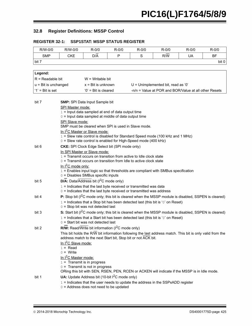
2014-2018 Microchip Technology Inc. DS40001775D-page 425
PIC16(L)F1764/5/8/9
32.8 Register Definitions: MSSP Control
REGISTER 32-1: SSP1STAT: MSSP STATUS REGISTER
R/W-0/0 R/W-0/0 R-0/0 R-0/0 R-0/0 R-0/0 R-0/0 R-0/0
SMP CKE D/A P S R/W UA BF
bit 7 bit 0
Legend:
R = Readable bit W = Writable bit
u = Bit is unchanged x = Bit is unknown U = Unimplemented bit, read as ‘0’
‘1’ = Bit is set ‘0’ = Bit is cleared -n/n = Value at POR and BOR/Value at all other Resets
bit 7 SMP: SPI Data Input Sample bit
SPI Master mode:1 = Input data sampled at end of data output time0 = Input data sampled at middle of data output time
SPI Slave mode:SMP must be cleared when SPI is used in Slave mode.
In I2 C Master or Slave mode: 1 = Slew rate control is disabled for Standard Speed mode (100 kHz and 1 MHz)0 = Slew rate control is enabled for High-Speed mode (400 kHz)
bit 6 CKE: SPI Clock Edge Select bit (SPI mode only)
In SPI Master or Slave mode:1 = Transmit occurs on transition from active to Idle clock state0 = Transmit occurs on transition from Idle to active clock state
In I2 C mode only: 1 = Enables input logic so that thresholds are compliant with SMBus specification0 = Disables SMBus specific inputs
bit 5 D/A: Data/Address bit (I2C mode only)
1 = Indicates that the last byte received or transmitted was data0 = Indicates that the last byte received or transmitted was address
bit 4 P: Stop bit (I2C mode only; this bit is cleared when the MSSP module is disabled, SSPEN is cleared)
1 = Indicates that a Stop bit has been detected last (this bit is ‘0’ on Reset)0 = Stop bit was not detected last
bit 3 S: Start bit (I2C mode only; this bit is cleared when the MSSP module is disabled, SSPEN is cleared)
1 = Indicates that a Start bit has been detected last (this bit is ‘0’ on Reset)0 = Start bit was not detected last
bit 2 R/W: Read/Write bit information (I2C mode only)
This bit holds the R/W bit information following the last address match. This bit is only valid from theaddress match to the next Start bit, Stop bit or not ACK bit.
In I2 C Slave mode:1 = Read0 = Write
In I2 C Master mode:1 = Transmit is in progress0 = Transmit is not in progressORing this bit with SEN, RSEN, PEN, RCEN or ACKEN will indicate if the MSSP is in Idle mode.
bit 1 UA: Update Address bit (10-bit I2C mode only)
1 = Indicates that the user needs to update the address in the SSPxADD register0 = Address does not need to be updated

2014-2018 Microchip Technology Inc. DS40001775D-page 426
PIC16(L)F1764/5/8/9
bit 0 BF: Buffer Full Status bit
Receive (SPI and I2 C modes):1 = Receive is complete, SSPxBUF is full0 = Receive is not complete, SSPxBUF is empty
Transmit (I2 C mode only):1 = Data transmit is in progress (does not include the ACK and Stop bits), SSPxBUF is full0 = Data transmit is complete (does not include the ACK and Stop bits), SSPxBUF is empty
REGISTER 32-1: SSP1STAT: MSSP STATUS REGISTER (CONTINUED)

2014-2018 Microchip Technology Inc. DS40001775D-page 427
PIC16(L)F1764/5/8/9
REGISTER 32-2: SSP1CON1: MSSP CONTROL REGISTER 1
R/C/HS-0/0 R/C/HS-0/0 R/W-0/0 R/W-0/0 R/W-0/0 R/W-0/0 R/W-0/0 R/W-0/0
WCOL SSPOV(1) SSPEN CKP SSPM<3:0>
bit 7 bit 0
Legend:
R = Readable bit W = Writable bit HS = Hardware Settable bit C = Clearable bit
u = Bit is unchanged x = Bit is unknown U = Unimplemented bit, read as ‘0’
‘1’ = Bit is set ‘0’ = Bit is cleared -n/n = Value at POR and BOR/Value at all other Resets
bit 7 WCOL: Write Collision Detect bit
Master mode:1 = A write to the SSPxBUF register was attempted while the I2C conditions were not valid for a
transmission to be started0 = No collision
Slave mode:1 = The SSPxBUF register is written while it is still transmitting the previous word (must be cleared in
software)0 = No collision
bit 6 SSPOV: Receive Overflow Indicator bit(1)
In SPI mode:1 = A new byte is received while the SSPxBUF register is still holding the previous data. In case of over-
flow, the data in SSPSR is lost. Overflow can only occur in Slave mode. In Slave mode, the user must read the SSPxBUF, even if only transmitting data, to avoid setting overflow. In Master mode, the over-flow bit is not set since each new reception (and transmission) is initiated by writing to the SSPxBUF register (must be cleared in software).
0 = No overflow
In I2 C mode:1 = A byte is received while the SSPxBUF register is still holding the previous byte. SSPOV is a “don’t
care” in Transmit mode (must be cleared in software). 0 = No overflow
bit 5 SSPEN: Synchronous Serial Port Enable bit
In both modes, when enabled, these pins must be properly configured as input or output.
In SPI mode:1 = Enables serial port and configures SCK, SDO, SDI and SS as the source of the serial port pins(2)
0 = Disables serial port and configures these pins as I/O port pins
In I2 C mode:1 = Enables the serial port and configures the SDA and SCL pins as the source of the serial port pins(3)
0 = Disables serial port and configures these pins as I/O port pins
Note 1: In Master mode, the overflow bit is not set since each new reception (and transmission) is initiated by writing to the SSPxBUF register.
2: When enabled, these pins must be properly configured as input or output. Use SSPSSPPS, SSPCLKPPS, SSPDATPPS and RxyPPS to select the pins.
3: When enabled, the SDA and SCL pins must be configured as inputs. Use SSPCLKPPS, SSPDATPPS and RxyPPS to select the pins.
4: SSPxADD values of 0, 1 or 2 are not supported for I2C mode.
5: SSPxADD value of 0 is not supported; use SSPM<3:0> = 0000 instead.
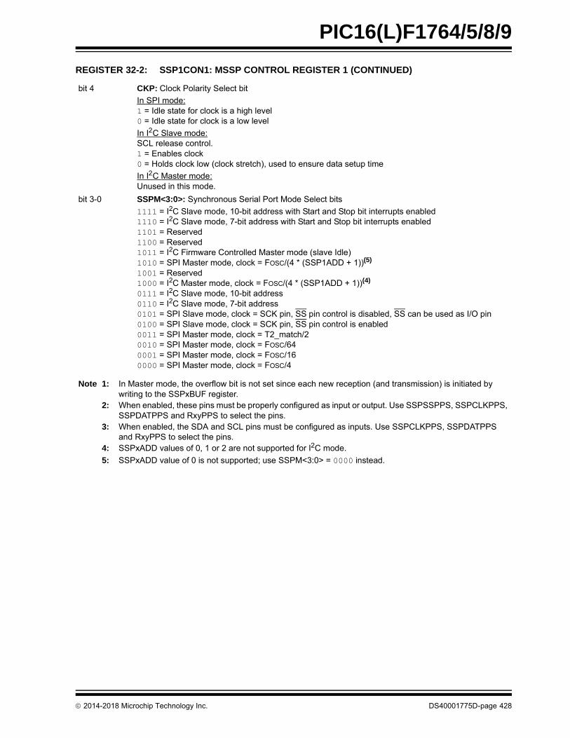
2014-2018 Microchip Technology Inc. DS40001775D-page 428
PIC16(L)F1764/5/8/9
bit 4 CKP: Clock Polarity Select bit
In SPI mode:1 = Idle state for clock is a high level 0 = Idle state for clock is a low level
In I2 C Slave mode:SCL release control.1 = Enables clock 0 = Holds clock low (clock stretch), used to ensure data setup time
In I2 C Master mode:Unused in this mode.
bit 3-0 SSPM<3:0>: Synchronous Serial Port Mode Select bits
1111 = I2C Slave mode, 10-bit address with Start and Stop bit interrupts enabled 1110 = I2C Slave mode, 7-bit address with Start and Stop bit interrupts enabled 1101 = Reserved 1100 = Reserved 1011 = I2C Firmware Controlled Master mode (slave Idle) 1010 = SPI Master mode, clock = FOSC/(4 * (SSP1ADD + 1))(5)
1001 = Reserved1000 = I2C Master mode, clock = FOSC/(4 * (SSP1ADD + 1))(4)
0111 = I2C Slave mode, 10-bit address 0110 = I2C Slave mode, 7-bit address 0101 = SPI Slave mode, clock = SCK pin, SS pin control is disabled, SS can be used as I/O pin0100 = SPI Slave mode, clock = SCK pin, SS pin control is enabled 0011 = SPI Master mode, clock = T2_match/2 0010 = SPI Master mode, clock = FOSC/64 0001 = SPI Master mode, clock = FOSC/16 0000 = SPI Master mode, clock = FOSC/4
REGISTER 32-2: SSP1CON1: MSSP CONTROL REGISTER 1 (CONTINUED)
Note 1: In Master mode, the overflow bit is not set since each new reception (and transmission) is initiated by writing to the SSPxBUF register.
2: When enabled, these pins must be properly configured as input or output. Use SSPSSPPS, SSPCLKPPS, SSPDATPPS and RxyPPS to select the pins.
3: When enabled, the SDA and SCL pins must be configured as inputs. Use SSPCLKPPS, SSPDATPPS and RxyPPS to select the pins.
4: SSPxADD values of 0, 1 or 2 are not supported for I2C mode.
5: SSPxADD value of 0 is not supported; use SSPM<3:0> = 0000 instead.

2014-2018 Microchip Technology Inc. DS40001775D-page 429
PIC16(L)F1764/5/8/9
REGISTER 32-3: SSP1CON2: MSSP CONTROL REGISTER 2(1)
R/W-0/0 R-0/0 R/W-0/0 R/S/HS-0/0 R/S/HS-0/0 R/S/HS-0/0 R/S/HS-0/0 R/W/HS-0/0
GCEN ACKSTAT ACKDT ACKEN RCEN PEN RSEN SEN
bit 7 bit 0
Legend:
R = Readable bit W = Writable bit HS = Hardware Settable bit S = Settable bit
u = Bit is unchanged x = Bit is unknown U = Unimplemented bit, read as ‘0’
‘1’ = Bit is set ‘0’ = Bit is cleared -n/n = Value at POR and BOR/Value at all other Resets
bit 7 GCEN: General Call Enable bit (in I2C Slave mode only)
1 = Enables interrupt when a general call address (0x00 or 00h) is received in the SSPSR0 = General call address disabled
bit 6 ACKSTAT: Acknowledge Status bit (in I2C mode only)
1 = Acknowledge was not received0 = Acknowledge was received
bit 5 ACKDT: Acknowledge Data bit (in I2C mode only)
In Receive mode:Value transmitted when the user initiates an Acknowledge sequence at the end of a receive.1 = Not Acknowledge0 = Acknowledge
bit 4 ACKEN: Acknowledge Sequence Enable bit (in I2C Master mode only)
In Master Receive mode:1 = Initiate Acknowledge sequence on SDA and SCL pins, and transmit ACKDT data bit;
automatically cleared by hardware0 = Acknowledge sequence is Idle
bit 3 RCEN: Receive Enable bit (in I2C Master mode only)
1 = Enables Receive mode for I2C0 = Receive is Idle
bit 2 PEN: Stop Condition Enable bit (in I2C Master mode only)
SCKMSSP Release Control:1 = Initiates Stop condition on SDA and SCL pins; automatically cleared by hardware0 = Stop condition is Idle
bit 1 RSEN: Repeated Start Condition Enable bit (in I2C Master mode only)
1 = Initiates Repeated Start condition on SDA and SCL pins; automatically cleared by hardware0 = Repeated Start condition is Idle
bit 0 SEN: Start Condition Enable/Stretch Enable bit
In Master mode:1 = Initiates Start condition on SDA and SCL pins; automatically cleared by hardware0 = Start condition is Idle
In Slave mode:1 = Clock stretching is enabled for both slave transmit and slave receive (stretch enabled)0 = Clock stretching is disabled
Note 1: For bits ACKEN, RCEN, PEN, RSEN, SEN: If the I2C module is not in Idle mode, this bit may not be set (no spooling) and the SSPxBUF may not be written (or writes to the SSPxBUF are disabled).

2014-2018 Microchip Technology Inc. DS40001775D-page 430
PIC16(L)F1764/5/8/9
REGISTER 32-4: SSP1CON3: MSSP CONTROL REGISTER 3
R-0/0 R/W-0/0 R/W-0/0 R/W-0/0 R/W-0/0 R/W-0/0 R/W-0/0 R/W-0/0
ACKTIM(3) PCIE SCIE BOEN SDAHT SBCDE AHEN DHEN
bit 7 bit 0
Legend:
R = Readable bit W = Writable bit
u = Bit is unchanged x = Bit is unknown U = Unimplemented bit, read as ‘0’
‘1’ = Bit is set ‘0’ = Bit is cleared -n/n = Value at POR and BOR/Value at all other Resets
bit 7 ACKTIM: Acknowledge Time Status bit (I2C slave modes only)(3)
1 = Indicates the I2C bus is in an Acknowledge sequence, set on eighth falling edge of SCL clock0 = Not an Acknowledge sequence, cleared on 9th rising edge of SCL clock
bit 6 PCIE: Stop Condition Interrupt Enable bit (I2C slave modes only)
1 = Enables interrupt on detection of Stop condition0 = Stop detection interrupts are disabled(2)
bit 5 SCIE: Start Condition Interrupt Enable bit (I2C slave modes only)
1 = Enables interrupt on detection of Start or Restart conditions0 = Start detection interrupts are disabled(2)
bit 4 BOEN: Buffer Overwrite Enable bit
In SPI Slave mode:(1)
1 = SSPxBUF updates every time that a new data byte is shifted in, ignoring the BF bit0 = If new byte is received with BF bit of the SSPxSTAT register already set, the SSPOV bit of the
SSPxCON1 register is set and the buffer is not updated
In I2 C Master mode and SPI Master mode:This bit is ignored.
In I2 C Slave mode:1 = SSPxBUF is updated and ACK is generated for a received address/data byte, ignoring the state
of the SSPOV bit only if the BF bit = 00 = SSPxBUF is only updated when SSPOV is clear
bit 3 SDAHT: SDA Hold Time Selection bit (I2C mode only)
1 = Minimum of 300 ns hold time on SDA after the falling edge of SCL0 = Minimum of 100 ns hold time on SDA after the falling edge of SCL
bit 2 SBCDE: Slave Mode Bus Collision Detect Enable bit (I2C Slave mode only)
If, on the rising edge of SCL, SDA is sampled low when the module is outputting a high state, theBCL1IF bit of the PIR2 register is set and the bus goes Idle1 = Enables slave bus collision interrupts0 = Slave bus collision interrupts are disabled
bit 1 AHEN: Address Hold Enable bit (I2C Slave mode only)
1 = Following the eighth falling edge of SCL for a matching received address byte; CKP bit of theSSPxCON1 register will be cleared and the SCL will be held low
0 = Address holding is disabled
bit 0 DHEN: Data Hold Enable bit (I2C Slave mode only)
1 = Following the eighth falling edge of SCL for a received data byte; slave hardware clears the CKPbit of the SSPxCON1 register and SCL is held low
0 = Data holding is disabled
Note 1: For daisy-chained SPI operation; allows the user to ignore all but the last received byte. SSPOV is still set when a new byte is received and BF = 1, but hardware continues to write the most recent byte to SSP1BUF.
2: This bit has no effect in Slave modes in which Start and Stop condition detection is explicitly listed as enabled.
3: The ACKTIM status bit is only active when the AHEN bit or DHEN bit is set.

2014-2018 Microchip Technology Inc. DS40001775D-page 431
PIC16(L)F1764/5/8/9
REGISTER 32-5: SSP1MSK: MSSP MASK REGISTER
R/W-1/1 R/W-1/1 R/W-1/1 R/W-1/1 R/W-1/1 R/W-1/1 R/W-1/1 R/W-1/1
MSK<7:0>
bit 7 bit 0
Legend:
R = Readable bit W = Writable bit
u = Bit is unchanged x = Bit is unknown U = Unimplemented bit, read as ‘0’
‘1’ = Bit is set ‘0’ = Bit is cleared -n/n = Value at POR and BOR/Value at all other Resets
bit 7-1 MSK<7:1>: Mask bits
1 = The received address bit n is compared to SSPxADD<n> to detect I2C address match0 = The received address bit n is not used to detect I2C address match
bit 0 MSK0: Mask for I2C Slave mode bit (10-Bit Address)
10-Bit Address, SSPM<3:0> = 0111 or 1111:1 = The received address bit 0 is compared to SSPxADD<0> to detect I2C address match0 = The received address bit 0 is not used to detect I2C address matchI2C Slave mode, 7-Bit Address, the bit is ignored.
REGISTER 32-6: SSP1ADD: MSSP ADDRESS AND BAUD RATE REGISTER (I2C MODE)
R/W-0/0 R/W-0/0 R/W-0/0 R/W-0/0 R/W-0/0 R/W-0/0 R/W-0/0 R/W-0/0
ADD<7:0>
bit 7 bit 0
Legend:
R = Readable bit W = Writable bit
u = Bit is unchanged x = Bit is unknown U = Unimplemented bit, read as ‘0’
‘1’ = Bit is set ‘0’ = Bit is cleared -n/n = Value at POR and BOR/Value at all other Resets
bit 7-0
Master mode:
ADD<7:0>: Baud Rate Clock Divider bits
SCL pin clock period = ((ADD<7:0> + 1) * 4)/FOSC.
bit 7-3
10-Bit Slave mode – Most Significant Address Byte:
ADD<7:3>: MSSP Address bits
Not Used: Unused for Most Significant Address Byte. Bit state of this register is a “don’t care”. Bitpattern sent by master is fixed by I2C specification and must be equal to ‘11110’. However, those bitsare compared by hardware and are not affected by the value in this register.
bit 2-1 ADD<2:1>: Two Most Significant 10-Bit Address bits
bit 0 ADD0: MSSP Address bit
Not Used: Unused in this mode. Bit state is a “don’t care”.
bit 7-0
10-Bit Slave mode – Least Significant Address Byte:
ADD<7:0>: Eight Least Significant 10-Bit Address bits
bit 7-1
7-Bit Slave mode:
ADD<7:1>: MSSP 7-Bit Address bits
bit 0 ADD0: MSSP Address bit
Not Used: Unused in this mode. Bit state is a “don’t care”.

2014-2018 Microchip Technology Inc. DS40001775D-page 432
PIC16(L)F1764/5/8/9
33.0 ENHANCED UNIVERSAL SYNCHRONOUS ASYNCHRONOUS RECEIVER TRANSMITTER (EUSART)
The Enhanced Universal Synchronous AsynchronousReceiver Transmitter (EUSART) module is a serial I/Ocommunications peripheral. It contains all the clockgenerators, shift registers and data buffers necessaryto perform an input or output serial data transferindependent of device program execution. TheEUSART, also known as a Serial CommunicationsInterface (SCI), can be configured as a full-duplexasynchronous system or half-duplex synchronous sys-tem. Full-Duplex mode is useful for communicationswith peripheral systems, such as CRT terminals andpersonal computers. Half-Duplex Synchronous modeis intended for communications with peripheraldevices, such as A/D or D/A integrated circuits, serialEEPROMs or other microcontrollers. These devicestypically do not have internal clocks for baud rate gen-eration and require the external clock signal providedby a master synchronous device.
The EUSART module includes the following capabilities:
• Full-duplex asynchronous transmit and receive• Two-character input buffer• One-character output buffer• Programmable 8-bit or 9-bit character length• Address detection in 9-bit mode• Input buffer overrun error detection• Received character framing error detection• Half-duplex synchronous master• Half-duplex synchronous slave• Programmable clock polarity in Synchronous modes• Sleep operation
The EUSART module implements the followingadditional features, making it ideally suited for use inLocal Interconnect Network (LIN) bus systems:
• Automatic detection and calibration of the baud rate• Wake-up on Break reception• 13-bit Break character transmit
Block diagrams of the EUSART transmitter andreceiver are shown in Figure 33-1 and Figure 33-2.
The EUSART transmit output (TX_out) is available tothe TX/CK pin and internally to the following peripherals:
• Configurable Logic Cell (CLC)• Data Signal Modulator (DSM)
FIGURE 33-1: EUSART TRANSMIT BLOCK DIAGRAM
TXIF
TXIE
Interrupt
TXEN
TX9D
MSb LSb
Data Bus
TXxREG Register
Transmit Shift Register (TSR)
(8) 0
TX9
TRMT
RX/DT
Pin Bufferand Control
8
SPxBRGLSPxBRGH
BRG16
FOSC÷ n
n
+ 1 Multiplier x4 x16 x64
SYNC 1 x 0 0 0
BRGH x 1 1 0 0
BRG16 x 1 0 1 0
Baud Rate Generator
• • •
TX_out
PPS
RxyPPS(1)
CK Pin
PPS
CKPPS
1
0
SYNCCSRC
TX/CK
PPS0
1
SYNCCSRC
RxyPPS
SYNC
Note 1: In Synchronous mode, the DT output and RX input PPS selections should enable the same pin.
Pin
Pin

2014-2018 Microchip Technology Inc. DS40001775D-page 433
PIC16(L)F1764/5/8/9
FIGURE 33-2: EUSART RECEIVE BLOCK DIAGRAM
The operation of the EUSART module is controlledthrough three registers:
• Transmit Status and Control (TXxSTA)
• Receive Status and Control (RCxSTA)
• Baud Rate Control (BAUDxCON)
These registers are detailed in Register 33-1,Register 33-2 and Register 33-3, respectively.
The RX and CK input pins are selected with the RXPPSand CKPPS registers, respectively. TX, CK and DToutput pins are selected with each pin’s RxyPPS register.Since the RX input is coupled with the DT output inSynchronous mode, it is the user’s responsibility to selectthe same pin for both of these functions when operatingin Synchronous mode. The EUSART control logic willcontrol the data direction drivers automatically.
RX/DT PinPin Buffer
and Control
SPEN
DataRecovery
CREN OERR
FERR
RSR RegisterMSb LSb
RX9D RCxREG RegisterFIFO
InterruptRCIFRCIE
Data Bus8
Stop Start(8) 7 1 0
RX9
• • •
SPxBRGLSPxBRGH
BRG16
RCIDL
FOSC÷ n
n+ 1 Multiplier x4 x16 x64
SYNC 1 x 0 0 0
BRGH x 1 1 0 0
BRG16 x 1 0 1 0
Baud Rate Generator
PPS
RXPPS(1)
Note 1: In Synchronous mode, the DT output and RX input PPS selections should enable the same pin.

2014-2018 Microchip Technology Inc. DS40001775D-page 434
PIC16(L)F1764/5/8/9
33.1 EUSART Asynchronous Mode
The EUSART transmits and receives data using thestandard Non-Return-to-Zero (NRZ) format. NRZ isimplemented with two levels: a VOH Mark state whichrepresents a ‘1’ data bit, and a VOL Space state whichrepresents a ‘0’ data bit. NRZ refers to the fact thatconsecutively transmitted data bits of the same valuestay at the output level of that bit without returning to aneutral level between each bit transmission. An NRZtransmission port Idles in the Mark state. Each charactertransmission consists of one Start bit, followed by eightor nine data bits and is always terminated by one ormore Stop bits. The Start bit is always a space and theStop bits are always marks. The most common dataformat is eight bits. Each transmitted bit persists for aperiod of 1/(Baud Rate). An on-chip dedicated8-bit/16-bit Baud Rate Generator is used to derivestandard baud rate frequencies from the systemoscillator. See Table 33-5 for examples of baud rateconfigurations.
The EUSART transmits and receives the LSb first. TheEUSART’s transmitter and receiver are functionallyindependent, but share the same data format and baudrate. Parity is not supported by the hardware, but canbe implemented in software and stored as the ninthdata bit.
33.1.1 EUSART ASYNCHRONOUS TRANSMITTER
The EUSART transmitter block diagram is shown inFigure 33-1. The heart of the transmitter is the serialTransmit Shift Register (TSR), which is not directlyaccessible by software. The TSR obtains its data fromthe transmit buffer, which is the TXxREG register.
33.1.1.1 Enabling the Transmitter
The EUSART transmitter is enabled for asynchronousoperations by configuring the following three controlbits:
• TXEN = 1
• SYNC = 0
• SPEN = 1
All other EUSART control bits are assumed to be intheir default state.
Setting the TXEN bit of the TXxSTA register enables thetransmitter circuitry of the EUSART. Clearing the SYNCbit of the TXxSTA register configures the EUSART forasynchronous operation. Setting the SPEN bit of theRCxSTA register enables the EUSART andautomatically configures the TX/CK I/O pin as an output.If the TX/CK pin is shared with an analog peripheral, theanalog I/O function must be disabled by clearing thecorresponding ANSELx bit.
33.1.1.2 Transmitting Data
A transmission is initiated by writing a character to theTXxREG register. If this is the first character, or theprevious character has been completely flushed fromthe TSR, the data in the TXxREG is immediatelytransferred to the TSR register. If the TSR still containsall or part of a previous character, the new characterdata is held in the TXxREG until the Stop bit of theprevious character has been transmitted. The pendingcharacter in the TXxREG is then transferred to the TSRin one TCY immediately following the Stop bittransmission. The transmission of the Start bit, data bitsand Stop bit sequence commences immediatelyfollowing the transfer of the data to the TSR from theTXxREG.
33.1.1.3 Transmit Data Polarity
The polarity of the transmit data can be controlled withthe SCKP bit of the BAUDxCON register. The defaultstate of this bit is ‘0’ which selects high true transmit Idleand data bits. Setting the SCKP bit to ‘1’ will invert thetransmit data resulting in low true Idle and data bits. TheSCKP bit controls transmit data polarity inAsynchronous mode only. In Synchronous mode, theSCKP bit has a different function. See Section 33.5.1.2“Clock Polarity”.
33.1.1.4 Transmit Interrupt Flag
The TXIF interrupt flag bit of the PIR1 register is setwhenever the EUSART transmitter is enabled and nocharacter is being held for transmission in the TXxREG.In other words, the TXIF bit is only clear when the TSRis busy with a character and a new character has beenqueued for transmission in the TXxREG. The TXIF flagbit is not cleared immediately upon writing TXxREG.TXIF becomes valid in the second instruction cyclefollowing the write execution. Polling TXIF immediatelyfollowing the TXxREG write will return invalid results.The TXIF bit is read-only, it cannot be set or cleared bysoftware.
The TXIF interrupt can be enabled by setting the TXIEinterrupt enable bit of the PIE1 register. However, theTXIF flag bit will be set whenever the TXxREG isempty, regardless of the state of TXIE enable bit.
To use interrupts when transmitting data, set the TXIEbit only when there is more data to send. Clear theTXIE interrupt enable bit upon writing the last characterof the transmission to the TXxREG.
Note: The TXIF transmitter interrupt flag is setwhen the TXEN enable bit is set.

2014-2018 Microchip Technology Inc. DS40001775D-page 435
PIC16(L)F1764/5/8/9
33.1.1.5 TSR Status
The TRMT bit of the TXxSTA register indicates thestatus of the TSR register. This is a read-only bit. TheTRMT bit is set when the TSR register is empty and iscleared when a character is transferred to the TSRregister from the TXxREG. The TRMT bit remains clearuntil all bits have been shifted out of the TSR register.No interrupt logic is tied to this bit, so the user has topoll this bit to determine the TSR status.
33.1.1.6 Transmitting 9-Bit Characters
The EUSART supports 9-bit character transmissions.When the TX9 bit of the TXxSTA register is set, theEUSART will shift nine bits out for each character trans-mitted. The TX9D bit of the TXxSTA register is theninth, and Most Significant data bit. When transmitting9-bit data, the TX9D data bit must be written beforewriting the eight Least Significant bits into the TXxREG.All nine bits of data will be transferred to the TSR shiftregister immediately after the TXxREG is written.
A special 9-Bit Address mode is available for use withmultiple receivers. See Section 33.1.2.7 “AddressDetection” for more information on the Address mode.
33.1.1.7 Asynchronous Transmission Setup
1. Initialize the SPxBRGH, SPxBRGL register pairand the BRGH and BRG16 bits to achieve thedesired baud rate (see Section 33.4 “EUSARTBaud Rate Generator (BRG)”).
2. Enable the asynchronous serial port by clearingthe SYNC bit and setting the SPEN bit.
3. If 9-bit transmission is desired, set the TX9control bit. A set ninth data bit will indicate thatthe eight Least Significant data bits are anaddress when the receiver is set for addressdetection.
4. Set SCKP bit if inverted transmit is desired.
5. Enable the transmission by setting the TXENcontrol bit. This will cause the TXIF interrupt bitto be set.
6. If interrupts are desired, set the TXIE interruptenable bit of the PIE1 register. An interrupt willoccur immediately provided that the GIE andPEIE bits of the INTCON register are also set.
7. If 9-bit transmission is selected, the ninth bitshould be loaded into the TX9D data bit.
8. Load 8-bit data into the TXxREG register. Thiswill start the transmission.
FIGURE 33-3: ASYNCHRONOUS TRANSMISSION
Note: The TSR register is not mapped in datamemory, so it is not available to the user.
Word 1
Word 1Transmit Shift Reg.
Start bit bit 0 bit 1 bit 7/8
Write to TXxREG
BRG Output(Shift Clock)
TX/CK Pin
TXIF bit(Transmit Buffer
Reg. Empty Flag)
TRMT bit(Transmit Shift
Reg. Empty Flag)
1 TCY
Word 1
Stop bit
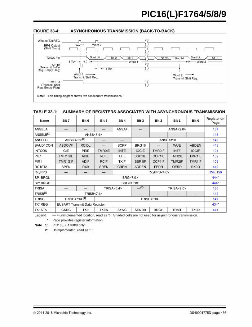
2014-2018 Microchip Technology Inc. DS40001775D-page 436
PIC16(L)F1764/5/8/9
FIGURE 33-4: ASYNCHRONOUS TRANSMISSION (BACK-TO-BACK)
TABLE 33-1: SUMMARY OF REGISTERS ASSOCIATED WITH ASYNCHRONOUS TRANSMISSION
Name Bit 7 Bit 6 Bit 5 Bit 4 Bit 3 Bit 2 Bit 1 Bit 0Register on
Page
ANSELA — — — ANSA4 — ANSA<2:0> 137
ANSELB(1) ANSB<7:4> — — — — 143
ANSELC ANSC<7:6>(1) — — ANSC<3:0> 148
BAUD1CON ABDOVF RCIDL — SCKP BRG16 — WUE ABDEN 443
INTCON GIE PEIE TMR0IE INTE IOCIE TMR0IF INTF IOCIF 101
PIE1 TMR1GIE ADIE RCIE TXIE SSP1IE CCP1IE TMR2IE TMR1IE 102
PIR1 TMR1GIF ADIF RCIF TXIF SSP1IF CCP1IF TMR2IF TMR1IF 105
RC1STA SPEN RX9 SREN CREN ADDEN FERR OERR RX9D 442
RxyPPS — — — RxyPPS<4:0> 154, 156
SP1BRGL BRG<7:0> 444*
SP1BRGH BRG<15:8> 444*
TRISA — — TRISA<5:4> —(2) TRISA<2:0> 136
TRISB(1) TRISB<7:4> — — — — 142
TRISC TRISC<7:6>(1) TRISC<5:0> 147
TX1REG EUSART Transmit Data Register 434*
TX1STA CSRC TX9 TXEN SYNC SENDB BRGH TRMT TX9D 441
Legend: — = unimplemented location, read as ‘0’. Shaded cells are not used for asynchronous transmission.
* Page provides register information.
Note 1: PIC16(L)F1768/9 only.
2: Unimplemented, read as ‘1’.
Transmit Shift Reg.
Write to TXxREG
BRG Output(Shift Clock)
TX/CK Pin
TRMT bit(Transmit Shift
Reg. Empty Flag)
Word 1 Word 2
Word 1 Word 2
Start bit Stop bit Start bit
Transmit Shift Reg.
Word 1 Word 2bit 0 bit 1 bit 7/8 bit 0
Note: This timing diagram shows two consecutive transmissions.
1 TCY
1 TCY
TXIF bit(Transmit Buffer
Reg. Empty Flag)

2014-2018 Microchip Technology Inc. DS40001775D-page 437
PIC16(L)F1764/5/8/9
33.1.2 EUSART ASYNCHRONOUS RECEIVER
The Asynchronous mode is typically used in RS-232systems. The receiver block diagram is shown inFigure 33-2. The data is received on the RX/DT pin anddrives the data recovery block. The data recovery blockis actually a high-speed shifter operating at 16 timesthe baud rate, whereas the serial Receive ShiftRegister (RSR) operates at the bit rate. When all eightor nine bits of the character have been shifted in, theyare immediately transferred to a two-characterFirst-In-First-Out (FIFO) memory. The FIFO bufferingallows reception of two complete characters and thestart of a third character before software must startservicing the EUSART receiver. The FIFO and RSRregisters are not directly accessible by software.Access to the received data is via the RCxREGregister.
33.1.2.1 Enabling the Receiver
The EUSART receiver is enabled for asynchronousoperation by configuring the following three control bits:
• CREN = 1
• SYNC = 0
• SPEN = 1
All other EUSART control bits are assumed to be intheir default state.
Setting the CREN bit of the RCxSTA register enablesthe receiver circuitry of the EUSART. Clearing the SYNCbit of the TXxSTA register configures the EUSART forasynchronous operation. Setting the SPEN bit of theRCxSTA register enables the EUSART. The programmermust set the corresponding TRIS bit to configure theRX/DT I/O pin as an input.
33.1.2.2 Receiving Data
The receiver data recovery circuit initiates characterreception on the falling edge of the first bit. The first bit,also known as the Start bit, is always a zero. The datarecovery circuit counts one-half bit time to the center ofthe Start bit and verifies that the bit is still a zero. If it isnot a zero then the data recovery circuit aborts charac-ter reception, without generating an error, and resumeslooking for the falling edge of the Start bit. If the Start bitzero verification succeeds, then the data recoverycircuit counts a full bit time to the center of the next bit.The bit is then sampled by a majority detect circuit andthe resulting ‘0’ or ‘1’ is shifted into the RSR. Thisrepeats until all data bits have been sampled andshifted into the RSR. One final bit time is measured andthe level sampled. This is the Stop bit, which is alwaysa ‘1’. If the data recovery circuit samples a ‘0’ in theStop bit position then a framing error is set for this char-acter, otherwise the framing error is cleared for thischaracter. See Section 33.1.2.4 “Receive FramingError” for more information on framing errors.
Immediately after all data bits and the Stop bit havebeen received, the character in the RSR is transferredto the EUSART receive FIFO and the RCIF interruptflag bit of the PIR1 register is set. The top character inthe FIFO is transferred out of the FIFO by reading theRCxREG register.
33.1.2.3 Receive Interrupts
The RCIF interrupt flag bit of the PIR1 register is setwhenever the EUSART receiver is enabled and there isan unread character in the receive FIFO. The RCIFinterrupt flag bit is read-only; it cannot be set or clearedby software.
RCIF interrupts are enabled by setting all of thefollowing bits:
• RCIE, Interrupt Enable bit of the PIE1 register
• PEIE, Peripheral Interrupt Enable bit of the INTCON register
• GIE, Global Interrupt Enable bit of the INTCON register
The RCIF interrupt flag bit will be set when there is anunread character in the FIFO, regardless of the state ofinterrupt enable bits.
Note: If the RX/DT function is on an analog pin,the corresponding ANSELx bit must becleared for the receiver to function.
Note: If the receive FIFO is overrun, no additionalcharacters will be received until the overruncondition is cleared. See Section 33.1.2.5“Receive Overrun Error” for moreinformation on overrun errors.

2014-2018 Microchip Technology Inc. DS40001775D-page 438
PIC16(L)F1764/5/8/9
33.1.2.4 Receive Framing Error
Each character in the receive FIFO buffer has acorresponding framing error status bit. A framing errorindicates that a Stop bit was not seen at the expectedtime. The framing error status is accessed via theFERR bit of the RCxSTA register. The FERR bitrepresents the status of the top unread character in thereceive FIFO. Therefore, the FERR bit must be readbefore reading the RCxREG.
The FERR bit is read-only and only applies to the topunread character in the receive FIFO. A framing error(FERR = 1) does not preclude reception of additionalcharacters. It is not necessary to clear the FERR bit.Reading the next character from the FIFO buffer willadvance the FIFO to the next character and the nextcorresponding framing error.
The FERR bit can be forced clear by clearing the SPENbit of the RCxSTA register which resets the EUSART.Clearing the CREN bit of the RCxSTA register does notaffect the FERR bit. A framing error by itself does notgenerate an interrupt.
33.1.2.5 Receive Overrun Error
The receive FIFO buffer can hold two characters. Anoverrun error will be generated if a third character, in itsentirety, is received before the FIFO is accessed. Whenthis happens, the OERR bit of the RCxSTA register isset. The characters already in the FIFO buffer can beread, but no additional characters will be received untilthe error is cleared. The error must be cleared by eitherclearing the CREN bit of the RCxSTA register or byresetting the EUSART by clearing the SPEN bit of theRCxSTA register.
33.1.2.6 Receiving 9-Bit Characters
The EUSART supports 9-bit character reception. Whenthe RX9 bit of the RCxSTA register is set, the EUSARTwill shift nine bits into the RSR for each characterreceived. The RX9D bit of the RCxSTA register is theninth and Most Significant data bit of the top unreadcharacter in the receive FIFO. When reading 9-bit datafrom the receive FIFO buffer, the RX9D data bit mustbe read before reading the eight Least Significant bitsfrom the RCxREG.
33.1.2.7 Address Detection
A special Address Detection mode is available for usewhen multiple receivers share the same transmissionline, such as in RS-485 systems. Address detection isenabled by setting the ADDEN bit of the RCxSTAregister.
Address detection requires 9-bit character reception.When address detection is enabled, only characterswith the ninth data bit set will be transferred to thereceive FIFO buffer, thereby setting the RCIF interruptbit. All other characters will be ignored.
Upon receiving an address character, user softwaredetermines if the address matches its own. Uponaddress match, user software must disable addressdetection by clearing the ADDEN bit before the nextStop bit occurs. When user software detects the end ofthe message, determined by the message protocolused, software places the receiver back into theAddress Detection mode by setting the ADDEN bit.
Note: If all receive characters in the receiveFIFO have framing errors, repeated readsof the RCxREG will not clear the FERR bit.
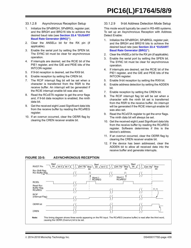
2014-2018 Microchip Technology Inc. DS40001775D-page 439
PIC16(L)F1764/5/8/9
33.1.2.8 Asynchronous Reception Setup
1. Initialize the SPxBRGH, SPxBRGL register pair,and the BRGH and BRG16 bits to achieve thedesired baud rate (see Section 33.4 “EUSARTBaud Rate Generator (BRG)”).
2. Clear the ANSELx bit for the RX pin (ifapplicable).
3. Enable the serial port by setting the SPEN bit.The SYNC bit must be clear for asynchronousoperation.
4. If interrupts are desired, set the RCIE bit of thePIE1 register, and the GIE and PEIE bits of theINTCON register.
5. If 9-bit reception is desired, set the RX9 bit.
6. Enable reception by setting the CREN bit.
7. The RCIF interrupt flag bit will be set when acharacter is transferred from the RSR to thereceive buffer. An interrupt will be generated ifthe RCIE interrupt enable bit was also set.
8. Read the RCxSTA register to get the error flagsand, if 9-bit data reception is enabled, the ninthdata bit.
9. Get the received eight Least Significant data bitsfrom the receive buffer by reading the RCxREGregister.
10. If an overrun occurred, clear the OERR flag byclearing the CREN receiver enable bit.
33.1.2.9 9-bit Address Detection Mode Setup
This mode would typically be used in RS-485 systems.To set up an Asynchronous Reception with AddressDetect Enable:
1. Initialize the SPxBRGH, SPxBRGL register pair,and the BRGH and BRG16 bits to achieve thedesired baud rate (see Section 33.4 “EUSARTBaud Rate Generator (BRG)”).
2. Clear the ANSELx bit for the RX pin (if applicable).
3. Enable the serial port by setting the SPEN bit.The SYNC bit must be clear for asynchronousoperation.
4. If interrupts are desired, set the RCIE bit of thePIE1 register, and the GIE and PEIE bits of theINTCON register.
5. Enable 9-bit reception by setting the RX9 bit.
6. Enable address detection by setting the ADDENbit.
7. Enable reception by setting the CREN bit.
8. The RCIF interrupt flag bit will be set when acharacter with the ninth bit set is transferredfrom the RSR to the receive buffer. An interruptwill be generated if the RCIE interrupt enable bitwas also set.
9. Read the RCxSTA register to get the error flags.The ninth data bit will always be set.
10. Get the received eight Least Significant data bitsfrom the receive buffer by reading the RCxREGregister. Software determines if this is thedevice’s address.
11. If an overrun occurred, clear the OERR flag byclearing the CREN receiver enable bit.
12. If the device has been addressed, clear theADDEN bit to allow all received data into thereceive buffer and generate interrupts.
FIGURE 33-5: ASYNCHRONOUS RECEPTION
Startbit bit 7/8bit 1bit 0 bit 7/8 bit 0Stop
bit
Startbit
Startbitbit 7/8 Stop
bitRX/DT Pin
Rcv Buffer Reg.Rcv Shift Reg.
Read RcvBuffer Reg.RCxREG
RCIF(Interrupt Flag)
OERR bit
CREN
Word 1RCxREG
Word 2RCxREG
Stopbit
Note: This timing diagram shows three words appearing on the RX input. The RCxREG (receive buffer) is read after the third word,causing the OERR (Overrun) bit to be set.
RCIDL

2014-2018 Microchip Technology Inc. DS40001775D-page 440
PIC16(L)F1764/5/8/9
TABLE 33-2: SUMMARY OF REGISTERS ASSOCIATED WITH ASYNCHRONOUS RECEPTION
33.2 Clock Accuracy with Asynchronous Operation
The factory calibrates the Internal Oscillator Block(INTOSC) output. However, the INTOSC frequencymay drift as VDD or temperature changes and thisdirectly affects the asynchronous baud rate. Twomethods may be used to adjust the baud rate clock, butboth require a reference clock source of some kind.
The first (preferred) method uses the OSCTUNEregister to adjust the INTOSC output. Adjusting thevalue in the OSCTUNE register allows for fine resolutionchanges to the system clock source. SeeSection 5.2.2.3 “Internal Oscillator FrequencyAdjustment” for more information.
The other method adjusts the value in the Baud RateGenerator. This can be done automatically with theAuto-Baud Detect feature (see Section 33.4.1“Auto-Baud Detect”). There may not be fine enoughresolution when adjusting the Baud Rate Generator tocompensate for a gradual change in the peripheralclock frequency.
Name Bit 7 Bit 6 Bit 5 Bit 4 Bit 3 Bit 2 Bit 1 Bit 0Register on Page
ANSELA — — — ANSA4 — ANSA<2:0> 137
ANSELB(1) ANSB<7:4> — — — — 143
ANSELC ANSC<7:6>(1) — — ANSC<3:0> 148
BAUD1CON ABDOVF RCIDL — SCKP BRG16 — WUE ABDEN 443
INTCON GIE PEIE TMR0IE INTE IOCIE TMR0IF INTF IOCIF 101
PIE1 TMR1GIE ADIE RCIE TXIE SSP1IE CCP1IE TMR2IE TMR1IE 102
PIR1 TMR1GIF ADIF RCIF TXIF SSP1IF CCP1IF TMR2IF TMR1IF 105
RC1REG EUSART Receive Data Register 437*
RC1STA SPEN RX9 SREN CREN ADDEN FERR OERR RX9D 442
RxyPPS — — — RxyPPS<4:0> 154
SP1BRGL BRG<7:0> 444
SP1BRGH BRG<15:8> 444
TRISA — — TRISA<5:4> —(2) TRISA<2:0> 136
TRISB(1) TRISB<7:4> — — — — 142
TRISC TRISC<7:6>(1) TRISC<5:0> 147
TX1STA CSRC TX9 TXEN SYNC SENDB BRGH TRMT TX9D 441
Legend: — = unimplemented location, read as ‘0’. Shaded cells are not used for asynchronous reception.
* Page provides register information.
Note 1: PIC16(L)F1768/9 only.
2: Unimplemented, read as ‘1’.
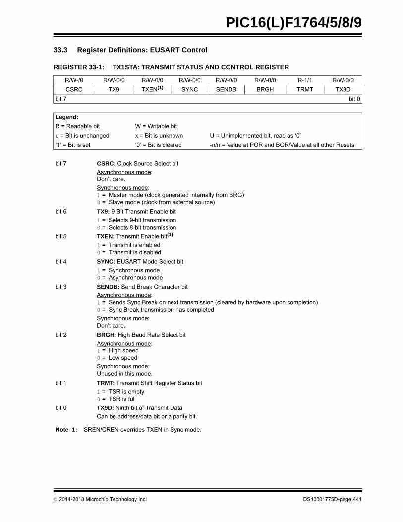
2014-2018 Microchip Technology Inc. DS40001775D-page 441
PIC16(L)F1764/5/8/9
33.3 Register Definitions: EUSART Control
REGISTER 33-1: TX1STA: TRANSMIT STATUS AND CONTROL REGISTER
R/W-/0 R/W-0/0 R/W-0/0 R/W-0/0 R/W-0/0 R/W-0/0 R-1/1 R/W-0/0
CSRC TX9 TXEN(1) SYNC SENDB BRGH TRMT TX9D
bit 7 bit 0
Legend:
R = Readable bit W = Writable bit
u = Bit is unchanged x = Bit is unknown U = Unimplemented bit, read as ‘0’
‘1’ = Bit is set ‘0’ = Bit is cleared -n/n = Value at POR and BOR/Value at all other Resets
bit 7 CSRC: Clock Source Select bit
Asynchronous mode: Don’t care.
Synchronous mode: 1 = Master mode (clock generated internally from BRG)0 = Slave mode (clock from external source)
bit 6 TX9: 9-Bit Transmit Enable bit
1 = Selects 9-bit transmission0 = Selects 8-bit transmission
bit 5 TXEN: Transmit Enable bit(1)
1 = Transmit is enabled0 = Transmit is disabled
bit 4 SYNC: EUSART Mode Select bit
1 = Synchronous mode 0 = Asynchronous mode
bit 3 SENDB: Send Break Character bit
Asynchronous mode:1 = Sends Sync Break on next transmission (cleared by hardware upon completion)0 = Sync Break transmission has completed
Synchronous mode:Don’t care.
bit 2 BRGH: High Baud Rate Select bit
Asynchronous mode: 1 = High speed 0 = Low speed
Synchronous mode: Unused in this mode.
bit 1 TRMT: Transmit Shift Register Status bit
1 = TSR is empty 0 = TSR is full
bit 0 TX9D: Ninth bit of Transmit Data
Can be address/data bit or a parity bit.
Note 1: SREN/CREN overrides TXEN in Sync mode.

2014-2018 Microchip Technology Inc. DS40001775D-page 442
PIC16(L)F1764/5/8/9
REGISTER 33-2: RC1STA: RECEIVE STATUS AND CONTROL REGISTER
R/W-0/0 R/W-0/0 R/W-0/0 R/W-0/0 R/W-0/0 R-0/0 R-0/0 R-0/0
SPEN RX9 SREN CREN ADDEN FERR OERR RX9D
bit 7 bit 0
Legend:
R = Readable bit W = Writable bit
u = Bit is unchanged x = Bit is unknown U = Unimplemented bit, read as ‘0’
‘1’ = Bit is set ‘0’ = Bit is cleared -n/n = Value at POR and BOR/Value at all other Resets
bit 7 SPEN: Serial Port Enable bit
1 = Serial port is enabled0 = Serial port is disabled (held in Reset)
bit 6 RX9: 9-Bit Receive Enable bit
1 = Selects 9-bit reception0 = Selects 8-bit reception
bit 5 SREN: Single Receive Enable bit
Asynchronous mode: Don’t care.
Synchronous mode – Master:1 = Enables single receive0 = Disables single receiveThis bit is cleared after reception is complete.
Synchronous mode – Slave:Don’t care.
bit 4 CREN: Continuous Receive Enable bit
Asynchronous mode:1 = Enables receiver0 = Disables receiver
Synchronous mode: 1 = Enables continuous receive until enable bit, CREN, is cleared (CREN overrides SREN)0 = Disables continuous receive
bit 3 ADDEN: Address Detect Enable bit
Asynchronous mode, 9-bit (RX9 = 1):1 = Enables address detection, enables interrupt and loads the receive buffer when RSR<8> is set0 = Disables address detection, all bytes are received and ninth bit can be used as parity bit
Asynchronous mode, 8-bit (RX9 = 0):Don’t care.
bit 2 FERR: Framing Error bit
1 = Framing error (can be updated by reading RCxREG register and receiving next valid byte)0 = No framing error
bit 1 OERR: Overrun Error bit
1 = Overrun error (can be cleared by clearing bit, CREN) 0 = No overrun error
bit 0 RX9D: Ninth bit of Received Data
This can be address/data bit or a parity bit and must be calculated by user firmware.
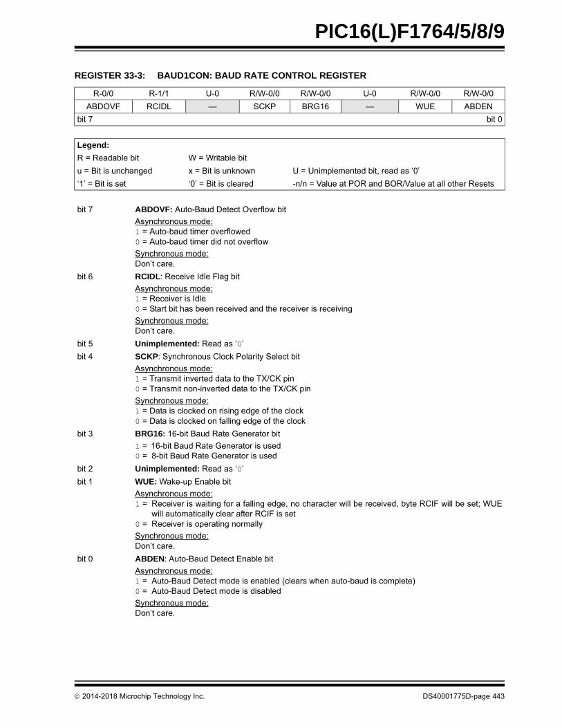
2014-2018 Microchip Technology Inc. DS40001775D-page 443
PIC16(L)F1764/5/8/9
REGISTER 33-3: BAUD1CON: BAUD RATE CONTROL REGISTER
R-0/0 R-1/1 U-0 R/W-0/0 R/W-0/0 U-0 R/W-0/0 R/W-0/0
ABDOVF RCIDL — SCKP BRG16 — WUE ABDEN
bit 7 bit 0
Legend:
R = Readable bit W = Writable bit
u = Bit is unchanged x = Bit is unknown U = Unimplemented bit, read as ‘0’
‘1’ = Bit is set ‘0’ = Bit is cleared -n/n = Value at POR and BOR/Value at all other Resets
bit 7 ABDOVF: Auto-Baud Detect Overflow bit
Asynchronous mode:1 = Auto-baud timer overflowed0 = Auto-baud timer did not overflow
Synchronous mode:Don’t care.
bit 6 RCIDL: Receive Idle Flag bit
Asynchronous mode:1 = Receiver is Idle0 = Start bit has been received and the receiver is receiving
Synchronous mode:Don’t care.
bit 5 Unimplemented: Read as ‘0’
bit 4 SCKP: Synchronous Clock Polarity Select bit
Asynchronous mode:1 = Transmit inverted data to the TX/CK pin0 = Transmit non-inverted data to the TX/CK pin
Synchronous mode:1 = Data is clocked on rising edge of the clock0 = Data is clocked on falling edge of the clock
bit 3 BRG16: 16-bit Baud Rate Generator bit
1 = 16-bit Baud Rate Generator is used0 = 8-bit Baud Rate Generator is used
bit 2 Unimplemented: Read as ‘0’
bit 1 WUE: Wake-up Enable bit
Asynchronous mode:1 = Receiver is waiting for a falling edge, no character will be received, byte RCIF will be set; WUE
will automatically clear after RCIF is set0 = Receiver is operating normally
Synchronous mode:Don’t care.
bit 0 ABDEN: Auto-Baud Detect Enable bit
Asynchronous mode:1 = Auto-Baud Detect mode is enabled (clears when auto-baud is complete)0 = Auto-Baud Detect mode is disabled
Synchronous mode:Don’t care.

2014-2018 Microchip Technology Inc. DS40001775D-page 444
PIC16(L)F1764/5/8/9
33.4 EUSART Baud Rate Generator (BRG)
The Baud Rate Generator (BRG) is an 8-bit or 16-bittimer that is dedicated to the support of both theasynchronous and synchronous EUSART operation.By default, the BRG operates in 8-bit mode. Setting theBRG16 bit of the BAUDxCON register selects 16-bitmode.
The SPxBRGH, SPxBRGL register pair determines theperiod of the free-running baud rate timer. InAsynchronous mode, the multiplier of the baud rateperiod is determined by both the BRGH bit of theTXxSTA register and the BRG16 bit of the BAUDxCONregister. In Synchronous mode, the BRGH bit is ignored.
Table 33-3 contains the formulas for determining thebaud rate. Example 33-1 provides a sample calculationfor determining the baud rate and baud rate error.
Typical baud rates and error values for variousAsynchronous modes have been computed for yourconvenience and are shown in Table 33-5. It may beadvantageous to use the high baud rate (BRGH = 1) orthe 16-bit BRG (BRG16 = 1) to reduce the baud rateerror. The 16-Bit BRG mode is used to achieve slowbaud rates for fast oscillator frequencies.
Writing a new value to the SPxBRGH, SPxBRGL regis-ter pair causes the BRG timer to be reset (or cleared).This ensures that the BRG does not wait for a timeroverflow before outputting the new baud rate.
If the system clock is changed during an active receiveoperation, a receive error or data loss may result. Toavoid this problem, check the status of the RCIDL bit tomake sure that the receive operation is Idle beforechanging the system clock.
EXAMPLE 33-1: CALCULATING BAUD RATE ERROR
For a device with FOSC of 16 MHz, desired baud rateof 9600, Asynchronous mode, 8-bit BRG:
Solving for SPxBRGH:SPxBRGL:
X
FOSC
Desired Baud Rate---------------------------------------------
64--------------------------------------------- 1–=
Desired Baud Rate FOSC
64 [SPBRGH:SPBRGL] 1+ ------------------------------------------------------------------------=
160000009600
------------------------
64------------------------ 1–=
25.042 25= =
Calculated Baud Rate 16000000
64 25 1+ ---------------------------=
9615=
ErrorCalc. Baud Rate Desired Baud Rate –
Desired Baud Rate --------------------------------------------------------------------------------------------=
9615 9600–
9600---------------------------------- 0.16%= =

2014-2018 Microchip Technology Inc. DS40001775D-page 445
PIC16(L)F1764/5/8/9
TABLE 33-3: BAUD RATE FORMULAS
TABLE 33-4: SUMMARY OF REGISTERS ASSOCIATED WITH THE BAUD RATE GENERATOR
Configuration BitsBRG/EUSART Mode Baud Rate Formula
SYNC BRG16 BRGH
0 0 0 8-bit/Asynchronous FOSC/[64 (n+1)]
0 0 1 8-bit/AsynchronousFOSC/[16 (n+1)]
0 1 0 16-bit/Asynchronous
0 1 1 16-bit/Asynchronous
FOSC/[4 (n+1)]1 0 x 8-bit/Synchronous
1 1 x 16-bit/Synchronous
Legend: x = Don’t care, n = value of SPxBRGH, SPxBRGL register pair.
Name Bit 7 Bit 6 Bit 5 Bit 4 Bit 3 Bit 2 Bit 1 Bit 0Register on Page
BAUD1CON ABDOVF RCIDL — SCKP BRG16 — WUE ABDEN 443
RC1STA SPEN RX9 SREN CREN ADDEN FERR OERR RX9D 442
SP1BRGL BRG<7:0> 444
SP1BRGH BRG<15:8> 444
TX1STA CSRC TX9 TXEN SYNC SENDB BRGH TRMT TX9D 441
Legend: — = unimplemented location, read as ‘0’. Shaded cells are not used for the Baud Rate Generator.
* Page provides register information.

2014-2018 Microchip Technology Inc. DS40001775D-page 446
PIC16(L)F1764/5/8/9
TABLE 33-5: BAUD RATES FOR ASYNCHRONOUS MODES
BAUDRATE
SYNC = 0, BRGH = 0, BRG16 = 0
FOSC = 32.000 MHz FOSC = 20.000 MHz FOSC = 18.432 MHz FOSC = 11.0592 MHz
ActualRate
%Error
SPxBRGvalue
(decimal)
ActualRate
%Error
SPxBRGvalue
(decimal)
ActualRate
%Error
SPxBRGvalue
(decimal)
ActualRate
%Error
SPxBRGvalue
(decimal)
300 — — — — — — — — — — — —
1200 — — — 1221 1.73 255 1200 0.00 239 1200 0.00 143
2400 2404 0.16 207 2404 0.16 129 2400 0.00 119 2400 0.00 71
9600 9615 0.16 51 9470 -1.36 32 9600 0.00 29 9600 0.00 17
10417 10417 0.00 47 10417 0.00 29 10286 -1.26 27 10165 -2.42 16
19.2k 19.23k 0.16 25 19.53k 1.73 15 19.20k 0.00 14 19.20k 0.00 8
57.6k 55.55k -3.55 3 — — — 57.60k 0.00 7 57.60k 0.00 2
115.2k — — — — — — — — — — — —
BAUDRATE
SYNC = 0, BRGH = 0, BRG16 = 0
FOSC = 8.000 MHz FOSC = 4.000 MHz FOSC = 3.6864 MHz FOSC = 1.000 MHz
ActualRate
%Error
SPxBRGvalue
(decimal)
ActualRate
%Error
SPxBRGvalue
(decimal)
ActualRate
%Error
SPxBRGvalue
(decimal)
ActualRate
%Error
SPxBRGvalue
(decimal)
300 — — — 300 0.16 207 300 0.00 191 300 0.16 51
1200 1202 0.16 103 1202 0.16 51 1200 0.00 47 1202 0.16 12
2400 2404 0.16 51 2404 0.16 25 2400 0.00 23 — — —
9600 9615 0.16 12 — — — 9600 0.00 5 — — —
10417 10417 0.00 11 10417 0.00 5 — — — — — —
19.2k — — — — — — 19.20k 0.00 2 — — —
57.6k — — — — — — 57.60k 0.00 0 — — —
115.2k — — — — — — — — — — — —
BAUDRATE
SYNC = 0, BRGH = 1, BRG16 = 0
FOSC = 32.000 MHz FOSC = 20.000 MHz FOSC = 18.432 MHz FOSC = 11.0592 MHz
ActualRate
%Error
SPxBRGvalue
(decimal)
ActualRate
%Error
SPxBRGvalue
(decimal)
ActualRate
%Error
SPxBRGvalue
(decimal)
ActualRate
%Error
SPxBRGvalue
(decimal)
300 — — — — — — — — — — — —
1200 — — — — — — — — — — — —
2400 — — — — — — — — — — — —
9600 9615 0.16 207 9615 0.16 129 9600 0.00 119 9600 0.00 71
10417 10417 0.00 191 10417 0.00 119 10378 -0.37 110 10473 0.53 65
19.2k 19.23k 0.16 103 19.23k 0.16 64 19.20k 0.00 59 19.20k 0.00 35
57.6k 57.14k -0.79 34 56.82k -1.36 21 57.60k 0.00 19 57.60k 0.00 11
115.2k 117.64k 2.12 16 113.64k -1.36 10 115.2k 0.00 9 115.2k 0.00 5

2014-2018 Microchip Technology Inc. DS40001775D-page 447
PIC16(L)F1764/5/8/9
BAUDRATE
SYNC = 0, BRGH = 1, BRG16 = 0
FOSC = 8.000 MHz FOSC = 4.000 MHz FOSC = 3.6864 MHz FOSC = 1.000 MHz
ActualRate
%Error
SPxBRGvalue
(decimal)
ActualRate
%Error
SPxBRGvalue
(decimal)
ActualRate
%Error
SPxBRGvalue
(decimal)
ActualRate
%Error
SPxBRGvalue
(decimal)
300 — — — — — — — — — 300 0.16 207
1200 — — — 1202 0.16 207 1200 0.00 191 1202 0.16 51
2400 2404 0.16 207 2404 0.16 103 2400 0.00 95 2404 0.16 25
9600 9615 0.16 51 9615 0.16 25 9600 0.00 23 — — —
10417 10417 0.00 47 10417 0.00 23 10473 0.53 21 10417 0.00 5
19.2k 19231 0.16 25 19.23k 0.16 12 19.2k 0.00 11 — — —
57.6k 55556 -3.55 8 — — — 57.60k 0.00 3 — — —
115.2k — — — — — — 115.2k 0.00 1 — — —
BAUDRATE
SYNC = 0, BRGH = 0, BRG16 = 1
FOSC = 32.000 MHz FOSC = 20.000 MHz FOSC = 18.432 MHz FOSC = 11.0592 MHz
ActualRate
%Error
SPxBRGvalue
(decimal)
ActualRate
%Error
SPxBRGvalue
(decimal)
ActualRate
%Error
SPxBRGvalue
(decimal)
ActualRate
%Error
SPxBRGvalue
(decimal)
300 300.0 0.00 6666 300.0 -0.01 4166 300.0 0.00 3839 300.0 0.00 2303
1200 1200 -0.02 3332 1200 -0.03 1041 1200 0.00 959 1200 0.00 575
2400 2401 -0.04 832 2399 -0.03 520 2400 0.00 479 2400 0.00 287
9600 9615 0.16 207 9615 0.16 129 9600 0.00 119 9600 0.00 71
10417 10417 0.00 191 10417 0.00 119 10378 -0.37 110 10473 0.53 65
19.2k 19.23k 0.16 103 19.23k 0.16 64 19.20k 0.00 59 19.20k 0.00 35
57.6k 57.14k -0.79 34 56.818 -1.36 21 57.60k 0.00 19 57.60k 0.00 11
115.2k 117.6k 2.12 16 113.636 -1.36 10 115.2k 0.00 9 115.2k 0.00 5
BAUDRATE
SYNC = 0, BRGH = 0, BRG16 = 1
FOSC = 8.000 MHz FOSC = 4.000 MHz FOSC = 3.6864 MHz FOSC = 1.000 MHz
ActualRate
%Error
SPxBRGvalue
(decimal)
ActualRate
%Error
SPxBRGvalue
(decimal)
ActualRate
%Error
SPxBRGvalue
(decimal)
ActualRate
%Error
SPxBRGvalue
(decimal)
300 299.9 -0.02 1666 300.1 0.04 832 300.0 0.00 767 300.5 0.16 207
1200 1199 -0.08 416 1202 0.16 207 1200 0.00 191 1202 0.16 51
2400 2404 0.16 207 2404 0.16 103 2400 0.00 95 2404 0.16 25
9600 9615 0.16 51 9615 0.16 25 9600 0.00 23 — — —
10417 10417 0.00 47 10417 0.00 23 10473 0.53 21 10417 0.00 5
19.2k 19.23k 0.16 25 19.23k 0.16 12 19.20k 0.00 11 — — —
57.6k 55556 -3.55 8 — — — 57.60k 0.00 3 — — —
115.2k — — — — — — 115.2k 0.00 1 — — —
TABLE 33-5: BAUD RATES FOR ASYNCHRONOUS MODES (CONTINUED)

2014-2018 Microchip Technology Inc. DS40001775D-page 448
PIC16(L)F1764/5/8/9
BAUDRATE
SYNC = 0, BRGH = 1, BRG16 = 1 or SYNC = 1, BRG16 = 1
FOSC = 32.000 MHz FOSC = 20.000 MHz FOSC = 18.432 MHz FOSC = 11.0592 MHz
ActualRate
%Error
SPxBRGvalue
(decimal)
ActualRate
%Error
SPxBRGvalue
(decimal)
ActualRate
%Error
SPxBRGvalue
(decimal)
ActualRate
%Error
SPxBRGvalue
(decimal)
300 300.0 0.00 26666 300.0 0.00 16665 300.0 0.00 15359 300.0 0.00 9215
1200 1200 0.00 6666 1200 -0.01 4166 1200 0.00 3839 1200 0.00 2303
2400 2400 0.01 3332 2400 0.02 2082 2400 0.00 1919 2400 0.00 1151
9600 9604 0.04 832 9597 -0.03 520 9600 0.00 479 9600 0.00 287
10417 10417 0.00 767 10417 0.00 479 10425 0.08 441 10433 0.16 264
19.2k 19.18k -0.08 416 19.23k 0.16 259 19.20k 0.00 239 19.20k 0.00 143
57.6k 57.55k -0.08 138 57.47k -0.22 86 57.60k 0.00 79 57.60k 0.00 47
115.2k 115.9k 0.64 68 116.3k 0.94 42 115.2k 0.00 39 115.2k 0.00 23
BAUDRATE
SYNC = 0, BRGH = 1, BRG16 = 1 or SYNC = 1, BRG16 = 1
FOSC = 8.000 MHz FOSC = 4.000 MHz FOSC = 3.6864 MHz FOSC = 1.000 MHz
ActualRate
%Error
SPxBRGvalue
(decimal)
ActualRate
%Error
SPxBRGvalue
(decimal)
ActualRate
%Error
SPxBRGvalue
(decimal)
ActualRate
%Error
SPxBRGvalue
(decimal)
300 300.0 0.00 6666 300.0 0.01 3332 300.0 0.00 3071 300.1 0.04 832
1200 1200 -0.02 1666 1200 0.04 832 1200 0.00 767 1202 0.16 207
2400 2401 0.04 832 2398 0.08 416 2400 0.00 383 2404 0.16 103
9600 9615 0.16 207 9615 0.16 103 9600 0.00 95 9615 0.16 25
10417 10417 0 191 10417 0.00 95 10473 0.53 87 10417 0.00 23
19.2k 19.23k 0.16 103 19.23k 0.16 51 19.20k 0.00 47 19.23k 0.16 12
57.6k 57.14k -0.79 34 58.82k 2.12 16 57.60k 0.00 15 — — —
115.2k 117.6k 2.12 16 111.1k -3.55 8 115.2k 0.00 7 — — —
TABLE 33-5: BAUD RATES FOR ASYNCHRONOUS MODES (CONTINUED)

2014-2018 Microchip Technology Inc. DS40001775D-page 449
PIC16(L)F1764/5/8/9
33.4.1 AUTO-BAUD DETECT
The EUSART module supports automatic detectionand calibration of the baud rate.
In the Auto-Baud Detect (ABD) mode, the clock to theBRG is reversed. Rather than the BRG clocking theincoming RX signal, the RX signal is timing the BRG.The Baud Rate Generator is used to time the period ofa received 55h (ASCII “U”), which is the Sync characterfor the LIN bus. The unique feature of this character isthat it has five rising edges including the Stop bit edge.
Setting the ABDEN bit of the BAUDxCON registerstarts the auto-baud calibration sequence. While theABD sequence takes place, the EUSART statemachine is held in Idle. On the first rising edge of thereceive line, after the Start bit, the SPxBRG beginscounting up using the BRG counter clock, as shown inFigure 33-6. The fifth rising edge will occur on the RXpin at the end of the eighth bit period. At that time, anaccumulated value totaling the proper BRG period isleft in the SPxBRGH, SPxBRGL register pair, theABDEN bit is automatically cleared and the RCIF inter-rupt flag is set. The value in the RCxREG needs to beread to clear the RCIF interrupt. RCxREG contentshould be discarded. When calibrating for modes thatdo not use the SPxBRGH register, the user can verifythat the SPxBRGL register did not overflow by checkingfor 00h in the SPxBRGH register.
The BRG auto-baud clock is determined by the BRG16and BRGH bits as shown in Table 33-6. During ABD,both the SPxBRGH and SPxBRGL registers are usedas a 16-bit counter, independent of the BRG16 bit set-ting. While calibrating the baud rate period, theSPxBRGH and SPxBRGL registers are clocked at
1/8th the BRG base clock rate. The resulting bytemeasurement is the average bit time when clocked atfull speed.
TABLE 33-6: BRG COUNTER CLOCK RATES
FIGURE 33-6: AUTOMATIC BAUD RATE CALIBRATION
Note 1: If the WUE bit is set with the ABDEN bit,Auto-Baud Detection will occur on thebyte following the Break character (seeSection 33.4.3 “Auto-Wake-up onBreak”).
2: It is up to the user to determine that theincoming character baud rate is within therange of the selected BRG clock source.Some combinations of oscillator frequencyand EUSART baud rates are not possible.
3: During the auto-baud process, theauto-baud counter starts counting at one.Upon completion of the auto-baudsequence, to achieve maximum accuracy,subtract 1 from the SPxBRGH:SPxBRGLregister pair.
BRG16 BRGHBRG Base
ClockBRG ABD
Clock
0 0 FOSC/64 FOSC/512
0 1 FOSC/16 FOSC/128
1 0 FOSC/16 FOSC/128
1 1 FOSC/4 FOSC/32
Note: During the ABD sequence, the SPxBRGLand SPxBRGH registers are both used as a16-bit counter, independent of the BRG16setting.
BRG Value
RX Pin
ABDEN bit
RCIF bit
bit 0 bit 1
(Interrupt)
ReadRCxREG
BRG Clock
Start
Auto ClearedSet by User
XXXXh 0000h
Edge #1
bit 2 bit 3Edge #2
bit 4 bit 5Edge #3
bit 6 bit 7Edge #4
001Ch
Note 1: The ABD sequence requires the EUSART module to be configured in Asynchronous mode.
SPxBRGL XXh 1Ch
SPxBRGH XXh 00h
RCIDL
Stop bit
Edge #5

2014-2018 Microchip Technology Inc. DS40001775D-page 450
PIC16(L)F1764/5/8/9
33.4.2 AUTO-BAUD OVERFLOW
During the course of Automatic Baud Detection, theABDOVF bit of the BAUDxCON register will be set ifthe baud rate counter overflows before the fifth risingedge is detected on the RX pin. The ABDOVF bitindicates that the counter has exceeded the maximumcount that can fit in the 16 bits of theSPxBRGH:SPxBRGL register pair. The overflow condi-tion will set the RCIF flag. The counter continues tocount until the fifth rising edge is detected on the RXpin. The RCIDL bit will remain false (‘0’) until the fifthrising edge, at which time, the RCIDL bit will be set. Ifthe RCREG is read after the overflow occurs, butbefore the fifth rising edge, then the fifth rising edge willset the RCIF again.
Terminating the auto-baud process early to clear anoverflow condition will prevent proper detection of theSync character’s fifth rising edge. If any falling edges ofthe Sync character have not yet occurred when theABDEN bit is cleared, then those will be falselydetected as Start bits. The following steps arerecommended to clear the overflow condition:
1. Read RCREG to clear RCIF.
2. If RCIDL is zero, then wait for RCIF and repeatStep 1.
3. Clear the ABDOVF bit.
33.4.3 AUTO-WAKE-UP ON BREAK
During Sleep mode, all clocks to the EUSART aresuspended. Because of this, the Baud Rate Generatoris inactive and a proper character reception cannot beperformed. The auto-wake-up feature allows thecontroller to wake-up due to activity on the RX/DT line.This feature is available only in Asynchronous mode.
The auto-wake-up feature is enabled by setting the WUEbit of the BAUDxCON register. Once set, the normalreceive sequence on RX/DT is disabled, and theEUSART remains in an Idle state, monitoring for awake-up event independent of the CPU mode. Awake-up event consists of a high-to-low transition on theRX/DT line. (This coincides with the start of a Sync Breakor a wake-up signal character for the LIN protocol.)
The EUSART module generates an RCIF interruptcoincident with the wake-up event. The interrupt isgenerated synchronously to the Q clocks in normal CPUoperating modes (Figure 33-7), and asynchronously ifthe device is in Sleep mode (Figure 33-8). The interruptcondition is cleared by reading the RCxREG register.
The WUE bit is automatically cleared by the low-to-hightransition on the RX line at the end of the Break. Thissignals to the user that the Break event is over. At thispoint, the EUSART module is in Idle mode waiting toreceive the next character.
33.4.3.1 Special Considerations
Break Character
To avoid character errors or character fragments during awake-up event, the wake-up character must be all zeros.
When the wake-up is enabled, the function worksindependent of the low time on the data stream. If theWUE bit is set and a valid non-zero character isreceived, the low time from the Start bit to the first risingedge will be interpreted as the wake-up event. Theremaining bits in the character will be received as afragmented character and subsequent characters canresult in framing or overrun errors.
Therefore, the initial character in the transmission mustbe all ‘0’s. This must be ten or more bit times, 13 bittimes recommended for LIN bus, or any number of bittimes for standard RS-232 devices.
Oscillator Start-up Time
Oscillator start-up time must be considered, especiallyin applications using oscillators with longer start-upintervals (i.e., LP, XT or HS/PLL mode). The SyncBreak (or wake-up signal) character must be ofsufficient length, and be followed by a sufficientinterval, to allow enough time for the selected oscillatorto start and provide proper initialization of the EUSART.
WUE Bit
The wake-up event causes a receive interrupt bysetting the RCIF bit. The WUE bit is cleared inhardware by a rising edge on RX/DT. The interruptcondition is then cleared in software by reading theRCxREG register and discarding its contents.
To ensure that no actual data is lost, check the RCIDLbit to verify that a receive operation is not in processbefore setting the WUE bit. If a receive operation is notoccurring, the WUE bit may then be set just prior toentering the Sleep mode.
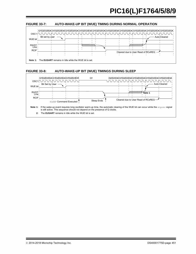
2014-2018 Microchip Technology Inc. DS40001775D-page 451
PIC16(L)F1764/5/8/9
FIGURE 33-7: AUTO-WAKE-UP BIT (WUE) TIMING DURING NORMAL OPERATION
FIGURE 33-8: AUTO-WAKE-UP BIT (WUE) TIMINGS DURING SLEEP
Q1 Q2 Q3 Q4 Q1 Q2 Q3 Q4 Q1 Q2 Q3 Q4 Q1 Q2 Q3 Q4 Q1 Q2 Q3 Q4 Q1 Q2 Q3 Q4 Q1 Q2 Q3 Q4 Q1 Q2 Q3 Q4 Q1 Q2 Q3 Q4 Q1 Q2 Q3 Q4
OSC1
WUE bit
RX/DT
RCIF
Bit set by user Auto-Cleared
Note 1: The EUSART remains in Idle while the WUE bit is set.
Line
Cleared due to User Read of RCxREG
Q1Q2 Q3 Q4 Q1Q2 Q3 Q4 Q1Q2 Q3 Q4 Q1 Q2 Q3 Q4 Q1Q2 Q3 Q4 Q1Q2 Q3 Q4 Q1 Q2 Q3 Q4 Q1Q2 Q3 Q4
OSC1
WUE bit
RX/DT
RCIF
SLEEP Command Executed
Note 1
Note 1: If the wake-up event requires long oscillator warm-up time, the automatic clearing of the WUE bit can occur while the stposc signalis still active. This sequence should not depend on the presence of Q clocks.
2: The EUSART remains in Idle while the WUE bit is set.
Sleep Ends
Auto-Cleared
Cleared due to User Read of RCxREG
Bit Set by User
Line

2014-2018 Microchip Technology Inc. DS40001775D-page 452
PIC16(L)F1764/5/8/9
33.4.4 BREAK CHARACTER SEQUENCE
The EUSART module has the capability of sending thespecial Break character sequences that are required bythe LIN bus standard. A Break character consists of aStart bit, followed by 12 ‘0’ bits and a Stop bit.
To send a Break character, set the SENDB and TXENbits of the TXxSTA register. The Break character trans-mission is then initiated by a write to the TXxREG. Thevalue of data written to TXxREG will be ignored and all‘0’s will be transmitted.
The SENDB bit is automatically reset by hardware afterthe corresponding Stop bit is sent. This allows the userto preload the transmit FIFO with the next transmit bytefollowing the Break character (typically, the Synccharacter in the LIN specification).
The TRMT bit of the TXxSTA register indicates when thetransmit operation is active or Idle, just as it does duringnormal transmission. See Figure 33-9 for the timing ofthe Break character sequence.
33.4.4.1 Break and Sync Transmit Sequence
The following sequence will start a message frameheader made up of a Break, followed by an auto-baudSync byte. This sequence is typical of a LIN bus master.
1. Configure the EUSART for the desired mode.
2. Set the TXEN and SENDB bits to enable theBreak sequence.
3. Load the TXxREG with a dummy character toinitiate transmission (the value is ignored).
4. Write ‘55h’ to TXxREG to load the Sync characterinto the transmit FIFO buffer.
5. After the Break has been sent, the SENDB bit isreset by hardware and the Sync character isthen transmitted.
When the TXxREG becomes empty, as indicated bythe TXIF, the next data byte can be written to TXxREG.
33.4.5 RECEIVING A BREAK CHARACTER
The Enhanced USART module can receive a Breakcharacter in two ways.
The first method to detect a Break character uses theFERR bit of the RCxSTA register and the received dataas indicated by RCxREG. The Baud Rate Generator isassumed to have been initialized to the expected baudrate.
A Break character has been received when;
• RCIF bit is set
• FERR bit is set
• RCxREG = 00h
The second method uses the auto-wake-up featuredescribed in Section 33.4.3 “Auto-Wake-up onBreak”. By enabling this feature, the EUSART willsample the next two transitions on RX/DT, cause anRCIF interrupt and receive the next data byte followedby another interrupt.
Note that following a Break character, the user willtypically want to enable the Auto-Baud Detect feature.For both methods, the user can set the ABDEN bit ofthe BAUDxCON register before placing the EUSART inSleep mode.
FIGURE 33-9: SEND BREAK CHARACTER SEQUENCE
Write to TXxREGDummy Write
BRG Output(Shift Clock)
Start bit bit 0 bit 1 bit 11 Stop bit
Break
TXIF bit(Transmit
Interrupt Flag)
TX (pin)
TRMT bit(Transmit Shift
Empty Flag)
SENDB(send Break
control bit)
SENDB Sampled Here Auto Cleared
2014-2018 Microchip Technology Inc. DS40001775D-page 453
PIC16(L)F1764/5/8/9
33.5 EUSART Synchronous Mode
Synchronous serial communications are typically usedin systems with a single master and one or moreslaves. The master device contains the necessarycircuitry for baud rate generation and supplies the clockfor all devices in the system. Slave devices can takeadvantage of the master clock by eliminating theinternal clock generation circuitry.
There are two signal lines in Synchronous mode: abidirectional data line and a clock line. Slaves use theexternal clock supplied by the master to shift the serialdata into and out of their respective receive and trans-mit shift registers. Since the data line is bidirectional,synchronous operation is half-duplex only. Half-duplexrefers to the fact that master and slave devices canreceive and transmit data, but not both simultaneously.The EUSART can operate as either a master or slavedevice.
Start and Stop bits are not used in synchronoustransmissions.
33.5.1 SYNCHRONOUS MASTER MODE
The following bits are used to configure the EUSARTfor synchronous master operation:
• SYNC = 1
• CSRC = 1
• SREN = 0 (for transmit); SREN = 1 (for receive)
• CREN = 0 (for transmit); CREN = 1 (for receive)
• SPEN = 1
Setting the SYNC bit of the TXxSTA register configuresthe device for synchronous operation. Setting the CSRCbit of the TXxSTA register configures the device as amaster. Clearing the SREN and CREN bits of theRCxSTA register ensures that the device is in theTransmit mode, otherwise the device will be configuredto receive. Setting the SPEN bit of the RCxSTA registerenables the EUSART.
33.5.1.1 Master Clock
Synchronous data transfers use a separate clock line,which is synchronous with the data. A device config-ured as a master transmits the clock on the TX/CK line.The TX/CK pin output driver is automatically enabledwhen the EUSART is configured for synchronoustransmit or receive operation. Serial data bits changeon the leading edge to ensure they are valid at thetrailing edge of each clock. One clock cycle is gener-ated for each data bit. Only as many clock cycles aregenerated as there are data bits.
33.5.1.2 Clock Polarity
A clock polarity option is provided for Microwirecompatibility. Clock polarity is selected with the SCKPbit of the BAUDxCON register. Setting the SCKP bitsets the clock Idle state as high. When the SCKP bit isset, the data changes on the falling edge of each clock.Clearing the SCKP bit sets the Idle state as low. Whenthe SCKP bit is cleared, the data changes on the risingedge of each clock.
33.5.1.3 Synchronous Master Transmission
Data is transferred out of the device on the RX/DT pin.The RX/DT and TX/CK pin output drivers are automat-ically enabled when the EUSART is configured forsynchronous master transmit operation.
A transmission is initiated by writing a character to theTXxREG register. If the TSR still contains all or part ofa previous character the new character data is held inthe TXxREG until the last bit of the previous characterhas been transmitted. If this is the first character, or theprevious character has been completely flushed fromthe TSR, the data in the TXxREG is immediately trans-ferred to the TSR. The transmission of the charactercommences immediately following the transfer of thedata to the TSR from the TXxREG.
Each data bit changes on the leading edge of themaster clock and remains valid until the subsequentleading clock edge.
33.5.1.4 Synchronous Master Transmission Setup
1. Initialize the SPxBRGH, SPxBRGL register pairand the BRGH and BRG16 bits to achieve thedesired baud rate (see Section 33.4 “EUSARTBaud Rate Generator (BRG)”).
2. Enable the synchronous master serial port bysetting bits, SYNC, SPEN and CSRC.
3. Disable Receive mode by clearing bits, SRENand CREN.
4. Enable Transmit mode by setting the TXEN bit.
5. If 9-bit transmission is desired, set the TX9 bit.
6. If interrupts are desired, set the TXIE bit of thePIE1 register, and the GIE and PEIE bits of theINTCON register.
7. If 9-bit transmission is selected, the ninth bitshould be loaded in the TX9D bit.
8. Start transmission by loading data to theTXxREG register.
Note: The TSR register is not mapped in datamemory, so it is not available to the user.

2014-2018 Microchip Technology Inc. DS40001775D-page 454
PIC16(L)F1764/5/8/9
FIGURE 33-10: SYNCHRONOUS TRANSMISSION
FIGURE 33-11: SYNCHRONOUS TRANSMISSION (THROUGH TXEN)
bit 0 bit 1 bit 7Word 1
bit 2 bit 0 bit 1 bit 7RX/DT
Write toTXxREG Reg
TXIF bit(Interrupt Flag)
TXEN bit ‘1’ ‘1’
Word 2
TRMT bit
Write Word 1 Write Word 2
Note: Sync Master mode, SPxBRGL = 0; continuous transmission of two 8-bit words.
PinTX/CK Pin
TX/CK Pin
(SCKP = 0)
(SCKP = 1)
RX/DT Pin
TX/CK Pin
Write toTXxREG Reg
TXIF bit
TRMT bit
bit 0 bit 1 bit 2 bit 6 bit 7
TXEN bit

2014-2018 Microchip Technology Inc. DS40001775D-page 455
PIC16(L)F1764/5/8/9
TABLE 33-7: SUMMARY OF REGISTERS ASSOCIATED WITH SYNCHRONOUS MASTER TRANSMISSION
Name Bit 7 Bit 6 Bit 5 Bit 4 Bit 3 Bit 2 Bit 1 Bit 0Register on Page
ANSELA — — — ANSA4 — ANSA<2:0> 137
ANSELB(1) ANSB<7:4> — — — — 143
ANSELC ANSC<7:6>(1) — — ANSC<3:0> 148
BAUD1CON ABDOVF RCIDL — SCKP BRG16 — WUE ABDEN 443
INTCON GIE PEIE TMR0IE INTE IOCIE TMR0IF INTF IOCIF 101
PIE1 TMR1GIE ADIE RCIE TXIE SSP1IE CCP1IE TMR2IE TMR1IE 102
PIR1 TMR1GIF ADIF RCIF TXIF SSP1IF CCP1IF TMR2IF TMR1IF 105
RC1STA SPEN RX9 SREN CREN ADDEN FERR OERR RX9D 442
RxyPPS — — — RxyPPS<4:0> 154
SP1BRGL BRG<7:0> 444
SP1BRGH BRG<15:8> 444
TRISA — — TRISA<5:4> —(2) TRISA<2:0> 136
TRISB(1) TRISB<7:4> — — — — 142
TRISC TRISC<7:6>(1) TRISC<5:0> 147
TX1REG EUSART Transmit Data Register 434*
TX1STA CSRC TX9 TXEN SYNC SENDB BRGH TRMT TX9D 441
Legend: — = unimplemented location, read as ‘0’. Shaded cells are not used for synchronous master transmission.
* Page provides register information.
Note 1: PIC16(L)F1768/9 only.
2: Unimplemented, read as ‘1’.

2014-2018 Microchip Technology Inc. DS40001775D-page 456
PIC16(L)F1764/5/8/9
33.5.1.5 Synchronous Master Reception
Data is received at the RX/DT pin. The RX/DT pinoutput driver is automatically disabled when theEUSART is configured for synchronous master receiveoperation.
In Synchronous mode, reception is enabled by settingeither the Single Receive Enable bit (SREN of theRCxSTA register) or the Continuous Receive Enablebit (CREN of the RCxSTA register).
When SREN is set and CREN is clear, only as manyclock cycles are generated as there are data bits in asingle character. The SREN bit is automatically clearedat the completion of one character. When CREN is set,clocks are continuously generated until CREN iscleared. If CREN is cleared in the middle of a character,the CK clock stops immediately and the partial charac-ter is discarded. If SREN and CREN are both set, thenSREN is cleared at the completion of the first characterand CREN takes precedence.
To initiate reception, set either SREN or CREN. Data issampled at the RX/DT pin on the trailing edge of theTX/CK clock pin and is shifted into the Receive ShiftRegister (RSR). When a complete character isreceived into the RSR, the RCIF bit is set and the char-acter is automatically transferred to the two-characterreceive FIFO. The Least Significant eight bits of the topcharacter in the receive FIFO are available in RCxREG.The RCIF bit remains set as long as there are unreadcharacters in the receive FIFO.
33.5.1.6 Slave Clock
Synchronous data transfers use a separate clock line,which is synchronous with the data. A device configuredas a slave receives the clock on the TX/CK line. TheTX/CK pin output driver is automatically disabled whenthe device is configured for synchronous slave transmitor receive operation. Serial data bits change on theleading edge to ensure they are valid at the trailing edgeof each clock. One data bit is transferred for each clockcycle. Only as many clock cycles should be received asthere are data bits.
33.5.1.7 Receive Overrun Error
The receive FIFO buffer can hold two characters. Anoverrun error will be generated if a third character, in itsentirety, is received before RCxREG is read to accessthe FIFO. When this happens, the OERR bit of theRCxSTA register is set. Previous data in the FIFO willnot be overwritten. The two characters in the FIFObuffer can be read, however, no additional characterswill be received until the error is cleared. The OERR bitcan only be cleared by clearing the overrun condition.If the overrun error occurred when the SREN bit is setand CREN is clear, then the error is cleared by readingRCxREG. If the overrun occurred when the CREN bit isset, then the error condition is cleared by either clearingthe CREN bit of the RCxSTA register or by clearing theSPEN bit which resets the EUSART.
33.5.1.8 Receiving 9-Bit Characters
The EUSART supports 9-bit character reception. Whenthe RX9 bit of the RCxSTA register is set the EUSARTwill shift nine bits into the RSR for each characterreceived. The RX9D bit of the RCxSTA register is theninth, and Most Significant, data bit of the top unreadcharacter in the receive FIFO. When reading 9-bit datafrom the receive FIFO buffer, the RX9D data bit mustbe read before reading the eight Least Significant bitsfrom the RCxREG.
33.5.1.9 Synchronous Master Reception Setup
1. Initialize the SPxBRGH, SPxBRGL register pairfor the appropriate baud rate. Set or clear theBRGH and BRG16 bits, as required, to achievethe desired baud rate.
2. Clear the ANSELx bit for the RX pin (if applicable).
3. Enable the synchronous master serial port bysetting bits, SYNC, SPEN and CSRC.
4. Ensure bits, CREN and SREN, are clear.
5. If interrupts are desired, set the RCIE bit of thePIE1 register, and the GIE and PEIE bits of theINTCON register.
6. If 9-bit reception is desired, set bit, RX9.
7. Start reception by setting the SREN bit, or forcontinuous reception, set the CREN bit.
8. Interrupt flag bit, RCIF, will be set when recep-tion of a character is complete. An interrupt willbe generated if the enable bit, RCIE, was set.
9. Read the RCxSTA register to get the ninth bit (ifenabled) and determine if any error occurredduring reception.
10. Read the 8-bit received data by reading theRCxREG register.
11. If an overrun error occurs, clear the error byeither clearing the CREN bit of the RCxSTAregister or by clearing the SPEN bit which resetsthe EUSART.
Note: If the RX/DT function is on an analog pin,the corresponding ANSELx bit must becleared for the receiver to function.
Note: If the device is configured as a slave andthe TX/CK function is on an analog pin, thecorresponding ANSELx bit must becleared.

2014-2018 Microchip Technology Inc. DS40001775D-page 457
PIC16(L)F1764/5/8/9
FIGURE 33-12: SYNCHRONOUS RECEPTION (MASTER MODE, SREN)
TABLE 33-8: SUMMARY OF REGISTERS ASSOCIATED WITH SYNCHRONOUS MASTER RECEPTION
Name Bit 7 Bit 6 Bit 5 Bit 4 Bit 3 Bit 2 Bit 1 Bit 0Register on Page
ANSELA — — — ANSA4 — ANSA<2:0> 137
ANSELB(1) ANSB<7:4> — — — — 143
ANSELC ANSC<7:6>(1) — — ANSC<3:0> 148
BAUD1CON ABDOVF RCIDL — SCKP BRG16 — WUE ABDEN 443
CKPPS — — — CKPPS<4:0> 154, 156
INTCON GIE PEIE TMR0IE INTE IOCIE TMR0IF INTF IOCIF 101
PIE1 TMR1GIE ADIE RCIE TXIE SSP1IE CCP1IE TMR2IE TMR1IE 102
PIR1 TMR1GIF ADIF RCIF TXIF SSP1IF CCP1IF TMR2IF TMR1IF 105
RC1REG EUSART Receive Data Register 437*
RC1STA SPEN RX9 SREN CREN ADDEN FERR OERR RX9D 442
RXPPS — — — RXPPS<4:0> 154, 156
RxyPPS — — — RxyPPS<4:0> 154
SP1BRGL BRG<7:0> 444*
SP1BRGH BRG<15:8> 444*
TRISA — — TRISA<5:4> —(2) TRISA<2:0> 136
TRISB(1) TRISB<7:4> — — — — 142
TRISC TRISC<7:6>(1) TRISC<5:0> 147
TX1STA CSRC TX9 TXEN SYNC SENDB BRGH TRMT TX9D 441
Legend: — = unimplemented location, read as ‘0’. Shaded cells are not used for synchronous master reception.
* Page provides register information.
Note 1: PIC16(L)F1768/9 only.
2: Unimplemented, read as ‘1’.
CREN bit
RX/DT
Write toSREN bit
SREN bit
RCIF bit(Interrupt)
ReadRCxREG
‘0’
bit 0 bit 1 bit 2 bit 3 bit 4 bit 5 bit 6 bit 7
‘0’
Note: Timing diagram demonstrates Sync Master mode with bit SREN = 1 and bit BRGH = 0.
TX/CK Pin
TX/CK Pin
Pin
(SCKP = 0)
(SCKP = 1)
2014-2018 Microchip Technology Inc. DS40001775D-page 458
PIC16(L)F1764/5/8/9
33.5.2 SYNCHRONOUS SLAVE MODE
The following bits are used to configure the EUSARTfor synchronous slave operation:
• SYNC = 1
• CSRC = 0
• SREN = 0 (for transmit); SREN = 1 (for receive)
• CREN = 0 (for transmit); CREN = 1 (for receive)
• SPEN = 1
Setting the SYNC bit of the TXxSTA register configuresthe device for synchronous operation. Clearing theCSRC bit of the TXxSTA register configures the device asa slave. Clearing the SREN and CREN bits of theRCxSTA register ensures that the device is in theTransmit mode, otherwise the device will be configured toreceive. Setting the SPEN bit of the RCxSTA registerenables the EUSART.
33.5.2.1 EUSART Synchronous Slave Transmit
The operation of the Synchronous Master and Slavemodes are identical (see Section 33.5.1.3“Synchronous Master Transmission”), except in thecase of Sleep mode.
If two words are written to the TXxREG and then theSLEEP instruction is executed, the following will occur:
1. The first character will immediately transfer tothe TSR register and transmit.
2. The second word will remain in the TXxREGregister.
3. The TXIF bit will not be set.
4. After the first character has been shifted out ofTSR, the TXxREG register will transfer thesecond character to the TSR and the TXIF bit willnow be set.
5. If the PEIE and TXIE bits are set, the interruptwill wake the device from Sleep and execute thenext instruction. If the GIE bit is also set, theprogram will call the Interrupt Service Routine.
33.5.2.2 Synchronous Slave Transmission Setup
1. Set the SYNC and SPEN bits, and clear theCSRC bit.
2. Clear the ANSEL bit for the CK pin (if applicable).
3. Clear the CREN and SREN bits.
4. If interrupts are desired, set the TXIE bit of thePIE1 register, and the GIE and PEIE bits of theINTCON register.
5. If 9-bit transmission is desired, set the TX9 bit.
6. Enable transmission by setting the TXEN bit.
7. If 9-bit transmission is selected, insert the MostSignificant bit into the TX9D bit.
8. Start transmission by writing the LeastSignificant eight bits to the TXxREG register.

2014-2018 Microchip Technology Inc. DS40001775D-page 459
PIC16(L)F1764/5/8/9
TABLE 33-9: SUMMARY OF REGISTERS ASSOCIATED WITH SYNCHRONOUS SLAVE TRANSMISSION
Name Bit 7 Bit 6 Bit 5 Bit 4 Bit 3 Bit 2 Bit 1 Bit 0Register on Page
ANSELA — — — ANSA4 — ANSA<2:0> 137
ANSELB(1) ANSB<7:4> — — — — 143
ANSELC ANSC<7:6>(1) — — ANSC<3:0> 148
BAUD1CON ABDOVF RCIDL — SCKP BRG16 — WUE ABDEN 443
CKPPS — — — CKPPS<4:0> 154, 156
INTCON GIE PEIE TMR0IE INTE IOCIE TMR0IF INTF IOCIF 101
PIE1 TMR1GIE ADIE RCIE TXIE SSP1IE CCP1IE TMR2IE TMR1IE 102
PIR1 TMR1GIF ADIF RCIF TXIF SSP1IF CCP1IF TMR2IF TMR1IF 105
RC1STA SPEN RX9 SREN CREN ADDEN FERR OERR RX9D 442
RXPPS — — — RXPPS<4:0> 154, 156
RxyPPS — — — RxyPPS<4:0> 154
TRISA — — TRISA<5:4> —(2) TRISA<2:0> 136
TRISB(1) TRISB<7:4> — — — — 142
TRISC TRISC<7:6>(1) TRISC<5:0> 147
TX1REG EUSART Transmit Data Register 434*
TX1STA CSRC TX9 TXEN SYNC SENDB BRGH TRMT TX9D 441
Legend: — = unimplemented location, read as ‘0’. Shaded cells are not used for synchronous slave transmission.
* Page provides register information.
Note 1: PIC16(L)F1768/9 only.
2: Unimplemented, read as ‘1’.

2014-2018 Microchip Technology Inc. DS40001775D-page 460
PIC16(L)F1764/5/8/9
33.5.2.3 EUSART Synchronous Slave Reception
The operation of the Synchronous Master and Slavemodes is identical (Section 33.5.1.5 “SynchronousMaster Reception”), with the following exceptions:
• Sleep
• CREN bit is always set, therefore the receiver is never Idle
• SREN bit, which is a “don’t care” in Slave mode
A character may be received while in Sleep mode bysetting the CREN bit prior to entering Sleep. Once theword is received, the RSR register will transfer the datato the RCxREG register. If the RCIE enable bit is set,the interrupt generated will wake the device from Sleepand execute the next instruction. If the GIE bit is alsoset, the program will branch to the interrupt vector.
33.5.2.4 Synchronous Slave Reception Setup
1. Set the SYNC and SPEN bits, and clear theCSRC bit.
2. Clear the ANSELx bit for both the CK and DTpins (if applicable).
3. If interrupts are desired, set the RCIE bit of thePIE1 register, and the GIE and PEIE bits of theINTCON register.
4. If 9-bit reception is desired, set the RX9 bit.
5. Set the CREN bit to enable reception.
6. The RCIF bit will be set when reception iscomplete. An interrupt will be generated if theRCIE bit was set.
7. If 9-bit mode is enabled, retrieve the MostSignificant bit from the RX9D bit of the RCxSTAregister.
8. Retrieve the eight Least Significant bits from thereceive FIFO by reading the RCxREG register.
9. If an overrun error occurs, clear the error byeither clearing the CREN bit of the RCxSTAregister or by clearing the SPEN bit which resetsthe EUSART.
TABLE 33-10: SUMMARY OF REGISTERS ASSOCIATED WITH SYNCHRONOUS SLAVE RECEPTION
Name Bit 7 Bit 6 Bit 5 Bit 4 Bit 3 Bit 2 Bit 1 Bit 0Register on Page
ANSELA — — — ANSA4 — ANSA<2:0> 137
ANSELB(1) ANSB<7:4> — — — — 143
ANSELC ANSC<7:6>(1) — — ANSC<3:0> 148
BAUD1CON ABDOVF RCIDL — SCKP BRG16 — WUE ABDEN 443
CKPPS — — — CKPPS<4:0> 154, 156
INTCON GIE PEIE TMR0IE INTE IOCIE TMR0IF INTF IOCIF 101
PIE1 TMR1GIE ADIE RCIE TXIE SSP1IE CCP1IE TMR2IE TMR1IE 102
PIR1 TMR1GIF ADIF RCIF TXIF SSP1IF CCP1IF TMR2IF TMR1IF 105
RC1REG EUSART Receive Data Register 437*
RC1STA SPEN RX9 SREN CREN ADDEN FERR OERR RX9D 442
RXPPS — — — RXPPS<4:0> 154, 156
TRISA — — TRISA<5:4> —(2) TRISA<2:0> 136
TRISB(1) TRISB<7:4> — — — — 142
TRISC TRISC<7:6>(1) TRISC<5:0> 147
TX1STA CSRC TX9 TXEN SYNC SENDB BRGH TRMT TX9D 441
Legend: — = unimplemented location, read as ‘0’. Shaded cells are not used for synchronous slave reception.
* Page provides register information.
Note 1: PIC16(L)F1768/9 only.
2: Unimplemented, read as ‘1’.

2014-2018 Microchip Technology Inc. DS40001775D-page 461
PIC16(L)F1764/5/8/9
33.6 EUSART Operation During Sleep
The EUSART will remain active during Sleep only in theSynchronous Slave mode. All other modes require thesystem clock and therefore, cannot generate thenecessary signals to run the Transmit or Receive Shiftregisters during Sleep.
Synchronous Slave mode uses an externally generatedclock to run the Transmit and Receive Shift registers.
33.6.1 SYNCHRONOUS RECEIVE DURING SLEEP
To receive during Sleep, all the following conditionsmust be met before entering Sleep mode:
• RCxSTA and TXxSTA Control registers must be configured for synchronous slave reception (see Section 33.5.2.4 “Synchronous Slave Reception Setup”).
• If interrupts are desired, set the RCIE bit of the PIE1 register, and the GIE and PEIE bits of the INTCON register.
• The RCIF interrupt flag must be cleared by read-ing RCxREG to unload any pending characters in the receive buffer.
Upon entering Sleep mode, the device will be ready toaccept data and clocks on the RX/DT and TX/CK pins,respectively. When the data word has been completelyclocked in by the external device, the RCIF interruptflag bit of the PIR1 register will be set; thereby, wakingthe processor from Sleep.
Upon waking from Sleep, the instruction following theSLEEP instruction will be executed. If the GlobalInterrupt Enable (GIE) bit of the INTCON register isalso set, then the Interrupt Service Routine at address,004h, will be called.
33.6.2 SYNCHRONOUS TRANSMIT DURING SLEEP
To transmit during Sleep, all the following conditionsmust be met before entering Sleep mode:
• The RCxSTA and TXxSTA Control registers must be configured for synchronous slave transmission (see Section 33.5.2.2 “Synchronous Slave Transmission Setup”).
• The TXIF interrupt flag must be cleared by writing the output data to the TXxREG; thereby, filling the TSR and transmit buffer.
• If interrupts are desired, set the TXIE bit of the PIE1 register and the PEIE bit of the INTCON register.
• Interrupt enable bits, TXIE of the PIE1 register and PEIE of the INTCON register, must set.
Upon entering Sleep mode, the device will be ready toaccept clocks on the TX/CK pin and transmit data onthe RX/DT pin. When the data word in the TSR hasbeen completely clocked out by the external device, thepending byte in the TXxREG will transfer to the TSRand the TXIF flag will be set; thereby, waking theprocessor from Sleep. At this point, the TXxREG isavailable to accept another character for transmission,which will clear the TXIF flag.
Upon waking from Sleep, the instruction following theSLEEP instruction will be executed. If the GlobalInterrupt Enable (GIE) bit is also set, then the InterruptService Routine at address, 0004h, will be called.

2014-2018 Microchip Technology Inc. DS40001775D-page 462
PIC16(L)F1764/5/8/9
34.0 IN-CIRCUIT SERIAL PROGRAMMING™ (ICSP™)
ICSP™ programming allows customers to manufacturecircuit boards with unprogrammed devices. Programmingcan be done after the assembly process, allowing thedevice to be programmed with the most recent firmwareor a custom firmware. Five pins are needed for ICSP™programming:
• ICSPCLK
• ICSPDAT
• MCLR/VPP
• VDD
• VSS
In Program/Verify mode, the program memory, UserIDs and the Configuration Words are programmedthrough serial communications. The ICSPDAT pin is abidirectional I/O used for transferring the serial dataand the ICSPCLK pin is the clock input. For moreinformation on ICSP™ refer to the “PIC16(L)F170XMemory Programming Specification” (DS40001683).
34.1 High-Voltage Programming Entry Mode
The device is placed into High-Voltage ProgrammingEntry mode by holding the ICSPCLK and ICSPDATpins low, then raising the voltage on MCLR/VPP to VIHH.
34.2 Low-Voltage Programming Entry Mode
The Low-Voltage Programming Entry mode allows thePIC® Flash MCUs to be programmed using VDD only,without high voltage. When the LVP bit of ConfigurationWords is set to ‘1’, the low-voltage ICSP programmingentry is enabled. To disable the Low-Voltage ICSPmode, the LVP bit must be programmed to ‘0’.
Entry into the Low-Voltage Programming Entry moderequires the following steps:
1. MCLR is brought to VIL.
2. A 32-bit key sequence is presented onICSPDAT, while clocking ICSPCLK.
Once the key sequence is complete, MCLR must beheld at VIL for as long as Program/Verify mode is to bemaintained.
If Low-Voltage Programming mode is enabled(LVP = 1), the MCLR Reset function is automaticallyenabled and cannot be disabled. See Section 6.5“MCLR” for more information.
The LVP bit can only be reprogrammed to ‘0’ by usingthe High-Voltage Programming mode.
34.3 Common Programming Interfaces
Connection to a target device is typically done throughan ICSP header. A commonly found connector ondevelopment tools is the RJ-11 in the 6P6C (6-pin,6-connector) configuration. See Figure 34-1.
FIGURE 34-1: ICD RJ-11 STYLE CONNECTOR INTERFACE
Another connector often found in use with the PICkit™programmers is a standard 6-pin header with 0.1 inchspacing. Refer to Figure 34-2.
For additional interface recommendations, refer to yourspecific device programmer manual prior to PCBdesign.
It is recommended that isolation devices be used toseparate the programming pins from other circuitry.The type of isolation is highly dependent on the specificapplication and may include devices, such as resistors,diodes or even jumpers. See Figure 34-3 for moreinformation.
1
2
3
4
5
6
Target
Bottom SidePC BoardVPP/MCLR VSS
ICSPCLKVDD
ICSPDATNC
Pin Description*
1 = VPP/MCLR
2 = VDD Target
3 = VSS (ground)
4 = ICSPDAT
5 = ICSPCLK
6 = No Connect

2014-2018 Microchip Technology Inc. DS40001775D-page 463
PIC16(L)F1764/5/8/9
FIGURE 34-2: PICkit™ PROGRAMMER STYLE CONNECTOR INTERFACE
FIGURE 34-3: TYPICAL CONNECTION FOR ICSP™ PROGRAMMING
123456
* The 6-pin header (0.100" spacing) accepts 0.025" square pins.
Pin Description*
1 = VPP/MCLR
2 = VDD Target
3 = VSS (ground)
4 = ICSPDAT
5 = ICSPCLK
6 = No Connect
Pin 1 Indicator
VDD
VPP
VSS
ExternalDevice to be
Data
Clock
VDD
MCLR/VPP
VSS
ICSPDAT
ICSPCLK
* **
To Normal Connections
* Isolation devices (as required).
Programming Signals Programmed
VDD

2014-2018 Microchip Technology Inc. DS40001775D-page 464
PIC16(L)F1764/5/8/9
35.0 INSTRUCTION SET SUMMARY
Each instruction is a 14-bit word containing the opera-tion code (opcode) and all required operands. Theopcodes are broken into three broad categories.
• Byte Oriented
• Bit Oriented
• Literal and Control
The literal and control category contains the mostvaried instruction word format.
Table 35-3 lists the instructions recognized by theMPASMTM assembler.
All instructions are executed within a single instructioncycle, with the following exceptions, which may taketwo or three cycles:
• Subroutine takes two cycles (CALL, CALLW)• Returns from interrupts or subroutines take two
cycles (RETURN, RETLW, RETFIE)• Program branching takes two cycles (GOTO, BRA, BRW, BTFSS, BTFSC, DECFSZ, INCSFZ)
• One additional instruction cycle will be used when any instruction references an indirect file register and the file select register is pointing to program memory.
One instruction cycle consists of four oscillator cycles;for an oscillator frequency of 4 MHz, this gives anominal instruction execution rate of 1 MHz.
All instruction examples use the format ‘0xhh’ torepresent a hexadecimal number, where ‘h’ signifies ahexadecimal digit.
35.1 Read-Modify-Write Operations
Any instruction that specifies a file register as part ofthe instruction performs a Read-Modify-Write (R-M-W)operation. The register is read, the data is modified andthe result is stored according to either the instruction orthe destination designator, ‘d’. A read operation isperformed on a register even if the instruction writes tothat register.
TABLE 35-1: OPCODE FIELD DESCRIPTIONS
TABLE 35-2: ABBREVIATION DESCRIPTIONS
Field Description
f Register file address (0x00 to 0x7F).
W Working register (accumulator).
b Bit address within an 8-bit file register.
k Literal field, constant data or label
x Don’t care location (= 0 or 1). The assembler will generate code with x = 0. It is the recommended form of use for compatibility with all Microchip software tools.
d Destination select; d = 0: store result in W,d = 1: store result in file register f. Default is d = 1.
n FSR or INDF number (0-1).
mm Pre/Post-Increment/Decrement mode selection.
Field Description
PC Program Counter
TO Time-out bit
C Carry bit
DC Digit Carry bit
Z Zero bit
PD Power-Down bit

2014-2018 Microchip Technology Inc. DS40001775D-page 465
PIC16(L)F1764/5/8/9
FIGURE 35-1: GENERAL FORMAT FOR INSTRUCTIONS
Byte-oriented file register operations13 8 7 6 0
d = 0 for destination W
OPCODE d f (FILE #)
d = 1 for destination ff = 7-bit file register address
Bit-oriented file register operations13 10 9 7 6 0
OPCODE b (BIT #) f (FILE #)
b = 3-bit bit addressf = 7-bit file register address
Literal and control operations
13 8 7 0
OPCODE k (literal)
k = 8-bit immediate value
13 11 10 0
OPCODE k (literal)
k = 11-bit immediate value
General
CALL and GOTO instructions only
MOVLP instruction only
13 5 4 0
OPCODE k (literal)
k = 5-bit immediate value
MOVLB instruction only
13 9 8 0
OPCODE k (literal)
k = 9-bit immediate value
BRA instruction only
FSR Offset instructions
13 7 6 5 0
OPCODE n k (literal)
n = appropriate FSR
FSR Increment instructions
13 7 6 0
OPCODE k (literal)
k = 7-bit immediate value
13 3 2 1 0
OPCODE n m (mode)
n = appropriate FSRm = 2-bit mode value
k = 6-bit immediate value
13 0
OPCODE
OPCODE only

2014-2018 Microchip Technology Inc. DS40001775D-page 466
PIC16(L)F1764/5/8/9
TABLE 35-3: PIC16(L)F1764/5/8/9 INSTRUCTION SET
Mnemonic,Operands
Description Cycles14-Bit Opcode Status
AffectedNotes
MSb LSb
BYTE-ORIENTED FILE REGISTER OPERATIONS
ADDWFADDWFCANDWFASRFLSLFLSRFCLRFCLRWCOMFDECFINCFIORWFMOVFMOVWFRLFRRFSUBWFSUBWFBSWAPFXORWF
f, df, df, df, df, df, df–f, df, df, df, df, dff, df, df, df, df, df, d
Add W and fAdd with Carry W and fAND W with fArithmetic Right ShiftLogical Left ShiftLogical Right ShiftClear fClear WComplement fDecrement fIncrement fInclusive OR W with fMove fMove W to fRotate Left f through CarryRotate Right f through CarrySubtract W from fSubtract with Borrow W from fSwap nibbles in fExclusive OR W with f
11111111111111111111
0011001111110000000000000000000000110000
01111101010101110101011000010001100100111010010010000000110111000010101111100110
dfffdfffdfffdfffdfffdffflfff0000dfffdfffdfffdfffdfff1fffdfffdfffdfffdfffdfffdfff
ffffffffffffffffffffffffffff00xxffffffffffffffffffffffffffffffffffffffffffffffff
C, DC, ZC, DC, ZZC, ZC, ZC, ZZZZZZZZ
CCC, DC, ZC, DC, Z
Z
2222222
222222222222
BYTE ORIENTED SKIP OPERATIONS
DECFSZINCFSZ
f, df, d
Decrement f, Skip if 0Increment f, Skip if 0
1(2)1(2)
0000
10111111
dfffdfff
ffffffff
1, 21, 2
BIT-ORIENTED FILE REGISTER OPERATIONS
BCFBSF
f, bf, b
Bit Clear fBit Set f
11
0101
00bb01bb
bfffbfff
ffffffff
22
BIT-ORIENTED SKIP OPERATIONS
BTFSCBTFSS
f, bf, b
Bit Test f, Skip if ClearBit Test f, Skip if Set
1 (2)1 (2)
0101
10bb11bb
bfff bfff
ffffffff
1, 21, 2
LITERAL OPERATIONS
ADDLWANDLWIORLWMOVLBMOVLPMOVLWSUBLWXORLW
kkkkkkkk
Add literal and WAND literal with WInclusive OR literal with WMove literal to BSRMove literal to PCLATHMove literal to WSubtract W from literalExclusive OR literal with W
11111111
1111110011111111
11101001100000000001000011001010
kkkkkkkkkkkk001k1kkkkkkkkkkkkkkk
kkkkkkkkkkkkkkkkkkkkkkkkkkkkkkkk
C, DC, ZZZ
C, DC, ZZ
Note 1: If the Program Counter (PC) is modified, or a conditional test is true, the instruction requires two cycles. The second cycle is executed as a NOP.
2: If this instruction addresses an INDFn register and the MSb of the corresponding FSRn is set, this instruction will require one additional instruction cycle.
3: See Table 35-3 for the MOVIW and MOVWI instruction descriptions.

2014-2018 Microchip Technology Inc. DS40001775D-page 467
PIC16(L)F1764/5/8/9
TABLE 35-3: PIC16(L)F1764/5/8/9 INSTRUCTION SET (CONTINUED)
Mnemonic,Operands
Description Cycles14-Bit Opcode Status
AffectedNotes
MSb LSb
CONTROL OPERATIONS
BRABRWCALLCALLWGOTORETFIERETLWRETURN
k–k–kkk–
Relative BranchRelative Branch with WCall SubroutineCall Subroutine with WGo to addressReturn from interruptReturn with literal in WReturn from Subroutine
22222222
1100100010001100
001k00000kkk00001kkk000001000000
kkkk0000kkkk0000kkkk0000kkkk0000
kkkk1011kkkk1010kkkk1001kkkk1000
INHERENT OPERATIONS
CLRWDTNOPOPTIONRESETSLEEPTRIS
–––––f
Clear Watchdog TimerNo OperationLoad OPTION_REG register with WSoftware device ResetGo into Standby modeLoad TRIS register with W
111111
000000000000
000000000000000000000000
011000000110000001100110
010000000010000100110fff
TO, PD
TO, PD
C-COMPILER OPTIMIZED
ADDFSRMOVIW
MOVWI
n, kn mm
k[n]n mm
k[n]
Add Literal k to FSRnMove Indirect FSRn to W with pre/post inc/dec modifier, mmMove INDFn to W, Indexed Indirect.Move W to Indirect FSRn with pre/post inc/dec modifier, mmMove W to INDFn, Indexed Indirect.
11
11
1
1100
1100
11
00010000
11110000
1111
0nkk0001
0nkk0001
1nkk
kkkk0nmm
kkkk1nmm
kkkk
Z
Z
2, 3
22, 3
2
Note 1: If the Program Counter (PC) is modified, or a conditional test is true, the instruction requires two cycles. The second cycle is executed as a NOP.
2: If this instruction addresses an INDFn register and the MSb of the corresponding FSRn is set, this instruction will require one additional instruction cycle.
3: See Table 35-3 for the MOVIW and MOVWI instruction descriptions.

2014-2018 Microchip Technology Inc. DS40001775D-page 468
PIC16(L)F1764/5/8/9
35.2 Instruction Descriptions
ADDFSR Add Literal to FSRn
Syntax: [ label ] ADDFSR FSRn, k
Operands: -32 k 31n [ 0, 1]
Operation: FSR(n) + k FSR(n)
Status Affected: None
Description: The signed 6-bit literal ‘k’ is added to the contents of the FSRnH:FSRnL register pair.
FSRn is limited to the range 0000h-FFFFh. Moving beyond these bounds will cause the FSRn to wrap around.
ADDLW Add literal and W
Syntax: [ label ] ADDLW k
Operands: 0 k 255
Operation: (W) + k (W)
Status Affected: C, DC, Z
Description: The contents of the W register are added to the 8-bit literal ‘k’ and the result is placed in the W register.
ADDWF Add W and f
Syntax: [ label ] ADDWF f,d
Operands: 0 f 127d 0,1
Operation: (W) + (f) (destination)
Status Affected: C, DC, Z
Description: Add the contents of the W register with register ‘f’. If ‘d’ is ‘0’, the result is stored in the W register. If ‘d’ is ‘1’, the result is stored back in register ‘f’.
ADDWFC ADD W and CARRY bit to f
Syntax: [ label ] ADDWFC f {,d}
Operands: 0 f 127d [0,1]
Operation: (W) + (f) + (C) dest
Status Affected: C, DC, Z
Description: Add W, the Carry flag and data mem-ory location ‘f’. If ‘d’ is ‘0’, the result is placed in W. If ‘d’ is ‘1’, the result is placed in data memory location ‘f’.
ANDLW AND literal with W
Syntax: [ label ] ANDLW k
Operands: 0 k 255
Operation: (W) .AND. (k) (W)
Status Affected: Z
Description: The contents of W register are AND’ed with the 8-bit literal ‘k’. The result is placed in the W register.
ANDWF AND W with f
Syntax: [ label ] ANDWF f,d
Operands: 0 f 127d 0,1
Operation: (W) .AND. (f) (destination)
Status Affected: Z
Description: AND the W register with register ‘f’. If ‘d’ is ‘0’, the result is stored in the W register. If ‘d’ is ‘1’, the result is stored back in register ‘f’.
ASRF Arithmetic Right Shift
Syntax: [ label ] ASRF f {,d}
Operands: 0 f 127d [0,1]
Operation: (f<7>) dest<7>(f<7:1>) dest<6:0>,(f<0>) C,
Status Affected: C, Z
Description: The contents of register ‘f’ are shifted one bit to the right through the Carry flag. The MSb remains unchanged. If ‘d’ is ‘0’, the result is placed in W. If ‘d’ is ‘1’, the result is stored back in register ‘f’.
register f C

2014-2018 Microchip Technology Inc. DS40001775D-page 469
PIC16(L)F1764/5/8/9
BCF Bit Clear f
Syntax: [ label ] BCF f,b
Operands: 0 f 1270 b 7
Operation: 0 (f<b>)
Status Affected: None
Description: Bit ‘b’ in register ‘f’ is cleared.
BRA Relative Branch
Syntax: [ label ] BRA label [ label ] BRA $+k
Operands: -256 label - PC + 1 255-256 k 255
Operation: (PC) + 1 + k PC
Status Affected: None
Description: Add the signed 9-bit literal ‘k’ to the PC. Since the PC will have incremented to fetch the next instruction, the new address will be PC + 1 + k. This instruction is a 2-cycle instruction. This branch has a limited range.
BRW Relative Branch with W
Syntax: [ label ] BRW
Operands: None
Operation: (PC) + (W) PC
Status Affected: None
Description: Add the contents of W (unsigned) to the PC. Since the PC will have incremented to fetch the next instruction, the new address will be PC + 1 + (W). This instruction is a 2-cycle instruction.
BSF Bit Set f
Syntax: [ label ] BSF f,b
Operands: 0 f 1270 b 7
Operation: 1 (f<b>)
Status Affected: None
Description: Bit ‘b’ in register ‘f’ is set.
BTFSC Bit Test f, Skip if Clear
Syntax: [ label ] BTFSC f,b
Operands: 0 f 1270 b 7
Operation: skip if (f<b>) = 0
Status Affected: None
Description: If bit ‘b’ in register ‘f’ is ‘1’, the next instruction is executed.If bit ‘b’, in register ‘f’, is ‘0’, the next instruction is discarded, and a NOP is executed instead, making this a 2-cycle instruction.
BTFSS Bit Test f, Skip if Set
Syntax: [ label ] BTFSS f,b
Operands: 0 f 1270 b < 7
Operation: skip if (f<b>) = 1
Status Affected: None
Description: If bit ‘b’ in register ‘f’ is ‘0’, the next instruction is executed.If bit ‘b’ is ‘1’, then the next instruction is discarded and a NOP is executed instead, making this a 2-cycle instruction.

2014-2018 Microchip Technology Inc. DS40001775D-page 470
PIC16(L)F1764/5/8/9
CALL Call Subroutine
Syntax: [ label ] CALL k
Operands: 0 k 2047
Operation: (PC)+ 1 TOS,k PC<10:0>,(PCLATH<6:3>) PC<14:11>
Status Affected: None
Description: Call Subroutine. First, return address (PC + 1) is pushed onto the stack. The 11-bit immediate address is loaded into PC bits<10:0>. The upper bits of the PC are loaded from PCLATH. CALL is a 2-cycle instruction.
CALLW Subroutine Call With W
Syntax: [ label ] CALLW
Operands: None
Operation: (PC) +1 TOS,(W) PC<7:0>,(PCLATH<6:0>) PC<14:8>
Status Affected: None
Description: Subroutine call with W. First, the return address (PC + 1) is pushed onto the return stack. Then, the contents of W are loaded into PC<7:0>, and the contents of PCLATH into PC<14:8>. CALLW is a 2-cycle instruction.
CLRF Clear f
Syntax: [ label ] CLRF f
Operands: 0 f 127
Operation: 00h (f)1 Z
Status Affected: Z
Description: The contents of register ‘f’ are cleared and the Z bit is set.
CLRW Clear W
Syntax: [ label ] CLRW
Operands: None
Operation: 00h (W)1 Z
Status Affected: Z
Description: W register is cleared. Zero bit (Z) is set.
CLRWDT Clear Watchdog Timer
Syntax: [ label ] CLRWDT
Operands: None
Operation: 00h WDT0 WDT prescaler,1 TO1 PD
Status Affected: TO, PD
Description: CLRWDT instruction resets the Watch-dog Timer. It also resets the prescaler of the WDT. Status bits TO and PD are set.
COMF Complement f
Syntax: [ label ] COMF f,d
Operands: 0 f 127d [0,1]
Operation: (f) (destination)
Status Affected: Z
Description: The contents of register ‘f’ are complemented. If ‘d’ is ‘0’, the result is stored in W. If ‘d’ is ‘1’, the result is stored back in register ‘f’.
DECF Decrement f
Syntax: [ label ] DECF f,d
Operands: 0 f 127d [0,1]
Operation: (f) - 1 (destination)
Status Affected: Z
Description: Decrement register ‘f’. If ‘d’ is ‘0’, the result is stored in the W register. If ‘d’ is ‘1’, the result is stored back in register ‘f’.

2014-2018 Microchip Technology Inc. DS40001775D-page 471
PIC16(L)F1764/5/8/9
DECFSZ Decrement f, Skip if 0
Syntax: [ label ] DECFSZ f,d
Operands: 0 f 127d [0,1]
Operation: (f) - 1 (destination); skip if result = 0
Status Affected: None
Description: The contents of register ‘f’ are decre-mented. If ‘d’ is ‘0’, the result is placed in the W register. If ‘d’ is ‘1’, the result is placed back in register ‘f’. If the result is ‘1’, the next instruction is executed. If the result is ‘0’, then a NOP is executed instead, making it a 2-cycle instruction.
GOTO Unconditional Branch
Syntax: [ label ] GOTO k
Operands: 0 k 2047
Operation: k PC<10:0>PCLATH<6:3> PC<14:11>
Status Affected: None
Description: GOTO is an unconditional branch. The 11-bit immediate value is loaded into PC bits <10:0>. The upper bits of PC are loaded from PCLATH<4:3>. GOTO is a 2-cycle instruction.
INCF Increment f
Syntax: [ label ] INCF f,d
Operands: 0 f 127d [0,1]
Operation: (f) + 1 (destination)
Status Affected: Z
Description: The contents of register ‘f’ are incre-mented. If ‘d’ is ‘0’, the result is placed in the W register. If ‘d’ is ‘1’, the result is placed back in register ‘f’.
INCFSZ Increment f, Skip if 0
Syntax: [ label ] INCFSZ f,d
Operands: 0 f 127d [0,1]
Operation: (f) + 1 (destination), skip if result = 0
Status Affected: None
Description: The contents of register ‘f’ are incre-mented. If ‘d’ is ‘0’, the result is placed in the W register. If ‘d’ is ‘1’, the result is placed back in register ‘f’.If the result is ‘1’, the next instruction is executed. If the result is ‘0’, a NOP is executed instead, making it a 2-cycle instruction.
IORLW Inclusive OR literal with W
Syntax: [ label ] IORLW k
Operands: 0 k 255
Operation: (W) .OR. k (W)
Status Affected: Z
Description: The contents of the W register are OR’ed with the 8-bit literal ‘k’. The result is placed in the W register.
IORWF Inclusive OR W with f
Syntax: [ label ] IORWF f,d
Operands: 0 f 127d [0,1]
Operation: (W) .OR. (f) (destination)
Status Affected: Z
Description: Inclusive OR the W register with regis-ter ‘f’. If ‘d’ is ‘0’, the result is placed in the W register. If ‘d’ is ‘1’, the result is placed back in register ‘f’.

2014-2018 Microchip Technology Inc. DS40001775D-page 472
PIC16(L)F1764/5/8/9
LSLF Logical Left Shift
Syntax: [ label ] LSLF f {,d}
Operands: 0 f 127d [0,1]
Operation: (f<7>) C(f<6:0>) dest<7:1>0 dest<0>
Status Affected: C, Z
Description: The contents of register ‘f’ are shifted one bit to the left through the Carry flag. A ‘0’ is shifted into the LSb. If ‘d’ is ‘0’, the result is placed in W. If ‘d’ is ‘1’, the result is stored back in register ‘f’.
LSRF Logical Right Shift
Syntax: [ label ] LSRF f {,d}
Operands: 0 f 127d [0,1]
Operation: 0 dest<7>(f<7:1>) dest<6:0>,(f<0>) C,
Status Affected: C, Z
Description: The contents of register ‘f’ are shifted one bit to the right through the Carry flag. A ‘0’ is shifted into the MSb. If ‘d’ is ‘0’, the result is placed in W. If ‘d’ is ‘1’, the result is stored back in register ‘f’.
register f 0C
register f C0
MOVF Move f
Syntax: [ label ] MOVF f,d
Operands: 0 f 127d [0,1]
Operation: (f) (dest)
Status Affected: Z
Description: The contents of register f are moved to a destination dependent upon the status of d. If d = 0, destination is W register. If d = 1, the destination is file register f itself. d = 1 is useful to test a file register since status flag Z is affected.
Words: 1
Cycles: 1
Example: MOVF FSR, 0
After InstructionW = value in FSRn registerZ = 1

2014-2018 Microchip Technology Inc. DS40001775D-page 473
PIC16(L)F1764/5/8/9
MOVIW Move INDFn to W
Syntax: [ label ] MOVIW ++FSRn[ label ] MOVIW --FSRn[ label ] MOVIW FSRn++[ label ] MOVIW FSRn--[ label ] MOVIW k[FSRn]
Operands: n [0,1]mm [00,01, 10, 11]-32 k 31
Operation: INDFn WEffective address is determined by• FSRn + 1 (preincrement)• FSRn – 1 (predecrement)• FSRn + k (relative offset)After the Move, the FSRn value will be either:• FSRn + 1 (all increments)• FSRn – 1 (all decrements)• Unchanged
Status Affected: Z
Mode Syntax mm
Preincrement ++FSRn 00
Predecrement --FSRn 01
Postincrement FSRn++ 10
Postdecrement FSRn-- 11
Description: This instruction is used to move data between W and one of the indirect registers (INDFn). Before/after this move, the pointer (FSRn) is updated by pre/post incrementing/decrementing it.
Note: The INDFn registers are not physical registers. Any instruction that accesses an INDFn register actually accesses the register at the address specified by the FSRn.
FSRn is limited to the range 0000h-FFFFh. Incrementing/decrementing it beyond these bounds will cause it to wrap around.
MOVLB Move literal to BSR
Syntax: [ label ] MOVLB k
Operands: 0 k 31
Operation: k BSR
Status Affected: None
Description: The 5-bit literal ‘k’ is loaded into the Bank Select Register (BSR).
MOVLP Move literal to PCLATH
Syntax: [ label ] MOVLP k
Operands: 0 k 127
Operation: k PCLATH
Status Affected: None
Description: The 7-bit literal ‘k’ is loaded into the PCLATH register.
MOVLW Move literal to W
Syntax: [ label ] MOVLW k
Operands: 0 k 255
Operation: k (W)
Status Affected: None
Description: The 8-bit literal ‘k’ is loaded into W reg-ister. The “don’t cares” will assemble as ‘0’s.
Words: 1
Cycles: 1
Example: MOVLW 0x5A
After InstructionW = 0x5A
MOVWF Move W to f
Syntax: [ label ] MOVWF f
Operands: 0 f 127
Operation: (W) (f)
Status Affected: None
Description: Move data from W register to register ‘f’.
Words: 1
Cycles: 1
Example: MOVWF OPTION_REG
Before InstructionOPTION_REG = 0xFF
W = 0x4FAfter Instruction
OPTION_REG = 0x4F W = 0x4F

2014-2018 Microchip Technology Inc. DS40001775D-page 474
PIC16(L)F1764/5/8/9
MOVWI Move W to INDFn
Syntax: [ label ] MOVWI ++FSRn[ label ] MOVWI --FSRn[ label ] MOVWI FSRn++[ label ] MOVWI FSRn--[ label ] MOVWI k[FSRn]
Operands: n [0,1]mm [00,01, 10, 11]-32 k 31
Operation: W INDFnEffective address is determined by• FSRn + 1 (preincrement)• FSRn – 1 (predecrement)• FSRn + k (relative offset)After the Move, the FSRn value will be either:• FSRn + 1 (all increments)• FSRn – 1 (all decrements)Unchanged
Status Affected: None
Mode Syntax mm
Preincrement ++FSRn 00
Predecrement --FSRn 01
Postincrement FSRn++ 10
Postdecrement FSRn-- 11
Description: This instruction is used to move data between W and one of the indirect registers (INDFn). Before/after this move, the pointer (FSRn) is updated by pre/post incrementing/decrementing it.
Note: The INDFn registers are not physical registers. Any instruction that accesses an INDFn register actually accesses the register at the address specified by the FSRn.
FSRn is limited to the range 0000h-FFFFh. Incrementing/decrementing it beyond these bounds will cause it to wrap-around.
The increment/decrement operation on FSRn WILL NOT affect any Status bits.
NOP No Operation
Syntax: [ label ] NOP
Operands: None
Operation: No operation
Status Affected: None
Description: No operation.
Words: 1
Cycles: 1
Example: NOP
OPTIONLoad OPTION_REG Register with W
Syntax: [ label ] OPTION
Operands: None
Operation: (W) OPTION_REG
Status Affected: None
Description: Move data from W register to OPTION_REG register.
Words: 1
Cycles: 1
Example: OPTION
Before InstructionOPTION_REG = 0xFF
W = 0x4FAfter Instruction
OPTION_REG = 0x4F W = 0x4F
RESET Software Reset
Syntax: [ label ] RESET
Operands: None
Operation: Execute a device Reset. Resets the RI flag of the PCON register.
Status Affected: None
Description: This instruction provides a way to execute a hardware Reset by software.

2014-2018 Microchip Technology Inc. DS40001775D-page 475
PIC16(L)F1764/5/8/9
RETFIE Return from Interrupt
Syntax: [ label ] RETFIE k
Operands: None
Operation: TOS PC,1 GIE
Status Affected: None
Description: Return from Interrupt. Stack is POPed and Top-of-Stack (TOS) is loaded in the PC. Interrupts are enabled by setting Global Interrupt Enable bit, GIE (INTCON<7>). This is a 2-cycle instruction.
Words: 1
Cycles: 2
Example: RETFIE
After InterruptPC = TOSGIE = 1
RETLW Return with literal in W
Syntax: [ label ] RETLW k
Operands: 0 k 255
Operation: k (W); TOS PC
Status Affected: None
Description: The W register is loaded with the 8-bit literal ‘k’. The Program Counter is loaded from the top of the stack (the return address). This is a 2-cycle instruction.
Words: 1
Cycles: 2
Example:
TABLE
CALL TABLE;W contains table;offset value
• ;W now has table value••ADDWF PC ;W = offsetRETLW k1 ;Begin tableRETLW k2 ;•••RETLW kn ; End of table
Before InstructionW = 0x07
After InstructionW = value of k8
RETURN Return from Subroutine
Syntax: [ label ] RETURN
Operands: None
Operation: TOS PC
Status Affected: None
Description: Return from subroutine. The stack is POPed and the top of the stack (TOS) is loaded into the Program Counter. This is a 2-cycle instruction.
RLF Rotate Left f through Carry
Syntax: [ label ] RLF f,d
Operands: 0 f 127d [0,1]
Operation: See description below
Status Affected: C
Description: The contents of register ‘f’ are rotated one bit to the left through the Carry flag. If ‘d’ is ‘0’, the result is placed in the W register. If ‘d’ is ‘1’, the result is stored back in register ‘f’.
Words: 1
Cycles: 1
Example: RLF REG1,0
Before InstructionREG1 = 1110 0110C = 0
After InstructionREG1 = 1110 0110W = 1100 1100C = 1
Register fC

2014-2018 Microchip Technology Inc. DS40001775D-page 476
PIC16(L)F1764/5/8/9
RRF Rotate Right f through Carry
Syntax: [ label ] RRF f,d
Operands: 0 f 127d [0,1]
Operation: See description below
Status Affected: C
Description: The contents of register ‘f’ are rotated one bit to the right through the Carry flag. If ‘d’ is ‘0’, the result is placed in the W register. If ‘d’ is ‘1’, the result is placed back in register ‘f’.
SLEEP Enter Sleep mode
Syntax: [ label ] SLEEP
Operands: None
Operation: 00h WDT,0 WDT prescaler,1 TO,0 PD
Status Affected: TO, PD
Description: The Power-Down Status bit, PD, is cleared. Time-out Status bit, TO, is set. Watchdog Timer and its prescaler are cleared.The processor is put into Sleep mode with the oscillator stopped.
Register fC
SUBLW Subtract W from literal
Syntax: [ label ] SUBLW k
Operands: 0 k 255
Operation: k - (W) W)
Status Affected: C, DC, Z
Description: The W register is subtracted (2’s complement method) from the 8-bit literal ‘k’. The result is placed in the W register.
SUBWF Subtract W from f
Syntax: [ label ] SUBWF f,d
Operands: 0 f 127d [0,1]
Operation: (f) - (W) destination)
Status Affected: C, DC, Z
Description: Subtract (2’s complement method) W register from register ‘f’. If ‘d’ is ‘0’, the result is stored in the W register. If ‘d’ is ‘1’, the result is stored back in register ‘f.
SUBWFB Subtract W from f with Borrow
Syntax: SUBWFB f {,d}
Operands: 0 f 127d [0,1]
Operation: (f) – (W) – (B) dest
Status Affected: C, DC, Z
Description: Subtract W and the Borrow flag (Carry) from register ‘f’ (2’s complement method). If ‘d’ is ‘0’, the result is stored in W. If ‘d’ is ‘1’, the result is stored back in register ‘f’.
C = 0 W k
C = 1 W k
DC = 0 W<3:0> k<3:0>
DC = 1 W<3:0> k<3:0>
C = 0 W f
C = 1 W f
DC = 0 W<3:0> f<3:0>
DC = 1 W<3:0> f<3:0>

2014-2018 Microchip Technology Inc. DS40001775D-page 477
PIC16(L)F1764/5/8/9
SWAPF Swap Nibbles in f
Syntax: [ label ] SWAPF f,d
Operands: 0 f 127d [0,1]
Operation: (f<3:0>) (destination<7:4>),(f<7:4>) (destination<3:0>)
Status Affected: None
Description: The upper and lower nibbles of register ‘f’ are exchanged. If ‘d’ is ‘0’, the result is placed in the W register. If ‘d’ is ‘1’, the result is placed in register ‘f’.
TRIS Load TRIS Register with W
Syntax: [ label ] TRIS f
Operands: 5 f 7
Operation: (W) TRIS register ‘f’
Status Affected: None
Description: Move data from W register to TRIS register.When ‘f’ = 5, TRISA is loaded.When ‘f’ = 6, TRISB is loaded.When ‘f’ = 7, TRISC is loaded.
XORLW Exclusive OR literal with W
Syntax: [ label ] XORLW k
Operands: 0 k 255
Operation: (W) .XOR. k W)
Status Affected: Z
Description: The contents of the W register are XOR’ed with the 8-bit literal ‘k’. The result is placed in the W register.
XORWF Exclusive OR W with f
Syntax: [ label ] XORWF f,d
Operands: 0 f 127d [0,1]
Operation: (W) .XOR. (f) destination)
Status Affected: Z
Description: Exclusive OR the contents of the W register with register ‘f’. If ‘d’ is ‘0’, the result is stored in the W register. If ‘d’ is ‘1’, the result is stored back in register ‘f’.
2014-2018 Microchip Technology Inc. DS40001775D-page 478
PIC16(L)F1764/5/8/9
36.0 ELECTRICAL SPECIFICATIONS
36.1 Absolute Maximum Ratings(†)
Ambient temperature under bias............................................................................................................ -40°C to +125°C
Storage temperature .............................................................................................................................. -65°C to +150°C
Voltage on pins with respect to VSS
on VDD pin
PIC16F1764/5/8/9 ........................................................................................................... -0.3V to +6.5V
PIC16LF1764/5/8/9 ......................................................................................................... -0.3V to +4.0V
on MCLR pin ................................................................................................................................. -0.3V to +9.0V
on all other pins .................................................................................................................. -0.3V to (VDD + 0.3V)
Maximum current
on VSS pin(1)
-40°C TA +85°C .................................................................................................................... 250 mA
+85°C TA +125°C ................................................................................................................... 85 mA
on VDD pin(1)
-40°C TA +85°C .................................................................................................................... 250 mA
+85°C TA +125°C ................................................................................................................... 85 mA
Sunk by any standard I/O pin ..................................................................................................................... 50 mA
Sourced by any standard I/O pin ................................................................................................................ 50 mA
Sunk by any high-current I/O pin .............................................................................................................. 100 mA
Sourced by any high-current I/O pin ......................................................................................................... 100 mA
Sourced by any op amp output pin ........................................................................................................... 100 mA
Clamp current, IK (VPIN < 0 or VPIN > VDD) ......................................................................................................... 20 mA
Total power dissipation(2) .....................................................................................................................................800 mW
Note 1: Maximum current rating requires even load distribution across I/O pins. Maximum current rating may be limited by the device package power dissipation characterizations, see Table 36-6: Thermal Characteristics to calculate device specifications.
2: Power dissipation is calculated as follows: PDIS = VDD x {IDD – IOH} + {(VDD – VOH) x IOH} + (VOl x IOL).
† NOTICE: Stresses above those listed under “Absolute Maximum Ratings” may cause permanent damage to thedevice. This is a stress rating only and functional operation of the device at those or any other conditions above thoseindicated in the operation listings of this specification is not implied. Exposure above maximum rating conditions forextended periods may affect device reliability.

2014-2018 Microchip Technology Inc. DS40001775D-page 479
PIC16(L)F1764/5/8/9
36.2 Standard Operating Conditions
The standard operating conditions for any device are defined as:
Operating Voltage: VDDMIN VDD VDDMAX
Operating Temperature: TA_MIN TA TA_MAX
VDD – Operating Supply Voltage(1)
PIC16LF1764/5/8/9
VDDMIN (FOSC 16 MHz)............................................................................................................... +1.8V
VDDMIN (FOSC 16 MHz)............................................................................................................... +2.5V
VDDMAX .......................................................................................................................................... +3.6V
PIC16F1764/5/8/9
VDDMIN (FOSC 16 MHz)............................................................................................................... +2.3V
VDDMIN (FOSC 16 MHz) ............................................................................................................... +2.5V
VDDMAX .......................................................................................................................................... +5.5V
TA – Operating Ambient Temperature Range
Industrial Temperature
TA_MIN............................................................................................................................................ -40°C
TA_MAX.......................................................................................................................................... +85°C
Extended Temperature
TA_MIN............................................................................................................................................ -40°C
TA_MAX........................................................................................................................................ +125°C
Note 1: See Parameter D001, DS Characteristics: Supply Voltage.

2014-2018 Microchip Technology Inc. DS40001775D-page 480
PIC16(L)F1764/5/8/9
FIGURE 36-1: VOLTAGE FREQUENCY GRAPH, -40°C TA +125°C, PIC16F1764/5/8/9 ONLY
FIGURE 36-2: VOLTAGE FREQUENCY GRAPH, -40°C TA +125°C, PIC16LF1764/5/8/9 ONLY
0
2.5
Frequency (MHz)
VD
D (
V)
Note 1: The shaded region indicates the permissible combinations of voltage and frequency.2: Refer to Table 36-7 for each Oscillator mode’s supported frequencies.
4 3210 16
5.5
2.3
1.8
0
2.5
Frequency (MHz)
VD
D (
V)
Note 1: The shaded region indicates the permissible combinations of voltage and frequency.2: Refer to Table 36-7 for each Oscillator mode’s supported frequencies.
4 3210 16
3.6

2014-2018 Microchip Technology Inc. DS40001775D-page 481
PIC16(L)F1764/5/8/9
36.3 DC Characteristics
TABLE 36-1: SUPPLY VOLTAGE
PIC16LF1764/5/8/9 Standard Operating Conditions (unless otherwise stated)
PIC16F1764/5/8/9
Param. No.
Sym. Characteristic Min. Typ† Max. Units Conditions
D001 VDD Supply Voltage
VDDMIN
1.82.5
——
VDDMAX
3.63.6
VV
FOSC 16 MHzFOSC 32 MHz (Note 2)
D001 PIC16F1764/5/8/9 2.32.5
——
5.55.5
VV
FOSC 16 MHz:FOSC 32 MHz (Note 2)
D002* VDR RAM Data Retention Voltage(1)
1.5 — — V Device in Sleep mode
D002* 1.7 — — V Device in Sleep mode
D002A* VPOR Power-on Reset Release Voltage(3)
— 1.6 — V
D002A* — 1.6 — V
D002B* VPORR* Power-on Reset Rearm Voltage(3)
— 0.8 — V
D002B* — 1.5 — V
D003 VFVR Fixed Voltage Reference Voltage(4) -4-4-5
———
+4+4+5
%%%
1x gain, 1.024, VDD 2.5V, -40°C to +85°C2x gain, 2.048, VDD 2.5V, -40°C to +85°C4x gain, 4.096, VDD 4.5V, -40°C to +85°C
D004* SVDD VDD Rise Rate(2) 0.05 — — V/ms Ensures that the Power-on Reset signal is released properly
* These parameters are characterized but not tested.
† Data in “Typ” column is at 3.0V, +25°C unless otherwise stated. These parameters are for design guidance only and are not tested.
Note 1: This is the limit to which VDD can be lowered in Sleep mode without losing RAM data.
2: PLL required for 32 MHz operation.
3: See Figure 36-3: POR and POR Rearm with Slow Rising VDD.
4: Industrial temperature range only.

2014-2018 Microchip Technology Inc. DS40001775D-page 482
PIC16(L)F1764/5/8/9
FIGURE 36-3: POR AND POR REARM WITH SLOW RISING VDD
VDD
VPOR
VPORR
VSS
VSS
NPOR(1)
TPOR(3)
POR REARM
Note 1: When NPOR is low, the device is held in Reset.2: TPOR 1 s typical.3: TVLOW 2.7 s typical.
TVLOW(2)
SVDD

2014-2018 Microchip Technology Inc. DS40001775D-page 483
PIC16(L)F1764/5/8/9
TABLE 36-2: SUPPLY CURRENT (IDD)(1,2)
PIC16LF1764/5/8/9 (unless otherwise stated)
PIC16F1764/5/8/9
ParamNo.
Device Characteristics
Min. Typ† Max. UnitsConditions
VDD Note
D009 LDO Regulator — 75 — A — High-Power mode, normal operation
— 15 — A — Sleep, VREGCON<1> = 0
— 0.3 — A — Sleep, VREGCON<1> = 1
D010 — 8 18 A 1.8 FOSC = 32 kHz,LP Oscillator mode,-40°C TA +85°C
— 11 20 A 3.0
D010 — 21 44 A 2.3 FOSC = 32 kHz,LP Oscillator mode (Note 4),-40°C TA +85°C
— 25 50 A 3.0
— 26 54 A 5.0
D012 — 210 370 A 1.8 FOSC = 4 MHz,XT Oscillator mode— 350 620 A 3.0
D012 — 290 400 A 2.3 FOSC = 4 MHz,XT Oscillator mode— 400 650 A 3.0
— 530 820 A 5.0
D014 — 180 270 A 1.8 FOSC = 4 MHz,External Clock (ECM),Medium Power mode
— 310 420 A 3.0
D014 — 230 360 A 2.3 FOSC = 4 MHz,External Clock (ECM),Medium Power mode
— 320 450 A 3.0
— 460 650 A 5.0
D015 — 2.4 3 mA 3.0 FOSC = 32 MHz,External Clock (ECH),High-Power mode
— 3.1 3.8 mA 3.6
D015 — 2.5 3.1 mA 3.0 FOSC = 32 MHz,External Clock (ECH),High-Power mode
— 2.7 3.5 mA 5.0
† Data in “Typ” column is at 3.0V, +25°C unless otherwise stated. These parameters are for design guidance only and are not tested.
Note 1: The test conditions for all IDD measurements in active operation mode are: OSC1 = external square wave, from rail-to-rail; all I/O pins tri-stated, pulled to VDD; MCLR = VDD; WDT disabled.
2: The supply current is mainly a function of the operating voltage and frequency. Other factors, such as I/O pin loading and switching rate, oscillator type, internal code execution pattern and temperature, also have an impact on the current consumption.
3: For EXTRC oscillator configurations, current through REXT is not included. The current through the resistor can be extended by the formula: IR = VDD/2REXT (mA) with REXT in k
4: FVR and BOR are disabled.
5: 8 MHz crystal/oscillator with 4x PLL enabled.
Standard Operating Conditions

2014-2018 Microchip Technology Inc. DS40001775D-page 484
PIC16(L)F1764/5/8/9
D017 — 115 175 A 1.8 FOSC = 500 kHz,MFINTOSC mode— 145 210 A 3.0
D017 — 160 230 A 2.3 FOSC = 500 kHz,MFINTOSC mode— 180 260 A 3.0
— 230 320 A 5.0
D019 — 0.9 1.3 mA 1.8 FOSC = 16 MHz,HFINTOSC mode— 1.5 1.9 mA 3.0
D019 — 1.2 1.8 mA 2.3 FOSC = 16 MHz,HFINTOSC mode— 1.5 2 mA 3.0
— 1.7 2.1 mA 5.0
D020 — 2.9 3.3 mA 3.0 FOSC = 32 MHz,HFINTOSC mode— 3.5 4.1 mA 3.6
D020 — 2.9 3.8 mA 3.0 FOSC = 32 MHz,HFINTOSC mode— 3.0 3.9 mA 5.0
D022 — 2.6 3.1 mA 3.0 FOSC = 32 MHz,HS Oscillator mode (Note 5)— 3.4 3.9 mA 3.6
D022 — 2.6 3.2 mA 3.0 FOSC = 32 MHzHS Oscillator mode (Note 5)— 3.3 4.2 mA 5.0
TABLE 36-2: SUPPLY CURRENT (IDD)(1,2) (CONTINUED)
PIC16LF1764/5/8/9 (unless otherwise stated)
PIC16F1764/5/8/9
ParamNo.
Device Characteristics
Min. Typ† Max. UnitsConditions
VDD Note
† Data in “Typ” column is at 3.0V, +25°C unless otherwise stated. These parameters are for design guidance only and are not tested.
Note 1: The test conditions for all IDD measurements in active operation mode are: OSC1 = external square wave, from rail-to-rail; all I/O pins tri-stated, pulled to VDD; MCLR = VDD; WDT disabled.
2: The supply current is mainly a function of the operating voltage and frequency. Other factors, such as I/O pin loading and switching rate, oscillator type, internal code execution pattern and temperature, also have an impact on the current consumption.
3: For EXTRC oscillator configurations, current through REXT is not included. The current through the resistor can be extended by the formula: IR = VDD/2REXT (mA) with REXT in k
4: FVR and BOR are disabled.
5: 8 MHz crystal/oscillator with 4x PLL enabled.
Standard Operating Conditions
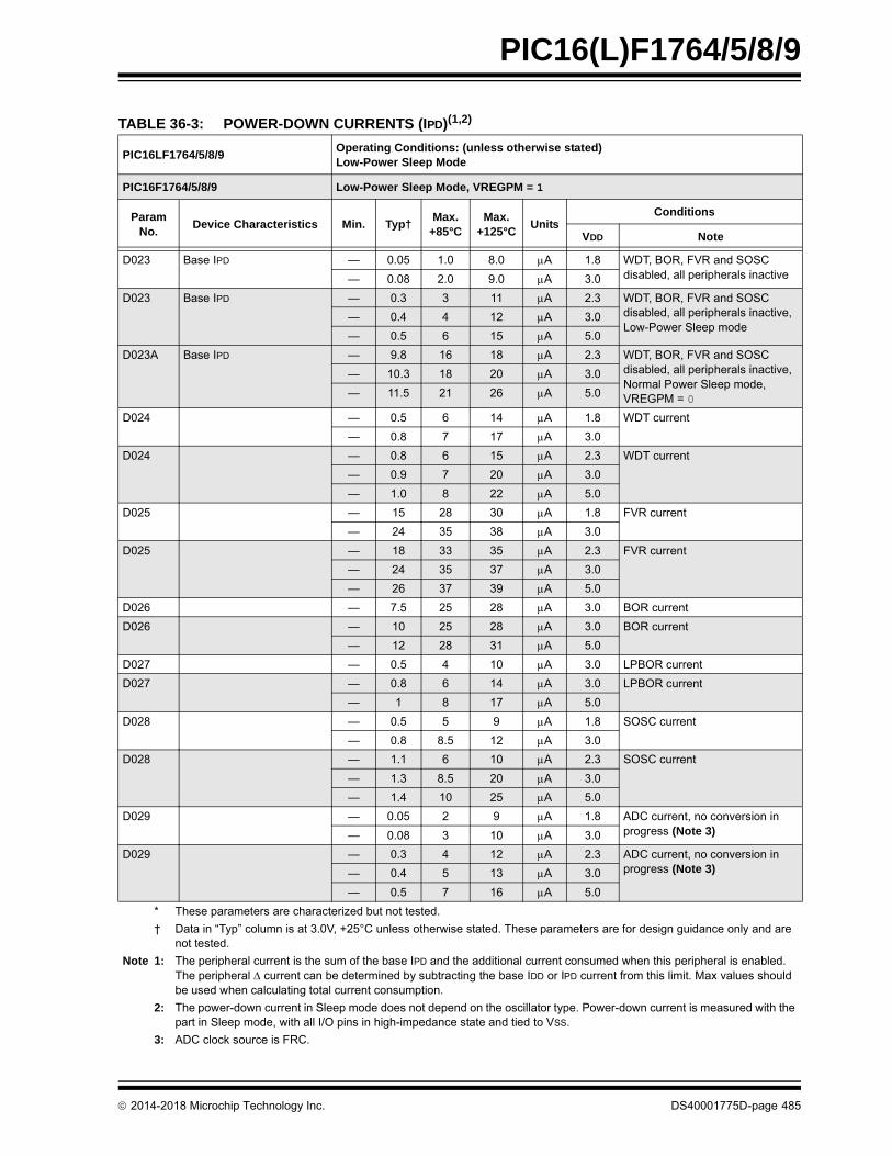
2014-2018 Microchip Technology Inc. DS40001775D-page 485
PIC16(L)F1764/5/8/9
TABLE 36-3: POWER-DOWN CURRENTS (IPD)(1,2)
PIC16LF1764/5/8/9Operating Conditions: (unless otherwise stated)Low-Power Sleep Mode
PIC16F1764/5/8/9 Low-Power Sleep Mode, VREGPM = 1
ParamNo.
Device Characteristics Min. Typ†Max.
+85°CMax.
+125°CUnits
Conditions
VDD Note
D023 Base IPD — 0.05 1.0 8.0 A 1.8 WDT, BOR, FVR and SOSCdisabled, all peripherals inactive— 0.08 2.0 9.0 A 3.0
D023 Base IPD — 0.3 3 11 A 2.3 WDT, BOR, FVR and SOSCdisabled, all peripherals inactive,Low-Power Sleep mode
— 0.4 4 12 A 3.0
— 0.5 6 15 A 5.0
D023A Base IPD — 9.8 16 18 A 2.3 WDT, BOR, FVR and SOSC disabled, all peripherals inactive,Normal Power Sleep mode,VREGPM = 0
— 10.3 18 20 A 3.0
— 11.5 21 26 A 5.0
D024 — 0.5 6 14 A 1.8 WDT current
— 0.8 7 17 A 3.0
D024 — 0.8 6 15 A 2.3 WDT current
— 0.9 7 20 A 3.0
— 1.0 8 22 A 5.0
D025 — 15 28 30 A 1.8 FVR current
— 24 35 38 A 3.0
D025 — 18 33 35 A 2.3 FVR current
— 24 35 37 A 3.0
— 26 37 39 A 5.0
D026 — 7.5 25 28 A 3.0 BOR current
D026 — 10 25 28 A 3.0 BOR current
— 12 28 31 A 5.0
D027 — 0.5 4 10 A 3.0 LPBOR current
D027 — 0.8 6 14 A 3.0 LPBOR current
— 1 8 17 A 5.0
D028 — 0.5 5 9 A 1.8 SOSC current
— 0.8 8.5 12 A 3.0
D028 — 1.1 6 10 A 2.3 SOSC current
— 1.3 8.5 20 A 3.0
— 1.4 10 25 A 5.0
D029 — 0.05 2 9 A 1.8 ADC current, no conversion in progress (Note 3)— 0.08 3 10 A 3.0
D029 — 0.3 4 12 A 2.3 ADC current, no conversion in progress (Note 3)— 0.4 5 13 A 3.0
— 0.5 7 16 A 5.0
* These parameters are characterized but not tested.
† Data in “Typ” column is at 3.0V, +25°C unless otherwise stated. These parameters are for design guidance only and are not tested.
Note 1: The peripheral current is the sum of the base IPD and the additional current consumed when this peripheral is enabled. The peripheral current can be determined by subtracting the base IDD or IPD current from this limit. Max values should be used when calculating total current consumption.
2: The power-down current in Sleep mode does not depend on the oscillator type. Power-down current is measured with the part in Sleep mode, with all I/O pins in high-impedance state and tied to VSS.
3: ADC clock source is FRC.

2014-2018 Microchip Technology Inc. DS40001775D-page 486
PIC16(L)F1764/5/8/9
D030 — 250 — — A 1.8 ADC current, conversion in progress (Note 3)— 250 — — A 3.0
D030 — 280 — — A 2.3 ADC current, conversion in progress (Note 3)— 280 — — A 3.0
— 380 — — A 5.0
D031 — 250 650 — A 3.0 Op Amp (high power)
D031 — 250 650 — A 3.0 Op Amp (high power)
— 350 850 — A 5.0
D032 — 250 600 — A 1.8 Comparator
— 300 650 — A 3.0
D032 — 280 600 — A 2.3 Comparator,VREGPM = 0— 300 650 — A 3.0
— 310 650 — A 5.0
TABLE 36-3: POWER-DOWN CURRENTS (IPD)(1,2) (CONTINUED)
PIC16LF1764/5/8/9Operating Conditions: (unless otherwise stated)Low-Power Sleep Mode
PIC16F1764/5/8/9 Low-Power Sleep Mode, VREGPM = 1
ParamNo.
Device Characteristics Min. Typ†Max.
+85°CMax.
+125°CUnits
Conditions
VDD Note
* These parameters are characterized but not tested.
† Data in “Typ” column is at 3.0V, +25°C unless otherwise stated. These parameters are for design guidance only and are not tested.
Note 1: The peripheral current is the sum of the base IPD and the additional current consumed when this peripheral is enabled. The peripheral current can be determined by subtracting the base IDD or IPD current from this limit. Max values should be used when calculating total current consumption.
2: The power-down current in Sleep mode does not depend on the oscillator type. Power-down current is measured with the part in Sleep mode, with all I/O pins in high-impedance state and tied to VSS.
3: ADC clock source is FRC.

2014-2018 Microchip Technology Inc. DS40001775D-page 487
PIC16(L)F1764/5/8/9
TABLE 36-4: I/O PORTS
Standard Operating Conditions (unless otherwise stated)
ParamNo.
Sym. Characteristic Min. Typ† Max. Units Conditions
VIL Input Low Voltage
I/O Ports:
D034 with TTL Buffer — — 0.8 V 4.5V VDD 5.5V
D034A — — 0.15 VDD V 1.8V VDD 4.5V
D035 with Schmitt Trigger Buffer — — 0.2 VDD V 2.0V VDD 5.5V
with I2C Levels — — 0.3 VDD V
with SMBus Levels — — 0.8 V 2.7V VDD 5.5V
D036 MCLR, OSC1 (EXTRC mode) — — 0.2 VDD V (Note 1)
D036A OSC1 (HS mode) — — 0.3 VDD V
VIH Input High Voltage
I/O Ports:
D040 with TTL Buffer 2.0 — — V 4.5V VDD 5.5V
D040A 0.25 VDD + 0.8 — — V 1.8V VDD 4.5V
D041 with Schmitt Trigger Buffer 0.8 VDD — — V 2.0V VDD 5.5V
with I2C Levels 0.7 VDD — — V
with SMBus Levels 2.1 — — V 2.7V VDD 5.5V
D042 MCLR 0.8 VDD — — V
D043A OSC1 (HS mode) 0.7 VDD — — V
D043B OSC1 (EXTRC oscillator) 0.9 VDD — — V VDD 2.0V(Note 1)
IIL Input Leakage Current(2)
D060 I/O Ports — ± 5 ± 125 nA VSS VPIN VDD, Pin at high-impedance, +85°C
— ± 5 ± 1000 nA VSS VPIN VDD, Pin at high-impedance, +125°C
D061 MCLR(3) — ± 50 ± 200 nA VSS VPIN VDD, Pin at high-impedance, +85°C
IPUR Weak Pull-up Current
D070* 25 100 200 A VDD = 3.3V, VPIN = VSS
25 140 300 A VDD = 5.0V, VPIN = VSS
VOL Output Low Voltage(4)
D080 Standard I/O ports — — 0.6 V IOL = 8mA, VDD = 5VIOL = 6mA, VDD = 3.3VIOL = 1.8mA, VDD = 1.8V
D080A High Drive I/O ports ———
—0.60.6
0.6——
VVV
IOH = 10mA, VDD = 2.3V, HIDCx = 1IOH = 32mA, VDD = 3.0V, HIDCx = 1IOH = 51mA, VDD = 5.0V, HIDCx = 1
* These parameters are characterized but not tested.
† Data in “Typ” column is at 3.0V, +25°C unless otherwise stated. These parameters are for design guidance only and are not tested.
Note 1: In EXTRC oscillator configuration, the OSC1/CLKIN pin is a Schmitt Trigger input. It is not recommended to use an external clock in EXTRC mode.
2: Negative current is defined as current sourced by the pin.
3: The leakage current on the MCLR pin is strongly dependent on the applied voltage level. The specified levels represent normal operating conditions. Higher leakage current may be measured at different input voltages.
4: Including OSC2 in CLKOUT mode.

2014-2018 Microchip Technology Inc. DS40001775D-page 488
PIC16(L)F1764/5/8/9
VOH Output High Voltage(4)
D090 Standard I/O Ports VDD – 0.7 — — V IOH = 3.5mA, VDD = 5VIOH = 3mA, VDD = 3.3VIOH = 1mA, VDD = 1.8V
D090A High Drive I/O Ports VDD – 0.7——
—VDD - 0.7VDD - 0.7
———
VVV
IOH = 10mA, VDD = 2.3V, HIDCX = 1IOH = 37mA, VDD = 3.0V, HIDCX = 1IOH = 54mA, VDD = 5.0V, HIDCX = 1
Capacitive Loading Specs on Output Pins
D101* COSC2 OSC2 Pin — — 15 pF In XT, HS and LP modes when external clock is used to drive OSC1
D101A* CIO All I/O Pins — — 50 pF
TABLE 36-4: I/O PORTS (CONTINUED)
Standard Operating Conditions (unless otherwise stated)
ParamNo.
Sym. Characteristic Min. Typ† Max. Units Conditions
* These parameters are characterized but not tested.
† Data in “Typ” column is at 3.0V, +25°C unless otherwise stated. These parameters are for design guidance only and are not tested.
Note 1: In EXTRC oscillator configuration, the OSC1/CLKIN pin is a Schmitt Trigger input. It is not recommended to use an external clock in EXTRC mode.
2: Negative current is defined as current sourced by the pin.
3: The leakage current on the MCLR pin is strongly dependent on the applied voltage level. The specified levels represent normal operating conditions. Higher leakage current may be measured at different input voltages.
4: Including OSC2 in CLKOUT mode.

2014-2018 Microchip Technology Inc. DS40001775D-page 489
PIC16(L)F1764/5/8/9
TABLE 36-5: MEMORY PROGRAMMING SPECIFICATIONS
Standard Operating Conditions (unless otherwise stated)
ParamNo.
Sym. Characteristic Min. Typ† Max. Units Conditions
Program Memory Programming Specifications
D110 VIHH Voltage on MCLR/VPP Pin 8.0 — 9.0 V (Note 2)
D111 IDDP Supply Current during Programming
— — 10 mA
D112 VBE VDD for Bulk Erase 2.7 — VDDMAX V
D113 VPEW VDD for Write or Row Erase VDDMIN — VDDMAX V
D114 IPPPGM Current on MCLR/VPP during Erase/Write
— 1.0 — mA
D115 IDDPGM Current on VDD during Erase/Write
— 5.0 — mA
Program Flash Memory
D121 EP Cell Endurance 10K — — E/W -40C TA +85C(Note 1)
D122 VPRW VDD for Read/Write VDDMIN — VDDMAX V
D123 TIW Self-Timed Write Cycle Time — 2 2.5 ms
D124 TRETD Characteristic Retention — 40 — Year Provided no other specifications are violated
D125 EHEFC High-Endurance Flash Cell 100K — — E/W -0C TA +60°C, Lower byte last 128 addresses
† Data in “Typ” column is at 3.0V, +25°C unless otherwise stated. These parameters are for design guidance only and are not tested.
Note 1: Self-write and block erase.
2: Required only if single-supply programming is disabled.

2014-2018 Microchip Technology Inc. DS40001775D-page 490
PIC16(L)F1764/5/8/9
TABLE 36-6: THERMAL CHARACTERISTICS
Standard Operating Conditions (unless otherwise stated)
ParamNo.
Sym. Characteristic Typ. Units Conditions
TH01 JA Thermal Resistance Junction to Ambient 70.0 C/W 14-pin PDIP package
95.3 C/W 14-pin SOIC package
100.0 C/W 14-pin TSSOP package
51.5 C/W 16-pin QFN 4x4 mm package
62.2 C/W 20-pin PDIP package
87.3 C/W 20-pin SSOP
77.7 C/W 20-pin SOIC package
43.0 C/W 20-pin QFN 4x4 mm package
TH02 JC Thermal Resistance Junction to Case 32.75 C/W 14-pin PDIP package
31.0 C/W 14-pin SOIC package
24.4 C/W 14-pin TSSOP package
5.4 C/W 16-pin QFN 4x4 mm package
27.5 C/W 20-pin PDIP package
31.1 C/W 20-pin SSOP
23.1 C/W 20-pin SOIC package
5.3 C/W 20-pin QFN 4x4 mm package
TH03 TJMAX Maximum Junction Temperature 150 C
TH04 PD Power Dissipation — W PD = PINTERNAL + PI/O
TH05 PINTERNAL Internal Power Dissipation — W PINTERNAL = IDD x VDD(1)
TH06 PI/O I/O Power Dissipation — W PI/O = (IOL * VOL) + (IOH * (VDD – VOH))
TH07 PDER Derated Power — W PDER = PDMAX (TJ – TA)/JA(2)
Note 1: IDD is current to run the chip alone without driving any load on the output pins.
2: TA = Ambient Temperature, TJ = Junction Temperature.

2014-2018 Microchip Technology Inc. DS40001775D-page 491
PIC16(L)F1764/5/8/9
36.4 AC Characteristics
Timing Parameter Symbology has been created with one of the following formats:
FIGURE 36-4: LOAD CONDITIONS
1. TppS2ppS
2. TppS
T
F Frequency T Time
Lowercase letters (pp) and their meanings:
pp
cc CCP1 osc OSC1
ck CLKOUT rd RD
cs CS rw RD or WR
di SDI sc SCK
do SDO ss SS
dt Data in t0 T0CKI
io I/O PORT t1 T1CKI
mc MCLR wr WR
Uppercase letters and their meanings:
S
F Fall P Period
H High R Rise
I Invalid (High-impedance) V Valid
L Low Z High-impedance
Load Condition
Legend: CL=50 pF for all pins
Pin
CL
VSS
Rev. 10-000133A8/1/2013

2014-2018 Microchip Technology Inc. DS40001775D-page 492
PIC16(L)F1764/5/8/9
FIGURE 36-5: CLOCK TIMING
TABLE 36-7: CLOCK OSCILLATOR TIMING REQUIREMENTS
Standard Operating Conditions (unless otherwise stated)
ParamNo.
Sym. Characteristic Min. Typ† Max. Units Conditions
OS01 FOSC External CLKIN Frequency(1) DC — 0.5 MHz External Clock (ECL)
DC — 4 MHz External Clock (ECM)
DC — 20 MHz External Clock (ECH)
Oscillator Frequency(1) — 32.768 — kHz LP Oscillator
0.1 — 4 MHz XT Oscillator
1 — 4 MHz HS Oscillator
1 — 20 MHz HS Oscillator, VDD > 2.7V
DC — 4 MHz EXTRC, VDD > 2.0V
OS02 TOSC External CLKIN Period(1) 27 — s LP Oscillator
250 — ns XT Oscillator
50 — ns HS Oscillator
50 — ns External Clock (EC)
Oscillator Period(1) — 30.5 — s LP Oscillator
250 — 10,000 ns XT Oscillator
50 — 1,000 ns HS Oscillator
250 — — ns EXTRC
OS03 TCY Instruction Cycle Time(1) 125 TCY DC ns TCY = 4/FOSC
OS04* TosH,TosL
External CLKIN High,External CLKIN Low
2 — — s LP Oscillator
100 — — ns XT Oscillator
20 — — ns HS Oscillator
OS05* TosR,TosF
External CLKIN Rise,External CLKIN Fall
0 — ns LP Oscillator
0 — ns XT Oscillator
0 — ns HS Oscillator
* These parameters are characterized but not tested.† Data in “Typ” column is at 3.0V, +25°C unless otherwise stated. These parameters are for design guidance
only and are not tested.Note 1: Instruction cycle period (TCY) equals four times the input oscillator time base period. All specified values are
based on characterization data for that particular oscillator type under standard operating conditions with the device executing code. Exceeding these specified limits may result in an unstable oscillator operation and/or higher than expected current consumption. All devices are tested to operate at “min” values with an external clock applied to the OSC1 pin. When an external clock input is used, the “max” cycle time limit is “DC” (no clock) for all devices.
CLKIN
CLKOUT
Q4 Q1 Q2 Q3 Q4 Q1
OS02
OS03
(CLKOUT Mode)
Note 1: See Table 36-10.
OS11OS12
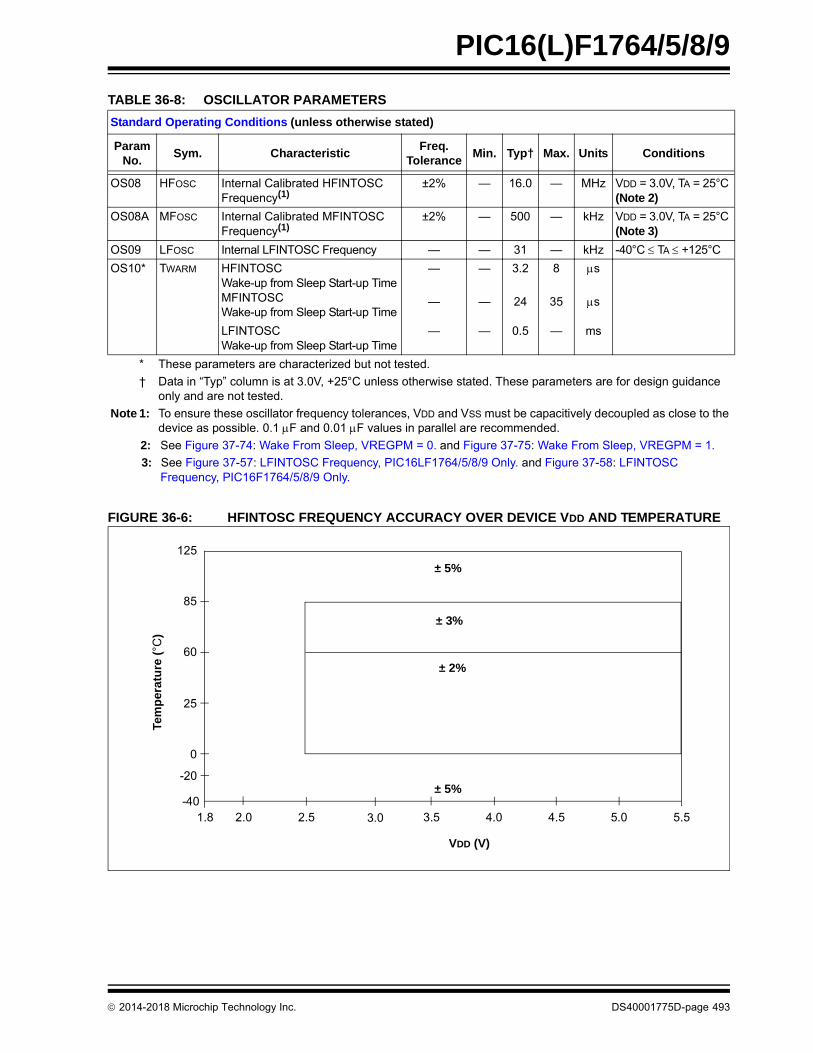
2014-2018 Microchip Technology Inc. DS40001775D-page 493
PIC16(L)F1764/5/8/9
TABLE 36-8: OSCILLATOR PARAMETERS
FIGURE 36-6: HFINTOSC FREQUENCY ACCURACY OVER DEVICE VDD AND TEMPERATURE
Standard Operating Conditions (unless otherwise stated)
Param No.
Sym. CharacteristicFreq.
ToleranceMin. Typ† Max. Units Conditions
OS08 HFOSC Internal Calibrated HFINTOSC Frequency(1)
±2% — 16.0 — MHz VDD = 3.0V, TA = 25°C(Note 2)
OS08A MFOSC Internal Calibrated MFINTOSC Frequency(1)
±2% — 500 — kHz VDD = 3.0V, TA = 25°C(Note 3)
OS09 LFOSC Internal LFINTOSC Frequency — — 31 — kHz -40°C TA +125°C
OS10* TWARM HFINTOSCWake-up from Sleep Start-up TimeMFINTOSCWake-up from Sleep Start-up Time
— — 3.2 8 s
— — 24 35 s
LFINTOSC Wake-up from Sleep Start-up Time
— — 0.5 — ms
* These parameters are characterized but not tested.
† Data in “Typ” column is at 3.0V, +25°C unless otherwise stated. These parameters are for design guidance only and are not tested.
Note 1: To ensure these oscillator frequency tolerances, VDD and VSS must be capacitively decoupled as close to the device as possible. 0.1 F and 0.01 F values in parallel are recommended.
2: See Figure 37-74: Wake From Sleep, VREGPM = 0. and Figure 37-75: Wake From Sleep, VREGPM = 1.
3: See Figure 37-57: LFINTOSC Frequency, PIC16LF1764/5/8/9 Only. and Figure 37-58: LFINTOSC Frequency, PIC16F1764/5/8/9 Only.
125
25
2.0
0
60
85
VDD (V)
4.0 5.04.5
Tem
per
atu
re (
°C)
2.5 3.0 3.5 5.51.8-40
-20
± 5%
± 2%
± 5%
± 3%

2014-2018 Microchip Technology Inc. DS40001775D-page 494
PIC16(L)F1764/5/8/9
TABLE 36-9: PLL CLOCK TIMING SPECIFICATIONS
Standard Operating Conditions (unless otherwise stated)
Param No.
Sym. Characteristic Min. Typ† Max. Units Conditions
F10 FOSC Oscillator Frequency Range 4 — 8 MHz
F11 FSYS On-Chip VCO System Frequency 16 — 32 MHz
F12 TRC PLL Start-up Time (Lock Time) — — 2 ms
F13* CLK CLKOUT Stability (Jitter) -0.25% — +0.25% %
* These parameters are characterized but not tested.
† Data in “Typ” column is at 5V, +25C unless otherwise stated. These parameters are for design guidance only and are not tested.
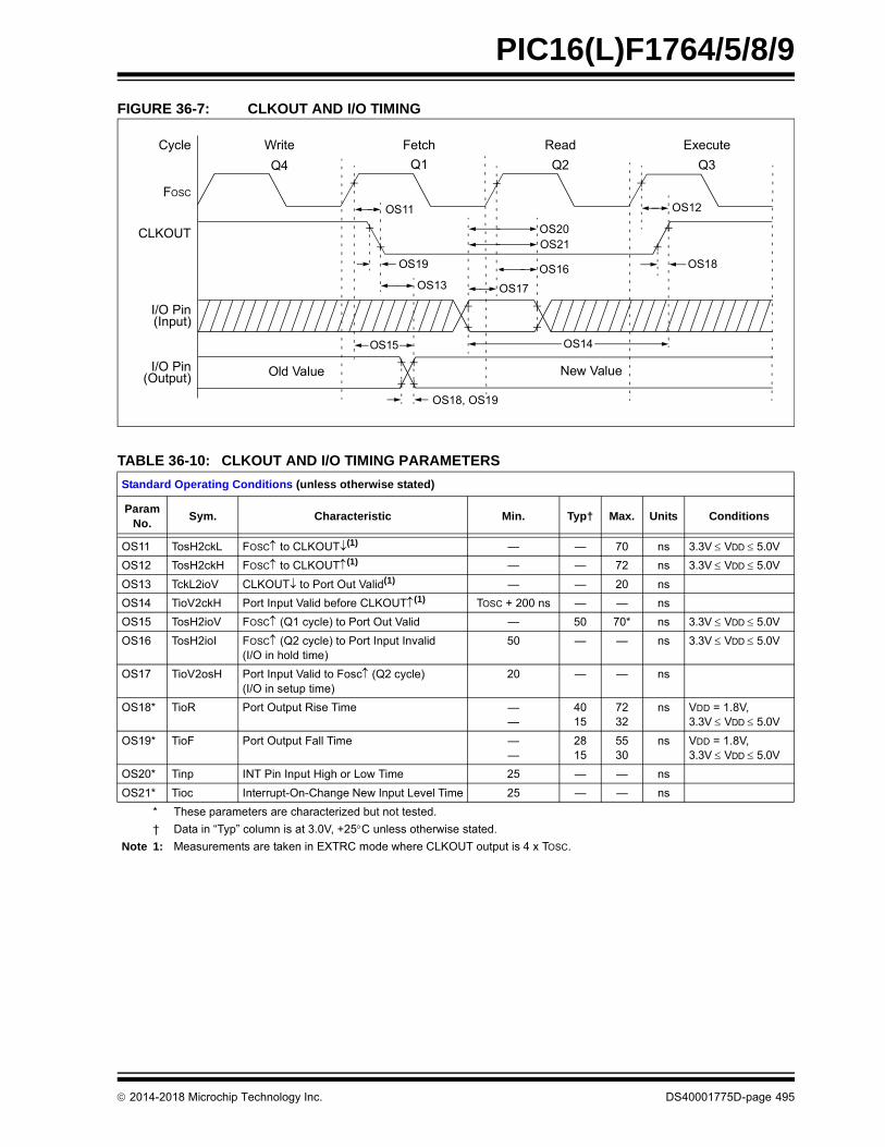
2014-2018 Microchip Technology Inc. DS40001775D-page 495
PIC16(L)F1764/5/8/9
FIGURE 36-7: CLKOUT AND I/O TIMING
TABLE 36-10: CLKOUT AND I/O TIMING PARAMETERS
Standard Operating Conditions (unless otherwise stated)
Param No.
Sym. Characteristic Min. Typ† Max. Units Conditions
OS11 TosH2ckL FOSC to CLKOUT(1) — — 70 ns 3.3V VDD 5.0V
OS12 TosH2ckH FOSC to CLKOUT(1) — — 72 ns 3.3V VDD 5.0V
OS13 TckL2ioV CLKOUT to Port Out Valid(1) — — 20 ns
OS14 TioV2ckH Port Input Valid before CLKOUT(1) TOSC + 200 ns — — ns
OS15 TosH2ioV FOSC (Q1 cycle) to Port Out Valid — 50 70* ns 3.3V VDD 5.0V
OS16 TosH2ioI FOSC (Q2 cycle) to Port Input Invalid (I/O in hold time)
50 — — ns 3.3V VDD 5.0V
OS17 TioV2osH Port Input Valid to Fosc(Q2 cycle)(I/O in setup time)
20 — — ns
OS18* TioR Port Output Rise Time ——
4015
7232
ns VDD = 1.8V,3.3V VDD 5.0V
OS19* TioF Port Output Fall Time ——
2815
5530
ns VDD = 1.8V,3.3V VDD 5.0V
OS20* Tinp INT Pin Input High or Low Time 25 — — ns
OS21* Tioc Interrupt-On-Change New Input Level Time 25 — — ns
* These parameters are characterized but not tested.
† Data in “Typ” column is at 3.0V, +25C unless otherwise stated.
Note 1: Measurements are taken in EXTRC mode where CLKOUT output is 4 x TOSC.
FOSC
CLKOUT
I/O Pin(Input)
I/O Pin(Output)
Q4 Q1 Q2 Q3
OS11
OS19
OS13
OS15
OS18, OS19
OS20OS21
OS17
OS16
OS14
OS12
OS18
Old Value New Value
Write Fetch Read ExecuteCycle

2014-2018 Microchip Technology Inc. DS40001775D-page 496
PIC16(L)F1764/5/8/9
FIGURE 36-8: RESET, WATCHDOG TIMER, OSCILLATOR START-UP TIMER AND POWER-UP TIMER TIMING
VDD
MCLR
InternalPOR
PWRTTime-out
OSCStart-up Time
Internal Reset(1)
Watchdog Timer
33
32
30
3134
I/O Pins
34
Note 1: Asserted low.
Reset(1)

2014-2018 Microchip Technology Inc. DS40001775D-page 497
PIC16(L)F1764/5/8/9
TABLE 36-11: RESET, WATCHDOG TIMER, OSCILLATOR START-UP TIMER, POWER-UP TIMER AND BROWN-OUT RESET PARAMETERS
Standard Operating Conditions (unless otherwise stated)
Param No.
Sym. Characteristic Min. Typ† Max. Units Conditions
30 TMCL MCLR Pulse Width (low) 2 — — s
31 TWDTLP Low-Power Watchdog Timer Time-out Period
10 16 27 ms VDD = 3.3V-5V,1:512 prescaler used
32 TOST Oscillator Start-up Timer Period(1) — 1024 — Tosc
33* TPWRT Power-up Timer Period, PWRTE = 0 40 65 140 ms
34* TIOZ I/O High-Impedance from MCLR Low or Watchdog Timer Reset
— — 2.0 s
35 VBOR Brown-out Reset Voltage(2) 2.552.301.80
2.702.451.90
2.852.602.10
VVV
BORV = 0BORV = 1 (PIC16F1764/5/8/9)BORV = 1 (PIC16LF1764/5/8/9)
35A VLPBOR Low-Power Brown-out 1.8 2.1 2.5 V LPBOR = 1
36* VHYST Brown-out Reset Hysteresis 0 25 75 mV -40°C TA +85°C
37* TBORDC Brown-out Reset DC Response Time 1 3 35 s VDD VBOR
* These parameters are characterized but not tested.
† Data in “Typ” column is at 3.0V, +25°C unless otherwise stated. These parameters are for design guidance only and are not tested.
Note 1: By design, the Oscillator Start-up Timer (OST) counts the first 1024 cycles, independent of frequency.
2: To ensure these voltage tolerances, VDD and VSS must be capacitively decoupled as close to the device as possible. 0.1 F and 0.01 F values in parallel are recommended.

2014-2018 Microchip Technology Inc. DS40001775D-page 498
PIC16(L)F1764/5/8/9
FIGURE 36-9: TIMER0 AND TIMER1 EXTERNAL CLOCK TIMINGS
FIGURE 36-10: BROWN-OUT RESET TIMING AND CHARACTERISTICS
T0CKI
T1CKI
40 41
42
45 46
47 49
TMR0 orTMR1
VBOR
VDD
(Device in Brown-out Reset) (Device not in Brown-out Reset)
33(1)
Reset(due to BOR)
VBOR and VHYST
37
Note 1: The delay (TPWRT) releasing Reset only occurs when the Power-up Timer is enabled (PWRTE = 0).

2014-2018 Microchip Technology Inc. DS40001775D-page 499
PIC16(L)F1764/5/8/9
TABLE 36-12: TIMER0 AND TIMER1 EXTERNAL CLOCK REQUIREMENTS
Standard Operating Conditions (unless otherwise stated)Operating Temperature -40°C TA +125°C
Param No.
Sym. Characteristic Min. Typ† Max. Units Conditions
40* TT0H T0CKI High Pulse Width No Prescaler 0.5 TCY + 20 — — ns
With Prescaler 10 — — ns
41* TT0L T0CKI Low Pulse Width No Prescaler 0.5 TCY + 20 — — ns
With Prescaler 10 — — ns
42* TT0P T0CKI Period Greater of:20 or TCY + 40
N
— — ns N = prescale value
45* TT1H T1CKI High Time
Synchronous, No Prescaler 0.5 TCY + 20 — — ns
Synchronous, with Prescaler 15 — — ns
Asynchronous 30 — — ns
46* TT1L T1CKI Low Time
Synchronous, No Prescaler 0.5 TCY + 20 — — ns
Synchronous, with Prescaler 15 — — ns
Asynchronous 30 — — ns
47* TT1P T1CKI Input Period
Synchronous Greater of:30 or TCY + 40
N
— — ns N = prescale value
Asynchronous 60 — — ns
48 FT1 Secondary Oscillator Input Frequency Range (oscillator enabled by setting bit, T1OSCEN)
32.4 32.768 33.1 kHz
49* TCKEZTMR1 Delay from External Clock Edge to Timer Increment
2 TOSC — 7 TOSC — Timers in Sync mode
* These parameters are characterized but not tested.
† Data in “Typ” column is at 3.0V, +25°C unless otherwise stated. These parameters are for design guidance only and are not tested.

2014-2018 Microchip Technology Inc. DS40001775D-page 500
PIC16(L)F1764/5/8/9
FIGURE 36-11: CAPTURE/COMPARE/PWM TIMINGS (CCP)
TABLE 36-13: CAPTURE/COMPARE/PWM REQUIREMENTS (CCP)
Standard Operating Conditions (unless otherwise stated)
Param No.
Sym. Characteristic Min. Typ† Max. Units Conditions
CC01* TccL CCPx Input Low Time No Prescaler 0.5TCY + 20 — — ns
With Prescaler 20 — — ns
CC02* TccH CCPx Input High Time No Prescaler 0.5TCY + 20 — — ns
With Prescaler 20 — — ns
CC03* TccP CCPx Input Period 3 TCY + 40N
— — ns N = prescale value
* These parameters are characterized but not tested.† Data in “Typ” column is at 3.0V, +25°C unless otherwise stated. These parameters are for design guidance only and are
not tested.
Note: Refer to Figure 36-4 for load conditions.
(Capture mode)
CC01 CC02
CC03
CCPx

2014-2018 Microchip Technology Inc. DS40001775D-page 501
PIC16(L)F1764/5/8/9
FIGURE 36-12: CLC PROPAGATION TIMING
TABLE 36-14: CONFIGURATION LOGIC CELL (CLC) CHARACTERISTICS
Standard Operating Conditions (unless otherwise stated)Operating temperature -40°C TA +125°C
Param. No.
Sym. Characteristic Min. Typ† Max. Units Conditions
CLC01* TCLCIN CLC Input Time — 7 OS17 ns (Note 1)
CLC02* TCLC CLC Module Input to Output Progagation Time ——
2412
——
nsns
VDD = 1.8VVDD > 3.6V
CLC03* TCLCOUT CLC Output Time Rise Time — OS18 — — (Note 1)
Fall Time — OS19 — — (Note 1)
CLC04* FCLCMAX CLC Maximum Switching Frequency — 45 — MHz
* These parameters are characterized but not tested.† Data in “Typ” column is at 3.0V, +25°C unless otherwise stated. These parameters are for design guidance only and are
not tested.Note 1: See Table 36-10 for OS17, OS18 and OS19 rise and fall times.
LCx_in[n](1)
CLCOutput time
CLCInput time LCx_out(1)
CLCxCLCxINnCLC
Module
CLC01 CLC02 CLC03
LCx_in[n](1)CLC
Output timeCLC
Input time LCx_out(1)CLCxCLCxINn
CLCModule
Note 1: See Figure 28-1 to identify specific CLC signals.

2014-2018 Microchip Technology Inc. DS40001775D-page 502
PIC16(L)F1764/5/8/9
TABLE 36-15: ANALOG-TO-DIGITAL CONVERTER (ADC) CHARACTERISTICS(1,2,3,4)
TABLE 36-16: ADC CONVERSION REQUIREMENTS
Operating Conditions (unless otherwise stated)VDD = 3.0V, TA = +25°C, Single-Ended, 2 s TAD, VREF+ = 3V, VREF- = VSS
Param No.
Sym. Characteristic Min. Typ† Max. Units Conditions
AD01 NR Resolution — — 10 bit
AD02 EIL Integral Error — — ±1.7 LSb VREF = 3.0V
AD03 EDL Differential Error — — ±1 LSb No missing codes, VREF = 3.0V
AD04 EOFF Offset Error — — ±2.5 LSb VREF = 3.0V
AD05 EGN Gain Error — — ±2.0 LSb VREF = 3.0V
AD06 VREF Reference Voltage 1.8 — VDD V VREF = (VREF+ – VREF-)
AD07 VAIN Full-Scale Range VSS — VREF V
AD08 ZAIN Recommended Impedance of Analog Voltage Source
— — 10 k Can go higher if external 0.01 F capacitor is present on input pin
* These parameters are characterized but not tested.
† Data in “Typ” column is at 3.0V, +25°C unless otherwise stated. These parameters are for design guidance only and are not tested.
Note 1: Total Absolute Error includes integral, differential, offset and gain errors.
2: The ADC conversion result never decreases with an increase in the input voltage and has no missing codes.
3: ADC VREF is from external VREF+ pin, VDD pin or FVR, whichever is selected as reference input.
4: See Section 37.0 “DC and AC Characteristics Graphs and Charts” for operating characterization.
Standard Operating Conditions (unless otherwise stated)
ParamNo.
Sym. Characteristic Min. Typ† Max. Units Conditions
AD130* TAD ADC Clock Period (TADC) 1.0 — 9.0 s FOSC-based
ADC Internal FRC Oscillator Period (TFRC)
1.0 2 6.0 s ADCS<1:0> = 11 (ADC FRC mode)
AD131 TCNV Conversion Time (not including Acquisition Time)(1)
— 11 — TAD Set GO/DONE bit to conversioncomplete
AD132* TACQ Acquisition Time — 5.0 — s
AD133* THCD Holding Capacitor Disconnect Time — 1/2 TAD — ADCS<2:0> x11 (FOSC-based)
— 1/2 TAD + 1 TCY — ADCS<2:0> = x11 (FRC-based)
* These parameters are characterized but not tested.
† Data in “Typ” column is at 3.0V, +25°C unless otherwise stated. These parameters are for design guidance only and are not tested.
Note 1: The ADRES register may be read on the following TCY cycle.
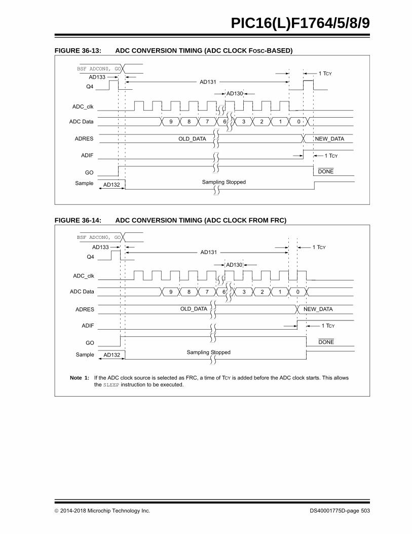
2014-2018 Microchip Technology Inc. DS40001775D-page 503
PIC16(L)F1764/5/8/9
FIGURE 36-13: ADC CONVERSION TIMING (ADC CLOCK FOSC-BASED)
FIGURE 36-14: ADC CONVERSION TIMING (ADC CLOCK FROM FRC)
AD131
AD130
BSF ADCON0, GO
Q4
ADC_clk
ADC Data
ADRES
ADIF
GO
Sample
OLD_DATA
Sampling Stopped
DONE
NEW_DATA
9 8 7 3 2 1 0
1 TCY
6
AD133
1 TCY
AD132
AD132
AD131
AD130
BSF ADCON0, GO
Q4
ADC_clk
ADC Data
ADRES
ADIF
GO
Sample
OLD_DATA
Sampling Stopped
DONE
9 7 3 2 1
Note 1: If the ADC clock source is selected as FRC, a time of TCY is added before the ADC clock starts. This allows the SLEEP instruction to be executed.
AD133
68
1 TCY
1 TCY
0
NEW_DATA

2014-2018 Microchip Technology Inc. DS40001775D-page 504
PIC16(L)F1764/5/8/9
TABLE 36-17: OPERATIONAL AMPLIFIER (OPA)
TABLE 36-18: PROGRAMMABLE RAMP GENERATOR (PRG) SPECIFICATIONS
TABLE 36-19: COMPARATOR SPECIFICATIONS
Operating Conditions (unless otherwise stated)VDD = 3.0V, TA = +25°C, OPAxSP = 1 (High GBWP mode)
ParamNo.
Symbol Parameters Min. Typ. Max. Units Conditions
OPA01* GBWP Gain Bandwidth Product — 3 — MHz
OPA02* TON Turn-on Time — 10 — s
OPA03* PM Phase Margin — 40 — degrees
OPA04* SR Slew Rate — 3 — V/s
OPA05 OFF Offset — ±3 ±9 mV
OPA06 CMRR Common-Mode Rejection Ratio 52 70 — dB
OPA07* AOL Open-Loop Gain — 90 — dB
OPA08 VICM Input Common-Mode Voltage 0 — VDD V VDD > 2.5V
OPA09* PSRR Power Supply Rejection Ratio — 80 — dB
OPA10* HZ High-Impedance On/Off Time — 50 — ns
OPA11* ISC Short Circuit Current — 50 — mA
* These parameters are characterized but not tested.
Operating Conditions (unless otherwise stated)VDD = 3.0V, TA = +25°C (unless otherwise stated)
ParamNo.
Sym. Characteristics Min. Typ. Max. Units Comments
PRG01 RRR Rising Ramp Rate — 1 — V/s PRGxCON2 = 10h
PRG02 FRR Falling Ramp Rate — 1 — V/s PRGxCON2 = 10h
* These parameters are characterized but not tested.
Operating Conditions (unless otherwise stated)VDD = 3.0V, TA = +25°CSee Section 37.0 “DC and AC Characteristics Graphs and Charts” for operating characterization.
ParamNo.
Sym. Characteristics Min. Typ. Max. Units Comments
CM01 VIOFF Input Offset Voltage — ±2.5 ±5 mV VICM = VDD/2
CM02 VICM Input Common-Mode Voltage 0 — VDD V
CM03 CMRR Common-Mode Rejection Ratio 35 50 — dB
CM04A TRESP(1) Response Time Rising Edge — 60 125 ns Normal Power mode
CM04B Response Time Falling Edge — 60 110 ns Normal Power mode
CM04C Response Time Rising Edge — 85 — ns Low-Power mode
CM04D Response Time Falling Edge — 85 — ns Low-Power mode
CM05* TMC2OV Comparator Mode Change to Output Valid*
— — 10 s
CM06 CHYSTER Comparator Hysteresis 20 45 75 mV CxHYS = 1
* These parameters are characterized but not tested.
Note 1: Response time measured with one comparator input at VDD/2, while the other input transitions from VSS to VDD.
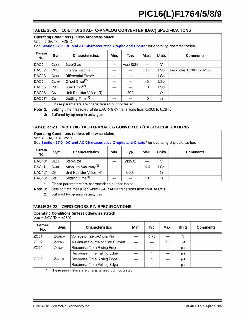
2014-2018 Microchip Technology Inc. DS40001775D-page 505
PIC16(L)F1764/5/8/9
TABLE 36-20: 10-BIT DIGITAL-TO-ANALOG CONVERTER (DAC) SPECIFICATIONS
TABLE 36-21: 5-BIT DIGITAL-TO-ANALOG CONVERTER (DAC) SPECIFICATIONS
TABLE 36-22: ZERO-CROSS PIN SPECIFICATIONS
Operating Conditions (unless otherwise stated)VDD = 3.0V, TA = +25°CSee Section 37.0 “DC and AC Characteristics Graphs and Charts” for operating characterization.
ParamNo.
Sym. Characteristics Min. Typ. Max. Units Comments
DAC01* CLSB Step-Size — VDD/1024 — V
DAC02 CINL Integral Error(2) — — 1.5 LSb For codes: 0x004 to 0x3FB
DAC03 CDNL Differential Error(2) — — 1 LSb
DAC04 COFF Offset Error(2) — — 3 LSb
DAC05 CGN Gain Error(2) — — 3 LSb
DAC06* CR Unit Resistor Value (R) — 300 —
DAC07* CST Settling Time(1) — — 10 s
* These parameters are characterized but not tested.
Note 1: Settling time measured while DACR<9:0> transitions from 0x000 to 0x3FF.
2: Buffered by op amp in unity gain.
Operating Conditions (unless otherwise stated)VDD = 3.0V, TA = +25°CSee Section 37.0 “DC and AC Characteristics Graphs and Charts” for operating characterization.
ParamNo.
Sym. Characteristics Min. Typ. Max. Units Comments
DAC10* CLSB Step-Size — VDD/32 — V
DAC11 CACC Absolute Accuracy(2) — — 0.5 LSb
DAC12* CR Unit Resistor Value (R) — 6000 —
DAC13* CST Settling Time(1) — — 10 s
* These parameters are characterized but not tested.
Note 1: Settling time measured while DACR<4:0> transitions from 0x00 to 0x1F.
2: Buffered by op amp in unity gain.
Operating Conditions (unless otherwise stated)VDD = 3.0V, TA = +25°C
Param.No.
Sym. Characteristics Min. Typ. Max. Units Comments
ZC01 ZCPINV Voltage on Zero-Cross Pin — 0.75 — V
ZC02 ZCDRV Maximum Source or Sink Current — — 600 A
ZC04 ZCISW Response Time Rising Edge — 1 — s
Response Time Falling Edge — 1 — s
ZC05 ZCOUT Response Time Rising Edge — 1 — s
Response Time Falling Edge — 1 — s
* These parameters are characterized but not tested.

2014-2018 Microchip Technology Inc. DS40001775D-page 506
PIC16(L)F1764/5/8/9
FIGURE 36-15: EUSART SYNCHRONOUS TRANSMISSION (MASTER/SLAVE) TIMING
TABLE 36-23: EUSART SYNCHRONOUS TRANSMISSION REQUIREMENTS
FIGURE 36-16: EUSART SYNCHRONOUS RECEIVE (MASTER/SLAVE) TIMING
TABLE 36-24: EUSART SYNCHRONOUS RECEIVE REQUIREMENTS
Standard Operating Conditions (unless otherwise stated)
Param. No.
Symbol Characteristic Min. Max. Units Conditions
US120 TCKH2DTV SYNC XMIT (Master and Slave)Clock High to Data-out Valid
— 80 ns 3.0V VDD 5.5V
— 100 ns 1.8V VDD 5.5V
US121 TCKRF Clock Out Rise Time and Fall Time (Master mode)
— 45 ns 3.0V VDD 5.5V
— 50 ns 1.8V VDD 5.5V
US122 TDTRF Data-out Rise Time and Fall Time — 45 ns 3.0V VDD 5.5V
— 50 ns 1.8V VDD 5.5V
Standard Operating Conditions (unless otherwise stated)
Param. No.
Symbol Characteristic Min. Max. Units Conditions
US125 TDTV2CKL SYNC RCV (Master and Slave)Data-Setup before CK (DT hold time) 10 — ns
US126 TCKL2DTL Data-hold after CK (DT hold time) 15 — ns
Note: Refer to Figure 36-4 for load conditions.
US121 US121
US120 US122
CK
DT
Note: Refer to Figure 36-4 for load conditions.
US125
US126
CK
DT

2014-2018 Microchip Technology Inc. DS40001775D-page 507
PIC16(L)F1764/5/8/9
FIGURE 36-17: SPI MASTER MODE TIMING (CKE = 0, SMP = 0)
FIGURE 36-18: SPI MASTER MODE TIMING (CKE = 1, SMP = 1)
SS
SCK(CKP = 0)
SCK(CKP = 1)
SDO
SDI
SP81
SP71 SP72
SP73SP74
SP75, SP76
SP78SP79SP80
SP79SP78
MSb LSbbit 6 - - - - - -1
LSb Inbit 6 - - - -1MSb In
Note: Refer to Figure 36-4 for load conditions.
SS
SCK(CKP = 0)
SCK(CKP = 1)
SDO
SDI
SP81
SP71 SP72
SP74
SP75, SP76
SP78SP80
SP79SP73
bit 6 - - - - - -1
LSb Inbit 6 - - - -1
LSb
Note: Refer to Figure 36-4 for load conditions.
MSb
MSb In

2014-2018 Microchip Technology Inc. DS40001775D-page 508
PIC16(L)F1764/5/8/9
FIGURE 36-19: SPI SLAVE MODE TIMING (CKE = 0)
FIGURE 36-20: SPI SLAVE MODE TIMING (CKE = 1)
SS
SCK(CKP = 0)
SCK(CKP = 1)
SDO
SDI
SP70
SP71 SP72
SP73
SP74
SP75, SP76 SP77
SP78SP79SP80
SP79SP78
MSb LSbbit 6 - - - - - -1
bit 6 - - - -1 LSb In
SP83
Note: Refer to Figure 36-4 for load conditions.
MSb In
SS
SCK(CKP = 0)
SCK(CKP = 1)
SDO
SDI
SP71 SP72
SP82
SP74
SP75, SP76
MSb bit 6 - - - - - -1 LSb
SP77
bit 6 - - - -1 LSb In
SP80
SP83
Note: Refer to Figure 36-4 for load conditions.
SP70
MSb In

2014-2018 Microchip Technology Inc. DS40001775D-page 509
PIC16(L)F1764/5/8/9
TABLE 36-25: SPI MODE REQUIREMENTS
Standard Operating Conditions (unless otherwise stated)
Param No.
Symbol Characteristic Min. Typ† Max. Units Conditions
SP70* TSSL2SCH, TSSL2SCL
SS to SCK or SCK Input TCY — — ns
SP71* TSCH SCK Input High Time (Slave mode) TCY + 20 — — ns
SP72* TSCL SCK Input Low Time (Slave mode) TCY + 20 — — ns
SP73* TDIV2SCH, TDIV2SCL
Setup Time of SDI Data Input to SCK Edge
100 — — ns
SP74* TSCH2DIL, TSCL2DIL
Hold Time of SDI Data Input to SCK Edge
100 — — ns
SP75* TDOR SDO Data Output Rise Time — 10 25 ns 3.0V VDD 5.5V
— 25 50 ns 1.8V VDD 5.5V
SP76* TDOF SDO Data Output Fall Time — 10 25 ns
SP77* TSSH2DOZ SS to SDO Output High-Impedance
10 — 50 ns
SP78* TSCR SCK Output Rise Time (Master mode)
— 10 25 ns 3.0V VDD 5.5V
— 25 50 ns 1.8V VDD 5.5V
SP79* TSCF SCK Output Fall Time (Master mode)
— 10 25 ns
SP80* TSCH2DOV,TSCL2DOV
SDO Data Output Valid after SCK Edge
— — 50 ns 3.0V VDD 5.5V
— — 145 ns 1.8V VDD 5.5V
SP81* TDOV2SCH,TDOV2SCL
SDO Data Output Setup to SCK Edge
1 TCY — — ns
SP82* TSSL2DOV SDO Data Output Valid after SS Edge
— — 50 ns
SP83* TSCH2SSH,TSCL2SSH
SS after SCK Edge 1.5 TCY + 40 — — ns
* These parameters are characterized but not tested.
† Data in “Typ” column is at 3.0V, +25°C unless otherwise stated. These parameters are for design guidance only and are not tested.

2014-2018 Microchip Technology Inc. DS40001775D-page 510
PIC16(L)F1764/5/8/9
FIGURE 36-21: I2C BUS START/STOP BITS TIMING
TABLE 36-26: I2C BUS START/STOP BITS REQUIREMENTS
FIGURE 36-22: I2C BUS DATA TIMING
Standard Operating Conditions (unless otherwise stated)
ParamNo.
Symbol Characteristic Min. Typ Max. Units Conditions
SP90* TSU:STA Start Condition 100 kHz mode 4700 — — ns Only relevant for Repeated Start conditionSetup Time 400 kHz mode 600 — —
SP91* THD:STA Start Condition 100 kHz mode 4000 — — ns After this period, the first clock pulse is generatedHold Time 400 kHz mode 600 — —
SP92* TSU:STO Stop Condition 100 kHz mode 4700 — — ns
Setup Time 400 kHz mode 600 — —
SP93 THD:STO Stop Condition 100 kHz mode 4000 — — ns
Hold Time 400 kHz mode 600 — —
* These parameters are characterized but not tested.
Note: Refer to Figure 36-4 for load conditions.
SP91
SP92
SP93
SCL
SDA
StartCondition
StopCondition
SP90
Note: Refer to Figure 36-4 for load conditions.
SP90
SP91 SP92
SP100SP101
SP103
SP106SP107
SP109SP109
SP110
SP102
SCL
SDAIn
SDAOut

2014-2018 Microchip Technology Inc. DS40001775D-page 511
PIC16(L)F1764/5/8/9
TABLE 36-27: I2C BUS DATA REQUIREMENTS
Standard Operating Conditions (unless otherwise stated)
Param.No.
Symbol Characteristic Min. Max. Units Conditions
SP100* THIGH Clock High Time 100 kHz mode 4.0 — s Device must operate at a minimum of 1.5 MHz
400 kHz mode 0.6 — s Device must operate at a minimum of 10 MHz
SSP module 1.5 TCY — TCY
SP101* TLOW Clock Low Time 100 kHz mode 4.7 — s Device must operate at a minimum of 1.5 MHz
400 kHz mode 1.3 — s Device must operate at a minimum of 10 MHz
SSP module 1.5 TCY — TCY
SP102* TR SDA and SCL Rise Time
100 kHz mode — 1000 ns
400 kHz mode 20 + 0.1 CB 300 ns CB is specified to be from 10-400 pF
SP103* TF SDA and SCL Fall Time
100 kHz mode — 250 ns
400 kHz mode 20 + 0.1 CB 250 ns CB is specified to be from 10-400 pF
SP106* THD:DAT Data Input Hold Time
100 kHz mode 0 — ns
400 kHz mode 0 0.9 s
SP107* TSU:DAT Data Input Setup Time
100 kHz mode 250 — ns (Note 2)
400 kHz mode 100 — ns
SP109* TAA Output Valid from Clock
100 kHz mode — 3500 ns (Note 1)
400 kHz mode — — ns
SP110* TBUF Bus Free Time 100 kHz mode 4.7 — s Time the bus must be free before a new transmission can start
400 kHz mode 1.3 — s
SP111 CB Bus Capacitive Loading — 400 pF
* These parameters are characterized but not tested.
Note 1: As a transmitter, the device must provide this internal minimum delay time to bridge the undefined region (min. 300 ns) of the falling edge of SCL to avoid unintended generation of Start or Stop conditions.
2: A Fast mode (400 kHz) I2C bus device can be used in a Standard mode (100 kHz) I2C bus system, but the requirement, TSU:DAT 250 ns, must then be met. This will automatically be the case if the device does not stretch the low period of the SCL signal. If such a device does stretch the low period of the SCL signal, it must output the next data bit to the SDA line, TR max. + TSU:DAT = 1000 + 250 = 1250 ns (according to the Standard mode I2C bus specification), before the SCL line is released.

2014-2018 Microchip Technology Inc. DS40001775D-page 512
PIC16(L)F1764/5/8/9
37.0 DC AND AC CHARACTERISTICS GRAPHS AND CHARTS
The graphs and tables provided in this section are for design guidance and are not tested.
In some graphs or tables, the data presented are outside specified operating range (i.e., outside specified VDD
range). This is for information only and devices are ensured to operate properly only within the specified range.
Unless otherwise noted, all graphs apply to both the L and LF devices.
“Typical” represents the mean of the distribution at 25C. “Maximum”, “Max.”, “Minimum” or “Min.”represents (mean + 3) or (mean - 3) respectively, where is a standard deviation, over eachtemperature range.
Note: The graphs and tables provided following this note are a statistical summary based on a limited number ofsamples and are provided for informational purposes only. The performance characteristics listed hereinare not tested or guaranteed. In some graphs or tables, the data presented may be outside the specifiedoperating range (e.g., outside specified power supply range) and therefore, outside the warranted range.

2014-2018 Microchip Technology Inc. DS40001775D-page 513
PIC16(L)F1764/5/8/9
Note: Unless otherwise noted, VIN = 5V, FOSC = 300 kHz, CIN = 0.1 µF, TA = 25°C.
FIGURE 37-1: IDD, LP Oscillator Mode, Fosc = 32 kHz, PIC16LF1764/5/8/9 Only.
FIGURE 37-2: IDD, LP Oscillator Mode, Fosc = 32 kHz, PIC16F1764/5/8/9 Only.
FIGURE 37-3: IDD, XT Oscillator 4 MHz, PIC16LF1764/5/8/9 Only.
FIGURE 37-4: IDD, XT Oscillator, 4 MHz, PIC16F1764/5/8/9 Only.
FIGURE 37-5: IDD, EC Oscillator LP Mode, Fosc = 32 kHz, PIC16LF1764/5/8/9 Only.
FIGURE 37-6: IDD, EC Oscillator LP Mode, Fosc = 32 kHz, PIC16F1764/5/8/9 Only.
Typical
Max.
4
6
8
10
12
14
16
18
1.6 1.8 2.0 2.2 2.4 2.6 2.8 3.0 3.2 3.4 3.6 3.8
IDD
(µA
)
VDD (V)
Max: 85°C + 3Typical: 25°C
Typical
Max.
0
5
10
15
20
25
30
35
40
45
2.0 2.5 3.0 3.5 4.0 4.5 5.0 5.5 6.0
IDD
(µA
)
VDD (V)
Max: 85°C + 3Typical: 25°C
Typical
Max
0
100
200
300
400
500
600
700
1.6 1.8 2.0 2.2 2.4 2.6 2.8 3.0 3.2 3.4 3.6 3.8
IDD
(µA
)
VDD (V)
Max: 85°C + 3Typical: 25°C
Typical
Max
0
100
200
300
400
500
600
700
800
2.0 2.5 3.0 3.5 4.0 4.5 5.0 5.5 6.0
IDD
(µA
)
VDD (V)
Typical: 25°C
Typical
Max.
0
2
4
6
8
10
12
14
1.6 1.8 2.0 2.2 2.4 2.6 2.8 3.0 3.2 3.4 3.6 3.8
IDD
(µA
)
VDD (V)
Max: 85°C + 3Typical: 25°C
Typical
Max.
0
5
10
15
20
25
30
2.0 2.5 3.0 3.5 4.0 4.5 5.0 5.5 6.0
IDD
(µA
)
VDD (V)
Max: 85°C + 3Typical: 25°C

2014-2018 Microchip Technology Inc. DS40001775D-page 514
PIC16(L)F1764/5/8/9
Note: Unless otherwise noted, VIN = 5V, FOSC = 300 kHz, CIN = 0.1 µF, TA = 25°C.
FIGURE 37-7: IDD, EC Oscillator LP Mode, Fosc = 500 kHz, PIC16LF1764/5/8/9 Only.
FIGURE 37-8: IDD, EC Oscillator LP Mode, Fosc = 500 kHz, PIC16F1764/5/8/9 Only.
FIGURE 37-9: IDD Typical, EC Oscillator MP Mode, Fosc = 4 MHz, PIC16LF1764/5/8/9 Only.
FIGURE 37-10: IDD Typical, EC Oscillator MP Mode, Fosc = 4 MHz, PIC16F1764/5/8/9 Only.
FIGURE 37-11: IDD Typical, EC Oscillator HP Mode, PIC16LF1764/5/8/9 Only.
FIGURE 37-12: IDD Maximum, EC Oscillator HP Mode, PIC16LF1764/5/8/9 Only.
Max.
Typical
0
10
20
30
40
50
60
70
1.6 1.8 2.0 2.2 2.4 2.6 2.8 3.0 3.2 3.4 3.6 3.8
IDD
(µA
)
VDD (V)
Max: 85°C + 3Typical: 25°C
Typical
0
10
20
30
40
50
60
70
80
2.0 2.5 3.0 3.5 4.0 4.5 5.0 5.5 6.0
IDD
(µA
)
VDD (V)
Max: 85°C + 3Typical: 25°C
Max
Typical
Max
0
50
100
150
200
250
300
350
400
450
500
1.6 1.8 2.0 2.2 2.4 2.6 2.8 3.0 3.2 3.4 3.6 3.8
IDD
(µA
)
VDD (V)
Max: 85°C + 3Typical: 25°C
Typical
Max
0
100
200
300
400
500
600
700
2.0 2.5 3.0 3.5 4.0 4.5 5.0 5.5 6.0
IDD
(µA
)
VDD (V)
Max: 85°C + 3Typical: 25°C
32 MHz
16 MHz
8 MHz
0.0
0.5
1.0
1.5
2.0
2.5
3.0
3.5
1.6 1.8 2.0 2.2 2.4 2.6 2.8 3.0 3.2 3.4 3.6 3.8
IDD
(mA
)
VDD (V)
Typical: 25°C
32 MHz
16 MHz
8 MHz
0.0
0.5
1.0
1.5
2.0
2.5
3.0
3.5
1.6 1.8 2.0 2.2 2.4 2.6 2.8 3.0 3.2 3.4 3.6 3.8
IDD
(mA
)
VDD (V)
Max: 85°C + 3

2014-2018 Microchip Technology Inc. DS40001775D-page 515
PIC16(L)F1764/5/8/9
Note: Unless otherwise noted, VIN = 5V, FOSC = 300 kHz, CIN = 0.1 µF, TA = 25°C.
FIGURE 37-13: IDD Typical, EC Oscillator HP Mode, PIC16F1764/5/8/9 Only.
FIGURE 37-14: IDD Maximum, EC Oscillator HP Mode, PIC16F1764/5/8/9 Only.
FIGURE 37-15: IDD LFINTOSC Mode, Fosc = 31 kHz, PIC16LF1764/5/8/9 Only.
FIGURE 37-16: IDD LFINTOSC Mode, Fosc = 31 kHz, PIC16F1764/5/8/9 Only.
FIGURE 37-17: IDD, MFINTOSC Mode, Fosc = 500 kHz, PIC16LF1764/5/8/9 Only.
FIGURE 37-18: IDD, MFINTOSC Mode, Fosc = 500 kHz, PIC16F1764/5/8/9 Only.
16MHz
32MHz
8MHz
0.0
0.5
1.0
1.5
2.0
2.5
3.0
2.0 2.5 3.0 3.5 4.0 4.5 5.0 5.5 6.0
IDD
(mA
)
VDD (V)
Typical: 25°C
16MHz
32MHz
8MHz
0.0
0.5
1.0
1.5
2.0
2.5
3.0
3.5
2.0 2.5 3.0 3.5 4.0 4.5 5.0 5.5 6.0
IDD
(mA
)
VDD (V)
Max: 85°C + 3
Typical
Max.
0
1
2
3
4
5
6
7
8
9
1.6 1.8 2.0 2.2 2.4 2.6 2.8 3.0 3.2 3.4 3.6 3.8
IDD
(µA
)
VDD (V)
Max: 85°C + 3Typical: 25°C
Typical
Max.
0
5
10
15
20
25
30
2.0 2.5 3.0 3.5 4.0 4.5 5.0 5.5 6.0
IDD
(µA
)
VDD (V)
Max: 85°C + 3Typical: 25°C
Typical
Max.
100
110
120
130
140
150
160
170
180
190
200
1.6 1.8 2.0 2.2 2.4 2.6 2.8 3.0 3.2 3.4 3.6 3.8
IDD
(µA
)
VDD (V)
Max: 85°C + 3Typical: 25°C
Typical
0
50
100
150
200
250
300
350
2.0 2.5 3.0 3.5 4.0 4.5 5.0 5.5 6.0
IDD
(µA
)
VDD (V)
Max: 85°C + 3Typical: 25°C
Max

2014-2018 Microchip Technology Inc. DS40001775D-page 516
PIC16(L)F1764/5/8/9
Note: Unless otherwise noted, VIN = 5V, FOSC = 300 kHz, CIN = 0.1 µF, TA = 25°C.
FIGURE 37-19: IDD Typical, HFINTOSC Mode, PIC16LF1764/5/8/9 Only.
FIGURE 37-20: IDD Maximum, HFINTOSC Mode, PIC16LF1764/5/8/9 Only.
FIGURE 37-21: IDD Typical, HFINTOSC Mode, PIC16F1764/5/8/9 Only.
FIGURE 37-22: IDD Maximum, HFINTOSC Mode, PIC16F1764/5/8/9 Only.
FIGURE 37-23: IDD Typical, HS Oscillator, 25°C, PIC16LF1764/5/8/9 Only.
FIGURE 37-24: IDD Maximum, HS Oscillator, PIC16LF1764/5/8/9 Only.
1 MHz
2 MHz
4MHz
8 MHz
16MHz
0.0
0.2
0.4
0.6
0.8
1.0
1.2
1.4
1.6
1.8
2.0
1.6 1.8 2.0 2.2 2.4 2.6 2.8 3.0 3.2 3.4 3.6 3.8
IDD
(mA
)
VDD (V)
Typical: 25°C
1 MHz
2 MHz4MHz
8 MHz
16MHz
0.0
0.5
1.0
1.5
2.0
2.5
1.6 1.8 2.0 2.2 2.4 2.6 2.8 3.0 3.2 3.4 3.6 3.8
IDD
(mA
)
VDD (V)
Max: 85°C + 3
1MHz
4MHz
8MHz
16MHz
0.0
0.2
0.4
0.6
0.8
1.0
1.2
1.4
1.6
1.8
2.0 2.5 3.0 3.5 4.0 4.5 5.0 5.5 6.0
IDD
(mA
)
VDD (V)
Typical: 25°C
2MHz
1MHz
2MHz
8MHz
16MHz
0.0
0.2
0.4
0.6
0.8
1.0
1.2
1.4
1.6
1.8
2.0
2.0 2.5 3.0 3.5 4.0 4.5 5.0 5.5 6.0
IDD
(mA
)
VDD (V)
Max: 85°C + 3
4MHz
4 MHz
8 MHz
16 MHz
20 MHz
8MHz w/ 4X PLL
0.0
0.5
1.0
1.5
2.0
2.5
3.0
3.5
1.6 1.8 2.0 2.2 2.4 2.6 2.8 3.0 3.2 3.4 3.6 3.8
IDD
(mA
)
VDD (V)
4 MHz
8 MHz
16 MHz
20 MHz
8MHz w/ 4X PLL
0.0
0.5
1.0
1.5
2.0
2.5
3.0
3.5
4.0
1.6 1.8 2.0 2.2 2.4 2.6 2.8 3.0 3.2 3.4 3.6 3.8
IDD
(mA
)
VDD (V)
Max: 85°C + 3Max: 85°C + 3Max: 85°C + 3Max: 85°C + 3

2014-2018 Microchip Technology Inc. DS40001775D-page 517
PIC16(L)F1764/5/8/9
Note: Unless otherwise noted, VIN = 5V, FOSC = 300 kHz, CIN = 0.1 µF, TA = 25°C.
FIGURE 37-25: IDD Typical, HS Oscillator, 25°C, PIC16F1764/5/8/9 Only.
FIGURE 37-26: IDD Maximum, HS Oscillator, PIC16F1764/5/8/9 Only.
FIGURE 37-27: IPD Base, LP Sleep Mode, PIC16LF1764/5/8/9 Only.
FIGURE 37-28: IPD Base, LP Sleep Mode (VREGPM = 1), PIC16F1764/5/8/9 Only.
FIGURE 37-29: IPD, Watchdog Timer (WDT), PIC16LF1764/5/8/9 Only.
FIGURE 37-30: IPD, Watchdog Timer (WDT), PIC16F1764/5/8/9 Only.
4 MHz
8 MHz
16 MHz
20 MHz
8MHz w/ 4X PLL
0.0
0.5
1.0
1.5
2.0
2.5
3.0
3.5
4.0
2.0 2.5 3.0 3.5 4.0 4.5 5.0 5.5 6.0
IDD
(mA
)
VDD (V)
4 MHz
8 MHz
16 MHz
20 MHz
8MHz w/ 4X PLL
0.0
0.5
1.0
1.5
2.0
2.5
3.0
3.5
4.0
4.5
2.0 2.5 3.0 3.5 4.0 4.5 5.0 5.5 6.0
IDD
(mA
)
VDD (V)
Max: 85°C + 3
Max.
Typical
0
50
100
150
200
250
300
350
400
450
1.6 1.8 2.0 2.2 2.4 2.6 2.8 3.0 3.2 3.4 3.6 3.8
IDD
(nA)
VDD (V)
Max: 85°C + 3Typical: 25°C
Max.
Typical
0.0
0.2
0.4
0.6
0.8
1.0
1.2
2.0 2.5 3.0 3.5 4.0 4.5 5.0 5.5 6.0
IPD
(µA)
VDD (V)
Max: 85°C + 3Typical: 25°C
Max.
Typical
0.0
0.5
1.0
1.5
2.0
2.5
3.0
1.6 1.8 2.0 2.2 2.4 2.6 2.8 3.0 3.2 3.4 3.6 3.8
IPD
(µA)
VDD (V)
Max: 85°C + 3Typical: 25°C
Max.
Typical
0.0
0.5
1.0
1.5
2.0
2.5
2.0 2.5 3.0 3.5 4.0 4.5 5.0 5.5 6.0
IPD
(µA)
VDD (V)
Max: 85°C + 3Typical: 25°C

2014-2018 Microchip Technology Inc. DS40001775D-page 518
PIC16(L)F1764/5/8/9
Note: Unless otherwise noted, VIN = 5V, FOSC = 300 kHz, CIN = 0.1 µF, TA = 25°C.
FIGURE 37-31: IPD, Fixed Voltage Reference (FVR), PIC16LF1764/5/8/9 Only.
FIGURE 37-32: IPD, Fixed Voltage Reference (FVR), PIC16F1764/5/8/9 Only.
FIGURE 37-33: IPD, Brown-Out Reset (BOR), BORV = 1, PIC16LF1764/5/8/9 Only.
FIGURE 37-34: IPD, Brown-Out Reset (BOR), BORV = 1, PIC16F1764/5/8/9 Only.
FIGURE 37-35: IPD, LP Brown-Out Reset (LPBOR = 0), PIC16LF1764/5/8/9 Only.
FIGURE 37-36: IPD, LP Brown-Out Reset (LPBOR = 0), PIC16F1764/5/8/9 Only.
Max.
Typical
5
10
15
20
25
30
35
1.6 1.8 2.0 2.2 2.4 2.6 2.8 3.0 3.2 3.4 3.6 3.8
IDD
(nA)
VDD (V)
Max: 85°C + 3Typical: 25°C
Max.
Typical
0
5
10
15
20
25
30
35
2.0 2.5 3.0 3.5 4.0 4.5 5.0 5.5 6.0
IDD
(nA)
VDD (V)
Max: 85°C + 3Typical: 25°C
Max.
Typical
4
5
6
7
8
9
10
11
2.9 3.0 3.1 3.2 3.3 3.4 3.5 3.6 3.7
IDD
(nA)
VDD (V)
Max: 85°C + 3Typical: 25°C
Max.
Typical
4
5
6
7
8
9
10
11
12
13
2.8 3.0 3.2 3.4 3.6 3.8 4.0 4.2 4.4 4.6 4.8 5.0 5.2 5.4 5.6
IDD
(nA)
VDD (V)
Max: 85°C + 3Typical: 25°C
Max.
Typical
0
0.2
0.4
0.6
0.8
1
1.2
1.4
1.6
1.8
2.9 3.0 3.1 3.2 3.3 3.4 3.5 3.6 3.7
IDD
(nA)
VDD (V)
Max: 85°C + 3Typical: 25°C
Max.
Typical
0.0
0.2
0.4
0.6
0.8
1.0
1.2
1.4
1.6
1.8
2.8 3.0 3.2 3.4 3.6 3.8 4.0 4.2 4.4 4.6 4.8 5.0 5.2 5.4 5.6
IDD
(µA)
VDD (V)
Max: 85°C + 3Typical: 25°C
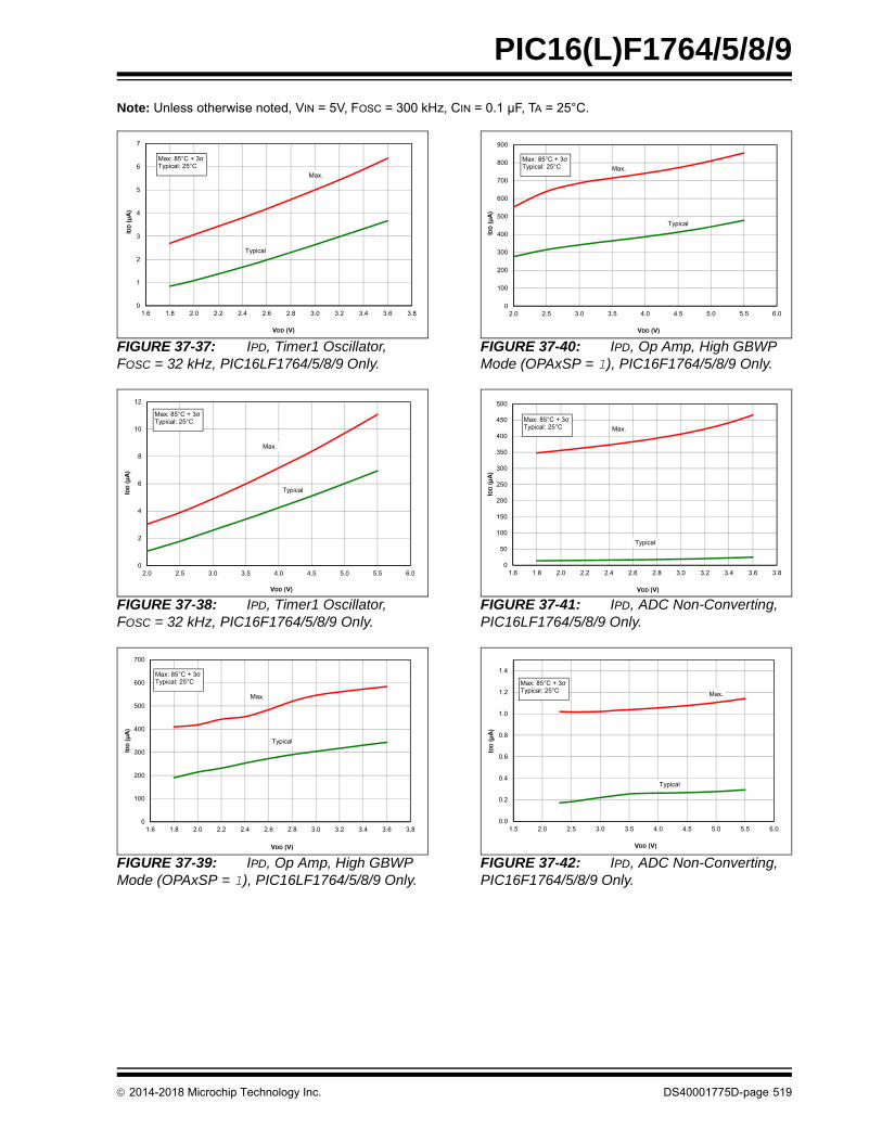
2014-2018 Microchip Technology Inc. DS40001775D-page 519
PIC16(L)F1764/5/8/9
Note: Unless otherwise noted, VIN = 5V, FOSC = 300 kHz, CIN = 0.1 µF, TA = 25°C.
FIGURE 37-37: IPD, Timer1 Oscillator, FOSC = 32 kHz, PIC16LF1764/5/8/9 Only.
FIGURE 37-38: IPD, Timer1 Oscillator, FOSC = 32 kHz, PIC16F1764/5/8/9 Only.
FIGURE 37-39: IPD, Op Amp, High GBWP Mode (OPAxSP = 1), PIC16LF1764/5/8/9 Only.
FIGURE 37-40: IPD, Op Amp, High GBWP Mode (OPAxSP = 1), PIC16F1764/5/8/9 Only.
FIGURE 37-41: IPD, ADC Non-Converting, PIC16LF1764/5/8/9 Only.
FIGURE 37-42: IPD, ADC Non-Converting, PIC16F1764/5/8/9 Only.
Max.
Typical
0
1
2
3
4
5
6
7
1.6 1.8 2.0 2.2 2.4 2.6 2.8 3.0 3.2 3.4 3.6 3.8
IDD
(µA)
VDD (V)
Max: 85°C + 3Typical: 25°C
Max.
Typical
0
2
4
6
8
10
12
2.0 2.5 3.0 3.5 4.0 4.5 5.0 5.5 6.0
IDD
(µA)
VDD (V)
Max: 85°C + 3Typical: 25°C
Max.
Typical
0
100
200
300
400
500
600
700
1.6 1.8 2.0 2.2 2.4 2.6 2.8 3.0 3.2 3.4 3.6 3.8
IDD
(µA)
VDD (V)
Max: 85°C + 3Typical: 25°C
Typical
Max.
0
100
200
300
400
500
600
700
800
900
2.0 2.5 3.0 3.5 4.0 4.5 5.0 5.5 6.0
IDD
(µA)
VDD (V)
Max: 85°C + 3Typical: 25°C
Max.
Typical
0
50
100
150
200
250
300
350
400
450
500
1.6 1.8 2.0 2.2 2.4 2.6 2.8 3.0 3.2 3.4 3.6 3.8
IDD
(µA)
VDD (V)
Max: 85°C + 3Typical: 25°C
Max.
Typical
0.0
0.2
0.4
0.6
0.8
1.0
1.2
1.4
1.5 2.0 2.5 3.0 3.5 4.0 4.5 5.0 5.5 6.0
IDD
(µA)
VDD (V)
Max: 85°C + 3Typical: 25°C

2014-2018 Microchip Technology Inc. DS40001775D-page 520
PIC16(L)F1764/5/8/9
Note: Unless otherwise noted, VIN = 5V, FOSC = 300 kHz, CIN = 0.1 µF, TA = 25°C.
FIGURE 37-43: IPD, Comparator, NP Mode (CxSP = 1), PIC16LF1764/5/8/9 Only.
FIGURE 37-44: IPD, Comparator, NP Mode (CxSP = 1), PIC16F1764/5/8/9 Only.
FIGURE 37-45: Standard IO VOH vs. IOH Over Temperature, VDD = 5.0V, PIC16F1764/5/8/9 Only.
FIGURE 37-46: Standard IO VOL vs. IOL Over Temperature, VDD = 5.0V, PIC16F1764/5/8/9 Only.
FIGURE 37-47: Standard IO VOH vs. IOH Over Temperature, VDD = 3.0V.
FIGURE 37-48: Standard IO VOL vs. IOL Over Temperature, VDD = 3.0V.
Max.
Typical
200
300
400
500
600
700
800
1.6 1.8 2.0 2.2 2.4 2.6 2.8 3.0 3.2 3.4 3.6 3.8
IDD
(µA)
VDD (V)
Max: -40°C + 3Typical: 25°C
Max.
Typical
200
300
400
500
600
700
800
2.0 2.5 3.0 3.5 4.0 4.5 5.0 5.5 6.0
IDD
(µA)
VDD (V)
Max: -40°C + 3Typical: 25°C
-40°C
Typical125°C
0
1
2
3
4
5
6
-30 -25 -20 -15 -10 -5 0
VOH
(V)
IOH (mA)
Graph represents 3Limits
-40°C
Typical
125°C
0
1
2
3
4
5
0 10 20 30 40 50 60 70 80
VOL
(V)
IOL (mA)
Graph represents 3Limits
-40°C
Typical
125°C
0.0
0.5
1.0
1.5
2.0
2.5
3.0
3.5
-14 -12 -10 -8 -6 -4 -2 0
VOH
(V)
IOH (mA)
Graph represents 3Limits
-40°C
125°C
Typical
0.0
0.5
1.0
1.5
2.0
2.5
3.0
0 5 10 15 20 25 30
VOL
(V)
IOL (mA)
Graph represents 3Limits

2014-2018 Microchip Technology Inc. DS40001775D-page 521
PIC16(L)F1764/5/8/9
Note: Unless otherwise noted, VIN = 5V, FOSC = 300 kHz, CIN = 0.1 µF, TA = 25°C.
FIGURE 37-49: Standard IO VOH vs. IOH Over Temperature, VDD = 1.8V, PIC16LF1764/5/8/9 Only.
FIGURE 37-50: Standard IO VOL vs. IOL Over Temperature, VDD = 1.8V, PIC16LF1764/5/8/9 Only.
FIGURE 37-51: 100mA IO VOH vs. IOH Over Temperature, VDD = 5.5V, PIC16F1764/5/8/9 Only.
FIGURE 37-52: 100mA IO VOL vs. IOL Over Temperature, VDD = 5.5V, PIC16F1764/5/8/9 Only.
FIGURE 37-53: 100mA IO VOH vs. IOH Over Temperature, VDD = 3.0V.
FIGURE 37-54: VOL vs. IOL Over Temperature, VDD = 3.0V.
-40°CTypical
125°C
0.0
0.2
0.4
0.6
0.8
1.0
1.2
1.4
1.6
1.8
2.0
-4.0 -3.5 -3.0 -2.5 -2.0 -1.5 -1.0 -0.5 0.0
VOH
(V)
IOH (mA)
Graph represents 3Limits
-40°C
Typical125°C
0.0
0.2
0.4
0.6
0.8
1.0
1.2
1.4
1.6
1.8
0 1 2 3 4 5 6 7 8 9 10
VOL
(V)
IOL (mA)
Graph represents 3 Limits
-40°C
Typical
125°C
0
1
2
3
4
5
6
-200 -150 -100 -50 0
VOH
(V)
IOH (mA)
Graph represents 3Limits
,
-40°C
Typical
125°C
0
1
2
3
4
5
0 50 100 150 200
VOL
(V)
IOL (mA)
Graph represents 3Limits
-40°C
Typical
0.0
0.5
1.0
1.5
2.0
2.5
3.0
3.5
-120 -100 -80 -60 -40 -20 0
VOH
(V)
IOH (mA)
Graph represents 3Limits
125°C
-40°C125°C
Typical
0.0
0.5
1.0
1.5
2.0
2.5
3.0
0 10 20 30 40 50 60 70 80 90 100
VOL
(V)
IOL (mA)
Graph represents 3Limits

2014-2018 Microchip Technology Inc. DS40001775D-page 522
PIC16(L)F1764/5/8/9
Note: Unless otherwise noted, VIN = 5V, FOSC = 300 kHz, CIN = 0.1 µF, TA = 25°C.
FIGURE 37-55: 100mA IO VOH vs. IOH Over Temperature, VDD = 1.8V, PIC16LF1764/5/8/9 Only.
FIGURE 37-56: 100mA IO VOL vs. IOL Over Temperature, VDD = 1.8V, PIC16LF1764/5/8/9 Only.
FIGURE 37-57: LFINTOSC Frequency, PIC16LF1764/5/8/9 Only.
FIGURE 37-58: LFINTOSC Frequency, PIC16F1764/5/8/9 Only.
FIGURE 37-59: WDT Time-Out Period, PIC16F1764/5/8/9 Only.
FIGURE 37-60: WDT Time-Out Period, PIC16LF1764/5/8/9 Only.
-40°C
Typical 125°C
0.0
0.2
0.4
0.6
0.8
1.0
1.2
1.4
1.6
1.8
2.0
-30 -25 -20 -15 -10 -5 0
VOH
(V)
IOH (mA)
Graph represents 3Limits
-40°C
Typical
125°C
0.0
0.2
0.4
0.6
0.8
1.0
1.2
1.4
1.6
1.8
0 5 10 15 20 25 30
VOL
(V)
IOL (mA)
Graph represents 3Limits
Typical
Max.
Min.
20,000
22,000
24,000
26,000
28,000
30,000
32,000
34,000
36,000
38,000
40,000
1.6 1.8 2.0 2.2 2.4 2.6 2.8 3.0 3.2 3.4 3.6 3.8
Freq
uenc
y (H
z)
VDD (V)
Max: Typical + 3 (-40°C to +125°C)Typical; statistical mean @ 25°CMin: Typical - 3 (-40°C to +125°C)
Typical
Max.
Min.
20,000
22,000
24,000
26,000
28,000
30,000
32,000
34,000
36,000
38,000
40,000
2.0 2.5 3.0 3.5 4.0 4.5 5.0 5.5 6.0
Freq
uenc
y (H
z)
VDD (V)
Max: Typical + 3 (-40°C to +125°C)Typical; statistical mean @ 25°CMin: Typical - 3 (-40°C to +125°C)
Typical
Max.
Min.
10
12
14
16
18
20
22
24
2.0 2.5 3.0 3.5 4.0 4.5 5.0 5.5 6.0
Tim
e (m
S)
VDD (V)
Max: Typical + 3 (-40°C to +125°C)Typical; statistical mean @ 25°CMin: Typical - 3 (-40°C to +125°C)
Typical
Max.
Min.
10
12
14
16
18
20
22
24
1.6 1.8 2 2.2 2.4 2.6 2.8 3 3.2 3.4 3.6 3.8
Tim
e (m
S)
VDD (V)
Max: Typical + 3 (-40°C to +125°C)Typical; statistical mean @ 25°CMin: Typical - 3 (-40°C to +125°C)

2014-2018 Microchip Technology Inc. DS40001775D-page 523
PIC16(L)F1764/5/8/9
Note: Unless otherwise noted, VIN = 5V, FOSC = 300 kHz, CIN = 0.1 µF, TA = 25°C.
FIGURE 37-61: Brown-Out Reset Voltage, Low Trip Point (BORV = 1), PIC16LF1764/5/8/9 Only.
FIGURE 37-62: Brown-Out Reset Hysteresis, Low Trip Point (BORV = 1), PIC16LF1764/5/8/9 Only.
FIGURE 37-63: Brown-Out Reset Voltage, Low Trip Point (BORV = 1), PIC16F1764/5/8/9 Only.
FIGURE 37-64: Brown-Out Reset Hysteresis, Low Trip Point (BORV = 1), PIC16F1764/5/8/9 Only.
FIGURE 37-65: Brown-Out Reset Voltage, High Trip Point (BORV = 0).
FIGURE 37-66: Brown-Out Reset Hysteresis, High Trip Point (BORV = 0).
Max.
Min.
Typical
1.80
1.85
1.90
1.95
2.00
-60 -40 -20 0 20 40 60 80 100 120 140
Volta
ge (V
)
Temperature (°C)
Max: Typical + 3Typical: statistical mean Min: Typical - 3
Typical
Max.
Min.
0
10
20
30
40
50
60
70
-60 -40 -20 0 20 40 60 80 100 120 140
Volta
ge (m
V)
Temperature (°C)
Max: Typical + 3Typical: statistical meanMin: Typical - 3
Max.
Min.
Typical
2.30
2.35
2.40
2.45
2.50
2.55
2.60
-60 -40 -20 0 20 40 60 80 100 120 140
Volta
ge (V
)
Temperature (°C)
Max: Typical + 3Typical: statistical meanMin: Typical - 3
Typical
Max.
Min.
0
10
20
30
40
50
60
70
-60 -40 -20 0 20 40 60 80 100 120 140
Volta
ge (m
V)
Temperature (°C)
Max: Typical + 3Typical: statistical mean Min: Typical - 3
Max.
Min.
Typical
2.60
2.65
2.70
2.75
2.80
2.85
-60 -40 -20 0 20 40 60 80 100 120 140
Volta
ge (V
)
Temperature (°C)
Max: Typical + 3Typical: statistical meanMin: Typical - 3
Typical
Max.
Min.
0
10
20
30
40
50
60
70
80
-60 -40 -20 0 20 40 60 80 100 120 140
Volta
ge (m
V)
Temperature (°C)
Max: Typical + 3Typical: statistical mean Min: Typical - 3

2014-2018 Microchip Technology Inc. DS40001775D-page 524
PIC16(L)F1764/5/8/9
Note: Unless otherwise noted, VIN = 5V, FOSC = 300 kHz, CIN = 0.1 µF, TA = 25°C.
FIGURE 37-67: LPBOR Reset Voltage.
FIGURE 37-68: LPBOR Reset Hysteresis.
FIGURE 37-69: PWRT Period, PIC16F1764/5/8/9 Only.
FIGURE 37-70: PWRT Period, PIC16LF1764/5/8/9 Only.
FIGURE 37-71: POR Release Voltage.
FIGURE 37-72: POR Rearm Voltage, NP Mode (VREGPM = 0), PIC16F1764/5/8/9 Only.
Max.
Min.
Typical
1.7
1.8
1.9
2.0
2.1
2.2
2.3
2.4
2.5
2.6
-60 -40 -20 0 20 40 60 80 100 120 140
Volta
ge (V
)
Temperature (°C)
Max: Typical + 3Typical: statistical mean Min: Typical - 3
Typical
Max.
0
5
10
15
20
25
30
35
40
45
50
-60 -40 -20 0 20 40 60 80 100 120 140
Volta
ge (m
V)
Temperature (°C)
Max: Typical + 3Typical: statistical mean
Typical
Max.
Min.
40
50
60
70
80
90
100
2.0 2.5 3.0 3.5 4.0 4.5 5.0 5.5 6.0
Tim
e (m
S)
VDD (V)
Max: Typical + 3 (-40°C to +125°C)Typical; statistical mean @ 25°CMin: Typical - 3 (-40°C to +125°C)
Typical
Max.
Min.
40
50
60
70
80
90
100
110
1.6 1.8 2.0 2.2 2.4 2.6 2.8 3.0 3.2 3.4 3.6 3.8
Tim
e (m
S)
VDD (V)
Max: Typical + 3 (-40°C to +125°C)Typical; statistical mean @ 25°CMin: Typical - 3 (-40°C to +125°C)
Typical
Max.
Min.
1.50
1.52
1.54
1.56
1.58
1.60
1.62
1.64
1.66
1.68
1.70
-60 -40 -20 0 20 40 60 80 100 120 140
Volta
ge (V
)
Temperature (°C)
Max: Typical + 3Typical: statistical meanMin: Typical - 3
1.46
1.48
1.5
1.52
1.54
1.56
1.58
-40 -20 0 20 40 60 80 100 120
Volta
ge (V
)
Temperature (°C)
Max: Typical + 3Typical: 25°C Min: Typical - 3
Typical
Max.
Min.
1.44
1.46
1.48
1.5
1.52
1.54
1.56
1.58
-60 -40 -20 0 20 40 60 80 100 120 140
Volta
ge (V
)
Temperature (°C)
Max: Typical + 3Typical: statistical meanMin: Typical - 3

2014-2018 Microchip Technology Inc. DS40001775D-page 525
PIC16(L)F1764/5/8/9
Note: Unless otherwise noted, VIN = 5V, FOSC = 300 kHz, CIN = 0.1 µF, TA = 25°C.
FIGURE 37-73: POR Rearm Voltage, NP Mode, PIC16LF1764/5/8/9 Only.
FIGURE 37-74: Wake From Sleep, VREGPM = 0.
FIGURE 37-75: Wake From Sleep, VREGPM = 1.
FIGURE 37-76: FVR Stabilization Period, PIC16LF1764/5/8/9 Only.
FIGURE 37-77: ADC 10-Bit Mode, Single-Ended DNL, VDD = 3.0V, TAD = 1 S, 25°C.
FIGURE 37-78: ADC 10-Bit Mode, Single-Ended DNL, VDD = 3.0V, TAD = 4 S, 25°C.
Typical
Max.
Min.
0.6
0.7
0.8
0.9
1.0
1.1
1.2
1.3
1.4
-60 -40 -20 0 20 40 60 80 100 120 140 160
Volta
ge (V
)
Temperature (°C)
Max: Typical + 3Typical: statistical mean Min: Typical - 3
Typical
Max.
0
2
4
6
8
10
12
1.5 2.0 2.5 3.0 3.5 4.0 4.5 5.0 5.5 6.0
Tim
e (µ
s)
VDD (V)
Max: Typical + 3 (-40°C to +125°C)Typical; statistical mean @ 25°CMin: Typical - 3 (-40°C to +125°C)
Typical
Max.
0
5
10
15
20
25
30
35
40
45
50
1.5 2.0 2.5 3.0 3.5 4.0 4.5 5.0 5.5 6.0
Tim
e (µ
s)
VDD (V)
Max: Typical + 3 (-40°C to +125°C)Typical; statistical mean @ 25°CMin: Typical - 3 (-40°C to +125°C)
Typical
Max.
10
15
20
25
30
35
40
1.6 1.8 2.0 2.2 2.4 2.6 2.8 3.0 3.2 3.4 3.6 3.8
Tim
e (µ
s)
VDD (mV)
Max: Typical + 3Typical: statistical mean @ 25°C
Note: The FVR Stabiliztion Period applies when coming out of RESET or exiting sleep mode.
-1.0
-0.5
0.0
0.5
1.0
0 128 256 384 512 640 768 896 1024
DN
L (L
Sb)
Output Code
-1.0
-0.5
0.0
0.5
1.0
0 128 256 384 512 640 768 896 1024
DN
L (L
Sb)
Output Code

2014-2018 Microchip Technology Inc. DS40001775D-page 526
PIC16(L)F1764/5/8/9
Note: Unless otherwise noted, VIN = 5V, FOSC = 300 kHz, CIN = 0.1 µF, TA = 25°C.
FIGURE 37-79: ADC 10-Bit Mode, Single-Ended INL, VDD = 3.0V, TAD = 1 S, 25°C.
FIGURE 37-80: ADC 10-Bit Mode, Single-Ended INL, VDD = 3.0V, TAD = 4 S, 25°C.
FIGURE 37-81: ADC 10-Bit Mode, Single-Ended DNL, VDD = 3.0V, VREF = 3.0V.
FIGURE 37-82: ADC 10-Bit Mode, Single-Ended INL, VDD = 3.0V, VREF = 3.0V.
FIGURE 37-83: ADC 10-Bit Mode, Single-Ended DNL, VDD = 3.0V, TAD = 1 S.
FIGURE 37-84: ADC 10-Bit Mode, Single-Ended INL, VDD = 3.0V, TAD = 1 S.
-1.0
-0.5
0.0
0.5
1.0
0 128 256 384 512 640 768 896 1024
INL
(LSb
)
Output Code
-2.0
-1.5
-1.0
-0.5
0.0
0.5
1.0
1.5
2.0
0 512 1024 1536 2048 2560 3072 3584 4096
DN
L (L
Sb)
Output Code
-1.0
-0.5
0.0
0.5
1.0
0 128 256 384 512 640 768 896 1024
INL
(LSb
)
Output Code
t e C 0 O , S G , dd 3 0 , 3 0 ,
Min 25°C
Min 25°C
Min 125°C
Min -40°C
Min -40°C
Min 125°C
-2.5
-2.0
-1.5
-1.0
-0.5
0.0
0.5
1.0
1.5
2.0
2.5
5.0E-07 1.0E-06 2.0E-06 4.0E-06 8.0E-06
DN
L (L
SB)
TADs
, , , ,
Max 25°C
Min 25°C
Max -40°C
Min 125°C
Min -40°C
Max 125°C
-2.0
-1.5
-1.0
-0.5
0.0
0.5
1.0
1.5
2.0
5.0E-07 1.0E-06 2.0E-06 4.0E-06 8.0E-06
INL
(LSB
)
TADs
Max 25°C
Min 25°C
Max -40°C
Min -40°C
Max 125°C
Min 125°°C
-2.0
-1.5
-1.0
-0.5
0.0
0.5
1.0
1.5
2.0
1.8 2.3 3.0
DN
L (L
SB)
VREF
Max 25°C
Min 25°C
Max -40°C
Min -40°C
Max 125°C
Min 125°C
-3
-2.5
-2
-1.5
-1
-0.5
0
0.5
1
1.5
2
1.8 2.3 3.0
INL
(LSB
)
VREF

2014-2018 Microchip Technology Inc. DS40001775D-page 527
PIC16(L)F1764/5/8/9
Note: Unless otherwise noted, VIN = 5V, FOSC = 300 kHz, CIN = 0.1 µF, TA = 25°C.
FIGURE 37-85: Temp. Indicator Initial Offset, High Range, Temp. = 20°C, PIC16F1764/5/8/9 Only..
FIGURE 37-86: Temp. Indicator Initial Offset, Low Range, Temp. = 20°C, PIC16F1764/5/8/9 Only.
FIGURE 37-87: Temp. Indicator Initial Offset, Low Range, Temp. = 20°C, PIC16LF1764/5/8/9 Only.
FIGURE 37-88: Temp. Indicator Slope Normalized to 20°C, High Range, VDD = 5.5V, PIC16F1764/5/8/9 Only.
FIGURE 37-89: Temp. Indicator Slope Normalized to 20°C, High Range, VDD = 3.6V, PIC16F1764/5/8/9 Only.
FIGURE 37-90: Temp. Indicator Slope Normalized to 20°C, Low Range, VDD = 3.0V, PIC16F1764/5/8/9 Only.
Typical
Max
Min
0
100
200
300
400
500
600
700
800
2.5 3.0 3.5 4.0 4.5 5.0 5.5 6.0
AD
C O
utpu
t Cod
es
VDD (V)
ADC Vref+ set to VddADC Vref- set to Gnd
Max: Typical + 3Typical; statistical mean Min: Typical - 3
Typical
Max
Min
300
400
500
600
700
800
900
2.0 2.5 3.0 3.5 4.0 4.5 5.0 5.5 6.0
AD
C O
utpu
t Cod
es
VDD (V)
ADC Vref+ set to VddADC Vref- set to Gnd
Max: Typical + 3Typical; statistical mean Min: Typical - 3
Typical
Max
Min
100
200
300
400
500
600
700
800
1.5 2.0 2.5 3.0 3.5 4.0
AD
C O
utpu
t Cod
es
VDD (V)
ADC Vref+ set to VddADC Vref- set to Gnd
Max: Typical + 3Typical; statistical mean Min: Typical - 3
Typical
Max
Min
-75
-50
-25
0
25
50
75
100
125
150
-60 -40 -20 0 20 40 60 80 100 120 140
AD
C O
utpu
t Cod
es
Temperature (°C)
ADC Vref+ set to VddADC Vref- set to Gnd
Max: Typical + 3Typical; statistical mean Min: Typical - 3
Typical
Max
Min
-150
-100
-50
0
50
100
150
200
250
-60 -40 -20 0 20 40 60 80 100 120 140
AD
C O
utpu
t Cod
es
Temperature (°C)
ADC Vref+ set to VddADC Vref- set to Gnd
Max: Typical + 3Typical; statistical mean Min: Typical - 3
Typical
Max
Min
-80
-40
0
40
80
120
160
-60 -40 -20 0 20 40 60 80 100 120 140
AD
C O
utpu
t Cod
es
Temperature (°C)
ADC Vref+ set to VddADC Vref- set to Gnd
Max: Typical + 3Typical; statistical mean Min: Typical - 3

2014-2018 Microchip Technology Inc. DS40001775D-page 528
PIC16(L)F1764/5/8/9
Note: Unless otherwise noted, VIN = 5V, FOSC = 300 kHz, CIN = 0.1 µF, TA = 25°C.
FIGURE 37-91: Temp. Indicator Slope Normalized to 20°C, Low Range, VDD = 1.8V, PIC16LF1764/5/8/9 Only.
FIGURE 37-92: Temp. Indicator Slope Normalized to 20°C, Low Range, VDD = 3.0V, PIC16LF1764/5/8/9 Only.
FIGURE 37-93: Temp. Indicator Slope Normalized to 20°C, High Range, VDD = 3.6V, PIC16LF1764/5/8/9 Only.
FIGURE 37-94: Op Amp, Common Mode Rejection Ratio (CMRR), VDD = 3.0V.
FIGURE 37-95: Op Amp, Output Voltage Histogram, VDD = 3.0V, VCM = VDD/2.
FIGURE 37-96: Op Amp, Offset Over Common Mode Voltage, VDD = 3.0V, Temp. = 25°C.
Title TEMPERATURE INDICATOR SLOPE NORMALIZED TO 20 C, LOW RANGE, VDD 1.8V
Typical
Max
Min
-150
-100
-50
0
50
100
150
200
250
-60 -40 -20 0 20 40 60 80 100 120 140
AD
C O
utpu
t Cod
es
Temperature (°C)
ADC Vref+ set to VddADC Vref- set to Gnd
Max: Typical + 3Typical; statistical mean Min: Typical - 3
Typical
Max
Min
-80
-40
0
40
80
120
-60 -40 -20 0 20 40 60 80 100 120 140
AD
C O
utpu
t Cod
es
Temperature (°C)
ADC Vref+ set to VddADC Vref- set to Gnd
Max: Typical + 3Typical; statistical mean Min: Typical - 3
Typical
Max
Min
-150
-100
-50
0
50
100
150
200
250
-60 -40 -20 0 20 40 60 80 100 120 140
AD
C O
utpu
t Cod
es
Temperature (°C)
Max: Typical + 3Typical; statistical mean Min: Typical - 3
ADC Vref+ set to VddADC Vref- set to Gnd
Min
Typical
Max
40
45
50
55
60
65
70
75
80
-60 -40 -20 0 20 40 60 80 100 120 140
CM
RR
(dB
)
Temperature (°C)
Max: Typical + 3Typical; statistical meanMin: Typical - 3
0%
5%
10%
15%
20%
25%
30%
35%
-7 -5 -4 -3 -2 -1 0 1 2 3 4 5 6 7
Perc
ent o
f Uni
ts
Offset Voltage (mV)
-40°C
25°C
85°C
125°C
Sample Size = 3,200
Min
Typical
Max
-8
-6
-4
-2
0
2
4
6
8
-0.4 0.0 0.4 0.8 1.2 1.6 2.0 2.4 2.8 3.2
Offs
et V
olta
ge (V
)
Common Mode Voltage (V)
Max: Typical + 3Typical; statistical meanMin: Typical - 3

2014-2018 Microchip Technology Inc. DS40001775D-page 529
PIC16(L)F1764/5/8/9
Note: Unless otherwise noted, VIN = 5V, FOSC = 300 kHz, CIN = 0.1 µF, TA = 25°C.
FIGURE 37-97: Op Amp, Offset Over Common Mode Voltage, VDD = 5.0V, Temp. = 25°C, PIC16F1764/5/8/9 Only.
FIGURE 37-98: Op Amp, Output Slew Rate, Rising Edge, PIC16LF1764/5/8/9 Only.
FIGURE 37-99: Op Amp, Output Slew Rate, Falling Edge, PIC16LF1764/5/8/9 Only.
FIGURE 37-100: Op Amp, Output Slew Rate, Rising Edge, PIC16F1764/5/8/9 Only.
FIGURE 37-101: Op Amp, Output Slew Rate, Falling Edge.
FIGURE 37-102: Op Amp, Output Drive Strength, VDD = 5.0V, Temp. = 25°C, PIC16F1764/5/8/9 Only.
Min
Typical
Max
-8
-6
-4
-2
0
2
4
6
8
-0.5 0.0 0.5 1.0 1.5 2.0 2.5 3.0 3.5 4.0 4.5 5.0 5.5
Offs
et V
olta
ge (V
)
Common Mode Voltage (V)
Max: Typical + 3Typical; statistical meanMin: Typical - 3
VDD = 2.3V
VDD = 3V
VDD = 3.6V
7.20
7.25
7.30
7.35
7.40
7.45
7.50
7.55
7.60
7.65
7.70
7.75
-60 -40 -20 0 20 40 60 80 100 120 140
Slew
Rat
e (V
/µs)
VDD (V)
VDD = 2.3V
VDD = 3V
VDD = 3.6V
2.8
3.1
3.4
3.7
4.0
-60 -40 -20 0 20 40 60 80 100 120 140
Slew
Rat
e (V
/µs)
VDD (V)
VDD = 2.3V
VDD = 3V
VDD = 3.6V
VDD = 5V6.8
7.0
7.2
7.4
7.6
7.8
8.0
-60 -40 -20 0 20 40 60 80 100 120 140
Slew
Rat
e (V
/µs)
VDD (V)
VDD = 2.3V
VDD = 3V
VDD = 3.6V
VDD = 5V
2.8
3.0
3.2
3.4
3.6
3.8
4.0
4.2
4.4
-60 -40 -20 0 20 40 60 80 100 120 140
Slew
Rat
e (V
/µs)
VDD (V)
VIN = 2.3V
VIN = 3V
VIN = 5V
0.0
1.0
2.0
3.0
4.0
5.0
6.0
0 20 40 60 80 100 120
Out
put V
olta
ge (V
)
Drive Current (mA)

2014-2018 Microchip Technology Inc. DS40001775D-page 530
PIC16(L)F1764/5/8/9
Note: Unless otherwise noted, VIN = 5V, FOSC = 300 kHz, CIN = 0.1 µF, TA = 25°C.
FIGURE 37-103: Typical Open Loop Gain, Phase Vs. Frequency, PIC16F1764/5/8/9 Only.
FIGURE 37-104: Comparator Hysteresis, NP Mode (CxSP = 1), VDD = 3.0V, Typical Measured Values.
FIGURE 37-105: Comparator Offset, NP Mode (CxSP = 1), VDD = 3.0V, Typical Measured Values at 25°C.
FIGURE 37-106: Comparator Offset, NP Mode (CxSP = 1), VDD = 3.0V, Typical Measured Values From -40°C to 125°C.
FIGURE 37-107: Comparator Hysteresis, NP Mode (CxSP = 1), VDD = 5.5V, Typical Measured Values, PIC16F1764/5/8/9 Only.
FIGURE 37-108: Comparator Offset, NP Mode (CxSP = 1), VDD = 5.0V, Typical Measured Values at 25°C, PIC16F1764/5/8/9 Only.
Gain
Phase Margin
-220
-200
-180
-160
-140
-120
-100
-80
-60
-40
-20
-20
-15
-10
-5
0
5
10
15
20
25
30
1.00E+05 1.00E+06 1.00E+07
Phas
e (d
egre
es)
Gai
n (d
B)
Frequency (Hz)
-40°C
25°C
125° C
85°C
25
27
29
31
33
35
37
39
41
43
45
0.0 0.5 1.0 1.5 2.0 2.5 3.0 3.5
Hys
tere
sis
(mV)
Common Mode Voltage (V)
MAX
MIN
-20
-15
-10
-5
0
5
10
15
20
25
30
0.0 0.4 0.8 1.2 1.6 2.0 2.4 2.8 3.2
Offs
et V
olta
ge (m
V)
Common Mode Voltage (V)
MAX
MIN
-20
-15
-10
-5
0
5
10
15
20
25
30
0.0 0.4 0.8 1.2 1.6 2.0 2.4 2.8 3.2
Offs
et V
olta
ge (m
V)
Common Mode Voltage (V)
-40°C
25°C125°
85°
20
25
30
35
40
45
50
0.0 0.5 1.0 1.5 2.0 2.5 3.0 3.5 4.0 4.5 5.0 5.5 6.0
Hys
tere
sis
(mV)
Common Mode Voltage (V)
Max
Min
-20
-15
-10
-5
0
5
10
15
20
25
30
0.0 0.5 1.0 1.5 2.0 2.5 3.0 3.5 4.0 4.5 5.0 5.5
Hys
tere
sis
(mV)
Common Mode Voltage (V)

2014-2018 Microchip Technology Inc. DS40001775D-page 531
PIC16(L)F1764/5/8/9
Note: Unless otherwise noted, VIN = 5V, FOSC = 300 kHz, CIN = 0.1 µF, TA = 25°C.
FIGURE 37-109: Comparator Offset, NP Mode (CxSP = 1), VDD = 5.5V, Typical Measured Values from -40°C to 125°C, PIC16F1764/5/8/9 Only.
FIGURE 37-110: Comparator Response Time Over Voltage, NP Mode (CxSP = 1), Typical Measured Values, PIC16LF1764/5/8/9 Only.
FIGURE 37-111: Comparator Response Time Over Voltage, NP Mode (CxSP = 1), Typical Measured Values, PIC16F1764/5/8/9 Only.
FIGURE 37-112: Comparator Output Filter Delay Time Over Temp., NP Mode (CxSP = 1), Typical Measured Values, PIC16LF1764/5/8/9 Only.
FIGURE 37-113: Comparator Output Filter Delay Time Over Temp., NP Mode (CxSP = 1), Typical Measured Values, PIC16F1764/5/8/9 Only
FIGURE 37-114: Typical DAC DNL Error, VDD = 3.6V, VREF = VDD.
Max
Min
-20
-10
0
10
20
30
40
0 0.5 1 1.5 2 2.5 3 3.5 4 4.5 5 5.5
Offs
et V
olta
ge (m
V)
Common Mode Voltage (V)
Min
Typical
Max
0
20
40
60
80
100
120
140
1.6 1.8 2.0 2.2 2.4 2.6 2.8 3.0 3.2 3.4 3.6 3.8
Tim
e (n
S)
VDD (V)
Max: Typical + 3 (-40°C to +125°C)Typical; statistical mean @ 25°CMin: Typical - 3 (-40°C to +125°C)
Min
Typical
Max
0
10
20
30
40
50
60
70
80
90
2.0 2.5 3.0 3.5 4.0 4.5 5.0 5.5 6.0
Tim
e (n
S)
VDD (V)
Max: Typical + 3 (-40°C to +125°C)Typical; statistical mean @ 25°CMin: Typical - 3 (-40°C to +125°C)
Min
Typical
Max
0
200
400
600
800
1,000
1,200
1.6 1.8 2.0 2.2 2.4 2.6 2.8 3.0 3.2 3.4 3.6 3.8
Tim
e (n
S)
VDD (V)
Max: Typical + 3 (-40°C to +125°C)Typical; statistical mean @ 25°CMin: Typical - 3 (-40°C to +125°C)
Min
Typical
Max
0
100
200
300
400
500
600
700
800
2.0 2.5 3.0 3.5 4.0 4.5 5.0 5.5 6.0
Tim
e (n
S)
VDD (V)
Max: Typical + 3 (-40°C to +125°C)Typical; statistical mean @ 25°CMin: Typical - 3 (-40°C to +125°C)
0
0.2
0.4
0.6
0.8
1
1.2
0 0 0 1 1 1 1
Abs
olut
e D
NL
(LSb
)
Temperature (°C)
#REF!
#REF!
#REF!
#REF!
-0.25
-0.20
-0.15
-0.10
-0.05
0.00
0.05
0.10
0.15
0.20
0 128 256 384 512 640 768 896 1,024
DN
L (L
Sb)
DAC code (decimal)
-40°C
25°C
85°C

2014-2018 Microchip Technology Inc. DS40001775D-page 532
PIC16(L)F1764/5/8/9
Note: Unless otherwise noted, VIN = 5V, FOSC = 300 kHz, CIN = 0.1 µF, TA = 25°C.
FIGURE 37-115: Typical INL Error, VDD = 3.6V, VREF = VDD.
FIGURE 37-116: Typical DAC DNL Error, VDD = 5.0V, VREF = VDD, PIC16F1764/5/8/9 Only.
FIGURE 37-117: Typical DAC INL Error, VDD = 5.0V, VREF = VDD, PIC16F1764/5/8/9 Only.
FIGURE 37-118: ZCD Pin voltage, Typical Measured Values.
FIGURE 37-119: ZCD Response Time Over Voltage, Typical Measured Values.
-0.6
-0.4
-0.2
0.0
0.2
0.4
0.6
0 128 256 384 512 640 768 896 1,024
INL
(LSb
)
DAC code (decimal)
-40°C
25°C
85°C
-0.3
-0.2
-0.2
-0.1
-0.1
0.0
0.1
0.1
0.2
0.2
0.3
0 128 256 384 512 640 768 896 1,024
DN
L (L
Sb)
DAC code (decimal)
-40°C
25°C
85°C
-0.5
-0.4
-0.3
-0.2
-0.1
0.0
0.1
0.2
0.3
0.4
0.5
0.6
0 128 256 384 512 640 768 896 1,024
INL(
LSb)
DAC code (decimal)
-40°C
25°C
85°C
-40°C
25°C
125°C
85°C
0.60
0.65
0.70
0.75
0.80
0.85
2.0 2.5 3.0 3.5 4.0 4.5 5.0 5.5 6.0
ZCD
Pin
Vol
tage
(V)
VDD (V)
Fall-2.3V
Fall-3.0V
Fall-5.5V
Rise-2.3V
Rise-3.0V
Rise-5.5V
0.0
0.2
0.4
0.6
0.8
1.0
1.2
1.4
-50 -25 0 25 50 75 100 125 150
Tim
e (u
s)
Temperature (°C)

2014-2018 Microchip Technology Inc. DS40001775D-page 533
PIC16(L)F1764/5/8/9
Note: Unless otherwise noted, VIN = 5V, FOSC = 300 kHz, CIN = 0.1 µF, TA = 25°C.
FIGURE 37-120: ZCD Pin Current Over ZCD Pin Voltage, Typical Measured Values from -40°C to 125°C.
FIGURE 37-121: ZCD Pin Response Time Over Current, Typical Measured Values from -40°C to 125°C.
FIGURE 37-122: COG Dead Band Delay, DBR/DBF = 32, Typical Measured Values.
FIGURE 37-123: COG Dead Band DBR/DBF Delay Per Step, Typical Measured Values.
FIGURE 37-124: COG Dead Band Delay Per Step, Typical Measured Values.
FIGURE 37-125: COG Dead Band Delay Per Step, Zoomed to First 10 Codes, Typical Measured Values.
1.8V
2.3V
3.0V
5.5V
-4
-2
0
2
4
6
8
-0.20 0.00 0.20 0.40 0.60 0.80 1.00 1.20 1.40 1.60 1.80 2.00 2.20
ZCD
Sou
rce/
Sink
Cur
rent
(mA
)
ZCD Pin Voltage (V)
1.8V2.3V3.0V5.5V
0.1
0.2
0.3
0.4
0.5
0.6
0.7
0.8
0.9
1.0
0 100 200 300 400 500
Tim
e (u
s)
ZCD Source/Sink Current (uA)
le TYPICAL MEASURED VALUES
-40°C25°C
125°C85°C
0.13
0.15
0.17
0.19
0.21
0.23
0.25
0.27
0.29
1.5 2.0 2.5 3.0 3.5 4.0 4.5 5.0 5.5 6.0
Tim
e (u
s)
VDD (V)
-40°C25°C85°C
125°C
4.5
5.0
5.5
6.0
6.5
7.0
7.5
8.0
8.5
9.0
1.5 2.0 2.5 3.0 3.5 4.0 4.5 5.0 5.5 6.0
Tim
e (n
S)
VDD (V)
Typical
Max
Min
0.00
0.05
0.10
0.15
0.20
0.25
0.30
0.35
0.40
0.45
0 10 20 30 40 50 60 70
Tim
e (u
s)
DBR/DBF Value
Max: Typical + 3Typical; statistical meanMin: Typical - 3
Title TYPICAL MEASURED VALUES
Typical
Max
Min
0.00
0.01
0.02
0.03
0.04
0.05
0.06
0.07
0 1 2 3 4 5 6 7 8 9 10 11
Tim
e (u
s)
DBR/DBF Value
Max: Typical + 3Typical; statistical meanMin: Typical - 3
2014-2018 Microchip Technology Inc. DS40001775D-page 534
PIC16(L)F1764/5/8/9
38.0 DEVELOPMENT SUPPORT
The PIC® microcontrollers (MCU) and dsPIC® digitalsignal controllers (DSC) are supported with a full rangeof software and hardware development tools:
• Integrated Development Environment
- MPLAB® X IDE Software
• Compilers/Assemblers/Linkers
- MPLAB XC Compiler
- MPASMTM Assembler
- MPLINKTM Object Linker/MPLIBTM Object Librarian
- MPLAB Assembler/Linker/Librarian forVarious Device Families
• Simulators
- MPLAB X SIM Software Simulator
• Emulators
- MPLAB REAL ICE™ In-Circuit Emulator
• In-Circuit Debuggers/Programmers
- MPLAB ICD 3
- PICkit™ 3
• Device Programmers
- MPLAB PM3 Device Programmer
• Low-Cost Demonstration/Development Boards, Evaluation Kits and Starter Kits
• Third-party development tools
38.1 MPLAB X Integrated Development Environment Software
The MPLAB X IDE is a single, unified graphical userinterface for Microchip and third-party software, andhardware development tool that runs on Windows®,Linux and Mac OS® X. Based on the NetBeans IDE,MPLAB X IDE is an entirely new IDE with a host of freesoftware components and plug-ins for high-performance application development and debugging.Moving between tools and upgrading from softwaresimulators to hardware debugging and programmingtools is simple with the seamless user interface.
With complete project management, visual call graphs,a configurable watch window and a feature-rich editorthat includes code completion and context menus,MPLAB X IDE is flexible and friendly enough for newusers. With the ability to support multiple tools onmultiple projects with simultaneous debugging, MPLABX IDE is also suitable for the needs of experiencedusers.
Feature-Rich Editor:
• Color syntax highlighting
• Smart code completion makes suggestions and provides hints as you type
• Automatic code formatting based on user-defined rules
• Live parsing
User-Friendly, Customizable Interface:
• Fully customizable interface: toolbars, toolbar buttons, windows, window placement, etc.
• Call graph window
Project-Based Workspaces:
• Multiple projects
• Multiple tools
• Multiple configurations
• Simultaneous debugging sessions
File History and Bug Tracking:
• Local file history feature
• Built-in support for Bugzilla issue tracker
2014-2018 Microchip Technology Inc. DS40001775D-page 535
PIC16(L)F1764/5/8/9
38.2 MPLAB XC Compilers
The MPLAB XC Compilers are complete ANSI Ccompilers for all of Microchip’s 8, 16, and 32-bit MCUand DSC devices. These compilers provide powerfulintegration capabilities, superior code optimization andease of use. MPLAB XC Compilers run on Windows,Linux or MAC OS X.
For easy source level debugging, the compilers providedebug information that is optimized to the MPLAB XIDE.
The free MPLAB XC Compiler editions support alldevices and commands, with no time or memoryrestrictions, and offer sufficient code optimization formost applications.
MPLAB XC Compilers include an assembler, linker andutilities. The assembler generates relocatable objectfiles that can then be archived or linked with other relo-catable object files and archives to create an execut-able file. MPLAB XC Compiler uses the assembler toproduce its object file. Notable features of the assem-bler include:
• Support for the entire device instruction set
• Support for fixed-point and floating-point data
• Command-line interface
• Rich directive set
• Flexible macro language
• MPLAB X IDE compatibility
38.3 MPASM Assembler
The MPASM Assembler is a full-featured, universalmacro assembler for PIC10/12/16/18 MCUs.
The MPASM Assembler generates relocatable objectfiles for the MPLINK Object Linker, Intel® standard HEXfiles, MAP files to detail memory usage and symbolreference, absolute LST files that contain source linesand generated machine code, and COFF files fordebugging.
The MPASM Assembler features include:
• Integration into MPLAB X IDE projects
• User-defined macros to streamline assembly code
• Conditional assembly for multipurpose source files
• Directives that allow complete control over the assembly process
38.4 MPLINK Object Linker/MPLIB Object Librarian
The MPLINK Object Linker combines relocatableobjects created by the MPASM Assembler. It can linkrelocatable objects from precompiled libraries, usingdirectives from a linker script.
The MPLIB Object Librarian manages the creation andmodification of library files of precompiled code. Whena routine from a library is called from a source file, onlythe modules that contain that routine will be linked inwith the application. This allows large libraries to beused efficiently in many different applications.
The object linker/library features include:
• Efficient linking of single libraries instead of many smaller files
• Enhanced code maintainability by grouping related modules together
• Flexible creation of libraries with easy module listing, replacement, deletion and extraction
38.5 MPLAB Assembler, Linker and Librarian for Various Device Families
MPLAB Assembler produces relocatable machinecode from symbolic assembly language for PIC24,PIC32 and dsPIC DSC devices. MPLAB XC Compileruses the assembler to produce its object file. Theassembler generates relocatable object files that canthen be archived or linked with other relocatable objectfiles and archives to create an executable file. Notablefeatures of the assembler include:
• Support for the entire device instruction set
• Support for fixed-point and floating-point data
• Command-line interface
• Rich directive set
• Flexible macro language
• MPLAB X IDE compatibility

2014-2018 Microchip Technology Inc. DS40001775D-page 536
PIC16(L)F1764/5/8/9
38.6 MPLAB X SIM Software Simulator
The MPLAB X SIM Software Simulator allows codedevelopment in a PC-hosted environment by simulat-ing the PIC MCUs and dsPIC DSCs on an instructionlevel. On any given instruction, the data areas can beexamined or modified and stimuli can be applied froma comprehensive stimulus controller. Registers can belogged to files for further run-time analysis. The tracebuffer and logic analyzer display extend the power ofthe simulator to record and track program execution,actions on I/O, most peripherals and internal registers.
The MPLAB X SIM Software Simulator fully supportssymbolic debugging using the MPLAB XC Compilers,and the MPASM and MPLAB Assemblers. The soft-ware simulator offers the flexibility to develop anddebug code outside of the hardware laboratory envi-ronment, making it an excellent, economical softwaredevelopment tool.
38.7 MPLAB REAL ICE In-Circuit Emulator System
The MPLAB REAL ICE In-Circuit Emulator System isMicrochip’s next generation high-speed emulator forMicrochip Flash DSC and MCU devices. It debugs andprograms all 8, 16 and 32-bit MCU, and DSC deviceswith the easy-to-use, powerful graphical user interface ofthe MPLAB X IDE.
The emulator is connected to the design engineer’sPC using a high-speed USB 2.0 interface and isconnected to the target with either a connectorcompatible with in-circuit debugger systems (RJ-11)or with the new high-speed, noise tolerant, Low-Voltage Differential Signal (LVDS) interconnection(CAT5).
The emulator is field upgradeable through future firm-ware downloads in MPLAB X IDE. MPLAB REAL ICEoffers significant advantages over competitive emulatorsincluding full-speed emulation, run-time variablewatches, trace analysis, complex breakpoints, logicprobes, a ruggedized probe interface and long (up tothree meters) interconnection cables.
38.8 MPLAB ICD 3 In-Circuit Debugger System
The MPLAB ICD 3 In-Circuit Debugger System isMicrochip’s most cost-effective, high-speed hardwaredebugger/programmer for Microchip Flash DSC andMCU devices. It debugs and programs PIC Flashmicrocontrollers and dsPIC DSCs with the powerful,yet easy-to-use graphical user interface of the MPLABIDE.
The MPLAB ICD 3 In-Circuit Debugger probe isconnected to the design engineer’s PC using a high-speed USB 2.0 interface and is connected to the targetwith a connector compatible with the MPLAB ICD 2 orMPLAB REAL ICE systems (RJ-11). MPLAB ICD 3supports all MPLAB ICD 2 headers.
38.9 PICkit 3 In-Circuit Debugger/Programmer
The MPLAB PICkit 3 allows debugging and program-ming of PIC and dsPIC Flash microcontrollers at a mostaffordable price point using the powerful graphical userinterface of the MPLAB IDE. The MPLAB PICkit 3 isconnected to the design engineer’s PC using a full-speed USB interface and can be connected to the tar-get via a Microchip debug (RJ-11) connector (compati-ble with MPLAB ICD 3 and MPLAB REAL ICE). Theconnector uses two device I/O pins and the Reset lineto implement in-circuit debugging and In-Circuit SerialProgramming™ (ICSP™).
38.10 MPLAB PM3 Device Programmer
The MPLAB PM3 Device Programmer is a universal,CE compliant device programmer with programmablevoltage verification at VDDMIN and VDDMAX formaximum reliability. It features a large LCD display(128 x 64) for menus and error messages, and a mod-ular, detachable socket assembly to support variouspackage types. The ICSP cable assembly is includedas a standard item. In Stand-Alone mode, the MPLABPM3 Device Programmer can read, verify and programPIC devices without a PC connection. It can also setcode protection in this mode. The MPLAB PM3connects to the host PC via an RS-232 or USB cable.The MPLAB PM3 has high-speed communications andoptimized algorithms for quick programming of largememory devices, and incorporates an MMC card for filestorage and data applications.

2014-2018 Microchip Technology Inc. DS40001775D-page 537
PIC16(L)F1764/5/8/9
38.11 Demonstration/Development Boards, Evaluation Kits, and Starter Kits
A wide variety of demonstration, development andevaluation boards for various PIC MCUs and dsPICDSCs allows quick application development on fullyfunctional systems. Most boards include prototypingareas for adding custom circuitry and provide applica-tion firmware and source code for examination andmodification.
The boards support a variety of features, including LEDs,temperature sensors, switches, speakers, RS-232interfaces, LCD displays, potentiometers and additionalEEPROM memory.
The demonstration and development boards can beused in teaching environments, for prototyping customcircuits and for learning about various microcontrollerapplications.
In addition to the PICDEM™ and dsPICDEM™demonstration/development board series of circuits,Microchip has a line of evaluation kits and demonstra-tion software for analog filter design, KEELOQ® securityICs, CAN, IrDA®, PowerSmart battery management,SEEVAL® evaluation system, Sigma-Delta ADC, flowrate sensing, plus many more.
Also available are starter kits that contain everythingneeded to experience the specified device. This usuallyincludes a single application and debug capability, allon one board.
Check the Microchip web page (www.microchip.com)for the complete list of demonstration, developmentand evaluation kits.
38.12 Third-Party Development Tools
Microchip also offers a great collection of tools fromthird-party vendors. These tools are carefully selectedto offer good value and unique functionality.
• Device Programmers and Gang Programmers from companies, such as SoftLog and CCS
• Software Tools from companies, such as Gimpel and Trace Systems
• Protocol Analyzers from companies, such as Saleae and Total Phase
• Demonstration Boards from companies, such as MikroElektronika, Digilent® and Olimex
• Embedded Ethernet Solutions from companies, such as EZ Web Lynx, WIZnet and IPLogika®

2014-2018 Microchip Technology Inc. DS40001775D-page 538
PIC16(L)F1764/5/8/9
39.0 PACKAGING INFORMATION
39.1 Package Marking Information
Legend: XX...X Customer-specific informationY Year code (last digit of calendar year)YY Year code (last 2 digits of calendar year)WW Week code (week of January 1 is week ‘01’)NNN Alphanumeric traceability code Pb-free JEDEC® designator for Matte Tin (Sn)* This package is Pb-free. The Pb-free JEDEC® designator ( )
can be found on the outer packaging for this package.
Note: In the event the full Microchip part number cannot be marked on one line, it willbe carried over to the next line, thus limiting the number of availablecharacters for customer-specific information.
3e
3e
28-Lead SOIC (7.50 mm) Example
14-Lead PDIP (300 mil) Example
14-Lead SOIC (3.90 mm) Example
1404017
3e
PIC16F1764/P
PIC16F1764/SL
1404017
3e
14-Lead TSSOP (4.4 mm) Example
YYWWNNN
XXXXXXXX F1764/ST
1404
017

2014-2018 Microchip Technology Inc. DS40001775D-page 539
PIC16(L)F1764/5/8/9
Package Marking Information (Continued)
16-Lead QFN (4x4x0.9 mm) Example
PIN 1 PIN 1
20-Lead SSOP (5.30 mm) Example
PIC16F1765
1404173e/ML
20-Lead PDIP (300 mil) Example
XXXXXXXXXXXXXXXXXXXXXXXXXXXXXXXXXX
YYWWNNN
PIC16F1768/P
140417
3e
PIC16F1769/SS
140417
3e
20-Lead SOIC (7.50 mm) Example
PIC16F1769/SO
1404173e
2014-2018 Microchip Technology Inc. DS40001775D-page 540
PIC16(L)F1764/5/8/9
Package Marking Information (Continued)
20-Lead QFN (4x4x0.9 mm) Example
PIN 1 PIN 1 PIC16F1769
1404173e/ML

2014-2018 Microchip Technology Inc. DS40001775D-page 541
PIC16(L)F1764/5/8/9
39.2 Package DetailsThe following sections give the technical details of the packages.
���������� ������������������������������
�� ��!�� ������!�"#�����$�%�&��'#��(���!��)�*#'�(#"'�*�����'�$�+�'��'�����'��$������� ,������&���'�-���'��"'��.� ��(��"���"�����$�/��$����'����#$��(��$�&��"���� �'#"���"�����$�&��"���� �'#"���"�"�������'��%��$�����0� ��"�$���� ��(��"���������$�'��������� �����/�1���2��
3�-4�3�"����(��"����������'�������%�'�!��#��"��+��+�'��#'�'������"�
�� �! 5��'���(�"'�#��'� �6����$�+���")� ���"��"���'�������� ���6������� ��&��'�������'�$��'��'' 477+++�(���� ��(7 �6�����
8��'" �9-:/���(��"����;�(�'" ��9 9<� ��=
9#(*���&����" 9 ����'� � �����3�-�� �'�����'��������� � > > �������$�$���6�������6��"" �� ���2 ��.� ���23�"��'�����'��������� �� ���2 > >���#�$��'�����#�$��?�$'� / ���� �.�� �.�2���$�$���6����?�$'� /� ���� ��2� ��@�<!�����;���'� � ��.2 ��2� ���2�� �'�����'��������� ; ���2 ��.� ��2�;��$����6��"" ���@ ���� ���28 ��;��$�?�$'� *� ���2 ��B� ����;�+��;��$�?�$'� * ���� ���@ ����<!�������+�� ������, �3 > > ��.�
N
E1
D
NOTE 1
1 2 3
E
c
eB
A2
L
A
A1b1
b e
����� ��������� ��+��� -�����23

2014-2018 Microchip Technology Inc. DS40001775D-page 542
PIC16(L)F1764/5/8/9
Note: For the most current package drawings, please see the Microchip Packaging Specification located at
http://www.microchip.com/packaging

2014-2018 Microchip Technology Inc. DS40001775D-page 543
PIC16(L)F1764/5/8/9
Note: For the most current package drawings, please see the Microchip Packaging Specification located at
http://www.microchip.com/packaging

2014-2018 Microchip Technology Inc. DS40001775D-page 544
PIC16(L)F1764/5/8/9
�� �! 5��'���(�"'�#��'� �6����$�+���")� ���"��"���'�������� ���6������� ��&��'�������'�$��'��'' 477+++�(���� ��(7 �6�����

2014-2018 Microchip Technology Inc. DS40001775D-page 545
PIC16(L)F1764/5/8/9
Note: For the most current package drawings, please see the Microchip Packaging Specification located at http://www.microchip.com/packaging

2014-2018 Microchip Technology Inc. DS40001775D-page 546
PIC16(L)F1764/5/8/9
Note: For the most current package drawings, please see the Microchip Packaging Specification located at http://www.microchip.com/packaging

2014-2018 Microchip Technology Inc. DS40001775D-page 547
PIC16(L)F1764/5/8/9
Note: For the most current package drawings, please see the Microchip Packaging Specification located at
http://www.microchip.com/packaging

2014-2018 Microchip Technology Inc. DS40001775D-page 548
PIC16(L)F1764/5/8/9
BA
0.15 C
0.15 C
0.10 C A B
(DATUM B)
(DATUM A)
C
SEATINGPLANE
NOTE 1
1
2
N
2X
TOP VIEW
SIDE VIEW
BOTTOM VIEW
For the most current package drawings, please see the Microchip Packaging Specification located at
http://www.microchip.com/packaging
Note:
NOTE 1
1
2
N
0.10 C A B
0.10 C A B
0.10 C
0.08 C
Microchip Technology Drawing C04-127D Sheet 1 of 2
16-Lead Plastic Quad Flat, No Lead Package (ML) - 4x4x0.9mm Body [QFN]
D
E
A
(A3)
16X b
e
e2
2X
D2
E2
K
0.40
16X
A1

2014-2018 Microchip Technology Inc. DS40001775D-page 549
PIC16(L)F1764/5/8/9
Microchip Technology Drawing C04-127D Sheet 2 of 2
Number of Pins
Overall Height
Overall Width
Contact Width
Overall Length
Exposed Pad Width
Exposed Pad Length
Contact Thickness
Pitch
Standoff
Units
Dimension Limits
e
E2
b
D2
D
A3
E
A1
A
N
MIN
0.65 BSC
0.20 REF
2.50
0.25
2.50
0.80
0.00
2.65
0.30
4.00 BSC
2.65
-
0.90
4.00 BSC
0.02
NOM
MILLIMETERS
16
2.80
0.35
2.80
-
1.00
0.05
MAX
Contact Length L 0.30 0.40 0.50
REF: Reference Dimension, usually without tolerance, for information purposes only.
BSC: Basic Dimension. Theoretically exact value shown without tolerances.
1. Pin 1 visual index feature may vary, but must be located within the hatched area.
2. Package is saw singulated
3. Dimensioning and tolerancing per ASME Y14.5M
Notes:
Contact-to-Exposed Pad K 0.20
For the most current package drawings, please see the Microchip Packaging Specification located at
http://www.microchip.com/packaging
Note:
16-Lead Plastic Quad Flat, No Lead Package (ML) - 4x4x0.9mm Body [QFN]

2014-2018 Microchip Technology Inc. DS40001775D-page 550
PIC16(L)F1764/5/8/9
Note: For the most current package drawings, please see the Microchip Packaging Specification located at
http://www.microchip.com/packaging

2014-2018 Microchip Technology Inc. DS40001775D-page 551
PIC16(L)F1764/5/8/9
"��������� ������������������������������
�
�� ��!�� ������!�"#�����$�%�&��'#��(���!��)�*#'�(#"'�*�����'�$�+�'����'�����'��$������� ,������&���'�-���'��"'��.� ��(��"���"�����$�/��$����'����#$��(��$�&��"���� �'#"���"�����$�&��"���� �'#"���"�"�������'��%��$�����0� ��"�$���� ��(��"���������$�'��������� �����/�1���2��
3�-4 3�"����(��"����������'�������%�'�!��#��"��+��+�'��#'�'������"�
�� �! 5��'���(�"'�#��'� �6����$�+���")� ���"��"���'�������� ���6������� ��&��'�������'�$��'��'' 477+++�(���� ��(7 �6�����
8��'" �9-:/���(��"����;�(�'" ��9 9<� ��=
9#(*���&����" 9 ����'� � �����3�-�� �'�����'��������� � > > �������$�$���6�������6��"" �� ���2 ��.� ���23�"��'�����'��������� �� ���2 > >���#�$��'�����#�$��?�$'� / �.�� �.�� �.�2���$�$���6����?�$'� /� ���� ��2� ��@�<!�����;���'� � ��@� ���.� ���B��� �'�����'��������� ; ���2 ��.� ��2�;��$����6��"" ���@ ���� ���28 ��;��$�?�$'� *� ���2 ��B� ����;�+��;��$�?�$'� * ���� ���@ ����<!�������+�� ������, �3 > > ��.�
N
E1NOTE 1
D
1 2 3
A
A1
A2
L
e
b1
b
E
c
eB
����� ��������� ��+��� -������3

2014-2018 Microchip Technology Inc. DS40001775D-page 552
PIC16(L)F1764/5/8/9
"��������� ��#$%��&#����'� �����##��()���������##'�
�� ��!�� ������!�"#�����$�%�&��'#��(���!��)�*#'�(#"'�*�����'�$�+�'����'�����'��$������� ��(��"���"�����$�/��$����'����#$��(��$�&��"���� �'#"���"�����$�&��"���� �'#"���"�"�������'��%��$������((� ��"�$��.� ��(��"���������$�'��������� �����/�1���2��
3�-4 3�"����(��"����������'�������%�'�!��#��"��+��+�'��#'�'������"��/54 ��&�������(��"���)�#"#�����+�'��#'�'������)�&����&�(�'���� # �"�"������
�� �! 5��'���(�"'�#��'� �6����$�+���")� ���"��"���'�������� ���6������� ��&��'�������'�$��'��'' 477+++�(���� ��(7 �6�����
8��'" ��;;��/�/����(��"����;�(�'" ��9 9<� ��=
9#(*���&����" 9 ����'� � ��B2�3�-<!�����:����' � > > �������$�$���6�������6��"" �� ��B2 ���2 ��@2�'��$�&&� �� ���2 > ><!�����?�$'� / ���� ��@� @������$�$���6����?�$'� /� 2��� 2�.� 2�B�<!�����;���'� � B��� ���� ��2�5��'�;���'� ; ��22 ���2 ���25��' ��' ;� ���2��/5;��$����6��"" ���� > ���25��'������ � �[ �[ @[;��$�?�$'� * ���� > ��.@
φ
LL1
A2c
e
b
A1
A
1 2
NOTE 1
E1
E
D
N
����� ��������� ��+��� -������3

2014-2018 Microchip Technology Inc. DS40001775D-page 553
PIC16(L)F1764/5/8/9
RECOMMENDED LAND PATTERN
Microchip Technology Drawing No. C04-2072B
20-Lead Plastic Shrink Small Outline (SS) - 5.30 mm Body [SSOP]
For the most current package drawings, please see the Microchip Packaging Specification located athttp://www.microchip.com/packaging
Note:
c
G
E
X1
Y1
SILK SCREEN
Dimension Limits
Units
CContact Pad Spacing
Contact Pitch
MILLIMETERS
0.65 BSC
MIN
E
MAX
7.20
Contact Pad Length (X20)
Contact Pad Width (X20)
Y1
X1
1.75
0.45
BSC: Basic Dimension. Theoretically exact value shown without tolerances.
Notes:
1. Dimensioning and tolerancing per ASME Y14.5M
GDistance Between Pads 0.20
NOM
0.450.65

2014-2018 Microchip Technology Inc. DS40001775D-page 554
PIC16(L)F1764/5/8/9
Note: For the most current package drawings, please see the Microchip Packaging Specification located at
http://www.microchip.com/packaging

2014-2018 Microchip Technology Inc. DS40001775D-page 555
PIC16(L)F1764/5/8/9
Note: For the most current package drawings, please see the Microchip Packaging Specification located at
http://www.microchip.com/packaging

2014-2018 Microchip Technology Inc. DS40001775D-page 556
PIC16(L)F1764/5/8/9
Note: For the most current package drawings, please see the Microchip Packaging Specification located at
http://www.microchip.com/packaging

2014-2018 Microchip Technology Inc. DS40001775D-page 557
PIC16(L)F1764/5/8/9
"��������� ��*���+�� ,��������&�-��.����/�/�)0�������*+��
�
�� ��!�� ������!�"#�����$�%�&��'#��(���!��)�*#'�(#"'�*�����'�$�+�'����'�����'��$������� ��6�����"�"�+�"���#��'�$�.� ��(��"���������$�'��������� �����/�1���2��
3�-4 3�"����(��"����������'�������%�'�!��#��"��+��+�'��#'�'������"��/54 ��&�������(��"���)�#"#�����+�'��#'�'������)�&����&�(�'���� # �"�"������
�� �! 5��'���(�"'�#��'� �6����$�+���")� ���"��"���'�������� ���6������� ��&��'�������'�$��'��'' 477+++�(���� ��(7 �6�����
8��'" ��;;��/�/����(��"����;�(�'" ��9 9<� ��=
9#(*���&����" 9 ����'� � ��2��3�-<!�����:����' � ��@� ���� �����'��$�&&� �� ���� ���� ���2-��'�'����6��"" �. ������/5<!�����?�$'� / �����3�-/% �"�$���$�?�$'� /� ��B� ���� ��@�<!�����;���'� � �����3�-/% �"�$���$�;���'� �� ��B� ���� ��@�-��'�'�?�$'� * ���@ ���2 ��.�-��'�'�;���'� ; ��.� ���� ��2�-��'�'�'��/% �"�$���$ \ ���� > >
D
EXPOSEDPAD
E
E2
2
1
N
TOP VIEW NOTE 1
N
L
K
b
e
D2
2
1
A
A1A3
BOTTOM VIEW
����� ��������� ��+��� -�����B3

2014-2018 Microchip Technology Inc. DS40001775D-page 558
PIC16(L)F1764/5/8/9
�� �! 5��'���(�"'�#��'� �6����$�+���")� ���"��"���'�������� ���6������� ��&��'�������'�$��'��'' 477+++�(���� ��(7 �6�����

2014-2018 Microchip Technology Inc. DS40001775D-page 559
PIC16(L)F1764/5/8/9
APPENDIX A: DATA SHEET REVISION HISTORY
Revision A (12/2014)
Initial release of this document.
Revision B (09/2015)
Added Section 5.3.5 “Clock Switch Before Sleep”.
Updated Cover page; Example 3-2; Figures 19-2, 31-2,31-3, and 31-4; Registers 14-4, 16-3, 19-4, 24-2, 26-6,27-4, 27-6, 27-8, 27-10, and 30-3; Sections 12.0, 12.2,23.3.3, 23.6, 29.1 and 30.10; and Tables 1, 3, 4, 3-16,5-1, 12-1, 16-1, 27-4, 28-1, 29-2, 30-2, 30-5, 36-2,36-3, 36-8 and 36-11.
Revision C (3/2017)
Added Characterization Data.
Updated Equations 20-2 and 20-3; Example 16-1;Figure 24-2; Registers 27-11 and 32-4; Sections16.1.3, 16.2.6, 20.5, 20.5.2, 23.1 and 27.9.1; Tables 3,4, 1-2, 1-3, 3-12, 3-13, 3-16, 5-1, 12-1, 12-3, 32-4,36-2, 36-17 and 36-22.
Revision D (3/2018)
Updated Equation 30-2; Figure 30-1; Register 30-4;and Table 3-16, 30-3 and 30-5.

2014-2018 Microchip Technology Inc. DS40001775D-page 560
PIC16(L)F1764/5/8/9
THE MICROCHIP WEBSITE
Microchip provides online support via our WWW site atwww.microchip.com. This website is used as a meansto make files and information easily available tocustomers. Accessible by using your favorite Internetbrowser, the website contains the following information:
• Product Support – Data sheets and errata, application notes and sample programs, design resources, user’s guides and hardware support documents, latest software releases and archived software
• General Technical Support – Frequently Asked Questions (FAQ), technical support requests, online discussion groups, Microchip consultant program member listing
• Business of Microchip – Product selector and ordering guides, latest Microchip press releases, listing of seminars and events, listings of Microchip sales offices, distributors and factory representatives
CUSTOMER CHANGE NOTIFICATION SERVICE
Microchip’s customer notification service helps keepcustomers current on Microchip products. Subscriberswill receive e-mail notification whenever there arechanges, updates, revisions or errata related to aspecified product family or development tool of interest.
To register, access the Microchip website atwww.microchip.com. Under “Support”, click on“Customer Change Notification” and follow theregistration instructions.
CUSTOMER SUPPORT
Users of Microchip products can receive assistancethrough several channels:
• Distributor or Representative
• Local Sales Office
• Field Application Engineer (FAE)
• Technical Support
Customers should contact their distributor,representative or Field Application Engineer (FAE) forsupport. Local sales offices are also available to helpcustomers. A listing of sales offices and locations isincluded in the back of this document.
Technical support is available through the websiteat: http://microchip.com/support

2014-2018 Microchip Technology Inc. DS40001775D-page 561
PIC16(L)F1764/5/8/9
PRODUCT IDENTIFICATION SYSTEM
To order or obtain information, e.g., on pricing or delivery, refer to the factory or the listed sales office.
PART NO. X /XX XXX
PatternPackageTemperatureRange
Device
Device: PIC16F1764, PIC16LF1764,PIC16F1765, PIC16LF1765,PIC16F1768, PIC16LF1768,PIC16F1769, PIC16LF1769
Tape and Reel Option:
Blank = Standard packaging (tube or tray) T = Tape and Reel(1)
Temperature Range:
I = -40C to +85C (Industrial)E = -40C to +125C (Extended)
Package:(2) ML = QFNP = PDIPSL = SOICSO = SOICSS = SSOPST = TSSOP
Pattern: QTP, SQTP, Code or Special Requirements (blank otherwise)
Examples:
a) PIC16LF1764- I/PIndustrial temperaturePDIP package
b) PIC16F1769- E/SSExtended temperature,SSOP package
Note 1: Tape and Reel identifier only appears in the catalog part number description. This identifier is used for ordering purposes and is not printed on the device package. Check with your Microchip Sales Office for package availability with the Tape and Reel option.
2: Small form-factor packaging options may be available. Please check www.microchip.com/packaging for small-form factor package availability, or contact your local Sales Office.
[X](1)
Tape and ReelOption
-

2014-2018 Microchip Technology Inc. DS40001775D-page 563
Information contained in this publication regarding deviceapplications and the like is provided only for your convenienceand may be superseded by updates. It is your responsibility toensure that your application meets with your specifications.MICROCHIP MAKES NO REPRESENTATIONS ORWARRANTIES OF ANY KIND WHETHER EXPRESS ORIMPLIED, WRITTEN OR ORAL, STATUTORY OROTHERWISE, RELATED TO THE INFORMATION,INCLUDING BUT NOT LIMITED TO ITS CONDITION,QUALITY, PERFORMANCE, MERCHANTABILITY ORFITNESS FOR PURPOSE. Microchip disclaims all liabilityarising from this information and its use. Use of Microchipdevices in life support and/or safety applications is entirely atthe buyer’s risk, and the buyer agrees to defend, indemnify andhold harmless Microchip from any and all damages, claims,suits, or expenses resulting from such use. No licenses areconveyed, implicitly or otherwise, under any Microchipintellectual property rights unless otherwise stated.
Trademarks
The Microchip name and logo, the Microchip logo, AnyRate, AVR, AVR logo, AVR Freaks, BeaconThings, BitCloud, chipKIT, chipKIT logo, CryptoMemory, CryptoRF, dsPIC, FlashFlex, flexPWR, Heldo, JukeBlox, KEELOQ, KEELOQ logo, Kleer, LANCheck, LINK MD, maXStylus, maXTouch, MediaLB, megaAVR, MOST, MOST logo, MPLAB, OptoLyzer, PIC, picoPower, PICSTART, PIC32 logo, Prochip Designer, QTouch, RightTouch, SAM-BA, SpyNIC, SST, SST Logo, SuperFlash, tinyAVR, UNI/O, and XMEGA are registered trademarks of Microchip Technology Incorporated in the U.S.A. and other countries.
ClockWorks, The Embedded Control Solutions Company, EtherSynch, Hyper Speed Control, HyperLight Load, IntelliMOS, mTouch, Precision Edge, and Quiet-Wire are registered trademarks of Microchip Technology Incorporated in the U.S.A.
Adjacent Key Suppression, AKS, Analog-for-the-Digital Age, Any Capacitor, AnyIn, AnyOut, BodyCom, CodeGuard, CryptoAuthentication, CryptoCompanion, CryptoController, dsPICDEM, dsPICDEM.net, Dynamic Average Matching, DAM, ECAN, EtherGREEN, In-Circuit Serial Programming, ICSP, Inter-Chip Connectivity, JitterBlocker, KleerNet, KleerNet logo, Mindi, MiWi, motorBench, MPASM, MPF, MPLAB Certified logo, MPLIB, MPLINK, MultiTRAK, NetDetach, Omniscient Code Generation, PICDEM, PICDEM.net, PICkit, PICtail, PureSilicon, QMatrix, RightTouch logo, REAL ICE, Ripple Blocker, SAM-ICE, Serial Quad I/O, SMART-I.S., SQI, SuperSwitcher, SuperSwitcher II, Total Endurance, TSHARC, USBCheck, VariSense, ViewSpan, WiperLock, Wireless DNA, and ZENA are trademarks of Microchip Technology Incorporated in the U.S.A. and other countries.
SQTP is a service mark of Microchip Technology Incorporated in the U.S.A.
Silicon Storage Technology is a registered trademark of Microchip Technology Inc. in other countries.
GestIC is a registered trademark of Microchip Technology Germany II GmbH & Co. KG, a subsidiary of Microchip Technology Inc., in other countries.
All other trademarks mentioned herein are property of their respective companies.
© 2014-2018, Microchip Technology Incorporated, All Rights Reserved.
ISBN: 978-1-5224-2748-3
Note the following details of the code protection feature on Microchip devices:
• Microchip products meet the specification contained in their particular Microchip Data Sheet.
• Microchip believes that its family of products is one of the most secure families of its kind on the market today, when used in the intended manner and under normal conditions.
• There are dishonest and possibly illegal methods used to breach the code protection feature. All of these methods, to our knowledge, require using the Microchip products in a manner outside the operating specifications contained in Microchip’s Data Sheets. Most likely, the person doing so is engaged in theft of intellectual property.
• Microchip is willing to work with the customer who is concerned about the integrity of their code.
• Neither Microchip nor any other semiconductor manufacturer can guarantee the security of their code. Code protection does not mean that we are guaranteeing the product as “unbreakable.”
Code protection is constantly evolving. We at Microchip are committed to continuously improving the code protection features of ourproducts. Attempts to break Microchip’s code protection feature may be a violation of the Digital Millennium Copyright Act. If such actsallow unauthorized access to your software or other copyrighted work, you may have a right to sue for relief under that Act.
Microchip received ISO/TS-16949:2009 certification for its worldwide headquarters, design and wafer fabrication facilities in Chandler and Tempe, Arizona; Gresham, Oregon and design centers in California and India. The Company’s quality system processes and procedures are for its PIC® MCUs and dsPIC® DSCs, KEELOQ® code hopping devices, Serial EEPROMs, microperipherals, nonvolatile memory and analog products. In addition, Microchip’s quality system for the design and manufacture of development systems is ISO 9001:2000 certified.
QUALITY MANAGEMENT SYSTEM CERTIFIED BY DNV
== ISO/TS 16949 ==

DS40001775D-page 564 2014-2018 Microchip Technology Inc.
AMERICASCorporate Office2355 West Chandler Blvd.Chandler, AZ 85224-6199Tel: 480-792-7200 Fax: 480-792-7277Technical Support: http://www.microchip.com/supportWeb Address: www.microchip.com
AtlantaDuluth, GA Tel: 678-957-9614 Fax: 678-957-1455
Austin, TXTel: 512-257-3370
BostonWestborough, MA Tel: 774-760-0087 Fax: 774-760-0088
ChicagoItasca, IL Tel: 630-285-0071 Fax: 630-285-0075
DallasAddison, TX Tel: 972-818-7423 Fax: 972-818-2924
DetroitNovi, MI Tel: 248-848-4000
Houston, TX Tel: 281-894-5983
IndianapolisNoblesville, IN Tel: 317-773-8323Fax: 317-773-5453Tel: 317-536-2380
Los AngelesMission Viejo, CA Tel: 949-462-9523Fax: 949-462-9608Tel: 951-273-7800
Raleigh, NC Tel: 919-844-7510
New York, NY Tel: 631-435-6000
San Jose, CA Tel: 408-735-9110Tel: 408-436-4270
Canada - TorontoTel: 905-695-1980 Fax: 905-695-2078
ASIA/PACIFICAustralia - SydneyTel: 61-2-9868-6733
China - BeijingTel: 86-10-8569-7000
China - ChengduTel: 86-28-8665-5511
China - ChongqingTel: 86-23-8980-9588
China - DongguanTel: 86-769-8702-9880
China - GuangzhouTel: 86-20-8755-8029
China - HangzhouTel: 86-571-8792-8115
China - Hong Kong SARTel: 852-2943-5100
China - NanjingTel: 86-25-8473-2460
China - QingdaoTel: 86-532-8502-7355
China - ShanghaiTel: 86-21-3326-8000
China - ShenyangTel: 86-24-2334-2829
China - ShenzhenTel: 86-755-8864-2200
China - SuzhouTel: 86-186-6233-1526
China - WuhanTel: 86-27-5980-5300
China - XianTel: 86-29-8833-7252
China - XiamenTel: 86-592-2388138
China - ZhuhaiTel: 86-756-3210040
ASIA/PACIFICIndia - BangaloreTel: 91-80-3090-4444
India - New DelhiTel: 91-11-4160-8631
India - PuneTel: 91-20-4121-0141
Japan - OsakaTel: 81-6-6152-7160
Japan - TokyoTel: 81-3-6880- 3770
Korea - DaeguTel: 82-53-744-4301
Korea - SeoulTel: 82-2-554-7200
Malaysia - Kuala LumpurTel: 60-3-7651-7906
Malaysia - PenangTel: 60-4-227-8870
Philippines - ManilaTel: 63-2-634-9065
SingaporeTel: 65-6334-8870
Taiwan - Hsin ChuTel: 886-3-577-8366
Taiwan - KaohsiungTel: 886-7-213-7830
Taiwan - TaipeiTel: 886-2-2508-8600
Thailand - BangkokTel: 66-2-694-1351
Vietnam - Ho Chi MinhTel: 84-28-5448-2100
EUROPEAustria - WelsTel: 43-7242-2244-39Fax: 43-7242-2244-393
Denmark - CopenhagenTel: 45-4450-2828 Fax: 45-4485-2829
Finland - EspooTel: 358-9-4520-820
France - ParisTel: 33-1-69-53-63-20 Fax: 33-1-69-30-90-79
Germany - GarchingTel: 49-8931-9700
Germany - HaanTel: 49-2129-3766400
Germany - HeilbronnTel: 49-7131-67-3636
Germany - KarlsruheTel: 49-721-625370
Germany - MunichTel: 49-89-627-144-0 Fax: 49-89-627-144-44
Germany - RosenheimTel: 49-8031-354-560
Israel - Ra’anana Tel: 972-9-744-7705
Italy - Milan Tel: 39-0331-742611 Fax: 39-0331-466781
Italy - PadovaTel: 39-049-7625286
Netherlands - DrunenTel: 31-416-690399 Fax: 31-416-690340
Norway - TrondheimTel: 47-7289-7561
Poland - WarsawTel: 48-22-3325737
Romania - BucharestTel: 40-21-407-87-50
Spain - MadridTel: 34-91-708-08-90Fax: 34-91-708-08-91
Sweden - GothenbergTel: 46-31-704-60-40
Sweden - StockholmTel: 46-8-5090-4654
UK - WokinghamTel: 44-118-921-5800Fax: 44-118-921-5820
Worldwide Sales and Service
10/25/17

Mouser Electronics
Authorized Distributor
Click to View Pricing, Inventory, Delivery & Lifecycle Information: Microchip:
PIC16LF1765-E/ML PIC16LF1768-E/SS PIC16LF1764-E/SL PIC16LF1765-E/P PIC16LF1769T-I/ML
PIC16LF1765T-I/ST PIC16LF1769-E/SO PIC16LF1768-I/SO PIC16LF1764-I/ML PIC16LF1764-E/P PIC16LF1768T-
I/SO PIC16LF1764-I/SL PIC16LF1769-E/ML PIC16LF1768T-I/ML PIC16LF1768-I/SS PIC16LF1769-I/ML
PIC16LF1765T-I/ML PIC16LF1764-E/ST PIC16LF1769-I/P PIC16LF1768-E/SO PIC16LF1765-E/ST PIC16LF1765-
I/P PIC16LF1764-I/ST PIC16LF1768T-I/SS PIC16LF1764-I/P PIC16LF1768-E/P PIC16LF1768-I/P PIC16LF1769T-
I/SS PIC16LF1769-I/SS PIC16LF1769-E/SS PIC16LF1764-E/ML PIC16LF1769-I/SO PIC16LF1764T-I/ST
PIC16LF1764T-I/SL PIC16LF1769T-I/SO PIC16LF1765-I/ML PIC16LF1764T-I/ML PIC16LF1769-E/P PIC16LF1768-
E/ML PIC16LF1765T-I/SL PIC16LF1768-I/ML PIC16LF1765-I/ST PIC16LF1765-E/SL PIC16LF1765-I/SL
PIC16F1764-I/SL PIC16F1764-E/P PIC16F1764-E/ML PIC16F1765-I/P PIC16F1768-E/P PIC16F1769-E/ML
PIC16F1765-I/ML PIC16F1769-I/ML PIC16F1764-I/P PIC16F1764-I/ST PIC16F1764-E/ST PIC16F1765-I/SL
PIC16F1769-E/P PIC16F1764-E/SL PIC16F1769-I/SO PIC16F1768-I/P PIC16F1765-E/ML PIC16F1769-E/SO
PIC16F1765-E/P PIC16F1769-I/SS PIC16F1769-I/P PIC16F1765-E/SL PIC16F1765-I/ST PIC16F1768-E/SO
PIC16F1768-I/ML PIC16F1765T-I/SL PIC16F1769T-I/ML PIC16F1765T-I/ST PIC16F1768-E/SS PIC16F1764T-I/ML
PIC16F1765-E/ST PIC16F1769T-I/SO PIC16F1769T-I/SS PIC16F1768-I/SO PIC16F1768T-I/SO PIC16F1764T-I/SL
PIC16F1765T-I/ML PIC16F1768-I/SS PIC16F1764-I/ML PIC16F1768T-I/SS PIC16F1769-E/SS PIC16F1768-E/ML
PIC16F1768T-I/ML PIC16F1764T-I/ST