![Effects of tamoxifen citrate on gene expression during ... · 2]. During spermiogenesis, TP1 and TP2 initiate the removal of histones from nucleosomal sperm chromatin in solenoidal](https://static.fdocuments.in/doc/165x107/5f8e1d4b931a055a874b7785/effects-of-tamoxifen-citrate-on-gene-expression-during-2-during-spermiogenesis.jpg)
CMT2210LH - CMOSTEK · CMT2210LH Version 0.3 | 2/20Pages Typical Applications: L1 C1 ANT GND XOSC...
20
Features: Working frequency:315MHz/ 433.92MHz OOK demodulation Symbol rate:1.0 - 5.0 kbps Sensitivity: -109 dBm (3.0 kbps), 0.1%BER Receiver bandwidth:330kHz Image rejection ratio:30dB Maximum input signal:10 dBm Run independently. Input from the antenna. Output the data. Configure without the register. Supply voltage (optional): 3.0 – 5.5 V (High voltage mode) 2.0 – 3.6 V (Low voltage mode) Low power consumption: 4.5 mA RoHS Compliant SOP8 packaging Applications: Low cost applications in the consumer electronics and appliances Automatic control of homes and buildings Infrared receiver replacement Industrial monitoring and control Wireless metering reading Wireless lighting control system Wireless alarm and security system Remote Keyless Entry (RKE) Ordering information Product No. Frequency Packaging MOQ CMT2210LH- ESR 315MHz/433 .92MHz SOP8/Tape 2,500pcs CMT2210LH- ESB 315MHz/433 .92MHz SOP8/Tube 1,000pcs For more ordering information, please see page15. SOP8 1 2 3 4 GND RFIN VDDL VDD5V NC NC XOSC DATA 5 6 7 8 CMT2210LH PIN ARRANGEMENT DIAGRAM Instruction: CMT2210LH is a low power, high performance OOK RF receiver. It is suitable for ISM band 315MHz/433.92MHz wireless applications. The CMT2210LH is a real plug and play chip without the register configuration or manual tuning. By selecting 19.7029MHz or 27.1412MHz crystal, the chip can operate at 315MHz or 433.92MHz. This chip supports the symbol rate range of 1~5 Kbps and is ideal for pairing with the low end transmitter based on the encoder or MCU. By selecting the VDD5V pin and VDDL pin open circuit or short circuit on the PCB, the CMT2210LH can operate at two voltage ranges of 3.0V-5.5V or 2.0V-3.6V. When the chip operates at 433.92MHz, the receiver sensitivity of the -109dBm can be achieved with only 4.5mA current. The device is packaged in SOP8 to facilitate the simple and low cost manufacturing. CMT2210LH receiver matching CMT211x transmitter can achieve the cost-effective RF application. For the higher performance receiver chip needs, users can choose CMT221xA, CMT2300A and other chips in the NextGenRF series. CMOSTEK Microelectronics Co., Ltd. CMT2210LH Low Power 315MHz/433.92MHz OOK Receiver
Transcript of CMT2210LH - CMOSTEK · CMT2210LH Version 0.3 | 2/20Pages Typical Applications: L1 C1 ANT GND XOSC...

Features:
Working frequency:315MHz/ 433.92MHz
OOK demodulation
Symbol rate:1.0 - 5.0 kbps
Sensitivity:-109 dBm(3.0 kbps),0.1%BER
Receiver bandwidth:330kHz
Image rejection ratio:30dB
Maximum input signal:10 dBm
Run independently. Input from the antenna.
Output the data.
Configure without the register.
Supply voltage (optional):
3.0 – 5.5 V (High voltage mode)
2.0 – 3.6 V (Low voltage mode)
Low power consumption: 4.5 mA
RoHS Compliant
SOP8 packaging
Applications:
Low cost applications in the consumer
electronics and appliances
Automatic control of homes and buildings
Infrared receiver replacement
Industrial monitoring and control
Wireless metering reading
Wireless lighting control system
Wireless alarm and security system
Remote Keyless Entry (RKE)
Ordering information
Product No. Frequency Packaging MOQ
CMT2210LH-
ESR
315MHz/433
.92MHz SOP8/Tape 2,500pcs
CMT2210LH-
ESB
315MHz/433
.92MHz SOP8/Tube 1,000pcs
For more ordering information, please see page15.
SOP8
1
2
3
4
GND
RFIN
VDDL
VDD5V NC
NC
XOSC
DATA5
6
7
8
CMT2210LH PIN ARRANGEMENT DIAGRAM
Instruction:
CMT2210LH is a low power, high performance OOK RF
receiver. It is suitable for ISM band 315MHz/433.92MHz
wireless applications. The CMT2210LH is a real plug
and play chip without the register configuration or
manual tuning. By selecting 19.7029MHz or
27.1412MHz crystal, the chip can operate at 315MHz or
433.92MHz. This chip supports the symbol rate range of
1~5 Kbps and is ideal for pairing with the low end
transmitter based on the encoder or MCU. By selecting
the VDD5V pin and VDDL pin open circuit or short
circuit on the PCB, the CMT2210LH can operate at two
voltage ranges of 3.0V-5.5V or 2.0V-3.6V. When the
chip operates at 433.92MHz, the receiver sensitivity of
the -109dBm can be achieved with only 4.5mA current.
The device is packaged in SOP8 to facilitate the simple
and low cost manufacturing. CMT2210LH receiver
matching CMT211x transmitter can achieve the
cost-effective RF application. For the higher
performance receiver chip needs, users can choose
CMT221xA, CMT2300A and other chips in the
NextGenRF series.
CMOSTEK Microelectronics Co., Ltd.
CMT2210LH
Low Power 315MHz/433.92MHz OOK Receiver

CMT2210LH
Version 0.3 | 2/20Pages
www.cmostek.com
Typical Applications:
L1 C1
ANT
GND XOSC
NC
NC
DATAVDDL
VDD5V
RFIN
X1
8
7
6
54
3
2
1
VDD-5VC0
DATATP2
TP2
TP1TP1
VDD5V
DOUT
C2 C3
C4 R0
L2
R1
Figure1. CMT2210LH Typical Application Schematic Diagram
Remarks:
1. When the CMT2210LH needs to select the 3.0V-5.5V operating voltage range, the R0 is not soldered, that
is, the connection between the VDD5V pin and VDDL pin is broken.
2. When the CMT2210LH needs to select the 2.0V-3.6V operating voltage range, R0 is 0, that is, the VDD5V
is shorted to the VDDL;
3. The purpose of connecting R1 to VDD-5V is to prevent chips power-up in a complex power environment, so
as to better protect the chip.
Table1. Typical Application BOM
Sy
mb
ol
Description
Value(Match to the λ/4
antenna) Unit Supplier
315MHz 433.92MHz
U1 CMT2210LH, low power
315MHz/433.92MHz OOK receiver -- -- CMOSTEK
X1 ±20 ppm, SMD32*25 mm, crystal 19.7029 27.1412 MHz EPSON
L1 ±10%, 0603 stacked inductor 62 36 nH Sunlord
L2 ±10%, 0603 stacked inductor 68 36 nH Sunlord
C0 ±0.25 pF, 0402 NP0, 50 V 3 3 pF Sunlord
C1 ±0.25 pF, 0402 NP0, 50 V 12 10 pF Sunlord
C2 ±20%, 0603 X7R, 25 V 0.1
0.1
uF Sunlord
C3 ±20%, 0603 NP0, 50 V 470 pF Sunlord
C4 ±20%, 0603 X7R, 25 V 0.1 uF Sunlord
R0
Option:
No welded between 3.0V and 5.5V
working environment.
Welded between 2.0V and 3.6V working
environment.
0 Ω
R1 Protective resistor in series 4.7 Ω

CMT2210LH
Version 0.3 | 3/20Pages
www.cmostek.com
Terminology:
The terminologies used in this article are described below:
AGC Automatic Gain Control PC Personal computer
AN Application note PCB Printed circuit board
BER Bit Error Rate PLL Phase-locked loop
BOM Bill of material PN9 Pseudo-Random Binary
Sequence
SC Basic Spacing between Centers POR Power on reset
BW
DC
Bandwidth
Direct current
PUP Power up
QFN Quad Flat Non-lead
EEPROM Electrically erasable programmable
read-only memory RF Radio frequency
ESD Electro-Static discharge RFPDK RF product development kit
SR Equivalent series resistance RoHS Restriction of Hazardous
Substances
IF Intermediate frequency RSSI Received signal strength
indicator
LNA Low Noise Amplifier Rx Receiving, receiver
LO Local oscillator SAR Successive approximation
register
LPOSC Low power oscillator SOP Small outline package
Max Maximum SPI Serial Peripheral Interface
MCU Micro controller unit TH Threshold
Min Minimum Tx Transmitting, transmitter
MOQ Minimum Order Quantity Typ Typical
NP0 Temperature compensation
characteristic VCO Voltage controlled oscillator
NC Not connected XOSC Crystal oscillator
OOK On-off keying XTAL/Xtal Crystal
CMT2210LH
Version 0.3 | 4/20Pages
www.cmostek.com
Table of Contents
1. Electrical Characteristics ............................................................................................................................................ 5
1.1 Recommended Operating Conditions ................................................................................................................... 5
1.2 Absolute Maximum Rating .................................................................................................................................... 5
1.3 Receiver ................................................................................................................................................................ 7
1.4 Crystal Oscillator ................................................................................................................................................... 7
2. Pin Description ............................................................................................................................................................ 8
3. Typical Performance .................................................................................................................................................... 9
4. Typical Application Schematic Diagram .................................................................................................................. 11
5. Function Descriptions:.............................................................................................................................................. 12
5.1 Summary ............................................................................................................................................................. 12
5.2 Demodulation Mode, Frequency and Symbol Rate ............................................................................................. 13
5.3 Function Module Description ............................................................................................................................... 13
5.3.1 RF Front-end and Automatic Gain Control .......................................................................................................13
5.3.2 Intermediate Frequency (IF) Filter .....................................................................................................................13
5.3.3 Received Signal Strength Indicator ...................................................................................................................13
5.3.4 Successive Approximation Register ..................................................................................................................14
5.3.5 Crystal Oscillator ..................................................................................................................................................14
5.3.6 Frequency Synthesizer .......................................................................................................................................14
6. Ordering Information ................................................................................................................................................. 15
7. Packaging Information .............................................................................................................................................. 16
8. Top Marking ............................................................................................................................................................... 17
9. Other Documents ...................................................................................................................................................... 18
10. Document Modification Record ................................................................................................................................ 19
11. Contact Information .................................................................................................................................................. 20

CMT2210LH
Version 0.3 | 5/20Pages
www.cmostek.com
1. Electrical Characteristics
When VDD= 3.3V,TOP= 25 °C,FRF = 433.92 MHz,the sensitivity is measured by receiving a PN9
sequence and matching to 50Ω according to the 0.1%BER standard. All results are tested on the
CMT2210LH-EM unless otherwise stated.
1.1 Recommended Operating Conditions
Table2. Recommended Operating Conditions
Parameter Symbol Condition Min. Typ. Max. Unit
Operating supply
voltage VDD
When the VDD5V and VDDL are
open-circuit, the temperature
range is between -40 ℃and
+85 ℃.
3.0 5.5 V
When the VDD5V and VDDL are
short-circuit, the temperature
range is between -40 ℃and
+85 ℃.
2.0 3.6 V
Operating
temperature TOP -40 85 ℃
Supply voltage
slope 1 mV/us
1.2 Absolute Maximum Rating
Table3. Absolute Maximum Rating[1]
Parameter Symbol Condition Min. Max. Unit
Supply voltage VDD VDD5V and VDDL are open-circuit. -0.3 5.5 V
VDD5V and VDDL are short-circuit. -0.3 3.6 V
Interface voltage VIN -0.3 VDD + 0.3 V
Junction
temperature TJ -40 125 ℃
Storage
temperature TSTG -50 150 ℃
Welding
temperature TSDR Last at least 30 seconds 255 ℃
ESD grade [2]
Human Body Model (HBM) -2 2 kV
Latching current @ 85 ℃ -100 100 mA

CMT2210LH
Version 0.3 | 6/20Pages
www.cmostek.com
Remarks:
[1]. Exceeding the "absolute maximum rating" may cause the permanent damage to the device. This value is
a pressure rating and does not mean that the equipment function is affected under this pressure
condition. But if the device is exposed in the absolute maximum rating condition for a long time, its
reliability may be affected.
[2]. CMT2210LH is a high performance RF IC. The operation and assembly of this chip should only be
performed on a workbench with good ESD protection.
Warning! It is ESD sensitive device. In the operation of the chip, the user should
pay attention to ESD precautions, so as to avoid the chip performance
degradation or loss of function.

CMT2210LH
Version 0.3 | 7/20Pages
www.cmostek.com
1.3 Receiver
Table4. Receiver Specification
Parameter Symbol Condition Min. Typ. Max. Unit
Frequency range
FRF
FXTAL = 19.7029 MHz 315 MHz
FXTAL = 27.1412 MHz 433.92 MHz
Symbol rate DR 1 5 kbps
Sensitivity
S315 FRF = 315 MHz, DR = 3 kbps,
BER = 0.1% -109 dBm
S433.92
FRF = 433.92 MHz, DR = 3
kbps, BER = 0.1% -109 dBm
Saturation input
signal level PLVL 10 dBm
Working current IDD315 FRF = 315 MHz 4.2 mA
IDD433.92 FRF = 433.92 MHz 4.5 mA
Frequency
synthesizer settle
time
TLOCK Start from XOSC stability 150 us
Anti blocking BI
±1 MHz, continuous wave
interference 32 dB
±2 MHz, continuous wave
interference 42 dB
±10 MHz, continuous wave
interference 61 dB
Input 3rd order
intercept point IIP3
FDEV = 1 MHz and 2 MHz
double tone test, maximum
system gain setting
-23 dBm
Receiver
bandwidth
BW315 FRF = 315 MHz 240 kHz
BW433.92 FRF = 433.92 MHz 330 kHz
Receiver startup
time [1] TSTART-UP From power up to receiving 4.5+TXTAL ms
Remarks:
[1]. TXTAL is the oscillation time of crystal, which is related to the crystal itself and has nothing to do with the
chip.
1.4 Crystal Oscillator
Table5. Crystal Oscillator Specification
Parameter Symbol Condition Min. Typ. Max. Unit
Crystal frequency [1] FXTAL315 FRF = 315 MHz 19.7029 MHz
FXTAL433.92 FRF = 433.92 MHz 27.1412 MHz
Crystal frequency
accuracy [2] ±20 ppm
Load capacitance CLOAD 15 pF
Crystal equivalent
resistance Rm 60 Ω

CMT2210LH
Version 0.3 | 8/20Pages
www.cmostek.com
Crystal start-up time [3]
tXTAL 400 us
Remarks:
[1]. CMT2210LH can use the external reference clock to drive the XIN pin through the coupling capacitor.
The peak value of the external clock signal is between 0.3 and 0.7 V.
[2]. The value includes (1) an initial error; (2) a crystal load; (3) aging; and (4) a change with the
temperature. The acceptable crystal frequency error is limited by the receiver's bandwidth and the RF
frequency deviation between the transmitter and the receiver.
[3]. The parameter is largely related to the crystal.
2. Pin Description
1
2
3
4
GND
RFIN
VDDL
VDD5V NC
NC
XOSC
DATA5
6
7
8
Figure2. CMT2210LH Pin Arrangement
Table1. CMT2210LH Pin Description
Pin No. Name I/O Function Description
1 GND I GND
2 RFIN I The RF signal is input to the LNA
3 VDD5V I Power input
4 VDDL O Power output
5 DATA O Received signal output
6 NC -- Unconnected
7 NC -- Unconnected
8 XIN I A crystal oscillator input or an external reference clock input

CMT2210LH
Version 0.3 | 9/20Pages
www.cmostek.com
3. Typical Performance
Figure3. Rx Current vs Supply Voltage
Figure4. Rx Current vs Working Temperature
Figure5. Sensitivity vs Supply Voltage
4.00
4.20
4.40
4.60
4.80
5.00
5.5 5.3 5.1 4.9 4.7 4.5 4.3 4.1 3.9 3.7 3.5 3.3 3.1 2.9 2.7
RxC
urr
en
t(m
A)
VDD(V)
VDD vs RxCurrent Freq = 434MHz BR = 10Ksps
0.0
1.0
2.0
3.0
4.0
5.0
6.0
-40 25 85
RxC
urr
en
t(m
A)
Temperature(℃)
Temp vs RxCurrent
Vdd=5V
VDD=2.7V
Freq = 434MHz BR = 3Ksps
-112.0
-111.0
-110.0
-109.0
-108.0
-107.0
-106.0
-105.0
1.7 2.2 2.7 3.2 3.7 4.2
Sen
siti
vity(
dB
m)
Vdd(V)
Sensitivity vs Vdd Freq = 434MHz BR = 3Ksps

CMT2210LH
Version 0.3 | 10/20Pages
www.cmostek.com
Figure6. Sensitivity vs Working Temperature
Figure7. Sensitivity vs Bit Rate
Figure8. Sensitivity vs Bit Error Rate
-112.0
-111.0
-110.0
-109.0
-108.0
-107.0
-106.0
-105.0
-40 25 85
Sen
siti
vity(
dB
m)
Temperature(℃)
Sensitivity vs Temp Freq = 434MHz
-112
-111
-110
-109
-108
-107
-106
-105
1 2 3 4 5
Sen
siti
vity(
dB
m)
BitRate(Ksps)
Sensitivity vs BitRate Freq = 434MHz BER = 0.1%
-115
-114
-113
-112
-111
-110
0% 0% 0% 1% 10% 100%
Sen
siti
vity
(dB
m)
BER(%)
Sensitivity vs BER Freq = 434MHz

CMT2210LH
Version 0.3 | 11/20Pages
www.cmostek.com
4. Typical Application Schematic Diagram
L1 C1
ANT
GND XOSC
NC
NC
DATAVDDL
VDD5V
RFIN
X1
8
7
6
54
3
2
1
VDD-5VC0
DATATP2
TP2
TP1TP1
VDD5V
DOUT
C2 C3
C4 R0
L2
R1
Figure9. Typical Application Schematic Diagram
Application Notes:
1. The PCB LAYOUT rules are shown below:
Try to design the large and continuous ground.
L1, L2, C0 and C1 are as close to the chip as possible, to reduce the distribution parameters of LNA
and its loop, to prevent the loop from too long and to introduce noise signals.
Crystal X1 should be as close as possible to the chip CMT2210LH, so as to shorten the track
between the crystal and the chip.
As many as possible grounding vias are placed along the edge of the plate to reduce the radiation of
the RF signal and the interference from the outside. The spacing of the vias is much smaller than the
1/10 wavelength (operating frequency).
C2, C3, and C4 try to be near CMT2210LH to achieve better filtering results.
The metal case of the crystal grounds.
2. For more details on the design, please refer to the AN158 CMT2210LH schematic and the PCB layout
guidelines.
Table7. BOM matching the 315MHz / 433.92MHz typical application
Sym
bol Description
Value(Match to the λ/4
antenna) Unit Supplier
315MHz 433.92MHz
U1 CMT2210LH, low power 315MHz/433.92
MHz OOK receiver -- -- CMOSTEK
X1 ±20 ppm, SMD32*25 mm, crystal 19.7029 27.1412 MHz EPSON
L1 ±10%, 0603 stacked inductor 62 36 nH Sunlord
L2 ±10%, 0603 stacked inductor 68 36 nH Sunlord
C0 ±0.25 pF, 0402 NP0, 50 V 3 3 pF Sunlord
C1 ±0.25 pF, 0402 NP0, 50 V 12 10 pF Sunlord
C2 ±20%, 0603 X7R, 25 V 0.1
0.1
uF Sunlord
C3 ±20%, 0603 NP0, 50 V 470 pF Sunlord
C4 ±20%, 0603 X7R, 25 V 0.1 uF Sunlord

CMT2210LH
Version 0.3 | 12/20Pages
www.cmostek.com
R0
Option:
No welded between 3.0V and 5.0V
working environment.
Welded between 2.0V and 3.6V working
environment.
0 Ω
R1 Protective resistor in series 4.7 Ω
5. Function Descriptions:
Figure10. Function Module Diagram
5.1 Summary
CMT2210LH is a digital-analog hybrid receiver. The product adopts the 26MHz crystal to provide the
reference frequency and digital clock for PLL, supports OOK demodulation output with the data rate of
1.0-5.0Ksps, and supports the periodic reset with the configurable time to avoid the crash phenomenon
caused by various external reasons. CMT2210LH supports two kinds of voltage, which can be used in the
application of 5V system, and also can be chosen as the application of 3V system.
The chip uses LNA+MIXER+IFFILTER+LIMITTER+PLL's low intermediate frequency structure to
achieve the wireless reception function below Sub-1G frequency. The analog front-end is responsible for
mixing RF signals into intermediate frequency, and converting the real time RSSI into the 8-bit digital signal
through SAR-ADC, and sending them to the interior to do the OOK demodulation and correlation processing.
At the same time, the internal circuit will mix the intermediate frequency signal down to the zero frequency

CMT2210LH
Version 0.3 | 13/20Pages
www.cmostek.com
(Baseband) and do a series of filtering and judging process, while AGC dynamically control the analog
front-end. Finally, the original signal is demodulated and output through the DATA pin.
The parameters of the chip are stored in an internal EEPROM, and the user can modify or adjust the
working parameters of the chip by the RFPDK.
5.2 Demodulation Mode, Frequency and Symbol Rate
CMT2210LH supports the OOK demodulation of 1.0-5.0ksps symbol rate. It supports for free ISM bands
near 315 MHz and 433.92MHz. The following table gives the information about the demodulation mode,
frequency and symbol rate of the CMT2210LH.
Table 9. Demodulation mode, frequency and symbol rate
Parameter Value Unit
Demodulation
mode OOK -
Frequency 315 / 433.92 MHz
Symbol rate 1.0–5.0 Ksps
5.3 Function Module Description
5.3.1 RF Front-end and Automatic Gain Control
CMT2210LH is an OOK modulated receiver with the low intermediate frequency architecture. The
receiver's RF front-end consists of a low noise amplifier (LNA), an I / Q mixer (Mixer), an intermediate
frequency filter (IF Filter), and a wideband power detector (WB Power Detector). The RF front-end amplifies
and converts the RF input signals from the antenna to the intermediate frequency for the further processing.
With the help of the broadband power detector and RF attenuation network of RF front-end, the
automatic gain control (AGC) loop can adjust the RF front-end gain. The chip can also achieve the best
system linearity, selectivity and sensitivity even under the condition of strong interference outside the band.
With only one low-cost matching circuit, the LNA input can be matched to 50Ω or other types of antennas.
5.3.2 Intermediate Frequency (IF) Filter
The signal from the RF front-end is filtered by an integrated 3rd order band pass image rejection filter.
When the device operates at 433.92 MHz, the intermediate frequency bandwidth is 330 kHz. The center
frequency and bandwidth will be adjusted automatically according to the selected crystal frequency.
5.3.3 Received Signal Strength Indicator
The output signal of the IF filter is amplified by the cascade I/Q logarithmic amplifier, and then sent to the

CMT2210LH
Version 0.3 | 14/20Pages
www.cmostek.com
demodulator for demodulation. I/Q dual logarithmic amplifiers include the received signal strength indicator
(RSSI). The indicator generates the DC level in proportion to the input signal level within the I/Q path. The
sum of levels of these two paths is used as an indication of the received signal strength, with a dynamic range
of more than 66dB.
5.3.4 Successive Approximation Register
The 8-bit SAR-ADC in CMT2210LH transforms the RSSI output into the digital signal for OOK
demodulation.
5.3.5 Crystal Oscillator
CMT2210LH uses a single ended crystal oscillator circuit with the required load capacitance integrated
within the chip. The recommended crystal is 19.7029MHz/27.1412MHz, with an accuracy of + 20 ppm, an
equivalent resistance (ESR) <60 and a load capacitance (CLOAD) of 15pF. In order to save the external load
capacitance, the load capacitance required by the crystal oscillation is integrated in the CMT2210LH chip.
If there is a suitable clock source (RCLK) in the application system, which can be used as the reference
clock of CMT2210LH, the user can drive the XIN pin of the chip through the DC blocking capacitor. This will
save one crystal and further reduce the system cost. The recommended RCLK peak to peak value is between
0.3V to 0.7V (at the XTAL pin).
5.3.6 Frequency Synthesizer
The frequency synthesizer is used to generate the local oscillator (LO) frequency required for the I/Q
mixer. By the 19.7029 MHz or 27.1412 MHz reference clock provided by a crystal or external clock source,
the frequency synthesizer can generate the 315MHz /433.92MHz working frequency. The internal high
performance VCO operates at the 2x LO frequency without the external inductor. The chip can work stably in
various conditions when it is powered up, and further save the system power consumption and stray radiation.

CMT2210LH
Version 0.3 | 15/20Pages
www.cmostek.com
6. Ordering Information
Table10. CMT2210LH Ordering Information
Product Number Descriptions Packaging Packing Condition
MOQ/
Integer
multiple
CMT2210LH-ESR[1]
Low power
315MHz/433.92MHz
OOK receiver
SOP8 Tape &
Reel
2.0 to 3.6 V
3.0 to 5.5 V
-40 to 85 ℃
2,500
CMT2210LH-ESB[1]
Low power
315MHz/433.92MHz
OOK receiver
SOP8 Tube
2.0 to 3.6 V
3.0 to 5.5 V
-40 to 85 ℃
1,000
Remarks:
[1]. “E” represents the extended industrial grade. The temperature range is from -40 to +85.
“S” represents the SOP8 packaging.
"R" represents the tape reel packing. MOQ is 2500pcs; "B" represents the tube packing.MOQ is
1000pcs.
For more information about the product, please visit www.cmostek.com.
For purchasing or price requirements, please contact [email protected] or local sales
representative.

CMT2210LH
Version 0.3 | 16/20Pages
www.cmostek.com
7. Packaging Information
CMT2210LH packaging is SOP8. The packaging information is as below.
cθ
h
0.25
L
L1
A1
A3A2 A
D
b e
E1 E
Figure11. SOP8 Packaging
Table11. SOP8 Packaging Size
Symbol Size (mm)
Min. Typ. Max.
A - - 1.75
A1 0.10 - 0.225
A2 1.30 1.40 1.50
A3 0.60 0.65 0.70
b 0.39 - 0.48
c 0.21 - 0.26
D 4.70 4.90 5.10
E 5.80 6.00 6.20
E1 3.70 3.90 4.10
e 1.27 BSC
h 0.25 - 0.50
L 0.50 - 0.80
L1 1.05 BSC
θ 0 - 8°
CMT2210LH
Version 0.3 | 17/20Pages
www.cmostek.com
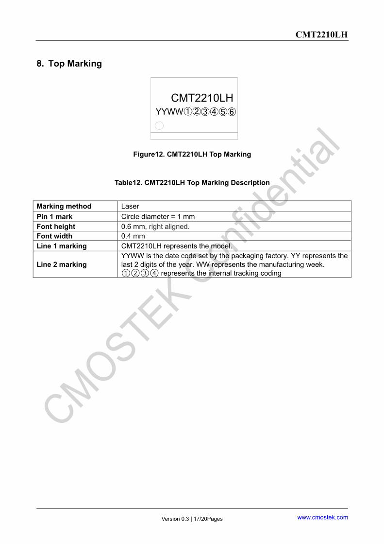
8. Top Marking
①②③④⑤⑥
CMT2210LHYYWW
Figure12. CMT2210LH Top Marking
Table12. CMT2210LH Top Marking Description
Marking method Laser
Pin 1 mark Circle diameter = 1 mm
Font height 0.6 mm, right aligned.
Font width 0.4 mm
Line 1 marking CMT2210LH represents the model.
Line 2 marking
YYWW is the date code set by the packaging factory. YY represents the
last 2 digits of the year. WW represents the manufacturing week.
①②③④ represents the internal tracking coding

CMT2210LH
Version 0.3 | 18/20Pages
www.cmostek.com
9. Other Documents
Table13. CMT2210LH Related Documents
Doc. No. Doc. name Descriptions
AN157 CMT2210LH Configuration
Guideline
Introduce the configuring CMT2210LH details by
RFPDK
AN158 CMT2210LH schematic and
PCB layout guideline
Introduce CMT2210LH schematic and PCB
layout design rules, RF matching network and
other layout considerations. It is the Chinese
version.

CMT2210LH
Version 0.3 | 19/20Pages
www.cmostek.com
10. Document Modification Record
Table14. Document Modification Record Sheet
Version Chapter Modification descriptions Date
0.1 All Initial release version 2017-10-08
0.2 All Fix spelling and grammar mistakes 2017-10-10
0.3 1 Page2,Table1,3.0~5.5V 2018-02-07

CMT2210LH
Version 0.3 | 20/20Pages
www.cmostek.com
11. Contact Information
Wuxi CMOSTEK Microelectronics Co., Ltd. Shenzhen branch
Room 203, Honghai Building, Qianhai Road, Nanshan District, Shenzhen, Guangdong, China
Zip Code: 518000
Tel: +86 - 755 - 83235017
Fax: +86 - 755 - 82761326
Sales: [email protected]
Technical support:[email protected]
Website: www.cmostek.com
The information furnished by CMOSTEK is believed to be accurate and reliable. However, no responsibility is assumed for
inaccuracies and specifications within this document are subject to change without notice. The material contained herein is
the exclusive property of CMOSTEK and shall not be distributed, reproduced, or disclosed in whole or in part without prior
written permission of CMOSTEK. CMOSTEK products are not authorized for use as critical components in life support
devices or systems without express written approval of CMOSTEK. The CMOSTEK logo is a registered trademark of
CMOSTEK Microelectronics Co., Ltd. All other names are the property of their respective owners.
Copyright. CMOSTEK Microelectronics Co., Ltd. All rights are reserved.