CMOS-MEMS for the next generation of “Combo”...
29
The Leader in Motion Interface Solutions September 29, 2012 CMOS-MEMS for the next generation of “Combo” Sensors Stephen Lloyd VP of Engineering InvenSense 1
-
Upload
hoangthuan -
Category
Documents
-
view
217 -
download
2
Transcript of CMOS-MEMS for the next generation of “Combo”...

The Leader in Motion Interface Solutions September 29, 2012
CMOS-MEMS for the next generation of “Combo” Sensors
Stephen Lloyd VP of Engineering InvenSense
1

The Leader in Motion Interface Solutions September 29, 2012
InvenSense Overview
Challenges with MEMS Development
Evolving MEMS Platforms
“Combo” Sensors and MEMS SOC approach
Agenda
2
The Leader in Motion Interface Solutions September 29, 2012
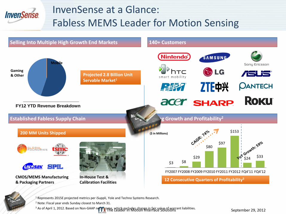
ng Growth and Profitability2 Established Fabless Supply Chain
140+ Customers
InvenSense at a Glance: Fabless MEMS Leader for Motion Sensing
Mobile
Gaming & Other
FY12 YTD Revenue Breakdown
Projected 2.8 Billion Unit Servable Market1
200 MM Units Shipped
Selling Into Multiple High Growth End Markets
12 Consecutive Quarters of Profitability3 In-House Test & Calibration Facilities
CMOS/MEMS Manufacturing & Packaging Partners
($ in Millions)
$3 $8 $29
$80 $97
$153
$24 $33
FY2007 FY2008 FY2009 FY2010 FY2011 FY2012 FQ4'11 FQ4'12
1 Represents 2015E projected metrics per iSuppli, Yole and Techno Systems Research. 2 Note: Fiscal year ends Sunday closest to March 31. 3 As of April 1, 2012. Based on Non-GAAP net income, which excludes change in fair value of warrant liabilities.

The Leader in Motion Interface Solutions September 29, 2012
InvenSense Overview
Challenges with MEMS Development
Evolving MEMS Platforms
“Combo” Sensors and MEMS SOC approach
Agenda
4

The Leader in Motion Interface Solutions September 29, 2012
MEMS vs. CMOS SOC “Micro-Electrical-Mechanical-Systems” • Combination of mechanical and electrical components which
provide a completely functional system We can develop multi-million gate ASIC “Systems”, why is MEMS so challenging? • In CMOS, a large body of proven IP exists along with proven
“SOC” flows which allow rapid development of complex systems. This is the accepted standard for product development. People expect this level of functionality, developed in rapid time frames, and provided at low cost.
The challenges with MEMS product Development
5
The Leader in Motion Interface Solutions September 29, 2012
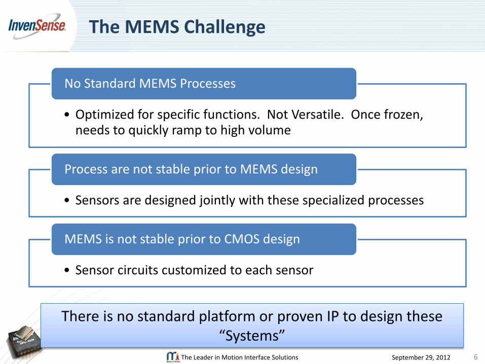
• Optimized for specific functions. Not Versatile. Once frozen, needs to quickly ramp to high volume
No Standard MEMS Processes
• Sensors are designed jointly with these specialized processes
Process are not stable prior to MEMS design
• Sensor circuits customized to each sensor
MEMS is not stable prior to CMOS design
The MEMS Challenge
6
There is no standard platform or proven IP to design these “Systems”
The Leader in Motion Interface Solutions September 29, 2012
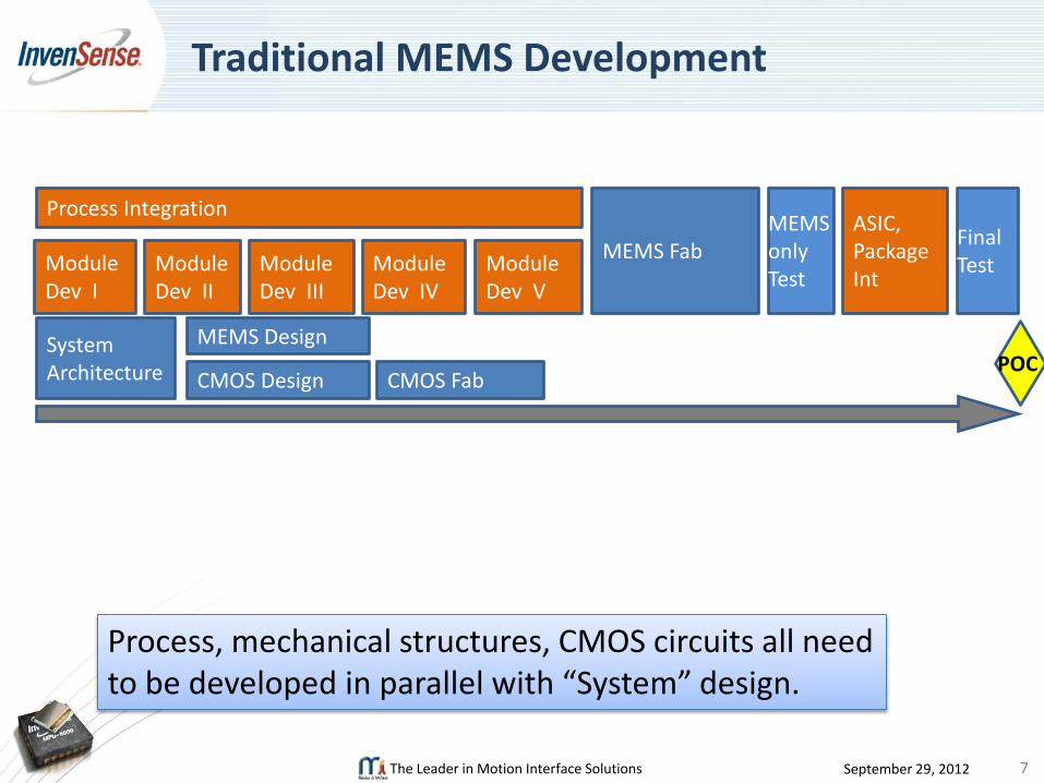
Traditional MEMS Development
MEMS Design
Process Integration MEMS only Test
ASIC, Package Int
Final Test Module
Dev II Module Dev III
Module Dev IV
Module Dev V
Module Dev I
MEMS Fab
CMOS Design CMOS Fab System Architecture
7
POC
Process, mechanical structures, CMOS circuits all need to be developed in parallel with “System” design.

The Leader in Motion Interface Solutions September 29, 2012
Development Challenges
• “One product - one process” increases barrier to entry • Finding foundries capable and willing to develop new process
Process Development
• Difficult to develop a product if the process is not stable • Optimizing both design and process simultaneously • Need for fast design iterations to keep up with market
Product Development
• Over 50% of costs traditionally are in package and test • Need to quickly establish high yield and quality • Consumer products require ability to rapidly scale capacity
Production
8
Expertise and focus are required in all three areas, which can dilute resources.

The Leader in Motion Interface Solutions September 29, 2012
InvenSense Overview
Challenges with MEMS Development
Evolving MEMS Platforms
“Combo” Sensors and MEMS SOC approach
Agenda
9
The Leader in Motion Interface Solutions September 29, 2012
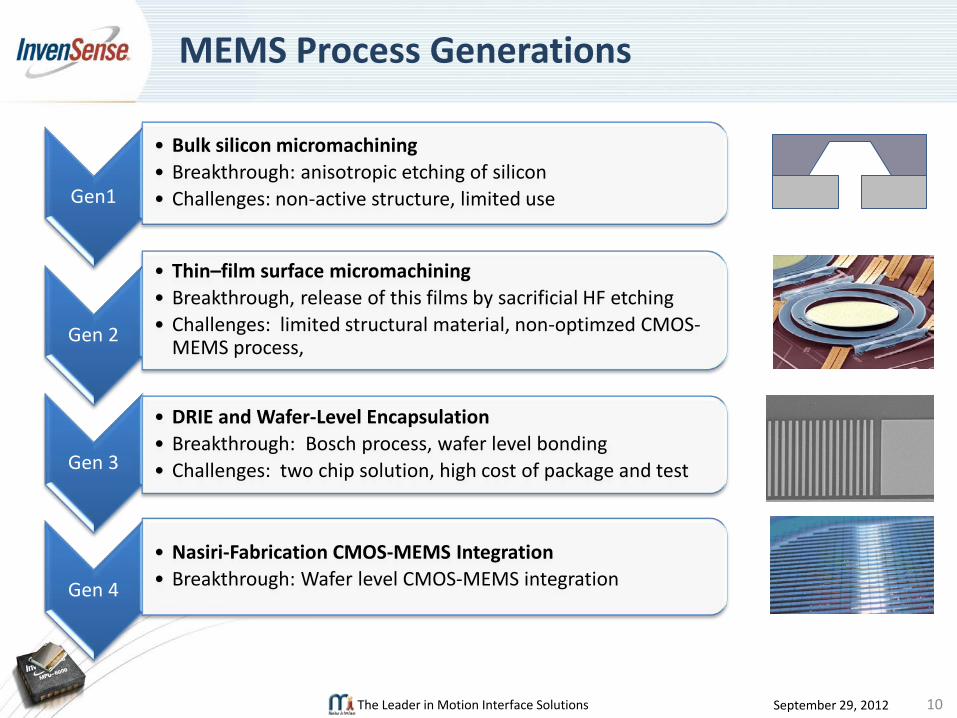
MEMS Process Generations
Gen 2
• Thin–film surface micromachining • Breakthrough, release of this films by sacrificial HF etching • Challenges: limited structural material, non-optimzed CMOS-
MEMS process,
Gen 3
• DRIE and Wafer-Level Encapsulation • Breakthrough: Bosch process, wafer level bonding • Challenges: two chip solution, high cost of package and test
Gen1
• Bulk silicon micromachining • Breakthrough: anisotropic etching of silicon • Challenges: non-active structure, limited use
Gen 4
• Nasiri-Fabrication CMOS-MEMS Integration • Breakthrough: Wafer level CMOS-MEMS integration
10
The Leader in Motion Interface Solutions
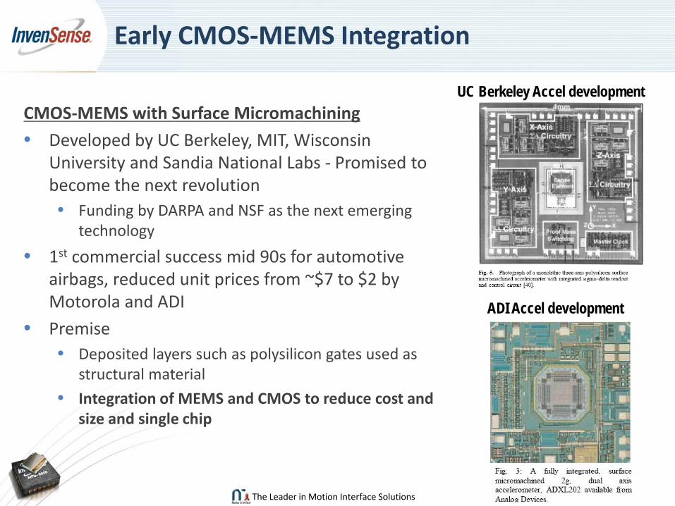
Early CMOS-MEMS Integration
CMOS-MEMS with Surface Micromachining • Developed by UC Berkeley, MIT, Wisconsin
University and Sandia National Labs - Promised to become the next revolution • Funding by DARPA and NSF as the next emerging
technology • 1st commercial success mid 90s for automotive
airbags, reduced unit prices from ~$7 to $2 by Motorola and ADI
• Premise • Deposited layers such as polysilicon gates used as
structural material • Integration of MEMS and CMOS to reduce cost and
size and single chip
C
UC Berkeley Accel development
ADI Accel development
The Leader in Motion Interface Solutions September 29, 2012
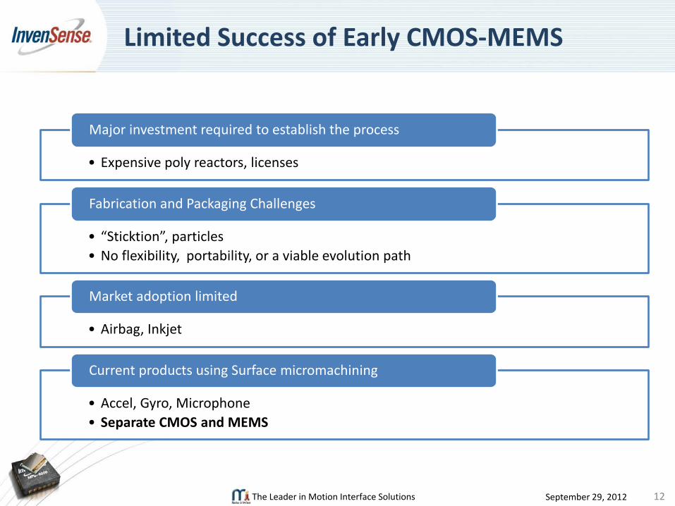
• Expensive poly reactors, licenses
Major investment required to establish the process
• “Sticktion”, particles • No flexibility, portability, or a viable evolution path
Fabrication and Packaging Challenges
• Airbag, Inkjet
Market adoption limited
• Accel, Gyro, Microphone • Separate CMOS and MEMS
Current products using Surface micromachining
Limited Success of Early CMOS-MEMS
12
The Leader in Motion Interface Solutions September 29, 2012
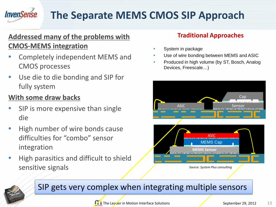
Addressed many of the problems with CMOS-MEMS integration • Completely independent MEMS and
CMOS processes • Use die to die bonding and SIP for
fully system With some draw backs • SIP is more expensive than single
die • High number of wire bonds cause
difficulties for “combo” sensor integration
• High parasitics and difficult to shield sensitive signals
The Separate MEMS CMOS SIP Approach
13
Traditional Approaches
• System in package • Use of wire bonding between MEMS and ASIC • Produced in high volume (by ST, Bosch, Analog
Devices, Freescale…)
MEMS Cap
MEMS Sensor
ASIC
ASIC
Cap
Sensor
Source: System Plus consulting
SIP gets very complex when integrating multiple sensors

The Leader in Motion Interface Solutions September 29, 2012
• People are moving away from optimizing a process for each product
MEMS processes are becoming more capable and multi-purpose
• Key is to be able to use a standard CMOS process with no modification
New approaches to CMOS-MEMS integration
• CMU, Akustica, Baolab, Cavendish Kinetics
Several use the CMOS metal for MEMS structures
• WiSpry
MEMS on top of CMOS
• InvenSense, TSMC
Bonding a MEMS wafer to CMOS
MEMS Process Evolution
14
Ideal Platform: A versatile MEMS process which can be easily combined with standard CMOS processes.
The Leader in Motion Interface Solutions September 29, 2012
InvenSense Overview
Challenges with MEMS Development
Evolving MEMS Platforms
“Combo” Sensors and MEMS SOC approach
Agenda
15

The Leader in Motion Interface Solutions September 29, 2012
~60% Attach Rate for High End SM-Phones With 9-axis Motion Interface
16
1st SM-Phone With 3-axis Accel 2006
Increasing Sensors in Smart Phones

The Leader in Motion Interface Solutions September 29, 2012
• UI’s have evolved from key entry, to touch, motion, and now people are talking about “contextual awareness”
• understand the “context” under which a device is being used. • Availability of low cost sensors help drive this paradigm shift • Expanding variety of MEMS sensors being developed • Examples: light, proximity, inertial, audio, ultra-sonic,
temperature, pressure, humidity, and chemical sensing
Sensor Driver: “Context Aware”
17
As the number of sensors included in a product increases, there is more opportunity to aggregate these sensors into a few products

The Leader in Motion Interface Solutions September 29, 2012
• “We believe that the market for discrete sensors will begin to decline, but the growth for combo solutions will be huge. Though currently less than $100 million niche, we expect combos to be a $1.7 billion opportunity by 2017”*
“Combo” Sensor Integration is a Growing Trend
18
*I-Micronews: 2012 Status of MEMS Industry, Yole Devel. And MIG, Abstract

The Leader in Motion Interface Solutions September 29, 2012
2002-2005 2006-2009 2010 2011 2012
MPU-6050 6-Axis
4x4x0.9mm
MPU-9250 9-Axis
3x3x1mm
3-axis compass 3x3x1.4 mm
2-axis gyro 6x6x1.4mm
3-axis Accel 4x4x1.45 mm
Evolution of Motion Sensors to MotionTracking
1-axis 7x12x2.6 mm
3-axis compass: X/Y: 3x3x1mm Z: 10x1.4x3.9
3-axis Accel 5x5x1.8mm
Motion Sensors
MPU-6500 6-Axis
3x3x0.9mm
Integrated MotionTracking 2-axis Gyro
4x5x1.2mm
3-axis compass 4x4x0.7 mm
3-axis Accel 3x3x1 mm
3-axis Gyro 4x4x0.9mm
3-axis Accel 2x2x1 mm
3-axis compass 2x2x0.7 mm

The Leader in Motion Interface Solutions September 29, 2012
• Smaller die due to shared circuits
Cost
• Single die package smaller than SIP packages
Size
• Share bias, digital current across multiple sensors
Power
• Low parasitic connections • Leverage a “system” approach with multiple sensors
Performance
Advantages of “Combo” Sensor Integration
20

The Leader in Motion Interface Solutions September 29, 2012
Example of “Combo” Sensor Integration
SIP 6-axis Solution
Integrated 6-axis Solution (MPU-6500 model)
Package Size • 3x3x0.9mm, single die • 5x4x1.1mm, 4 die
Components • 3-Axis Accelerometer • 3-Axis Gyroscope • Digital Motion Processing (DMP) Engine
• Accelerometer • 3-Axis Gyroscope
Sensor Fusion
• Single I2C or SPI output • Single 6-axis Sensor Fusion
• Two separate I2C outputs
Cost • Low cost QFN • High cost Multi-chip LGA
Source: STMicro company website and “MEMS on Silicon” presentation, Sept 29, 2011. Note: Competing 6-axis solution statistics are for STMicro’s LSM330DL model.
gyro accel
gyro accel
The Leader in Motion Interface Solutions September 29, 2012
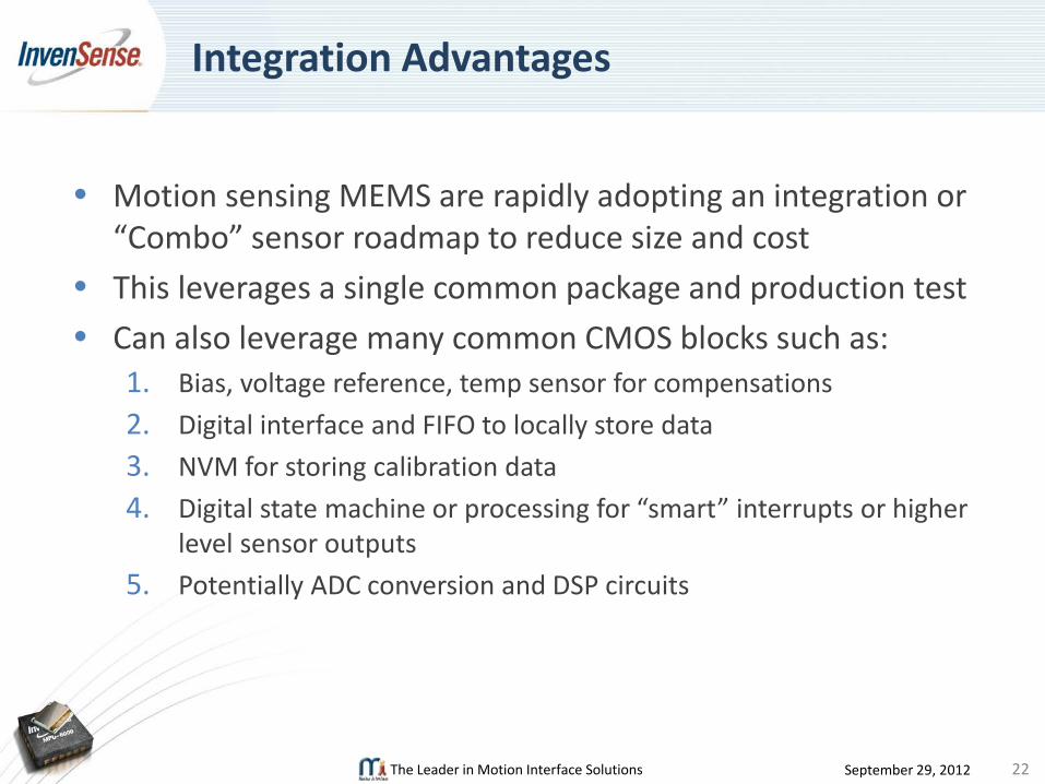
• Motion sensing MEMS are rapidly adopting an integration or “Combo” sensor roadmap to reduce size and cost
• This leverages a single common package and production test • Can also leverage many common CMOS blocks such as:
1. Bias, voltage reference, temp sensor for compensations 2. Digital interface and FIFO to locally store data 3. NVM for storing calibration data 4. Digital state machine or processing for “smart” interrupts or higher
level sensor outputs 5. Potentially ADC conversion and DSP circuits
Integration Advantages
22

The Leader in Motion Interface Solutions September 29, 2012
Most MEMS Sensors standardizing on I2C
Even a simple feature such as a digital interface adds extra circuitry and cost which can be shared as additional sensors are integrated

The Leader in Motion Interface Solutions September 29, 2012
Individual sensors
• Lowest level, but can provide built in intelligence to lower system power and embed sensor expertise.
• Low power consumption, so many sensors can stay active for long periods of time
Sensor Hub
• Aggregates sensor inputs, can provide some information processing to determine if the AP should be woken up
• Uses less power than the AP, signal processing can be shared across all sensors.
Application Processor
• Used for the “heavy lifting” in processing the sensor data and enabling applications.
• Uses the most power when active. Needs to be able to sleep for long periods of time when the system is idle to save power.
Hierarchy for Mobile Sensor Integration
24
MEMS SOC approach: sensors and hub can be integrated into a single product
The Leader in Motion Interface Solutions September 29, 2012
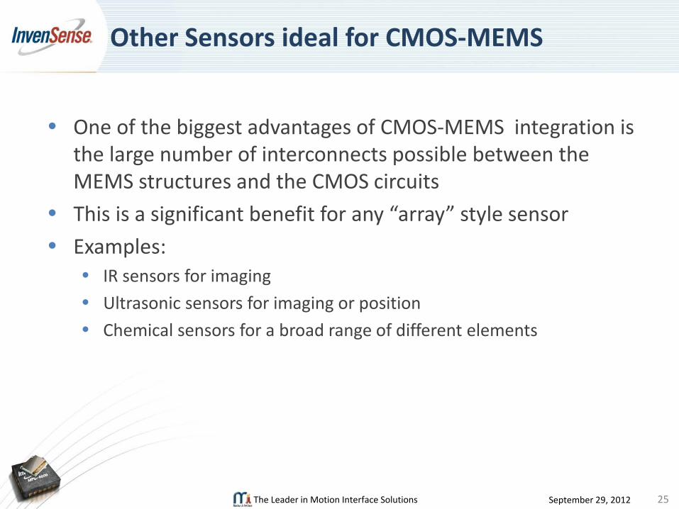
• One of the biggest advantages of CMOS-MEMS integration is the large number of interconnects possible between the MEMS structures and the CMOS circuits
• This is a significant benefit for any “array” style sensor • Examples:
• IR sensors for imaging • Ultrasonic sensors for imaging or position • Chemical sensors for a broad range of different elements
Other Sensors ideal for CMOS-MEMS
25

The Leader in Motion Interface Solutions September 29, 2012
Widening MEMS Sensor Applications
Imaging Gaming
SmartPhone Toys
Tablets
Smart TV
Navigation
Sport & Fitness
Appliance
Health Monitoring
>3 B
U
2010 2012 2014 2008

The Leader in Motion Interface Solutions September 29, 2012
• Foundries now offer CMOS-MEMS Platforms • Greatly simplifies MEMS product development • Stable Process which can quickly ramp to high volume
• Companies can now focus all their resources on the MEMS
structures and overall system design
The Availability of CMOS-MEMS Platforms
27
This should significantly reduce the challenges for new MEMS start-ups and help create a wave of new, innovative sensors
The Leader in Motion Interface Solutions September 29, 2012
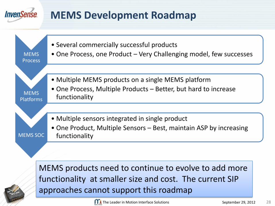
MEMS Process
• Several commercially successful products • One Process, one Product – Very Challenging model, few successes
MEMS Platforms
• Multiple MEMS products on a single MEMS platform • One Process, Multiple Products – Better, but hard to increase
functionality
MEMS SOC
• Multiple sensors integrated in single product • One Product, Multiple Sensors – Best, maintain ASP by increasing
functionality
MEMS Development Roadmap
28
MEMS products need to continue to evolve to add more functionality at smaller size and cost. The current SIP approaches cannot support this roadmap