Cmos fabrication video Tirumala engineering college
48
1 Lecture 5: IC Fabrication The Transistor Revolution First transistor Bell Labs, 1948 baey: Digital Integrated Circuits 2nd
-
Upload
bhagi-sitarama-sireesha -
Category
Technology
-
view
173 -
download
2
Transcript of Cmos fabrication video Tirumala engineering college
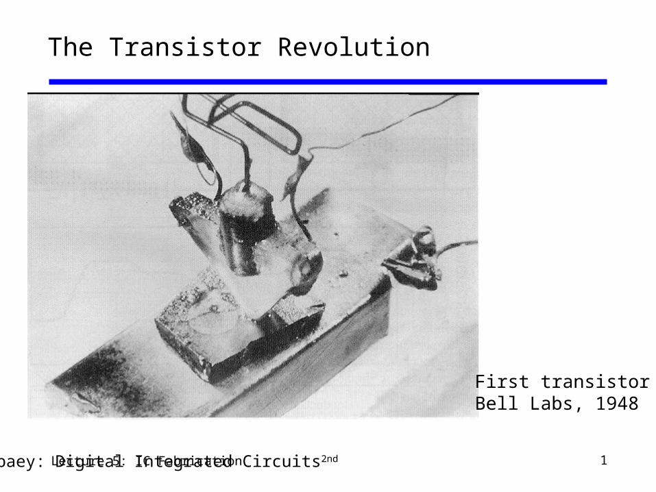
1Lecture 5: IC Fabrication
The Transistor Revolution
First transistorBell Labs, 1948
© Rabaey: Digital Integrated Circuits2nd
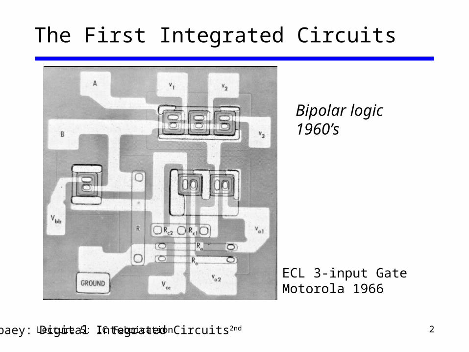
2Lecture 5: IC Fabrication
The First Integrated Circuits
Bipolar logic1960’s
ECL 3-input GateMotorola 1966
© Rabaey: Digital Integrated Circuits2nd
3Lecture 5: IC Fabrication
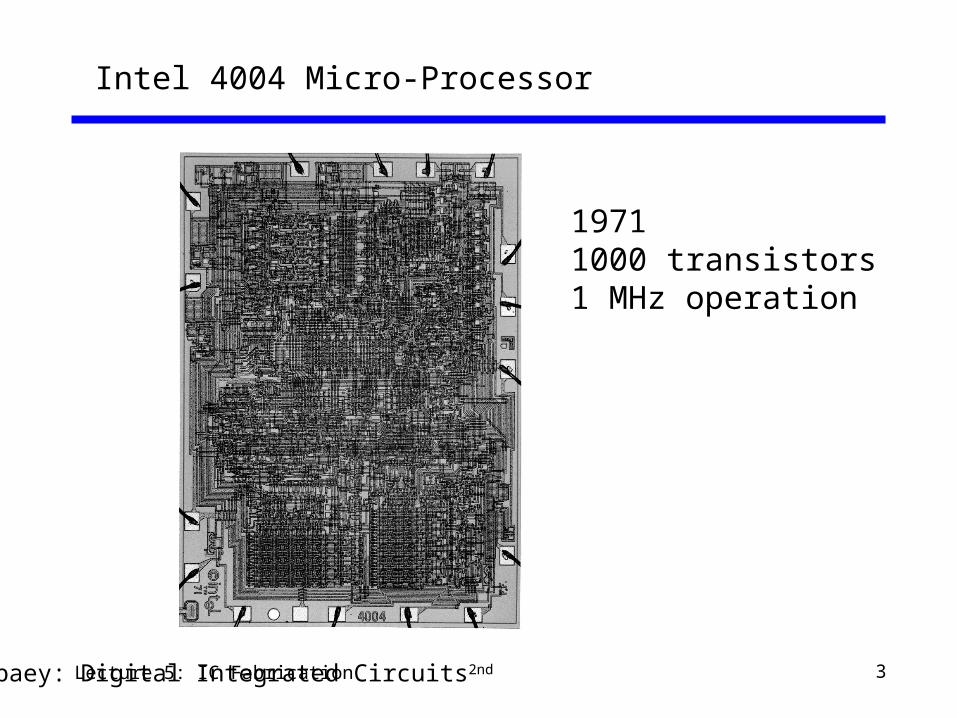
Intel 4004 Micro-Processor
19711000 transistors1 MHz operation
© Rabaey: Digital Integrated Circuits2nd
4Lecture 5: IC Fabrication
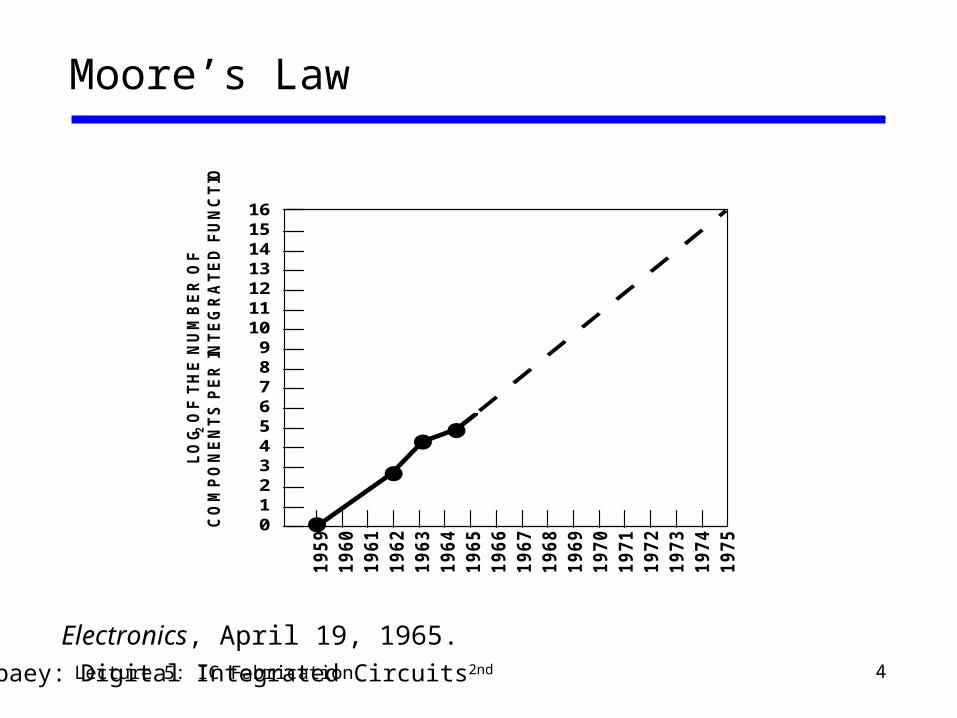
Moore’s Law
161514131211109876543210
195
9
196
0
196
1
196
2
196
3
196
4
196
5
196
6
196
7
196
8
196
9
197
0
197
1
197
2
197
3
197
4
197
5
LO
G 2 O
F T
HE
NU
MB
ER
OF
CO
MP
ON
EN
TS
PE
R I
NT
EG
RA
TE
D F
UN
CT
ION
Electronics, April 19, 1965.© Rabaey: Digital Integrated Circuits2nd
5Lecture 5: IC Fabrication
Silicon IC processing
Similar to photographic printing Expose the silicon wafer through a mask Process the silicon wafer Repeat sequentially to pattern all the layers
Layout: A set of masks that tell a fabricator what to pattern For each layer in your circuit Layers are metal, drain/source implants, gate, etc. You draw the layers
Subject to vendor-supplied spacing rules
6Lecture 5: IC Fabrication
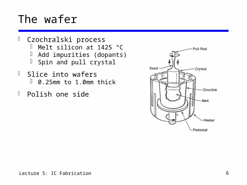
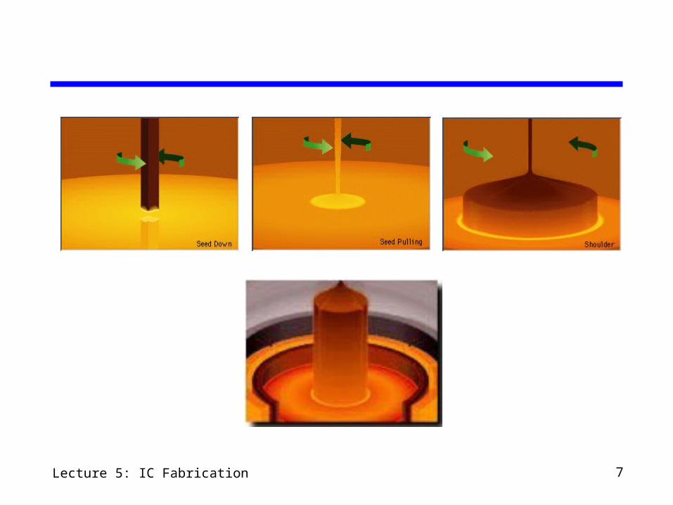
The wafer
Czochralski process Melt silicon at 1425 °C Add impurities (dopants) Spin and pull crystal
Slice into wafers 0.25mm to 1.0mm thick
Polish one side
7Lecture 5: IC Fabrication
8Lecture 5: IC Fabrication
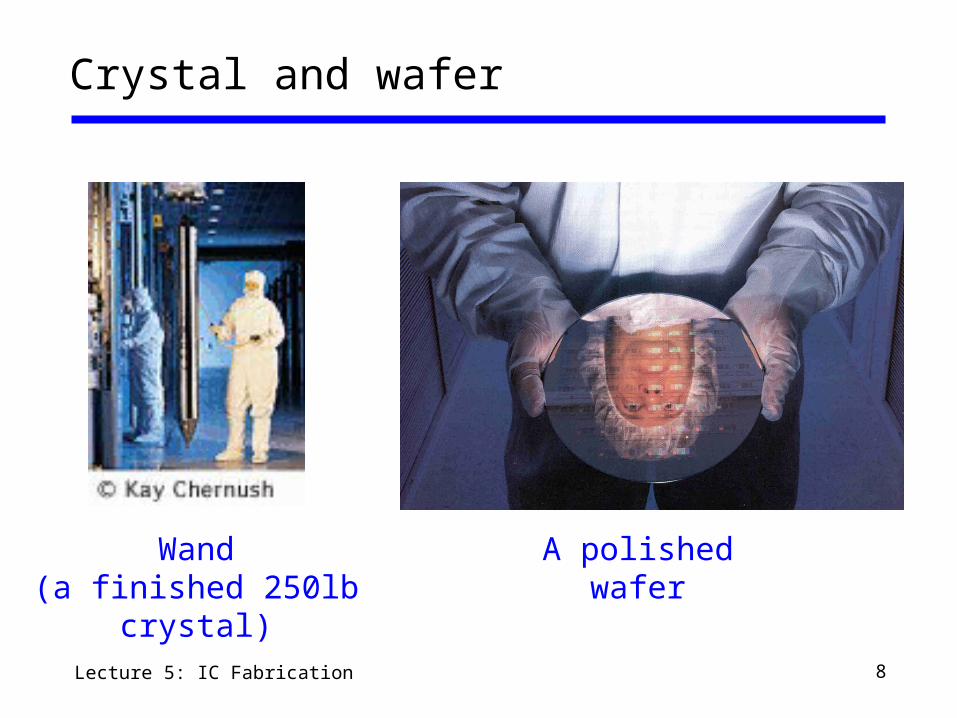
Crystal and wafer
Wand(a finished 250lb crystal)
A polished wafer
9Lecture 5: IC Fabrication
4X reticle
Wafer
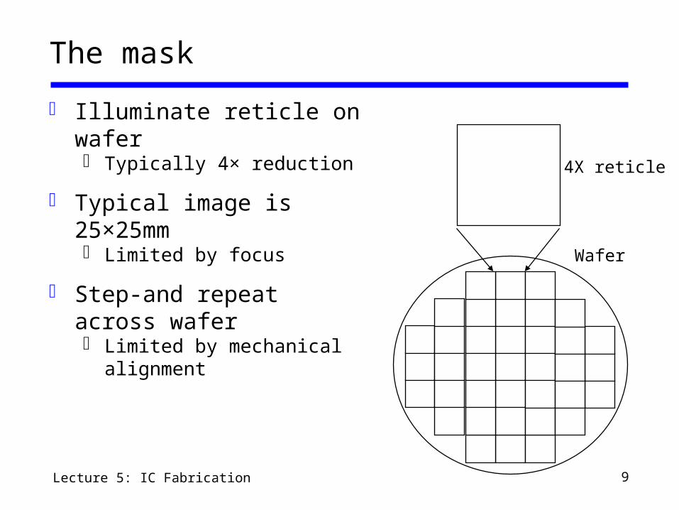
The mask
Illuminate reticle on wafer Typically 4× reduction
Typical image is 25×25mm Limited by focus
Step-and repeat across wafer Limited by mechanical
alignment
10Lecture 5: IC Fabrication Reference: FULLMAN KINETICS
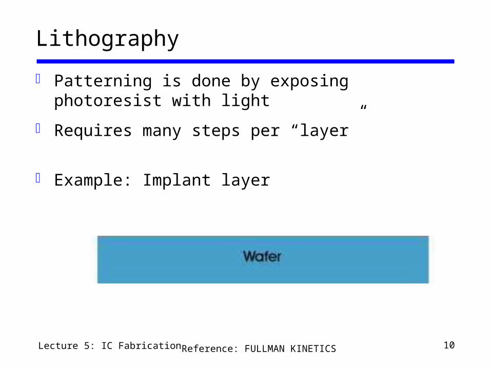
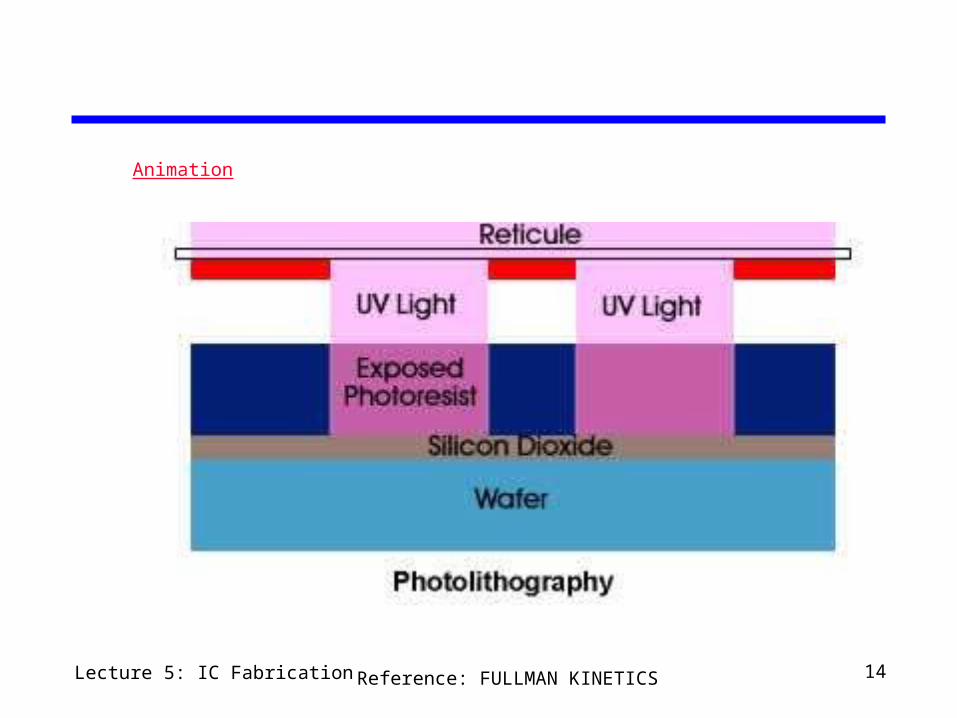
Lithography
Patterning is done by exposing photoresist with light
Requires many steps per “layer”
Example: Implant layer
11Lecture 5: IC Fabrication
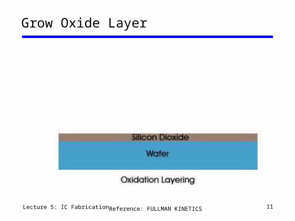
Grow Oxide Layer
Reference: FULLMAN KINETICS
12Lecture 5: IC Fabrication Reference: FULLMAN KINETICS
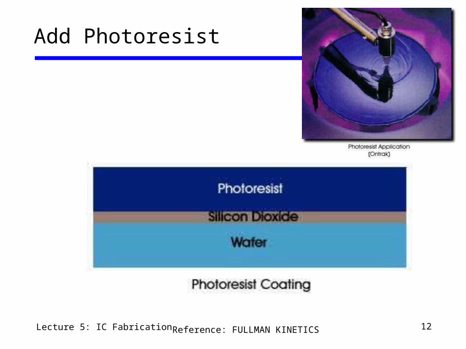
Add Photoresist
13Lecture 5: IC Fabrication Reference: FULLMAN KINETICS
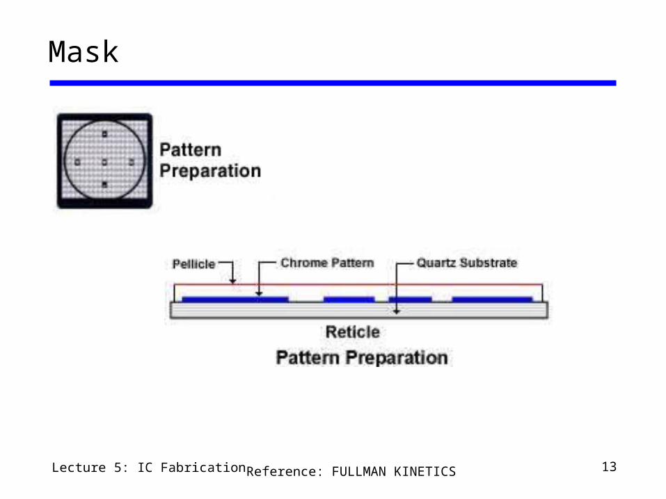
Mask
14Lecture 5: IC Fabrication Reference: FULLMAN KINETICS
Animation
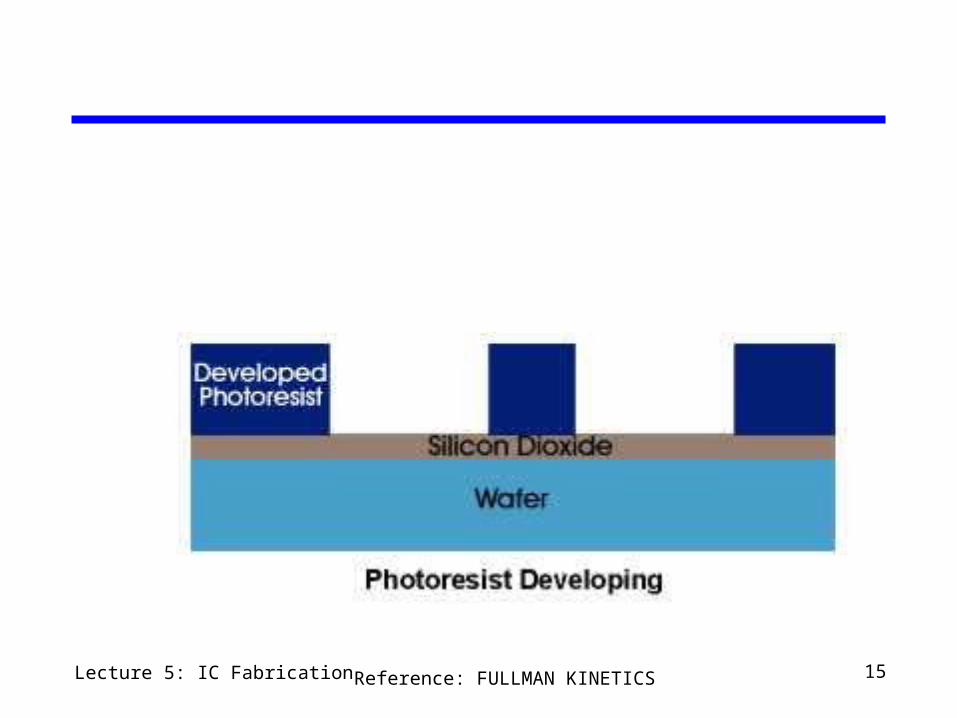
15Lecture 5: IC Fabrication Reference: FULLMAN KINETICS
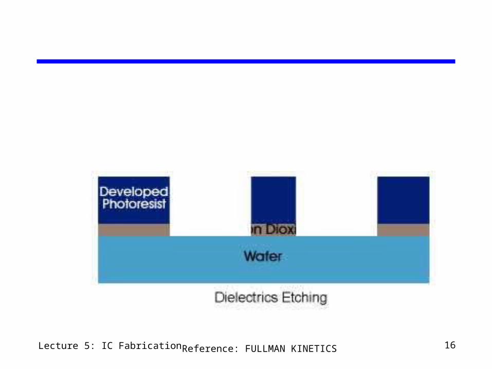
16Lecture 5: IC Fabrication Reference: FULLMAN KINETICS
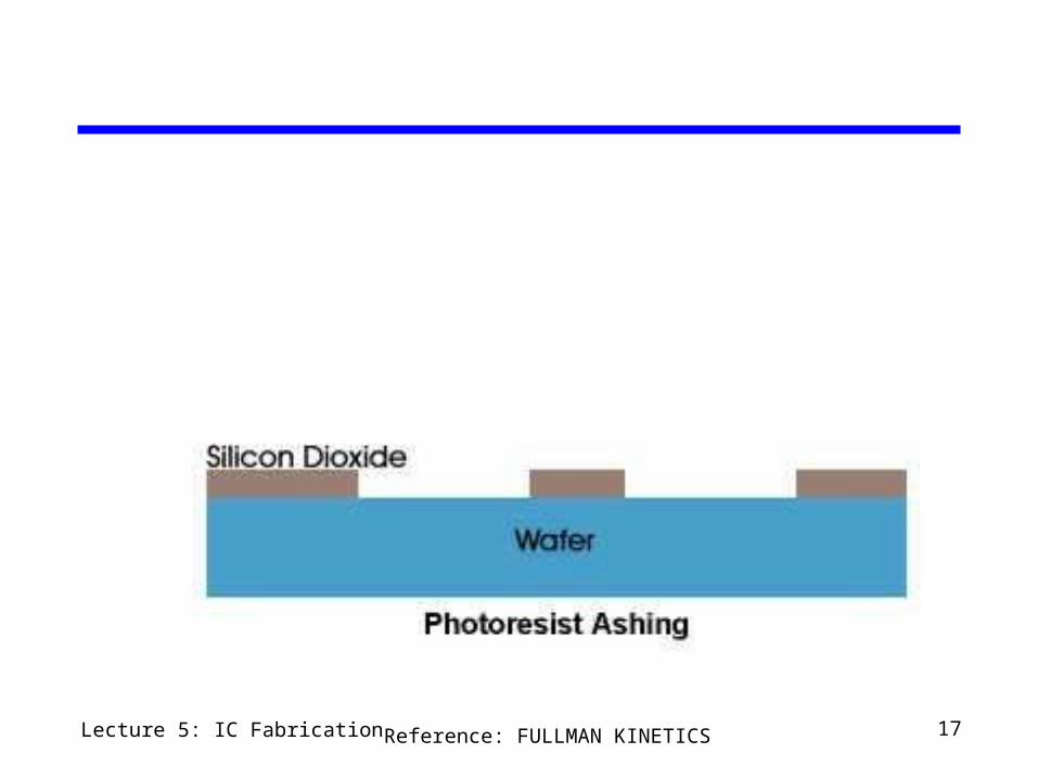
17Lecture 5: IC Fabrication Reference: FULLMAN KINETICS
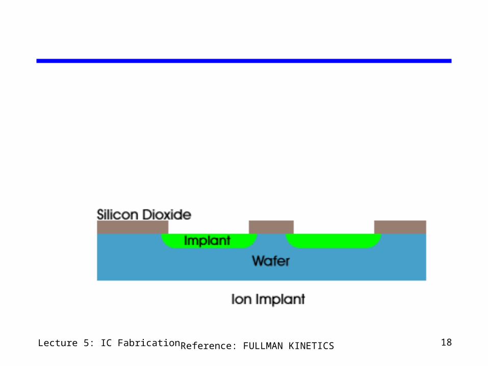
18Lecture 5: IC Fabrication Reference: FULLMAN KINETICS
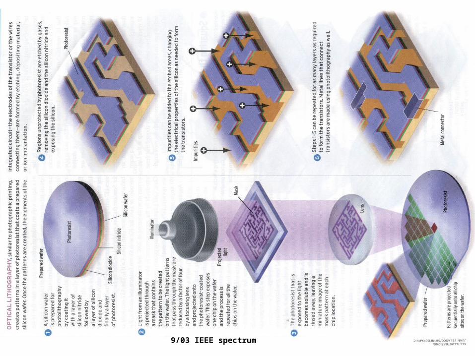
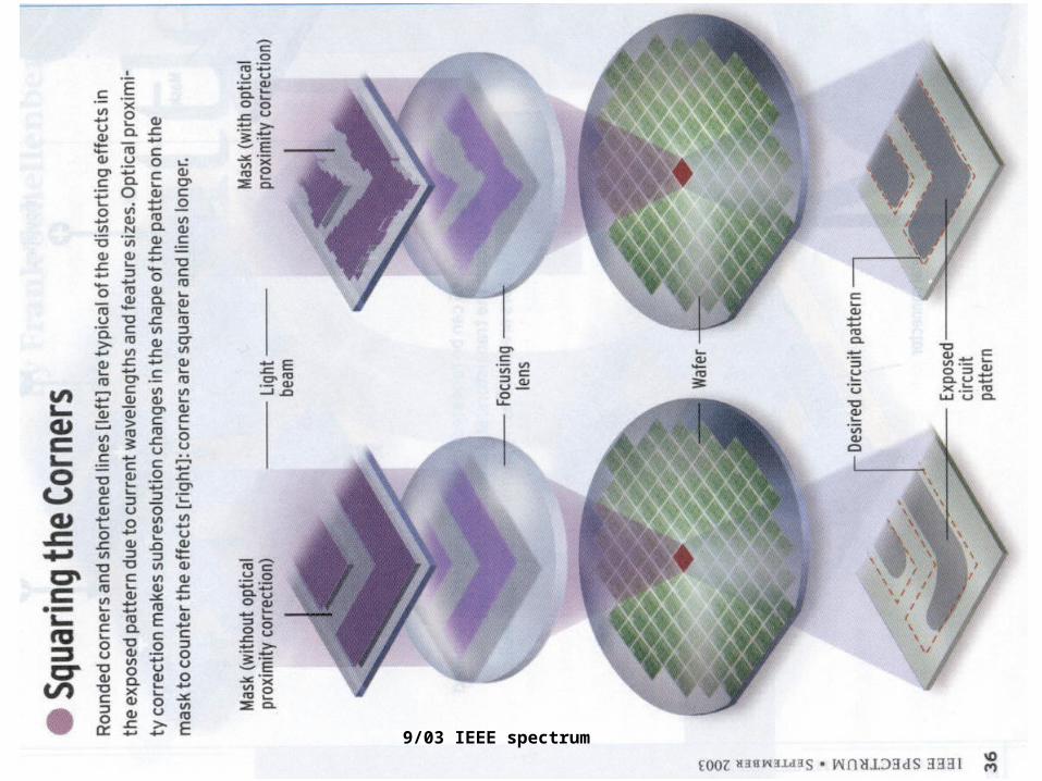
19Lecture 5: IC Fabrication9/03 IEEE spectrum
20Lecture 5: IC Fabrication
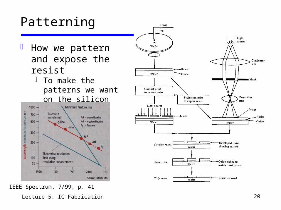
Patterning
How we pattern and expose the resist To make the
patterns we want on the silicon
IEEE Spectrum, 7/99, p. 41
21Lecture 5: IC Fabrication 9/03 IEEE spectrum
22Lecture 5: IC Fabrication
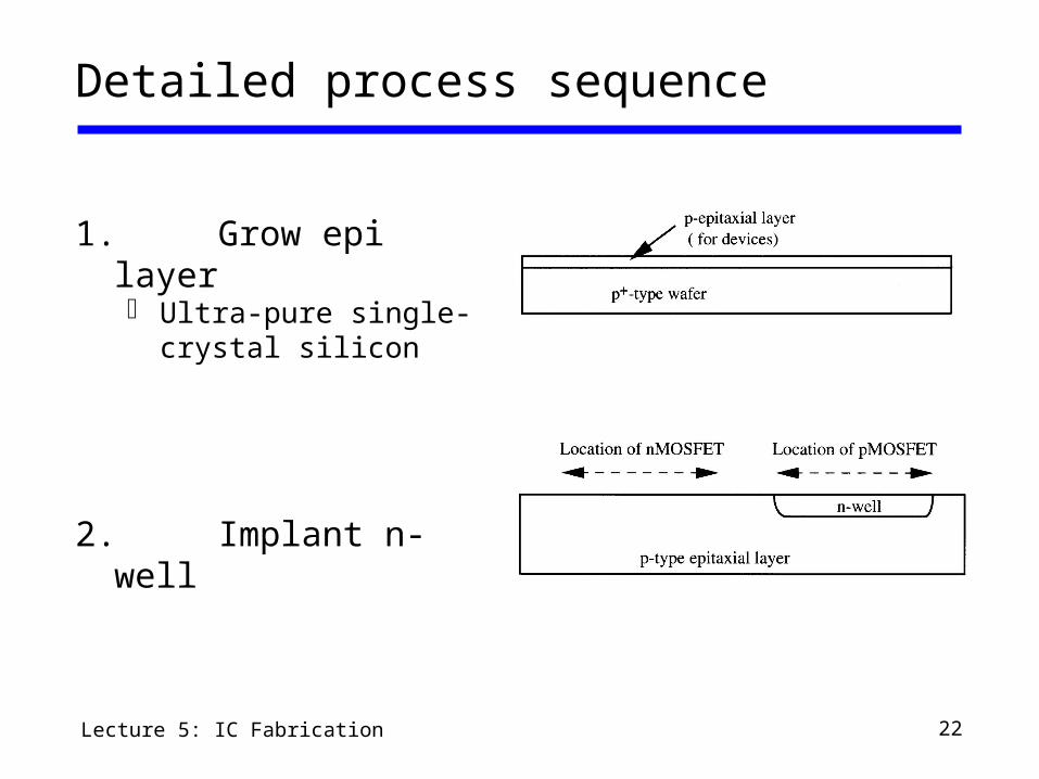
Detailed process sequence
1. Grow epi layer Ultra-pure single-
crystal silicon
2. Implant n-well
23Lecture 5: IC Fabrication
Detailed process sequence (con’t)
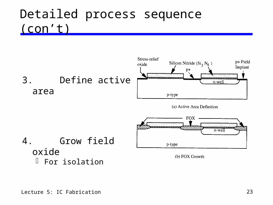
3. Define active area
4. Grow field oxide For isolation
24Lecture 5: IC Fabrication
Detailed process sequence (con’t)
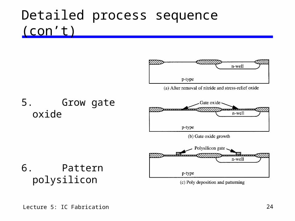
5. Grow gate oxide
6. Pattern polysilicon
25Lecture 5: IC Fabrication
Detailed process sequence (con’t)
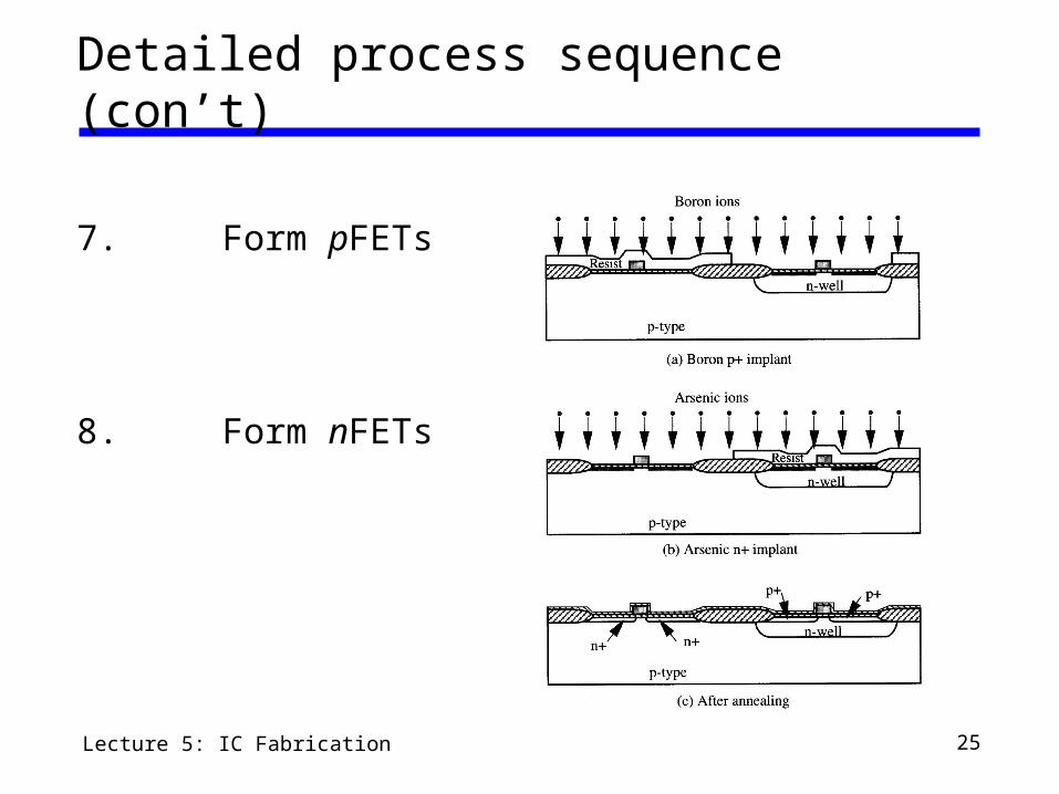
7. Form pFETs
8. Form nFETs
26Lecture 5: IC Fabrication
Detailed process sequence (con’t)
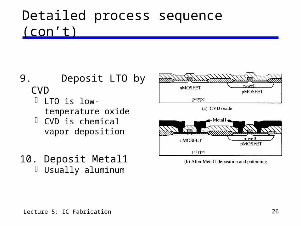
9. Deposit LTO by CVD LTO is low-temperature
oxide CVD is chemical vapor
deposition
10. Deposit Metal1 Usually aluminum
27Lecture 5: IC Fabrication
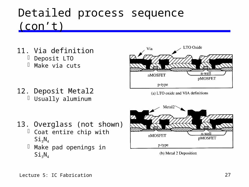
Detailed process sequence (con’t)
11. Via definition Deposit LTO Make via cuts
12. Deposit Metal2 Usually aluminum
13. Overglass (not shown) Coat entire chip with Si3N4
Make pad openings in Si3N4
28Lecture 5: IC Fabrication
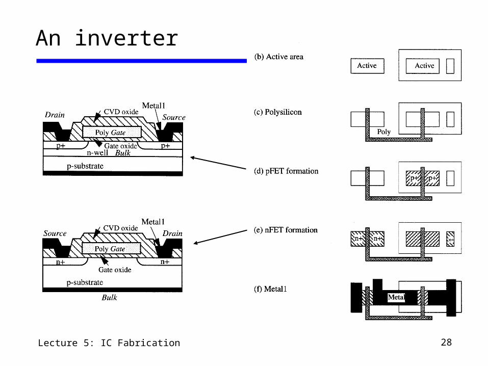
An inverter
29Lecture 5: IC Fabrication
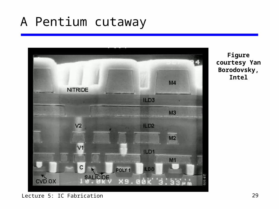
Figure courtesy Yan Borodovsky,
Intel
A Pentium cutaway
30Lecture 5: IC Fabrication
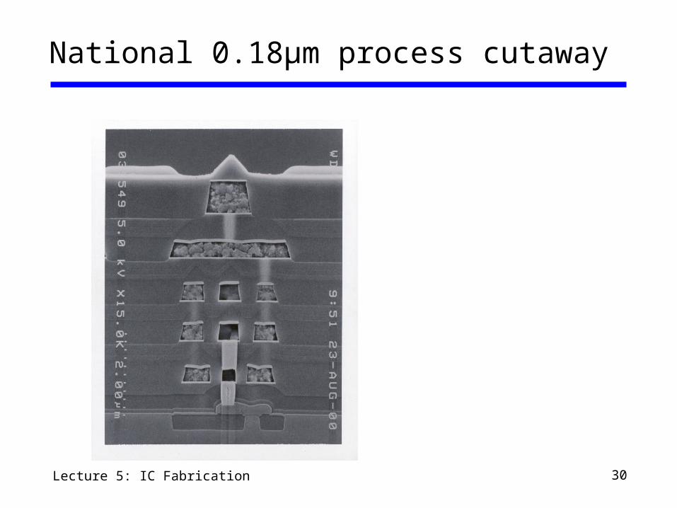
National 0.18µm process cutaway
31Lecture 5: IC Fabrication
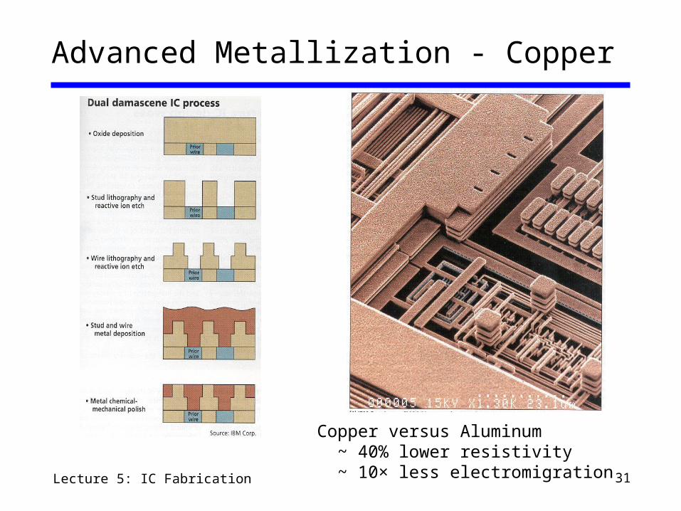
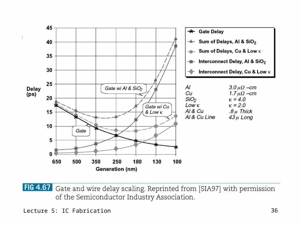
Advanced Metallization - Copper
Copper versus Aluminum ~ 40% lower resistivity ~ 10× less electromigration
32Lecture 5: IC Fabrication
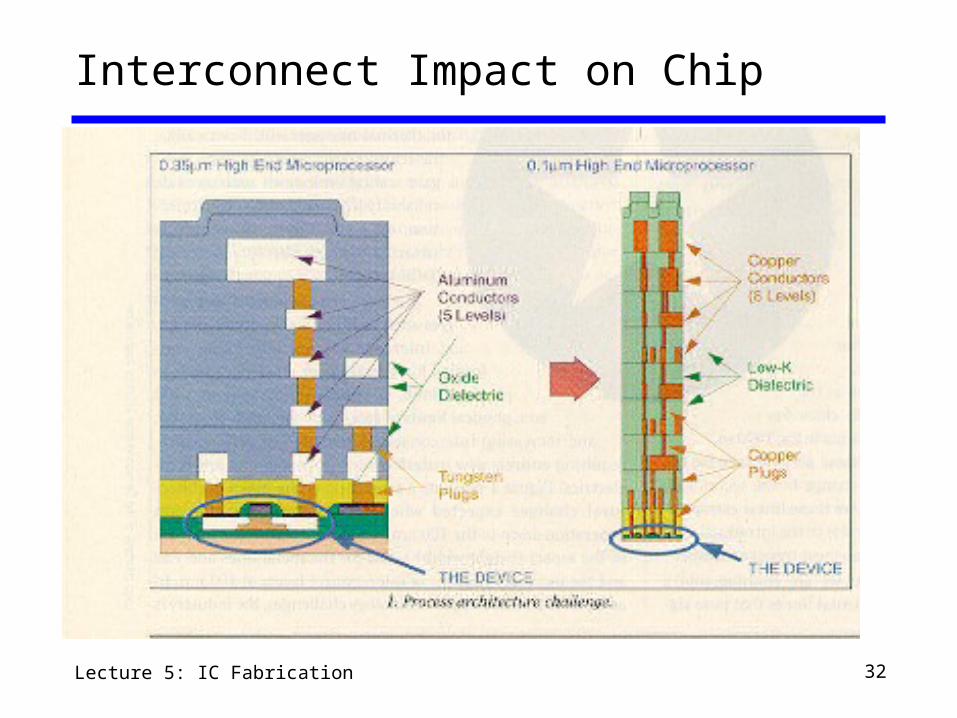
Interconnect Impact on Chip
33Lecture 5: IC Fabrication
10 100 1,000 10,000 100,000
Length (u)
No
of
ne
ts(L
og
Sc
ale
)
Pentium Pro (R)
Pentium(R) II
Pentium (MMX)
Pentium (R)
Pentium (R) II
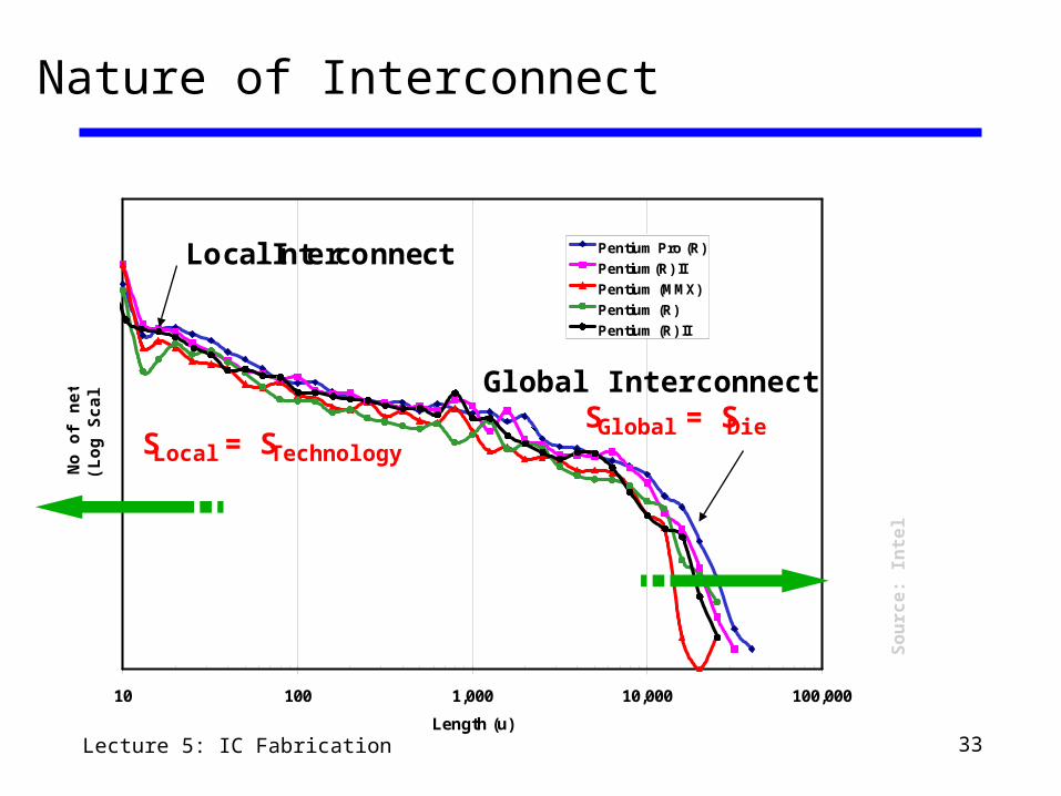
Nature of Interconnect
Local Interconnect
Global Interconnect
SLocal = STechnology
SGlobal = SDie
So
urc
e:
Inte
l
34Lecture 5: IC Fabrication
35Lecture 5: IC Fabrication
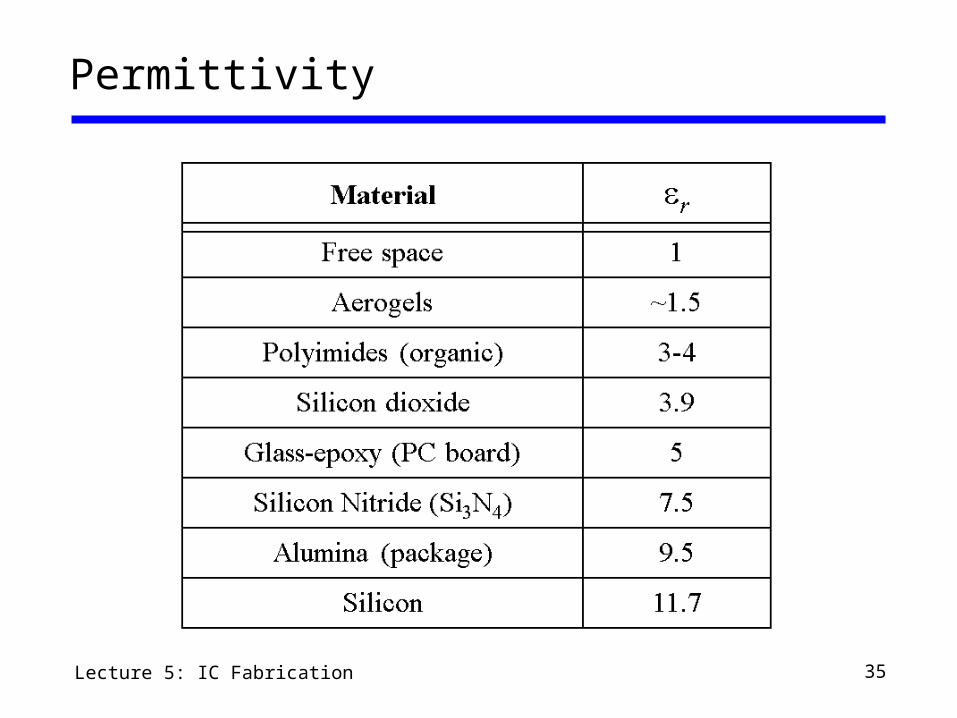
Permittivity
36Lecture 5: IC Fabrication
37Lecture 5: IC Fabrication
38Lecture 5: IC Fabrication
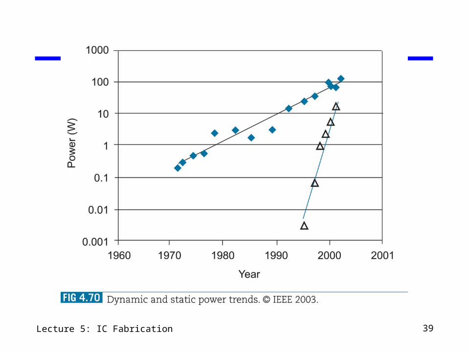
39Lecture 5: IC Fabrication
40Lecture 5: IC Fabrication
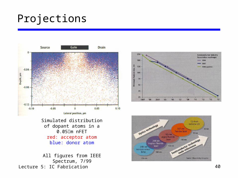
Projections
Simulated distribution of dopant atoms in a 0.05m nFET
red: acceptor atomblue: donor atom
All figures from IEEE Spectrum, 7/99
41Lecture 5: IC Fabrication
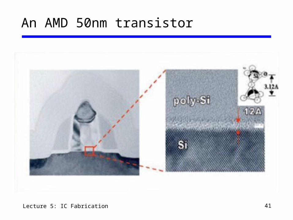
An AMD 50nm transistor
42Lecture 5: IC Fabrication
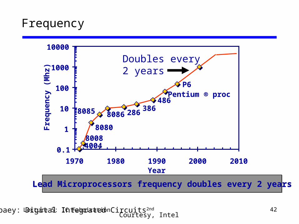
Frequency
P6Pentium ® proc
486386
28680868085
8080
80084004
0.1
1
10
100
1000
10000
1970 1980 1990 2000 2010Year
Fre
qu
ency
(M
hz)
Lead Microprocessors frequency doubles every 2 yearsLead Microprocessors frequency doubles every 2 years
Doubles every2 years
Courtesy, Intel© Rabaey: Digital Integrated Circuits2nd
43Lecture 5: IC Fabrication
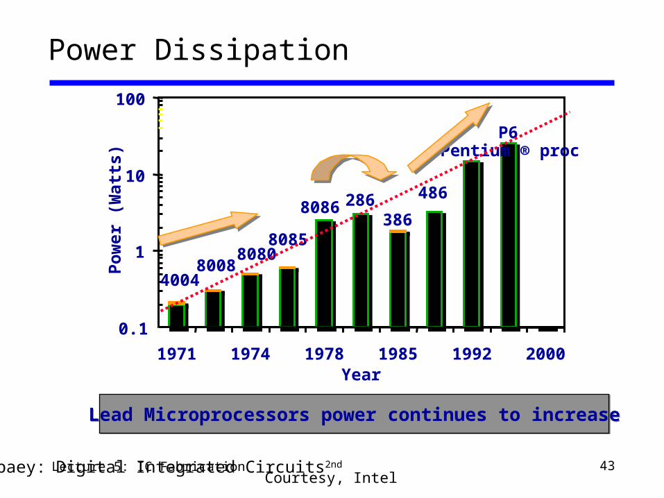
Power Dissipation
P6Pentium ® proc
486
3862868086
80858080
80084004
0.1
1
10
100
1971 1974 1978 1985 1992 2000Year
Po
wer
(W
atts
)
Lead Microprocessors power continues to increaseLead Microprocessors power continues to increase
Courtesy, Intel© Rabaey: Digital Integrated Circuits2nd
44Lecture 5: IC Fabrication
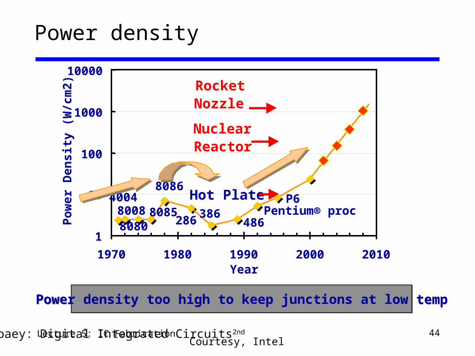
Power density
400480088080
8085
8086
286386
486Pentium® proc
P6
1
10
100
1000
10000
1970 1980 1990 2000 2010Year
Po
wer
Den
sity
(W
/cm
2)
Hot Plate
NuclearReactor
RocketNozzle
Power density too high to keep junctions at low tempPower density too high to keep junctions at low temp
Courtesy, Intel© Rabaey: Digital Integrated Circuits2nd
45Lecture 5: IC Fabrication
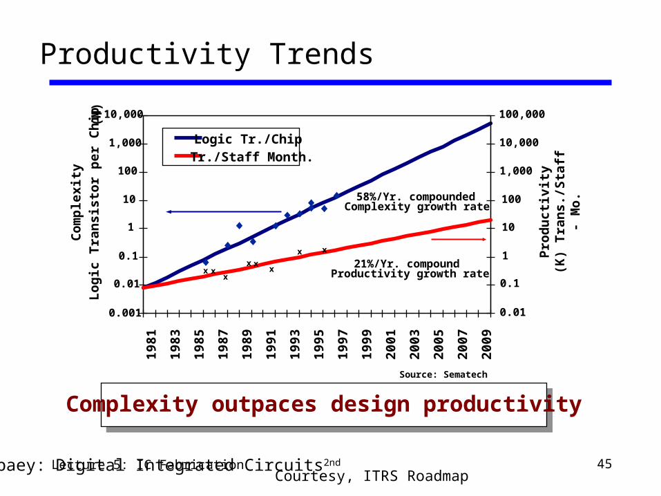
Productivity Trends
1
10
100
1,000
10,000
100,000
1,000,000
10,000,000
200
3
198
1
198
3
198
5
198
7
198
9
199
1
199
3
199
5
199
7
199
9
200
1
200
5
200
7
200
9
10
100
1,000
10,000
100,000
1,000,000
10,000,000
100,000,000
Logic Tr./ChipTr./Staff Month.
xxx
xxx
x
21%/Yr. compoundProductivity growth rate
x
58%/Yr. compoundedComplexity growth rate
10,000
1,000
100
10
1
0.1
0.01
0.001
Lo
gic
Tra
nsi
sto
r p
er C
hip
(M)
0.01
0.1
1
10
100
1,000
10,000
100,000
Pro
du
ctiv
ity
(K)
Tra
ns.
/Sta
ff -
Mo
.
Source: Sematech
Complexity outpaces design productivity
Co
mp
lexi
ty
Courtesy, ITRS Roadmap© Rabaey: Digital Integrated Circuits2nd
46Lecture 5: IC Fabrication
Cost of Integrated Circuits
NRE (non-recurrent engineering) costs design time and effort, mask generation one-time cost factor
Recurrent costs silicon processing, packaging, test proportional to volume proportional to chip area
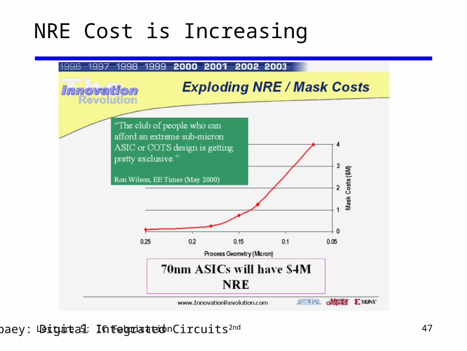
47Lecture 5: IC Fabrication
NRE Cost is Increasing
© Rabaey: Digital Integrated Circuits2nd
48Lecture 5: IC Fabrication
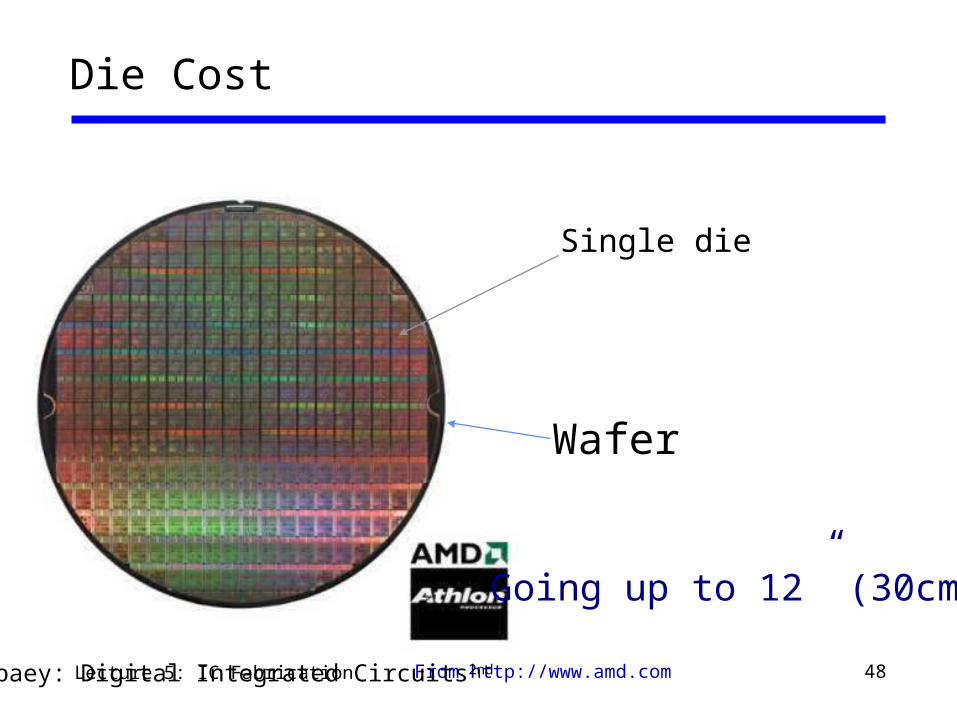
Die Cost
Single die
Wafer
From http://www.amd.com
Going up to 12” (30cm)
© Rabaey: Digital Integrated Circuits2nd