CMOS Digital Integrated Circuits 1 Lec 12 Dynamic Logic Circuits.
61
CMOS Digital Integrated Circuits 1 CMOS Digital Integrated Circuits Lec 12 Dynamic Logic Circuits
-
Upload
simon-williamson -
Category
Documents
-
view
278 -
download
16
Transcript of CMOS Digital Integrated Circuits 1 Lec 12 Dynamic Logic Circuits.

CMOS Digital Integrated Circuits1
CMOS Digital Integrated Circuits
Lec 12
Dynamic Logic Circuits
CMOS Digital Integrated Circuits2
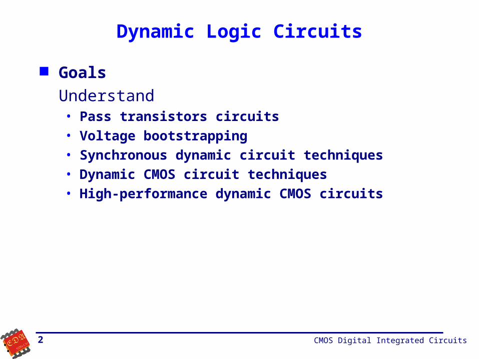
Dynamic Logic Circuits
Goals
Understand• Pass transistors circuits
• Voltage bootstrapping
• Synchronous dynamic circuit techniques
• Dynamic CMOS circuit techniques
• High-performance dynamic CMOS circuits

CMOS Digital Integrated Circuits3
Static v.s. Dynamic
Static Logic Gates• Valid logic levels are steady-state operating points
• Outputs are generated in response to input voltage levels after a certain time delay, and it can preserve its output levels as long as there is power.
• All gate output nodes have a conducting path to VDD or GND, except when input changes are occurring.
Dynamic Logic Gates• The operation depends on temporary storage of charge in parasitic
node capacitances.
• The stored charge does not remain indefinitely, so must be updated or refreshed. This requires establishment of an update or recharge path to the capacitance frequently enough to preserve valid voltage levels.

CMOS Digital Integrated Circuits4
Static v.s. Dynamic (Continued)
Advantages of Dynamic Logic Gates• Allow implementation of simple sequential circuits with memory
functions.
• Use of common clock signals throughout the system enables the synchronization of various circuit blocks.
• Implementation of complex circuits requires a smaller silicon area than static circuits.
• Often consumes less dynamic power than static designs, due to smaller parasitic capacitances.

CMOS Digital Integrated Circuits5
Pass-Transistor LatchCircuit and Operation
Operation• CK = H, D=H or L : CX is charged up or down through MP, and X
becomes H or L (depends on D input) since MP is on D and X are connected.
• CK = L: X is unchanged since MP is off and CX is isolated from D, and the charge is stored on capacitances CX.
• For X = H, Q = L and Q = H
• For X = L, Q = H and Q = L
Cost: 3 to 5 devices (very low)
MP
CKCx
D VxML
MD
Q Q
Soft note
X
CMOS Digital Integrated Circuits6
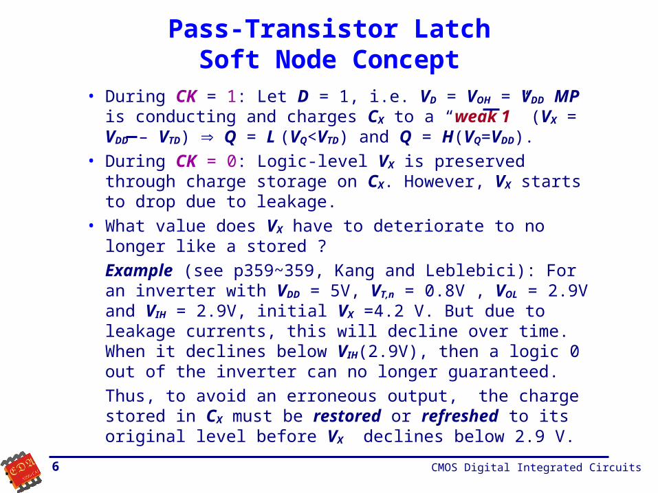
Pass-Transistor LatchSoft Node Concept
• During CK = 1: Let D = 1, i.e. VD = VOH = VDD MP is conducting and charges CX to a “weak 1” (VX = VDD – VTD) Q = L (VQ<VTD) and Q = H(VQ=VDD).
• During CK = 0: Logic-level VX is preserved through charge storage on CX. However, VX starts to drop due to leakage.
• What value does VX have to deteriorate to no longer like a stored ?
Example (see p359~359, Kang and Leblebici): For an inverter with VDD = 5V, VT,n = 0.8V , VOL = 2.9V and VIH = 2.9V, initial VX =4.2 V. But due to leakage currents, this will decline over time. When it declines below VIH(2.9V), then a logic 0 out of the inverter can no longer guaranteed.
Thus, to avoid an erroneous output, the charge stored in CX must be restored or refreshed to its original level before VX declines below 2.9 V.
CMOS Digital Integrated Circuits7
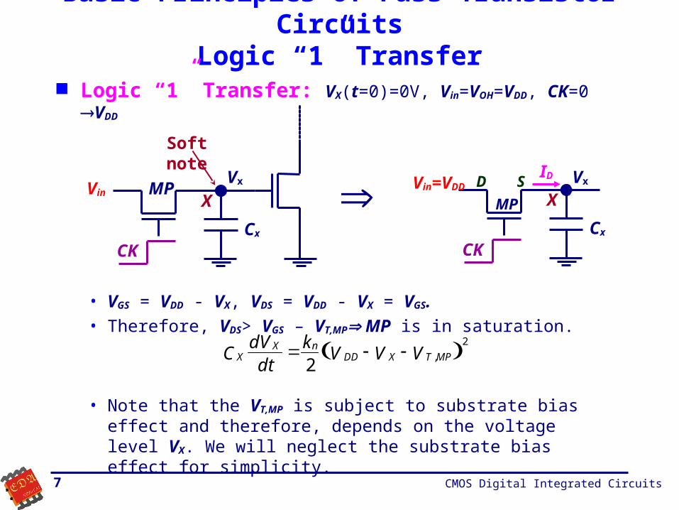
Basic Principles of Pass Transistor CircuitsLogic “1” Transfer
Logic “1” Transfer: VX(t=0)=0V, Vin=VOH=VDD, CK=0 VDD
• VGS = VDD - VX, VDS = VDD - VX = VGS.
• Therefore, VDS> VGS – VT,MP MP is in saturation.
• Note that the VT,MP is subject to substrate bias effect and therefore, depends on the voltage level VX. We will neglect the substrate bias effect for simplicity.
MP
CKCx
Vx
Soft note
X MP
CKCx
Vin=VDDVx
X
ID
Vin D S
VVVk
dtdV
C MPTXDDnX
X ,
2
2
CMOS Digital Integrated Circuits8
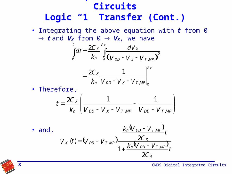
Basic Principles of Pass Transistor CircuitsLogic “1” Transfer (Cont.)
• Integrating the above equation with t from 0 t and VX from 0 VX, we have
• Therefore,
• and,
V
MPTXDDn
X
V
MPTXDD
X
n
Xt
X
X
VVVk
C
VVV
dV
k
Cdt
0,
0 ,
20
12
2
VVVVVk
CtMPTDDMPTXDDn
X
,,
112
t
CVVk
tC
VVk
VVtV
X
MPTDDn
X
MPTDDn
MPTDDX
21
2)(,
,
,

CMOS Digital Integrated Circuits9
Basic Principles of Pass Transistor CircuitsLogic “1” Transfer (Cont.)
• VX rises from 0V and approaches a limit value Vmax = VX(t)|t= = VDD-VT,MP, but it can not exceed this value, since the pass transistor will turn off at this point (VGS=VT,MP). Therefore, it transfers a “weak logic 1”.
• The actual Vmax by taking the body effect into account is,
• and tcharge = time to VX = 0.9Vmax,
• Body Effect: Reduce VX, and Increase tcharge
VVVVVk
C
MPTDDMPTmaxDDn
X
charget,,
1
9.0
12
22,0 FmaxFMPTDDmax VVVV
VX
VmaxVmax=VDD-VT,MP
t0
CMOS Digital Integrated Circuits10
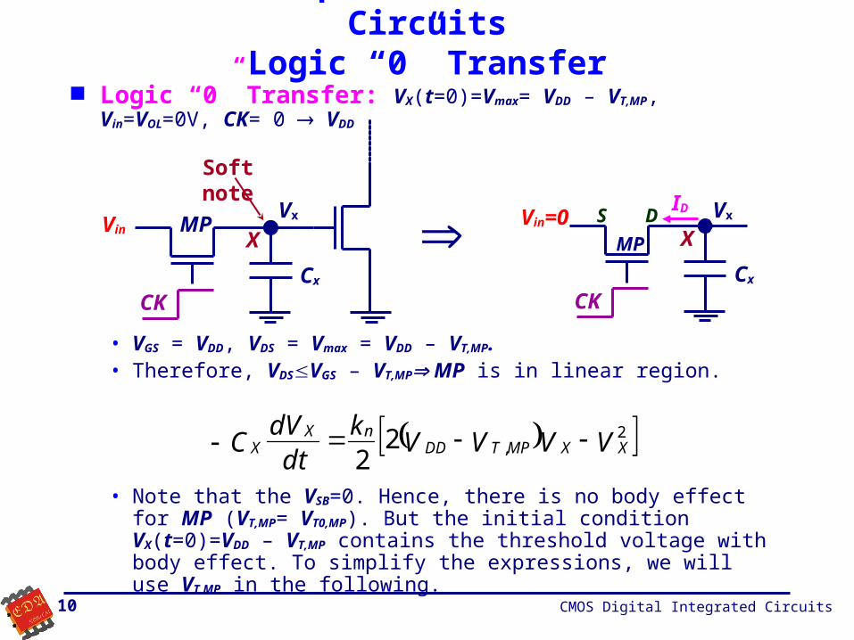
Basic Principles of Pass Transistor CircuitsLogic “0” Transfer
Logic “0” Transfer: VX(t=0)=Vmax= VDD – VT,MP, Vin=VOL=0V, CK= 0 VDD
• VGS = VDD, VDS = Vmax = VDD – VT,MP. • Therefore, VDSVGS – VT,MP MP is in linear region.
• Note that the VSB=0. Hence, there is no body effect for MP (VT,MP= VT0,MP). But the initial condition VX(t=0)=VDD – VT,MP contains the threshold voltage with body effect. To simplify the expressions, we will use VT,MP in the following.
MP
CKCx
Vx
Soft note
X MP
CKCx
Vin=0 Vx
X
ID
Vin DS
VVVVk
dtdV
C XXMPTDDnX
X2
,22

CMOS Digital Integrated Circuits11
Basic Principles of Pass Transistor Circuits Logic “0” Transfer (Cont.)
• Integrating the above equation with t from 0 t and VX from VT,MP VX, we have
• Therefore,
• and,
V
VVX
XMPTDD
MPTDDn
X
V
VV XXMPTDD
X
n
Xt
X
MPTDD
X
MPTDD
V
VVV
VVk
C
VVVV
dV
k
Cdt
,
,
,
,
2,0
2ln
22
V
VVV
VVk
CtX
XMPTDD
MPTDDn
X ,
,
2ln
e
VVtVCVVtk
MPTDDX
XMPTDDn
1
2)(
/
,
,

CMOS Digital Integrated Circuits12
Basic Principles of Pass Transistor Circuits Logic “0” Transfer (Cont.)
• VX drops from Vmax = VDD-VT,MP, to 0V. Hence, unlike the charge-up case, it transfers a “strong logic 0”.
fall = time of VX drops from 0.9Vmax to 0.1Vmax,
• where,
VVk
C2.74
VVk
C
tt
MPTDDn
X
MPTDDn
X
fall
,
,
%10%90
)22.1ln()19ln(
0.1
1.9
VVk
Ct
1.22VVk
C
VV0.9VV0.92
VVk
Ct
MPTDDn
X
MPTDDn
X
MPTDD
MPTDD
MPTDDn
X
ln
ln
ln
,%10
,
,
,
,%90
VX
VmaxVmax=VDD-VT,MP
t0

CMOS Digital Integrated Circuits13
Basic Principles of Pass Transistor Circuits Charge Storage and Charge Leakage
• At t = 0, CK=0, VX= Vmax, Vin =0. The charge stored in CX will gradually leak away, primarily due to the leakage currents associated with the pass transistor. The gate current of the inverter driver transistor is negligible.
n+ n+
VCK=0
Vin=0Ileakage VX
CX
Ireverse
Isubthreshold
p-type Si
MP
CK=0Cx
VxVin =0Ileakage Igate=0

CMOS Digital Integrated Circuits14
Basic Principles of Pass Transistor Circuits Charge Storage and Charge Leakage (Cont.)
• Isubthreshold is the subthreshold current for the pass transistor with CK=0.
• Ireverse is the reverse current for the source/drain pn junction at node X
• Cj (VX) : due to the reverse biased drain-substrate junction, a function of VX
• Cin: due to oxide-related parasitics, can be considered constants.
n+ n+
VCK=0Vin=0
Ileakage VX
CX
Ireverse
Isubthreshold
p-type Si
Cin
VxIleakage
Cj(VX)
Ileakage= Isubthreshold + Ireverse
Ireverse
Cin= Cgb + Cpoly + Cmetal
CX= Cin + Cj
Isubthreshold
Drain-substrate pn-junction
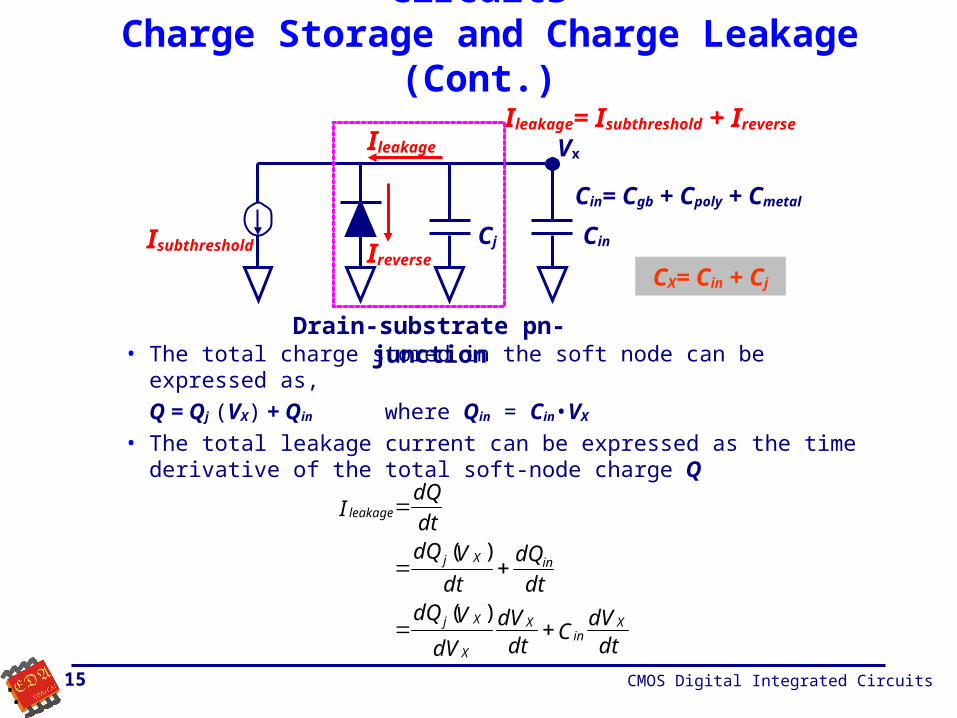
CMOS Digital Integrated Circuits15
Basic Principles of Pass Transistor Circuits Charge Storage and Charge Leakage (Cont.)
• The total charge stored in the soft node can be expressed as,
Q = Qj (VX) + Qin where Qin = Cin•VX
• The total leakage current can be expressed as the time derivative of the total soft-node charge Q
Cin
VxIleakage
Cj
Ileakage= Isubthreshold + Ireverse
Ireverse
Cin= Cgb + Cpoly + Cmetal
CX= Cin + Cj
Isubthreshold
Drain-substrate pn-junction
dtdV
Cdt
dV
dV
VdQdt
dQ
dt
VdQdt
dQI
Xin
X
X
Xj
inXj
leakage
)(
)(

CMOS Digital Integrated Circuits16
Basic Principles of Pass Transistor Circuits Charge Storage and Charge Leakage (Cont.)• Where
• Therefore,
• We have to solve the above differential equation to estimate the actual charge leakage time from the soft node.
n
NNq
kT
i
ASWDSW 20 ln
n
NNq
kT
i
AD
20 ln
SW
X
SWj
X
j
XjX
Xj
V
AC
V
AC
VCdV
VdQ
0
0
0
0
11
)()(
dtdV
CV
PC
V
ACI
Xin
SW
X
SWj
X
jleakage
0
0
0
0
11
CMOS Digital Integrated Circuits17
Basic Principles of Pass Transistor Circuits Charge Storage and Charge Leakage (Cont.)
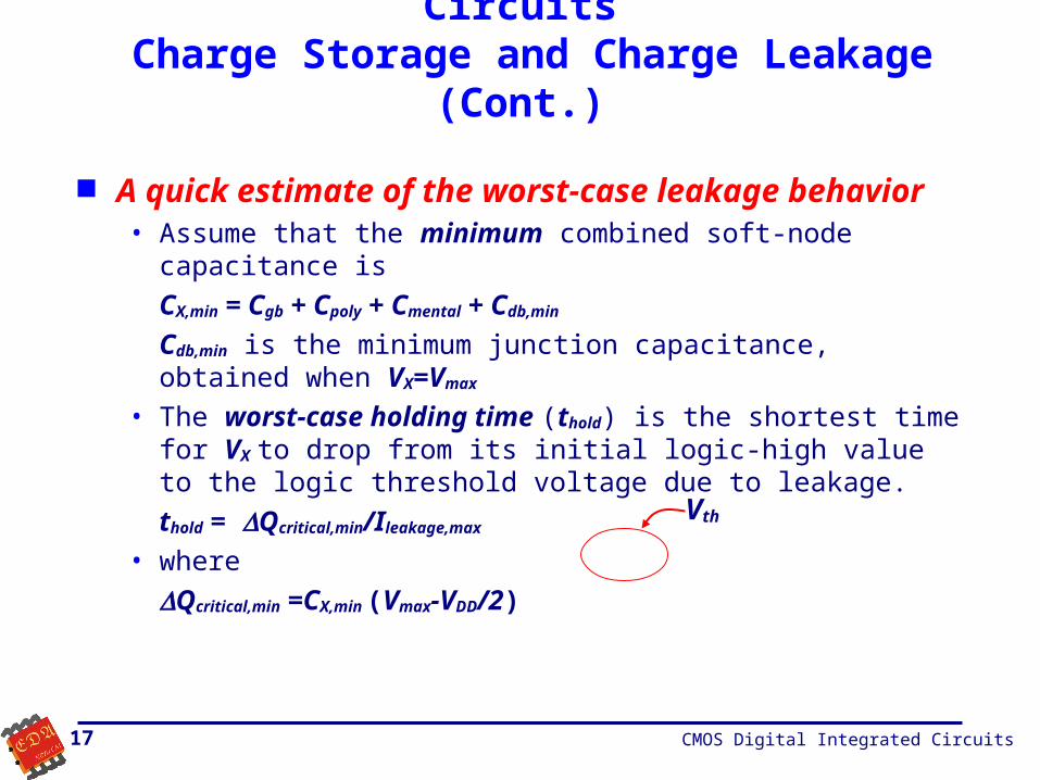
A quick estimate of the worst-case leakage behavior• Assume that the minimum combined soft-node capacitance is
CX,min = Cgb + Cpoly + Cmental + Cdb,min
Cdb,min is the minimum junction capacitance, obtained when VX=Vmax
• The worst-case holding time (thold) is the shortest time for VX to drop from its initial logic-high value to the logic threshold voltage due to leakage.
thold = Qcritical,min/Ileakage,max
• where
Qcritical,min =CX,min (Vmax-VDD/2)
Vth

CMOS Digital Integrated Circuits18
Basic Principles of Pass Transistor Circuits Charge Storage and Charge Leakage (Cont.)
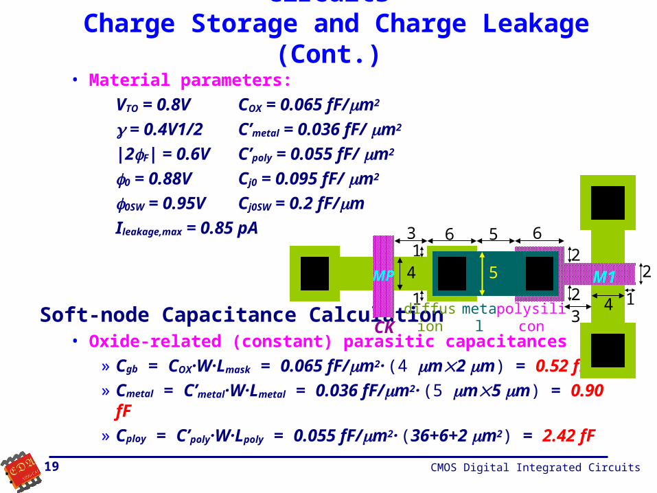
Example 9.2: Consider the soft-node structure shown below, which consists of the drain (or source, depending on current direction) terminal of the pass transistor, connected to the polysilicon gate of an nMOS driver transistor via a metal interconnect.
Question: is to estimate thold if VDD=5V and the soft-node is initially charged to Vmax.
MP
Cx
Vx
CK
M1
2
31
4
1 13
6 65
52
24
soft node
M1MP
diffusion metal polysiliconCK
CMOS Digital Integrated Circuits19
Basic Principles of Pass Transistor Circuits Charge Storage and Charge Leakage (Cont.)
• Material parameters:
VTO = 0.8V COX = 0.065 fF/m2
= 0.4V1/2 C’metal = 0.036 fF/ m2
|2F| = 0.6V C’poly = 0.055 fF/ m2
0 = 0.88V Cj0 = 0.095 fF/ m2
0SW = 0.95V Cj0SW = 0.2 fF/m
Ileakage,max = 0.85 pA
Soft-node Capacitance Calculation• Oxide-related (constant) parasitic capacitances
» Cgb = COX·W·Lmask = 0.065 fF/m2· (4 m2 m) = 0.52 fF
» Cmetal = C’metal·W·Lmetal = 0.036 fF/m2· (5 m5 m) = 0.90 fF
» Cploy = C’poly·W·Lpoly = 0.055 fF/m2· (36+6+2 m2) = 2.42 fF
2
31
4
1 13
6 65
52
24
M1MP
diffusion metal polysiliconCK

CMOS Digital Integrated Circuits20
Basic Principles of Pass Transistor Circuits Charge Storage and Charge Leakage (Cont.)
• Parasitic junction capacitance
By zero-bias unit capacitance values in the previous slide, we have
» Cbottom = Abottom·Cj0 = 0.095 fF/m2· (36 m2 + 12 m2 ) = 4.56 fF
» Csidewall = Cj0SW·Psidewall = 0.2 fF/m2· (30 m) = 6.00 fF
Therefore
» Cdb,max = Cbottom + Csidewall = 4.56 fF + 6.00 fF = 10.56 fF
The minimum drain junction capacitance is achieved as the junction is biased with Vmax. We need to find Vmax to determine Cdb,min
» Vmax = 5.0 - 8.0 - 0.4 ( 0.6+ Vmax - 0.6 )
Vmax = 3.68 V
Therefore,
fF
V
C
V
CC
SW
maxX
sidewall
maxX
bottommindb
71.4
95.068.3
1
0.6
88.068.3
1
56.4
110
,
0
,
,
CMOS Digital Integrated Circuits21
Basic Principles of Pass Transistor Circuits Charge Storage and Charge Leakage (Cont.)
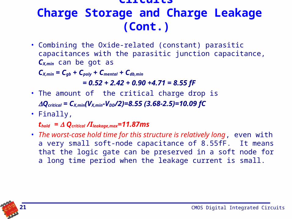
• Combining the Oxide-related (constant) parasitic capacitances with the parasitic junction capacitance, CX,min can be got as
CX,min = Cgb + Cpoly + Cmental + Cdb,min
= 0.52 + 2.42 + 0.90 +4.71 = 8.55 fF
• The amount of the critical charge drop is
Qcritical = CX,min(VX,min-VDD/2)=8.55 (3.68-2.5)=10.09 fC
• Finally,
thold = Qcritical /Ileakage,max=11.87ms
• The worst-case hold time for this structure is relatively long, even with a very small soft-node capacitance of 8.55fF. It means that the logic gate can be preserved in a soft node for a long time period when the leakage current is small.

CMOS Digital Integrated Circuits22
Voltage Bootstrapping
• The Voltage bootstrapping is a technique to overcome the threshold voltage drops of the output voltage levels in pass transistor gates or enhancement-load inverters and logic gates.
• Consider the following circuit with VXVDD M2 is in saturation. If Vin is low, the maximum output voltage is limited as
Vout(max) = VX – VT2(Vout)
M1Cout
Vx
Vin
M2
VDD
Vout

CMOS Digital Integrated Circuits23
Voltage Bootstrapping (Cont.)• To overcome the voltage drop, the voltage VX must be increased. This
can be achieved by adding a third transistor M3 into the circuit.
» CS and Cboot represent the capacitances which dynamically couple VX to the ground and to the output.
» The goal of the above circuit is to provide a high enough voltage VX to let Vout go to VDD instead of VDD-VT2(Vout).
• Initially, let Vin=H M1 and M2 are on, and Vout=L.
• Now Vin goes to L M1 turns off, and Vout starts to rise. This change will be coupled to VX through the bootstrap capacitor, Cboot.
M1 CoutVin
M2
VDD
Vout
Vx
M3
CbootCS
CMOS Digital Integrated Circuits24
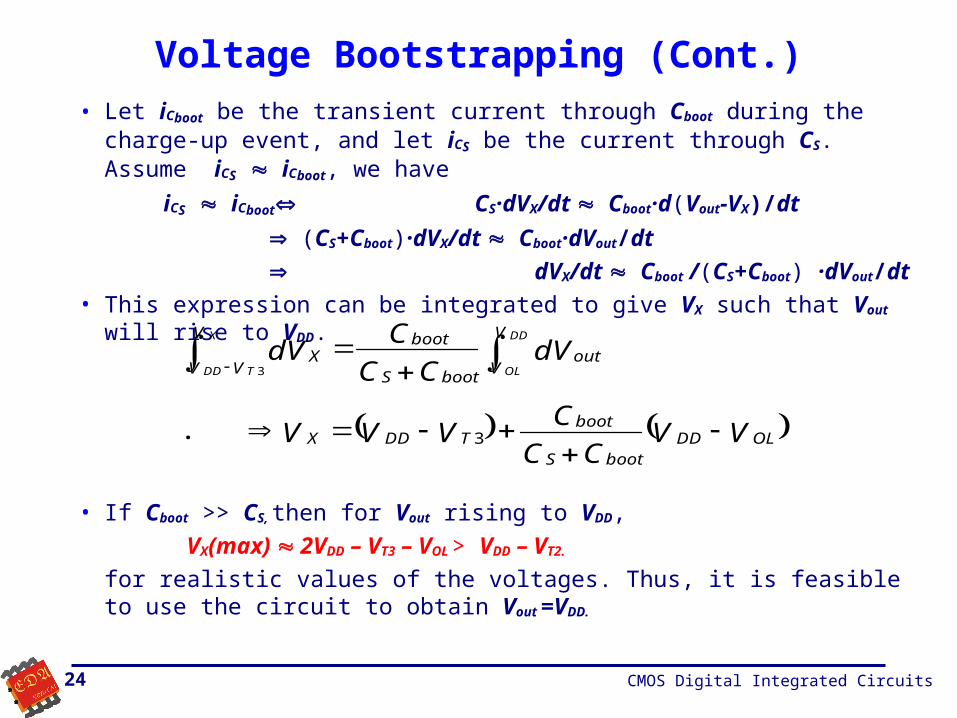
Voltage Bootstrapping (Cont.)
• Let iCboot be the transient current through Cboot during the charge-up event, and let iCS be the current through CS. Assume iCS iCboot, we have
iCS iCboot CS·dVX/dt Cboot·d(Vout-VX)/dt
(CS+Cboot)·dVX/dt Cboot·dVout/dt
dVX/dt Cboot /(CS+Cboot) ·dVout/dt
• This expression can be integrated to give VX such that Vout will rise to VDD.
• If Cboot >> CS, then for Vout rising to VDD,
VX(max) 2VDD – VT3 – VOL > VDD – VT2.
for realistic values of the voltages. Thus, it is feasible to use the circuit to obtain Vout =VDD.
VVCC
CVVV
dVCC
CdV
OLDDbootS
bootTDDX
V
Vout
bootS
bootV
VVX
DD
OL
X
TDD
3 .
3

CMOS Digital Integrated Circuits25
Voltage Bootstrapping (Cont.)
• To overcome the threshold voltage drop at Vout, the minimum VX is
VX(min) = VDD + VT2|Vout = VDD
= [VDD-VT3(VX)]+Cboot /(CS+Cboot) ·(VDD-VOL)
• Therefore, the required capacitance ratio Cboot /(CS+Cboot) is
• CS is the sum of the parasitic source-to-substrate capacitance of M3 and the gate-to-substrate capacitance of M2.
XDDout
XDDout
XDDout
VTVVTOLDD
VTVVT
S
boot
OLDD
VTVVT
bootS
boot
VVVV
VV
C
C
VV
VV
CC
C
32
32
32
.

CMOS Digital Integrated Circuits26
Voltage Bootstrapping (Cont.)• Cboot can be specifically constructed to control its value by using a
transistor with the source and drain connected together at Vout and the gate attached to VX. Since its drain and source tied together, it simply acts as an MOS capacitor between VX and Vout.
• See Kang and Leblebici at pp. 373 for a SPICE example.
M1Vin
M2
VDD
Vx
M3
Vout
Cboot
CMOS Digital Integrated Circuits27
Synchronous Dynamic Circuit Techniques –Dynamic Pass Transistor Circuits
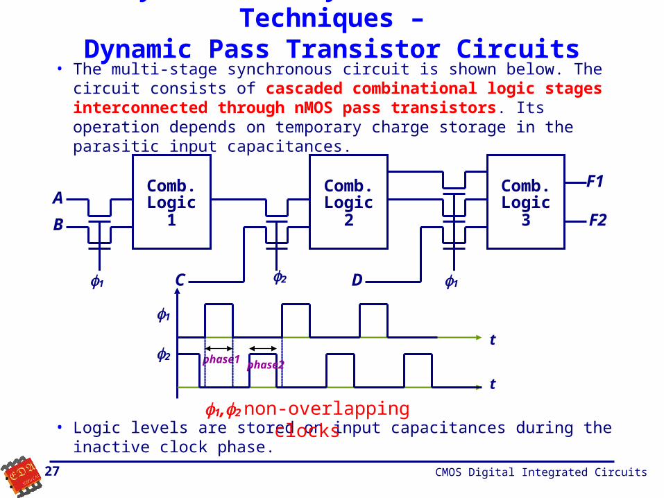
• The multi-stage synchronous circuit is shown below. The circuit consists of cascaded combinational logic stages interconnected through nMOS pass transistors. Its operation depends on temporary charge storage in the parasitic input capacitances.
• Logic levels are stored on input capacitances during the inactive clock phase.
A
B
112C D
F1
F2
Comb.Logic
1
Comb.Logic
2
Comb.Logic
3
1
phase1 phase2
t
t2
1,2 non-overlapping clocks
CMOS Digital Integrated Circuits28
Dynamic Pass Transistor CircuitsTwo-Phase Clock Dynamic Shift Register
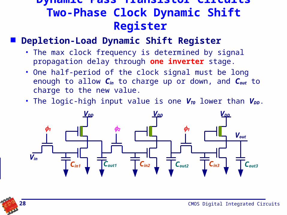
Depletion-Load Dynamic Shift Register• The max clock frequency is determined by signal propagation delay
through one inverter stage.
• One half-period of the clock signal must be long enough to allow Cin to charge up or down, and Cout to charge to the new value.
• The logic-high input value is one VT0 lower than VDD.
VDD
1 2 1
Vin
Vout
Cin1 Cin2 Cin3Cout1 Cout2
VDD VDD
Cout3
CMOS Digital Integrated Circuits29
Dynamic Pass Transistor Circuits Enhancement-Load Dynamic Shift Register
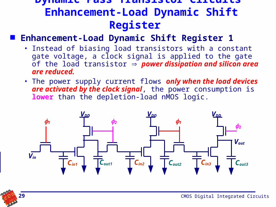
Enhancement-Load Dynamic Shift Register 1• Instead of biasing load transistors with a constant gate voltage, a clock
signal is applied to the gate of the load transistor power dissipation and silicon area are reduced.
• The power supply current flows only when the load devices are activated by the clock signal, the power consumption is lower than the depletion-load nMOS logic.
VDD
1 2 1
Vin
Vout
Cin1 Cin2 Cin3Cout1 Cout2
VDD VDD
Cout3
2
CMOS Digital Integrated Circuits30
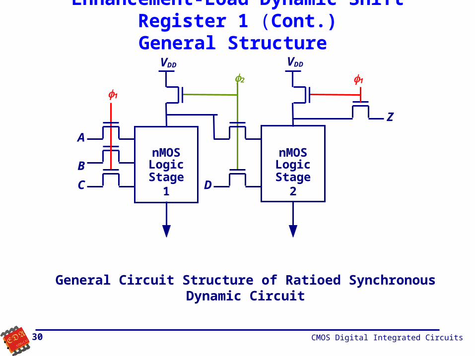
Enhancement-Load Dynamic Shift Register 1 (Cont.)General Structure
B
C
1
VDD
nMOSLogic
Stage 1
nMOSLogic
Stage 2
A
D
VDD
2 1
Z
General Circuit Structure of Ratioed Synchronous Dynamic Circuit

CMOS Digital Integrated Circuits31
Enhancement-Load Dynamic Shift Register 1 (Cont.) VDD
1
2 1
Vin
Vout3
Cin1 Cin2 Cin3Cout1 Cout2
VDD VDD
Cout3
2Vout1 Vout2
Vout2VOL
VDD
1
2 1
Vin
Cin1 Cin2 Cin3Cout1 Cout2
VDD VDD
Cout3
2
1=H
2=H
Vout1 Vout2 Vout3
Vout1VOL Vout3VOL
• VOL → kdriver/kload Ratioed Dynamic Logic.
• Cout1, Cin2 & Cout2, Cin3 interact Charge Sharing
CMOS Digital Integrated Circuits32
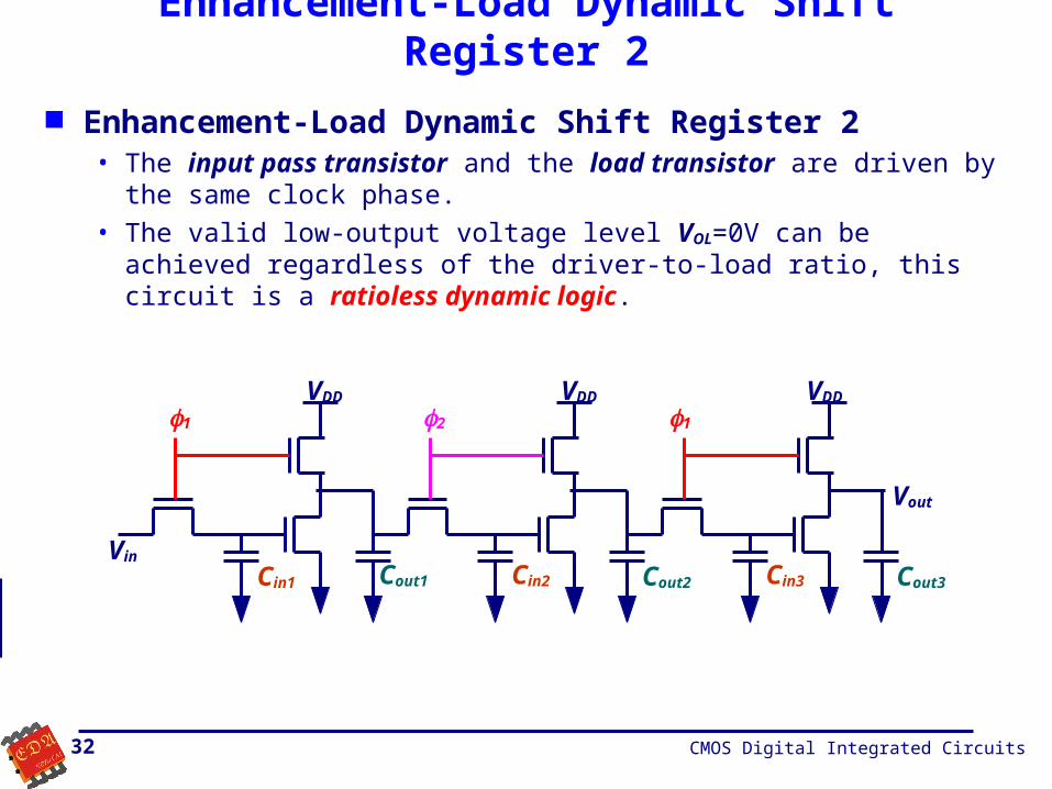
Enhancement-Load Dynamic Shift Register 2
Enhancement-Load Dynamic Shift Register 2• The input pass transistor and the load transistor are driven by the same
clock phase.
• The valid low-output voltage level VOL=0V can be achieved regardless of the driver-to-load ratio, this circuit is a ratioless dynamic logic.
VDD
1 2 1
Vin
Vout
Cin1 Cin2 Cin3Cout1 Cout2
VDD VDD
Cout3
CMOS Digital Integrated Circuits33
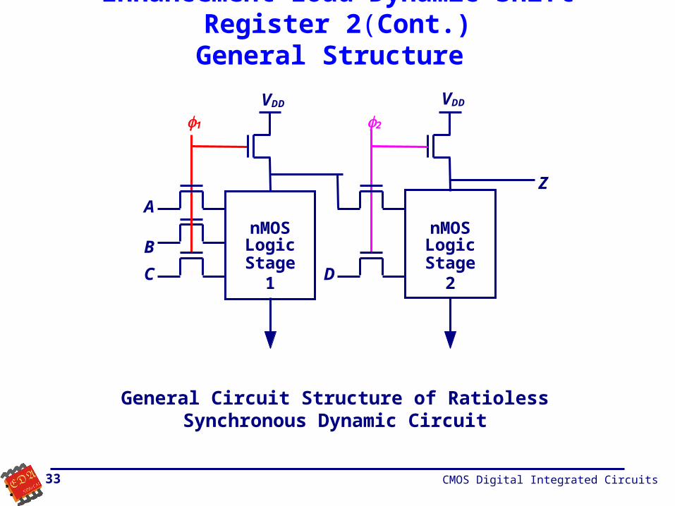
Enhancement-Load Dynamic Shift Register 2(Cont.)General Structure
General Circuit Structure of Ratioless Synchronous Dynamic Circuit
B
C
1
VDD
nMOSLogic
Stage 1
nMOSLogic
Stage 2
A
D
VDD
2
Z

CMOS Digital Integrated Circuits34
Enhancement-Load Dynamic Shift Register 2 (Cont.)
• VOL → 0V Ratioless Dynamic Logic.
• Cini << Couti-1 for i=2,3 Minimum Charge Sharing
VDD
12 1
Vin
Vout3
Cin1 Cin2 Cin3Cout1 Cout2
VDD VDD
Cout3
Vout1 Vout2
Vout2 0VVDD
1 2 1
Vin
Cin1 Cin2 Cin3Cout1 Cout2
VDD VDD
Cout3
1=H
2=H
Vout1 Vout2 Vout3
Vout10V Vout30V
Vout1VOL Vout3VOL
Vout2VOL

CMOS Digital Integrated Circuits35
Enhancement-Load Dynamic Shift Register 2 (Cont.)Charge Sharing
2 = 0: Qout1 = Cout1Vb and Qin2 = Cin2Va
2 = 1: Qtotal = Cout1Vb + Cin2Va and Ctotal = Cout1 + Cin2
The resulting voltage across Ctotal is
VR = Qtotal / Ctotal = (Cout1Vb + Cin2Va )/ (Cout1 + Cin2)
• If Vb = VDD and Va << Vb VR Cout1VDD /(Cout1 + Cin2)
VR VDD if Cin2 << Cout1
2
Cin2Cout1
Vb Va
Charge Sharing
CMOS Digital Integrated Circuits36
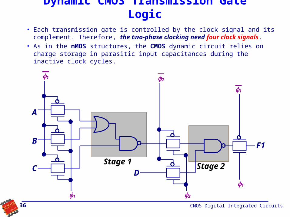
Dynamic CMOS Transmission Gate Logic• Each transmission gate is controlled by the clock signal and its
complement. Therefore, the two-phase clocking need four clock signals.• As in the nMOS structures, the CMOS dynamic circuit relies on charge
storage in parasitic input capacitances during the inactive clock cycles.
D
1 2
A
B
CStage 1
Stage 2
1
1
1
2
F1
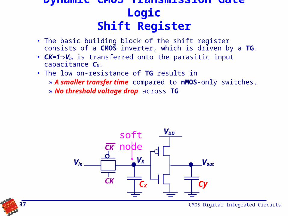
CMOS Digital Integrated Circuits37
Dynamic CMOS Transmission Gate LogicShift Register
• The basic building block of the shift register consists of a CMOS inverter, which is driven by a TG.
• CK=1Vin is transferred onto the parasitic input capacitance CX.• The low on-resistance of TG results in
» A smaller transfer time compared to nMOS-only switches.» No threshold voltage drop across TG
CK
VDD
VoutVX
CX CyCK
Vin
soft node
CMOS Digital Integrated Circuits38
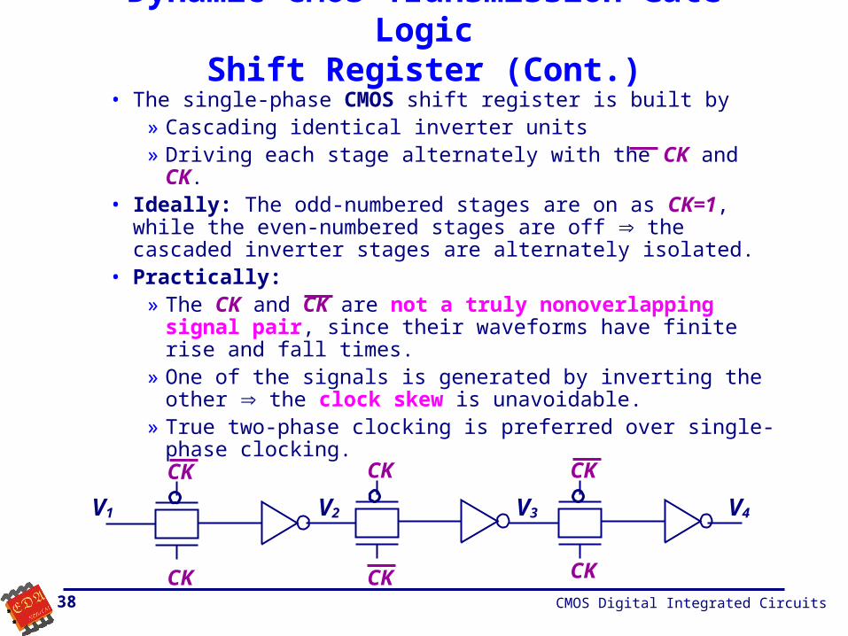
Dynamic CMOS Transmission Gate LogicShift Register (Cont.)
• The single-phase CMOS shift register is built by» Cascading identical inverter units» Driving each stage alternately with the CK and CK.
• Ideally: The odd-numbered stages are on as CK=1, while the even-numbered stages are off the cascaded inverter stages are alternately isolated.
• Practically:» The CK and CK are not a truly nonoverlapping signal pair,
since their waveforms have finite rise and fall times.» One of the signals is generated by inverting the other the
clock skew is unavoidable.» True two-phase clocking is preferred over single-phase
clocking.CK
CK
V1
CK
CK
CK
CK
V2 V3 V4
CMOS Digital Integrated Circuits39
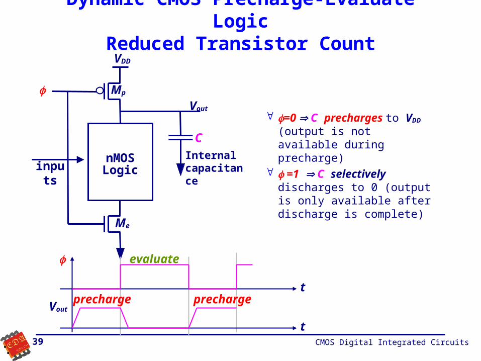
Dynamic CMOS Precharge-Evaluate LogicReduced Transistor Count
=0 C precharges to VDD (output is not available during precharge)
=1 C selectively discharges to 0 (output is only available after discharge is complete)
VDD
nMOSLogicinputs
C
Vout
Me
Mp
Internal capacitance
t
t
Voutprecharge precharge
evaluate
CMOS Digital Integrated Circuits40
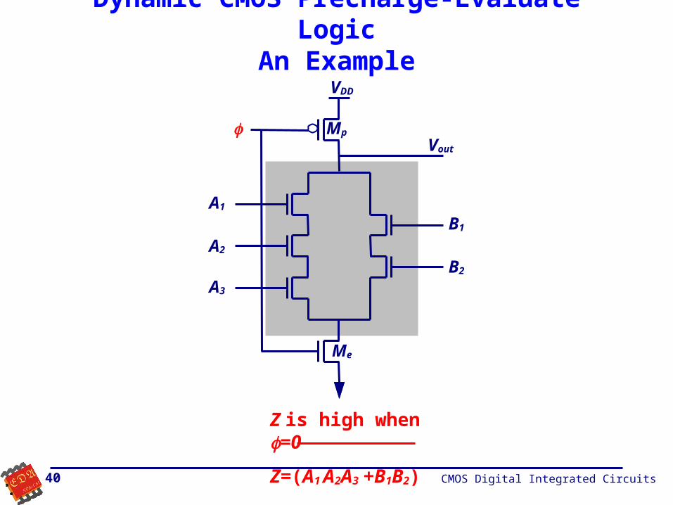
Dynamic CMOS Precharge-Evaluate LogicAn Example
VDD
Vout
Me
Mp
A1
A2
A3
B1
B2
Z is high when =0
Z=(A1 A2A3 +B1B2)

CMOS Digital Integrated Circuits41
Dynamic CMOS Precharge-Evaluate LogicAdvantages/Disadvantages
Advantages• Need only N+2 transistors to implement a N-input gate.• Low static power dissipation• No DC current paths to place constraints on device sizing• Input capacitance is same as pseudo nMOS gate.• Pull-up time is improved by active switch to VDD.
Disadvantages• The available time of output is less than 50 % of the time.• Pull-down time is degraded due to series active switch to 0.• Logic output value can be degraded due to charge sharing with other gate
capacitances connected to the output.• Minimum clock rate determined by leakage on C.• Maximum clock rate determined by circuit delays.• Input can only change during the precharge phase. Inputs must be stable
during evaluation; otherwise an incorrect value on an input could erroneously discharge the output node. (single phase P-E logic gates can not be cascaded)
• Outputs must be stored during precharge, if they are required during the next evaluate phase.
CMOS Digital Integrated Circuits42
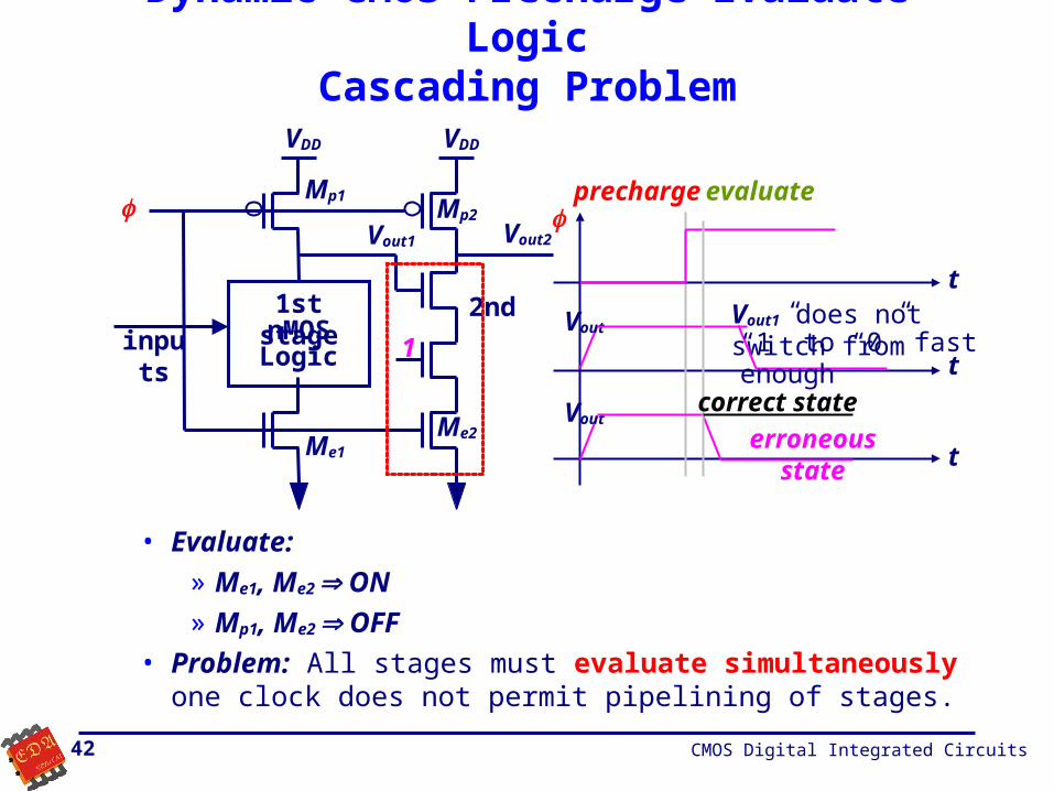
Dynamic CMOS Precharge-Evaluate LogicCascading Problem
• Evaluate:
» Me1, Me2 ON
» Mp1, Me2 OFF
• Problem: All stages must evaluate simultaneously one clock does not permit pipelining of stages.
VDD
nMOSLogic
Vout1
1st stage
1
Vout2
VDD
2nd Vout1 does not switch fromt
t
Vout
t
Voutcorrect state
erroneous state
precharge evaluate
“1” to “0” fast enoughinputs
Me1
Me2
Mp1Mp2
CMOS Digital Integrated Circuits43
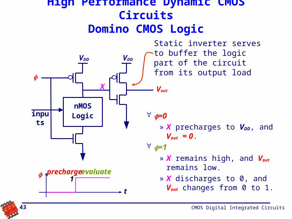
High Performance Dynamic CMOS CircuitsDomino CMOS Logic
VDD
nMOSLogic
Vout
VDD
inputs
X
precharge evaluate1
t
Static inverter serves to buffer the logic part of the circuit from its output load
=0
» X precharges to VDD, and Vout = 0. =1
» X remains high, and Vout remains low.
» X discharges to 0, and Vout changes from 0 to 1.

CMOS Digital Integrated Circuits44
Domino CMOS Logic
VDD
nMOSLogicinputs
VDD
nMOSLogic
X1
VDD
nMOSLogic
X2 X3
t
t
X1
t
precharge
evaluate
t
X2
X3
evaluate
teval
Max number gates limited: total propagation delay < teval

CMOS Digital Integrated Circuits45
Domino CMOS Logic (Cont.)
• The problem in cascading conventional dynamic CMOS occurs when one or more inputs make a 1 to 0 transition during evaluation.
• Domino circuits can fix the above problem
» During the evaluation, each buffer output can make at most one transition (from 0 to 1), and thus each input of all subsequent logic stages can also make at most one (0 to 1) transition.
X3
VDD
nMOSLogicinputs
VDD
nMOSLogic
X1
VDD
nMOSLogic
X2
CMOS Digital Integrated Circuits46
Domino CMOS Logic The Limitations
• The static CMOS and domino gates can be used together, see Fig. 9.31. in Kang and Leblebici. The limitation: the number of inverting static logic stages in cascade must be even, to let the inputs of next domino stage can have only 0 to 1 transitions during the evaluation.
• Can implement only non-inverting logic • Due to precharge use, can suffer from charge sharing during the
evaluation which may cause erroneous outputs.» The problem will be described in the next slide, and several
solutions will be presented later.
CMOS Digital Integrated Circuits47
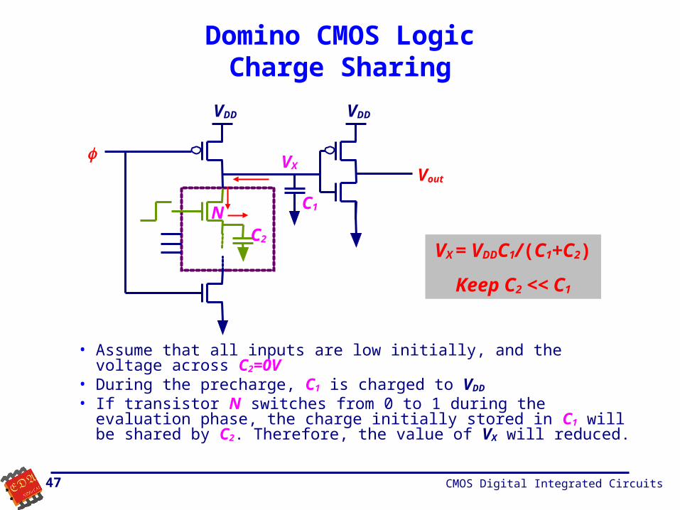
Domino CMOS LogicCharge Sharing
• Assume that all inputs are low initially, and the voltage across C2=0V• During the precharge, C1 is charged to VDD
• If transistor N switches from 0 to 1 during the evaluation phase, the charge initially stored in C1 will be shared by C2. Therefore, the value of VX will reduced.
VDD
Vout
VDD
VX
C1
C2
VX = VDDC1/(C1+C2)
Keep C2 << C1
N

CMOS Digital Integrated Circuits48
Domino CMOS LogicReduce Charge Sharing Degradation of VX
VDD
nMOSLogicinputs
VoutVX
Push VX to VDD unless there is a strong pull-down path between Vout and ground
weak pull-up pMOS
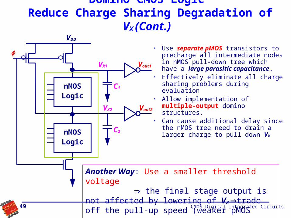
CMOS Digital Integrated Circuits49
Domino CMOS Logic Reduce Charge Sharing Degradation of VX (Cont.)
• Use separate pMOS transistors to precharge all intermediate nodes in nMOS pull-down tree which have a large parasitic capacitance.
• Effectively eliminate all charge sharing problems during evaluation
• Allow implementation of multiple-output domino structures.
• Can cause additional delay since the nMOS tree need to drain a larger charge to pull down VX
VDD
nMOSLogic
Vout1
VX2
VX1
nMOSLogic
Vout2
C1
C2
Another Way: Use a smaller threshold voltage the final stage output is not affected by lowering of VX trade off the pull-up speed (weaker
pMOS transistor)

CMOS Digital Integrated Circuits50
Domino CMOS Logic An Example of Using Separate pMOS Transistor
VDD
VDD
Vout
VDD
VX1
C1
C2
VA
VB
VX2
• Let C1 = C2 = 0.05pF. VX1 = 0, and VX2 = 0 at t=0
• Without this extra pMOS transistor
» Precharge: VX1 ≠VX2
» Evaluation: VX1 = VDDC1/(C1+C2) = VDD/2
• With this extra pMOS transistor
» Presharge: VX1 = VX2
» Evaluation: VX1 = VDD
• See pp.392~393 for the HSPICE simulation result
• Note that there is a speed penalty for adding this extra pMOS precharge transistor.

CMOS Digital Integrated Circuits51
Domino CMOS LogicAn Example of Multiple-Output Domino Circuits
• C1=G1+P1C0
• C2=G2+P2G1+P2P1C0
• C3=G3+P3G2+P3P2G1+P3P2P1C0
• C4=G4+P4G3+P4P3G2+P4P3P2G1+P4P3P2P1C0
P1
C0
P2
P3
P4
G2
G3
G1
G4
C4
C3
C2
C1
VDD
Gi = Ai · Bi
Pi = Ai Bi
Reduce transistor count

CMOS Digital Integrated Circuits52
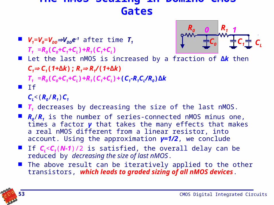
FET Scaling in Domino CMOS Gates The transient performance can be improved by adjusting
the nMOS transistor sizes in the pull-down path to reduce the discharge time.
VDD
Vout
Me
Mp
A
B
C
D
CL
CLC1C0
R0 R10 1
ABCD
CMOS Digital Integrated Circuits53
The nMOS Scaling in Domino CMOS Gates
V1=V0=VDDVDDe-1 after time T1
T1 =R0(C0+C1+CL)+R1(C1+CL) Let the last nMOS is increased by a fraction of ∆k then
C1 C1(1+∆k); R1 R1/(1+∆k)
T1 =R0(C0+C1+CL)+R1(C1+CL)+(C1-R1CL/R0)∆k If
CL<(R0/R1)C1
T1 decreases by decreasing the size of the last nMOS. R0/R1 is the number of series-connected nMOS minus one, times a factor
γ that takes the many effects that makes a real nMOS different from a linear resistor, into account. Using the approximation γ=1/2, we conclude
If CL<C1(N-1)/2 is satisfied, the overall delay can be reduced by decreasing the size of last nMOS.
The above result can be iteratively applied to the other transistors, which leads to graded sizing of all nMOS devices.
CLC1C0
R0 R10 1

CMOS Digital Integrated Circuits54
NORA CMOS Logic (NP-Domino Logic)
• Advantages» An Inverter is not required at the output of stages» Allow pipelined system architecture
• Disadvantages: Also suffer from charge sharing and leakage
VDD VDD VDD
nMOSLogic
pMOSLogic
nMOSLogic
to nMOS stage to pMOS stage
nMOS stageprecharge
pMOS stagepre-discharge
all stagesevaluate
nMOS stageprecharge
pMOS stagepre-discharge
all stagesevaluate
CMOS Digital Integrated Circuits55
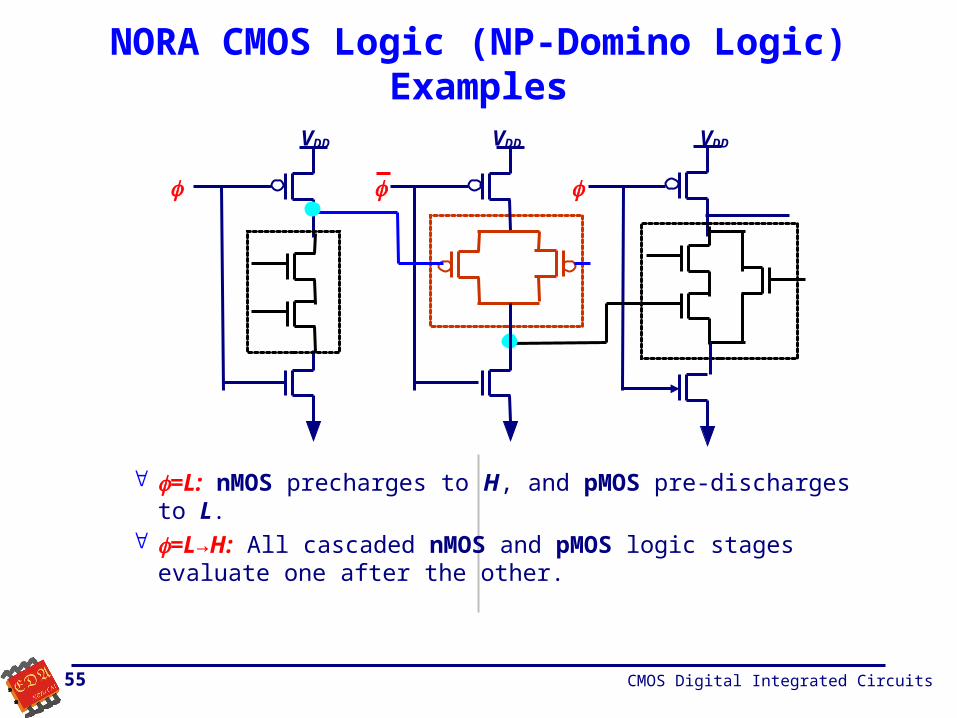
NORA CMOS Logic (NP-Domino Logic)Examples
VDD VDD VDD
=L: nMOS precharges to H, and pMOS pre-discharges to L. =L→H: All cascaded nMOS and pMOS logic stages evaluate
one after the other.

CMOS Digital Integrated Circuits56
NORA CMOS Logic (NP-Domino Logic)Examples (Cont.)
• Pipelined System Architecture: See Fig. 9.39 – Use of CMOS2 latches (three state latches storing on logic inputs.)
• Zipper Logic: See Fig. 9.40 – Identical to NORA except for weird clock signals that keep precharge devices weakly on to handle charge leakage and charge sharing
CMOS Digital Integrated Circuits57
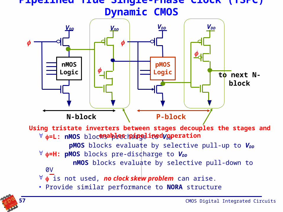
Pipelined True Single-Phase Clock (TSPC) Dynamic CMOS
=L: nMOS blocks precharge to VDD
pMOS blocks evaluate by selective pull-up to VDD
=H: pMOS blocks pre-discharge to VDD
nMOS blocks evaluate by selective pull-down to 0V is not used, no clock skew problem can arise.• Provide similar performance to NORA structure
Using tristate inverters between stages decouples the stages and enables pipelined operation
VDD VDD
nMOSLogic
pMOSLogic
VDD
VDD
N-block P-block
to next N-block
CMOS Digital Integrated Circuits58
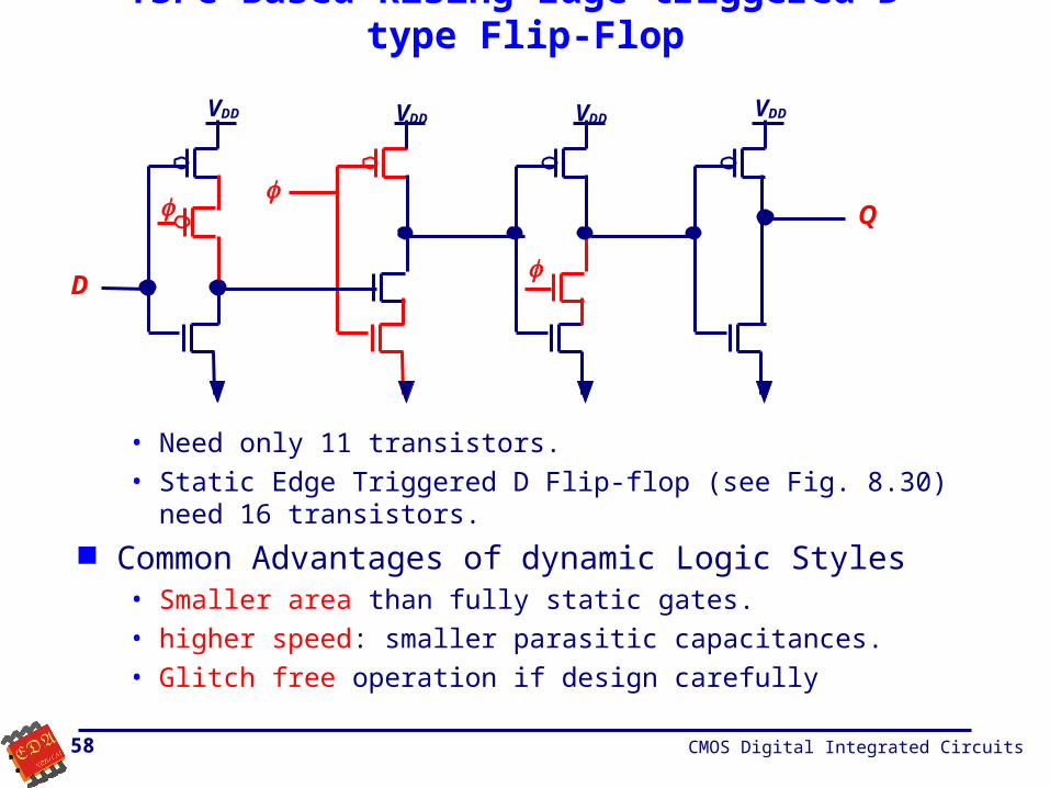
TSPC-Based Rising Edge-triggered D-type Flip-Flop
• Need only 11 transistors.
• Static Edge Triggered D Flip-flop (see Fig. 8.30) need 16 transistors.
Common Advantages of dynamic Logic Styles• Smaller area than fully static gates.
• higher speed: smaller parasitic capacitances.
• Glitch free operation if design carefully
VDD
VDD
VDD
Q
VDD
D
CMOS Digital Integrated Circuits59
Summary
• Full complementary static logic is best option in the majority of CMOS circuits.
» Noise-immunity is not sensitive to kn/kp
» Does not involve precharge of nodes
» Dissipate no DC power
» Layout can be automated
» Large fan-in gates lead to complex circuit structures (2N transistors)
» Larger parasitics
» Slower and higher dynamic power dissipation than alternatives
» No clock

CMOS Digital Integrated Circuits60
Summary (Cont.)
• Pseudo-nMOS static logic finds widest utility in large fan-in NOR gates.
» Require only N+1 transistors for N fan-in
» Smaller parasitics
» Faster and lower dynamic power dissipation than full CMOS
» Noise immunity sensitive to kn/kp
» Dissipate DC power when pulled down
» Not well suited for automated layout
» No clock

CMOS Digital Integrated Circuits61
Summary (Cont.)
• CMOS domino logic should be used for low-power, high speed applications
» Require only N+k transistors for N fan-in, size advantages of pseudo-nMOS.
» Dissipate no DC power» Noise immunity is not sensitive to kn/kp
» Use of clocks enables synchronous operation» Rely on storage on soft node» Require exhaustive simulation at all the process corners to
insure proper operation» Some of the speed advantage over static gates is diminished by
the required per-charge (pre-discharge) time.