CMOS 65nm Process Monitor - Home - Walter Scott, Jr...
25
CMOS 65nm Process Monitor 1 Final Report CMOS 65nm Process Monitor Final Report Spring Semester 2009 Prepared to partially fulfill the requirements for ECE402 Department of Electrical and Computer Engineering Colorado State University Fort Collins, CO 80523 By: Sheming Chen Phillip Misek Ryan Hoppal Report Approved: ___________________________________ Project Advisor ___________________________________ Senior Design Coordinator
Transcript of CMOS 65nm Process Monitor - Home - Walter Scott, Jr...

CMOS 65nm Process Monitor 1 Final Report
CMOS 65nm Process Monitor
Final Report Spring Semester 2009
Prepared to partially fulfill the requirements for ECE402
Department of Electrical and Computer Engineering
Colorado State University Fort Collins, CO 80523
By: Sheming Chen Phillip Misek Ryan Hoppal
Report Approved: ___________________________________ Project Advisor ___________________________________ Senior Design Coordinator

CMOS 65nm Process Monitor 2 Final Report
Abstract: Process variation is an important issue that process engineers and circuit designers must allow for when designing in today’s nanometer CMOS process technologies. Variations in gate lengths, widths, random doping fluctuations and threshold voltage affect the behavior and relative matching of transistors. In order to design more effectively, the circuit designer needs to know where in the process certain parameters are. Historically, most process characterization has been done on the wafer level, not on individual dies. These process monitors have typically been very large and complex, often taking up an entire die themselves. These monitors are usually implemented to look at the elusive underlying parameters, not at the intermediated results used for on-the-fly circuit adjustments. Several of these monitors would be spread about on a wafer and used for binning or characterization. As process technologies began to move past the 180nm mark, there was an increased interest in digital correction of individual dies. This has led to process monitors of various sorts being implemented on individual dies to provide more optimized performance. Most of the previous work done in this area relies on two basic principles, PTAT currents and frequency domain analysis. While PTAT currents have been used for a long time in reference circuits, they are beginning to run into some unique constraints in deep sub-micron geometries. Also, many of the circuits used to generate PTAT currents are physically unable to operate at the low supply voltages present in modern high performance circuits. Frequency domain analysis is becoming increasingly popular due to the very high switching speeds present in advanced digital circuits. The goal of this project is to create a modular process monitor that can easily be fit onto a pre existing die. This report describes the subsequent design of a CMOS process monitor that will measure inverter delay and polyresistance variation. The main test structure uses multiple ring oscillators with different loads. High speed counters and adders are used to process the signals, and the final result is output as an 8 bit word. The test circuit also has front-end digital control logic that enables the user to select which parameters are tested, and how the data is processed. This control logic also allows the test structures to be turned off to save power. Included in this paper is the final layout of many individual circuit pieces as well as extracted circuit simulation results for proof of design. Since our test circuits follow a modular design and functionality, future work may be done to analyze other process parameters. A module measuring the threshold voltage is probably the next logical expansion.

CMOS 65nm Process Monitor 3 Final Report
Table of Contents
Title .............................................................................................................................................................. 1
Abstract ......................................................................................................................................................... 2
Table of Contents ......................................................................................................................................... 3
List of Figures and Tables .............................................................................................................................. 4
I. Introduction ..................................................................................................................................... 5
II. Tools and Libraries .......................................................................................................................... 7
III. Overall Design ................................................................................................................................. 9
a. Digital Framework ............................................................................................................. 10
b. Inverter Delay Module ...................................................................................................... 10
i. Background/Theory/Design ................................................................................ 10
ii. Schematic Design ................................................................................................. 11
iii. Simulation ............................................................................................................ 11
iv. Layout .................................................................................................................. 12
v. Final Simulation ................................................................................................... 12
vi. Usage of Circuit .................................................................................................... 13
c. Counter ............................................................................................................................. 13
d. Poly-Resistance Module .................................................................................................... 15
i. Theory/Design ...................................................................................................... 15
ii. Schematic Design ................................................................................................. 16
iii. Simulation ............................................................................................................ 17
iv. Layout .................................................................................................................. 18
v. Final Simulation ................................................................................................... 19
vi. Usage of Circuit .................................................................................................... 20
IV. Conclusions and Future Work ........................................................................................................ 21
V. Acknowledgements........................................................................................................................ 23
VI. Bibliography ................................................................................................................................... 23
Appendix #1: Abbreviations ........................................................................................................................ 24
Appendix #2: Budget ................................................................................................................................... 25
CMOS 65nm Process Monitor 4 Final Report
List of Figures:
Figure 1 Wafer yield map 5 Figure 2 Normalized wafer to wafer and die to die variations for the 65nm process 6 Figure 3 Design flow diagram 8 Figure 4 Hierarchical model of our process monitor 9 Figure 5 Overall block diagram 10 Figure 6 Basic ring oscillator structure 11 Figure 7 Initial ring oscillator layout 12 Figure 8 Final ring oscillator layout 12 Figure 9 Final ring oscillator extracted simulation 13 Figure 10 3-bit counter block implemented with D-FlipFlops, NAND, and INV logic 14 Figure 11 9-bit counter formed by cascading three smaller cells 14 Figure 12 Final counter layout 14 Figure 13 Loaded ring oscillator schematic 15 Figure 14 Polyresistance module running in parallel with inverter delay module 16 Figure 15 Frequency vs. Resistance plot for a 100 stage resistively loaded RO 17 Figure 16 Resistance vs. Frequency for difference transistors 18 Figure 17 Final loaded ring oscillator layout 19 Figure 18 Extracted simulation of polyresistance module 20 Figure 19 Year long time allocation 21 Figure 20 Final layout for circuit 22 Figure 21 Budget 25

CMOS 65nm Process Monitor 5 Final Report
I. Introduction:
Process variation invariably occurs in the fabrication of CMOS devices. The process parameters of a CMOS technology can vary lot-to-lot, wafer-to-wafer, and die-to-die. Even though there have been advancements in lithographic technology to put down more identically-drawn devices, random distributions of these devices still occur because of variations in doping densities, oxide thicknesses, and diffusion depths, just to name a few. These variations result from non-uniform conditions during the deposition and diffusion of the impurities, greatly affecting the behavior of the devices. This variation is of critical importance in both analog and digital circuit designs, especially in circuits that rely on relative device matching. The significance and complexity of process variation becomes even more prominent with transistor size scaling. As we get in deep-sub-micron CMOS processes, circuit designers must increasingly account for process variations in their designs. In the 65nm process, process variations are a huge challenge. Devices are placed so close together that layout dependent stress variations (which are not normally encountered in larger device geometries), become an important factor. This is illustrated in the wafer yield map in Figure 1. This map shows variations in frequency parameters from die to die.
Figure 1: Wafer Yield Map

CMOS 65nm Process Monitor 6 Final Report
Since a circuit design must meet its specifications under all possible conditions, we need to know where in the process each particular wafer or particular die is. For example, if the die is fast or slow? Process monitoring circuits are used to characterize the performance of each die or wafer. The goal of our project is to design a monitor that will tell us the location in the process of gate delay and polysilicon resistance. We will be using ring oscillator test structures since they provide a statistical normalization across many devices. We organized our test structures into a modular design, so that this process monitor can support future expansion. First, we will discuss our findings from our first-year research into process variations and process monitors. We will then go into detail describing our circuit design, starting with the circuit theory and concepts, analysis in the frequency domain, our circuit schematics, and SPICE simulations for each of our process monitor modules. Then we will discuss the design of our digital circuits that control the circuit modules and the outputs. Finally we will go over the results from our extracted circuit and step through the process of using these results in order to tell the designer where in the process the circuit is.
Figure 2: Normalized Wafer to Wafer and Die to Die Variations for a 65nm Process
Note the skew targets denoting the different process corners.

CMOS 65nm Process Monitor 7 Final Report
II. Tools and Libraries: There are a few industry standard integrated-circuit design tools on the market. The two most widely used are Mentor Graphics’ Design Architect-IC and Cadence’s Custom IC Design Suites. These software packages provide an integrated solution to designing analog and digital circuits. At the beginning of the fall semester, we had hoped to have the Cadence toolset for us to use at CSU. In the end, due to financial considerations and contract negotiation delays, we were not successful in obtaining access to the Cadence tool set at CSU. Our design team spent many hours contacting the CSU professors and our project advisors to find out about the progress of the tools. In early October, our team decided we couldn’t waste any more time waiting for Cadence tools at CSU; and we decided to go ahead and start our designs using Mentor Graphics Design Architect. We spent a few weeks learning DA-IC and Mentor Graphics’ circuit layout tool. Charles Thangaraj, a PhD student in the VLSI System Design Lab, gave us some great tutorials and helped us to get started in the Mentor tool system. Charles led us through most of the design process, from schematic capture and layout to extracting parasitic elements and performing Design Rule Checks (DRC). We wanted to start our process monitor design in the Mentor tools, but we quickly ran into a few issues. Using the Mentor tools at CSU, we found that undergraduate students only had access to the older version of Mentor Graphics. This was a problem because the transistor libraries used in the VLSI lab were not correctly mapped to the older version of Mentor Graphics. This prevented us from laying out any schematics, let alone performing circuit simulations. Since our project emphasis was to design a process monitor for a 65nm process technology, we needed a good set of libraries that included BSIMv4 SPICE or HSPICE models to run our simulations. We needed accurate estimates of the gate delay times of our transistors in order to determine the optimal number of stages of our ring oscillator, and we could not predict these without the correct models. While waiting for the 65nm libraries, we ran simulations using the TSMC 025 models to try to determine the basic behavior of our ring oscillator structures. However, to continue with our designs, we really needed access to the 65nm libraries. After the lack of success with tools at CSU, our project advisor Brian Misek was able to obtain access to the Cadence toolset at Avago Technologies for us. Avago was also gracious in giving us access to the TSMC’s 65nm libraries. We found the Cadence Custom IC Design Suite to be much more intuitive to use than the Mentor Graphics suite. The Cadence Custom IC Design tools also provided a much more integrated design environment. This design environment enabled us to do layout, schematic capture, and simulation within a closed environment. Using Cadence we were finally able learn and go through the design process from schematic to extraction. The design process started with the initial schematic capture using Virtuoso. This was primarily finished during the first semester. The finished schematics were tested using ADE (Analog Design Environment). After we were convinced that the circuit was working as expected, the blocks went to layout. We used Virtuoso XL to generate the layout artwork. The layout of the circuit was then run through DRC (Design Rule Check), LVS (Layout vs. Schematic), and extraction tools. The DRC checks to make sure that all of the process rules were followed. LVS checks to make sure that the layout connections match the original schematic. The extraction tool adds the layout dependant parasitic

CMOS 65nm Process Monitor 8 Final Report
elements to the netlist. The extracted circuit was then simulated at all process corners in a final check for functionality. The process corners of interest are transistor speed and polyresistance speed. As part of the specifications for our project, we were told to assume operation at room temperature. As of the time of this paper, the final extracted deck is still running.
Figure 3: Diagram showing complete design flow. Steps in red box are steps that were completed for our
senior design project.

CMOS 65nm Process Monitor 9 Final Report
III. Overall Design: When partnering with Avago to work on the design of a process monitor, we were given a set of specs that had to be met. The specs are as follows: Requirements:
• Size: < 100um x 100um per module • Power-down mode • Digital Output one 8-bit word • Modular design
Provided: • 62 – 312 MHz Precision clock • 1V supply • Access to off-chip memory
To start out, size constraints should not be an issue with any of the test structures that we are currently using. The power-down mode is essential to conserve power. Our particular module will probably be queried once when the surrounding circuitry powers up, and periodically as the surrounding environment changes. Since the majority of the structures we use can consume large amounts of power when active, the use of an external enable signal is necessary. And an 8-bit word allows for standard communication techniques with the surrounding circuitry. The input clock provided is a variable low frequency device and is considered a reference point for both circuits. The 1V supply comes complete with standard +- 5% variations, and the off-chip memory is not used in any of our modules.
Figure 4: Hierarchical model of our process monitor The reason for the modular design is to enable rapid customization of the process monitor for different chips. As this project progress, it is hoped that a library of cells will be developed to allow circuit designers to choose which parameters they wish to monitor.

CMOS 65nm Process Monitor 10 Final Report
Figure 5: Overview of circuit as completed this year.
a. Digital Framework: In order to support this modular structure, an easily scalable digital framework is required. The front end is essentially a large MUX with some additional logic for the enable signals and the feedback. The other main control component is the logic associated with the output buffers and the feedback signal to re-enable the monitor. As for the digital processing, there is a comparator/arithmetic module which is inherent to the process monitor itself. Each module will individually contain a set of standard values in a look-up configuration.
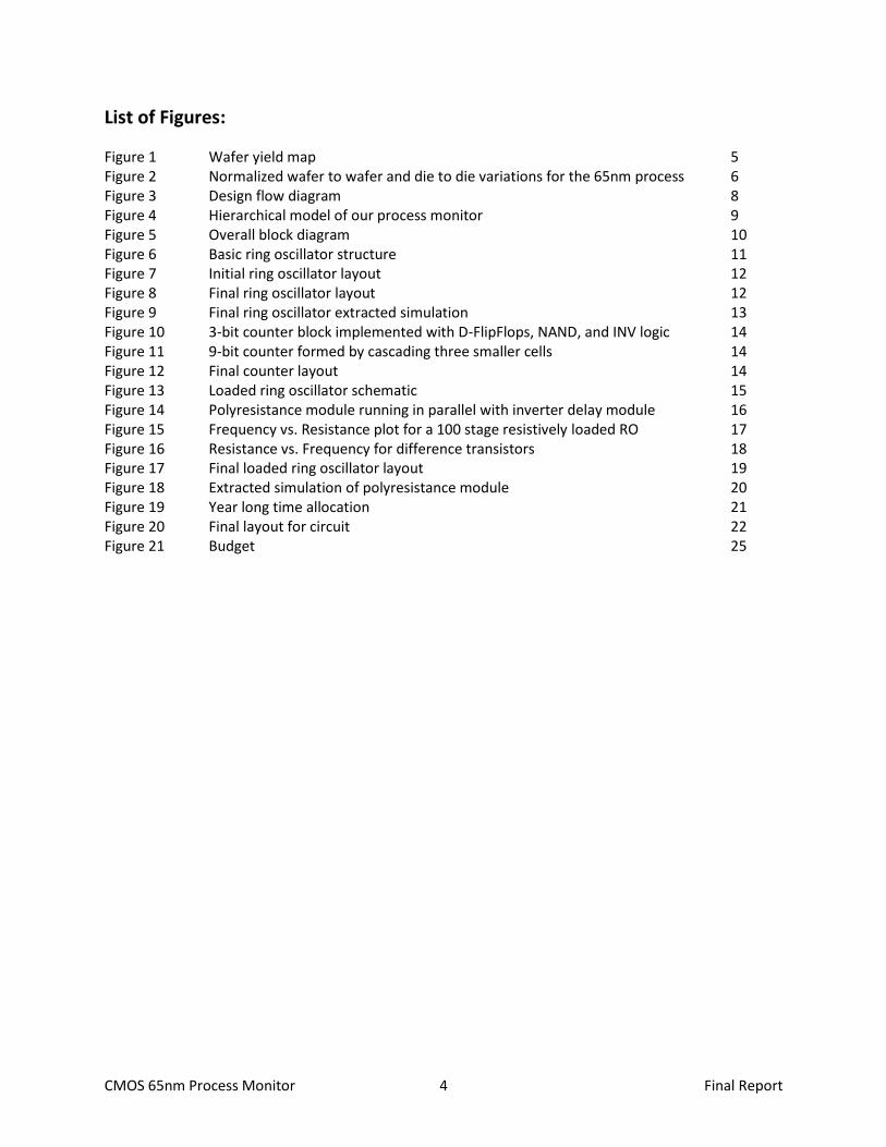
b. Inverter Delay Module: i. Background/Theory/Design: Inverter delay is a very important process variation in both digital and analog circuits. In digital circuits, fast dies can have their supply voltages lowered to conserve power, or they can be binned according to speed. For analog circuits, knowing the inverter delay provides a good starting point from which more complex parameters can be extracted. An example of this will be included in our way of measuring polyresistance. The simplest way to measure inverter delay is with a ring oscillator. By cascading inverters in series, the signal propagates through all of the stages, inverting at each stage, and then at the last stage its output is fed into the input of the first stage. When the designer uses an odd number of gates (required for an RO) the output signal that is brought back to the input is opposite the signal that initially excited the RO. This means that the signal will propagate through all of the stages again. This self continuation is why the circuit oscillates. The designer can then use a counter to count the number of times the output has changed (equal to the number of times that the signal has propagated through all of the stages) defining the frequency of the oscillator.
CMOS 65nm Process Monitor 11 Final Report
Figure 6: Basic ring oscillator structure Having a large number of stages in a ring oscillator provide two important advantages. First, it slows the frequency down to a much more manageable level. The digital logic that processes the signal often has multiple layers of gates and flip-flops which considerably slow down the maximum allowable frequency. Secondly, a large number of stages provides some measure of statistical protection. The resulting normalization ensures that the data is pertinent to the average device on the die, and not just a function of a few outlying devices. On the other hand, if the ring oscillator is too long, it will consume additional layout space and power without providing any significant improvement in performance. ii. Schematic Design: For the most part, a ring oscillator is straight forward - all it consists of is multiple inverters cascaded together in series. Traditionally, a ring oscillator is excited by a quick pulse; the problem with this design is that a pulse generator requires additional floor space and can consume large amounts of dynamic power. In our design, we use a NAND gate instead of an inverter as the first stage – one input is connected to the enable signal, and the other is connected to the feedback signal. iii. Simulation: Simulation itself is straight forward. The only real parameter of interest is the required number of stages. From our initial simulations it looked as if 50 to 100 stages would suffice for our design. We came to this conclusion because we wanted enough stages to enable our counter to function correctly as well as provide the necessary statistical normalization. At the same time, if we had too many stages, we would end up burning too much power and taking up unnecessary area. Both of these results are highly undesirable. To decide the length of our ring oscillator the first step was to complete the counter. Knowing the fastest operating frequency of the counter at all of the corners is essential to finding the length of the ring oscillator. Once our counter was completed, extracted, and tested at all corners, we tested our ring oscillator in order to find the average propagation delay through each stage. In order for the circuit to be accurate without burning additional power and size we needed to make sure that the length of the RO met this equation:
1
𝑀𝑎𝑥 𝑃𝑟𝑜𝑝𝑜𝑔𝑎𝑡𝑖𝑜𝑛 𝑇𝑟𝑜𝑢𝑔 𝑆𝑖𝑛𝑔𝑙𝑒 𝑆𝑡𝑎𝑔𝑒 ∗ 𝐿𝑒𝑛𝑔𝑡 𝑜𝑓 𝑅𝑂< 𝑀𝑖𝑛 𝐹𝑟𝑒𝑞𝑢𝑒𝑛𝑐𝑦 𝑜𝑓 𝐶𝑜𝑢𝑛𝑡𝑒𝑟

CMOS 65nm Process Monitor 12 Final Report
The final stage count that we decided on was 48 stages using both the extracted counter’s min frequency at the SS corner and the max propagation delay through a single stage at the FF counter. Although our circuit was small enough the counter and RO could never be at different corners, we felt that we could add this extra measure of safety with little additional cost. iv. Layout: There were two layouts that needed to be completed in order to create the ring oscillator. The first layout is a test layout to extract the average propagation delay through a single stage, and subsequently, the number of stages in the final test structure.
Figure 7: Initial ring oscillator design used for finding average propagation delay
Figure 8: Final ring oscillator layout
v. Final Simulation: The final simulation needs to be run using the extracted models of both the RO and the counter. The reference clock is divided down by six bits, and then used to define the length of operation for the RO. For the sample data we took, we used the mean clock frequency. Using a six bit divide down on the clock allow for an reference clock anywhere in the given range to be used without greatly affecting the accuracy of the measurement. When simulated at the various transistor corners, there is approximately a 100 count difference in both directions from the TT corner. However, there is almost no discernable difference between the TT, SF, and FS corners – confirming that we are accurately measuring the gate delay, and not relying more on one transistor type than the other.

CMOS 65nm Process Monitor 13 Final Report
Figure 9: Final extracted simulation counts with single clock frequency input
vi. Usage of Circuit: Our final ring oscillator paired with our final counter is now able to provide the information necessary to determine which of the given process corners the transistors are in. By running the circuit at a set clock input we are able to compare the number of counts to a nominal count value. If the count value is higher than the nominal value then the transistors are further towards the FF process corner. If the count value is lower than the nominal value than the transistors are further towards the SS process corner.
c. Counter: We need a high speed counter to determine the number of oscillations in our ring oscillator structures. Since the 65 nm CMOS transistors have very fast switching times, our ring oscillators are running at very high frequencies. This necessitates a fairly fast digital counter. We used a standard counting scheme and broke the counter up into 3-bit blocks. To design our counter, we found that cascading three 3-bit counters gave us reasonably fast counter without too many gates. We designed our 3-bit counters using 3-input NAND-NAND logic with minimum size transistors to give us the lowest possible propagation delay. We also used three clocked synchronous D-flip-flops to produce our sequential logic. An approximate estimate of the frequency of the ring oscillator is 1/(N*(tpLH+tpHL)). The delay time of each inverter stage is approximately 20ps, so for an 80-stage ring oscillator, the RO frequency is somewhere around 625 MHz. Therefore, our counter needs to be faster than the ring oscillator in order to correctly count the number of oscillations. We need a 9-bit counter because 29 = 512. So a 9-bit counter allows us to count 512 oscillations, this was used with the extracted layout min frequency in order to obtain the ring oscillator number of stages. The max frequency of the counter at the SS corner was 1.33 GHz. Our ring oscillator needs to have enough stages so that it does not exceed the max frequency at the SS corner.
0
100
200
300
400
500
S S T T S F F S F F
Co
un
ts
Transistor Process Corner
Inverter Only RO Counts vs. Transistor Corners for 1 Clock Cycle (48 Stages at 187MHz Clock)

CMOS 65nm Process Monitor 14 Final Report
Figure 10: 3-bit Counter Block Implemented with D-FlipFlops, NAND, and INV logic
Figure 11: 9-bit counter formed by cascading three smaller cells
Figure 12: Final Counter Layout

CMOS 65nm Process Monitor 15 Final Report
d. Polyresistance Module:
i. Theory/Design:
The second module we designed measures polyresistance variations. Specifically, we are looking at non-
silicided, doped poly-silicon . Currently, polyresistance in 65nm processes is speced at +- 20%. In reality,
the variation is usually controlled to +- 7 %, but the designer must still meet the 20% figure. Being able
to determine where the resistor are within the process would allow designers to create higher
performance circuits utilizing digital correction.
In order to enhance the isolation of the resistance parameter we plan for the module to eventually use
two different test structures and compare the results. Currently in our final circuit we have the
schematic, layout, extraction, and retest completed for the first test structure. The second test structure
is left as a continuation for the project.
The first test structure is that of a resistively loaded ring oscillator. By adding a resistive load between
the stages of the RO, we can transform resistance variation into frequency variation. The resistor in
between each of the stages pairs with the capacitance of the inverter on either side of it to create a CRC
like network. Just as in a RC network, by increasing the resistor one increases the τ, thus decreasing the
frequency.
The next issue to look at is how to isolate this resistively loaded ring oscillator in order to look at
changes in the polyresistance value and not changes in the switching speeds of the NMOS and PMOS
transistors that make up the inverter. These switching speeds are affected by changes in layer
thicknesses and in variations within the geometries. Our design accomplishes this isolation by running a
ring oscillator without resistive loading in parallel to the resistively loaded ring oscillator module. In
order to obtain our result in terms of how much the frequency has changed (leading us to the change in
resistance), we need to look at the difference between the two ring oscillator (both with the resistor
inserted in, but one with the resistor shorted out) counter values when the non loaded ring oscillator
counts as high as the counter can go (in reality we would probably let the counter count through a
couple times to get a better result with less statistical variation).
Figure 13: Loaded Ring Oscillator Schematic

CMOS 65nm Process Monitor 16 Final Report
ii. Schematic Design:
Figure 14: Polyresistance module running in parallel with inverter delay module
The way this module works is that the main control block will send a signal to the module telling it to
measure the process variation in polyresistance. The module will then turn on both of the ring
oscillators in parallel. When the ring oscillator with the resistor shorted out finishes, both of the test
structures will turn off. The value will be grabbed from the loaded ring oscillator and subtracted from
512 (since the shorted resistor RO completes one entire cycle before turning off both of the ROs). With
this difference we are now able to compare to the nominal difference and from there find out where in
the process the resistor is. In order to isolate this result from the transistor process corner, one runs the
inverter delay module in parallel in order to find out the transistor corner, than change the nominal
value based on the transistor corner.

CMOS 65nm Process Monitor 17 Final Report
iii. Simulation/Results:
Figure 15: Frequency vs. Resistance plot for a 100 stage resistively loaded RO
So, how accurate is this form of measurement and what should the starting resistor value be? To answer
this question we created a test bench schematic that included 100 inverter stages within a resistively
loaded RO pattern (the odd stage is created with an NAND gate which helps start the RO). We ran a
parametric sweep on the resistance values and measured the frequency of the oscillator. From the data
taken it is obvious that the resistance value and frequency of the RO are related linearly (proven by the
R^2 value of almost exactly 1 in our plot). This means that using a larger resistor instead of a smaller
resistor gives the designer no additional sensitivity for the measurement. Therefore it makes more sense
for our group to use a resistor value closer to 1-2kΩ instead of a larger resistor value since the smaller
resistor takes less room on the chip.
0
100
200
300
400
500
600
1 2 3 4 5 6 7 8 9 10
Fre
qu
en
cy (
MH
z)
Resistance (KΩ)
Frequency vs. Resistance (100 stage)
CMOS 65nm Process Monitor 18 Final Report
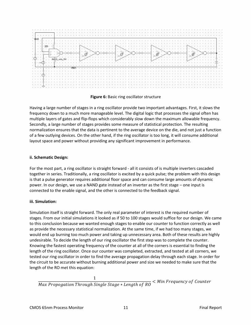
Figure 16: Resistance vs. Frequency for difference transistors
We also used this test bench with three different transistor switching speeds. It is interesting to note
that while all three have the same basic shape, there is a non-linear component between the different
switching speeds. This component is not however enough to warrant a nonlinear compensation factor in
our calculations/processing. Looking at the three corners one can see that at the value of 2k for the
resistor one gets the largest difference between the corners. This is the value that we chose for our
starting resistance within our loaded ring oscillator.
iv. Layout
Now that we have a schematic that works based on spice simulations the next step is to complete the
layout in order to obtain an extracted circuit. The layout of the loaded ring oscillator is interesting
because we needed to be able to isolate our measurement from parasitic elements as much as possible.
In order to do this we decided to complete the layout for our loaded ring oscillator and then copy it but
short the resistor out. This gave us two ROs but with one shorting all of the resistors out. This helps limit
the amount of parasitic elements outside of the resistor corner.

CMOS 65nm Process Monitor 19 Final Report
Figure 17: Layout for both ring oscillators (left: loaded, right: non-loaded (shorted resistor))
v. Final Simulation
With the extracted circuit we ran both ring oscillators at all corners until the resistively loaded RO with
the resistors shorted completed through all 512 counts. At this time we took the value from the loaded
RO and subtracted from 512 its count. This gave us our difference. The plot of our difference for all
corners is displayed below.
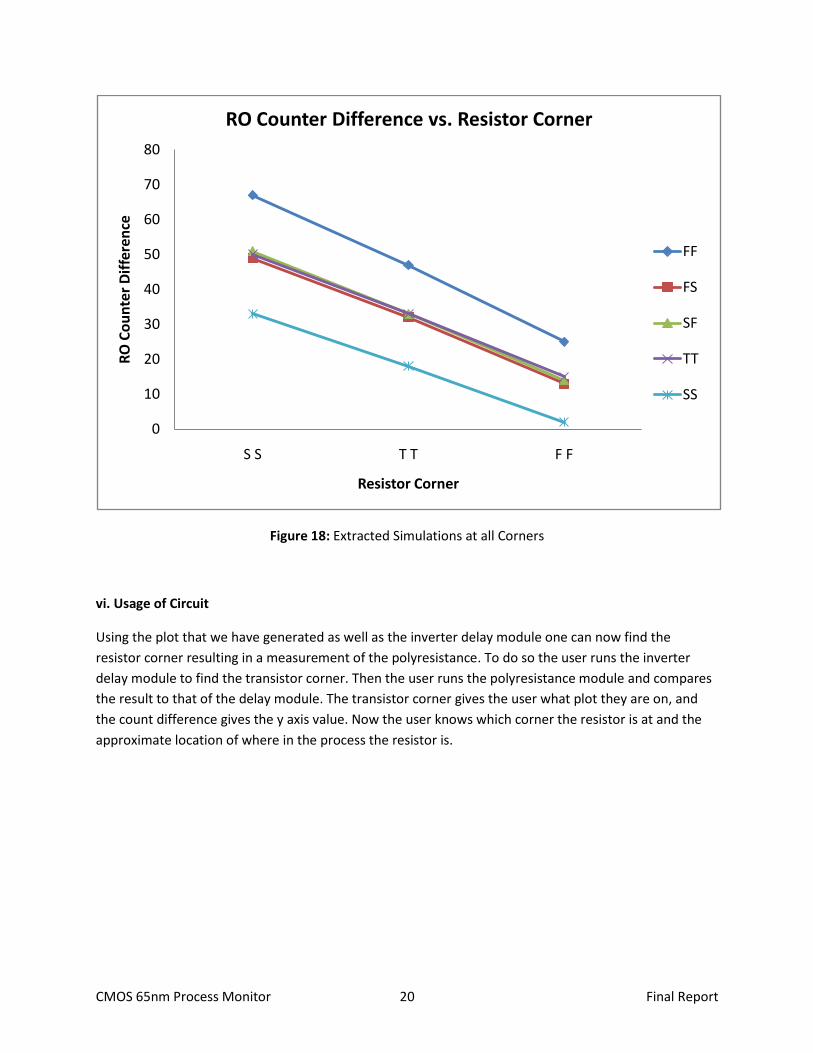
CMOS 65nm Process Monitor 20 Final Report
Figure 18: Extracted Simulations at all Corners
vi. Usage of Circuit
Using the plot that we have generated as well as the inverter delay module one can now find the
resistor corner resulting in a measurement of the polyresistance. To do so the user runs the inverter
delay module to find the transistor corner. Then the user runs the polyresistance module and compares
the result to that of the delay module. The transistor corner gives the user what plot they are on, and
the count difference gives the y axis value. Now the user knows which corner the resistor is at and the
approximate location of where in the process the resistor is.
0
10
20
30
40
50
60
70
80
S S T T F F
RO
Co
un
ter
Dif
fere
nce
Resistor Corner
RO Counter Difference vs. Resistor Corner
FF
FS
SF
TT
SS

CMOS 65nm Process Monitor 21 Final Report
IV. Conclusion/Future Work:
As of right now we have two working modules. Both modules have been completed in terms of
schematic, initial testing, layout, extraction, and post extraction test. We have also begun work on the
digital control logic, and various sections are in different stages of completion. All simulation data in this
paper was generated using extracted circuit blocks.
The digital control logic for both the input and the output needs to be finalized for the entire module. The digital processing logic needs to be calibrated. The top level layout connections need to be completed and tested. Our goals for continuing the project would be to finish the control logic and complete additional measurement blocks. The polyresistance module needs another test structure to isolate capacitance variation out of the measurement, and a threshold variation module would also prove very useful. Looking back on our timeline we feel that we have followed it fairly closely despite the slow start at the beginning of the year due to lack of tools and the learning curve required in order to become proficient with the tools.
Figure 19: Year long time allocation

CMOS 65nm Process Monitor 22 Final Report
Figure 20: Final Layout

CMOS 65nm Process Monitor 23 Final Report
V. Acknowledgements: We would like to thank Mr. Brian Misek for sharing his wisdom in IC design. We would also like to thank Dr. Hugh Grinolds for his semester-long guidance and support. And of course, we are very grateful that Avago Technologies supported our design project and provided us with access to their IC design tools and libraries. Also, Charles Thangaraj from the CSU VLSI Lab was patient in answering our countless questions.
VI. Bibliography:
1. Phillip E. Allen & Douglas R. Holberg, CMOS Analog Circuit Design, 2nd ed. , Oxford University
Press, USA, January 12th, 2002.
2. RJ Baker, CMOS Circuit Design, Layout, and Simulation, 2nd ed. , Wiley-IEEE Press, November
9th, 2007.
3. Neil Weste, Principles of CMOS VLSI Design, 1st ed. , Addison-Wesley Publishing, 1984.
4. J. Keane, T. Kim, and C.H. Kim, "Silicon Odometers: On-Chip Test Structures for Monitoring
Reliability Mechanisms and Sources of Variation", Workshop on Test Structure Design for
Variability Characterization, Nov. 2008
5. Manoj Sachdev, Defect-oriented testing for nano-metric CMOS VLSI circuits, 2nd ed.,
Dordrecht:Springer 2007

CMOS 65nm Process Monitor 24 Final Report
Appendix #1: Abbreviations: MOSFET – Metal-Oxide-Semiconductor Field Effect Transistor CMOS – Complementary Metal-Oxide-Semiconductor PMOS – P Channel MOSFET NMOS - N Channel MOSFET RO – Ring Oscillator FF - Fast PMOS, Fast NMOS (refers to gate delay variation) SS - Slow PMOS, Slow NMOS FS – Fast PMOS, Slow NMOS SF – Slow PMOS, Fast NMOS TT – Typical PMOS, Typical NMOS PTAT – Proportional to Absolute Temperature

CMOS 65nm Process Monitor 25 Final Report
Appendix #2: Budget:
Our budget for the year is very static. To start off, the school has allocated each team member in the
group $50. This gives our team of three people a total of $150. For second semester we were allocated
another $150. This gives us a total of $300 to spend for the year. Luckily, since our project was in
conjunction with Avago there was no need for the money we have been allocated for our senior design.
Avago has provided us with not only the models, but use of their libraries, their tools, and even their
facilities and computers. This gives our team one less thing to worry about since we don’t need to spend
the time looking for sponsors. It is also important because without Avago we would not have been able
to do our designs in the 65nm process. This is due to the models simply being too expensive as well as
the full software suite required to do simulations with the models. On top of all the donations Avago has
given us there is also a chance that our process variation monitor might go out on one of their test
wafers later this year. Without this space being donated we would never have been able to fund a test
wafer on our budget. We probably wouldn’t have even been able to get enough donations to pay for a
test wafer. Overall, thanks to Avago we have everything needed for our project including a rare
undergraduate opportunity to have our circuit be fabricated on a test wafer. We are on-time, under size
and under budget.
Figure 21: Budget
$0
$50
$100
$150
$200
$250
$300
$350
Budget


![65nm CMOS Process Technology - Fujitsu · 65nm CMOS Process Technology Paul Kim Senior Manager, Foundry Services Fujitsu Microelectronics America, Inc. ... [nm] 0 500 400 300 200](https://static.fdocuments.in/doc/165x107/5c63c41809d3f2ad198bc41b/65nm-cmos-process-technology-65nm-cmos-process-technology-paul-kim-senior.jpg)