
Clocking Methodology and Flip-Flops -...
29
Transcript of Clocking Methodology and Flip-Flops -...
2
Overview
• Reading– Rabaey, Chapter 7– W&H, 7.3-7.4
• Overview– Given that clock(s) of known phases are distributed to each storage
element, the goal of a clocking methodology is to maintain timing correlation between data (or control). Interestingly, we do not need to know when the boundary is, just that there is a regular one.
– The idea is to slow down the fast signal to the boundary.– We will briefly review different methodologies: edge-triggered
(single-phase), 2-phase latch-based, single-phase latch-based.– In particular, we will focus on the design of the synchronizing
elements, the F/F and Latches. As we will see, the goals of the design depends on the application.
3
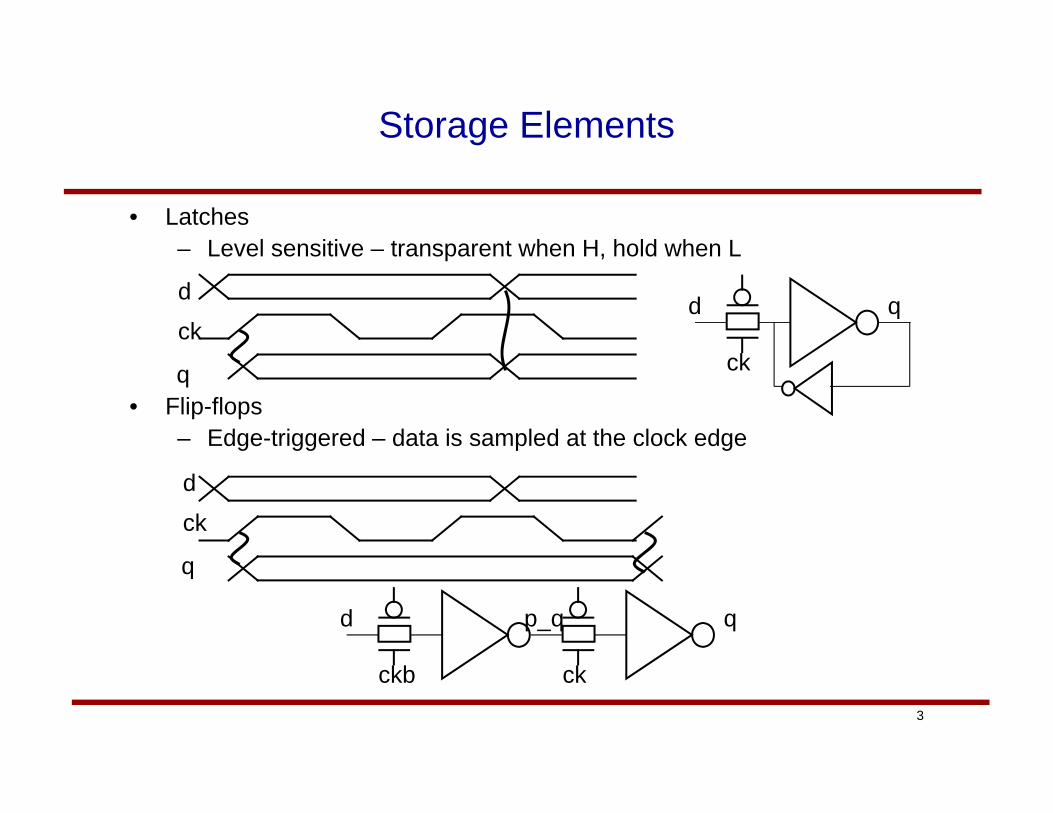
Storage Elements
• Latches– Level sensitive – transparent when H, hold when L
• Flip-flops– Edge-triggered – data is sampled at the clock edge
ck
qdck
q
d
ckb
d
ck
qp_q
ck
q
d
4
Characteristics of Storage Elements
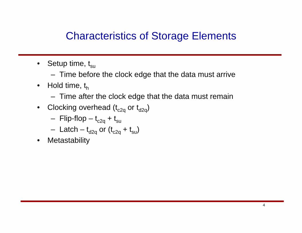
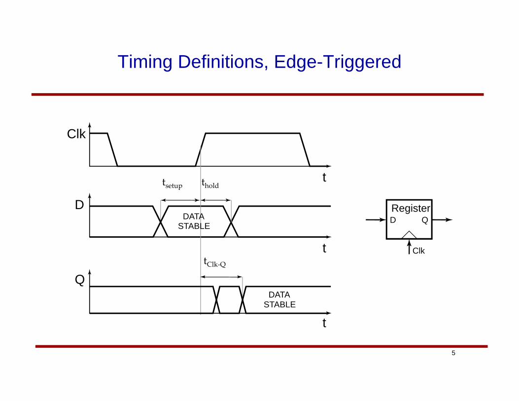
• Setup time, tsu
– Time before the clock edge that the data must arrive • Hold time, th
– Time after the clock edge that the data must remain • Clocking overhead (tc2q or td2q)
– Flip-flop – tc2q + tsu
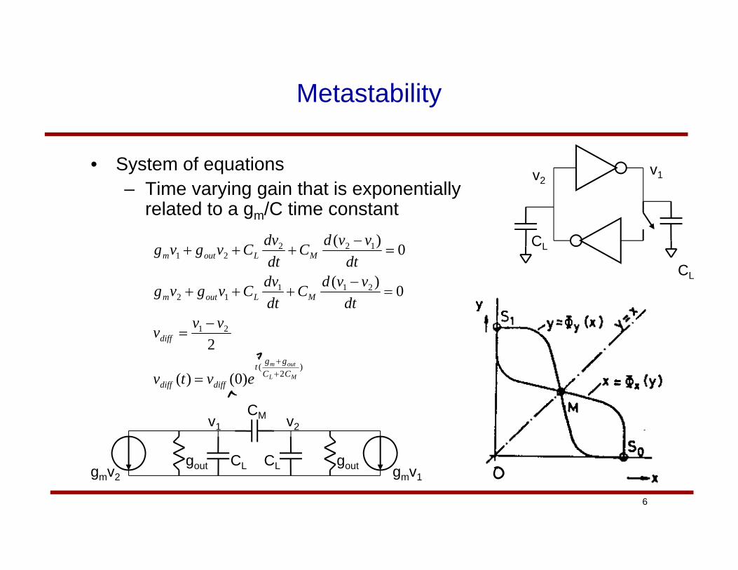
– Latch – td2q or (tc2q + tsu)• Metastability
5
Timing Definitions, Edge-Triggered
t
Clk
t
D
t
QDATA
STABLE
DATASTABLE
Register
Clk
D Q
tsetup thold
tClk‐Q
6
Metastability
• System of equations– Time varying gain that is exponentially
related to a gm/C time constant
CL
CL
v1v2
v1 v2
gmv2 gmv1gout CL
CM
CL gout
)2
(
21
21112
12221
)0()(
2
0)(
0)(
ML
outmCCggt
diffdiff
diff
MLoutm
MLoutm
evtv
vvv
dtvvdC
dtdvCvgvg
dtvvdC
dtdvCvgvg
7
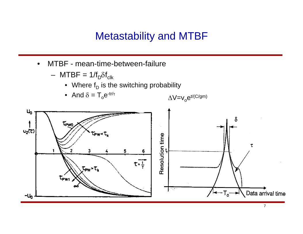
Metastability and MTBF
• MTBF - mean-time-between-failure– MTBF = 1/fDfclk
• Where fD is the switching probability• And = Toe-tr/
V=voet/(C/gm)
8
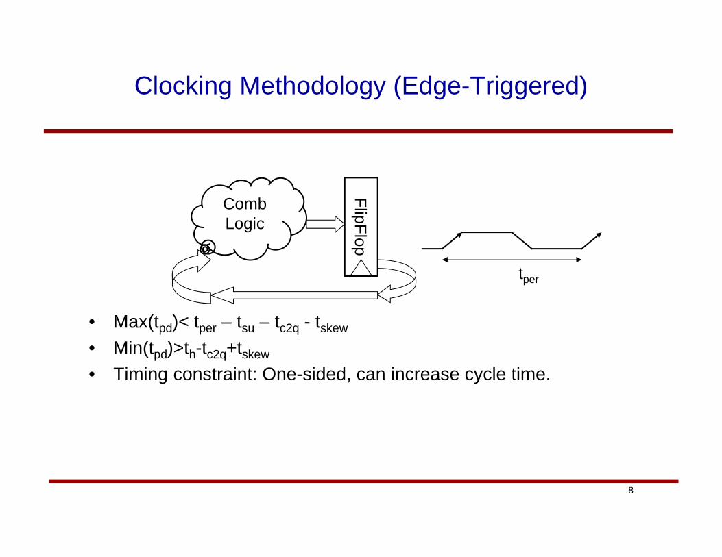
Clocking Methodology (Edge-Triggered)
• Max(tpd)< tper – tsu – tc2q - tskew
• Min(tpd)>th-tc2q+tskew
• Timing constraint: One-sided, can increase cycle time.
CombLogic
FlipFlop
tper
9
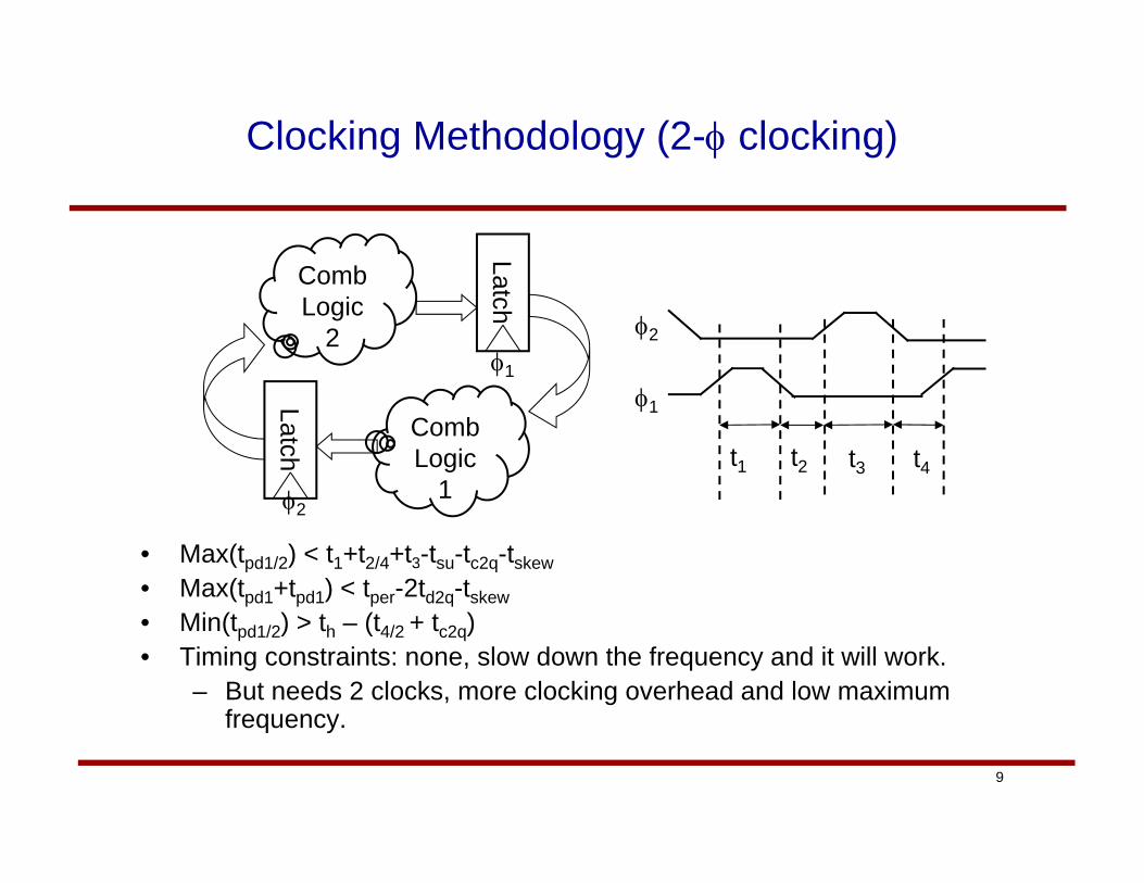
Clocking Methodology (2- clocking)
• Max(tpd1/2) < t1+t2/4+t3-tsu-tc2q-tskew• Max(tpd1+tpd1) < tper-2td2q-tskew• Min(tpd1/2) > th – (t4/2 + tc2q)• Timing constraints: none, slow down the frequency and it will work.
– But needs 2 clocks, more clocking overhead and low maximum frequency.
CombLogic
2
Latch
CombLogic
1
Latch
1
2
t1 t2 t3 t4
1
2
10
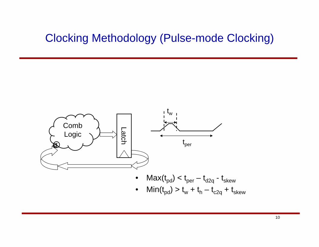
Clocking Methodology (Pulse-mode Clocking)
• Max(tpd) < tper – td2q - tskew
• Min(tpd) > tw + th – tc2q + tskew
CombLogic
Latch tper
tw
11
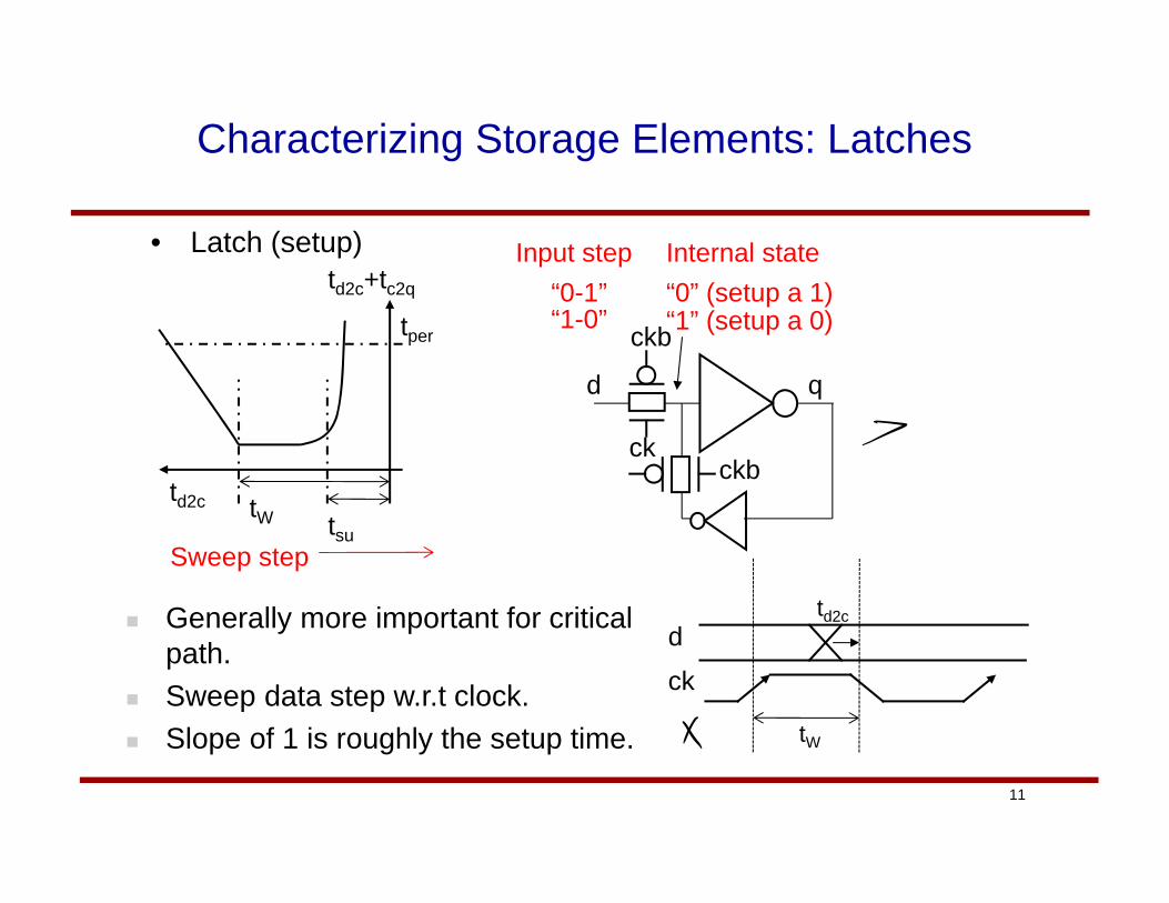
Characterizing Storage Elements: Latches
td2c
td2c+tc2q
tsutW
tper
ck
d
• Latch (setup)
Generally more important for critical path.
Sweep data step w.r.t clock. Slope of 1 is roughly the setup time.
ck
qd
ckb
ckb
td2c
tW
“0” (setup a 1)“0-1”“1” (setup a 0)“1-0”
Input step Internal state
Sweep step
12
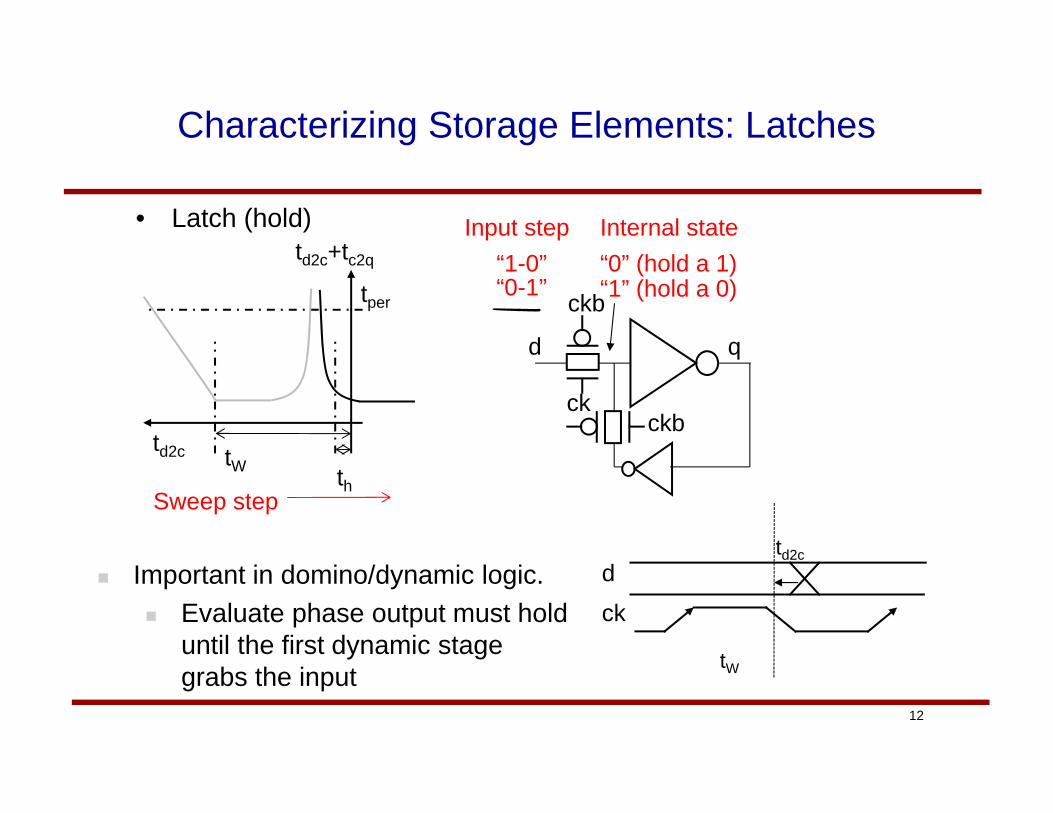
Characterizing Storage Elements: Latches
td2c
td2c+tc2q
thtW
tper
ck
d
• Latch (hold)
Important in domino/dynamic logic. Evaluate phase output must hold
until the first dynamic stage grabs the input
ck
qd
ckb
ckb
td2c
tW
“0” (hold a 1)“1-0”“1” (hold a 0)“0-1”
Input step Internal state
Sweep step
13
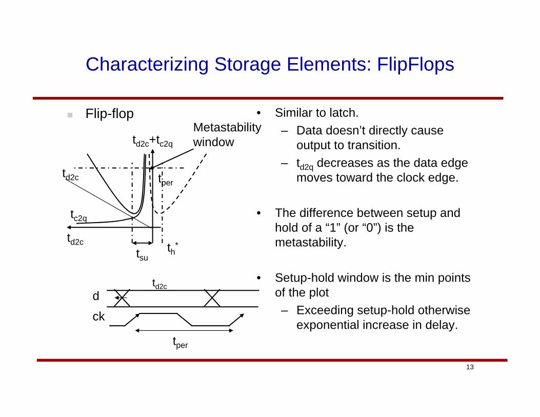
Characterizing Storage Elements: FlipFlops
• Similar to latch.– Data doesn’t directly cause
output to transition.– td2q decreases as the data edge
moves toward the clock edge.
• The difference between setup and hold of a “1” (or “0”) is the metastability.
• Setup-hold window is the min points of the plot– Exceeding setup-hold otherwise
exponential increase in delay.
td2c+tc2q
td2ctsu
tper
Flip-flopMetastabilitywindow
th*
ck
dtd2c
tper
tc2q
td2c
14
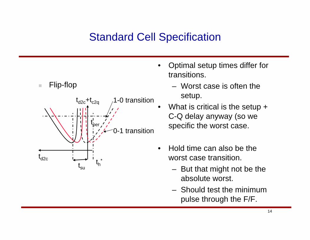
Standard Cell Specification
• Optimal setup times differ for transitions.– Worst case is often the
setup.• What is critical is the setup +
C-Q delay anyway (so we specific the worst case.
• Hold time can also be the worst case transition.– But that might not be the
absolute worst.– Should test the minimum
pulse through the F/F.
td2c+tc2q
td2ctsu
tper
Flip-flop
0-1 transition
th*
1-0 transition
15
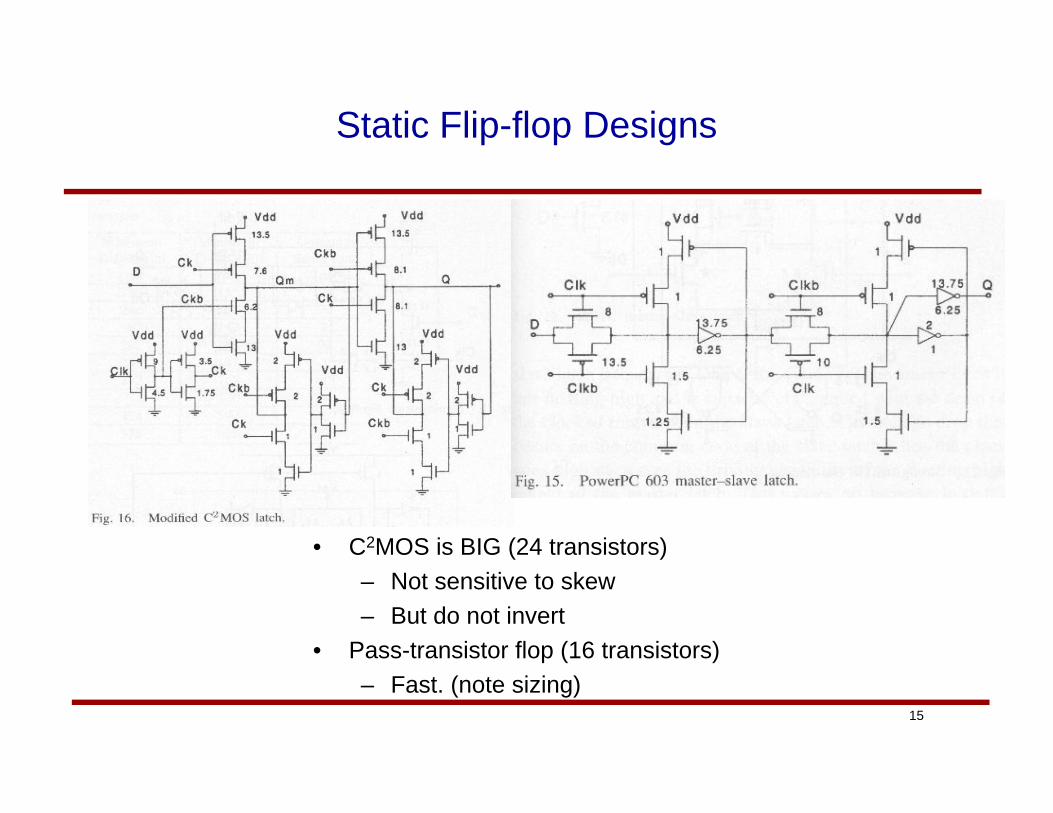
Static Flip-flop Designs
• C2MOS is BIG (24 transistors)– Not sensitive to skew– But do not invert
• Pass-transistor flop (16 transistors)– Fast. (note sizing)
16
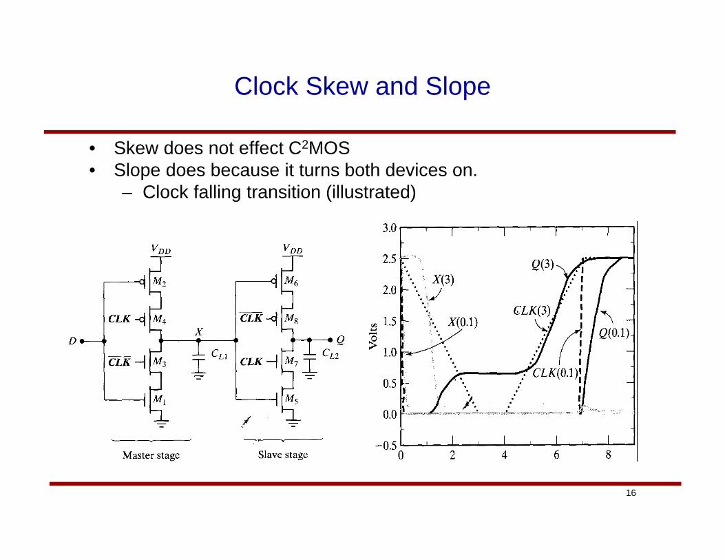
Clock Skew and Slope
• Skew does not effect C2MOS• Slope does because it turns both devices on.
– Clock falling transition (illustrated)
17
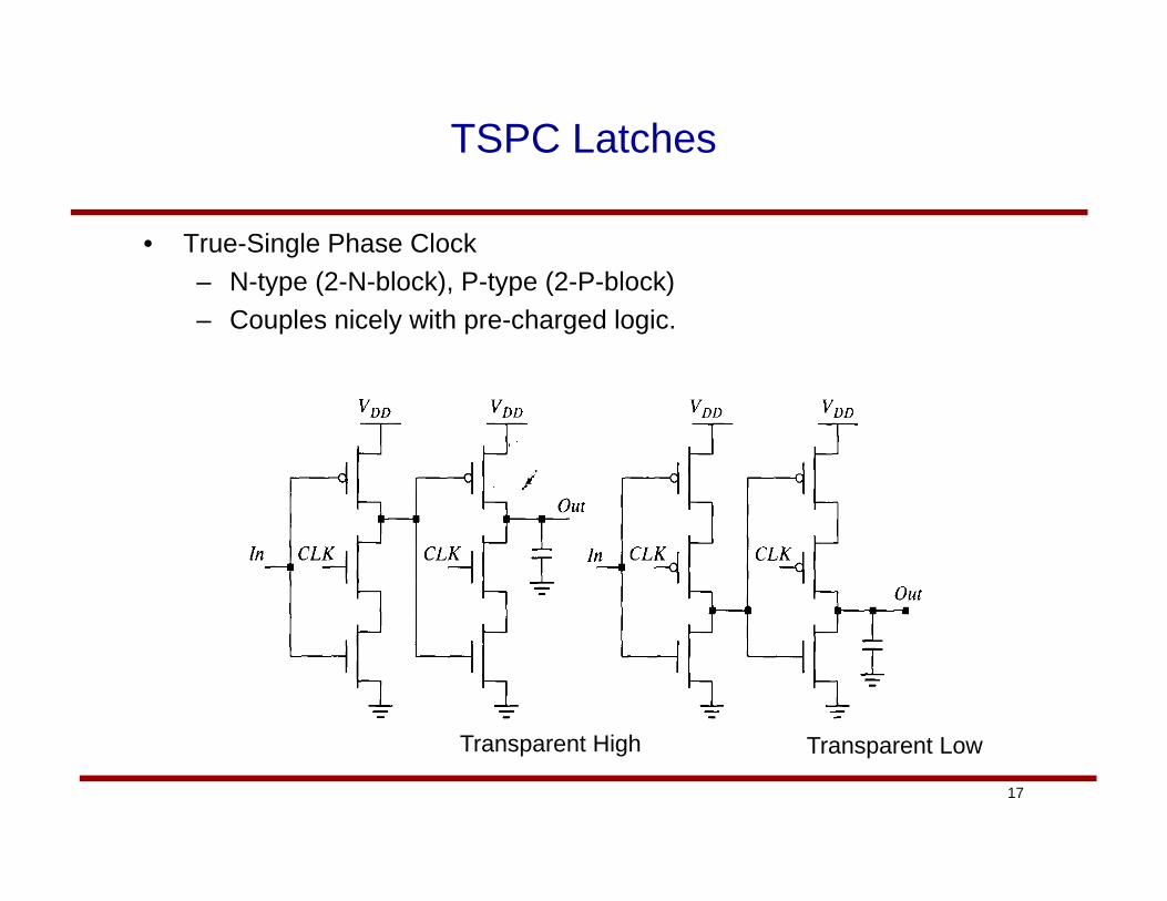
TSPC Latches
• True-Single Phase Clock – N-type (2-N-block), P-type (2-P-block)– Couples nicely with pre-charged logic.
Transparent High Transparent Low
18
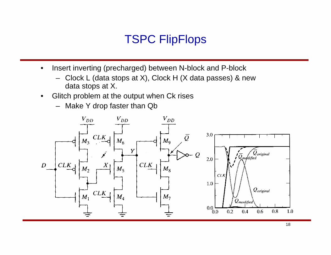
TSPC FlipFlops
• Insert inverting (precharged) between N-block and P-block– Clock L (data stops at X), Clock H (X data passes) & new
data stops at X.• Glitch problem at the output when Ck rises
– Make Y drop faster than Qb
19
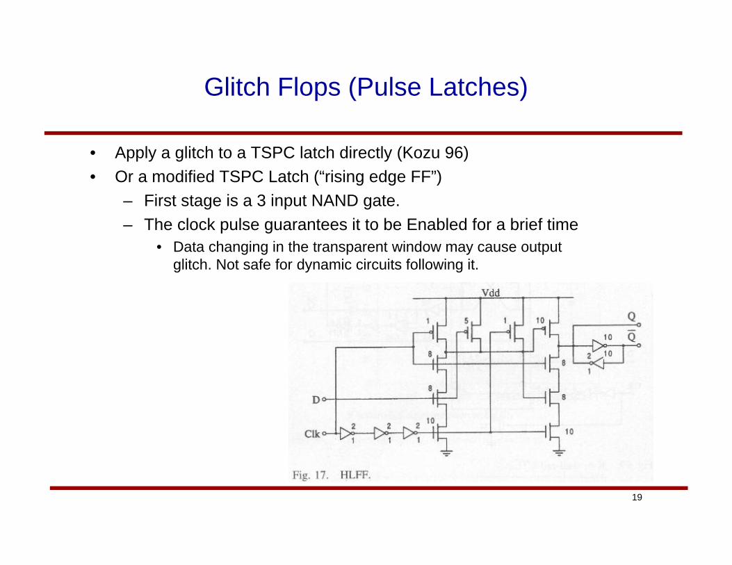
Glitch Flops (Pulse Latches)
• Apply a glitch to a TSPC latch directly (Kozu 96)• Or a modified TSPC Latch (“rising edge FF”)
– First stage is a 3 input NAND gate.– The clock pulse guarantees it to be Enabled for a brief time
• Data changing in the transparent window may cause output glitch. Not safe for dynamic circuits following it.
20
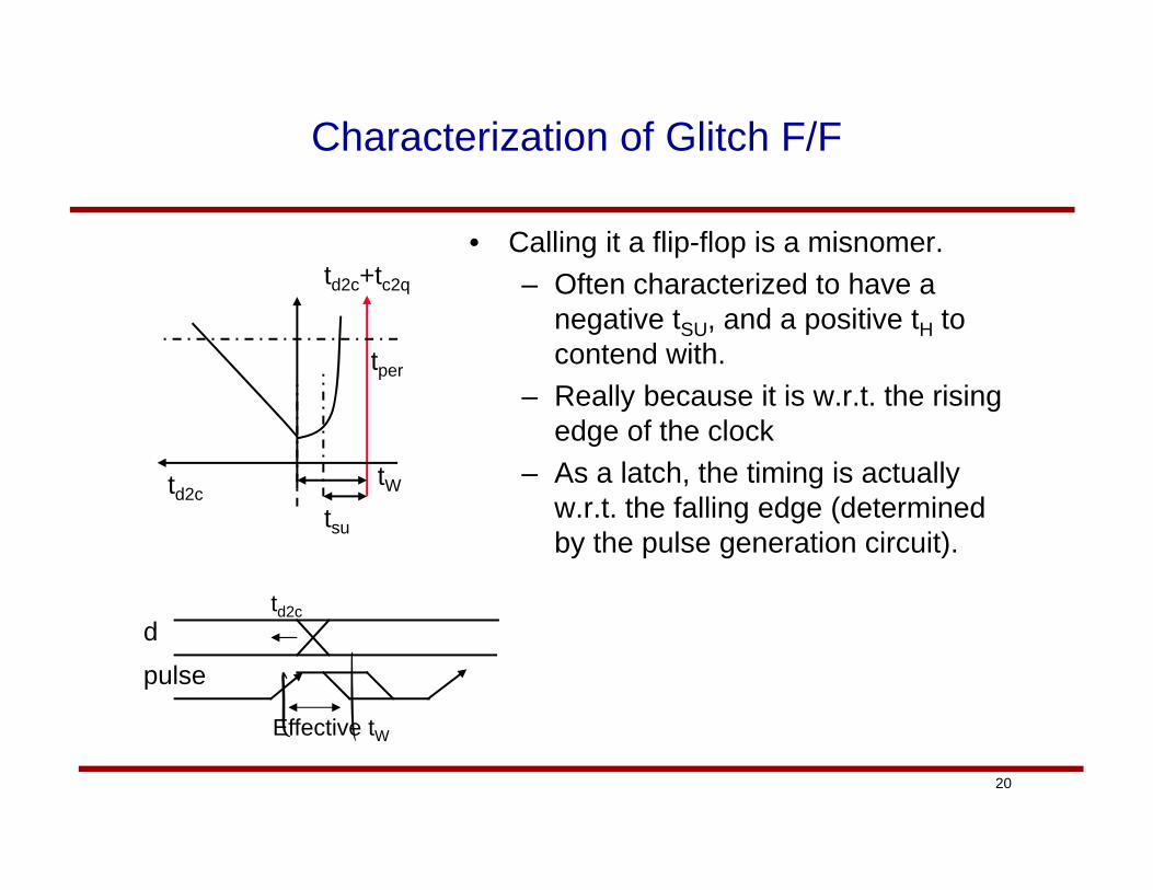
Characterization of Glitch F/F
• Calling it a flip-flop is a misnomer. – Often characterized to have a
negative tSU, and a positive tH to contend with.
– Really because it is w.r.t. the rising edge of the clock
– As a latch, the timing is actually w.r.t. the falling edge (determined by the pulse generation circuit).
td2c
td2c+tc2q
tsu
tW
tper
pulse
dtd2c
Effective tW
21
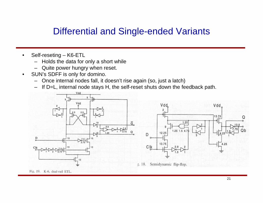
Differential and Single-ended Variants
• Self-reseting – K6-ETL– Holds the data for only a short while– Quite power hungry when reset.
• SUN’s SDFF is only for domino.– Once internal nodes fall, it doesn’t rise again (so, just a latch)– If D=L, internal node stays H, the self-reset shuts down the feedback path.
22
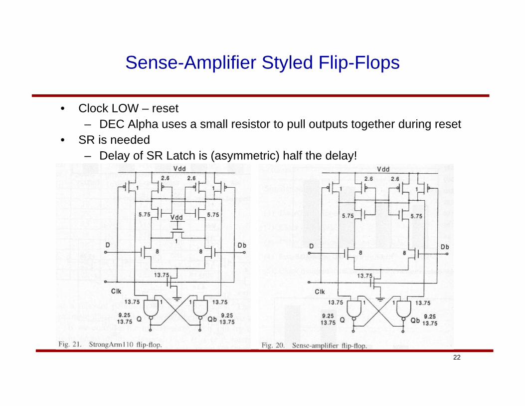
Sense-Amplifier Styled Flip-Flops
• Clock LOW – reset– DEC Alpha uses a small resistor to pull outputs together during reset
• SR is needed– Delay of SR Latch is (asymmetric) half the delay!
23
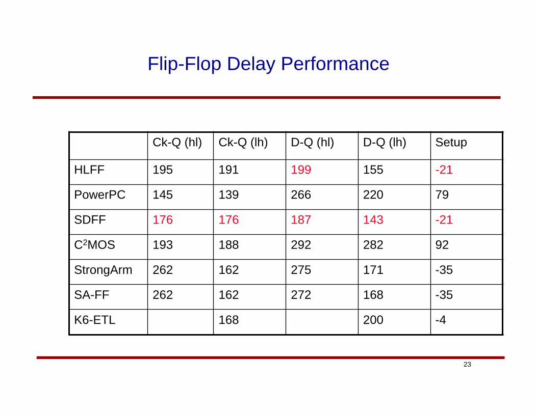
Flip-Flop Delay Performance
Ck-Q (hl) Ck-Q (lh) D-Q (hl) D-Q (lh) Setup
HLFF 195 191 199 155 -21
PowerPC 145 139 266 220 79
SDFF 176 176 187 143 -21
C2MOS 193 188 292 282 92
StrongArm 262 162 275 171 -35
SA-FF 262 162 272 168 -35
K6-ETL 168 200 -4
24
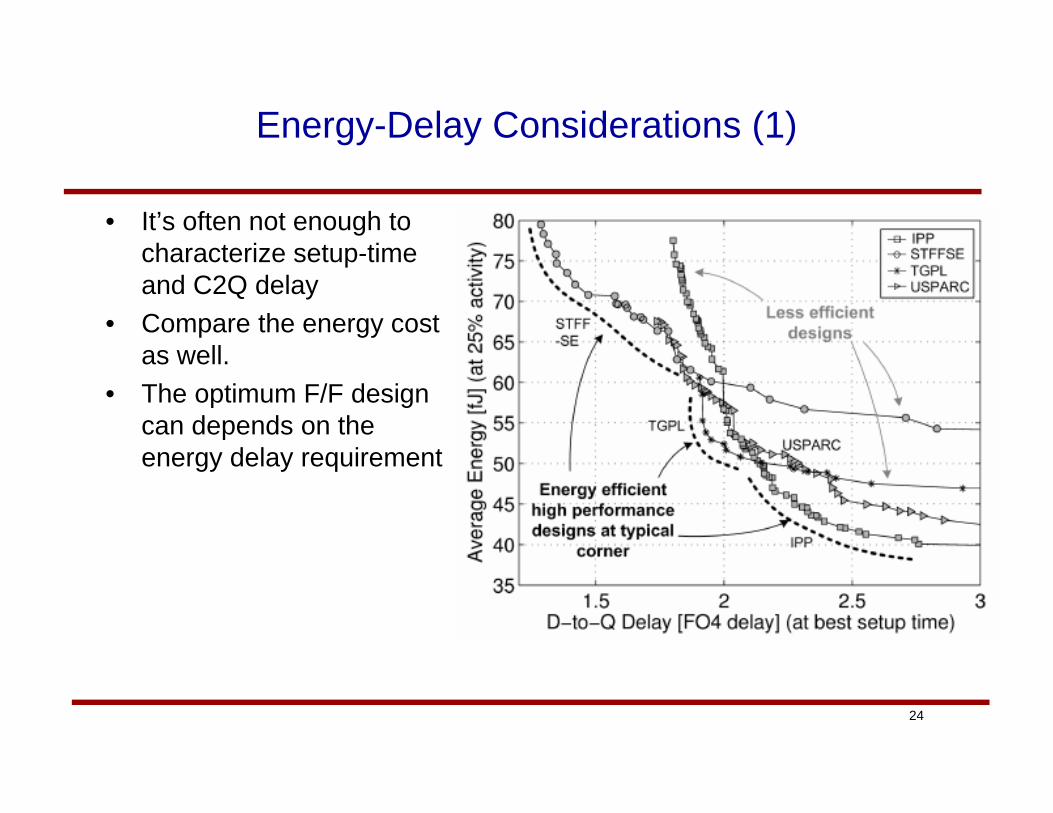
Energy-Delay Considerations (1)
• It’s often not enough to characterize setup-time and C2Q delay
• Compare the energy cost as well.
• The optimum F/F design can depends on the energy delay requirement
25
Energy-Delay Considerations (2)
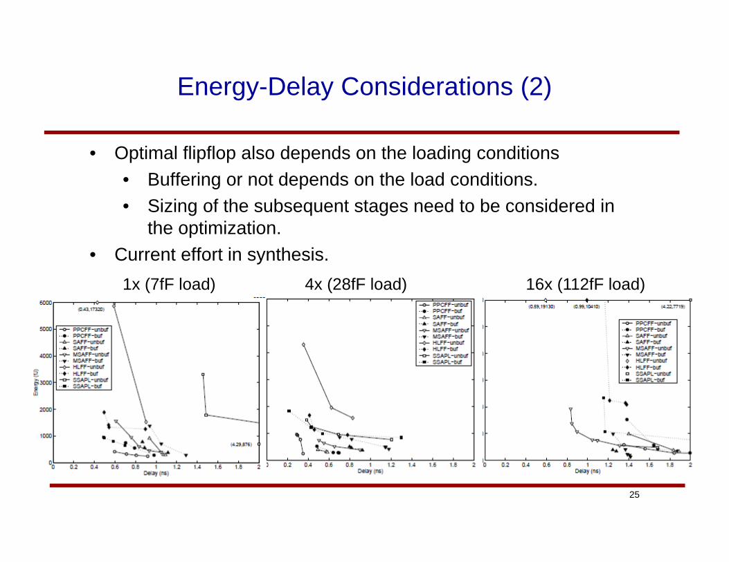
1x (7fF load) 4x (28fF load) 16x (112fF load)
• Optimal flipflop also depends on the loading conditions• Buffering or not depends on the load conditions.• Sizing of the subsequent stages need to be considered in
the optimization.• Current effort in synthesis.
26
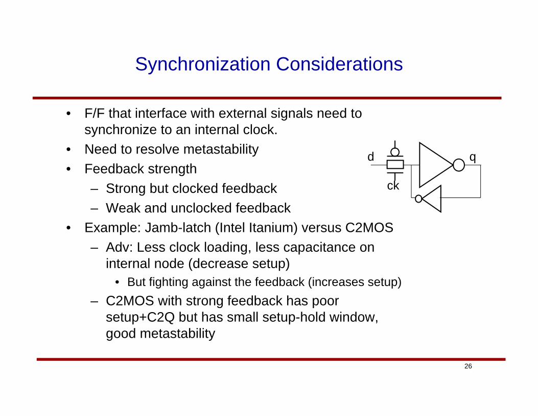
Synchronization Considerations
• F/F that interface with external signals need to synchronize to an internal clock.
• Need to resolve metastability• Feedback strength
– Strong but clocked feedback– Weak and unclocked feedback
• Example: Jamb-latch (Intel Itanium) versus C2MOS – Adv: Less clock loading, less capacitance on
internal node (decrease setup)• But fighting against the feedback (increases setup)
– C2MOS with strong feedback has poor setup+C2Q but has small setup-hold window, good metastability
ck
qd
27
Recent Designs (1)
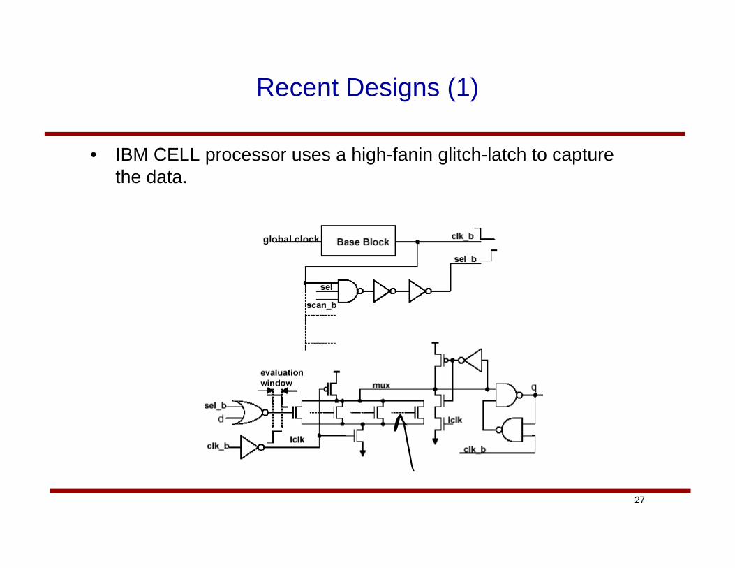
• IBM CELL processor uses a high-fanin glitch-latch to capture the data.
28
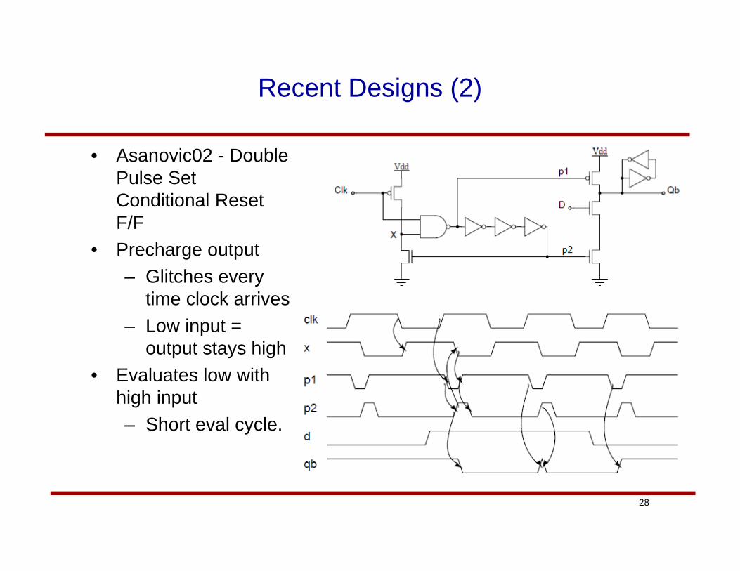
Recent Designs (2)
• Asanovic02 - Double Pulse Set Conditional Reset F/F
• Precharge output– Glitches every
time clock arrives– Low input =
output stays high• Evaluates low with
high input– Short eval cycle.
29
Summary
• Storage elements are an important part of logic design.• They can represent 5-10% of the total latency cost per cycle
– 1-2FO4 delays out of 20 FO4 delay per cycle in a high-performance design.
– Latches have lower overhead so pulsed latches are the dominant design approach.
• Critical path consideration is primarily setup+C2Q delay• Energy efficiency considerations however can lead of a design
space that varies the choice of F/F or latch.• Other design criteria such as MTBF for a synchronizer can push
a design toward yet other directions.