CLOCK CONSTRUCTED USING THE 555 OSCILLATOR
20
CLOCK CONSTRUCTED USING THE 555 OSCILLATOR Shih-Ping Hu Department of Mechanical Engineering Hungkuo Delin University of Technology Taipei, Taiwan 236, R.O.C. Key Words: astable multistage oscillator, equal duty time, mod 60, mod 24. ABSTRACT In the 21st century, the world has become a place where every second counts. We must finish whatever we need to finish within a specified amount of time. The routines of work have become very important for modern people. In an industry, the precise control of hours, minutes and seconds has a huge influences on the quality of goods produced during the industrial production process. For example, the precise control of the cooling time in a steel furnace has an influence on the rigidity and the ductility of the produced steel, the control of the firing time for ceramic arts affects the aesthetics and durability of the artworks, the control of the fusion time for the production of alloy steel affects its internal grain structure and strength, etc. This paper can be divided into two parts. In the first part, we intro- duce the 555 astable multistage oscillator. The external circuit of the os- cillator is adjusted to match the one-way behavior of the diode, allowing the oscillator to output digital pulses with an equal duty cycle. The sec- ond part we describe a digital clock composed of two mod 60 and one mod 24 counter. When the digital pulse wave output from the first part of the oscillator is transmitted to the second part, the second part of the digital clock starts to function. I. INTRODUCTION The 555 astable multistage oscillator [1] described in the first part of this paper is a hybrid timer composed of a comparator [1], an SR flip-flop [2], a BJT transistor [1], a resistor divider [3] and an inverter [3]. This type of equipment is commonly used in time control and wave- form generators, which are cheap and accurate. The sec- ond part introduces a digital clock composed of a combi- nation of two mod 60 and one mod 24 counter with other logic ICs. The biggest contribution of the novel device design described in this paper is that a function generator is no longer needed in oscillation clocks. II. LITERATURE REVIEW We can find examples in the literature related to the study of oscillation clocks. In Cai [4] researched and analyzed a low-power phase noise CMOS complementary LC resonant voltage controlled oscillator. The advantage of this method is that it saves power and eliminates unnec- essary noise, but its disadvantage is that it uses all analog electronic components, causing insufficient stability. In Lin [5] studied the research and design of low-voltage wide- range adjustment voltage-controlled oscillators and negative resistance voltage-controlled oscillators. The 技術學刊 第三十五卷 第一期 民國一○九年 1 Journal of Technology, Vol. 35, No. 1, pp. 1-20 (2020) *Corresponding author: Shih-Ping Hu, e-mail: [email protected]
Transcript of CLOCK CONSTRUCTED USING THE 555 OSCILLATOR
CLOCK CONSTRUCTED USING THE 555 OSCILLATOR
Shih-Ping Hu
Department of Mechanical Engineering Hungkuo Delin University of Technology
Taipei, Taiwan 236, R.O.C.
Key Words: astable multistage oscillator, equal duty time, mod 60, mod
24.
ABSTRACT
In the 21st century, the world has become a place where every second
counts. We must finish whatever we need to finish within a specified
amount of time. The routines of work have become very important for
modern people. In an industry, the precise control of hours, minutes and
seconds has a huge influences on the quality of goods produced during the
industrial production process. For example, the precise control of the
cooling time in a steel furnace has an influence on the rigidity and the
ductility of the produced steel, the control of the firing time for ceramic arts
affects the aesthetics and durability of the artworks, the control of the
fusion time for the production of alloy steel affects its internal grain
structure and strength, etc.
This paper can be divided into two parts. In the first part, we intro-
duce the 555 astable multistage oscillator. The external circuit of the os-
cillator is adjusted to match the one-way behavior of the diode, allowing
the oscillator to output digital pulses with an equal duty cycle. The sec-
ond part we describe a digital clock composed of two mod 60 and one mod
24 counter. When the digital pulse wave output from the first part of the
oscillator is transmitted to the second part, the second part of the digital
clock starts to function.
I. INTRODUCTION
The 555 astable multistage oscillator [1] described in
the first part of this paper is a hybrid timer composed of a
comparator [1], an SR flip-flop [2], a BJT transistor [1], a
resistor divider [3] and an inverter [3]. This type of
equipment is commonly used in time control and wave-
form generators, which are cheap and accurate. The sec-
ond part introduces a digital clock composed of a combi-
nation of two mod 60 and one mod 24 counter with other
logic ICs. The biggest contribution of the novel device
design described in this paper is that a function generator
is no longer needed in oscillation clocks.
II. LITERATURE REVIEW
We can find examples in the literature related to the
study of oscillation clocks. In Cai [4] researched and
analyzed a low-power phase noise CMOS complementary
LC resonant voltage controlled oscillator. The advantage
of this method is that it saves power and eliminates unnec-
essary noise, but its disadvantage is that it uses all analog
electronic components, causing insufficient stability. In
Lin [5] studied the research and design of low-voltage
wide- range adjustment voltage-controlled oscillators and
negative resistance voltage-controlled oscillators. The
技術學刊 第三十五卷 第一期 民國一○九年 1
Journal of Technology, Vol. 35, No. 1, pp. 1-20 (2020)
*Corresponding author: Shih-Ping Hu, e-mail: [email protected]

2 Journal of Technology, Vol. 35, No. 1
7-segment LED(d)
7447 (d)
7447 (b)
7490 (d)
7408 (d)
7447 (a)
7408 (b)
7432 (b)
7432 (d)
7447 (c)
7490 (c)
a
133
4
5
16
12
6 2 1 7
12
9
8
11
1076
3
2
1
14
5
7490 (d)
12
9
8
11
1076
3
2
1
14
5
1110 915 14
b c d e f g
7-segment LED(b)
a b c d e f g
7-segment LED(c)
a
a bfga bfg
e d ce d c
b c d e f g
a b c d e f g
16345
7
12
9
8
11
5
1076
3
2
1
14
7490 (a)
48
7
6
2 5
3CK
0.01�F100�F
1
555
RA1
RA2
RB1
RB2
C
D
2.2K
12
9
8
11
5
1076
3
2
1
14
1268
B A
200�×7
13 12 1110 915 14
13 1211 10 9 1514
7-segment LED(a)
a b c d e f g
3
71268
4
5
16
13 12 1110 9 15 14
a bfga bfg
e d ce d c
147
147
sw
147
147
6165438 2 1 7
200�×7
200�×2
200�×7
200�×7
200�×2
5K�
2.2K�
5K�
Fig. 1 Global electric circuit diagram (I)
Hu. S-P.: Clock constructed using the 555 oscillator 3
a bfga bfg
e d c e d c
7-segment LED(e)
7447 (e)
7490 (e)
7408 (f)
7432 (f)
7404
4
147
3
a
138
16
5
4 3
12
621
1
5
6
7
714
1 2
3
1 2
3
4 5
6
6
7404
4
32 6
10K2K1
CK2 Q2
J27
5
1214
1
Q2
CK1 Q1
J1
7473
Q1
9
CL1 CL2
11
12
7 14
4
5
9
8
10
13
12 11
A
10 2 3 14
8
B
9
12
11
7
11 10 9 15 14
b c d e f g
7-segment (f)
7447 (f)
a
1316
5 4 3
12
628 7 1
11 10 9 15 14
b c d e f g
200�×7
200�200�
200�×7
Fig. 2 Global electric circuit diagram (II)
4 Journal of Technology, Vol. 35, No. 1
transient to
Vcc = + 5
RA = RA1 + RA2
7.2k�
t
(sec)
7.2k� 555
a
b
3
512
c
c d
e
V3(t)
Vout
V3
Vcc
7
6
8 4
Vc(t)
100�F
0.01�F+
-
RB
Fig. 3 The current path for first charging
advantage of this method is that the applicable frequency
width can be changed through voltage regulation, while
the disadvantage is that the structure is complicated and it
is easy to make errors. In Huang [6] designed a low-power
LC voltage controlled oscillator using substrate bias and
quality factor improvement techniques.
The advantage of this design is that the voltage regu-
lator is combined with the simplest inductor L and capaci-
tor C. However, the disadvantage is that the stability is
not sufficient. Furthermore, when an error occurs, it is
not easy to detect it. In Chang [7] studied the use of
clock gate replication technology to construct a clock tree.
The advantage of this method is that it can be com-
posed of only basic logic gates, but its disadvantage is that
the digital circuit is too complicated.
III. EXPLANATION OF PRINCIPLES
1. The electronic components used in the design de-
scribed in this paper are; (1) logic IC 74LS90X5,
74LS47X6, 74LS08X3, 74LS32X3,74LS04X1,
74LS73X1, IC555; (2) resistance (1/4 w), 200�X48,
5K�X2, 2.2K�X2 (3) capacitance (50w), 100μFX1,
0.01μFX1; (4) diode (number: IN4001) X1; (5)
common anode seven segment LED display (number:
HS-5101BS3-1207) X6; (6) LED light X1; (7) circuit
board (number E10-108) X1.
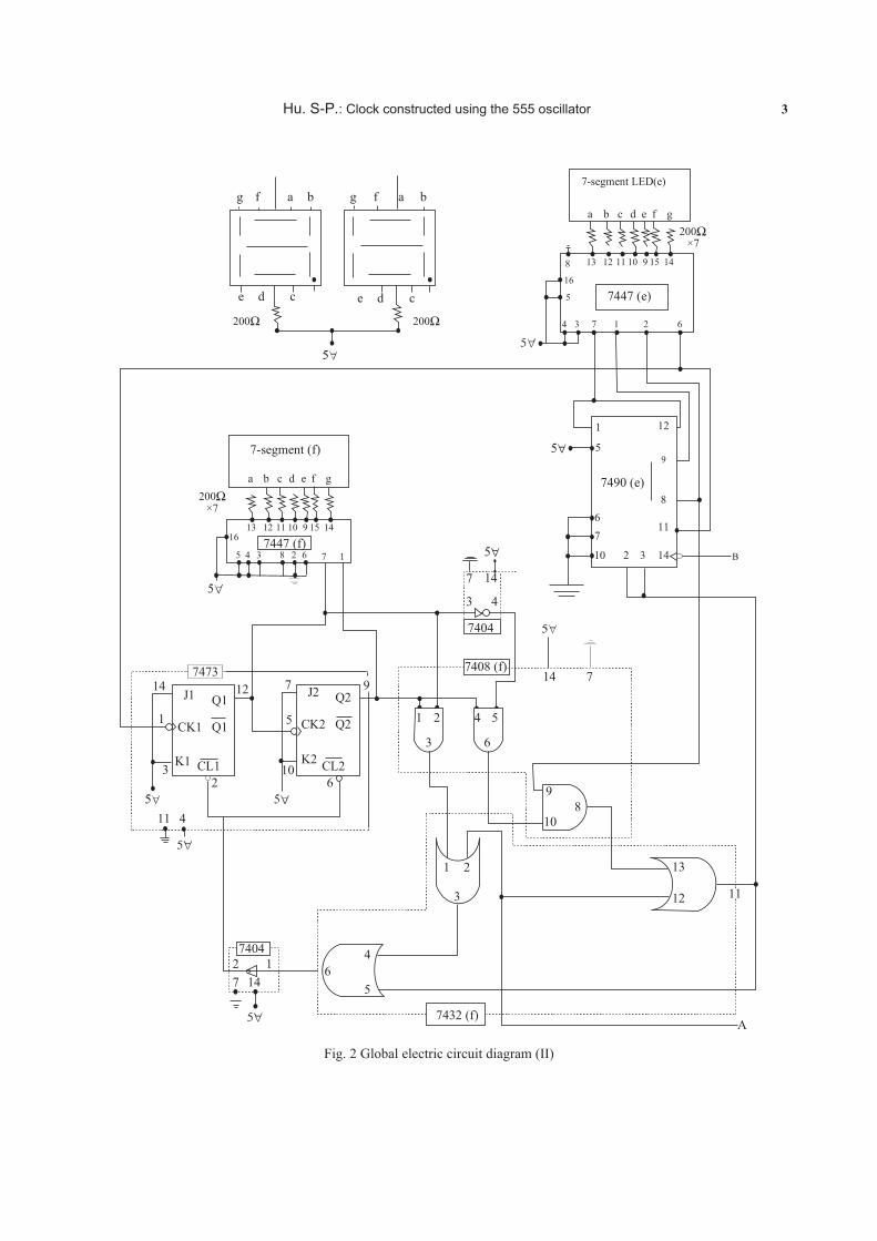
2. All wiring diagrams are shown in Fig. 1 and Fig. 2.
555
transient to
RA = 7.2k�
7.2k�
b
D
c
d
a
2 15
6
t
3
8 4
Vout
Vc(t)100�F
0.01�F+
-
V3
(sec)
V3(t)
Vcc
0
t1e
Vcc = + 5
RB
Fig. 4 The current path for discharging
The point of convergence in these two diagrams is
indicated by A and B, respectively. In other words,
point A in Fig. 1 must be connected to point A in Fig.
2, and point B in figure 1 must be connected to point
B in Fig. 2.
3. The external wiring diagram of the 555 astable multi-
stage oscillator is shown in Fig. 1.
4. In Fig. 1, the 7490 (a) and 7447 (a) LED displays (a)
are used to show the seconds in the ones’ place. The
7490 (b) and 7447 (b) LED displays (b) are used to
show the seconds in the tens’ place.
5. In Fig. 1, the 7490(c) and 7447(c) LED displays (c)
are used to show the minutes in the ones’ place. The
7490(d) and 7447(d) LED display (d) are used to
show the minutes in the tens’ place.
6. In Fig. 2, the 7490(e) and 7447(e) LED displays (e)
are used to show the hours in the ones’ place. The
7473 and 7447(f) LED displays (f) are used to show
the hours in the tens’ place.
7. In Fig. 3, the broken line represents the path through
which the charging current travels. At point a, the
current path has two different path choices, but RB =
RB1 + RB2 = 7.2 K� >> RD = 5�, so the charging cur-
rent must pass from the diode without going over RB.
At the same time, the output voltage V3 (Vout) of the
555 oscillator is the DC bias Vcc of the oscillator (Vcc
= 5V). Since Fig. 3 is where the first charge occurs,
then the time it takes is transient and is expressed by
t0 (sec).
8. In Fig. 4, the solid line delineates the path through
which the discharging current travels. Because the

Hu. S-P.: Clock constructed using the 555 oscillator 5
Vcc = + 5
7
e
8 4
36
2 15
7.2k� 555
b
c
c
7.2k�
+
-Vc(t)
100�F
0.01�F
RB
RA
t0 t1 t2
t
V2
0
V3(t)
D
Vcc
Vout
Fig. 5 The current path for second charging
V3(t)
Vcc
t0
t(sec)
0.5 0.5 0.5 0.5
T = 1 secT = 1 sec
0
Fig. 6 Output pulse of 555 oscillator
diode is turned off, the discharging current has only
one choice at point d, that is, it flows through RB but
does not flow through the diode. At the same time, the
output voltage V3 (Vout) of the 555 oscillator is at the
low potential “0” (V3 = Vout = 0 V); the time is t1 (sec).
9. The time t1 required for the discharge based on the
resistance RB through which the discharge current
path in Fig. 4 passes is calculated by:
t1 = RBC × ln2 = (7.2X10³�) × (100X10-6F) × ln2 = 5 (sec).
10. For the second charge, the charging current path is the
same as for the first charge, as shown in Fig. 5. The
time t2 required for the second charge can be calcu-
lated as follows:
t2 = RAC × ln2 = (7.2X10³�) × (100X10-6F) × ln2 =
0.5 (sec)
The charge times after the second charge are all the
same as t2 = 0.5 (sec)
11. The output pulse of the 555 astable multistage oscil-
lator after the second charge is shown in Fig. 6. In
Fig. 6, the rests of the pulse waves are steady except
for the first charge transient. The periods (T) of all
waves are 1 sec.
T = t1 + t1 = 0.5 + 0.5 = 1 (sec) frequency f = 1 / T = 1 / 1 = 1 (Hz)
12. The output voltage V3 (Vout) in Fig. 5 is connected to
the 14th pin of the logic IC7490 (a) in figure 1 as the
input digital pulse wave for the entire clock.
IV. THE DETAILED PRINCIPLES OF THE LOGIC CIRCUIT
1. A switch (SW) is used to reset the clock in this design.
When SW = / (high potential) (5V), the clock is set to
zero hours, zero minutes and zero seconds. Its logic
circuit is shown in Fig. 7. At the same time, although
the digital pulse of the 555 oscillator continues to be
transmitted to CK7, IC7490 (a) is still unable to be ac-
tivated. Thus, CK6 - CK1 do not receive any signal
and all the LED displays still denote the same time 00 :
00 : 00.
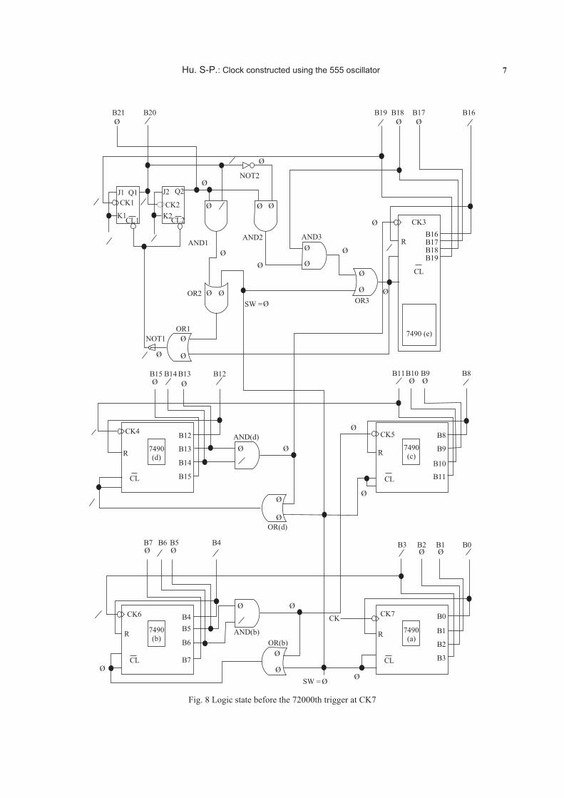
2. SW = Ø (grounding). The status of CK7 before the
72000th trigger is shown in Fig. 8. The LED display
denotes 19 : 59 : 59.
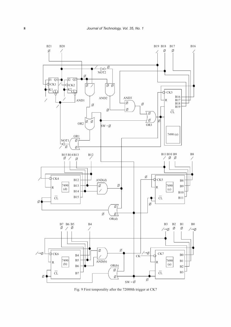
3. SW = Ø (grounding). The first temporality after the
72000th trigger at CK7 is shown in Fig. 9. At this
temporality, 7490 (a) is reset to zero, that is, B3 : / →
Ø and B0 : / → Ø. At the same time, because B3 : /
→ Ø, it promotes CK6: / → Ø (negative edge trigger).
The LED display denotes 19 : 59 : 50.
4. SW = Ø (grounding). The second temporality after
the 72000th trigger at CK7 is shown in Fig. 10. Be-
cause CK6 : / → Ø (negative edge trigger), it causes
7490 (b) to move forward. Thus, B5 : Ø → / , B4: /
→ Ø. The LED display denotes 19 : 59 : 60.
5. SW = Ø (grounding). The third temporality after the
72000th trigger at CK7 is shown in Fig. 11. Because
the AND (b) gate output is / (high potential), therefore
the OR (b) gate output is / (high potential) and CK5
becomes / (high potential). The LED displays denote
19 : 59 : 60.
6 Journal of Technology, Vol. 35, No. 1
B21 B20 B19
Ø ØØ Ø Ø Ø
NOT2
NOT1
B15
B15
B14
B14
B13
B13
B12
B7
B7
B6
B6
B5
B5
B4
B4
B12
B11
B11
B10
B10
B9
B9
B8
B3
B3
B2
B2
B1
B1
B0
B0
B8
AND1 AND2 AND3B16
CK3
CK5CK4
RR
OR3
OR(d)
OR(b)
AND(d)
AND(b)
OR2
OR1
SW = 1
SW = 1
R B17B18B19
B18 B17 B16
K2
CK2
J2 Q2
clear
clear
clear
CK7
R
clear
clear
CK6
R
clear
7490 (e)
7490(c)
7490(a)
7490(b)
7490(d)
clearK1
CK1
J1 Q1
Ø
Ø
ØØØØ
ØØØØ ØØØØ
ØØØØ
Fig. 7 Logic diagram for the case of SW=1(5V)
Hu. S-P.: Clock constructed using the 555 oscillator 7
Ø
Ø Ø
Ø
Ø
Ø
Ø
ØØ
Ø
Ø
Ø
Ø Ø
Ø
Ø
ØØ
Ø Ø
Ø
Ø
Ø Ø
Ø
Ø
Ø
Ø
Ø
Ø
Ø
Ø
Ø
ØØ
ØØØ
Ø
Ø
Ø
Ø ØØ
B21 B20 B19
NOT2
NOT1
B15
B15
B14
B14
B13
B13
B12
B7
B7
B6
B6
B5
B5
B4
B4
B12
B11
B11
B10
B10
B9
B9
B8
B3
B3
B2
B2
B1
B1
B0
B0
B8
AND1AND2 AND3 B16
CK3
CK5CK4
RR
OR3
OR(d)
OR(b)
AND(d)
AND(b)
OR2
OR1
SW =
SW =
R B17B18B19
B18 B17 B16
K2CL2
CK2
J2 Q2
CL
CK7CK
R
CL
CL
CK6
R
CL
7490 (e)
7490(c)
7490(a)
7490(b)
7490(d)
CL1K1
CK1
J1 Q1
CL
Fig. 8 Logic state before the 72000th trigger at CK7
8 Journal of Technology, Vol. 35, No. 1
B21 B20 B19
NOT2
NOT1
B15
B15
B14
B14
B13
B13
B12
B7
B7
B6
B6
B5
B5
B4
B4
B12
B11
B11
B10
B10
B9
B9
B8
B3
CK
B3
B2
B2
B1
B1
B0
B0
B8
AND1AND2 AND3 B16
CK3
CK5CK4
RR
OR3
OR(d)
OR(b)
AND(d)
AND(b)
OR2
OR1
SW =
SW =
R B17B18B19
B18 B17 B16
K2CL2
CK2
J2 Q2
CL
CL
CK7
R
CL
CL
CK6
R
CL
7490 (e)
7490(c)
7490(a)
7490(b)
7490(d)
CL1K1
CK1
J1 Q1
Fig. 9 First temporality after the 72000th trigger at CK7
Hu. S-P.: Clock constructed using the 555 oscillator 9
B21 B20 B19
NOT2
NOT1
B15
B15
B14
B14
B13
B13
B12
B7
B7
B6
B6
B5
B5
B4
B4
B12
B11
B11
B10
B10
B9
B9
B8
B3
CK
B3
B2
B2
B1
B1
B0
B0
B8
AND1 AND2 AND3 B16
CK3
CK5CK4
RR
OR3
OR(d)
OR(b)
AND(d)
AND(b)
OR2
OR1
SW =
SW =
R B17B18B19
B18 B17 B16
K2CL2
CK2
J2 Q2
CL
CL
CK7
R
CL
CL
CK6
R
CL
7490 (e)
7490(c)
7490(a)
7490(b)
7490(d)
CL1K1
CK1
J1 Q1
Fig. 10 Second temporality after the 72000th trigger at CK7
10 Journal of Technology, Vol. 35, No. 1
B21 B20 B19
NOT2
NOT1
B15
B15
B14
B14
B13
B13
B12
B7
B7
B6
B6
B5
B5
B4
B4
B12
B11
B11
B10
B10
B9
B9
B8
B3
B3
B2
B2
B1
B1
B0
B0
B8
AND1 AND2 AND3B16
CK3
CK5CK4
RR
OR3
OR(d)
OR(b)
AND(d)
AND(b)
OR2
OR1
SW =
SW =
R B17B18B19
B18 B17 B16
K2CL2
CK2
J2 Q2
CL
CL
CK7
R
CL
CL
CK6
R
7490 (e)
7490(c)
7490(a)
7490(b)
7490(d)
CL1K1
CK1
J1 Q1
CK
Fig. 11 Third temporality after the 72000th trigger at CK7
Hu. S-P.: Clock constructed using the 555 oscillator 11
Ø
Ø
Ø
Ø
Ø
Ø
Ø
Ø Ø Ø Ø
Ø
Ø
Ø Ø Ø Ø
Ø
Ø
Ø Ø
ØØØ
Ø
Ø
Ø
Ø
Ø
Ø
Ø
ØØ
ØØØ
Ø
Ø
Ø
Ø ØØ
B21 B20 B19
NOT2
NOT1
B15
B15
B14
B14
B13
B13
B12
B7
B7
B6
B6
B5
B5
B4
B4
B12
B11
B11
B10
B10
B9
B9
B8
B3
B3
B2
B2
B1
B1
B0
B0
B8
AND1 AND2 AND3B16
CK3
CK5CK4
RR
OR3
OR(d)
OR(b)
AND(d)
AND(b)
OR2
OR1
SW =
SW =
R B17B18B19
B18 B17 B16
K2CL2
CK2
J2 Q2
CL
CL
CK7CK
R
CL
CL
CK6
R
clear
7490 (e)
7490(c)
7490(a)
7490(b)
7490(d)
CL1K1
CK1
J1 Q1
Fig. 12 Fourth temporality after the 72000th trigger at CK7
12 Journal of Technology, Vol. 35, No. 1
B21 B20 B19
NOT2
NOT1
B15
B15
B14
B14
B13
B13
B12
B7
B7
B6
B6
B5
B5
B4
B4
B12
B11
B11
B10
B10
B9
B9
B8
B3
B3
B2
B2
B1
B1
B0
B0
B8
AND1 AND2 AND3B16
CK3
CK5CK4
RR
OR3
OR(d)
OR(b)
AND(d)
AND(b)
OR2
OR1
SW =
SW =
R B17B18B19
B18 B17 B16
K2CL2
CK2
J2 Q2
CL
CL
CK7CK
R
CL
CL
CK6
R
CL
7490 (e)
7490(c)
7490(a)
7490(b)
7490(d)
CL1K1
CK1
J1 Q1
Fig. 13 Fifth temporality after the 72000th trigger at CK7
Hu. S-P.: Clock constructed using the 555 oscillator 13
B21 B20 B19
NOT2
NOT1
B15
B15
B14
B14
B13
B13
B12
B7
B7
B6
B6
B5
B5
B4
B4
B12
B11
B11
B10
B10
B9
B9
B8
B3
B3
B2
B2
B1
B1
B0
B0
B8
AND1 AND2 AND3 B16
CK3
CK5CK4
RR
OR3
OR(d)
OR(b)
AND(d)
AND(b)
OR2
OR1
SW =
SW =
CK
R B17B18B19
B18 B17 B16
K2CL2
CK2
J2 Q2
CL
CL
CK7
R
CL
CL
CK6
R
CL
7490 (e)
7490(c)
7490(a)
7490(b)
7490(d)
CL1K1
CK1
J1 Q1
Fig. 14 Sixth temporality after the 72000th trigger at CK7
14 Journal of Technology, Vol. 35, No. 1
B21 B20 B19
NOT2
NOT1
B15
B15
B14
B14
B13
B13
B12
B7
B7
B6
B6
B5
B5
B4
B4
B12
B11
B11
B10
B10
B9
B9
B8
B3
B3
B2
B2
B1
B1
B0
B0
B8
AND1 AND2 AND3B16
CK3
CK5CK4
RR
OR3
OR(d)
OR(b)
AND(d)
AND(b)
OR2
OR1
SW =
SW =
R B17B18B19
B18 B17 B16
K2CL2
CK2
J2 Q2
CL
CL
CK7
R
CK
CL
clear
CK6
R
CL
7490 (e)
7490(c)
7490(a)
7490(b)
7490(d)
CL1K1
CK1
J1 Q1
Fig. 15 Seventh temporality after the 72000th trigger at CK7
Hu. S-P.: Clock constructed using the 555 oscillator 15
B21 B20 B19
NOT2
NOT1
B15
B15
B14
B14
B13
B13
B12
B7
B7
B6
B6
B5
B5
B4
B4
B12
B11
B11
B10
B10
B9
B9
B8
B3
B3
B2
B2
B1
B1
B0
B0
B8
AND1 AND2 AND3 B16
CK3
CK5CK4
RR
OR3
OR(d)
OR(b)
AND(d)
AND(b)
OR2
OR1
SW =
SW =
R B17B18B19
B18 B17 B16
K2CL2
CK2
J2 Q2
CL
CL
CK7
R
CK
CL
clear
CK6
R
CL
7490 (e)
7490(c)
7490(a)
7490(b)
7490(d)
CL1K1
CK1
J1 Q1
Fig. 16 Eighth temporality after the 72000th trigger at CK7

16 Journal of Technology, Vol. 35, No. 1
Ø
Ø
Ø
Ø Ø
Ø
Ø
Ø Ø Ø
Ø
Ø Ø ØØ
Ø ØØ Ø Ø
ØØ
Ø
Ø
Ø
Ø
Ø
Ø
Ø
ØØ
ØØØ
Ø
Ø
Ø
Ø ØØ
Ø
Ø
Ø Ø
B21 B20 B19
NOT2
NOT1
B15
B15
B14
B14
B13
B13
B12
B7
B7
B6
B6
B5
B5
B4
B4
B12
B11
B11
B10
B10
B9
B9
B8
B3
B3
B2
B2
B1
B1
B0
B0
B8
AND1 AND2 AND3B16
CK3
CK5CK4
RR
OR3
OR(d)
OR(b)
AND(d)
AND(b)
OR2
OR1
SW =
SW =
R B17B18B19
B18 B17 B16
K2CL2
CK2
J2 Q2
CL
CL
CK7
R
CK
CL
CL
CK6
R
CL
7490 (e)
7490(c)
7490(a)
7490(b)
7490(d)
CL1K1
CK1
J1 Q1
Fig. 17 Ninth temporality after the 72000th trigger at CK7

Hu. S-P.: Clock constructed using the 555 oscillator 17
Ø
Ø
Ø Ø
Ø Ø Ø
Ø
Ø Ø ØØ
Ø ØØ Ø Ø
ØØ
Ø
Ø
Ø
Ø
Ø
Ø ØØ
Ø
Ø
Ø ØØ
Ø
B21 B20 B19
NOT2
NOT1
B15
B15
B14
B14
B13
B13
B12
B7
B7
B6
B6
B5
B5
B4
B4
B12
B11
B11
B10
B10
B9
B9
B8
B3
B3
B2
B2
B1
B1
B0
B0
B8
AND1 AND2 AND3 B16
CK3
CK5CK4
RR
OR3
OR(d)
OR(b)
AND(d)
AND(b)
OR2
OR1
SW =
SW =
R B17B18B19
B18 B17 B16
K2CL2
CK2
J2 Q2
CL
CL
CK7
R
CK
CL
CL
CK6
R
CL
7490 (e)
7490(c)
7490(a)
7490(b)
7490(d)
CL1K1
CK1
J1 Q1
Fig. 18 Tenth temporality after the 72000th trigger at CK7
18 Journal of Technology, Vol. 35, No. 1
B21 B20 B19
NOT2
NOT1
B15
B15
B14
B14
B13
B13
B12
B7
B7
B6
B6
B5
B5
B4
B4
B12
B11
B11
B10
B10
B9
B9
B8
B3
B3
B2
B2
B1
B1
B0
B0
B8
AND1 AND2 AND3B16
CK3
CK5CK4
RR
OR3
OR(d)
OR(b)
AND(d)
AND(b)
OR2
OR1
SW =
SW =
R B17B18B19
B18 B17 B16
K2CL2
CK2
J2 Q2
CL
CL
CK7
R
CK
CL
CL
CK6
R
CL
7490 (e)
7490(c)
7490(a)
7490(b)
7490(d)
CL1K1
CK1
J1 Q1
Fig. 19 Eleventh temporality after 72000th trigger at CK7
Hu. S-P.: Clock constructed using the 555 oscillator 19
Table 1 (the symbol “X” denotes “don’t care”)
CK7 SW hours
B21 B20 B19 B18 B17 B16 LED
× / × × × × × × 00
/ Ø Ø Ø Ø Ø Ø Ø 00
71999 Ø Ø / / Ø Ø / 19
72000 Ø / Ø Ø Ø Ø Ø 20
86400 Ø Ø Ø Ø Ø Ø Ø 00
CK7� SW�minutes� seconds�
B15� B14� B13� B12� B11� B10� B9� B8�LE�D�
B7� B6� B5� B4� B3� B2� B1� B0�LE�D�
� 1� � � � � � � � � 00� � � � � � � � � 00�/� � � � � � � � � � 00� � � � � � � � 1� 01�
71999� � � /� � /� /� � � /� 59� � /� � /� /� � � /� 59�72000� � � � � � � � � � 00� � � � � � � � � 00�84600� � � � � � � � � � 00� � � � � � � � � 00�
6. SW = Ø (grounding). The fourth temporality after the
72000th trigger at CK7 is shown in Fig. 12. Since the
OR (b) output is / (high potential), then 7490 (b) is
re-cleaned and makes B6 : / → Ø & B5 : / → Ø.
The LED display denotes 19 : 59 : 00.
7. SW = Ø (grounding). The fifth temporality after the
72000th trigger at CK7 is shown in Fig. 13. Since
the output of AND (b) goes to the Ø (low potential),
then CK5 : / → Ø (negative edge trigger) and 7490
(c) are reset. Setting 7490 (c) to zero causes B8 : /
→ Ø and B11 : / → Ø. At the same time, B11 : /
→ Ø leads to CK4 : / → Ø (negative edge trigger).
The LED display denotes 19 : 50 : 00.
8. SW = Ø (grounding). The sixth temporality after the
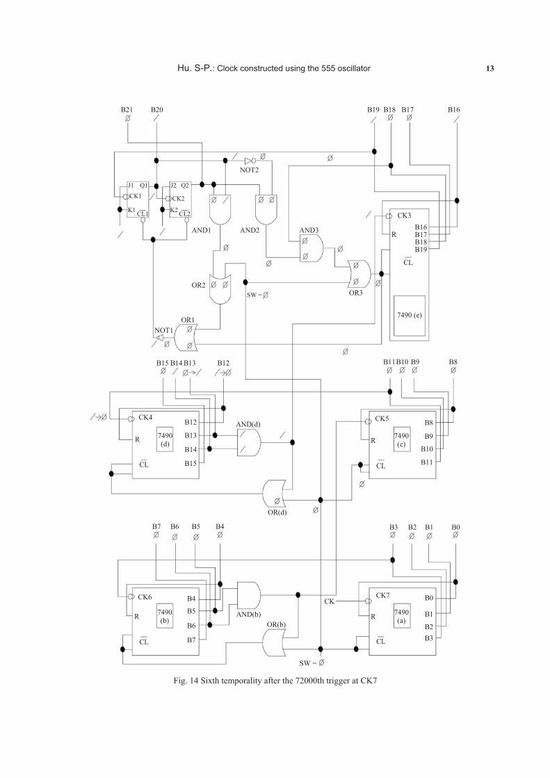
72000th trigger at CK7 is shown in Fig. 14. Because
CK4: / → Ø (negative edge trigger), it carries
7490(d) forward, that is B13 : Ø → / and B12: / →
Ø. Therefore, the output of the AND (d) gate is turned
to a / (high potential). The LED display denotes
19:60:00.
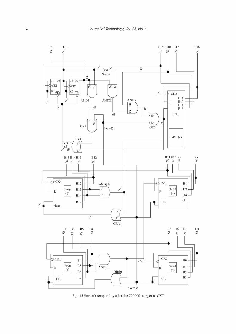
9. SW = Ø (grounding). The seventh temporality after
the 72000th trigger at CK7 is shown in Fig. 15. Since
the output of the AND (d) gate is / (high potential),
therefore the output of the OR (d) gate is also / (high
potential), 7490 (d) is cleaned and CK3 is also con-
verted to / (high potential). The LED display denotes
19 : 60 : 00.
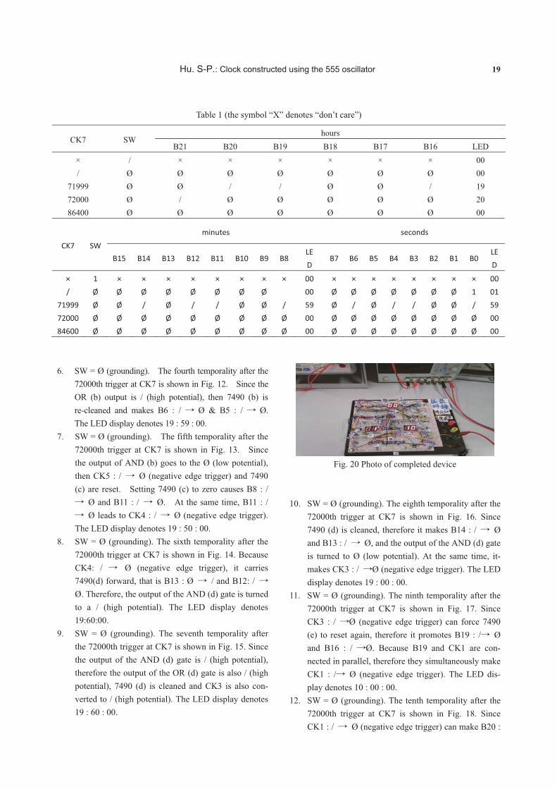
Fig. 20 Photo of completed device
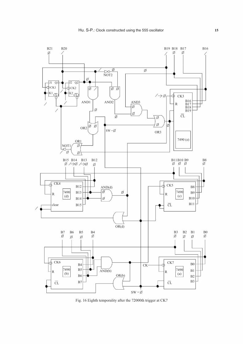
10. SW = Ø (grounding). The eighth temporality after the
72000th trigger at CK7 is shown in Fig. 16. Since
7490 (d) is cleaned, therefore it makes B14 : / → Ø
and B13 : / → Ø, and the output of the AND (d) gate
is turned to Ø (low potential). At the same time, it-
makes CK3 : / →Ø (negative edge trigger). The LED
display denotes 19 : 00 : 00.
11. SW = Ø (grounding). The ninth temporality after the
72000th trigger at CK7 is shown in Fig. 17. Since
CK3 : / →Ø (negative edge trigger) can force 7490
(e) to reset again, therefore it promotes B19 : /→ Ø
and B16 : / →Ø. Because B19 and CK1 are con-
nected in parallel, therefore they simultaneously make
CK1 : /→ Ø (negative edge trigger). The LED dis-
play denotes 10 : 00 : 00.
12. SW = Ø (grounding). The tenth temporality after the
72000th trigger at CK7 is shown in Fig. 18. Since
CK1 : / → Ø (negative edge trigger) can make B20 :

20 Journal of Technology, Vol. 35, No. 1
/ → Ø, therefore it promotes CK2 : / →Ø (negative
edge trigger). The LED display denotes 00 : 00 : 00.
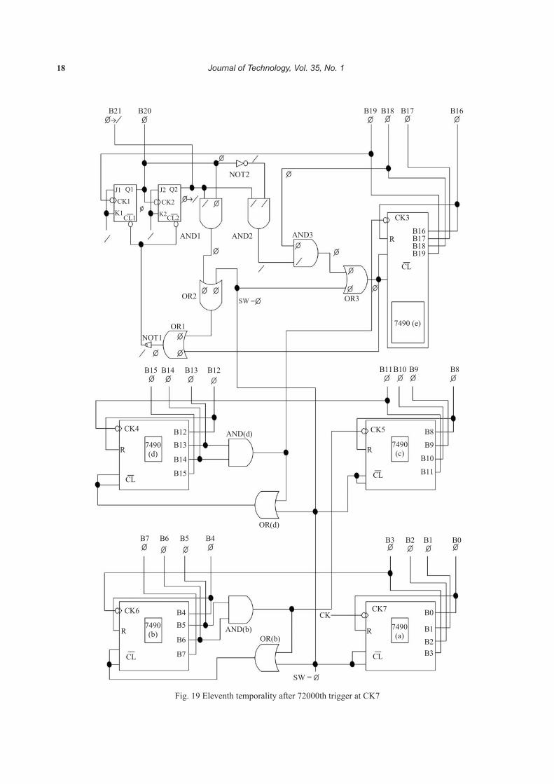
13. SW = Ø (grounding). The eleventh temporality after
the 72000th trigger at CK7 is shown in Fig. 19. Since
Q2 : Ø → / can make B21 : Ø → / , therefore it
causes the LED display to denote the time as 20 : 00 :
00.
14. Test Results is shown as Table 1.
15. The photo of completed device is shown as Fig. 20
V. CONCLUSIONS
1. In the first stage of the 555 astable multistage oscilla-
tor presented in this paper, only the first half of the
clock (charging clock) is transient, as shown in Fig. 3.
The time required for the first half clock (charging
clock) cannot be calculated, so it is not studied further.
The oscillator is stable after the first discharge (taking
time t1 (sec)) and after the second charge (taking time
t2 (sec)), as shown in Fig. 6. Thus, the output pulse of
the 555 astable multistage oscillator is the output
pulse of the transistor -transistor logic (TTL) circuit.
2. In order to ensure that the frequency of the 555 oscil-
lator pulse wave exactly matches the clock frequency
f = 1 (Hz), the charging and discharging resistance are
specially designed. On the charging route, we let the
resistance RA = RA1 + RA2 = 7.2K� and the capacitor
C = 100 μF, so that the time required for charging
becomes t2 = 0.5 (sec), as shown in Fig. 5. Similarly,
on the discharging route, we let the resistance RB =
RB1 + RB2 = 7.2K� and the capacitor C = 100μF, so
that the time required for discharging becomes t1 =
0.5(sec), as shown in Fig. 4. Looking at the overall
oscillator pulse wave, the full cycle T = t1 + t2 = 0.5 +
0.5 = 1(sec), the overall frequency
1 11( );
1f HZ
T� � � duty cycle
1 2 0.5100% 100% 100% 50%.
1
t tT T
� � � � � � � �
3. In this design, the logic IC7408 (AND gate) acts as a
hexadecimal, which is connected behind the IC7490.
The most significant bit (MSB) and the least signifi-
cant bit (LSB) of the BCD code output from the
IC7490 are removed. In other words, the BCD code
output by the IC7490 is taken from the middle two
codes.
23 22 21 20
MSB LSB
cancel retain retain cancel
= 22 + 21 = 4 +2 = 6
In this way, we can obtain the hexadecimal action.
4. In this design, when SW (switch) =/ (high potential),
then all IC7490 can be cleaned by IC7432 (OR gate)..
REFERENCES
1. Thomas, L. F. 2010. Electronic Devices (Conventional Current Version). 8th Ed. Taiwan: Chuan Hwa.
2. Chuan Hwa Book. 2001. TTL/IC Exchange Table of the world. 1st Ed. Taiwan; Chuan Hwa book.
3. Chang, Z. N. 2008. Digital Logic Design Laboratory. 1st
Ed. Taiwan: Tiked Books.
4. Cai, Z. Y. 2004. “Research and Analysis about
Low-Power Phase Noise CMOS Complementary LC
Resonant Voltage Controlled Oscillator.” Master’s disser-
tation, National Yunlin University of Science and Tech-
nology.
5. Lin, J. C. 2004. “The Research and Design of
Low-Voltage Wide-Range Adjustment Voltage-Controlled
Oscillators and Negative Resistance Voltage-Controlled
Oscillator.” Master’s dissertation, National Taiwan Uni-
versity of Science and Technology.
6. Huang, J. A. 2009. “The Design of Low-Power LC Volt-
age Controlled Oscillators Using Substrate Bias and Qual-
ity Factor Improvement Techniques.” Master’s disserta-
tion, National Yunlin University of Science and Technol-
ogy.
7. Chang X. H. (2011), “The Use of Clock Gate Replication
Technology to Construct a Clock Tree.” Master’s disserta-
tion, Chung Yuan Christian University.
Manuscript Received: Jan. 08, 2018
First Revision Received: Jun. 05, 2019 Second Revision Received: Aug. 19, 2019
and Accepted: Sep. 16, 2019


![Example 12.18 Analyzing Classical Form first movement, 26–47 · Allegro 1 2 G [Transition] 555555!5 555 55555555 555!555544 0 5 5555!5555 3 3 3 G 555555!5 555 5 555 5 555 5 555](https://static.fdocuments.in/doc/165x107/5eb9b97f2a57427eb12edee5/example-1218-analyzing-classical-form-irst-movement-26a47-allegro-1-2-g-transition.jpg)