CLEARINGHOUSE SCIENTIFIC AND TECHNICAL
96
CLEARINGHOUSE FOR FEDERAL SCIENTIFIC AND TECHNICAL INFORMATION CFSTI DOCUMEN- MANAGEMENT BRANCH 410.11 LIMITATIONS IN REPRODUCTION QUALITY / ACCESSION / - Q i. WE REGRET THAT LEGIBILITY OF THIS DOCUMENT IS IN PART UNSATISFACTORY. REPRODUCTION HA: BEEN MADE FROM BEST AVAILABLE COPY. Q 2. A PORTION OF THE ORIOIfAL DOCUMENT COHTAINS FINE DETAIL WHICH MAY MAKE READIN4G OF PHOTOCOPY DIFFICULT. O 3. THE 00idAL DOCUMENT CONTAIIIS COLOR, BUT DISTRIBUTION COPIES ARE AVAILA BLE IN BLACK-ANf-WIHITE REPRODUCTION ONLY. 4. THE INITIAL DISTRIBUTION COPIES CONTAIN COLOR WHICH WILL BE SHOWN iN BLACK-AND-WHITE WHEN IT IS NECESSARY TO REPRINT. Q 5. LIMITED SUPPLY ON HAND: WHEN EXHAUSTED, DOCUMENT WILL BE AVAILABLE IN MICROFICHE ONLY. O 6, LIMITED SUPPLY ON HAND: WHEN EXHAUSTED DOCUMENT WILL NOT BE AVAILABLE. O 1. DOCUMENT IS AVAILABLE IN MICROFICHE ONL\,. 8. DOCUMENT AVAILABLE ON LOAN FROM CFSTI ( TT DOCUMENTS ONLY). NBS 9 64 PROCESSOR:/, /. 7
Transcript of CLEARINGHOUSE SCIENTIFIC AND TECHNICAL

CLEARINGHOUSE FOR FEDERAL SCIENTIFIC AND TECHNICAL INFORMATION CFSTIDOCUMEN- MANAGEMENT BRANCH 410.11
LIMITATIONS IN REPRODUCTION QUALITY
/ACCESSION / -
Q i. WE REGRET THAT LEGIBILITY OF THIS DOCUMENT IS IN PARTUNSATISFACTORY. REPRODUCTION HA: BEEN MADE FROM BESTAVAILABLE COPY.
Q 2. A PORTION OF THE ORIOIfAL DOCUMENT COHTAINS FINE DETAILWHICH MAY MAKE READIN4G OF PHOTOCOPY DIFFICULT.
O 3. THE 00idAL DOCUMENT CONTAIIIS COLOR, BUT DISTRIBUTIONCOPIES ARE AVAILA BLE IN BLACK-ANf-WIHITE REPRODUCTIONONLY.
4. THE INITIAL DISTRIBUTION COPIES CONTAIN COLOR WHICH WILLBE SHOWN iN BLACK-AND-WHITE WHEN IT IS NECESSARY TOREPRINT.
Q 5. LIMITED SUPPLY ON HAND: WHEN EXHAUSTED, DOCUMENT WILLBE AVAILABLE IN MICROFICHE ONLY.
O 6, LIMITED SUPPLY ON HAND: WHEN EXHAUSTED DOCUMENT WILLNOT BE AVAILABLE.
O 1. DOCUMENT IS AVAILABLE IN MICROFICHE ONL\,.
8. DOCUMENT AVAILABLE ON LOAN FROM CFSTI ( TT DOCUMENTS ONLY).
NBS 9 64 PROCESSOR:/, /.7

i:AL P-ROGRIESS hEP"ORT
1 JanuarT 10,62 t 1 NX&lr 196L4
-~HIGH POWEF-R SEMICO1TeDUCTOR
PHASE SHIFTIN~G DEVICES
u oiY r, C ta c N0b s r 8 4 291
71 -oject Serial ~ R C3-3
Task 9637',
ZayDeparcin-, :. reau of S fps
-~ ~ -Electro-i'is Division
MICROWNNAVE
AkjSCCATS
INC.

FINAL PROGRESS REPORT
1 JANUARY 1962 to 1 May 1964
HIGH -POWER SEFJCONDUCTOR PHASE SHIFTING DEVICES
Contract NObsr-87291
Project Serial No. SR 008-03-02, Task 9637
Navy Department, Bureau of Ships, Electronics Division
This contract constitutes a direct extension of the work done onContract NObsr-81470, entitled "Phase Shifter Study (Non-Ferrite)",which terminated with the Sixth Quarterly Progress Report.
Prepared by:teph F. WhiteProject Manager
Approved by: Z14,-
Division ManagerSolid-State Circuits Division
May, 1964
MICROWAVE ASSOCIATES, INC.BURLINGTON, MASSACHUSETTS

~I-1
TABLE OF CONTENTS
I
A. Table of Contents I-1
B. List of Illustrations 1-4
C. Abstract 1-7
D. Purpose 1-8
E. Identification of Personnel 1-9
II Introduction II-1
A. High Power Phase Shifting II-1
B. Low Power Phase Shifting i1-3
IiI The Transmission Reflection Mode III-1
A. Circuit Configuration III-1
1. Matched Transmission Requirements III-2
2. Controlled Reflection Terminations 111-5
a) Continuous 111-5
b) Step 111-5
B. Circuit Implementation III-l)
1. Continuous Type III-10
a) Analytical Procedure III-10
b) L-Band Model III-10
c) S-Band Model 111-16
d) RF Power Limit ITI-19
e) Temperature Effects 111-21

1-2
TABLE OF CONTENTS
cont.) Page o.
III B. 2. Step Type 111-21
a) General Comments ITT-21
b) L-Band Model iIi-24
c) S-Band Model 111-29
d) B Power Limits 111-33
IV The Transmission Mode IV-1
A. Design Considerations IV-1
1. Introductory Remarks IV-1
2. Phase Shift and Transmission Match IV-1
a) Equivalent Line IV-1
b) Maximum VSWR IV-i
c) Phase Shift Approximation IV-4
d) Exact Solution for Cascade Circuit IV-6
e) Approximate Loss Expressions IV-6
B. Circuit Implementation IV-9
1. L-Band Circuit IV-9
a) Stub Approach IV-9
b) Measured Characteristics IV-11
c) Peak Power Limits IV-15
d) Variation of Phase Shift with Frequency IV-18

1-3
TABLE OF CONTENTS
(con't.) Page No.
IV B 2. S-Band Circuit IV-20
a) LC Circuit Approach IV-20
b) Variation of Phase Shift with IV-28Frequency
c) Measured Characteristics IV-28
d) Peak Power Limits IV-36
V Conclusions V-1
VI Bibliography VI-1
Distribution List

1-4
I B. LIST OF ILLUSTRATIONS
FIGURE SECTION CAPTION
1 III-A-I Transmission-Reflection Phase Shifters
2 III-A-I Reflectively Terminated Hybrid Coupler Equations
3 IIi-A-I Theoretical VSWR. versus Frequency Character-istic of a Refleffively Terminated Hybrid Coupler
4 III-A-I Measured and Calculated VSWR. of Symmetric OpenCircuit Terminated Hybrid Coupler
5 III-A-2 Controlled Reflection Terminations
6 III-A-2 Continuously Phase Variable Single VaractorT" rmination
7 III-A-2 Continuously Phase Variable, Two VaractorTernitnation
8 III-B-l-a Varactor Termination Parameters
9 III-B-l-a Varactor Termination Admittance Plot
10 III-B-l-b Measured and Calculated Values of ContinuousPhase Shift
11 III-B-i-b Measured Values of Phase Shifter Insertion Loss
12 III-B-i-b Phase Shift and Insertion Loss of L-Band PhaseShifter
13 III-B-l-c Phase Shift and Insertion Loss of S-Band PhaseShifter
14 III-B-l-d Effect of Increasing RF Power in a ContinuousPhase Shifter
15 III-B-l-e Phase Shift versus Bias with Temperature asParameter
16 III-B-2-a The Transmission Reflection Phase Shifter
17 III-B-2-a Phase Shift versus Peak Power

LIST OF ILLUSTRATIONS
(con't.)
FIGURE SECTION CAPTION
18 III-B-2-a 4-Bit Phase Shift versus Bias
19 III-B-2-a Insertion Loss and VSWR
20 III-B-2-c S-Band Step Phase Shifter Equivalent Circuit
21 III-B-2-c Step Phase Shifter Phase Shift
22 III-B-2-c Step Phase Shifter Insertion Loss
23 IV-A-1 & Transmission Phase ShifterIV-A-2-c
24 IV-A-1 Geometric Description of Phase Shift Approxi-mation
25 IV-A-2-a Equivalent Line Length Approximation
26 IV-A-2-d Exact Gain Expression for Transmission PhaseShifter Cascade
27 IV-B-1-a L-Band Transmission Phase Shifter Prototype
28 IV-B-1-b Photograph of L-Band Transmission Phase Shifter
29 IV-B-1-b Measured Phase Shift of L-Band Model
30 IV-B-1-b Measured Insertion Loss of L-Band Model
31 IV-B-1-c Phase Shift versus Peak Power Obtained withTransmission Circuit Using Two 800 Volt Switch-ing Diodes
32 IV-B-l-d Calculated and Measured Phase Shift versusFrequency
33 IV-B-2-a PIN Diode Equivalent Circuit
34 IV-B-2-a Equivalent Circuit, with Loss, of IterativelyIV-B-2-d Loaded Line Phase Shifter Prototype Network
35 IV-B-2-b Susceptance versus Frequency Diagram
I -

I-o
LIST OF ILLUSTRATIONS
(con't.)
FIGURE SECTION CAPTION
36 IV-B-2-c Photogr&ph of Two Section Transmission PhaseShifter
37 IV-B-2-c Phase Shift Characteristic of Two SectionPhase Shifter
38 IV-B-2-b insertion Loss Characteristic of Two SectionTransmissicn Phase Shifter
39 IV-B-2-b VSWR Characteristic of Two Section TransmissionPhase Shifter
40 IV-B-2-b Photograph of S-Band Transmission Phase Shifter
41 IV-B-2-b Performance of S-Band, 8 Section Iterative
Phase Shifter with Diodes Removed
42 IV-B-2-b S-Band Transmission Phase Shifter 'erformance

1-7
i C. A_ STh. CTT-
T= -report s u-rizes the efforts -b "_-" s. e- s to
investigate semiconductor phase shifting te i. iques in :he L ar.d S- fre-
quency bands. The summar7 descr.-hee analysps and xper-mm ent-9! stdies
of two basic phase shifter cir:uit modes, tae tra is-ion phase hiftei
and the transmission-ref!ection vhsse shifter. in the Et-,er , -th
continuous and discrete increment phase control ,aels ae treated.
Highest power an, lowest insertion tozs resiults were btainel
using the transmission zcode ehan.cing its usaeflness in phased array
radar. T' -' :io7ep: u!fa! !r- rt a
LIr-xd Slinds with total insertion loss values O.'
- 4- ned s -re-pectively for l80 , 8 equal inrezent ikh h~ft
ie-~- ~e eri~wiht Iw~s It
The transmission re'l-ection circuit mode utilizing PIN diodes
for phase control basically yields switchable time delay, and models
were constructed which were operated to 4.8 kilowatts at L-band and 5
kilowatts at S-band.
Continuous phase control for low power applications was demon-
strated at L and S-bands with a figure of merit of approximately 250
degrees phase shift per decibel of insertion loss per kilo-megacycle of
operation using the transmission reflection mode. These used 180 Kmc
cut-off frequency varactors as phase control elements. ( ) ,

i-8
I D. PURPOSE
The purpose of this work is to investigate microwave phase
shifting techniques, excluding ferxoagnetic and mechanical methods, to
make recommendations for new phase shifting techniques which provide
improved electronic control, and to develop phase shifter models utiliz-
ing these techniques.

I-9
I E. IDENTIFICATION OF PERSONNEL
Name Title
J. White Project Manager
L. Yesler Semiconductor Engineer
R. Galvin Diode Characterization Engineer
H. Griffin Circuit Engineer
Dr. K. hbrtenson Consulting Physicist
Biographies of these personnel have been included in the
previous reports.

I!-i
II INTRODUCTION
A. High Power Phase Shifting
The desirability of radar systems having large RF power capa-
bility as well as rapid antenna pointing agility suggests the use of
phased array antenna techniques. Such phased array antennas require
precise RF phase control, and for this function various schemes have
been recommended and tried within the last few years.
These methods have included phase control at IF frequencies
and the deployment of frequency multiplying chains to obtain microwave
energy of controlled phase. Another technique consists of the use of
sections of waveguide with spaced apertures through which microwave
energy may escape by radiation; the direction of radiation may be con-
trolled by adjustment of the frequency of the microwave energy; this
technique makes use of the dispersive property of waveguide when opera-
ted in a transmission mode near cut-off. Using this technique, beam
steering can be accomplished at a rate that is limited only by that
rate at which the transmission frequency can be varied. However, in-
herent in this method is relatively narrow bandwidth operation; since
the direction the array antenna points is, by design, a function of
frequency.
Another form of phase control is effected by the construction
of an antenna having a multiplicity of RF input ports, each of which is
connected corporately to the total number of radiating elements in such
a way that the radiated beam points in a unique direction when fed at one

11-2
particular port. Beam scanning, then, is affected by switching the trans-
mission power from one port to another. In this case, a large number of
transmitter tubes is necessary unless the transmitter energy can be
switched between the various antenna input ports. Then the accomplish-
ment of super high power radars of this form is dependent upon success-
ful development of appropriate high speed, high power microwave switches.
The RF power capability of switches and microwave phase shifters
can be shown commensurate for typical applications. This suggests, then,
that antenna pointing might be affected in a more direct manner using
microwave phase shifters which are individual to separate antenna ele-
ments or groups of antenna elemcnts. Such microwave phase shifters take
the form of a two-port transmission network whose propagation constant
is conveniently controlled.
Recommended microwave phase control networks have included the
use of electro-mechanical and electro-hydraulic, ferrite, and semicon-
ductor elements. Though the salient features and disadvantages of each
are indeed unique, they vary distinctly by virtue of the speed at which
control can be effected.
Electro-mechanical or hydraulic devices typically have control
times of the order of milliseconds. The properties of ferrite materials
may be varied by the application of a magnetic field and such control
usually is accomplished in tens to hundreds of microseconds.
Semiconductor devices are inherently much faster in their res-
ponse since their properties can be varied with the application of a

11-3
bias current or voltage directly, and this control is easily effected
in one microsecond with switching times considerably below 100 nanoseconds
accomplishable under some circumstances.
High power phase shifting application is performed well by semi-
conductor PIN diodes which effect phase control through discrete switch-
ing from a low impedance at forward bias, typically less than 1 ohm of
resistance, to a high impedance at reverse bias, typically greater than
100 ohms of capacitive reactance in the L-band frequency range. Since
the control element essentially varies as an on-off device, variations-
in its impedance resulting from manufacturing reproducibility, changes
in temperature, or changes in applied RF power are usually insignificantly
small; and highly desirable distortion-free, reproducible operation can
be obtained.
B. Low Power Phase Shifting
Applications which require microwave phase control at low power
levels include countermeasure networks, driver stages in high power
parallel chain -amplifier circuits, and automatic, microwave impedance
measuring, bridge circuits. Within a countermeasure circuit, an enemy
signal may be phase modulated with random or deceptive information and
be transmitted to its original source. In this way, accurate target
velocity determination by interpretation of the return signal frequency
deviation or phase change can be inhibited.
Within a high power amplifier chain, a microwave phase shifter
may be used to control the phase of low level driver stages in order to

11-4
keep in synchronism the output of parallel microwave high p3wer tubes,
that are used in conjunction, for the generation of higher power than
can be obtained with single tubes. A further advantage of this con-
trolled phase, parallel tube, high power generation technique is that it
also can be used for switching the resultant microwave energy. Typically,
for example, this might be accomplished with two tubes by feeding their
output power into separate ports of a 900 hybrid coupler. The combined
energy can then be made to exit from either of the coupler's remaining
two ports according to the relative phase between the two input signals.
In an automatic, microwave impedance measuring, bridge circuit,
a phase shifter may be used to produce at high speed a calibrated phase
shift in the known impedance arm, permitting instantaneous measurement
of a rapidly varying unknown microwave impedance.
In these low power phase shift applications, semiconductor
varactor diodes may be used to yield large ranges of continuous phase
shift. In such circuits, the varactor impedance is essentially capaci-
tively reactive and varies in a continuous manner according to an applied
bias. If the applied microwave voltage is small compared to the bias,
then the diode impedance, and hence the phase shift obtained, is deter-
mined only by the bias voltage, and distortion-free operation is obtained.
Typically, in 50 ohm transmission systems, the RF level for distortion-
free operation is less than 1 watt, although operation to higher levels
may be extended where some change in the phase shift versus bias char-
acteristic with increasing power is not objectionable.

11-5
The advantage gained by using varactors when the RF power level
is low in the phase shift design is that wide phase shift ranges with
relatively few diodes may be adhieved. Single continuous phase shift-
ing devices have been built to yield about 2500 of phase shift per
decibel of insertion loss per kilo-megacycle of operating using 170 Kmc
cut-off diodes; as much as 270 of phase shift was obtained using two
varactor diodes, only one diode would be necessary if a circulator were
to replace the hybrid coupler used in the balanced circuit tested.
High power operation of continuous phase shifters was studied,
under Contract N0bsr-1470, using special varactor diodes having break-
down voltages exceeding 500 volts. However, the variation of phase
shift with operating RF power level was judged to be a serious restric-
tion on the ultimate usefulness of this continuous phase shifter form;
and, therefore, no further efforts were performed to operate at high
power with continuous type varactor diode phase shifters.

III1-i
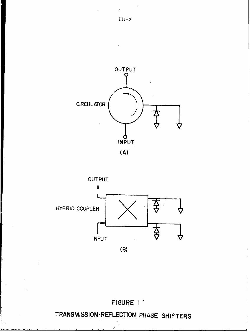
III TRANSMISSION-REFLECTION MODE
A. CIRCUIT CONFIGURATION
1. Matched Transmission Requirements
The transmisson-.reflection phase shifter circuit can be
made to have matched two-port characteristics that are independent of
its phase shift characteristics by employing the directive properties
of a circulator or hybrid coupler. Control of the phase difference
between input and output waves is effected, then, using terminations for
the directive circuit whose reflection coefficient has near unity magni-
tude but controllable phase. These circuits are depicted in Figure (1).
Use of the circulator approach yields a circuit whose phase shift is
non-reciprocable between input and output terminals. The hybrid coupler
circuit of Figure (1-b) requires a pair of symmetric controllaLle termi-
nations, but possesses reciprocal operation. In addition, the matched
transmission bandwidth of the hybrid coupler circuit can be achieved for
bandwidths of an octave or more.
Hybrid couplers with matched impedances at all ports have
been analyzed in detail by Cohn, Sherk, Shimizu, Jones, Bolljahn, Oliver
and many others. From these results, the reflection coefficient exper-
ienced at the input of a hybrid coupler symmetrically terminated with
reflection coefficients, 1, may be calculated as shown in Figure (2).
The maximum VSWRin resulting from symmetric, unity magni-
tude reflection cosfficients, 1, at the"3 db ports" is shown plotted in
2Figure (3) with the center frequency power coupling ratio, k , as para-
meter. Experimental versus theoretical performance of a 2.7 db hybrid
111-2
OUTPUT
CIRCULATOR
INPUT
(A)
OUTPUT
HYBRID COUPLER
INPUT
(B)
FIGURE I
TRANSMISSION-REFLECTION PHASE SHIFTERS

Zoe,Zoo
2 0 Zoo= odd mode impedance
zo Zoos- even mode inpedonce
Zo0 Zoe ZooZozI (normalized)
It Zoo - Zoo
SCATTERING EQUATION: b= so
0 f 0 f2
S ,=fl 0 f 2 0
0 f2 0 ft
f2 0 fl1 0
jk sin o
flf --'- ~ 0+ i
=_-___ k__
VI-k 2 COS + j sine.
-i/I-k2
Scose + j sin -
=I-k 2 (sin2 . I) I
R i n _ + Irinis- _ Iti
FIGURE 2
REFLECTIVELY TERMINATED HYBRID COUPLER EQUATIONS

1 4
40D
3.6-
3.4
2k2- 40 db,--3.6 db--
2,B--303 k'-4Odb
~-2B26- -2.db
>241
22
1.6-
1.2
4 .5 .6 .7 .8 .9 1,0 11 LZ L3 1 4 15 LS 17
NORMALIZED FREQUENCY(AT f a.0 - /)
FW.RE 3
THEORETICAL VSWR In VERSUS FREQUENCY CHARACTERISTICOF A REFLEMTEMJY TERMINATED HYBRID COIPLER

!ii-5
coupler so terminated by sy=metric open circuits is shown in Figure (L).
2. Controlled Reflection Terminations
Either continuous or discrete increment control of the
termination reflection coefficient may be effected accordingly as varac-
tor or Fil diodes are used as control elements in the termination, Fig. 5. In
Figure (6) is eh-cwn the relative change of reflection coefficient phase
as a function cf the normalized variable capacitive susceptance, B, of
a continuously controlled termination with the short circuited termina-
tine line length as parameter. A termination using two varactor diodes
together with its phase shift versus normalized capacitive susceptance
characteristic is shown in Figure (7). More than 3600 of phase shift
in principle is obtainable from this circuit. Experimental results were
obtained for the single diode termination and are described in the next
section.
Although continuous phase shift is '.ractive, its imple-
mentation with varactor diodes typically is limited to very low power
levels, of the order of milliwatts. This occurs because the capacity
of the varactor is a function of the instantaneous voltage applied to
it. Thus, tc prevent distortion of the phase shift versus bias charac-
terist:c as well as attendant harmonic generation, the RF voltage applied
must be very zmmsll compared to the control bias voltage. For this reason,
the discrete increment phase shifter using a PIN switching diode is desir-
able for linear high power operation, In this case, depicted as Figure
(5-b), the pba-e shift ie equal approximate.y to twice the length of

2.9-
2.8"
2.7- 0
Z61
2.5Q
24-
23-
2.2- 0
2.1-
0 0
L
I.6-15 0
1 .5-0
14-
0 00- 0
I.0
500 8oo 1000 1200 1400 1600 IWO 2000 2200
FREQUENCY-(mc)fo 1350
FIGURE 4
MEASURED AND CALCULATED VSWR IN SYMMETRIC OPEN CRU TERMINATED HYBRIDcX3UPLER

0-~
jB YozI
(A) N€RACTOR DIODE TERMINATION EQUIVALENT CIRCUIT
rin
> Yo =1
0-
(B) PIN DIODE TERMINATION EQUIVALENT CIRCUIT
FIGURE 5
CONTROLLED REFLECTION TE TINAT1ONS

*0)
04
(00
0~~ 0 VTCD CID c2

oz om(YOD f- o W) VD W) CQ N
0
0T0N
w31w
00 00, >
w cr wL
00Cl
D:
'4:

III-10
short circuited line switched and, in principle, has a magnitude pro-
portional to frequency if a nondispersive line length, e is used.
B. CIRCUIT fMPLEIENTATION
1. The Continuous Phase Shifter
a. Analytical Procedure: The circuit and phase shift
characteristics shown in Figure (6) are useful for selection of approxi-
mate circuit parameter values, but a more complete equivalent circuit
which includes the diode resistance and parasitic series inductance is
necessary for accurate calculation of the terminatiods phase shift and
insertion loss. The parameters of an experimental varactor termination
are shown in Figure (8) and the resulting admittance plot of the termi-
nation is shown in Figure (9) for an operating frequency of 1,000 mc.
At this frequency, the diode package capacity, approximately 0.3 pf, has
been lumped into the total diode capacity, C. A plot of C versus applied
bias voltage for both of the diodes used in the symmetric termination
pair is also included in Figure (8).
b. L-Band Model: A pair of terminations whose calculated
admittance versus control bias for the included varactor diode is shown
in Figure (9), was used at the output of a 3 db hybrid coupler and the
measured and calculated values of phase shift may be seen compared in
Figure (10). These agree closely at 1000 Mc with somewhat larger dis-
crepancies between measured and calculated phase shift versus bias char-
acteristics at the higher frequencies 1500 Mc and 2000 Mc. This may
have resulted because the length of the short circuit line used as a

111-11
100T" -
I0. j C
o 1.9nh
0- %.-Zo 50-[L
6.0-
0 IIII I I I1
0 10 20 30 40 50 60 70 80 90
REVERSE BIAS
FIGURE 8
VARACTOR TERMINATION FARAMETERS

rNATTEFIGURE 9 111-12 ___W.__0
S RATOR TERNATION-AIMITTANCE-P-WDT OG~o~75~W DATE
ISMITH CHART gotMNMICROWAVE ASSOCIATES BURLINGTON IMASS.
LADM ITTANCE COORDINATES
FREQUENCY =1000 mc
00
La 0
0 0
A0
.5,0
46.'~~0
~0 0~rob
1410 tOOCO 001- 0
Ot- 110
1-0 cro

'100,0 mc
- .. MEA3URED
90- // CALCULATED
160 -/_I.- -
1730- .t
160-
_ 50- 101.0LJ 140-
50-
0
Ij10-
110 00
> 90 7
80
7000
40 / FIGURE 10
30 / MEASURED AN~D CALCLLAT7ED VAWES
30 /OF CONTINU2GS PHASE SHIFT
20
10
10 20 30 40 50 60 70 8090BIAS (VL~

!I-1Z
back-up for the shunt mounted diode is known only approximately. A
spring finger sliding short circuit hbd been use,. to terminate the line
and the exact location of the short circuit, as well as the characteristic
impedance of the line in the vicinity of the short circuit fingers, are
lonv only approximately,
The insertion lose of the continuous phase shifter over
the L-ba d frequency range is shown plotted in Figure (1l). In all cases
examined, the frequancy for which the maximum phase shift rasulted was
also that at vlich the maximum insertion loss was obtained. In this case,
the maximum loss measured at 1000 Mc was 2.1 decibels. The measured phaseshift was about 2400. Considering that the circuit losses with diodes
removed were of the order of 0.3 decibels, the figure of merit for the
diodes as used in this configuration was approximately 1350 of phase shift
per decibel of insertion loss.
More phase shift per decibel of insertion loss would be
expected from diodes with higher cut-off frequencies. The results just
described were achieved with diodes whose cut-off frequency measured at
the 90 volt breakdown voltage was 41 Kmc. This is calculated using the
series resistance value 2.6 ohms and the voltage breakdown capacity of
1.5 picofarads. Within the last quarter, higher cut-off frequency diodes
were used in an L-band phase shifter circuit. Measurements were made at
1800 Mc since the input VSWR to this particular coupler was minimal at
this frequency.
The measured phase shift and insertion loss may be seen

2- FREQ. 1200mc (0)
0 (A)
1z I.O-0
0
0 20 40 60 80 90
REVERSE BIAS VOLTAGE
FIGURE I1
INSERTION LOSS VERSUS BIASOF CONTINUOUS PHASE SHIFTER

111-16
plotted in Figure (12). A maximum of 1840 of phase shift was obtained
while the maximum insertion loss did not exceed 1.1. f, again, 0.3 db
is subtracted to account for the circuit losses, the figure of merit for
this phase shifter was about 230 of phase shift per decibel of insertion
loss. This was also achieved at a higher operating frequency, 1800 Mc,
compared with the previous 1000 Mc. If the figure of merit is made pro-
portional to the operating frequency, then these results yield about
4150 of phase shift per decibel of insertion loss per kilo-megacycle.
The diodes used had a capacity variation of 4.5 picofarads at zero bias
to 0.9 picofarads at breakdown, 60 volts. The series resistance was very
nearly 1 ohm and, thus, the cut-off frequency of these diodes was about
175 Kmc. From these results, it can be seen that the phase shifter
figure of merit was nearly proportional to the cut-off frequency of the
diodes used.
c. S-Band Model: Also within the last quarter, an S-band
continuous phase shifter -was constructed and tested at 2800 Mc using the
same 5 picofarad diode pair quoted for the 1800 Mc performance. The
results obtained may be seen in Figure (13). 1900 of phase shift was
achieved with a maximum insertion loss of 1.4. Again, if about 0.3 deci-
bels of loss are attributable to the circuit, then the phase shifter fig-
ure of merit is about 485 phase shift per decibel of insertion loss per
kilo-megacycle. Considering that the insertion loss allowance for the
circuit with diodes removed may not in all cases be the same, these re-
sults are in fairly close agreement. A figure of merit may be then

FREQUENCY: 1800mG
200PHSSHF
160
w 120
1.~
40 AINSERTIN LOSS .6
z
30 4050 60
0 10 REVERSE BIAS \tOLTAGE
FIGURE 1*2
PHASE SH-lFT AND INSERTION LOSS OF
L-BAND PHASE SHIFTER

fil- 1p
FREQUENCY 2800 m
200-
160-
W 120
cn 80-2
~ INSERTION LOSS
40-o 1.0
00
0 10 20 30 40 50 60REVERSE BJAS VOLTAGE
FIGL'9E 13
PHASE SHIFT AND INSERTKJN LOSS OFS-BAND PHASE SHwIFTER

111-19
defined for continuous phase shifters in the L and S frequency bands
which use varactor diodes having capacity values in the 1 - 10 picofarad
range and are adjusted to yield phase shift increments of about 2000.
This indicates that the empiric relationship of Figure (5) can be used
with good approximation to estimate the inter-related phase shift, inser-
tion loss, operating frequency, and diode figure of merit -- the cut-off
frequency.
F. (Degrees) (Diode Cut-off FreQuency)I.L. (Decibel) (Operating Frequency)
Equation (1)
d. RF Power Limitations: The continuous phase shifter
using varactor diodes is limited to low RF power levels. The first
limiting factor is the variation of the diode capacity with the applied
RF voltage. This is very undesirable because at RF power levels appre-
ciably larger than 1 watt, the phase shift versus bias characteristic
becomes a function of the operating power. This result may be seen
plotted in Figure (14); it was first discussed in the Second Quarterly
Progress Report. Even if this distortion of the phase shift character-
istic is tolerable, the effect of diode rectification inhibits operation
of the phase shifter beyond RF levels of about 25 watts. These RF power
ratings are based upon a 50 ohm hybrid coupler transmission reflection
continuous phase shifter using diodes with reverse breakdown voltages
of approximately 100 volts. This nonlinear behaviour results from the
varactor diode's ability to maintain a capacity determined by the applied

90-
80- O.Imw
5w PK
70-
w
.40-
30'
I0-
10
10 20 30 40 50 60 70 80BIAS VOLTAGE
-10 FIGURE 14
CONTINUOUS PHASE SHIFTER4 PARALLEL MOUNT DIODES

111-21
voltage at its terminal even when this voltage varies at a microwave
rate. A means for Slowing down this response -- and thus a means for
insuring circuit linearity with RF power -- results from the use of an
intrinsic semiconductor region between the P and N regions. The result-
ing "PIN Diode", as will be seen, is suitable for operation at tens to
hundreds of kilowatts of RF power.
e. Temperature Effects: The varactor diode capacity is
not a sensitive function of temperature and, therefore, it might be
expected that very little phase shift variation would occur as a function
of ambient temperature for the phase shifter models described. Experiment-
al verification may be seen in Figure (15). An L-band phase shifter which
yielded 1850 of phase shift at an ambient temperature of 300C. was meas-
ured to have 1890 of phase shift at 800C. Thus, less than a 2% variation
of phase shift occurred over a 500C. temperature excursion. A portion of
this phase shift variation might be expected merely from the expansion
from the circuit parts. particularly the short circuit line length located
behind each diode. This essentially invariant characteristic of phase
shift with temperature for the continuous phase shifter typifies and is
a perticularly salient feature of microwave semiconductor control devices.
2. The Step Phase Shifter
a. Analytic Procedure: Calculation of the phase shift to
be expected from the hybrid coupler terminated with PIN diode switched
reflections is obtained straightforwardly by considering the equivalent
circuit shown in Figure (5-b). In the models to be discussed, PIN diodes

I11-".
FREQUENCY = I300mc
180" 800 C =TEMPER
140-
120-
)
60-
40-
20-
0 K) 20 30 40 50 60 70 80 90
REVERSE BIAS VOLlA3E
FIGURE 15
PHASE SHIFT VS BIAS WITHTEMPERATURE AS PARAMETER

111-23
were used whose junction impedance was approximately 0.5 ohms of resis-
tance when measured at 1000 Mc and forward biased with approximately
100 milliamperes of current. When reverse biased with -100 volts of DC
bias, the RF impedance was essentially that resulting from the series
combination of a 1 to 2 ohm resistance in series with about 0.8 pico-
farads of capacity. In all L-band models, this impedance variation was
assumed to be very nearly a short. or an open circuit accordingly as the
diode was forward or reverse biased.
In addition to these impedance values, approximately
1 nanohenry of series inductance results in a typical diode mounting
circuit. This may be attributed both to the inherent series inductance
of the diode package as well as any contributions made by the circuit in
which the diode is used. In all cases, this series inductance was reso-
nantly tuned by means of a capacitor, for example, approximately 25
picofarads of capacity will series resonate 1 nanohenry of inductance
at 1 kilo-megacycle. The resulting bandwidth over which this tuning
was useful typically exceeds 10% to 20% in a 50 ohm characteristic im--
pedance transmission line circuit.
The phase shift of the terminations shown in Figure
(5-b), then, is approximately equal to twice the length of short cir--
cuited line following the diode. This is considered a true time delay
phase control component, and this feature is particularly desirable for
use in broadband phased array antennas. In practice, phase shift pro-
portional to frequency is achieved only approximately. Several factors

111-24
tend to inhibit the achievement of this linear phase shift versus fre-
quency characteristic. First, the diode does not switch between a short
and open circuit but rather between a reactance which may be made zero
only at a center frequency by resonant tuning and a line shunting sus-
ceptance which, again, may be made zero only at a single frequency by
the use of parallel resonant tuning.
Second, the shortest length achievable for e is limited
by the proximity with which a short circuit may be placed with respect
to the line shunting diode. On the other hand, long lengths for the
value e also are undesirable because they become significantly lossy.
In addition, if the line length, e, is long, then small variation in fre-
quency produces a rapid variation of the shunt susceptance placed in
parallel with the diode. Under forward bias conditions, a match condi-
tion may be achieved in which the diode's resistance, however small, may
be transformed to a value near to the transmission line impedance with
the result that very high insertion loss is obtained together with high
energy dissipation in the controlling diode.
In this study, only the peak power handling capability
achievable for phase shifters having phase shift value of 1800 or less
was examined.
b. L-Band Model: The equivalent circuit of the L-band
model of the transmission reflection phase shifter may be seen in Fig -
ure (16). Assuming the diode to vary between short and open circuit
impedances, the phase shift obtained is equal to e, twice the length

III-25
SYMMETRIC TERMINATIONS
'" , u !- - - - -- --,
j I A ,
- k - -"RF INRIF OUT 3db I
HYBRID COUPLER
a) TRANSMISSION -REFLECTION PHASE SHIFTER
FORWARD BIAS REVERSE BIAS
8/2
JCIRCUIT AND DIODEPACKAGE INDUCTANCE
Zo Ls Zo
oDIODE FORWARD DIODE REVERSERs '4RE3ISTANCE R's RESISTANCE
DIODE REVERSEjTO C CAFACITY
LAS DC BLOCKINGCs CAPACITOR
b) EQUIVALENT CIRCUITS OF DIODE TERMINATION
TRANSMISSION REFLECTION PROTOTYPEFIGURE 16

111-26
of short circuit line used in the termination. The voltage applied
across the reverse biased diode is then approximately equal to 2VLsin(e/2).
Thus, the power handling capability for the phase shifter will be related
to the maximum voltage applicable to the reverse biased diode according
to Equation (2). 2
oM- 2Z° sin2 (8/2) Equation (2)
A pair of 800 volt breakdown PIN diodes was used to
vtrify this expression. Since the maximum voltage for a given power
level nust be sustained by the diodes in a 1800 phase shifter, the power
level which the diodes susta-ined while drawing a reverse leakage 3urrer'.
of about 5 microamperes each -'- from which iminent breakdo-n could be
expected -- was taken to be equal to P The increase in power handling
capability resulting b reducing the phase shift was then measured and
compared with that which would be expected using Equation t2). These
results are shovn compared in Figure (17). A maximum peak power of 48
kilowatts was achieved with an RF pulse length of 5 microseconds and a
duty cycle of .001 at 1300 Mc. The phase shift obtained was approxi-
mately 21.50 and the insertion loss was 0.6 decibels.
Using similar circuits, a cascade 4 bit phase shifter
was constructed, that is, the phase shift achieved in the respective
sections was 0- 1800 , 0 - 900 , 0 -45 0 , and 0 to 22o. In Figure (18),
the measured versus theoruticsl phase shift versus bias condition my be
This work was not perfo-zed under this contra,-t but the results areincludel here for completeness.

Ci~~~ -C N O21- 27)S-T
4 --
* ..- I-- -. - * -
* - ~0
*c 0
~ .4
.;. :: ~VI
-. I H 4-
000 0* -. CD -
7tTJq-blX'A3~ -- .!*
POE OF STEPL__EFTE
FIUR 17

360-
p
315-/
I
270-
I
//
//
//225- MESUE
f10 V
1 THEORETICAL
180.T 9HS1HFERV.BA
Lif
135 A/ FREQUENCY= 1300m
90-/( ~*
45-%
o/
0 4 8 12 16BIAS SIATE
FIGURE 18
4- BIT PHASE SHIFTER VS. BIAS

111-29
seen. Fifteen values of phase shift may be obtained with a 4 bit cascade,
00
the 00 and 360° state are considered equivalent. The maximum departure
from the theoretical linear phase shift versus bias state slope was 30.
The input VSWR to the cascade and the total insertion
loss are shown in Figure (19). The maximum input VSWR was 1.4 and the
mean value was 1.2. The maximum insertion loss was 1.3 decibels and the
mean value was 1.6 decibels. Since diodes having approximately 800 V
reverse breakdown were used, the voltage limited peak power capability
of this cascade was approximately 2 kilowatts.
c. S-Band Model: A transmission reflection type S-band
phase shifter was constructed. The circuit configuration, together with
pertinent characteristics of the diodes used, may be seen in Figure (2C).
In this case, special high voltage PIN diodes were made. These con-
sisted of a three dje stack connected together internally in a single
Axial Pill package. The resulting phase shift and insertion loss meas-
urements made with the sliding short position as parameter n be seen
in Figures (21) and (22) respectiveiy. From these, it is seen that high
loss behaviour is incurrPA fnr *hrt positions between 0 and 1.25 inches.
This discrepancy occurs because the diodes' series reactance is most
likely not perfectly tu,,ed at the operating frequency and .he short cir-
cuit line length tends to match the diodes' resistance to the impedance
of the line, resulting in high loss and unvarying phase shift. This is
not a basic limitation for a multi-step phase shifter since the full
range of 0 - 1800 phase shift was achieved between 1.25 and 2.25 inches.

I I 1- 30
1.3- 0 LOSS .LUES
012 0 000 iMEAN LOSS 1.16dh
0 0 -0
0
1.0-
Cl)0 .6-
Z 41 0 SWR VALUES 0 -14
oo tMEAN SWR=L12
O2- - o - _-t-.2
0 0 o
00
0 90 !so 270PHASE SHIFT (M P.EGS
FIGURE 19

RF OUT
RF IN S-BANDSTRIPLINE 3db
HYBRID COUPLER
DIODES
DIODE #1 *2
TYPE PIN P11N
BREAKDOWN VOLTAGE 2000V 2400V
CAPACITY AT ZERO BIAS 158 PF 1.81 PF
RESISTANCE AT i0MG 7.01R 6.O&?I
AT 5OMa I.9&) 2OS
AT IoomG 1.4,Q .7
S BAND STEP PHASE SHIFTER
EQUIVALENT CIRCUIT
FIGURE 20

T :-,Z?
240 -- 21 , ,
I- i ss'r'i
O~%SAfFTtK220 ......- .R E N Y =_L30 I_
RF P -,OR Im nw
200.-- . - . --
180 .: -- -.'~-5 - rI E, -T :t
14o
120
100'
; "*. *
. . j7
80• - --- " * . :''
60
4 06;i .. ..* - J ' t ! '
I , I -~j~
20
i . A , t"75I I ' -
,.- - -_ . *. .
,, -1- ~

STEP PHASE S-Ik,...- INSERTION LOS
FRIEQNCY 30.0O Mc-RF POWER 1 mw
Si. J..... •" " .
. ~FORWARD ECLAS
LOS AT ; TEST.
SIAI
0/
. I- :
0 .2 . . 1
,I. S POSITION (INCHE S I "
0.... ..2 , . 50-- . . . .5 O 1.515 .52 02SLIIN SHRTPOSTIN,(NCES

IT!- '4
A maximum insertion loss in this range was C.7 and the maximum sustainable
RF power was found to be 5 kilowatts at the 180 phase shift -- worst --
condition. Further measurements were not made with this circuit because
higher peak power capabilities with less total insertion loss were found
achievable using a direct transmissisn :irouit to be described in the
next section.

IV-I
IV TRANSMISSION MODE
A. DESIGN CONSIDERATION
1. Introductory Remarks: It was noted in the preceding sec-
tion that highest power operation is accomplished by PIN diode circuits
in which the pha~e shift contribution per diode is small, that -s, when
the diode offers only minimum perturbation to the transmission of the
power. Therefore, it should be possible to design a circuit which
approximates well the desired matched transmission property without
need of a circulator or hybrid coupler. The equivalent form of such
a circuit together with analytic expressions for phase shift is shown
in Figure (23).
2. Phase Shift and Transmission Match Requirements
a. Equivalent Line Approximation: The exact expression
for 0 12 shown in Figure (23) reduces to the approximate form if the
perturbations, B1 2' are symmetrical, have small magnitude, and are
spaced by about a quarter wavelength. Under these conditions, the proto-
type section is approximated by the equivalent line length of character-
istic admittance Y and electrical length, 0, as shown in Figure (24).
This is particularly convenient for estimating the phase shift as well
as the transmission match that can be obtained for a given set of cir-
cuit parameters.
b. Maximum VSWR: ThE maximum value of input VSWR to an
arbitrary number of cascaded, identi.,al, prototype sections term.inated
in a matcb load is given by Equation 3.

17~- 2
-- -A A A A A A- -A
V2jtt jBJaI JB2 JSI jB2
6
VIZ V2Ae Jc
cos-&- Bi,2 sin-]
O2CI- 2!, cos sine + BI2 sin
if Big 2 1 1
and,or, 8 ~ tan- 2-,2
-1then e, -os (cos-e- - B sin8)
PHASE SHIFT= A#: 1-02
FIGURE 23
TRANSMISSION PHASE SHIFTER

9'
I
Yo'
8 cos- (come- Bino.)
Yo " 1,2
FIGURE 24
EQUIVALENT LINE LENGTH APPROXIMATION

I
IV-4
y, 2VSWRM -= Y; Y . > Y
o 2
\Y 1 o6 ;Equation (3)
c. Approximite Expressions: Insight into the phase shift
to be obtained from a pair of switched susceptances, B 1 2, may be obtained
by considering the geometric representation of Figure (25) which shows in
vector form the approximate relationship for e . From this, it may be
seen that the electrical length perturbation effected by switching the
susceptance pair from the value B1 to the value B2 is equal approximately
to the difference in the susceptances. Recognizably, this approximation
is obtained from the previous approximation of Figure (23), and hence,
is of second order. It is, however, quite appropriate for design pur-
poses.
For example, if two susceptance values, B1 ,2, are se oa-
rated by about a quarter wavelength and have the values ± j 0.2 respective-
ly, the phase shift to be expected using the approximate expression is 0.4
radians or 22.90. The approximation improves as e approaches 900, but
even if e is only 80, with the same choice of switched susceptances,
the exact expression indicates a phase shift of 21.60 would be obtained
and demonstrates reasonable agreement with the approximate expression's
result.
The maximum input VSWR to the match terminated cascade
of an arbitrary number of similar such sections all switched to B1 or

GEOMETRIC DESCRFlCN OF PHASE SHIFT APPROXIMATIONcos(e-+& i)= cos--Zs&ino}
FIGURE 25
86e
Ie
II
I W i
dIt .,cos(Ot -*w cos .
*-c8s(e 2) sZn-Zo B I sin -7ZoB
if Lei,2 ARE SMALL AND e -n'r/psin A, = Zo Bi sine -(i-cos AP,) cot 8 v Zo B,
sin8
sin A8 2= Zo B2 sin 8 + (i- cos A82)cot 8 ,Z o B2sinG
AT= I Aei- AeIthenAeTr-'ZO I Bi- B21

IV-6
1 is calculated using Equation (3). The worst value, occurring - in2
B = -0.2 and 8 - 800, is 1.09.
d. Exact Solution for Cascade Circuit: In practice, the
cascade combination of' a nxumer of prototype sections, as shown in Figure
(26), could serve to control a phasc array antenna element. In this
case, the phase shift -- or change in voltage phas6 betw.een input and
output ports -- of a particular prototy-pe section in 'he cescade is not
independent of the parameters of the cther sections of the cascade.
unless the transmission match of all sections is perfect. Reasunable
approximation can be obtained with an economy of analytic labor by making
the assumpticn that it is,
If computer facilities are available, however, an exact
solution for the insertion loss and phase characteristic of the cascade
may be made using the expressions of Figure (26). In this general case,
it is assumed that the sections are not identical and that both line
losses and control element losses are significant.
The phase shift through such a cascade may be calculated
using the gain expression for any particular combination of YjIs and
(yl)j's. The phase shift to be obtained for any such state then may be
estimated by taking the difference in the angle of the gain expression
calculated for the different parameter combinations. Similarly, an
exact value of insertion loss also may be calculated.
e. Approximate Loss Calculations: Small perturbation
theory also can be used to estimate the insertion loss of a transmission

T 7
AA 0 +
W+ () Y Y 2Y 3 yn IV
bhr cs ( cosh + sinh e)
7r L Zojt;and Yc:- i in h2Yj# cohy j.jJ Zc
FIUR 27amI~ GANEPEYO OCGNRLTASI~O
ciHAS SHFE CASCADEhyje+

I V-S
phase shifter. Loss contributions are incurred from the conductive
portion, G, of the shumting admittance, Y, as well as the real component
of the complex propagation constant, y = ci + j 0. Since the shunt admit-
tances, Y, are assumed small perturbations compared to the line admittance,
the loss incurred by them is approximately equal to the normalized conduc-
tance, G. Then if this total is added to the line losses which would be
measured with all shunt admittances removed, the resulting total is an
approximation of the phase shifter insertion loss.
For example, if a single prototype, match terminated
section consists of two normalized admittances, Y = 0.02 - j 0.2, which
are spaced by 900 and if the transmission line loss is approximately 0.1
decibel per wavelength, then the insertion loss for the section is esti-
mated to be 0.202 decibels. The exact expression for insertion loss in
this case may be obtained from Figure (15) and is shown below as Equa-
tion (4).
I.L. = 2(1 + Y) cosh l + (2 + 2Y + y2) sinh yl
Equation (4)
From this expression, the exact insertion loss is cal-
culated to be 3.204 decibels, if the spacing were decreased to 800, then
the exact loss becomes 0.221 decibels. The approximation improves with
the transmission match.
The loss parameters here are higher than those of the
circuits to be discussed and thus the approximation is useful even for
several cascaded sections.

IV-9
B. CIRCUIT ILDNTATION
1. L-Band Frequency Range
a. Stub Approach to Implement lB1 ,2 At L-band frequen-
cies, the impedance values under forward and reverse bias conditions for a
PIN diode approach short and open circuits when compared to 50 ohm coax-
ial line impedance. A means for effecting switched susceptance values,
jBI 2, using the PIN diodes is diagrammed in Figure (27). In essence,
the diode changes electrical length of the short circuited stub pairs
which are, in turn, shunt mounted in the main transmission path. The
estimated parameters described by Figure (27) are given beln!; in
Table 1.
TABLE 1
R0.6 ohms
RR 2 ohms (estimated)
C. 0.6 picofaradsJ
C 0.3 picofaradsP
L I nanohenry
Z = Z 50 ohms0 s
An experimental model was constructed in which the
average stub length (e] - 82)/2 was made equal to nearly a quarter wave-
length. In this way, the change in switched susceptances is approximately
equal to the difference 82 - 8i; and, accordingly, the phase shift obtained
is approximately equal to this difference.

IV-IO
RF 0FINPUT Zo RF0- ZZo%) OUTPUT
-&0
A) PEDTOTNE IMPLEMENTATION
-- 1
RFC L
TO BIAS
FORWARD BIASSREVERSE BIAS
B) SWITCHED LINE LENGTH EQUIIkLENT CIRCUIT
FIGURE 27
L-BAND TRANSMISSION PHASE SHIFTER PROTOTYPE

IV-4l..
b. Measured Transmission and Reflection Parameters:
Eight such identical pairs of switched line lengths were mounted across
a 50 ohm coaxial Aircuit, shown pictorially in Figure (28). The meas-
ured phase shift and insertion loss as functions of the number of reverse
biased diode pairs are plotted in Figures (29) and (30) respectively.
The sections were adjusted so as to be mechanically similar to one
another once the dimensions required to produce about 1/16 of a wave-
length phase shift per section were established. The resulting average
phase shift per section was 23.00 for the total range of 00 to 184° in
eight equal steps. The increase in electrical length of the phase
shifteias succeeding sections were reverse biased, was measured. The
steps varied between 210 and 240. Thus, clooe electrical similarity
was achieved even though the sectionswere made only mechanically similar.
The insertion loss shown in Figure (30) has a maximum
value of 0.7 db with all diodes forward biased and a minimum value of
0.35 db with all reverse biased. Under forward biased conditions, a
diode loss of only about 0.3 db total would be expected from the equi-
valent circuit assumed. The circuit losses are also nearly of this
magnitude. The reverse biased equivalen+ circuit assumed for the diode
would be expected to cause an aggregate diode loss of less than 0.1
decibel. Thus, the measured change of about 0.3 db of insertion loss
is reasonable. Equal loss for all bias states should be obtainable by
choosing a higher characteristic impedance for the stubs. In this way,
the insertion loss under reverse bias would be increased and that under

i- V-I
wC/)
3:
z0
0
0
D-997

FREQUENCY • 1300MC
200-
I-O
"120-
8040-
0 I 2 3 4 5 6 7 8NUMBER OF REVERSE BIASED SECTIONS
FIGURE 29
MEASURED PHASE SHIFT OF L-BAND MODEL

:7- :4
FREQUENCY a 1300 MCINPUT VSW L O (ALL CA%
1.0I I I
0 1 2 3 4 5 6 7 8NUMBER OF REVERSE BIASED SECTION
FIGURE 30
MEASURED INSERTION LOSS OF L-BAND MODEL

IV-15
forward bias could be decreased. A value of approximately 0.4 db or
less should be achievable. The voltage limited peak power capability,
however, would be reduced.
c. Maximum Power Caabilitv: When the diodes are forward
biased, the maximum power of operation is determined from a considera-
tion of the insertion loss, diode heat dissipating capacity, duty cycle
of operation and pulse length. In this circuit, each diode dissipates
when forward biased approximately 1% of the power incident, and is cap-
able of dissipating about 10 watts continuously. Thus, a 1 kilowatt con-
tinuous wave power level could be sustained. For short pulses, the maxi-
mum power dissipated in a diode may be determined conservatively by
assuming that no cooling takes place during the pulse. Consideration of
the geometry of the silico wafer of which the diodes were fabricated
indicates the heat sinking capacity is approximately 50 (watt) x (micro-
seconds) per degree Centigrade of temperature rise. Maximum temperature
increase is related to the ambient. Typically for silicon welded type
diodes, a l00°C. change within the pulse often may be tolerated, hence
the experimental circuit could be expected to sustain 500,000 watt-micro-
second RF pulsed power under forward bias. However, as was noted in
SectionII; operation at high peak power of the phase shifter also is
limiLed by the maximum RF voltage which may be impressed across the diodes
under reverse bias. Since the reverse biased diode represents a very high
impedance, and since the length of the short circuit stub is approximate-
ly a quarter wavelength, the voltage appearing across the diode, VD, is

IV-16
given approximately by Equation (5).
VD VL sin (8 2 - 81 Eauation (5)
VD ' L sin (8- 1l
For any particular maximum sustainable RF voltage, V, the peak power, P,
is given by Equation (6).
P M2 Equation (6)m Z sinA19
From this, it is seen that the voltage limited peak power capability
increases inversely as the square of -he phase shift obtained. This was
examined experimenzal y by deer.-'ing the maximum power of operation for
a phase shifter yielding about 33' of Dhase shift and comparing this to
the maximum level sustainaole for lesser values of phase shift using the
same diodes. Two 800 volt breakdown PLN switching diodes were employed
and the .maximum power levels were defi*e . to be those at which the diodes'
leakage current increased by 5 microamperes from the 10C volt bias supply.
Typically, an increase in the '-everse bias cuarrent of this magnitude
precedes catastrophic failure of the diodes. (These tests were performed
at an RF frequency of 1300 megacycles and an operating pulse length and
duty cycle of 5 microseconds and 0.001 respectively.) The measured
results can be seen compared with those calcalated for phase shift valies
as small as 50 in Figure (31). Operation to approximately 120 kilowatts
was sustained with a value of 50 phase shift prevailing. More phase
shift was anticipated for this power. Discrepancies may be due to the
inadequacy of the equivalent circuit model to describe this small phase
shift case; accuracy of the model will now be discussed. Subsequent testing
of the 8-section model yielded 140 KW peak power capability with 1° phase
shift per section.

300-
200-
CALCULATED(0MEASURED)
90.
50A
40--
30-0
I-.
0 0152 5 03THS HF DGES'HS'4ITV EA OE OTIEWIHTASISO4ICI SN W
80w WTHIGDOEFIUR 3

IV-18
d. Variation of Pha3e Shift with Frequency: A combination
of several factors influences the phase shift versus frequency character-
istic.
1. The difference e2 - eI increases with frequency and
with it the phase shift,
2. With increasing or decreasing frequency, the average
value (e2 - a1)/2 departs from 900 and then e2 - e!, increases due to
the cotangent expression, BI,2 = cot 8l,2 .
3. Only approximately does the diode switch between
short and open circuits, see Figure (27), under forward bia; package
inductance and bypass capacity by design are series resonant at the center
frequency. At reverse bias, the diode represents a capacity of about
0.8 pf.
4. The line length behind the diode was te'inated bF
a spring finger type, sliding short. The impedance of this section and
the electrical length are known only approximately. Greater error would
be experienced for the smaller values of' 82 - eI. (This was where larg-
est departures from calculated performance were measured in high power
tests.)
However, it was found that fair approximation can be
achieved even with only considerations (1) and (2). For example, the
measured phase shift versus frequency, as shown plotted in Figure (32),
-4was graphed and the frequency at which the derivative of phase shift
versus frequency was equal to unity was used as a measure of the center

iv-~t
IV-I
" MEA.ED ,
~/1CALCUATED
I-O
1200 1250 0 1400
FRECJENCY (Mc)
FIGURE 32
CALCULATED AND MEASIJRED PHASESHIFT VERSUS FREtJENCY

IV-20
frequency of the device. This occurred at about 1260 Mc. Assuming this
frequency to be that at which the average value of e, (a2 - el)/2, was
equal to one quarter wavelength, the frequency variation of phase shift
was plotted using points (1) and (2). These calculated results are shown
in Figure (32) and are seen to agree with the measured performance to
within 1% over a 90 Mc, or 7% frequency band. This is, for many practical
operating radars, the full system bandwidth; and thus, the approximation
seems quite useful for design purposes.
IV B. 2. S-Band Circuit
a. Diode Reactance Circuit: At S-band frequencies, reactive
circuit values associated with the PIN diode and its package may not be
neglected as was done at L-band. These reactances are often considered
parasitic values particularly in switch designs where their effect is to
limit usable bandwidth. A complete equivalent circuit for the PIN diode
and its two biased states is shown in Figure (33). If the inductance
L2 is assumed small compared to L1, then the package capacity, C p, may
be considered lumped together with the junction capacity C.. Typical
values of the total inductance and capacity are 1 nanohenry and 0.8 pico-
farads respectively. At 3000 Mc, then, the diode varies essentially bet-
ween a capacitive reactance at reverse bias and an inductive reactance at
forward bias. If additional inductance is added in series with the diode
package and the resultant circuit placed in shunt with a transmission
line, a switchable susceptance of constant magnitude with variable polar-
ity, jB1 , 2 ,is achieved. This is implemented at 3000 Mc by an inductance

IV-21
.j Li
C p
& - Cj (D
RR
POSMON -*' FORWARD BIAS----. REVERSE BIAS
PIN DIODE EQUIVALENT CIRCUIT
FIGURE 33

IV- 22
9 -.4
+ jX o +.. .....
vL RVL R RS RI
0 x.Vd -Jx
EQUIVALENT CIRCUIT, WITH LOSS, OFITERATIVELY LOADED LINE PHASE
SHIFTER PROTOTYPE NETWORKFIGURE 34

111,- 2 3
L= 1.75nhILLCz 0.8Opf
0 ~ c iN 1QI o U 9
8,B 1
1.5
0N.05-
2A93.0 3J1 3.2I.0 FREQ. (KMC)
1 82
FIGURE 35
SUSCEPTANCE VS. FREQUENCY DIAGRAM

17-?0
PHOTOGRAPH OF TWO SECTION TRANSMISSION PHASE
SHIFTER

IV-25
40-
30-w
SCTIONS 1+ 220 - a --- .. . .
SECTION I! O- 0" p-- - O - - -. .
02,8 2.9 so 3.1 3.2
FREQUENCY I N KMC
PHASE SHIFT CHARACTERISTIC OF TWO SECTION
TRANSMISSION PHASE SHIFTER
FIGURE 37

I '/- ?6
BIAS STATES
0 BOTH SECTIONS FORWARD BIASED
Cr 1st SECTION REVERSE BIASED
A BOTH SECTIONS REVERSE BIASED
1.0-
0.75
0.50-
0
2.8 2.9 3.0 3.1 3.2
FREQUENCY IN KMC
INSERTION LOSS CHARACTERISTIC OF TWO SECTION
TRANSMISSION PHASE SHIFTER
FIGURE 38
I L 27
BIAS STATES
0 BOTH SECTIONS FORWARD BIASED
o Ist SECTION REVERSE BIASED
A BOTH SECTIONS REVERSE BIASED
1.20
1.15
3 1.10
1.05-
1.0 .I I i iI
z8 2.9 3.0 3J 3.2
FREQUENCY IN KMC
V SWR CHARACTERISTIC OF TWO SECTION
TRANSMISSION PHASE SHIFTER
FIGURE 39

IV-28
of about 1.8 nanohenries and the capsdtknce of 0.8 picofarads. An equ-
valent circuit of a prototype section of this phase shifter may be seen
in Figure (34).
b. Sall Variation of Phase Shift with Freouencv: Inter-
estingly, this circuit iuolementation of sridtch susceptances yields a
difference value, B2 - B!, which is nearly constant with frequency.
Reference to Figure (35) indicates why this is true. The line shunting
susceptance, B1 , resulting when the diode is reverse biased, increases
with frequency to the point of series resonance, which is above the
desired range of operation. The susceptance, B2 , resulting from the
lime shunting inductance of the forward biased diode decreases with fre-
quency and, over the particular range of values chosen for this model,
the difference in these two values, also shown plotted in Figure (35),
remains nearly constant with frequency.
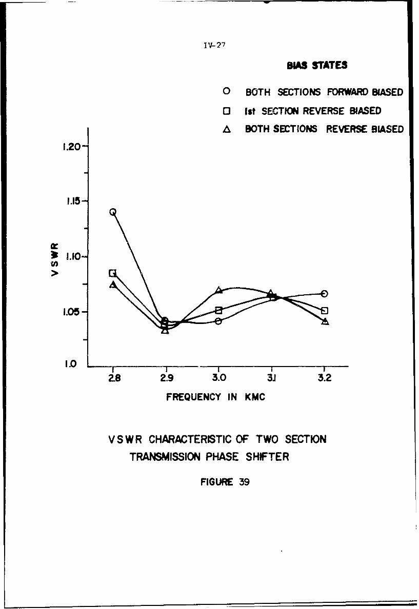
c. Measured Performance of Exrerimental Models: The phase
shift to be obtained from a pair of the switched susceptances described
is proportional to the characteristic line impedance in which they are
mounted provided that the magnitude of switched susceptance is small in
comparison to the characteristic admittance of the transmission line. A
two-section phase shifter using four similar diodes spaced in pairs by
about a quarter wavelength was constructed as may be seen in the photo-
graph of Figure (36). Measurements of phase shift, insertion loss andi
input VSWR made over the frequency range 2800 Mc to 3200 Mc are also shown
in Figres (37), '38) and (39) respectively. The characteristic impedance

IV-29
in the ina section in which the diodes were mounted was 3.3 ohms. Brcad-
band, three section, quarter wavelength, coaxial line transformers having
a Tchebyscheff dIstribution of reflection coefficients as each end of the
diode loaded section were used tc transform this low impedance tc the
50 ohm impedance of the measurement eouipment.
As may be seen from Figure (37), the phase shift was
approximately equal to 110 per section. This was expected since the
normalized switch susceptances are ±j C.1 for an estimated phase shift
of 0.2 radians or about 110. The measured insertion loss and VSWR of the
transformer and phase shifter aggregate is seen to be less than .. 3 deci-
bels and 1.18 over the 14% frequency band. 'The contributions ro these
values resulting from the transformer and low impedance line circait with
diodes removed were neasured independently and found to be 0.25 decibels
insertion loss and 1.10 maximum VSWR over the same frequency range. Thus,
the diodes are seen to impart the desired phase shift function with mini-
mal mismatch and insertion loss contributions to the circuit in which
they are mounted.
A second experimental model was consti -zd using a trans-
mission line impedance of 6.25 ohms and 16 diodes arranged in 8 pairs,
again with quarter wavelength spacing at 3000 Mc. The photograph of this
model is shown in Figure (40). The insertion loss and input VSWR of this
circuit measured with the diodes removed is as shown in Figure (41). From
this, it is seen that increasing the length of the low impedance section
does not appreciably increase the insertion loss or input VSWR. Thus, a

BLANK PAGE

I 'I- O
w
aL.
z00
c Z
z
LL.0
a-
0X-0L

IV- 31
1.0
-0.800.6
(0oj 0.400
0.2 0 0Ze 0 0
1.8
r 1.6
' 1.4
- 1.2
1.0 a i l I9! t 12000 2500 3000 3500 4000
FREQUENCY (Mc)
PERFORMANCE OF S- BAND 8 SECTION ITERATIVE PHASESHIFTER WITH DIODES REMOVED
FIGURE 41

I
IV-32
multi-section phase shifter circuit is even more efficient in that
lesser insertion loss per phase shift section results as the total number
of sections is increased.
The same values of capacity and inductance are asso-
ciated with the diode and its mount as applied for the 3.3 ohm model;
these are 0.8 picofarads and 1.8 nanohenries. Since the characteristic
impedance of the transmission line, however, was twice the value of that
used previously, about 220 of phase shift per section would be expected.
Indeed, this is verified by the measured characteristic shown in Figure
(42). Again, a small variation of phase shift obtained for various fre-
quencies is exhibited. In this case, the total variation in phase shift
obtained over the 14% frequency bandwidth from 2800 Mc to 3200 Mc is only
about 4J%. Some of this variation may have occurred due to the variations
in parameters of the individual iodes used. Typical variations of the
diode capacity values were ±0.1 picofarads. Uirect measurement of the
mount and diode package series inductance is not estimable accurately,
since the diodes represent only small perturbations to the transmission
line. All mounts were adjusted so as to be mechanically similar and thus,
variations of the mount inductance as well as the diode package inductances
are assumed to be small.
The maximum value of input VSWR to this 8-section phase
shifter was 1.3 for all of the bias states examined. As seen from Fig-
ure (42), the maximum value of insertion loss was approximately 0.9 deci-
bels and the minimum value of 0.6 decibels. Approximately 0.3 decibels

/4/160- /BU U \
\"iIj/
140 LHIGH POWER TEST
120. FREQ. 3000 MC-PULSE I/JiSEC
1.. 0 DUTY CYCLE .001
< 80-m
4-FREQUENCY MC SYMBOL
40-/
2800 1
20- 3000 03200
04
(20 0R .53
NUMLER OF REVERSE BIASED SECTIONS
(OTHER SECTIONS FORWARD BIASED)
FIGURE 42
S-BAND TRANSMISSION PHASE SHIFTER PERFOMAC

:V- 34
may be attributed to the ircuft losses with diodes removed; and thus,
an insertion loss of about r.1 decibel per diode Dair resulted. This
suggests that :he un- oalei Q :f each L3 line loading element was approxi-
mately 2C and each diode dissipates about 1% of the power transmitted
along the line.
Thus, a 1 kilowat continuous RF power level would be
estimated sustainable by this S-band phase shifter model, allowing that
each diode could dissipate 1C watts continuously. This is the same con-
tinuous power rating expected of the L-band model. The anomaly of equal
continuous power handling capability achieved by L and S-band models
resulted from the practical fact that the L-band phae shifter did not
have equal loss under forward and reverse bias. If characteristic
impedance levels of main line and stubs had been chosen to effect equal
loss for both bias states of the L-band model, even higher continuous
power levels could be sustained.
The unloaded Q value of 20 represented by the S-band
switched susceptance elements implies that the diode resistance values,
RF and R., were approximately equal at 3000 Mc and had a value of about
1.5 ohms. They were similar to the diodes used in the L-band model for
which unequal resistances are measured at L-band for forward and reverse
bias. The loss mechanisms of the diode are indicated by this measure-
ment to be such as to cause the effective forward bias resistance to
increase and the reverse resistance to decrease with frequency, causing
them to be near equal at O-sand.

IV- 35
Such behaviour might be explained by noting that skin
effect causes the forward biased resistance to increase while the increas-
ing shwit susceptance of the package capacity improves the q of the re-
versed biased diode and decreases the apparent series resist.nce of the
simplified model shown in Figure (42). Also, the series RG representa-
tion for the reversed biasei diode 'inction. itself, is an approximation
which represents the combined diode package contact losses and losses in
the Intrinsic region; the former in:reases with frequency and the latter
decreases with frequency.
Since the diode resistance measurements are somewhat
difficult to make due to the relatively high Q of the PIN dilde at micro-
wave frequencies, these phase shif r insertion loss measurements provide
a useful approximate measurement of the absolute valua of the diode resis-
tances for forward and reverse bias at 3000 Mc.
d. Voltage Limited Peak Power Capability: Reference to the
equivalent circuit for this LC susceptance implementation used in the
S-band phase shifter models, see Figure (34), indicates that if the reac-
tance, j , has a magnitude half that of JXc, then an RF voltage is im-
preskid across the capacitor, in this case the diode junction, equal to
twice the line voltage neglecting resistive losses. This is true no
mattsr what value of characteristic impedance line might be used. How-
ever, for a given operating power level, the line voltage varies inverse-
ly with the square root of the line impedance and thus, the voltage
limited peak power handling capabilities should vary inversely with the

IV-36
characteristic impedance of the main transmission line.
Experimental verification of this expectation was
evidenced. In the two-section, four diode, 3.25 ohm model previously
described, diodes having volt.'ge breakdown values of about 900 volts
were used. These, when reverse biased at -100 volts, were estimated
to sustain a maximum applied RF voltage of 5(0 volts rms. Thus, the
line voltage allowably could reach 280 volts rms in the 3,25 ohm sec-
tion and a barnout peak power capability for the two-section phase
shifter then would be estimated at 21 kilowatts. This is considerably
lower than the 37 kilowatt measured failure point and the discrepancy
may have resulted because the package capacity and junction capacity
values were lumped together In the equivalent circuit model. The pack-
age capacity, of the order of C.3 picofarads, carries an appreciable
fraction of the current in the susceptance branch and the resulting
voltage build-up across the Junction capacitor is accordingly less than
that which would result were all currert to take the path through the
junction reactance, jXC 4
The variation of peak power capability, however, was
verified in that the 6.25 ohm phase shifter model using similar diodes
sustained approximately half the power of the 3.25 ohm model. The six-
teen section phase shifter was tested to a burnout of peak power of 16
kilowatts. Failure mechanisms in both models was manifest as a perma-
nent degradation of the voltage breakdown characteristic of the diodes
after the high power had been applied under the reverse-bias conditions.

IV-37
characteristic impedance of the main transmission line.
Experimental verification of this expectation was
evidenced. in the two-section, four diode, 3.25 ohm model previously
described, diodes having voltage breakdown values of about 900 volts
were used. These, when reverse biased at -100 volts, were estiated
to sustain a maximum applied RF voltage of 560 volts rms. Thus, the
line voltage allowably could reach 280 volts rms in the 3.25 ohm sec-
tion and a burnout peak power capability for the two-section phase
shifter then would be estimated at 24- kilowatts. This is considerably
*i lower than The 37 kilowatt measured failure point and the discrepancy
may have resulted because the package capacity and junction capacity
values were lumped together in the equivalent circuit modal. The pack-
age capacity, of the order of 0.3 picofarads, carries an appreciable
fracition of the current in the susceptance branch and the resulting
voltage build-up across the junction capacitor is accordingly less than
that which would result were all current to take the path through the
junction reactance, jX0.
The variation of peak power capability, however, was
verified in that the 6.25 ohm phase shifter model using similar diodes
sustained approximately half the power of the 3.25 ohm model. The six-
teen section phase shifter was tested to a burnout of peak power of 16
kilowatts. Failure mechanisms in both models was manifest as a perma-
nent degradation of the voltage breakdown characteristic of the diodes
after the high power had been applied under the reverse-bias conditions.

V CONCLUSIONS
Microwave phase control circuit modes examined may be divided con-
veniently into two classes. The first ccas_3ered utilizes the directive
properties of a circuaJtor or hybrid coupler to effect matched trans-
mission from a network of c.ntroliel reflection coefficient. This may
be considered the t.--ns~ssion refflect-on mode. A secend basic circuit
effects phase control by per-ii.i'!y spaced, variable reactance elements
along the transmission line. Spacings ca-. be cnosen to Dermit matched
transmission over a broad bandwi-h.
The transmission reflection mode is part'imi.iarly useful ftor ismle-
menting a continuously variable phase shifter. This vas accomplished
using terminating networks of a hyiorid coupler which containei varactor
diodes. Their variable capacity with reverse bias permitted realiza-
tion of 00 to 1800 phase shifters at L and S-bands which were found to
have a defined Figure of Merit, F, given approximately by
F = . degrees jDiode cut-off Freouency)F= (decibel of loss 1 Operating Frequency
Power level of linear operation was limited to about 1 watt due to the
varactor diode's rapid capacity change with applied voltage.
The discrete increment or step phase shifter using PIN diodes did
not manifest nonlinear microwave characteristics even at levels exceed-
ing 100 kilowatts with tens of amperes and hundreds of volts applied
within a pulse. Transmission reflection phase shifter circuits which
used hybrid terminating networks which -,ere essentially switched delay
lines were constructed. RF peak power levels of 2.5 to 48 kilowatts

V-2
were sustained with phase shift values of 1800 and 21.50 respectively.
In general, peak power capability is inversely proportional to the square
of the phase shift obtained. Insertion loss, in principle, may be reduced
along with phase shift provided lesser values of phase shift are obtained
but changes in the circuit impedance levels are necessary.
Operation at increasing RF power levels with reduced values of phase
shift obtained per diode suggests the hybrid coupler or circulator compo-
nent may be eliminated giving rise to the transmission phase shifter mode.
Two basic models of this circuit were constructed, one at L-band and
one at S-band. The former utilized switchable length stubs along the
main transmission path to effect the necessary controlled susceptance
line shunting pairs of the prototype circuit. High power operation up
to l4O kilowatts was thusly achieved at L-band. Even more importantly
fox, phased array beam steering applications, the insertion loss values
were lower than those obtained with the transmission reflection mode
models. A 15 kilowatt peak power, 1 kilowatt continuous power (esti-
mated continuous rating) phase shifter which yielded 0 to 1800 phase
shift in 8 equal steps had only 0.7 decibels maximum loss, and 0.5 deci-
bels average loss.
The second transmission mode model was designed using the inherent
reactances of the PIN diode as switchable phase controlling elements and
a~surned the simple configuration of a low impedance transmission line
with shunt mounted diodes iteratively spaced at quarter wavelength inter-
vals. Likewise, this circuit produced desirable characteristics as a

I
V-3
control element for a high power array antenna. A 6.25 ohm lire shunted
by 16 diodes provided C0 to 1800 phase shift at up to 15 kilowatts peak
power and IOX watts (estimated) continuous power with a maximum total
insertion loss of only :.9 decibels.
in short, microwave - miconductor phase control, particularly in
the L and S frequency bands readily is feasible both for low power
applications such as automatic instrumentation, countermeasures and
trimmer requirements in parallel tube chains as well as high power appli-
cations in which the phased array antenna is prominent, as an example.

VI-!
VI BIBLIOGRAPHY
1. S. B. Cohn, P. M. Sherk, J. K. Shimizu and E. M. T. Jones,"Strip Transmission Lines and Componentst', Feb. 1957, FinalReport - Stanford Research Project 1114, Stanford ResearchInstitute, Menlo Park, California.
2. R. H. Hardin, E. J. Downey, J. Munushian, "Electronically-Variable Phase Shifters Utilizing Variable Capacitance Diodes",Proc. I.R.E., May, 1960, pp. 944-945.
3. A. J. Simmons, "Phase Shift by Periodic Loading of Waveguideand Its Application to Broad Band Circular Polarizati on",I.R.E. Trans MTT, Dec., 1955.
4. K. E. Mortenson, "Transistor Junction Temperature as a Functionof Time", Proc. I.R.E., April 1957.
5. H. N. Dawirs and W. G. Swarner, "A Very Fast, Voltage ControlledMicrowave Phase Shifter", The Microwave Journal, June 1962.
6. J. F. White, "Semiconductor Microwave Phase Control", NEREMRecord, 1963.
7. J. F. White, "A Diode Phase Shifter for Array Antenna", Digestof 1964 International Symposium of IEEE, MTT Group.
8. M. E. Hines, "Fundamental Limitations of Diode Switching" paperto be published in the Proc. IEEE.
9. L. Stark, R. Burns, et al, "Phased Array Study", Hughes Air-craft -Company Study Report, Contract Number N0bsr-89427.
10. E. J. Wilkinson, L. I. Parad, W. R. Connervey, "An X-BandElectronically Steerable Phased Array", The Microwave Journal,February 1964.
11. Leo Young, "Tables for Cascaded Homogenous Quarter-Wave Trans-formers", IRE Trans MTT, April 1960.
12. S. B. Cohn, "Optimum Design of Stepped Transmission-Line Trans-formers", IRE Trans MTT, April 1955.
13. R. E. Collin, "Theory and Design of Wide-band MultisectionQuarter-Wave Transformers", Proc. I.R.E., February 1955.

VI-2
14. J. Riblet, "General Synthesis of Quarter-Wave Impedance Trans-formers", I.R.E. Trans MTT, January 1957.
15. K. E. Mortenson, "Microwave Semiconductor Control Devices",The Microwave Journal, May 1964.
16, R. V. Garver, E. G. Spencer and M. A. Harper, "Microwave Semi-conductor Switching Techniques", I.R.E. Trans. MTT, October 1958.
17. M. R. Barber, "A High Power Protector Using PIN Diodes", Diestof IEEE MTT Symposium 1963.
18. F. Reggia and E. G. Spencer, "A New Technique in Ferrite PhaseShifting for Beam Scanning of Microwave Antennas", Proc. I.R.E.,November 1957.

Contract sr - 87291
Chief, Burau of ShipsWashington 25, D. C.Attn: Code 681A2B IAttnt Code 684 1Attnt Code 335 1
Chief, Bureau of WeaponsWashington 25, D. C.
Director, Naval Electronics LaboratorySan Diego 52, California
Director, Naval Research LaboratoryWashington 25, D. C.Attn: Code 5250
Commanding GeneralU. S. Army Signal Research & Development Labs.Fort Monmouth, New JerseyAttn: SIGFV/EL-PEE Mr. N. Kipatz
Commanding OfficerDiamond Fuse LaboratoriesConnecticut Ave. & Van Ness St., N. W,Washington 25, D. C.Attn: Code 250 1
Comaanding GeneralWright Air Development CenterWright-Patterson Air Force Base, OhioAttn: WWDPVE-l Wr. G. Duree 1
Commanding GeneralRome Air Development CenterGriffiss Air Force Base, New YorkAttn: M~r. P. Romanelli 1
Commanding GeneralAir Force Cambridge Research CenterAir Research & Development CommandL. G. Hanscom FieldBedford, Mass. Vr. C. E. Ellis I
Advisory Group on Electron Divices346 BroadwayNew York, N. Y. 3

-2-
.ofcoi
Armed Services Technical Information AgencyArlington HallArlington, Virginia 7
Commander (Code 753)U. S. Naval Ordnance Te,t StationChina Lake, CalfforniaAttn: Technical Library I
New %,exico State UniversityPhysical Science LaboratoryBox 548University ParkNew Mexico