Cleanroom Facilities: Experience from an usernanocenter.eng.wayne.edu/Nano workshop...Cleanroom...
25
WAYNE STATE UNIVERSITY Cheng Cleanroom 8/2 Cleanroom Facilities: Experience from an user Mark Ming-Cheng Cheng Electrical and Computer Engineering Wayne State University Detroit MI USA [email protected]
Transcript of Cleanroom Facilities: Experience from an usernanocenter.eng.wayne.edu/Nano workshop...Cleanroom...

WAYNE STATE UNIVERSITY Cheng Cleanroom 8/2
Cleanroom Facilities:
Experience from an user
Mark Ming-Cheng Cheng
Electrical and Computer EngineeringWayne State University
Detroit MI [email protected]

Thin Film Deposition
Microfabrication is the term that describes processes of fabrication of
miniature structures, of mironmeter sizes and smaller. Historically the earliest
microfabrication processes were used for integrated circuit fabrication, also
known as “semiconductor manufacturing”, ” microelectronic fabrication”, ”VLSI
technology”.
Micro/Nano Fabrication
WAYNE STATE UNIVERSITY Cheng Cleanroom
2 cores; Introduced 20061.8 ~3GHz
291 millions transistorsDie size 111mm2; 65W
65nm

In the last two decades, microfabrication has been used in many research fields, including
* Micro Electromechanical System (MEMS)
* RF MEMS (resonators, filters, switches, phase shifters)
* Microfluidics/ Lab-on-Chip
* Bio MEMS
* Solar cells
* Flat panel display
* NEMS
Thin Film DepositionMicro/Nano Fabrication
WAYNE STATE UNIVERSITY Cheng Cleanroom

Thin Film DepositionEnabling Technology in iPhone
WAYNE STATE UNIVERSITY Cheng Cleanroom
Microphone
Accelerometer
GPU (graphic processor) 45nm

Thin Film DepositionHow to Make Sandwiches?
WAYNE STATE UNIVERSITY Cheng Cleanroom
METHOD AND APPARATUS FOR MAKING A SANDWICHInternational Publication Number WO 2006/068865 AW Section (54)
Add breadCut bread
Cut vegetablesPlace vegetables
…

How to Make Devices?
WAYNE STATE UNIVERSITY Cheng Cleanroom
/etching
Deposition ModulePhotolightography Module (Pattern Transfer)
Etching Module
pMOS
Materials
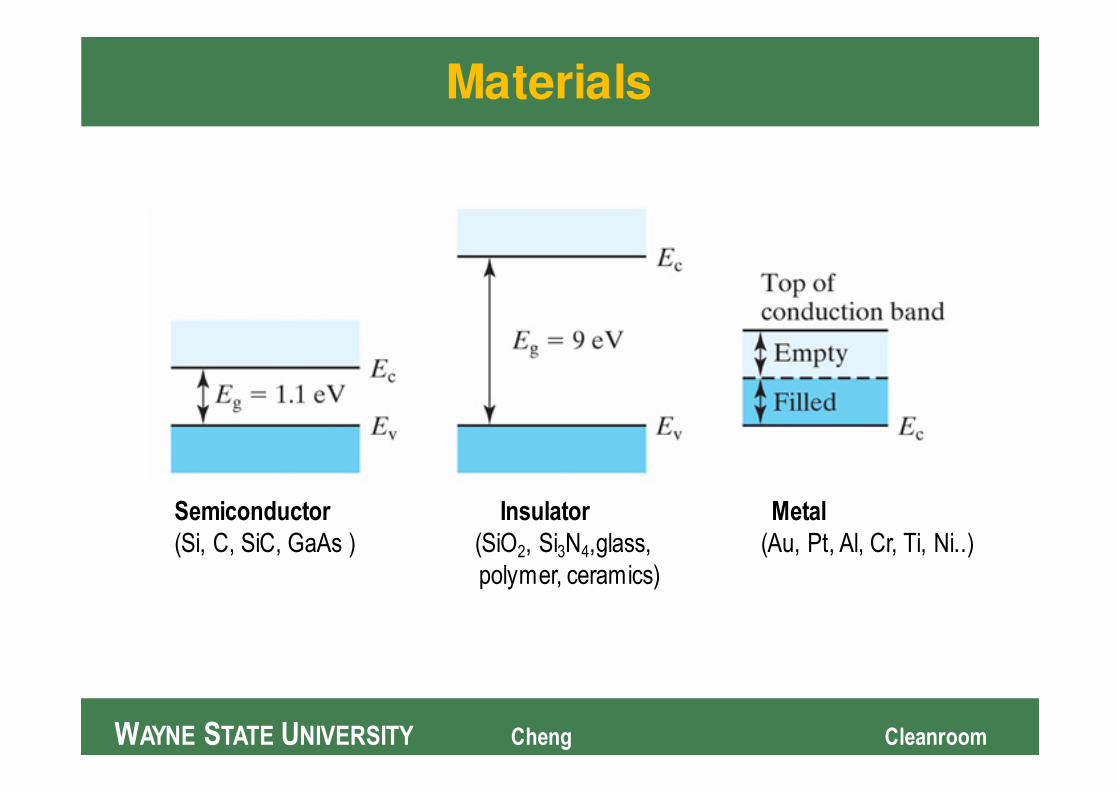
WAYNE STATE UNIVERSITY Cheng Cleanroom
Semiconductor Insulator Metal
(Si, C, SiC, GaAs ) (SiO2, Si3N4,glass, (Au, Pt, Al, Cr, Ti, Ni..)
polymer, ceramics)

Thin Film Deposition (overview)
WAYNE STATE UNIVERSITY Cheng Cleanroom
I. Furnace (Few hundred~11000C, atmosphere): SiO2, P++
II. Low Pressure Chemical Vapor Deposition System (LPCVD):
polycrystalline Si, amorphous SiO2
III. Plasma Enhanced Chemical Vapor Deposition System (PECVD):amorphous Si, nitride, SiO2
IV. E-beam Evaporator: metals (Al, Cr, Cu, Au, Ni, Pt, Ti, Mo),Si, Ge
V. Sputtering: Target Ti, Al, Al with 1%Si, 1%Cu), Mo, Au, Pt, Ta, Ni, Co, Cr,
Si, Pyrex, ITO Gas Ar, N2, O2

Furnace
WAYNE STATE UNIVERSITY Cheng Cleanroom
Few hundred~11000C, atmosphere Thermal oxide (dry): excellent electrical property,
10nm~300nm
Thermal oxide (wet): 100nm~1-2µm
Boron diffusion (BN source):boron doping, P++
etching stop
Metal annealing (N2 gas)
22OSOS
ii→+

Low Pressure Chemical Vapor Deposition
WAYNE STATE UNIVERSITY Cheng Cleanroom
I . Polysilicon
Pressure 50-150Pa
Deposition rate 100~2000A/min, 600~6500C
Polycrystalline Si ~2µm
Polysilicon is widely used as metal gate in CMOS as
well as structural layers in MEMS.
II. Low temperature oxide (LTO)
SiH4
600o
C → Si + 2H
2
22
400
242HSiOOSiH
Co
+ →+

Plasma Enhanced Chemical Vapor Deposition
WAYNE STATE UNIVERSITY Cheng Cleanroom
Reaction Gas SiH4, NH3, N2O
Power max 400W
Temperature 25~3000C
Deposited Materials
α-Si : gas SiH4
SixNy: gas SiH4, NH3
SixOy: gas SiH4, N2O
SiOxNy: gas SiH4, NH3, N2O
Typically used for depositing passivation layers
Deposition rate 4000A/min (deepening on power and temp)
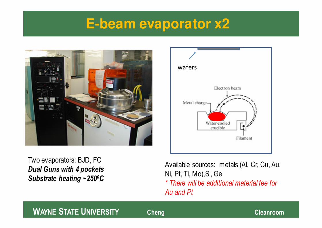
E-beam evaporator x2
WAYNE STATE UNIVERSITY Cheng Cleanroom
Two evaporators: BJD, FC
Dual Guns with 4 pockets
Substrate heating ~2500C
Available sources: metals (Al, Cr, Cu, Au,
Ni, Pt, Ti, Mo),Si, Ge
* There will be additional material fee for
Au and Pt
wafers

WAYNE STATE UNIVERSITY Cheng Cleanroom
Photographic Process

Photolithography
WAYNE STATE UNIVERSITY Cheng Cleanroom
Contact Aligner
Provide alignment in x,y,z directions
Exposure resolution ~0.8µm
“ Print with the light”
Light sensitive film
Cr mask in contact with wafers

Photolithography (steps)
WAYNE STATE UNIVERSITY Cheng Cleanroom
I. Spin-coating PR II. Soft Bake
III. Alignment/Exposure
IV. Developer
(Selectively remove PR)

SU-8
WAYNE STATE UNIVERSITY Cheng Cleanroom
SU-8 ( from Microchem)A viscos polymer that can be spin-
coated and produce microstructures
Negative PhotoresistThickness 1~300µm
Microstructures with high aspect ratio
20

Thin Film Etching (Overview)
WAYNE STATE UNIVERSITY Cheng Cleanroom
I. Wet etching, isotropic etching: Au etch, Al etch, Cr etch, Ni etch
II. Wet etching, anisotropic etching (bulk micromachining): TMAH etch
III. Metal Lift-off
VI. RCA clean: wafer cleaning
V. Dry etching, anisotropic etching
LAM etcher ( polysilicon, nitride, SiO2)DRIE (silicon); high aspect ratio silicon microstructures.
VI . Dry etching, isotropic etching
Drytech (PR, PDMS)
XeF2 (silicon)
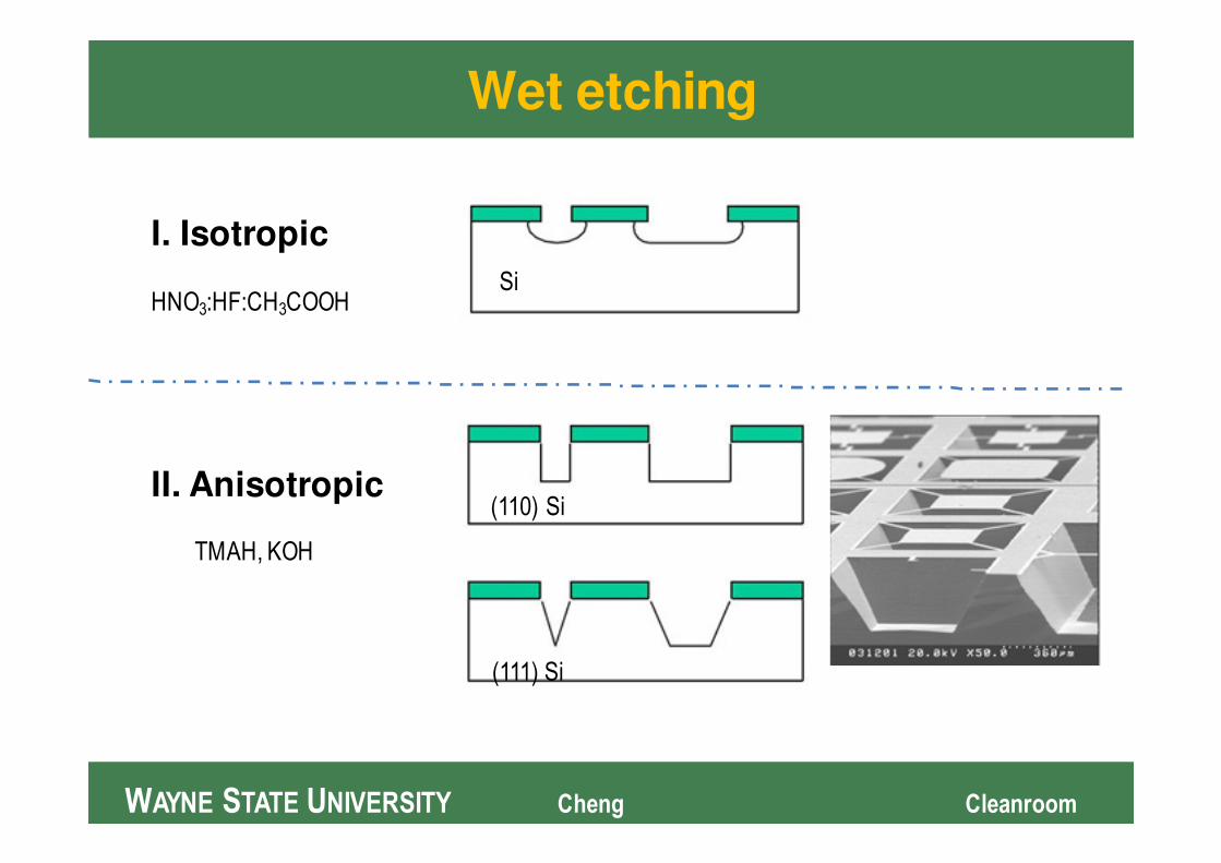
Wet etching
WAYNE STATE UNIVERSITY Cheng Cleanroom
I. Isotropic
II. Anisotropic
Substrate orientation
Crystal Plane
Orientation
TMAH, KOH
SiHNO3:HF:CH3COOH
(110) Si
(111) Si
WAYNE STATE UNIVERSITY Cheng Cleanroom
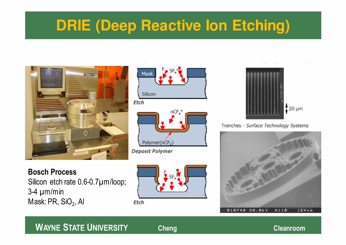
DRIE (Deep Reactive Ion Etching)
Bosch Process
Silicon etch rate 0.6-0.7µm/loop;
3-4 µm/min
Mask: PR, SiO2, Al

Drytech
WAYNE STATE UNIVERSITY Cheng Cleanroom
Dry Isotropic etching of polymers (Oxygen
plasma, Asher)
Reaction gas: O2, Ar, CF4
Power Max 300W
Oxygen plasma is widely used for
(1)Substrate cleaning
(2)Removal of PR(3)Removal of polymer/organic materials
(4)PDMS bonding

XeF2
WAYNE STATE UNIVERSITY Cheng Cleanroom
Xenon Difluoride (XeF2) Etching • Home-made equipment (Cheng, Xu)
• Dry, Isotropic etching of Si
2XeF2 + Si →2Xe + SiF4
• High selectivity for Al, SiO2, Si3N4,PR,PSG
• Typical etch rates of 1 to 3 µm/min
• XeF2 reacts with water (or vapor) to form HF

Other Capabilities
WAYNE STATE UNIVERSITY Cheng Cleanroom
Packaging
Characterization
Wafer Bonder Dicing Saw Wire Bonder
Surface Profiler Interferometer

On-Going Projects
WAYNE STATE UNIVERSITY Cheng Cleanroom
Dr Yong Xu (Joined Wayne State 2002)
NSF ECCS A novel 3-dimensional neural probe technology combining electrical and chemical
interfaces (PI)
NSF CMMI Collaborative Research: Fish-Inspired Ultra-Sensitive Infrasound Sensor for Critical
Infrastructure Monitoring and Geo-Hazards Early Warning (PI)
NSF ECCS CAREER: Wearable accelerometers for continuous respiratory sound monitoring (PI)
NIH R21 Development of a neurotransmitter based epiretinal prosthesis (co-PI)
NSF CBET Neurophysiologically-based computational platform for the characterization and
optimization of retinal prosthetic stimulation (Co-PI)
Dr Amar Basu (Joined Wayne State 2008)
NSF CBET Microfrationation in Droplets (FD) - Linking Proteomic Separations to High
Throughput Functional Screening (PI)
Dr Mark Ming-Cheng Cheng (Joined Wayne State 2008)
NSF CBET CAREER: A Robust, Chronic Neural Prosthesis Using High-Capacity Graphene
Electrodes and Biodegradable Silicon Support (PI)
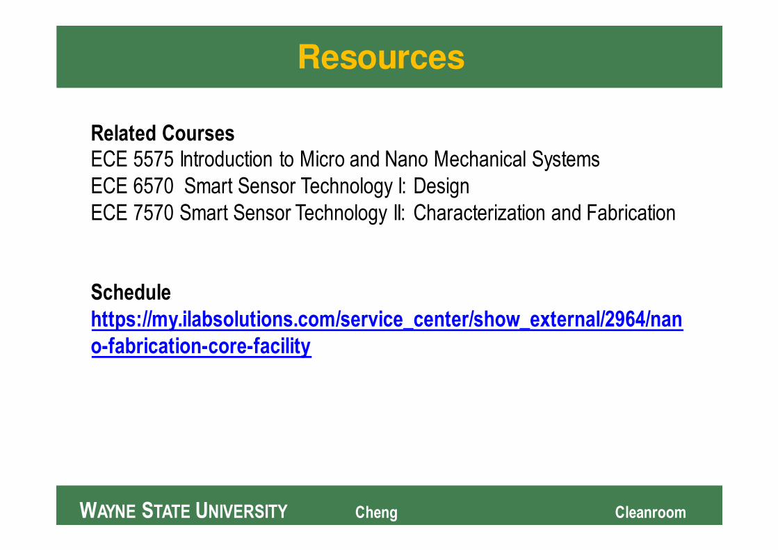
Resources
WAYNE STATE UNIVERSITY Cheng Cleanroom
Related CoursesECE 5575 Introduction to Micro and Nano Mechanical Systems
ECE 6570 Smart Sensor Technology I: Design
ECE 7570 Smart Sensor Technology II: Characterization and Fabrication
Schedule
https://my.ilabsolutions.com/service_center/show_external/2964/nan
o-fabrication-core-facility

Nanotechnology
WAYNE STATE UNIVERSITY Cheng Cleanroom
Nanotechnology deals with structures sized between 1 to 100 nanometers in
at least one dimension, and involves developing materials or devices
possessing at least one dimension within that size.