
Class: VME USER MANUAL RF2TTC V3 User Manual...
36
Page1 Class: VME Function: RF2TTC PH/ESS document No: Created : 11.10.2006 Page Page 1 of 36 PH-ESE-18-03-2011 Modified: 18.03.2011 Rev.No. 5.3 USER MANUAL RF2TTC V3 User Manual V5.3 RF to TTC VMEbus Interface Card and S/W Summary: This document describes the functionality of the RF2TTC card as well as the generic S/W that has been developed for it. Document Revision 5.3 – o 12.03.07 o : the CR/CSR space has been transposed to the User Space. 16.05.07 o (rev 4): geographical address modified, information on orbit period counter results, initialisation procedure (section 2.7.1), last firmware version, output signals amplitude adjustments (section 2.6), etc… 24.06.09 Information about DAC registers for clock input has been removed (does not exist since V1 of the board) (rev 5.0): BSET and BCLEAR register definition changed to allow individual resetting of QPLLs Last firmware version is 19052009 Default values of QPLL modes If an error occurs, the QPLL_status remains at ‘1’ until having been read o Precisions about orbit delays o Correction on TTCrx read control register example o 25.06.09 o (rev 5.1): Modification on orb length: now, all the orbits are 25ns pulses by default. 14.07.09 (rev 5.2) o : small corrections in the orb delay25 calibration procedures and details on FIFO status 18.03.11 (rev 5.3): small correction page 12, on the Note of the ORB_COARSE_DELAY register Prepared by : Markus Joos, PH/ESS Checked by : Approved by : for information, you can contact : Tel. Fax. E-Mail Sophie Baron +41.22.7677339 +41.22.7678925 [email protected] Markus Joos +41.22.7672364 +41.22.7678925 [email protected] Stephane Detraz +41.22.7679702 +41.22.7678925 [email protected]
-
Upload
nguyendieu -
Category
Documents
-
view
222 -
download
3
Transcript of Class: VME USER MANUAL RF2TTC V3 User Manual...
Page
1
Class: VME
Function: RF2TTC
PH/ESS document No: Created : 11.10.2006 Page Page 1 of 36
PH-ESE-18-03-2011 Modified: 18.03.2011 Rev.No. 5.3
USER MANUAL
RF2TTC V3
User Manual V5.3
RF to TTC VMEbus Interface Card and S/W
Summary:
This document describes the functionality of the RF2TTC card as well as the generic S/W that has been developed for it. Document Revision 5.3 –
o 12.03.07o
: the CR/CSR space has been transposed to the User Space. 16.05.07
o
(rev 4): geographical address modified, information on orbit period counter results, initialisation procedure (section 2.7.1), last firmware version, output signals amplitude adjustments (section 2.6), etc… 24.06.09
Information about DAC registers for clock input has been removed (does not exist since V1 of the board)
(rev 5.0):
BSET and BCLEAR register definition changed to allow individual resetting of QPLLs Last firmware version is 19052009 Default values of QPLL modes If an error occurs, the QPLL_status remains at ‘1’ until having been read
o Precisions about orbit delays o Correction on TTCrx read control register example o 25.06.09o
(rev 5.1): Modification on orb length: now, all the orbits are 25ns pulses by default. 14.07.09 (rev 5.2)
o : small corrections in the orb delay25 calibration procedures and details on FIFO status
18.03.11
(rev 5.3): small correction page 12, on the Note of the ORB_COARSE_DELAY register
Prepared by :
Markus Joos, PH/ESS
Checked by :
Approved by :
for information, you can contact :
Tel. Fax. E-Mail
Sophie Baron +41.22.7677339 +41.22.7678925 [email protected]
Markus Joos +41.22.7672364 +41.22.7678925 [email protected]
Stephane Detraz +41.22.7679702 +41.22.7678925 [email protected]

Page
2
Table of Contents 1. Introduction ............................................................................................................................................. 3
2. RF2TTC Hardware ................................................................................................................................. 5
2.1. Standards and power supplies ........................................................................................................................ 5
2.2. VMEbus interface ............................................................................................................................................ 5 2.2.1. Reset registers ............................................................................................................................................................. 6
BSET: Board Set Register assignment .................................................................................................................................... 6 BCLEAR (User-defined BCLEAR) Register assignment ....................................................................................................... 7
2.2.2. Board Identification read only registers ...................................................................................................................... 8 2.2.3. Board configuration registers ...................................................................................................................................... 8
BCx_MAN_SELECT, BCx_BEAM_SELECT & BCx_NOBEAM_SELECT ...................................................................... 8 BCx_QPLL_MODE ................................................................................................................................................................ 9 BCx_QPLL_STATUS .......................................................................................................................................................... 10 ORBx_MAN_SELECT, ORBx_BEAM_SELECT & ORBx_NOBEAM_SELECT ............................................................ 11 ORBx_POLARITY ............................................................................................................................................................... 12 ORBx_COARSE_DELAY ................................................................................................................................................... 12 ORBx_LENGTH .................................................................................................................................................................. 12 ORBx_INT_PERIOD_SET .................................................................................................................................................. 13 ORBx_INT_PERIOD_COUNTER....................................................................................................................................... 13 ORBx_COUNTER................................................................................................................................................................ 13 ORBx_PERIOD_RD ............................................................................................................................................................ 13 ORBx_PERIOD_FIFO_STATUS ........................................................................................................................................ 14 ORBx_PERIOD_FIFO_RD .................................................................................................................................................. 14 ORBx_DAC .......................................................................................................................................................................... 14 TTCrx_status......................................................................................................................................................................... 15 BST_Beam_Mode................................................................................................................................................................. 15 BEAM_NO_BEAM_DEF .................................................................................................................................................... 16 WORKING_MODE.............................................................................................................................................................. 17 ORB_INT_ENABLE ............................................................................................................................................................ 17 ORB_COUNTER_ENABLE ................................................................................................................................................ 18 PERIOD_COUNTER_ENABLE .......................................................................................................................................... 18 COUNTERS’ RESET registers ............................................................................................................................................. 19 DELAY25_REG, TTCrx_REG ............................................................................................................................................ 19 BC_ DELAY25_x ................................................................................................................................................................. 20 ORBIN_DELAY25_x ........................................................................................................................................................... 21 ORBOUT_DELAY25_x ....................................................................................................................................................... 21 TTCrx REGISTERS ............................................................................................................................................................. 22
2.3. Calibration procedures .................................................................................................................................. 24 2.3.1. Threshold adjustment (ORBx_DAC) ........................................................................................................................ 24 2.3.2. Orbit inputs delay adjustment .................................................................................................................................... 25
2.4. Fibre / cable connections................................................................................................................................ 28
2.5. Output signal amplitude information........................................................................................................... 29
2.6. Front-panel LEDs ........................................................................................................................................... 29
2.7. Improvements made on the production version ( V3) ................................................................................ 30 2.7.1. Initialisation procedure .............................................................................................................................................. 30
2.8. Registers Summary ........................................................................................................................................ 31
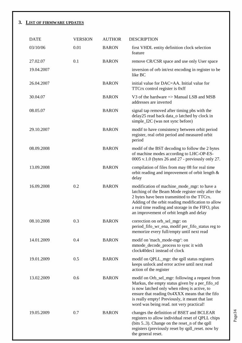
3. List of firmware updates ....................................................................................................................... 34
4. RF2TTC common software .................................................................................................................. 36
4.1. Introduction .................................................................................................................................................... 36 4.1.1. H/W Environment ..................................................................................................................................................... 36 4.1.2. S/W Environment ...................................................................................................................................................... 36
4.2. Test programs ................................................................................................................................................. 36
4.3. The user library .............................................................................................................................................. 36

Page
3
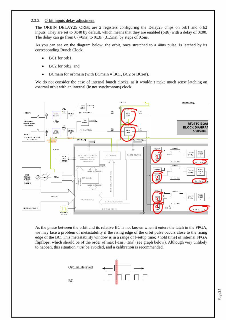
1. INTRODUCTION The RF2TTC (RF to TTC VMEbus Interface Card) is an interface card between the optical receiver modules (receiving timing signals coming from the SR4 building in Echenevex), and the TTC electronics within the experiments.
The timing signals treated by the RF2TTC are the three 40.078MHz Bunch Clocks (BC1, BC2 and BCref) and the two orbit signals (Orb1 and Orb2) necessary to drive the 2 beam lines of the LHC. The RF2TTC module converts them into ECL signals, and performs various adjustments on each signal before making them available for the in-detector TTC electronics.
The three Bunch Clocks (represented on the top part of the following diagram) are all treated in the following way: A comparator with an adjustable threshold first converts the input signal into a PECL signal, before being multiplexed with an internal 40.078MHz clock in case of absence of the Bunch Clock on the front panel. The signal is then shifted by an adjustable delay with 0.5ns precision, before being cleaned by a QPLL and transmitted on the front panel via an ECL 50 Ohm coaxial cable driver with an AC-coupled output. A global multiplexer allows selection between the three Bunch Clocks and the internal clock to generate a fourth Bunch Clock output, called Main BC, which can also be delayed. The two orbit signals (middle and bottom right parts of the diagram) are first converted using the same adjustable comparator stage as for the Bunch Clocks. They are then lengthened to more than 25ns, finely delayed with 0.5ns steps, before going into an FPGA (grey block of the diagram), where they are synchronized to their corresponding clock, multiplexed with an internal orbit, and coarse delayed. Their length and polarity can be adjusted, and they are then again finely delayed before being transmitted by the ECL drivers. A global multiplexer also allows selection between the two orbits and an internal one, synchronized to the Main Bunch Clock. This orbit signal is called Main Orbit and can as well be finely delayed before being transmitted. The BST (Beam Synchronous Timing) optical signal (on the bottom left part of the diagram) is received, decoded and analyzed to recover the machine mode. This mode is useful to know when the timing signals are stable and can be used. In deed, neither the Bunch Clocks nor the Orbit signals are fully guaranteed out of the physics modes (flat top of the LHC energy curve). It is thus advised to use internal signals when the machine mode indicates that there is no beam. All the adjustments are done using VME registers. Many status registers are available, as well as special configurations, for stand-alone or debugging work. This document contains a description of all accessible registers of the RF2TTC card as well as description of the generic S/W that has been developed for this card. At the end of this document, some basic examples of configuration procedures are proposed.

RF2TTC module diagram
text
text
FPGA
MAIN BC CLOCK
BC2 CLOCK
BC1 CLOCK
text
VME BACKPLANE
FROM RF OPTICAL RECEIVERS
INTERNAL CLOCK
Sine2 Square
PhaseAdjust
Sine2 Square
Sine2 Square
PLL&VCXO
PLL&VCXO
ECL Driver
Sine2 Square
Sine2 Square
Stretcher
Stretcher
Fine Delay
Fine Delay
PLL&VCXO
BC1
BC2
BC ref
PECL2NIM
PLL&VCXO
PhaseAdjust
PhaseAdjust
PhaseAdjust
ORBIT1
ORBIT2
VME BUS
MUX2:1
MUX2:1
MUX2:1
FAN1:4
FAN1:4
INTERNALCNT
ECL Driver
ECL2NIM
CoarseDelay
MAIN BC
I2C interface
BC1 ECL/OUT
BC1 NIM/OUT
BC2 ECL/OUT
BC2 NIM/OUT
BCref ECL/OUT
BCref NIM/OUT
MAIN BC ECL/OUT
MAIN BC NIM/OUT
ORBIT1 NECL/OUT
ORBIT1 NIM/OUT
ORBIT2 NECL/OUT
ORBIT2 NIM/OUT
MAIN ORBITNECL/OUT
MAIN ORBITNIM/OUT
Sine pulse1V peak (0-1V)
5ns width
Sinusoidal frequencies40.07XX MHz
varying0.6V pk-pk /8
or 0.6V pk-pk (CMS)
Sinusoidal frequency40.07XX MHz
fixed0.6V pk-pk / 8
or 0.6V pk-pk (CMS)
5ns square pulse
40 ns LVPECL
ECL comparator
AD96685
DELAY25
QPLL
BC & ORBIT SOURCES SELECTION, DACs adjustment for Orbit
comparators
BST decoder
VME INTERFACE
BST SIGNAL
OPTICALTTC
FRAMES
MACHINE MODES
REM
OTE
CO
NTR
OL
S1
S4
D
C2C1 ENB
Multiplexer
MACHINE MODES
FIN
E D
ELA
YS C
ON
TRO
L
MAIN BC
INTERNAL CLOCK
INTERNAL CLOCK
TTCrx
BC1 lock
BC2 lock
BCref lock
MAIN BC lock
BCsel[1..0]
BOARD STATUS
Lock, TTCready, ...
Orbit sel
Orbit sel
BC1 lockBC2 lock
BCref lockMAIN BC lock
Orbit1Orbit2
Machine Mode Run/No
VME accessVME_Berr
BST_ready
MAIN BC int/BC1BC2/Bcref
MAIN ORBIT Or1/Or2/Int
STATUS REGISTERS
BC1sel
BC2sel
BCref sel
I2C
Orbit detect
Orbit detect
Orb2 det
MAIN BCsel[1..0]
RF2TTC BOARDBLOCK DIAGRAM V1.7
5/20/2009
LVPECL2LVDS
LVPECL2LVDS
LVPECL2LVDS
LVDS2ECL
LVDS2ECL
LVDS2ECL
DELAY25
DELAY25
DELAY25
QPLLMUX4:1
LVPECL2LVDS
Adjust. Stretch
er
2.5V CMOS
2.5V CMOS
2.5V CMOS
2.5V CMOS
Diff NECL
LVDS
LVDS
LVDS
LVDS
Orb1 det
Step 500ps, range 25ns
LVPECL QUARTZ80.158MHz
Diff NECL
Diff NECL
AC COUPLING
AC COUPLING
AC COUPLING
Diff LVPECL
Diff LVPECL
Diff LVPECL
Diff LVPECL
AC COUPLING
Diff LVPECL
CAPACITIVE COUPLING + THEVENIN
TERMINATION FOR DC LEVEL OF 1.2V
Diff LVPECL
Diff LVPECL
Diff LVPECL
Diff LVPECL
LVDS 800mV swing
LVDS 800mV swing
LVDS 800mV swing
LVDS 800mV swing
LVDS
LVDS
LVDS
LVDS
MC10EP89 ECL coax cable
drivers
ECL2NIM CONVERSION
USING BSR17A TRANSISTORS
74AHC123
PECL
PECL
PECL
PECL
DACs & Ref
Voltage
V_comp5
5ns square pulse
40 ns LVPECL
ECL2NIM CONVERSION
USING BSR17A TRANSISTORS
v
Q
QSET
CLR
D
Sync
Q
QSET
CLR
D
Sync
Fine Delay
Fine Delay
Fine Delay
S1
S4
D
C2C1 ENB
Multiplexer
CoarseDelay
Adjust. Stretch
er
S1
S4
D
C2C1 ENB
Multiplexer
Q
QSET
CLR
D
Sync
INTERNALCNT
Q
QSET
CLR
D
Sync
INTERNALCNT
CoarseDelay
Adjust. Stretch
er
PLL&VCXO
ECL comparator
AD96685
V_comp3
V_comp1
V_comp4
V_comp2
FAN1:4
LVDS2ECL
BC1_CLOCK
FAN1:4
LVDS2ECL
BC2_CLOCK
FAN1:4
LVDS2ECL
BCref_CLOCK
MC10EP89 ECL coax cable
driversBC1_clock
BC2_clock
LVDS2ECL
NECL
ECL Driver
PECL2NIM
ECL Driver
PECL2NIM
ECL Driver
PECL2NIM
ECL Driver
ECL2NIM
ECL Driver
ECL2NIM

Page
5
2.
2.1.
RF2TTC HARDWARE
STANDARDS AND POWER SUPPLIES
The RF2TTC board is a VME64x 6U board. It requires the following power supplies:
• +3V3: 2.5A
• +5V: 0.3A
• -12V: 1.4A
Total power : 26W
2.2.
VMEBUS INTERFACE
The VMEbus interface of the RF2TTC cards is implemented in its FPGA and based on the VME interface developed by Peter Lichard for the TRT-TTC board (ATLAS). It provides 2 types of VMEbus addressable resources as described in Table 1.
Resource VMEbus access mode Description Control and status registers
A32/D32 with A19=0 and AM-code 0x09
These are the registers that control the behaviour of a RF2TTC card and provide information about its current status.
EPROM A32/D32 with A19=1 and AM-code 0x09
The access to the EPROM is reserved for in-crate reconfiguration.
Table 1: VMEbus resources of the RF2TTC
All the registers of the board are accessible using 0x09 AM (A32, D32). The board address is the geographical address of the module if the manual rotary switches are set to 0x00. The address used to access the user space is hence defined as follows:
ADDRESS SWITCHES A31-A28 A27-A24 A23-A20
SW1=SW2=0x00 0 GEOG ADD
SW1≠0x00 or SW2≠0x00 0 SW2[3..0] (MSB) SW1[7..4] (LSB)
SW1=LSB SW2=MSB
This picture shows a board numbered: 0xF000000

Page
6
2.2.1.
Reset registers
Register Offset Purpose Access
BSET 0x00010 Set reset actions R/W
BCLEAR 0x00014 Clear reset actions W
BSET: Board Set Register assignment Description:
This register is declared in the VME64x as a User-defined Bset register. It is used here to define partial reset functions (QPLL only, Delay25 chips only, TTCrx only). The bit definition is as follows:
Bit Value Write Read
0 1 place Delay25 chips in reset mode Delay25 chips in reset mode
0 no effect Delay25 chips not in reset mode
1 1 x x
0 x x
2 1 place BC1-QPLL chip in reset mode BC1 -QPLL chip in reset mode
0 no effect BC1-QPLL chip not in reset mode
3 1 place BC2-QPLL chip in reset mode BC2 -QPLL chip in reset mode
0 no effect BC2-QPLL chip not in reset mode
4 1 place BCref-QPLL chip in reset mode BCref -QPLL chip in reset mode
0 no effect BCref-QPLL chip not in reset mode
5 1 place BCmain-QPLL chip in reset mode BCmain -QPLL chip in reset mode
0 no effect BCmain-QPLL chip not in reset mode
6 1 place TTCrx chips in reset mode TTCrx chips in reset mode
0 no effect TTCrx chips not in reset mode
7 1 place board in reset mode Board in reset mode
0 no effect Board not in reset mode
Note: When the QPLL are reset using bits 2 to 5, the BCx_QPLL_MODE registers are NOT reset. So the QPLLs are remaining in the mode to which they were previously configured (ie: autorestart or relock after reset).

Page
7
BCLEAR (User-defined BCLEAR) Register assignment Description:
This register is declared in the VME64x as a User-defined Bclear register. It is used here to remove partial reset functions (QPLL only, Delay25 chips only, TTCrx only). The bit definition is as follows:
Bit Value Write Read
0 1 remove Delay25 chips from reset mode Delay25 chips in reset mode
0 no effect Delay25 chips not in reset mode
1 1
0
2 1 remove BC1-QPLL from reset mode BC1-QPLL chip in reset mode
0 no effect BC1-QPLL chip not in reset mode
3 1 remove BC2-QPLL from reset mode BC2-QPLL chip in reset mode
0 no effect BC2-QPLL chip not in reset mode
4 1 remove BCref-QPLL from reset mode BCref-QPLL chip in reset mode
0 no effect BCref-QPLL chip not in reset mode
5 1 remove BCmain-QPLL from reset mode BCmain-QPLL chip in reset mode
0 no effect BCmainQPLL chip not in reset mode
6 1 remove TTCrx chips from reset mode TTCrx chips in reset mode
0 no effect TTCrx chips not in reset mode
7 1 remove Board from reset mode Board in reset mode
0 no effect Board not in reset mode

Page
8
2.2.2.
Board Identification read only registers
Register Address Value Access
MANUFACTURER ID 0x00000 0x00080030 (CERN) R
BOARD ID 0x00004 0x0000016B R
REVISION ID 0x00008 Hardware version
Prototype = 0x2, Production = 0x3
R
PROGRAM ID 0x0000C Firmware date number
Last 19052009 (19 May 2009)
R
2.2.3.
Board configuration registers
BCx_MAN_SELECT, BCx_BEAM_SELECT & BCx_NOBEAM_SELECT Name Offset Size Access
BC1_MAN_SELECT 0x7FBFC 1 bit R/W
BC2_MAN_SELECT 0x7FBCC
BCref_MAN_SELECT 0x7FBAC
BC1_BEAM_SELECT 0x7FBF8
BC2_BEAM_SELECT 0x7FBC8
BCref_BEAM_SELECT 0x7FBA8
BC1_NOBEAM_SELECT 0x7FBF4
BC2_NOBEAM_SELECT 0x7FBC4
BCref_NOBEAM_SELECT 0x7FBA4
BCmain_MAN_SELECT 0x7FB8C 2 bits
BCmain_BEAM_SELECT 0x7FB88
BCmain_NOBEAM_SELECT 0x7FB84
Description:
These registers select the sources of the BC outputs. Only one set of registers is active at a time.
• The BCx_MAN_SELECT registers are active when the BCx is operating in manual mode (defined in WORKING_MODE register).
• The BCx_BEAM_SELECT registers are active when BCx is defined (by WORKING_MODE register) to be ‘automatic’, and the current LHC beam mode (decoded in BST_BEAM_MODE) is declared by BEAM_NO_BEAM_DEF to be “with beam”.
• The BCx_NOBEAM_SELECT registers are active when BCx is defined (by WORKING_MODE register) to be ‘automatic’, and the current LHC beam mode (decoded in BST_BEAM_MODE) is declared by BEAM_NO_BEAM_DEF to be “without beam”.
• The BCx_MAN_SELECT and the BCx_NOBEAM_SELECT registers are set to INTERNAL (=0) by default, and the BCx_BEAM_SELECT register to EXTERNAL (=1).
Page
9
Bit definition for BC1, BC2 and BCref registers
Value Description
0 Output taken from internal 40.078MHz clock (INTERNAL)
1 Output follows the respective BC input (EXTERNAL)
Bit definition for BCmain registers
Value Description
0 Output taken from internal 40.078MHz clock
1 Output follows BCref input
2 Output follows BC2 input
3 Output follows BC1 input
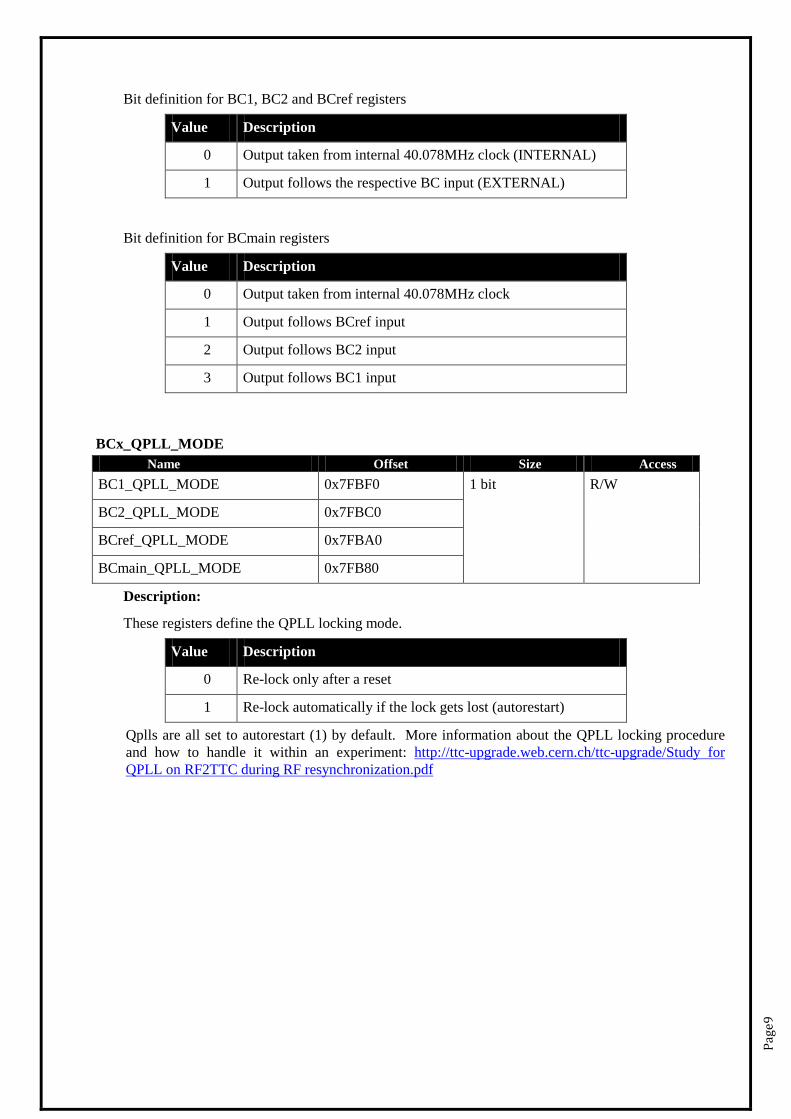
BCx_QPLL_MODE Name Offset Size Access
BC1_QPLL_MODE 0x7FBF0 1 bit R/W
BC2_QPLL_MODE 0x7FBC0
BCref_QPLL_MODE 0x7FBA0
BCmain_QPLL_MODE 0x7FB80
Description:
These registers define the QPLL locking mode.
Value Description
0 Re-lock only after a reset
1 Re-lock automatically if the lock gets lost (autorestart)
Qplls are all set to autorestart (1) by default. More information about the QPLL locking procedure and how to handle it within an experiment: http://ttc-upgrade.web.cern.ch/ttc-upgrade/Study for QPLL on RF2TTC during RF resynchronization.pdf

Page
10
BCx_QPLL_STATUS Name Offset Size Access
BC1_QPLL_STATUS 0x7FBE8 2 bits R
BC2_QPLL_STATUS 0x7FBB8
BCref_QPLL_STATUS 0x7FB98
BCmain_QPLL_STATUS 0x7FB7C
Description:
These registers contain the status of the QPLLs of the BC channels. Bit 1 indicates that the QPLL detected an error and bit 0 indicates the locking status. These error and unlocked bits are latched and, if an error or a loss-of-sync briefly occurs, will remain at ‘1’ until the register has been read.
Bit 1 Description
0 QPLL OK
1 QPLL has error
Bit 0 Description
0 QPLL not locked
1 QPLL locked

Page
11
ORBx_MAN_SELECT, ORBx_BEAM_SELECT & ORBx_NOBEAM_SELECT Name Offset Size Access
ORB1_MAN_SELECT 0x7FB6C 1 bit R/W
ORB2_MAN_SELECT 0x7FB2C
ORB1_BEAM_SELECT 0x7FB68
ORB2_BEAM_SELECT 0x7FB28
ORB1_NOBEAM_SELECT 0x7FB64
ORB2_NOBEAM_SELECT 0x7FB24
ORBmain_MAN_SELECT 0x7FAEC 2 bits
ORBmain_BEAM_SELECT 0x7FAE8
ORBmain_NOBEAM_SELECT 0x7FAE4
Description:
These registers select the sources of the orbit outputs. Only one set of registers is active at any time. The ORBx_MAN_SELECT registers are active when the RF2TTC is operating in manual mode. If the card is in automatic mode and the beam is on the orbit outputs are controlled by the ORBx_BEAM_SELECT registers. The ORBx_NOBEAM_SELECT registers control the orbit outputs when the RF2TTC is in automatic mode and the beam absent. The MAN_SELECT and NO_BEAM registers are set to INTERNAL by default. The BEAM register to EXTERNAL.
Bit definition for ORB1 and ORB2 registers
Value Description
0 Output follows the respective orbit input (EXTERNAL)
1 Output from internal BC synchronized orbit generator
Bit definition for ORBmain registers
Value Description
0 Output follows the orbit 1 input
1 Output follows the orbit 2 input
2 Output from internal orbit generator synchronized to BCmain
Page
12
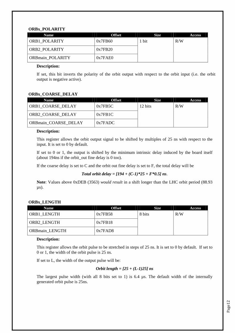
ORBx_POLARITY Name Offset Size Access
ORB1_POLARITY 0x7FB60 1 bit R/W
ORB2_POLARITY 0x7FB20
ORBmain_POLARITY 0x7FAE0
Description:
If set, this bit inverts the polarity of the orbit output with respect to the orbit input (i.e. the orbit output is negative active).
ORBx_COARSE_DELAY Name Offset Size Access
ORB1_COARSE_DELAY 0x7FB5C 12 bits R/W
ORB2_COARSE_DELAY 0x7FB1C
ORBmain_COARSE_DELAY 0x7FADC
Description:
This register allows the orbit output signal to be shifted by multiples of 25 ns with respect to the input. It is set to 0 by default.
If set to 0 or 1, the output is shifted by the minimum intrinsic delay induced by the board itself (about 194ns if the orbit_out fine delay is 0 too).
If the coarse delay is set to C and the orbit out fine delay is set to F, the total delay will be
Total orbit delay = [194 + (C-1)*25 + F*0.5] ns.
Note: Values above 0xDEB (3563) would result in a shift longer than the LHC orbit period (88.93 µs).
ORBx_LENGTH Name Offset Size Access
ORB1_LENGTH 0x7FB58 8 bits R/W
ORB2_LENGTH 0x7FB18
ORBmain_LENGTH 0x7FAD8
Description:
This register allows the orbit pulse to be stretched in steps of 25 ns. It is set to 0 by default. If set to 0 or 1, the width of the orbit pulse is 25 ns.
If set to L, the width of the output pulse will be:
Orbit length = [25 + (L-1)25] ns
The largest pulse width (with all 8 bits set to 1) is 6.4 µs. The default width of the internally generated orbit pulse is 25ns.
Page
13
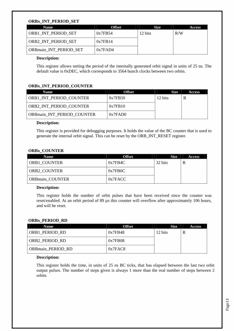
ORBx_INT_PERIOD_SET Name Offset Size Access
ORB1_INT_PERIOD_SET 0x7FB54 12 bits R/W
ORB2_INT_PERIOD_SET 0x7FB14
ORBmain_INT_PERIOD_SET 0x7FAD4
Description:
This register allows setting the period of the internally generated orbit signal in units of 25 ns. The default value is 0xDEC, which corresponds to 3564 bunch clocks between two orbits.
ORBx_INT_PERIOD_COUNTER Name Offset Size Access
ORB1_INT_PERIOD_COUNTER 0x7FB50 12 bits R
ORB2_INT_PERIOD_COUNTER 0x7FB10
ORBmain_INT_PERIOD_COUNTER 0x7FAD0
Description:
This register is provided for debugging purposes. It holds the value of the BC counter that is used to generate the internal orbit signal. This can be reset by the ORB_INT_RESET register.
ORBx_COUNTER Name Offset Size Access
ORB1_COUNTER 0x7FB4C 32 bits R
ORB2_COUNTER 0x7FB0C
ORBmain_COUNTER 0x7FACC
Description:
This register holds the number of orbit pulses that have been received since the counter was reset/enabled. At an orbit period of 89 µs this counter will overflow after approximately 106 hours, and will be reset.
ORBx_PERIOD_RD Name Offset Size Access
ORB1_PERIOD_RD 0x7FB48 12 bits R
ORB2_PERIOD_RD 0x7FB08
ORBmain_PERIOD_RD 0x7FAC8
Description:
This register holds the time, in units of 25 ns BC ticks, that has elapsed between the last two orbit output pulses. The number of steps given is always 1 more than the real number of steps between 2 orbits

Page
14
ORBx_PERIOD_FIFO_STATUS Name Offset Size Access
ORB1_PERIOD_FIFO_STATUS 0x7FB44 2 bits R
ORB2_PERIOD_FIFO_STATUS 0x7FB04
ORBmain_PERIOD_FIFO_STATUS 0x7FAC4
Description:
This register holds the status of the FIFO that contains the most recent 256 orbit periods of the respective orbit output channel. Bit definitions:
Bit Value Description
0 0 Fifo not empty
1 Fifo empty
1 0 Fifo not full
1 Fifo full
These registers latch the full and empty states of the ORBx_PERIOD_FIFO. Each full or empty state of one FIFO is kept on the relevant register until it has been read. This register is reset with the reset signal or every time it is accessed by a VME_read.
Note: Bit 14 of the ORBx_PERIOD_FIFO_RD register also gives the empty flag of the fifo together with the read word. But this time, it is a real time information.
ORBx_PERIOD_FIFO_RD Name Offset Size Access
ORB1_PERIOD_FIFO_RD 0x7FB40 16 bits R
ORB2_PERIOD_FIFO_RD 0x7FB00
ORBmain_PERIOD_FIFO_RD 0x7FAC0
Description:
These registers provide access to three 256 word deep FIFOs which contain the most recent 256 orbit periods of the respective orbit output channel in bits 0..13. Reading the last period stored in the FIFO, or from an empty FIFO results in reading a 1 in bit 14 (FIFO empty) . For the moment it is not possible to read these FIFOs with a constant address block transfer. The first value stored in the Fifo immediately after a reset or an enable is not significant, because the counter does not begin with an orbit pulse, but with an ‘enable’ or a ‘reset’ command.
If the fifo is read with a period smaller than 89us, it is possible to have a continuous monitoring of the orbit period.
ORBx_DAC Name Offset Size Access
ORB1_DAC 0x7FB3C 8 bits R/W
ORB2_DAC 0x7FAFC
Description:
These registers allow setting the threshold voltage of the orbit input comparator in a range from -1.25 V to +1.25 V. The threshold is linked to the value of the register by the formula:
Threshold(V) = -1.25 + value * 2.5 / 255
The default value of the threshold is 0xAA.

Page
15
TTCrx_status Name Offset Size Access
TTCrx_status 0x7FAA0 1 bit R
Description:
This register reflects the status of the on-board TTCrx chip. Bit definitions:
Value Description
0 TTCrx not ready
1 TTCrx ready – the BST message is correctly decoded (at least a 40MHz clock is sent over the optical fibre connected to the TTCrx)
BST_Beam_Mode Name Offset Size Access
BST_Beam_Mode 0x7FA9C 32 bits R
Description:
This register holds the LHC machine mode as decoded from the BST messages received by the TTCrx. Each number corresponds to one machine mode, as transmitted by the BST:
Value (Dec) Value (Hex) Description 1 1 No mode 2 2 Setup 3 3 Injection probe beam 4 4 Injection setup beam 5 5 Injection physics beam 6 6 Prepare ramp 7 7 Ramp 8 8 Flat top 9 9 Squeeze
10 A Adjust 11 B Stable beams 12 C Unstable beams 13 D Beam dump 14 E Ramp down 15 F Recovery 16 10 Inject and dump 17 11 Circulate and dump 18 12 Abort 19 13 Cycling 20 14 Beam dump Warning 21 15 No beam
Page
16
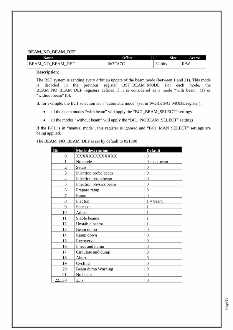
BEAM_NO_BEAM_DEF Name Offset Size Access
BEAM_NO_BEAM_DEF 0x7FA7C 32 bits R/W
Description:
The BST system is sending every orbit an update of the beam mode (between 1 and 21). This mode is decoded in the previous register BST_BEAM_MODE For each mode, the BEAM_NO_BEAM_DEF registers defines if it is considered as a mode “with beam” (1) or “without beam” (0).
If, for example, the BC1 selection is in “automatic mode” (set in WORKING_MODE register):
• all the beam modes “with beam” will apply the “BC1_BEAM_SELECT” settings
• all the modes “without beam” will apply the “BC1_NOBEAM_SELECT” settings
If the BC1 is in “manual mode”, this register is ignored and “BC1_MAN_SELECT” settings are being applied.
The BEAM_NO_BEAM_DEF is set by default to 0x1F00
Bit Mode description Default 0 XXXXXXXXXXXXX 0 1 No mode 0 = no beam 2 Setup 0 3 Injection probe beam 0 4 Injection setup beam 0 5 Injection physics beam 0 6 Prepare ramp 0 7 Ramp 0 8 Flat top 1 = beam 9 Squeeze 1
10 Adjust 1 11 Stable beams 1 12 Unstable beams 1 13 Beam dump 0 14 Ramp down 0 15 Recovery 0 16 Inject and dump 0 17 Circulate and dump 0 18 Abort 0 19 Cycling 0 20 Beam dump Warning 0 21 No beam 0
22...30 x...x 0
Page
17
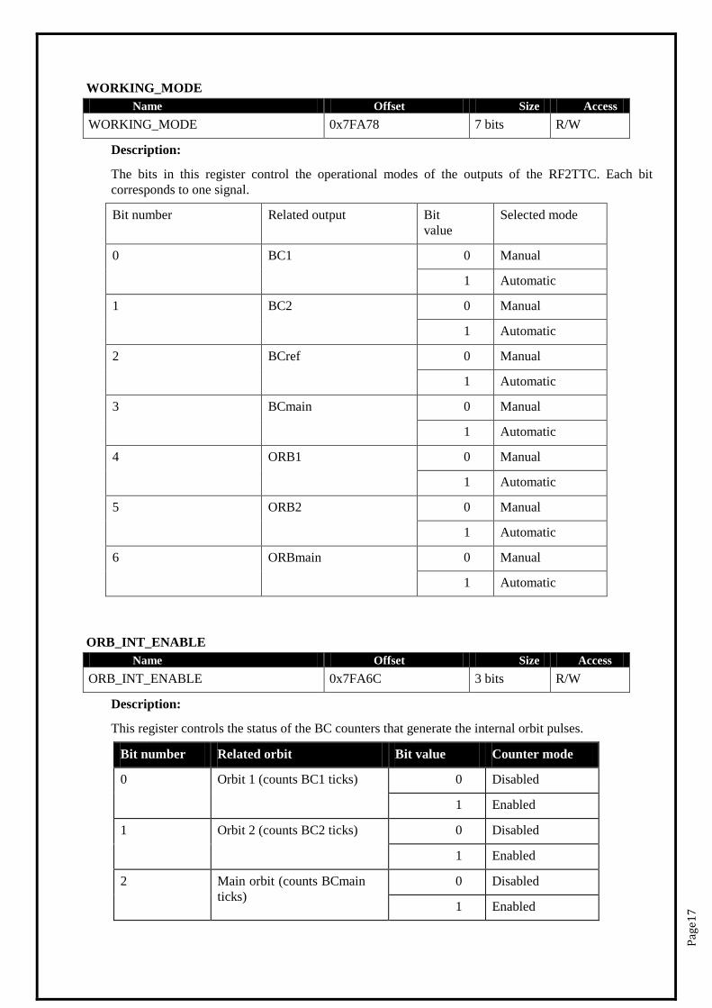
WORKING_MODE Name Offset Size Access
WORKING_MODE 0x7FA78 7 bits R/W
Description:
The bits in this register control the operational modes of the outputs of the RF2TTC. Each bit corresponds to one signal.
Bit number Related output Bit value
Selected mode
0 BC1 0 Manual
1 Automatic
1 BC2 0 Manual
1 Automatic
2 BCref 0 Manual
1 Automatic
3 BCmain 0 Manual
1 Automatic
4 ORB1 0 Manual
1 Automatic
5 ORB2 0 Manual
1 Automatic
6 ORBmain 0 Manual
1 Automatic
ORB_INT_ENABLE Name Offset Size Access
ORB_INT_ENABLE 0x7FA6C 3 bits R/W
Description:
This register controls the status of the BC counters that generate the internal orbit pulses.
Bit number Related orbit Bit value Counter mode
0 Orbit 1 (counts BC1 ticks) 0 Disabled
1 Enabled
1 Orbit 2 (counts BC2 ticks) 0 Disabled
1 Enabled
2 Main orbit (counts BCmain ticks)
0 Disabled
1 Enabled
Page
18
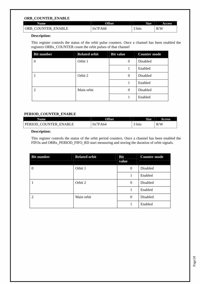
ORB_COUNTER_ENABLE Name Offset Size Access
ORB_COUNTER_ENABLE 0x7FA68 3 bits R/W
Description:
This register controls the status of the orbit pulse counters. Once a channel has been enabled the registers ORBx_COUNTER count the orbit pulses of that channel
Bit number Related orbit Bit value Counter mode
0 Orbit 1 0 Disabled
1 Enabled
1 Orbit 2 0 Disabled
1 Enabled
2 Main orbit 0 Disabled
1 Enabled
PERIOD_COUNTER_ENABLE Name Offset Size Access
PERIOD_COUNTER_ENABLE 0x7FA64 3 bits R/W
Description:
This register controls the status of the orbit period counters. Once a channel has been enabled the FIFOs and ORBx_PERIOD_FIFO_RD start measuring and storing the duration of orbit signals.
Bit number Related orbit Bit value
Counter mode
0 Orbit 1 0 Disabled
1 Enabled
1 Orbit 2 0 Disabled
1 Enabled
2 Main orbit 0 Disabled
1 Enabled
Page
19
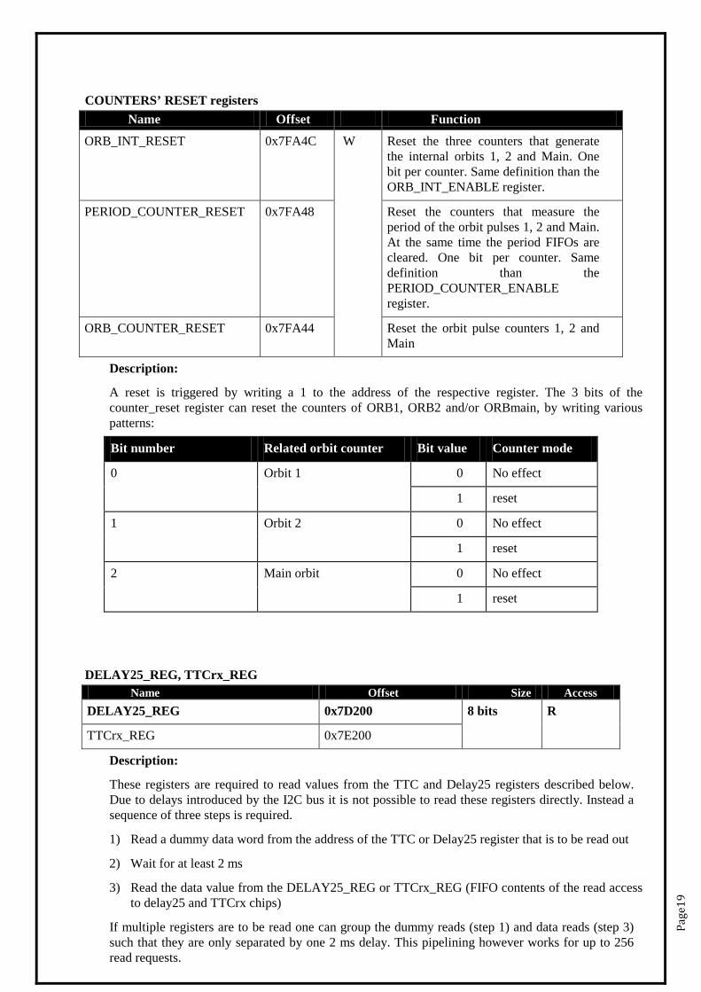
COUNTERS’ RESET registers Name Offset Function
ORB_INT_RESET 0x7FA4C W Reset the three counters that generate the internal orbits 1, 2 and Main. One bit per counter. Same definition than the ORB_INT_ENABLE register.
PERIOD_COUNTER_RESET 0x7FA48 Reset the counters that measure the period of the orbit pulses 1, 2 and Main. At the same time the period FIFOs are cleared. One bit per counter. Same definition than the PERIOD_COUNTER_ENABLE register.
ORB_COUNTER_RESET 0x7FA44 Reset the orbit pulse counters 1, 2 and Main
Description:
A reset is triggered by writing a 1 to the address of the respective register. The 3 bits of the counter_reset register can reset the counters of ORB1, ORB2 and/or ORBmain, by writing various patterns:
Bit number Related orbit counter Bit value Counter mode
0 Orbit 1 0 No effect
1 reset
1 Orbit 2 0 No effect
1 reset
2 Main orbit 0 No effect
1 reset
DELAY25_REG, TTCrx_REG Name Offset Size Access
DELAY25_REG 0x7D200 8 bits R
TTCrx_REG 0x7E200
Description:
These registers are required to read values from the TTC and Delay25 registers described below. Due to delays introduced by the I2C bus it is not possible to read these registers directly. Instead a sequence of three steps is required.
1) Read a dummy data word from the address of the TTC or Delay25 register that is to be read out
2) Wait for at least 2 ms
3) Read the data value from the DELAY25_REG or TTCrx_REG (FIFO contents of the read access to delay25 and TTCrx chips)
If multiple registers are to be read one can group the dummy reads (step 1) and data reads (step 3) such that they are only separated by one 2 ms delay. This pipelining however works for up to 256 read requests.
Page
20
BC_ DELAY25_x Name Offset Startup value Size Access
BC_DELAY25_GCR 0x7D014 0x00 8 bits (R)/W
BC_DELAY25_BCmain 0x7D00c 0x40
BC_DELAY25_BCref 0x7D008 0x40
BC_DELAY25_BC2 0x7D004 0x40
BC_DELAY25_BC1 0x7D000 0x40
Description:
These registers control the configuration of the Delay25 chips for the BC signals. These chips ensure the BC signal to be shifted by steps of 0.5ns with a jitter lower than 19ps rms. For details about the read protocol see above. Bit definition (from Delay25 manual):
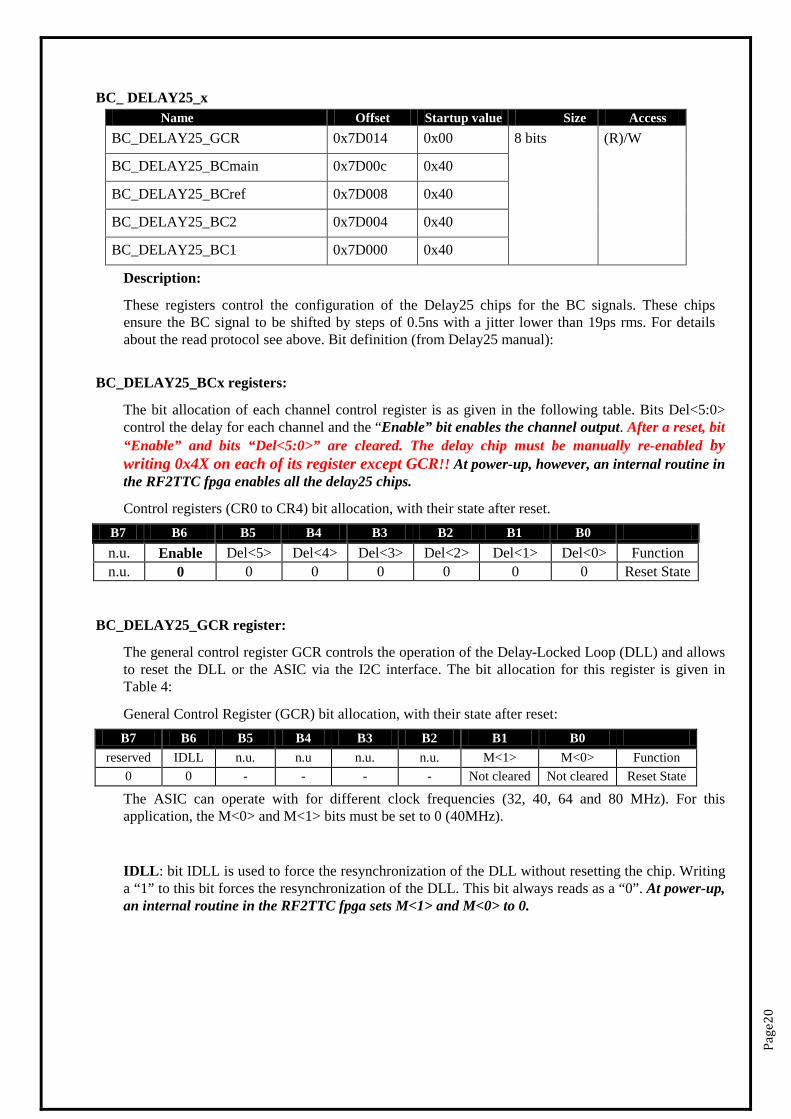
BC_DELAY25_BCx registers:
The bit allocation of each channel control register is as given in the following table. Bits Del<5:0> control the delay for each channel and the “Enable” bit enables the channel output. After a reset, bit “Enable” and bits “Del<5:0>” are cleared. The delay chip must be manually re-enabled by writing 0x4X on each of its register except GCR!! At power-up, however, an internal routine in the RF2TTC fpga enables all the delay25 chips.
Control registers (CR0 to CR4) bit allocation, with their state after reset. B7 B6 B5 B4 B3 B2 B1 B0 n.u. Enable Del<5> Del<4> Del<3> Del<2> Del<1> Del<0> Function n.u. 0 0 0 0 0 0 0 Reset State
BC_DELAY25_GCR register:
The general control register GCR controls the operation of the Delay-Locked Loop (DLL) and allows to reset the DLL or the ASIC via the I2C interface. The bit allocation for this register is given in Table 4:
General Control Register (GCR) bit allocation, with their state after reset: B7 B6 B5 B4 B3 B2 B1 B0
reserved IDLL n.u. n.u n.u. n.u. M<1> M<0> Function 0 0 - - - - Not cleared Not cleared Reset State
The ASIC can operate with for different clock frequencies (32, 40, 64 and 80 MHz). For this application, the M<0> and M<1> bits must be set to 0 (40MHz).
IDLL: bit IDLL is used to force the resynchronization of the DLL without resetting the chip. Writing a “1” to this bit forces the resynchronization of the DLL. This bit always reads as a “0”. At power-up, an internal routine in the RF2TTC fpga sets M<1> and M<0> to 0.
Page
21
ORBIN_DELAY25_x Name Offset Startup Value Size Access
ORBIN_DELAY25_GCR 0x7D034 0x00 8 bits (R)/W
ORBIN_DELAY25_ORB2 0x7D024 0x40
ORBIN_DELAY25_ORB1 0x7D020 0x40
Description:
These registers control the configuration of the Delay25 chips for the orbit input signals. Finely adjusting the delay of the orbit inputs (with steps of 0.5ns) allows moving the rising edge of the orbit pulse away from the rising edge of the corresponding bunch clock to ensure a good synchronisation of the 2 signals (basically to avoid the metastability generated if the rising edge of the orbit is in the setup time or hold time of the latch). The window in which the orbit will be stably synchronized is of the order of 20ns out of 25.
The way to choose the good value for these registers is described in 2.3 Calibration Procedures.
For details about the read protocol see above. Bit definition: see BC_DELAY_x register.
Note: After a reset, bit “Enable” and bits “Del<5:0>” are cleared. The delay chip must be manually re-enabled by writing 0x4X on each of its register except GCR!!
ORBOUT_DELAY25_x Name Offset Startup Value Size Access
ORBOUT_DELAY25_GCR 0x7D054 0x00 8 bits (R)/W
ORBOUT_DELAY25_ORBmain 0x7D048 0x40
ORBOUT_DELAY25_ORB2 0x7D044 0x40
ORBOUT_DELAY25_ORB1 0x7D040 0x40
Description:
These registers control the configuration of the Delay25 chips for the orbit output signals. This adjustment is to allow the experiments fine tuning the orbit for its use in their trigger electronics. For details about the read protocol see above. Bit definition: see BC_DELAY25_x register.
Note: After a reset, bit “Enable” and bits “Del<5:0>” are cleared. The delay chip must be manually re-enabled by writing 0x4X on each of its register except GCR!!
Page
22
TTCrx REGISTERS
Name Offset Size Access TTCrx_pointer to the register 0x7E000 8 bits R/W
TTCrx_pointer to the data 0x7E004 8 bits W
Description:
These are the two registers used to read and write all the internal registers of the TTCrx used to receive the BST message (see TTCrx user manual). Only one register requires to be accessed for the purpose of receiving the BST message: the control register (internal address= 0x03). Its value should be 0xB3 instead of 0x93 (its default value). The ‘1’ added on bit 5 allows enabling the Dout bus of the TTCrx, which contains the broadcast data, and hence the Machine Mode.
Register access protocol:
The TTCrx chip needs to be ready (ie, the optical fibre needs to deliver a correct encoded 40MHz clock), in order to access the internal registers.
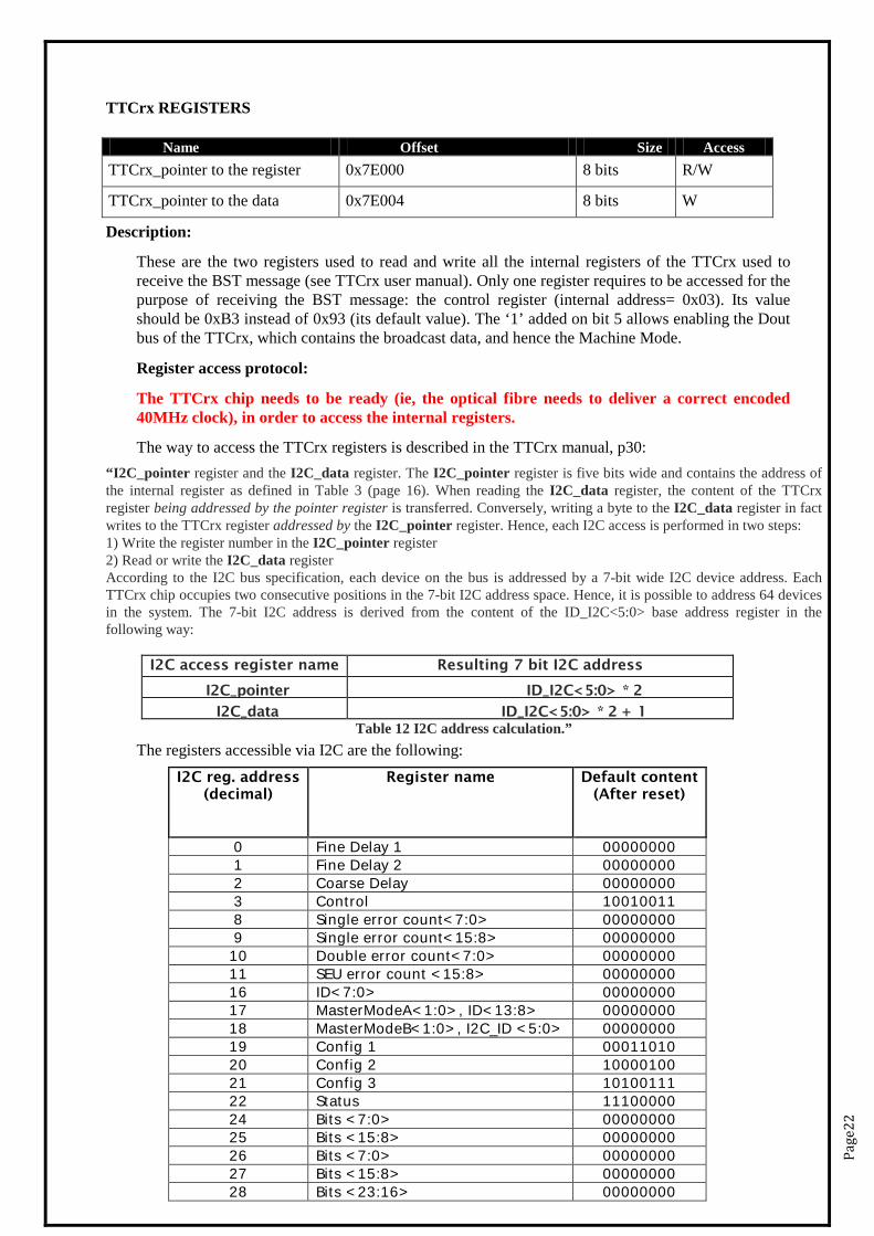
The way to access the TTCrx registers is described in the TTCrx manual, p30: “I2C_pointer register and the I2C_data register. The I2C_pointer register is five bits wide and contains the address of the internal register as defined in Table 3 (page 16). When reading the I2C_data register, the content of the TTCrx register being addressed by the pointer register is transferred. Conversely, writing a byte to the I2C_data register in fact writes to the TTCrx register addressed by the I2C_pointer register. Hence, each I2C access is performed in two steps: 1) Write the register number in the I2C_pointer register 2) Read or write the I2C_data register According to the I2C bus specification, each device on the bus is addressed by a 7-bit wide I2C device address. Each TTCrx chip occupies two consecutive positions in the 7-bit I2C address space. Hence, it is possible to address 64 devices in the system. The 7-bit I2C address is derived from the content of the ID_I2C<5:0> base address register in the following way:
I2C access register name Resulting 7 bit I2C address I2C_pointer ID_I2C<5:0> * 2
I2C_data ID_I2C<5:0> * 2 + 1 Table 12 I2C address calculation.”
The registers accessible via I2C are the following: I2C reg. address
(decimal) Register name Default content
(After reset)
0 Fine Delay 1 00000000 1 Fine Delay 2 00000000 2 Coarse Delay 00000000 3 Control 10010011 8 Single error count<7:0> 00000000 9 Single error count<15:8> 00000000 10 Double error count<7:0> 00000000 11 SEU error count <15:8> 00000000 16 ID<7:0> 00000000 17 MasterModeA<1:0>, ID<13:8> 00000000 18 MasterModeB<1:0>, I2C_ID <5:0> 00000000 19 Config 1 00011010 20 Config 2 10000100 21 Config 3 10100111 22 Status 11100000 24 Bits <7:0> 00000000 25 Bits <15:8> 00000000 26 Bits <7:0> 00000000 27 Bits <15:8> 00000000 28 Bits <23:16> 00000000
Page
23
Example of registers read and write via VME access:
1- VME WRITE, AM=0x09, RegOFFSET=0xE000, Data=0x3 (register I2C address)
Read control register (I2C address 3):
2- VME READ, AM=0x09, RegOFFSET=0xE000, (the Data read has no meaning)
3- VME READ, AM=0x09, RegOFFSET=0xE200, Data should be 0x000000FF after initialisation
1- VME WRITE, AM=0x09, RegOFFSET=0xE000, Data=0x1 (register I2C address)
Write Fine Delay Register (I2C address 1):
2- VME WRITE, AM=0x09, RegOFFSET=0xE004 (offset of the data register), 0x0000YOURDATA
1- VME WRITE, AM=0x09, RegOFFSET=0xE000, Data=0x1
Read fine delay register (I2C address 1):
2- VME READ, AM=0x09, RegOFFSET=0xE000, (the Data read has no meaning)
3- VME READ, AM=0x09, RegOFFSET=0xE200, Data should be 0x000XYOURDATA, with X=0 if the fIFO is not empty, X=1 if you are reading the last word stored in a FIFO
4- VME WRITE, AM=0x09, RegOFFSET=0xE000, Data=0x1
Successively read fine delay registers 1 and 2 (I2C address 1 and 2):
5- VME READ, AM=0x09, RegOFFSET=0xE000, (the Data read has no meaning)
6- VME WRITE, AM=0x09, RegOFFSET=0xE000, Data=0x2
7- VME READ, AM=0x09, RegOFFSET=0xE000, (the Data read has no meaning)
8- VME READ, AM=0x09, RegOFFSET=0xE200, Data should be 0x0000YOURDATA
9- VME READ, AM=0x09, RegOFFSET=0xE200, Data should be 0x0001YOURDATA

Page
24
2.3.
For a proper operation of the RF2TTC in its environment, a number of registers have to be tuned by the user (delays, thresholds, length). The purpose of adjusting the delay of the Bunch Clock outputs is easy to understand, as well as delaying the orbit output signals (finely with 0.5ns steps or coarsely with 25ns steps.
CALIBRATION PROCEDURES
However, finding the right values for the orbit_in delay and threshold registers is not so easy. The following calibration procedure may help you to optimize these settings.
2.3.1. The orbit is arriving at the board input as a 5ns sinusoidal pulse, with 1V amplitude on 50 Ohm termination. To be converted to a digital pulse, it is first compared to an adjustable threshold (set by the ORBx_DAC register), then stretched to 40ns, and then finally latched by one of the Bunch Clocks.
Threshold adjustment (ORBx_DAC)
The threshold is adjusted via the ORBx_DAC register, according to the formula:
Threshold = -1.25 + value * 2.5 / 255
The ORBx_DAC registers are set to 0xAA by default (which corresponds to 0.416V). This value should match perfectly with the level of the input signals. However, if you have any doubt or you want to adjust it better, we advise you to respect the following procedure. ‘x’ = ‘1’ or ‘2’.
1. Set your board to receive BCx and Orbx from a reliable external source (synchronised BC and Orbit, with orbit period= 3564BC)
2. Set the ORBx_DAC to 0
3. Reset the Orbx fifo
4. Read 100 times ORBx_PERIOD_FIFO_RD.
5. While ORBx_DAC < 0xFF, ORBx_DAC <= ORBx_DAC +1 and go back to 3),
6. You should get a window of threshold values of, for example, [0x09;0xF0], for which the 100 periods are all 2564 (0xDEC). Then pick-up one value in the middle of the range and set the ORBx_DAC with it.
ORBx_DAC= 0xFF= +1.25V
ORBx_DAC= 0x00= -1.25V
Orbit signal at the input of the board: 5ns sinusoidal pulse, 1Vpkpk on 50 Ohms ORBx_DAC= 0xAA= +0.416V
PECL Comparator
Output: 5ns PECL pulse
Stretcher AHC123
Output: 40 ns PECL pulse
Delay 25
ORB
IND
ELAY
25x
= 0
x00
(0ns
)
ORB
IND
ELAY
25x
= 0
x31(
24.5
ns)
Page
25
2.3.2. The ORBIN_DELAY25_ORBx are 2 registers configuring the Delay25 chips on orb1 and orb2 inputs. They are set to 0x40 by default, which means that they are enabled (bit6) with a delay of 0x00. The delay can go from 0 (=0ns) to 0x3F (31.5ns), by steps of 0.5ns.
Orbit inputs delay adjustment
As you can see on the diagram below, the orbit, once stretched to a 40ns pulse, is latched by its corresponding Bunch Clock:
• BC1 for orb1,
• BC2 for orb2, and
• BCmain for orbmain (with BCmain = BC1, BC2 or BCref).
We do not consider the case of internal bunch clocks, as it wouldn’t make much sense latching an external orbit with an internal (ie not synchronous) clock.
As the phase between the orbit and its relative BC is not known when it enters the latch in the FPGA, we may face a problem of metastability if the rising edge of the orbit pulse occurs close to the rising edge of the BC. This metastability window is in a range of [-setup time; +hold time] of internal FPGA flipflops, which should be of the order of max [-1ns;+1ns] (see graph below). Although very unlikely to happen, this situation must
be avoided, and a calibration is recommended.
Orb_in_delayed BC
1
2
3 4

Page
26
Thereby,
a) Orb1 must be calibrated to match BC1 (Dflipflop 1 on the diagram)
b) Orb2 must be calibrated to match BC2 (Dflipflop 2).
But it is not enough! You have also to ensure that your Orbmain is matching BCmain. The duo Orbmain/BCmain can be made of:
c) Orb1/BC1: Dflipflop3 (if Orbmain=Orb1 and BCmain=BC1), or
d) Orb1/BCref: Dflipflop3 (if Orbmain=Orb1 and BCmain=BCref), or
e) Orb2/BC2: Dflipflop4 (if Orbmain=Orb2 and BCmain=BC2), or
f) Orb2/BCref: Dflipflop4 (if Orbmain=Orb2 and BCmain=BCref), or
Note that, if c) and e) look similar to a) and b), the flipflop is different and the clock is following another path, so the phase between Orb and BC may be different.
A minimal calibration procedure would include at least 3 of the above points.
• The two first ones, a) and b), are mandatory
• The, according to the choice you made for the orbmain/bcmain, you have to pick-up one of the 4 :c) or d) or e) or f). If you plan to use several configurations, you have to calibrate for example c) AND d). This is not a problem, as the working window is very large. To be conservative, you may do the 6 cycles of calibration (3 per orbit input), and you will be sure they will always be safely latched.
The calibration procedure is similar to the threshold adjustment described above:
1. Connect your board to the RF_Rx modules outputs
2. Adjust the phase of the clocks (BC1, BC2, BCref and BCmain) according to your detector requirements. (use the BCdelay25 registers).
3. ORB1_out: Calibrate case a) (mandatory):
a. Set your board to have BC1_MAN_SELECT=ext and ORB1_MAN_SELECT=external
b. Set ORBIN_DELAY25_ORB1 to 0x40 (enabled, 0 delay)
c. Reset the Orb fifo (PERIOD_COUNTER_RESET)
d. Read 256 times ORB1_PERIOD_FIFO_RD (a complete fifo until it is empty).
e. While ORBIN_DELAY25_ORB1[5,0] < 0x40, ORBIN_DELAY25_ORB1++ and go back to c), Pay attention to keep the ORBIN_DELAY25_ORB1[6]=1 (chip enabled).
f. You should get a window (called here Orb1_Wa) of about 40 consecutive steps for which the 256 periods are all 2564 (0xDEC).
Page
27
4. ORB2_out: Calibrate case b)
a. Set your board to have BC2_MAN_SELECT=ext and ORB2_MAN_SELECT=external
b. Set ORBIN_DELAY25_ORB2 to 0x40 (enabled, 0 delay)
c. Reset the Orb fifo (PERIOD_COUNTER_RESET)
d. Read 256 times ORB2_PERIOD_FIFO_RD (a complete fifo until it is empty).
e. While ORBIN_DELAY25_ORB2[5,0] < 0x40, ORBIN_DELAY25_ORB2++ and go back to c),
f. You should get a window (called here Orb2_Wb) of about 40 consecutive steps for which the 256 periods are all 2564 (0xDEC).
5. ORBmain_out: Calibrate case c) or/and d) or/and e) or/and f). Example of case c) below:
a. Set your board to have BCmain_MAN_SELECT=BC1 and ORBmain_MAN_SELECT=ORB1
b. Set ORBIN_DELAY25_ORB1 to 0x40 (enabled, 0 delay)
c. Reset the Orb fifo (PERIOD_COUNTER_RESET)
d. Read 256 times ORBmain_PERIOD_FIFO_RD (a complete fifo until it is empty).
e. While ORBIN_DELAY25_ORB1[5,0] < 0x40, ORBIN_DELAY25_ORB1++ and go back to c),
f. You should get a window (called here Orb1_Wc) of about 40 consecutive steps for which the 256 periods are all 2564 (0xDEC).
g. Do the same procedure for d, e and f. You will get Orb1_Wd, Orb2_We and Orb2_Wf.
6. Finally, find the best match:
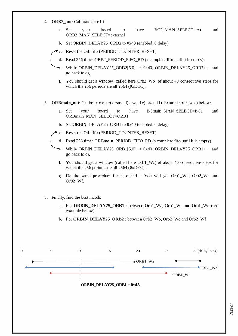
a. For ORBIN_DELAY25_ORB1 : between Orb1_Wa, Orb1_Wc and Orb1_Wd (see example below)
b. For ORBIN_DELAY25_ORB2 : between Orb2_Wb, Orb2_We and Orb2_Wf
0 5 10 15 20 25 30(delay in ns)
ORB1_Wa
ORB1_Wc
ORB1_Wd
ORBIN_DELAY25_ORB1 = 0x4A

Page
28
2.4.
FIBRE / CABLE CONNECTIONS
Connector name To be connected to
BST TTC encoded signal.
One of the BST optical fibres (two are normally available, one per ring). The optical power level should be between -5dBm and -25dBm.
BC INPUTS – BC1 ECL AC coupled signal.
Should be connected to the BC1 output of the RF_Rx_D
BC INPUTS – BC2 ECL AC coupled signal.
Should be connected to the BC2 output of the RF_Rx_D
BC INPUTS – BC_REF ECL AC coupled signal.
Should be connected to the BCref output of the RF_Rx_D
ORB INPUTS – ORB1 ECL AC coupled signal.
Should be connected to the ORB1 output of the RF_Rx_D
ORB INPUTS – ORB2 ECL AC coupled signal.
Should be connected to the ORB2 output of the RF_Rx_D
BC OUTPUTS – BC1 • ECL AC coupled signal.
• a NIM copy is also available (for oscilloscope monitoring for example).
BC OUTPUTS – BC2 • ECL AC coupled signal.
• a NIM copy is also available
BC OUTPUTS – BC_REF • ECL AC coupled signal.
• a NIM copy is also available
BC OUTPUTS – BCmain • ECL AC coupled signal.
• a NIM copy is also available
ORB OUTPUTS – ORB1 • ECL AC coupled signal.
• a NIM copy is also available
ORB OUTPUTS – ORB2 • ECL AC coupled signal.
• a NIM copy is also available
ORB OUTPUTS – ORBmain
• ECL AC coupled signal.
• a NIM copy is also available

Page
29
2.5.
The typical outputs ECL amplitude that we have after 2m of cables on 50Ohm terminated ends are:
OUTPUT SIGNAL AMPLITUDE INFORMATION
o BC: 670mV amplitude
o POSITIVE ORBIT: 1.1V
o NEGATIVE ORBIT: 570mV These values have been set to fit the various needs of all the users, but could need to be adjusted for a special need (ex: increase the negative orbit amplitude). It is possible to increase or decrease all these amplitudes just by changing the value of one resistor per output. Please contact Stephane DETRAZ or Sophie BARON if you want to do it.
2.6.
FRONT-PANEL LEDS
LED Description
BC1_LOCK Displays the state of the QPLL chip connected to the selected BC1 signal. (ON=locked/OFF=not locked).
BC2_LOCK Displays the state of the QPLL chip connected to the selected BC1 signal. (ON=locked/OFF=not locked).
BCREF_LOCK Displays the state of the QPLL chip connected to the selected BC1 signal. (ON=locked/OFF=not locked).
BCmain_LOCK Displays the state of the QPLL chip connected to the selected BC1 signal. (ON=locked/OFF=not locked).
ORB1_OK Monitors the presence of the external orbit after the comparator. (ON=signal present, OFF= no signal). When OFF, it can mean, either that the orbit is not present, or that the DAC setting the threshold at the input does not deliver an adapted threshold.
ORB2_OK Monitors the presence of the external orbit after the comparator. (ON=signal present, OFF= no signal). When OFF, it can mean, either that the orbit is not present, or that the DAC setting the threshold at the input does not deliver an adapted threshold.
BEAM Monitors if the current machine mode corresponds to a “BEAM” mode or a “NO BEAM” mode. (ON=BEAM/OFF=NO BEAM).
BST ready Monitors the state of the TTCrx in charge of receiving and transmitting the BST message to the FPGA. (ON=TTCrx ready, received frame is consistent and can be decoded/ OFF=no consistent BST message).
BERR Flashes when the RF2TTC generates a BERR. Not implemented yet.
VME Flashes if the RF2TTC has replied to a VMEbus cycle

Page
30
2.7.
2.7.1.
IMPROVEMENTS MADE ON THE PRODUCTION VERSION ( V3)
The state of the Delay25 chips after a power-up was not satisfactory, as the outputs were all disabled. The same for the TTCrx, which does not allow by default the transmission of the broadcast words. Finally, the DAC in charge of the threshold adjustments are set to -1.25V by default after power-up. Hence, the Delay25, TTCrx and DAC chips need to be initialised first, and it requires using some internal protocols (I2C or other), controlled by VME accesses.
Initialisation procedure
A solution was provided to ensure the board initialisation (after power up, sys reset or reconfiguration) without using a crate processor. This initialisation ensures that:
• All the delay25 chips are enabled (i.e. transmit the signals present at their inputs) (0x40 is written in all of their delay registers)
• All the DACs are configured correctly to allow latching the input orbits if any (set to 0xAA)
• The TTCrx chips is configured to transmit the BST message to the FPGA (control register is set to 0xFF)
• All the signals are set to INTERNAL by default

Page
31
2.8.
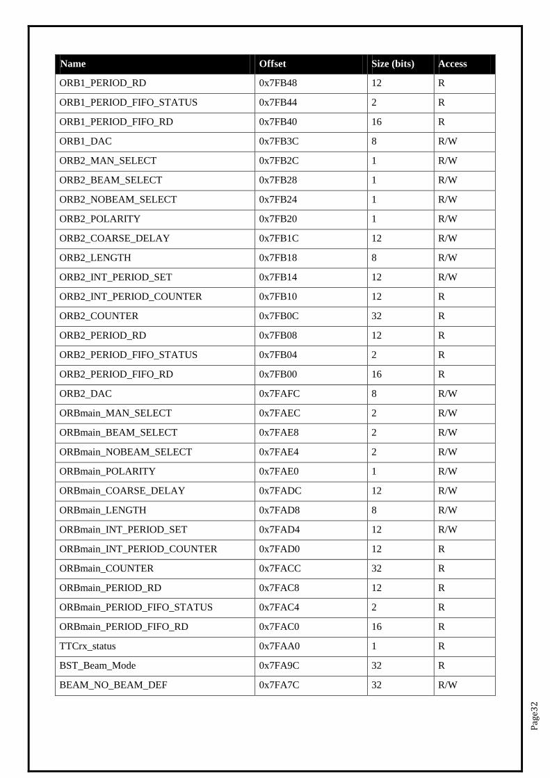
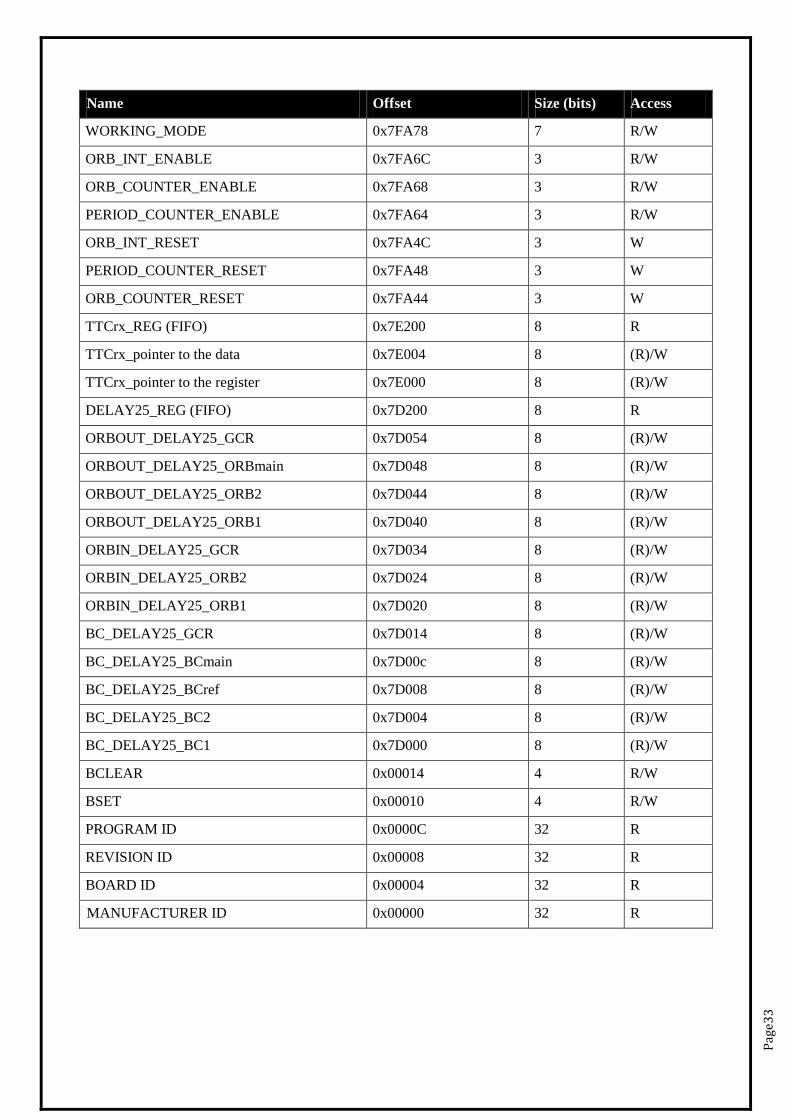
Name
REGISTERS SUMMARY
Offset Size (bits) Access
BC1_MAN_SELECT 0x7FBFC 1 R/W
BC1_BEAM_SELECT 0x7FBF8 1 R/W
BC1_NOBEAM_SELECT 0x7FBF4 1 R/W
BC1_QPLL_MODE 0x7FBF0 1 R/W
BC1_DAC 0x7FBEC 8 R/W
BC1_QPLL_STATUS 0x7FBE8 2 R
BC2_MAN_SELECT 0x7FBCC 1 R/W
BC2_BEAM_SELECT 0x7FBC8 1 R/W
BC2_NOBEAM_SELECT 0x7FBC4 1 R/W
BC2_QPLL_MODE 0x7FBC0 1 R/W
BC2_DAC 0x7FBBC 8 R/W
BC2_QPLL_STATUS 0x7FBB8 2 R
BCref_MAN_SELECT 0x7FBAC 1 R/W
BCref_BEAM_SELECT 0x7FBA8 1 R/W
BCref_NOBEAM_SELECT 0x7FBA4 1 R/W
BCref_QPLL_MODE 0x7FBA0 1 R/W
BCref_DAC 0x7FB9C 8 R/W
BCref_QPLL_STATUS 0x7FB98 2 R
BCmain_MAN_SELECT 0x7FB8C 2 R/W
BCmain_BEAM_SELECT 0x7FB88 2 R/W
BCmain_NOBEAM_SELECT 0x7FB84 2 R/W
BCmain_QPLL_MODE 0x7FB80 1 R/W
BCmain_QPLL_STATUS 0x7FB7C 2 R/W
ORB1_MAN_SELECT 0x7FB6C 1 R/W
ORB1_BEAM_SELECT 0x7FB68 1 R/W
ORB1_NOBEAM_SELECT 0x7FB64 1 R/W
ORB1_POLARITY 0x7FB60 1 R/W
ORB1_COARSE_DELAY 0x7FB5C 12 R/W
ORB1_LENGTH 0x7FB58 8 R/W
ORB1_INT_PERIOD_SET 0x7FB54 12 R/W
ORB1_INT_PERIOD_COUNTER 0x7FB50 12 R
ORB1_COUNTER 0x7FB4C 32 R
Page
32
Name Offset Size (bits) Access
ORB1_PERIOD_RD 0x7FB48 12 R
ORB1_PERIOD_FIFO_STATUS 0x7FB44 2 R
ORB1_PERIOD_FIFO_RD 0x7FB40 16 R
ORB1_DAC 0x7FB3C 8 R/W
ORB2_MAN_SELECT 0x7FB2C 1 R/W
ORB2_BEAM_SELECT 0x7FB28 1 R/W
ORB2_NOBEAM_SELECT 0x7FB24 1 R/W
ORB2_POLARITY 0x7FB20 1 R/W
ORB2_COARSE_DELAY 0x7FB1C 12 R/W
ORB2_LENGTH 0x7FB18 8 R/W
ORB2_INT_PERIOD_SET 0x7FB14 12 R/W
ORB2_INT_PERIOD_COUNTER 0x7FB10 12 R
ORB2_COUNTER 0x7FB0C 32 R
ORB2_PERIOD_RD 0x7FB08 12 R
ORB2_PERIOD_FIFO_STATUS 0x7FB04 2 R
ORB2_PERIOD_FIFO_RD 0x7FB00 16 R
ORB2_DAC 0x7FAFC 8 R/W
ORBmain_MAN_SELECT 0x7FAEC 2 R/W
ORBmain_BEAM_SELECT 0x7FAE8 2 R/W
ORBmain_NOBEAM_SELECT 0x7FAE4 2 R/W
ORBmain_POLARITY 0x7FAE0 1 R/W
ORBmain_COARSE_DELAY 0x7FADC 12 R/W
ORBmain_LENGTH 0x7FAD8 8 R/W
ORBmain_INT_PERIOD_SET 0x7FAD4 12 R/W
ORBmain_INT_PERIOD_COUNTER 0x7FAD0 12 R
ORBmain_COUNTER 0x7FACC 32 R
ORBmain_PERIOD_RD 0x7FAC8 12 R
ORBmain_PERIOD_FIFO_STATUS 0x7FAC4 2 R
ORBmain_PERIOD_FIFO_RD 0x7FAC0 16 R
TTCrx_status 0x7FAA0 1 R
BST_Beam_Mode 0x7FA9C 32 R
BEAM_NO_BEAM_DEF 0x7FA7C 32 R/W
Page
33
Name Offset Size (bits) Access
WORKING_MODE 0x7FA78 7 R/W
ORB_INT_ENABLE 0x7FA6C 3 R/W
ORB_COUNTER_ENABLE 0x7FA68 3 R/W
PERIOD_COUNTER_ENABLE 0x7FA64 3 R/W
ORB_INT_RESET 0x7FA4C 3 W
PERIOD_COUNTER_RESET 0x7FA48 3 W
ORB_COUNTER_RESET 0x7FA44 3 W
TTCrx_REG (FIFO) 0x7E200 8 R
TTCrx_pointer to the data 0x7E004 8 (R)/W
TTCrx_pointer to the register 0x7E000 8 (R)/W
DELAY25_REG (FIFO) 0x7D200 8 R
ORBOUT_DELAY25_GCR 0x7D054 8 (R)/W
ORBOUT_DELAY25_ORBmain 0x7D048 8 (R)/W
ORBOUT_DELAY25_ORB2 0x7D044 8 (R)/W
ORBOUT_DELAY25_ORB1 0x7D040 8 (R)/W
ORBIN_DELAY25_GCR 0x7D034 8 (R)/W
ORBIN_DELAY25_ORB2 0x7D024 8 (R)/W
ORBIN_DELAY25_ORB1 0x7D020 8 (R)/W
BC_DELAY25_GCR 0x7D014 8 (R)/W
BC_DELAY25_BCmain 0x7D00c 8 (R)/W
BC_DELAY25_BCref 0x7D008 8 (R)/W
BC_DELAY25_BC2 0x7D004 8 (R)/W
BC_DELAY25_BC1 0x7D000 8 (R)/W
BCLEAR 0x00014 4 R/W
BSET 0x00010 4 R/W
PROGRAM ID 0x0000C 32 R
REVISION ID 0x00008 32 R
BOARD ID 0x00004 32 R
MANUFACTURER ID 0x00000 32 R
Page
34
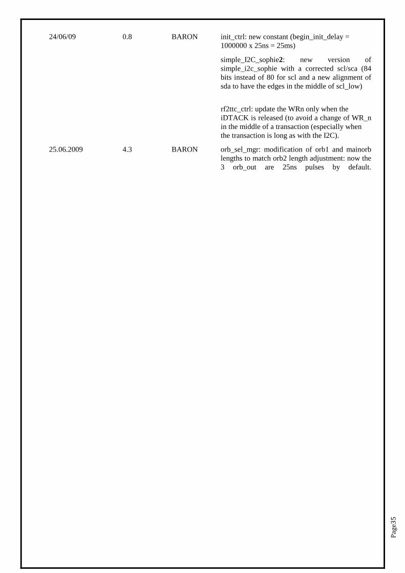
3.
LIST OF FIRMWARE UPDATES
DATE VERSION AUTHOR DESCRIPTION
03/10/06 0.01 BARON first VHDL entity definition clock selection feature
27.02.07 0.1 BARON remove CR/CSR space and use only User space
19.04.2007 inversion of orb int/ext encoding in register to be like BC
26.04.2007 BARON initial value for DAC=AA. Initial value for TTCrx control register is 0xff
30.04.07 BARON V3 of the hardware => Manual LSB and MSB addresses are inverted
08.05.07 BARON signal tap removed after timing pbs with the delay25 read back data_o latched by clock in simple_I2C (was not sync before)
29.10.2007 BARON modif to have consistency between orbit period register, real orbit period and measured orbit period
08.09.2008 BARON modif of the BST decoding to follow the 2 bytes of machine modes according to LHC-OP-ES- 0005 v.1.0 (bytes 26 and 27 - previously only 27.
13.09.2008 BARON compilation of files from may 08 for real time orbit reading and improvement of orbit length & delay
16.09.2008 0.2 BARON modification of machine_mode_mgr: to have a latching of the Beam Mode register only after the 2 bytes have been transmitted to the TTCrx. Adding of the orbit reading modification to allow a real time reading and storage in the FIFO, plus an improvement of orbit length and delay
08.10.2008 0.3 BARON correction on orb_sel_mgr: on period_fifo_wr_ena, modif per_fifo_status reg to memorize every full/empty until next read
14.01.2009 0.4 BARON modif on 'mach_mode-mgr': on mmode_decode_process to sync it with clock40des1 instead of clock
19.01.2009 0.5 BARON modif on QPLL_mgr: the qpll status registers keeps unlock and error active until next read action of the register
13.02.2009 0.6 BARON modif on Orb_sel_mgr: following a request from Markus, the empty status given by a per_fifo_rd is now latched only when rdreq is active, to ensure that reading 0x4XXX means that the fifo is really empty! Previously, it meant that last word was being read. not very practical!
19.05.2009 0.7 BARON changes the definition of BSET and BCLEAR registers to allow individual reset of QPLL chips (bits 5..3). Change on the reset_n of the qpll registers (previously reset by qpll_reset. now by the general reset.
Page
35
24/06/09 0.8 BARON init_ctrl: new constant (begin_init_delay = 1000000 x 25ns = 25ms)
simple_I2C_sophie2: new version of simple_i2c_sophie with a corrected scl/sca (84 bits instead of 80 for scl and a new alignment of sda to have the edges in the middle of scl_low)
rf2ttc_ctrl: update the WRn only when the iDTACK is released (to avoid a change of WR_n in the middle of a transaction (especially when the transaction is long as with the I2C).
25.06.2009 4.3 BARON orb_sel_mgr: modification of orb1 and mainorb lengths to match orb2 length adjustment: now the 3 orb_out are 25ns pulses by default.
Page
36
4.
4.1.
RF2TTC COMMON SOFTWARE
Even though the RF2TTC performs the same task in each of the four LHC experiments it will be operated in H/W and S/W environments that are specific to the respective experiment. Therefore the common S/W is limited to the lowest level which consists of some diagnostic programs and a user library. This S/W is implemented in the rf2ttc package and can be found in CERN CVS repository at
INTRODUCTION
http://isscvs.cern.ch/cgi-bin/viewcvs-all.cgi/rf2ttc/?cvsroot=rf2ttc. For direct access from Unix use (e.g.) “setenv CVSROOT :kserver:isscvs.cern.ch:/local/reps/rf2ttc”
4.1.1. In the ATLAS and ALICE experiments the RF2TTC is controlled by a VMEbus SBC from Concurrent Technologies (either a VP110 or a VP315). CMS uses a PCI-VMEbus link from CAEN and LHCb a USB-VMEbus link from the same manufacturer. In all four experiments the crate that houses the RF2TTC should be VME64X compatible as otherwise it is not possible use geographical addressing.
H/W Environment
4.1.2. On the low end ATLAS and ALICE will use the vme_rcc driver developed by ATLAS to communicate with the RF2TTC. CMS and LHCb will use S/W packages provided by CAEN for the respective interface. The common S/W will be programmed in a way that it is compatible with any of these bus access packages.
S/W Environment
At the top end each experiment has to develop appropriate secondary libraries and applications to interface the RF2TTC to their respective control systems. The development of the interface to the DIP server is also up to the experiments.
4.2.
Currently there exists one program that comes in three flavours: rf2ttcscope_atlice (for ATLAS and ALICE), rf2ttsscope_cms and rf2ttcscope_lhcb. This interactive application can be used to read, decode and write any register of the RF2TTC in a (hopefully) intuitive way. If a users feels that some functionality is lacking he is welcome to contact the developer (M. Joos). It is e.g. possible to extend rf2ttcscope by additional command line parameters such that certain tests can be executed from scripts.
TEST PROGRAMS
A tcltk graphical user interface (rf2ttc.tcl) is also available for test purpose. It has been written for SBCs from Concurrent Technologies (VP110 and VP315).
4.3.
This library consists of a common source file that implements the access to the registers of the RF2TTC in a generic way and a number of files to implement glue layers to the VMEbus access libraries from ATLAS and CAEN respectively.
THE USER LIBRARY