Class: ECE 7366 “Advanced Process Integration” Instructor: Dr. W. Zagozdzon-Wosik.
39
Class: ECE 7366 “Advanced Process Integration” Instructor: Dr. W. Zagozdzon-Wosik
-
Upload
doris-mccarthy -
Category
Documents
-
view
245 -
download
12
Transcript of Class: ECE 7366 “Advanced Process Integration” Instructor: Dr. W. Zagozdzon-Wosik.

Class: ECE 7366 “Advanced Process
Integration”Instructor: Dr. W. Zagozdzon-Wosik

INTRODUCTION
• This course is about the requirements for silicon chip fabrication and the technologies used to meet to thee specific needs of MOS and bipolar devices for current and future generations of ICs. Integration of the current processes and new processes/materials for further scaled down devices will be covered.• We will place a special emphasis on computer simulation tools to help understand these processes and as design tools. • These simulation tools are more sophisticated in some technology areas than in others, but in all areas they have made tremendous progress in recent years.
• 1960 and 1990 integrated circuits. • Progress due to: Feature size reduction - 0.7X/3 years (Moore’s Law).
Increasing chip size - ≈ 16% per year. “Creativity” in implementing functions.

Evolution of the Silicon Integrated Circuits since 1960s
Increasing: circuit complexity, packing density, chip size, speed, and reliability
Decreasing: feature size, price per bit, power (delay) product
1960s1990s

G. Marcyk

• The era of “easy” scaling is over. We are now in a period where technology and device innovations are required. Beyond 2020, new currently unknown inventions will be required.
Cell dimensions
Atomic dimensions
Device Scaling Over Time
0.1nm
1nm
10nm
1µm
10µm
100µm
1960 1980 2000 2020 2040
Transition Region
Quantum Effects Dominate
Atomic Dimensions
Feature Size
Year
0.1µm130 nm in 2002
18 nm in 2018
Era of Simple Scaling
Scaling + Innovation(ITRS)
Invention
~16% increase in complexity each year (now:6.3% for µP, 12% for DRAM)
~13% decrease in feature size each year (now: ~10%)
0.25µm in 1997

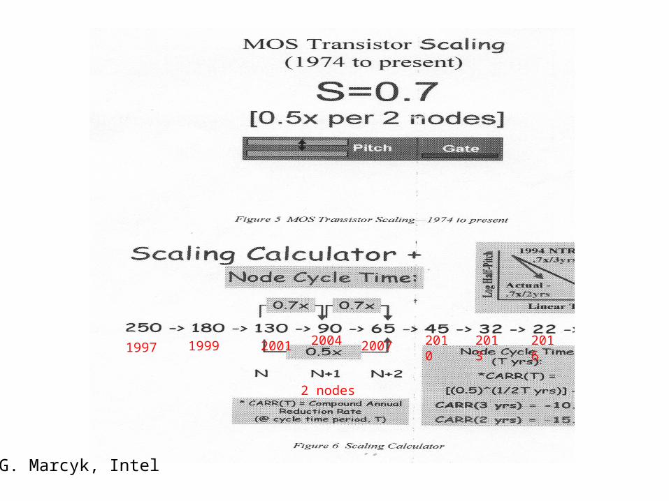
G. Marcyk, Intel
1997 1999 2001 2004 2007 2010
2013
2016
2 nodes


Trends in ScalingSi Microeletronics and MEMS

• 1990 IBM demo of Å scale “lithography”. • Technology appears to be capable of making structures much smaller than currently known device limits.
Year of Production 1998 2000 2002 2004 2007 2010 2013 2016 2018
Technology Node (half pitch) 250 nm 180 nm 130 nm 90 nm 65 nm 45 nm 32 nm 22 nm 18 nm
MPU Printed Gate Length 100 nm 70 nm 53 nm 35 nm 25 nm 18 nm 13 nm 10 nm
DRAM Bits/Chip (Sampling) 256M 512M 1G 4G 16G 32G 64G 128G 128G
MPU Transistors/Chip (x106) 550 1100 2200 4400 8800 14,000
Min Supply Voltage (volts) 1.8-2.5 1.5-1.8 1.2-1.5 0.9-1.2 0.8-1.1 0.7-1-0 06-0.9 0.5-0.8 0.5-0.7
ITRS at http://public.itrs.net/ (2003 version + 2004 update) – on class website.
• Assumes that CMOS technology dominates over the entire roadmap.• 2 year cycle moving to 3 years (scaling + innovation now required).
Trends in Increasing Integration Scale of CircuitsPast, Present, and Future ICs
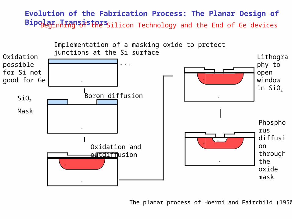
Evolution of the Fabrication Process: The Planar Design of Bipolar Transistors
Implementation of a masking oxide to protect junctions at the Si surface
Boron diffusionSiO2
Mask
Oxidation possible for Si not good for Ge
Oxidation and outdiffusion
Lithography to open window in SiO2
Phosphorus diffusion through the oxide mask
Beginning of the Silicon Technology and the End of Ge devices
P
N
N
N
P
N
Si O 2
N
P
N
The planar process of Hoerni and Fairchild (1950s)

Photolithography used for Pattern Formation
Beginning of Integrated Circuits in 1959Kilby (TI) and Noyce (Fairchild Semiconductors)
Substrate
Film deposition Photoresist application
Deposited Film Photoresist
Exposure
Development Etching Resist removal
Mask
Etch mask
Light
• Basic lithography process which is central to today’s chip fabrication.
• Sensitive to light• Durable in etching

Alignment of Layers to Fabricate IC Elements
Emitter
Collector
Resistor
P N
N
PNP BaseResistor
• Lithographic process allows integration of multiple devices side by side on a wafer.
• Bipolar Transistor and resistors made in the base region
•Accuracy of placement ~1/4 to 1/3 of the linewidth being printed
Vcc
C
B
E
BJT
0V
Contact to collector
R=L/W•Rs

Schematic Cross-Section of Modern CMOS Integrated Circuit with Two Metal Levels
IC is located at the surface of a Si wafer (~500µm thick)
P
P WellN Well
PNP+ P+ N+ N+PMOS NMOS
Via
Interconnect
SilicideOxide Isolation
M1
M2
OXIDE
TiN

Modern IC with a Five Level Metallization Scheme.
Planarization

• Actual cross-section of a modern microprocessor chip. Note the multiple levels of metal and planarization. (Intel website).
Computer Simulation Tools (TCAD)
•Most of the basic technologies in silicon chip manufacturing can now be simulated.Simulation is now used for:
• Designing new processes and devices.• Exploring the limits of semiconductor devices and
technology (R&D).• “Centering” manufacturing processes.• Solving manufacturing problems (what-if?)
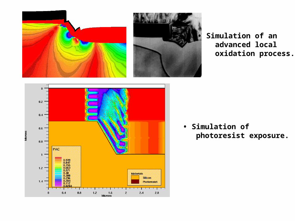
• Simulation of an advanced local oxidation process.
• Simulation of photoresist exposure.

Semiconductor Devices
Reverse biased diode
Forward biased diode
p-n Diodes
after Kano, Sem. Dev.
n+ for low resistance

p-n Diodes at Thermal Equilibrium
Uncompensated acceptors and donors
At thermal equilibrium charge neutrality qN+
dxn=qN-Axp leads to asymmetrical depletion layers
Electric field only in the depletion layer

Breakdown of a p-n Diode
Zener effect Avalanche effect
after Kano and Streetman

Breakdown Voltage of a p-n Diode
after Kano and Streetman
Eg
5-7V
• Ebr field increases with ND but not very much• Wdepl~1/√NDVbr=Ebr•Wdepl so Vbr decreases with ND

Transistors for digital and analg applications
MOSFET and Bipolar Junction Transistors

Bipolar Transistors
E-B junction is forward biased=injects minority carriers to the baseBase (electrically neutral) is responsible for electron transport via diffusion (or drift also if the build in electric field exist) to collectorC-B diode is reverse biased and collects transported carries
VBE>0 VBC<0
IE=IEn+IEp IC=IE<1
IB=IEp+Irec
IE IC
IB
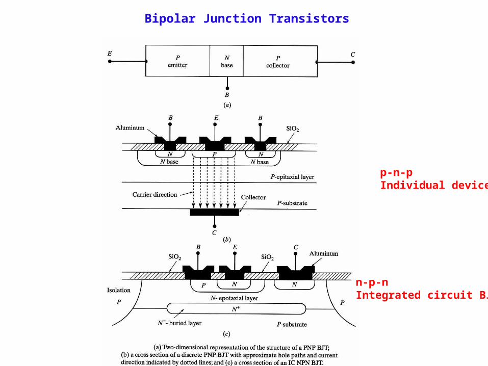
Bipolar Junction Transistors
n-p-nIntegrated circuit BJT
p-n-p Individual device

Bipolar Junction Transistors
minority carriers
Injectedelectrons
Extracted electronsholes
Forwards bias Reverse bias

Bipolar Junction Transistors
Forward Operation Mode
Early Effect
Early Voltage

Bipolar Junction Transistors
Breakdown Voltages
Common BaseCommon Emitter
Collector-Base junction

Bipolar Junction Transistors
Current Gain =
Gummel Plot
Kirk Effect
Recombination in the E-B SCR
IC/IB
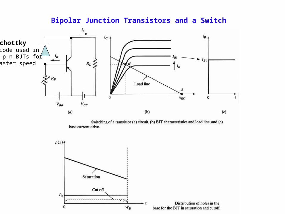
Bipolar Junction Transistors and a Switch
SchottkyDiode used in n-p-n BJTs forfaster speed

MOS Field Effect Transistors (MOSFET)
NMOS and PMOS (used in CMOS circuits)
VG>VT to create strong inversion
depletion
Oxide

Operation of NMOS-FET
Linear Region, Low VD
Saturation Region, Channel Starts to Pinch-Off
Saturation Region, channel shortens beyond pinch-off, L’<L
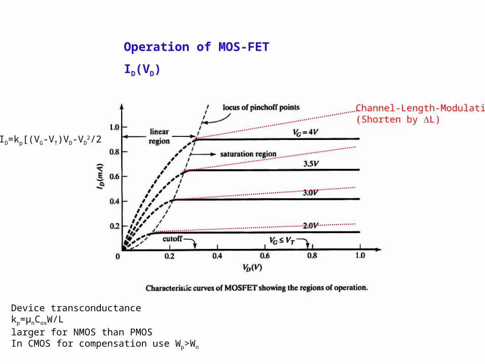
Operation of MOS-FET
ID(VD)
Channel-Length-Modulation(Shorten by L)
ID=kp[(VG-VT)VD-VD2/2
Device transconductancekp=µnCoxW/L larger for NMOS than PMOSIn CMOS for compensation use Wp>Wn

Scaled Down NMOS
DIBL
Proximity of the drain depletion layer charge sharing DIBL

Modern MOS Transistors
Gate
LDDLDD used to reduce the electric field in the drain depletion region and hot carrier effects
Self aligned contacts decrease the resistance
isolation
Drain
Source
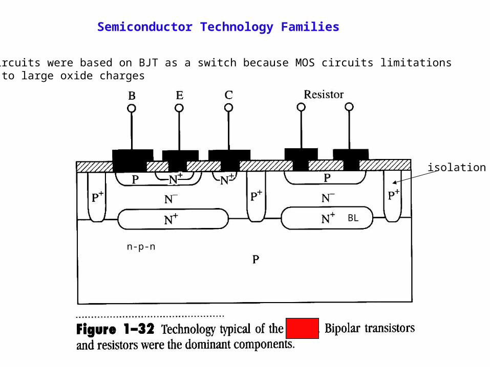
Semiconductor Technology Families
First circuits were based on BJT as a switch because MOS circuits limitations related to large oxide charges
isolation
BL
n-p-n

NMOS and CMOS Technologies
Enhancement NMOS Depletion NMOS
1970s
NMOS PMOS1980s and beyond Smaller power consumption

Challenges For The Future• Having a “roadmap” suggests that the future is well defined and there are few challenges to making it happen.
• The truth is that there are enormous technical hurdles to actually achieving the forecasts of the roadmap. Scaling is no longer enough.
• 3 stages for future development:
Materials/process innovationsNOW
Device innovationsIN 5-15 YEARS
Beyond Si CMOSIN 15 YEARS??
“Technology Performance Boosters” InventionSilicide
PolyGate
Substrate
Silicide
SidewallSpacer
RchanSource Drain
S/D Ext S/D Ext
GateDielectric
???
Gate
Source Drain• Spin-based devices • Molecular devices• Rapid single flux quantum• Quantum cellular automata• Resonant tunneling devices• Single electron devices
Plummer et al.

Broader Impact of Silicon Technology
Tip on Stage Individual ActuatorPart of 12 x 12 arrayCornell University
-3.0x10⁻⁶
-2.5
-2.0
-1.5
-1.0
-0.5
0.0
Ids(A)
-1.4 -1.2 -1.0 -0.8 -0.6 -0.4 -0.2 0.0
VD(V)
-0.75V
-2.5V
-2.25V
-2V
-1.75V
-1.5V
-1.25V
-1V
-0.5V
Stanford, Cornell
• Many other applications e.g. MEMs and many new device structures e.g. carbon nanotube devices, all use basic silicon technology for fabrication.
Source
Gate
Drain
SiO2
Plummer et al.

Summary of Key Ideas• ICs are widely regarded as one of the key components of the information age.
• Basic inventions between 1945 and 1970 laid the foundation for today's silicon industry.
• For more than 40 years, "Moore's Law" (a doubling of chip complexity every 2-3 years) has held true.
• CMOS has become the dominant circuit technology because of its low DC power consumption, high performance and flexible design options. Future projections suggest these trends will continue at least 15 more years.
• Silicon technology has become a basic “toolset” for many areas of science and engineering.
• Computer simulation tools have been widely used for device, circuit and system design for many years. CAD tools are now being used for technology design.
• Chapter 1 also contains some review information on semiconductor materials semiconductor devices. These topics will be useful in later chapters of the text.
Plummer et al.