Parents Meeting 12 April, 2013 20 13 年 4 月 12 日家长会 Sheldon Smith Centre Principal 校长

INTRODUCTIONThe CJ9107 Series is a Synchronous
step-up DC/DC Converter with PFM Control.
With the CJ9107 Series, a step-up
switching DC/DC converter can be configured
by using an external coil, capacitor. The
built-in MOSFET is turned off by a protection
circuit when the voltage at the LX pin exceeds
the limit to prevent it from being damaged.
FEATURES External parts: Coil, capacitor
Output voltage: Settable to between 2.1V
to 5.5 V in 0.1 V steps
Maximum Oscillation frequency:300KHz
Accuracy of ±2%
High efficiency:95%
APPLICATIONS Digital cameras
Electronic notebooks and PDAs
Portable CD/MD players
Cameras, video equipment,
Communications equipment
Power supply for microcomputers
BLOCK DIAGRAM
LX
EN
VOUT
VSS
CurrentLimitingcomparator
buffer PFMcontrol
OSCChip
Enable
ref
ErrorAmplifier
DESIGNATOR SYMBOL DESCRIPTION
①A Standard LX
B With shutdown, LX
②③ Integer Output Voltage (2.1~5.5) e.g.:3.0V=②:3; ③:0
④
T3/T5 Package:SOT-23-3/5L K Package:SOT-23 R Package:SOT-89-3L L Package:TO-92
Synchronous Step-Up DC/DC Converter with PFM Control
CJ9107 Series
DEVICE INFORMATION:
1 Rev - 1.0
CJ9107①②③④
JIANGSU CHANGJING ELECTRONICS TECHNOLOGY CO., LTD
www.jscj-elec.com

Table 1 SCJ9107A Series(SOT-23-3L/SOT-23 PKG)
PIN NO. PIN NAME FUNCTION 1 V Output voltage pin OUT 2 V GND pin SS 3 LX External inductor connection pin
Table 2 SCJ9107B Series(SOT-23-5L PKG)
PIN NO. PIN NAME FUNCTION
1 EN Shutdown pin
“H”: Normal operation “L”: Step-up stopped
2 V Output voltage pin OUT 3 NC (N.C.) 4 V GND pin SS 5 LX External inductor connection pin
Table 3 SCJ9107A Series (SOT-89-3L PKG)
PIN NO. PIN NAME FUNCTION 1 V GND pin SS 2 V Output voltage pin OUT 3 LX External inductor connection pin
Table 4 SCJ9107A Series (TO-92 PKG)
PIN NO. PIN NAME FUNCTION 1 V GND pin SS 2 V Output voltage pin OUT 3 LX External inductor connection pin 1 2 3
TO-92 Bottom view
2 Rev - 1.0
SOT-23SOT-23-3L Top view
SOT-23-5L Top view
SOT-89-3L Top view
Pin�$onfiguration
www.jscj-elec.com
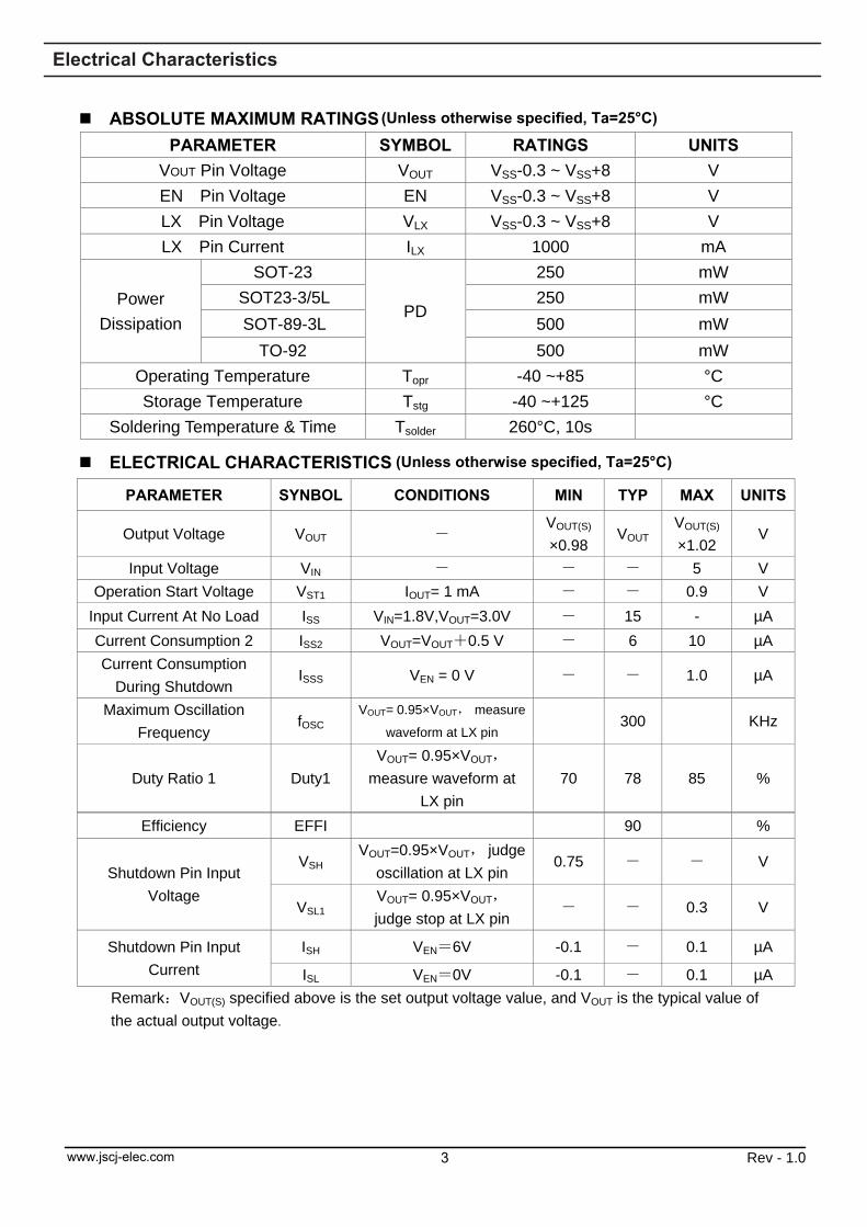
ABSOLUTE MAXIMUM RATINGSPARAMETER SYMBOL RATINGS UNITS
VOUT Pin Voltage VOUT VSS-0.3 ~ VSS+8 V EN Pin Voltage EN VSS-0.3 ~ VSS+8 V LX Pin Voltage VLX VSS-0.3 ~ VSS+8 V LX Pin Current ILX 1000 mA
Power Dissipation
SOT-23
PD
250 mW SOT23-3/5L 250 mW SOT-89-3L 500 mW
TO-92 500 mW Operating Temperature Topr -40 ~+85 °C Storage Temperature Tstg -40 ~+125 °C
Soldering Temperature & Time Tsolder 260°C, 10s
ELECTRICAL CHARACTERISTICS (Unless otherwise specified, Ta=25°C)
PARAMETER SYNBOL CONDITIONS MIN TYP MAX UNITS
Output Voltage VOUT -VOUT(S)
×0.98 VOUT
VOUT(S)
×1.02 V
Input Voltage VIN - - - 5 V Operation Start Voltage VST1 IOUT= 1 mA - - 0.9 V
Input Current At No Load ISS VIN=1.8V,VOUT=3.0V - 15 - µA Current Consumption 2 ISS2 VOUT=VOUT+0.5 V - 6 10 µA Current Consumption
During Shutdown ISSS VEN = 0 V - - 1.0 µA
Maximum Oscillation Frequency
fOSC VOUT= 0.95×VOUT, measure
waveform at LX pin 300 KHz
Duty Ratio 1 Duty1 VOUT= 0.95×VOUT,
measure waveform at LX pin
70 78 85 %
Efficiency EFFI 90 %
Shutdown Pin Input Voltage
VSH VOUT=0.95×VOUT, judge
oscillation at LX pin 0.75 - - V
VSL1 VOUT= 0.95×VOUT, judge stop at LX pin
- - 0.3 V
Shutdown Pin Input Current
ISH VEN=6V -0.1 - 0.1 µA
ISL VEN=0V -0.1 - 0.1 µA Remark:VOUT(S) specified above is the set output voltage value, and VOUT is the typical value of the actual output voltage.
3 Rev - 1.0
(Unless otherwise specified, Ta=25°C)
Electrical Characteristics
www.jscj-elec.com
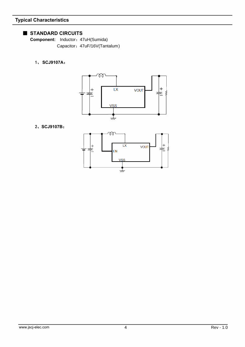
■ STANDARD CIRCUITSComponent: Inductor:47uH(Sumida)
Capacitor:47uF/16V(Tantalum)
1、 SCJ9107A:
2、SCJ9107B:
4 Rev - 1.0
Typical Characteristics
www.jscj-elec.com
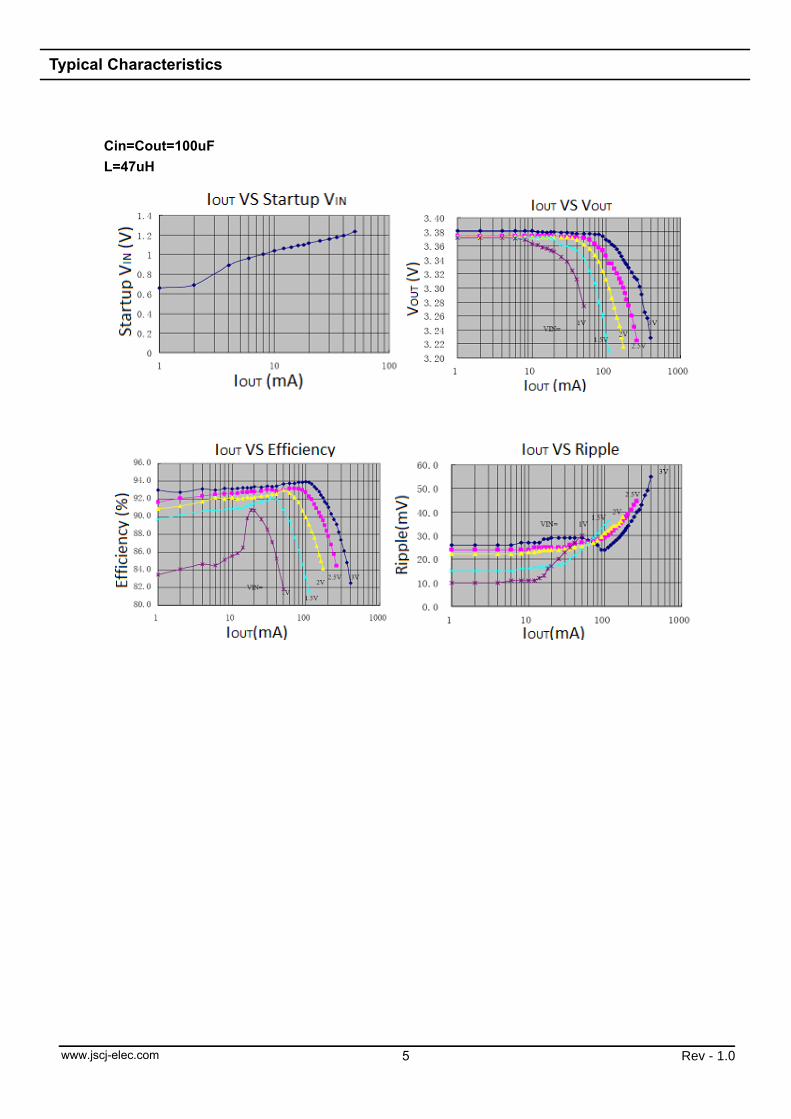
Cin=Cout=100uF L=47uH
5 Rev - 1.0
Typical Characteristics
www.jscj-elec.com

PACKAGE INFORMATION● SOT-23
Synchronous Step-Up DC/DC Converter with PFM Control SCJ9107 Ser ies
6 Rev - 1.0Rev - 1.0Rev - 1.0
Min. Max. Min. Max.A 0.900 1.150 0.035 0.045A1 0.000 0.100 0.000 0.004A2 0.900 1.050 0.035 0.041b 0.300 0.500 0.012 0.020c 0.080 0.150 0.003 0.006D 2.800 3.000 0.110 0.118E 1.200 1.400 0.047 0.055E1 2.250 2.550 0.089 0.100ee1 1.800 2.000 0.071 0.079LL1 0.300 0.500 0.012 0.020θ 0° 8° 0° 8°
0.550 REF. 0.022 REF.
Symbol Dimensions In InchesDimensions In Millimeters
0.950 TYP. 0.037 TYP.
www.jscj-elec.com

8www.jscj-elec.com Rev - 1.0
Symbol Dimensions In Millimeters Dimensions In Inches
Min. Max. Min. Max. A 1.050 1.250 0.041 0.049
A1 0.000 0.100 0.000 0.004 A2 1.050 1.150 0.041 0.045 b 0.300 0.500 0.012 0.020 c 0.100 0.200 0.004 0.008 D 2.820 3.020 0.111 0.119 E 1.500 1.700 0.059 0.067 E1 2.650 2.950 0.104 0.116 e 0.950(BSC) 0.037(BSC) e1 1.800 2.000 0.071 0.079 L 0.300 0.600 0.012 0.024 θ 0° 8° 0° 8°
Package Outline Dimensions ������-3L
������-3L��� ��������������
www.jscj-elec.com

9www.jscj-elec.com Rev - 1.0
Symbol Dimensions In Millimeters Dimensions In Inches
Min. Max. Min. Max. A 1.050 1.250 0.041 0.049
A1 0.000 0.100 0.000 0.004 A2 1.050 1.150 0.041 0.045 b 0.300 0.500 0.012 0.020 c 0.100 0.200 0.004 0.008 D 2.820 3.020 0.111 0.119 E 1.500 1.700 0.059 0.067 E1 2.650 2.950 0.104 0.116 e 0.950(BSC) 0.037(BSC) e1 1.800 2.000 0.071 0.079 L 0.300 0.600 0.012 0.024 θ 0° 8° 0° 8°
Package Outline Dimensions
SOT-23-5L Suggested Pad Layout
SOT-23-5L
www.jscj-elec.com
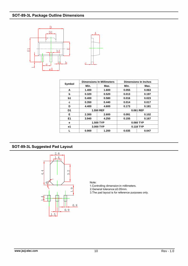
10www.jscj-elec.com Rev - 1.0
Symbol Dimensions In Millimeters Dimensions In Inches
Min. Max. Min. Max. A 1.400 1.600 0.055 0.063 b 0.320 0.520 0.013 0.197
b1 0.400 0.580 0.016 0.023 c 0.350 0.440 0.014 0.017 D 4.400 4.600 0.173 0.181
D1 1.550 REF 0.061 REF E 2.300 2.600 0.091 0.102 E1 3.940 4.250 0.155 0.167 e 1.500 TYP 0.060 TYP e1 3.000 TYP 0.118 TYP L 0.900 1.200 0.035 0.047
SOT-89-3L Package Outline Dimensions
SOT-89-3L Suggested Pad Layout
www.jscj-elec.com

11www.jscj-elec.com Rev - 1.0
Symbol Dimensions In Millimeters Dimensions In Inches
Min. Max. Min. Max. A 3.300 3.700 0.130 0.146
A1 1.100 1.400 0.043 0.055 b 0.380 0.550 0.015 0.022 c 0.360 0.510 0.014 0.020 D 4.400 4.700 0.173 0.185
D1 3.430 0.135 E 4.300 1.400 0.169 0.185 e 1.270 TYP 0.050 TYP e1 2.440 2.640 0.096 0.104 L 14.100 14.500 0.555 0.571 Ф 1.600 0.063 h 0.000 0.380 0.000 0.015
&9:����**������"���5������
&9:��"�-.�*��&�������(� ��������
www.jscj-elec.com
Copyright © JIANGSU CHANGJING ELECTRONICS TECHNOLOGY CO., LTD.
DISCLAIMER
IMPORTANT NOTICE, PLEASE READ CAREFULLYThe information in this data sheet is intended to describe the operation and characteristics of our products. JSCJ has the right to make any modification, enhancement, improvement, correction or other changes to any content in this data sheet, including but not limited to specification parameters, circuit design and application information, without prior notice. Any person who purchases or uses JSCJ products for design shall: 1. Select products suitable for circuit application and design; 2. Design, verify and test the rationality of circuit design; 3. Procedures to ensure that the design complies with relevant laws and regulations and the requirements of such laws and regulations. JSCJ makes no warranty or representation as to the accuracy or completeness of the information contained in this data sheet and assumes no responsibility for the application or use of any of the products described in this data sheet. Without the written consent of JSCJ, this product shall not be used in occasions requiring high quality or high reliability, including but not limited to the following occasions: medical equipment, automotive electronics, military facilities and aerospace. JSCJ shall not be responsible for casualties or property losses caused by abnormal use or application of this product.
Official Website: www.jscj-elec.com