Advanced Char Driver Operations Ted Baker Andy Wang COP 5641 / CIS 4930.

CIS 4930 Digital Circuit TestingDesign For Testability
Dr. Hao ZhengComp Sci & Eng
Univ of South Florida

Introduction• Testing cost– Test gen., fault sim., test equipment, test process (fault
detection and location), etc• Testing should be considering during the design process – enhances “testability” & design quality– reduces test cost
• Test complexity determined by three factors– Controllability– Observability– Predictability – ability to obtain know outputs
• Design for Testability (DFT) techniques are design efforts to ensure that a device is testable
29.1 Testability

Introduction• Testing cost– Test gen., fault sim., test equipment, test process (fault
detection and location), etc• Testing should be considering during the design process • Design for testability (DFT) modifies design to– enhances “testability” & design quality– reduces test cost
• Testability involves– Controllability– Observability– Predictability – ability to obtain know outputs
39.1 Testability
Testability - Controllability• Controllability– ability to establish a specific signal value at each node
in the circuit by setting values on PIs• Circuits difficult to control:– Decoders– Circuits with feedback– Oscillators– Clock generators– Counters (eg., 16 bit counter, how clock cycles will it
take to force MSB to 1?)49.1 Testability

Testability - Observability• Observability– Ability to determine the signal value at any node in a
circuit by controlling circuit’s inputs and observing its outputs
• Circuits difficult to observe:– Sequential circuits– Circuits with global feedback– Embedded RAMs, ROMs, or PLAs– Circuits with redundant nodes
59.1 Testability

Some General Observations• Sequential logic is more difficult to test than
combinational logic• Control logic is more difficult to test than data-
path logic• Random logic is more difficult to test than
structured, bus-oriented designs• Asynchronous designs is more difficult to test
than synchronous designs69.1 Testability

Tradeoffs• DFT techniques often reduce costs to test.– Improved controllability and observability.– Reduced test time, test generation cost, – improved test quality -> product quality
• At meantime, they increase product cost.– Silicon area, I/O pins, power consumption, and circuit
delay.• Need to balance gain from DFT and its cost
79.1 Testability

Ad Hoc DFT Techniques1. Test Points2. Initialization3. Monostable multivibrators (one-shots)4. Oscillators and clocks5. Counters/Shift Registers6. Partitioning Large Circuits7. Logical Redundancy8. Breaking Global Feedback Paths
89.2 Ad Hoc DFT Techniques

1 – Test Points
Two types of test points:• Control points (CP) = PIs used to enhance
controllability• Observation points (OP) = POs used to enhance
observability
9
Employ test points to enhance controllability and observability
9.2 Ad Hoc DFT Techniques

Employing Test Points
10
A is an OPA’ is a CP
0 Injection Ckt
Demand of large # of IO pins!
9.2 Ad Hoc DFT Techniques
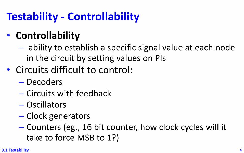
Multiplexing Monitor Points• For limited IO pins, we can use multiplexer• Drawback – can monitor only one OP at a time ->
increases test time• Select lines can be driven by a counter
11
Tradeoff between test time and IO pins.
N clock cycles are required between test vectors
9.2 Ad Hoc DFT Techniques

Demux/Latch for Multiple CPs• Values of 2n control points are serially applied to input Z• Stored in N bit-wide latch• Need N cycles to set up the control values
12
350
R
1
2DE
Z MU
NX
1 2 ... n
Xl X2 Xn
DESIGN FOR TESTABILITY
CPl
CP2
CPN
Figure 9.3 Using a demultiplexer and latch register to implement controlpoints
observation ntest
points
normalfunctional
signals
n
MUX
s
SELECT
(a)
n primaryoutputs
normal nprimaryinputs
DEMUX
S
SELECT
(b)
n
normalfunctional
inputs
R
n controltest
points
Figure 9.4 Time-sharing I/O ports
3. enable and read/write inputs to memory devices;
4. clock and preset/clear inputs to memory devices such as flip-flops, counters, andshift registers;
5. data select inputs to multiplexers and demultiplexers;
6. control lines on tristate devices.
Examples of good candidates for observation points are as follows:
9.2 Ad Hoc DFT Techniques

Time-Sharing Normal I/O Pins
139.2 Ad Hoc DFT Techniques

Signal Selection – Control Points • Control, address, and data bus lines on bus-
structured designs• Enable/hold inputs to microprocessors• Enable and read/write inputs to memory devices• Clock and preset/clear inputs to memory devices• Data select inputs to muxes/demuxes• Control lines on tri-state devices
149.2 Ad Hoc DFT Techniques

Signal Selection – Observation Points• Stem lines associated with signals having high
fanout• Global feedback paths• Redundant signal lines• Outputs of logic devices having many inputs
(muxes, parity generators)• Outputs from state devices (FFs, Counters, Shift
Registers)• Address, control, and data busses
159.2 Ad Hoc DFT Techniques

2 – Initialization
16
Design circuits to be easily initializable
Should be avoided!
9.2 Ad Hoc DFT Techniques

17
Set/reset controlled by logic gates
Set/reset signal controlled internally
9.2 Ad Hoc DFT Techniques

5 – Partitioning Counters and Shift Registers
• Counters/SR are difficult to test because test sequences usually require many clock cycles
• Partition the register for better control/obs.
18
Partition large counters and shift registers into smaller units
9.2 Ad Hoc DFT Techniques

199.2 Ad Hoc DFT Techniques

6. Partitioning of Large Comb. Circuits
• Time complexity of test generation grows faster than a linear function of circuit size
• Partitioning can reduce the test generation cost
20
Ad Hoc Design for Testability Techniques
B
sA C
m n\11 \1 \11 \1
D,:::..
p
C 1 C 2
..:::,Eq
t t
357
B
F(a)
G
A
D
A'
C
F
o 1MUX S
C 2 T 1 T 2 ModeS 1 C' 0 0 normalM 0 1 test C 1UX 0 E 1 0 test C 2
G
1 0S MUX
F'(b)
G'
Figure 9.11 Partitioning to reduce test generation cost
Partition large circuits into small subcircuits to reduce test generation costs.
9.2 Ad Hoc DFT Techniques

Ad Hoc Design for Testability Techniques
B
sA C
m n\11 \1 \11 \1
D,:::..
p
C 1 C 2
..:::,Eq
t t
357
B
F(a)
G
A
D
A'
C
F
o 1MUX S
C 2 T 1 T 2 ModeS 1 C' 0 0 normalM 0 1 test C 1UX 0 E 1 0 test C 2
G
1 0S MUX
F'(b)
G'
Figure 9.11 Partitioning to reduce test generation cost21
Ad Hoc Design for Testability Techniques
B
sA C
m n\11 \1 \11 \1
D,:::..
p
C 1 C 2
..:::,Eq
t t
357
B
F(a)
G
A
D
A'
C
F
o 1MUX S
C 2 T 1 T 2 ModeS 1 C' 0 0 normalM 0 1 test C 1UX 0 E 1 0 test C 2
G
1 0S MUX
F'(b)
G'
Figure 9.11 Partitioning to reduce test generation cost
9.2 Ad Hoc DFT Techniques

7 – Logical Redundancy• Rule: Avoid the use of redundant logic.• Redundancy makes faults undetectable• It may invalidate some test for nonredundant faults• Can cause difficulty in fault coverage calculations• Redundancy can be introduced inadvertantly– Maybe difficult to remove.– Test points can be added to remove redundancy during testing
229.2 Ad Hoc DFT Techniques

Scan Registers• Test points are costly in terms of I/O pins• Scan Register is an alternative – tradeoff between
test time, area, and I/O pins• Scan Register (SR) = Register with both shift and
parallel-load capability• Storage cells in SR can be used as observation and
control points
239.3 Scan Registers

Scan Storage Cell (SSC)
24
Controllability and Observability by Means of Scan Registers 359
sseD Q, SO
s, D
sseNIT
CK
(a) (b)
D 1 Ql D 2 Q2 Dn Qn
Sin SOU!
NIT
CK
(c)
(d)
Figure 9.12 (a) A scan storage cell (SSC) (b) Symbol for a sse (c) A scanregister (SR) or shift register chain (d) Symbol for a scan register
Simultaneous Controllability and Observability
Figure 9.13(a) shows two complex circuits C 1 and C 2 • They can be eithercombinational or sequential. Only one signal (Z) between C 1 and C 2 is shown.
Figure 9.13(b) depicts how line Z can be made both observable and controllable usinga scan storage cell. Data at Z can be loaded into the sse and observed by means of ascan-out operation. Data can be loaded into the sse via a scan-in operation and theninjected onto line Z'. Simultaneous controllability and observability can be achieved.That is, the scan register can be preloaded with data to be injected into the circuit.
N/T = 0
N/T = 1
Normal mode: D is loaded
Testing mode: S is loaded
9.3 Scan Registers

Scan Register
25
Controllability and Observability by Means of Scan Registers 359
sseD Q, SO
s, D
sseNIT
CK
(a) (b)
D 1 Ql D 2 Q2 Dn Qn
Sin SOU!
NIT
CK
(c)
(d)
Figure 9.12 (a) A scan storage cell (SSC) (b) Symbol for a sse (c) A scanregister (SR) or shift register chain (d) Symbol for a scan register
Simultaneous Controllability and Observability
Figure 9.13(a) shows two complex circuits C 1 and C 2 • They can be eithercombinational or sequential. Only one signal (Z) between C 1 and C 2 is shown.
Figure 9.13(b) depicts how line Z can be made both observable and controllable usinga scan storage cell. Data at Z can be loaded into the sse and observed by means of ascan-out operation. Data can be loaded into the sse via a scan-in operation and theninjected onto line Z'. Simultaneous controllability and observability can be achieved.That is, the scan register can be preloaded with data to be injected into the circuit.
Normal mode (N/T = 0) load data (Dx) in parallelTest mode (N/T = 1) shift data (from Sin to Sout)

Simultaneous Controllability and Observability
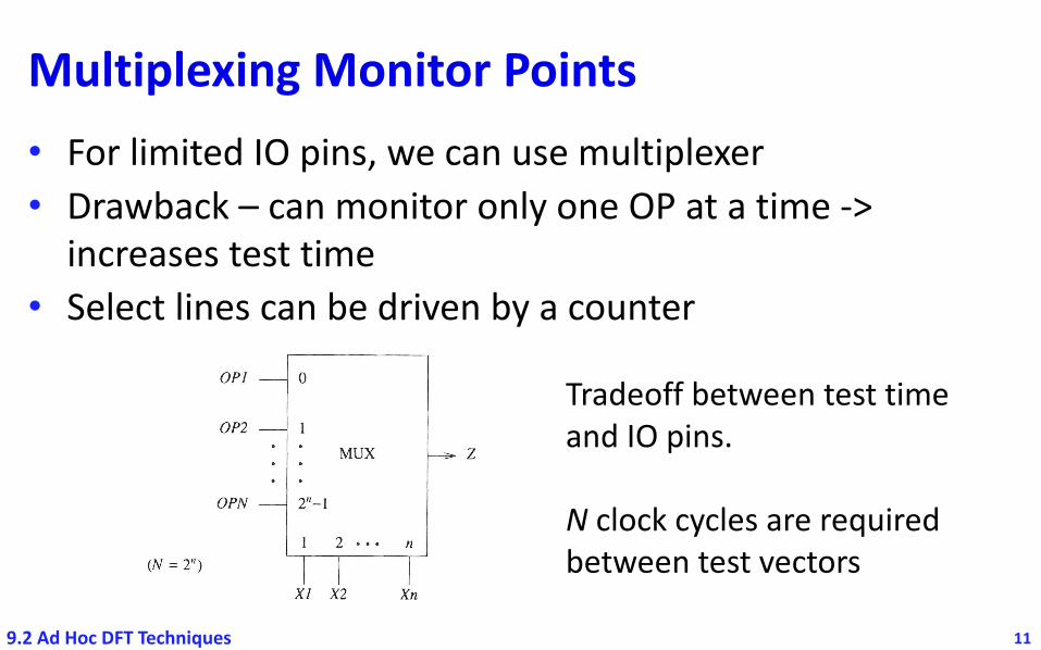
26
• C1 and C2 can be sequential/combinational• Z can be loaded into SSC via scan-in and observed by
scan-out operation• Data can be loaded in SSC via D-input and injected onto
line Z’
Separate Controllability and Observability
27
Z’ is connected to D-input.CP is connected to Scan-in.
9.3 Scan Registers

Observability Only
289.3 Scan Registers

Controllability Only
299.3 Scan Registers

Making Undetectable Faults Detectable
30
• X’ = Control points Z’ = Observation points• Lets say f is an undetectable fault• Choose X’ and Z’ such that f becomes detectable• R1 and R2 can be combined as a single register
9.3 Scan Registers

Example 1 – Enhancing Testability
31
• C1, C2, … C6 are Complex Seq/Comb blocks.• # of CPs and OPs decides the length of scan register.• How does it work?

Generic Scan-Based Designs• Scan Design – most popular structured DFT
technique, employs a scan register• Several forms of scan designs – differ primarily in
the scan cell design• Three generic forms of scan design– Full Serial Integrated Scan– Isolated Serial Scan– Non-serial Scan
32

Full Serial Integrated Scan
33
Instead of testing circuit in (a) as a sequential circuit, now C can be tested using a series of test vectors.
All storage elements in the design become part of scan register.

Isolated Serial Scan
34
• Unlike Full Serial, Scan register is not part of the data path
Shadow register : does not interfere the normal operation, but add substantial area overhead.
Rs

Non-Serial Scan
35
RAM is used instead of shift register.
Individual bits can be modified for selected CPs or OPs.
Area overhead is high.

Generic Boundary Scan• Concept – in designing modules such as complex
chips or PCBs, for local testing and fault isolation, we should be able to isolate one module from another
• All chips on board are designed using boundary scan architecture
• Boundary scan registers are on the periphery; not part of the function
• Test vectors can be scanned in and responses saved and scanned out
• Internal clock must be disabled36

Generic Boundary Scan
37

Boundary-Scan Standards• Goal – to ensure chips of VLSI complexity contain standard DFT
circuitry to make test development effective and less costly• Some initiatives
– Joint Test Action Group (JTAG) Boundary Scan Std– VHSIC Element Test and Maintenance (IBM Std)– IEEE 1149.1 Testability Bus Standard
• Primarily deal with– Test Bus (resides on the board)– Bus Protocol– Interface logic between test bus ports and DFT hardware
• JTAG Boundary Scan and IEEE 1149.1 require a bound-scan register exist on the chip
38

39
TAP = Test Access Port• TDI = Test Data Input• TDO = Test Data Output• TMS = Test Mode Signal• TCK = Test Clock
TAP Controller = a FSM control operation of test bus
Boundary-Scan Standards 397
OPTIONAL
Sout ::::::::::::::::::::::::::::::::
APPLICATION LOGIC
Sin::::::::::::::::::::::::::::::::::
.: : : : : : : .: BIST registers :::::::::::: : : : : : : :: Scan registers ::::::::::
Boundary-scan pathIIII
Instructionregister
Miscellaneousregisters
Bypassregister
BS test bus circuitry
...............................................................................
Boundary-scan cell/
I/O Pad //
/
/
.
Figure 9.45 Chip architecture for IEEE 1149.1
9.10.2 Boundary-Scan Cell
Two possible boundary-scan cell designs are shown in Figure 9.46. These cells can beused as either output or input cells. Other cell designs exist for bidirectional I/O ports andtristate outputs.
As an input boundary-scan cell, IN corresponds to a chip input pad, and OUT is tied to anormal input to the application logic. As an output cell, IN corresponds to the output ofthe application logic, and OUT is tied to an output pad. The cell has several modes ofoperations.
Normal Mode: When Mode_Control=O, data passes from port IN to port OUT; then thecell is transparent to the application logic.

Test Bus Operation1. Instruction sent serially over the TDI line into the
instruction register2. Selected test circuitry is configured to respond to
the instruction– More data needed to configure data registers
3. The test instruction is executed. Test results can be shifted out of selected registers and transmitted over TDO line to the bus master. Data can shifted in while results are shifted out.
40

Boundary Scan Cell
41
• Normal Mode: Mode_Control = 0, cell is transparent• Scan Mode – Boundary cells are interconnected into a scan path (TDI input, TDO output) ShiftDR =1 and Clock pulses applied to ClockDR• Capture Mode – ShiftDR = 0 => input IN is captured• Update Mode – Once QA is loaded (by scan/capture), set Mode_control = 1 and apply a clock pulse to UpdateDR for the value in QA applied to OUT
Application logic

Boundary Scan Cell – Another Design
42

PCB with IEEE 1149.1 test bus
43
• Interconnect Test• System Snapshot• Chip Test
400 DESIGN FOR TESTABILITY
- TDI
TDO
Figure 9.47 A printed circuit board with a IEEE 1149.1 test bus
9.10.4 The Test BusA board supporting IEEE 1149.1 contains a test bus consisting of at least four signals. (Afifth signal can be used to reset the on-chip test-bus circuitry.) These signals areconnected to a chip via its test-bus ports. Each chip is considered to be a bus slave, andthe bus is assumed to be driven by a bus master.
The minimum bus configuration consists of two broadcast signals (TMS and TCK) drivenby the master, and a serial path formed by a "daisy-chain" connection of serial scan datapins (TDI and TDO) on the master and slave devices. Figure 9.51(a) shows a ringconfiguration; Figure 9.51(b) shows a star configuration, where each chip is associatedwith its own TMS signal. Star and ring configurations can be combined into hybridconfigurations. The four bus signals associated with a slave TAP are defined as follows.
TCK - Test Clock. This is the master clock used during the boundary-scan process.
TDI - Test Data Input. Data or instructions are received via this line and are directed toan appropriate register within the application chip or test bus circuitry.

PCB Test – Three modes• External Test Mode– Test interconnects between chips
• Sample Test Mode– I/O data of a chip can be sampled during normal system
operation – snapshots of chip IO data– Sampled data can be scanned out while board is in normal
operation• Internal Test Mode– Inputs to the application logic is driven by the input
boundary-scan cells and response captured in output boundary-scan cells
44

Boundary-Scan Standards 401
Chip 1 Chip 2
Output SOUT
Mode Input SOUT
Control Mode
ControlMUX
MUX0
Application0 Application
logiclogic
MUX
MUX0
Q D Q D 0
Q B Q A Q D Q D
Q B Q A
ShiftDRUpdateDR ClockDR SIN
UpdateDR ClockDR SIN ShiftDR
Figure 9.48 External test configuration
TDO - Test Data Output. The contents of a selected register (instruction or data) areshifted out of the chip over TDO.
TMS - Test Mode Selector. The value on TMS is used to control a finite state machinein a slave device so that this device knows when to accept test data or instructions.
Though the IEEE 1149.1 bus employs only a single clock, TCK, this clock can bedecoded on-chip to generate other clocks, such as the two-phase nonoverlap clocks usedin implementing LSSD.
9.10.5 Test-Bus Circuitry
The on-chip test-bus circuitry allows access to and control of the test features of a chip.A simplified version of this circuitry is shown in Figure 9.45, and more details are shownin Figure 9.52. This circuitry consists of four main elements, namely (1) a test accessport (TAP) consisting of the ports associated with TMS, TCK, TDI, and TDI, (2) a TAPcontroller, (3) a scannable instruction register and associated logic, and (4) a group ofscannable test data registers. We will next elaborate on some of these features.
9.10.5.1 The TAP Controller
The TAP controller is a synchronous finite-state machine whose state diagram is shownin Figure 9.53. It has a single input, labeled TMS, and its outputs are signalscorresponding to a subset of the labels associated with the various states, such asCapture-IR. The state diagram shows that there are two parallel and almost identical
External Test Configuration
45
UpdateOperation Capture
Operation
402
Input
Mode
Control
MUX
SOUT
MUX
o
DESIGN FOR TESTABILITY
Output SOUT
Mode
Control
MUXApplication
logic 0
MUX
UpdateDR ClockDR SIN ShiftDR
UpdateDR ClockDR
o
SIN ShiftDR
Figure 9.49 Sample test configuration
subdiagrams, one corresponding to controlling the operations of the instruction register,the other to controlling the operation of a data register. The controller can change stateonly when a clock pulse on TCK occurs; the next state is determined by the logic level ofline TMS. The function of some of these control states is described below.
Test-Logic-Reset: In this state the test logic (boundary-scan) is disabled so that theapplication logic can operate in its normal mode.
Run-Test/Idle: This is a control state that exists between scan operations, and where aninternal test, such as a built-in self-test, can be executed (see instruction RUNBIST).
A test is selected by first setting the instruction register with the appropriate information.The TAP controller remains in this state as long as TMS=O.
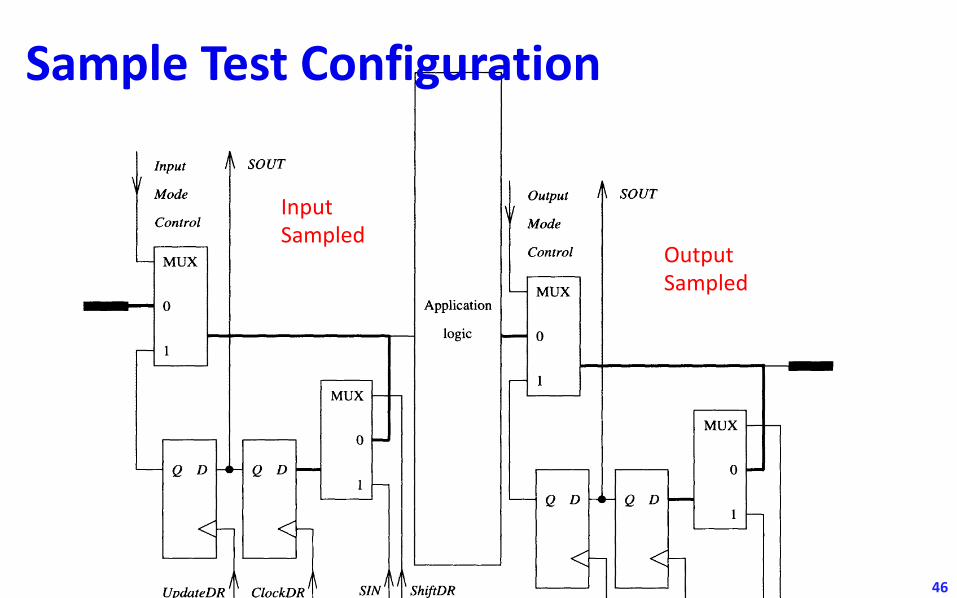
Seleet-DR-Sean: This is a temporary controller state. If TMS is held low then a scan-datasequence for the selected test-data register is initiated, starting with a transition to thestate Capture-DR.
Capture-DR: In this state data can be loaded in parallel into the test-data registersselected by the current instruction. For example, the boundary-scan registers can beloaded while in this state. Referring to Figure 9.49, to capture the data on the input padshown and the output of the application logic, it is necessary to set ShiftDR low and toactivate the clock line CloekDR.
Sample Test Configuration
46
InputSampled
OutputSampled

Internal Test Configuration
47
Inputs from I/P BS cells Response
Collected intoO/P BS cells

48
404
Application chips
TDITCK
#1TMS
Bus TDOmaster
TDO TDITCK
TDI #2TMS
TMS TDO
•TCK ••TDITCK
#NTMSTDO
(a)
DESIGN FOR TESTABILITY
Application chips
:- TDITCK
#1TMS
Bus TDOmaster
TDO -.. TDI-TDITMSl TCK
#2TMS2 :.. TMS
• •• • TDO• •TMSN - 1---- •
TCK ••::- TDI
TCK#N
-.. TMS-TDO
(b)
Figure 9.51 (a) Ring configuration (b) Star configuration
The states that control the instruction register operate similarly to those controlling thetest-data registers. The instruction register is implemented using a latched parallel-outputfeature. This way a new instruction can be scanned into the scan path of the instructionregister without affecting the output of the register. The Select-IR-Scan state is again atemporary transition state. In the Capture-IR state, the shift register associated with theinstruction register is loaded in parallel. These data can be status information and/orfixed logic values. In the Shift-IR state this shift register is connected between TDI andTDO and shifts data one position. In the Update-IR control state the instruction shiftedinto the instruction register is latched onto the parallel output of the instruction register.This instruction now becomes the current instruction.
The TAP controller can be implemented using four flip-flops and about two dozen logicgates.
9.10.5.2 Registers
The Instruction Register and Commands
The instruction register has the ability to shift in a new instruction while holding thecurrent instruction fixed at its output ports. The register can be used to specify operationsto be executed and select test-data registers. Each instruction enables a single serial test-data register path between TDI and TDO. The instructions BYPASS, EXTEST, and

49
IEEE 1149.1 Test Bus Circuitry• TAP – TCK, TMS, TDI, TDO• Test DR• Scannable IR• TAP controller

50
State Diagram of
TAP Controller
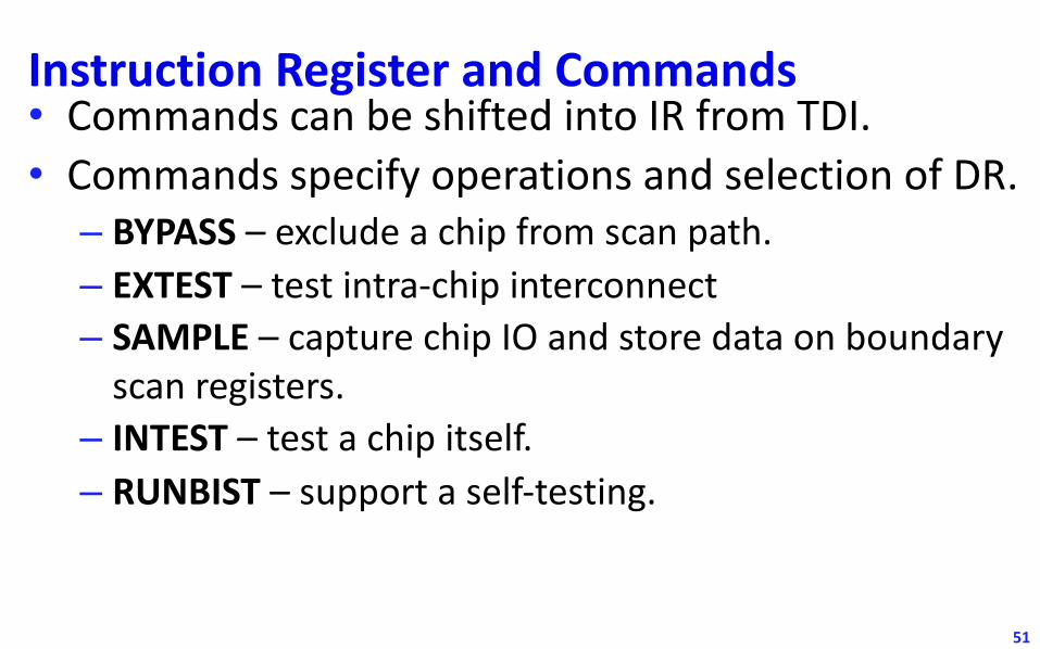
Instruction Register and Commands• Commands can be shifted into IR from TDI.• Commands specify operations and selection of DR.– BYPASS – exclude a chip from scan path.– EXTEST – test intra-chip interconnect– SAMPLE – capture chip IO and store data on boundary
scan registers.– INTEST – test a chip itself.– RUNBIST – support a self-testing.
51

52
Backup

3 – Monostable Multivibrators
53
Rule: Disable internal one-shots during test• One-shots provide pulses internal to circuit• Difficult for ATE to remain in synchronization with the circuit354
1
JlII
one-shot
(a)
1/0-1
DESIGN FOR TESTABILITY
jumperI
2 V
A
B
C
D
IIIIIIL _
(b)
n E (OP)
Figure 9.8 (a) Disabling a one-shot using jumpers (b) Logical control anddisabling of a one-shot
9.2.5 Partitioning Counters and Shift Registers
Rule: Partition large counters and shift registers into smaller units.
Counters, and to a lesser extent shift registers, are difficult to test because their testsequences usually require many clock cycles. To increase their testability, suchdevices should be partitioned so that their serial input and clock are easily controllable,and output data are observable. Figure 9.10(a) shows a design that does not includetestability features and where the register R has been decomposed into two parts, andFigure 9.10(b) shows a more testable version of this design. For example, Rl and R2may be 16-bit registers. Here the gated clock from C can be inhibited and replaced byan external clock. The serial inputs to Rl and R2 are easily controlled and the serialoutput of R2 is easily observable. As a result, Rl and R2 can be independently tested.

354
1
JlII
one-shot
(a)
1/0-1
DESIGN FOR TESTABILITY
jumperI
2 V
A
B
C
D
IIIIIIL _
(b)
n E (OP)
Figure 9.8 (a) Disabling a one-shot using jumpers (b) Logical control anddisabling of a one-shot
9.2.5 Partitioning Counters and Shift Registers
Rule: Partition large counters and shift registers into smaller units.
Counters, and to a lesser extent shift registers, are difficult to test because their testsequences usually require many clock cycles. To increase their testability, suchdevices should be partitioned so that their serial input and clock are easily controllable,and output data are observable. Figure 9.10(a) shows a design that does not includetestability features and where the register R has been decomposed into two parts, andFigure 9.10(b) shows a more testable version of this design. For example, Rl and R2may be 16-bit registers. Here the gated clock from C can be inhibited and replaced byan external clock. The serial inputs to Rl and R2 are easily controlled and the serialoutput of R2 is easily observable. As a result, Rl and R2 can be independently tested.
3 – Monostable Multivibrators
54
Rule: Disable internal one-shots during test• One-shots provide pulses internal to circuit• Difficult for ATE to remain in synchronization with the circuit

4 – Oscillators and Clocks
55
Rule: Disable internal oscillators/clocks during test