
CircuiTikZ 1.0 - manual - Dalhousie...
164
20 21 19 22 18 23 17 24 16 25 15 26 14 27 13 28 12 29 11 30 10 31 9 32 8 33 7 34 6 35 5 36 4 37 3 38 2 39 1 40 CircuiTik Z Massimo A. Redaelli [email protected] Stefan Lindner [email protected] Stefan Erhardt [email protected] Romano Giannetti [email protected] CircuiTikZ version 1.0.2 (2020/03/22) Massimo A. Redaelli ([email protected]) Stefan Lindner ([email protected]) Stefan Erhardt ([email protected]) Romano Giannetti ([email protected]) March 22, 2020
Transcript of CircuiTikZ 1.0 - manual - Dalhousie...

20
21
19
22
18
23
17
24
16
25
15
26
14
27
13
28
12
29
11
30
10
31
9
32
8
33
7
34
6
35
5
36
4
37
3
38
2
39
1
40
CircuiTikZ
Massimo A. [email protected]
Stefan [email protected]
Stefan [email protected]
Romano [email protected]
CircuiTikZversion 1.0.2 (2020/03/22)
Massimo A. Redaelli ([email protected])Stefan Lindner ([email protected])Stefan Erhardt ([email protected])
Romano Giannetti ([email protected])
March 22, 2020

Contents
1 Introduction 61.1 About . . . . . . . . . . . . . . . . . . . . . . . . . . . . . . . . . . . . . . . . . . . 61.2 License . . . . . . . . . . . . . . . . . . . . . . . . . . . . . . . . . . . . . . . . . . . 61.3 Loading the package . . . . . . . . . . . . . . . . . . . . . . . . . . . . . . . . . . . 61.4 Installing a new version of the package. . . . . . . . . . . . . . . . . . . . . . . . . 71.5 Requirements . . . . . . . . . . . . . . . . . . . . . . . . . . . . . . . . . . . . . . . 71.6 Incompatible packages . . . . . . . . . . . . . . . . . . . . . . . . . . . . . . . . . . 71.7 Known bugs and limitation . . . . . . . . . . . . . . . . . . . . . . . . . . . . . . . 71.8 Scale factors inaccuracies . . . . . . . . . . . . . . . . . . . . . . . . . . . . . . . . 81.9 Incompabilities between version . . . . . . . . . . . . . . . . . . . . . . . . . . . . . 81.10 Feedback . . . . . . . . . . . . . . . . . . . . . . . . . . . . . . . . . . . . . . . . . 91.11 Package options . . . . . . . . . . . . . . . . . . . . . . . . . . . . . . . . . . . . . . 9
2 Tutorials 132.1 Getting started with CircuiTikZ: a current shunt . . . . . . . . . . . . . . . . . . . 132.2 A more complex tutorial: circuits, Romano style. . . . . . . . . . . . . . . . . . . . 15
3 The components 213.1 Path-style components . . . . . . . . . . . . . . . . . . . . . . . . . . . . . . . . . . 21
3.1.1 Anchors . . . . . . . . . . . . . . . . . . . . . . . . . . . . . . . . . . . . . . 213.1.2 Customization . . . . . . . . . . . . . . . . . . . . . . . . . . . . . . . . . . 22
3.1.2.1 Components size . . . . . . . . . . . . . . . . . . . . . . . . . . . . 223.1.2.2 Thickness of the lines . . . . . . . . . . . . . . . . . . . . . . . . . 233.1.2.3 Shape of the components . . . . . . . . . . . . . . . . . . . . . . . 24
3.1.3 Descriptions . . . . . . . . . . . . . . . . . . . . . . . . . . . . . . . . . . . . 243.2 Node-style components . . . . . . . . . . . . . . . . . . . . . . . . . . . . . . . . . . 25
3.2.1 Mirroring and flipping . . . . . . . . . . . . . . . . . . . . . . . . . . . . . . 253.2.2 Anchors . . . . . . . . . . . . . . . . . . . . . . . . . . . . . . . . . . . . . . 263.2.3 Descriptions . . . . . . . . . . . . . . . . . . . . . . . . . . . . . . . . . . . . 26
3.3 Styling circuits and components . . . . . . . . . . . . . . . . . . . . . . . . . . . . . 273.3.1 Relative size . . . . . . . . . . . . . . . . . . . . . . . . . . . . . . . . . . . 273.3.2 Fill color . . . . . . . . . . . . . . . . . . . . . . . . . . . . . . . . . . . . . 293.3.3 Line thickness . . . . . . . . . . . . . . . . . . . . . . . . . . . . . . . . . . . 303.3.4 Style files . . . . . . . . . . . . . . . . . . . . . . . . . . . . . . . . . . . . . 303.3.5 Style files: how to write them . . . . . . . . . . . . . . . . . . . . . . . . . . 31
3.4 Grounds and supply voltages . . . . . . . . . . . . . . . . . . . . . . . . . . . . . . 323.4.1 Grounds . . . . . . . . . . . . . . . . . . . . . . . . . . . . . . . . . . . . . . 32
3.4.1.1 Grounds anchors . . . . . . . . . . . . . . . . . . . . . . . . . . . . 333.4.1.2 Grounds customization . . . . . . . . . . . . . . . . . . . . . . . . 33
1

3.4.2 Power supplies . . . . . . . . . . . . . . . . . . . . . . . . . . . . . . . . . . 333.4.2.1 Power supply anchors . . . . . . . . . . . . . . . . . . . . . . . . . 333.4.2.2 Power supplies customization . . . . . . . . . . . . . . . . . . . . . 33
3.5 Resistive bipoles . . . . . . . . . . . . . . . . . . . . . . . . . . . . . . . . . . . . . 343.5.1 Potentiometers: wiper position . . . . . . . . . . . . . . . . . . . . . . . . . 363.5.2 Generic sensors anchors . . . . . . . . . . . . . . . . . . . . . . . . . . . . . 363.5.3 Resistive components customization . . . . . . . . . . . . . . . . . . . . . . 37
3.6 Capacitors and inductors: dynamical bipoles . . . . . . . . . . . . . . . . . . . . . 373.6.1 Capacitors . . . . . . . . . . . . . . . . . . . . . . . . . . . . . . . . . . . . 373.6.2 Capacitive sensors anchors . . . . . . . . . . . . . . . . . . . . . . . . . . . . 383.6.3 Capacitors customizations . . . . . . . . . . . . . . . . . . . . . . . . . . . . 383.6.4 Inductors . . . . . . . . . . . . . . . . . . . . . . . . . . . . . . . . . . . . . 383.6.5 Inductors customizations . . . . . . . . . . . . . . . . . . . . . . . . . . . . 393.6.6 Inductors anchors . . . . . . . . . . . . . . . . . . . . . . . . . . . . . . . . 40
3.7 Diodes and such . . . . . . . . . . . . . . . . . . . . . . . . . . . . . . . . . . . . . 403.7.1 Tripole-like diodes . . . . . . . . . . . . . . . . . . . . . . . . . . . . . . . . 423.7.2 Triacs anchors . . . . . . . . . . . . . . . . . . . . . . . . . . . . . . . . . . 433.7.3 Diode customizations . . . . . . . . . . . . . . . . . . . . . . . . . . . . . . 43
3.8 Sources and generators . . . . . . . . . . . . . . . . . . . . . . . . . . . . . . . . . . 443.8.1 Batteries . . . . . . . . . . . . . . . . . . . . . . . . . . . . . . . . . . . . . 443.8.2 Stationary sources . . . . . . . . . . . . . . . . . . . . . . . . . . . . . . . . 443.8.3 Sinusoidal sources . . . . . . . . . . . . . . . . . . . . . . . . . . . . . . . . 453.8.4 Controlled sources . . . . . . . . . . . . . . . . . . . . . . . . . . . . . . . . 463.8.5 Noise sources . . . . . . . . . . . . . . . . . . . . . . . . . . . . . . . . . . . 473.8.6 Special sources . . . . . . . . . . . . . . . . . . . . . . . . . . . . . . . . . . 483.8.7 DC sources . . . . . . . . . . . . . . . . . . . . . . . . . . . . . . . . . . . . 483.8.8 Sources customizations . . . . . . . . . . . . . . . . . . . . . . . . . . . . . . 49
3.9 Instruments . . . . . . . . . . . . . . . . . . . . . . . . . . . . . . . . . . . . . . . . 493.9.1 Instruments customizations . . . . . . . . . . . . . . . . . . . . . . . . . . . 503.9.2 Rotation-invariant elements . . . . . . . . . . . . . . . . . . . . . . . . . . . 503.9.3 Instruments as node elements . . . . . . . . . . . . . . . . . . . . . . . . . . 513.9.4 Measuring voltage and currents, multiple ways . . . . . . . . . . . . . . . . 51
3.10 Mechanical Analogy . . . . . . . . . . . . . . . . . . . . . . . . . . . . . . . . . . . 543.10.1 Mechanical elements customizations . . . . . . . . . . . . . . . . . . . . . . 54
3.11 Miscellaneous bipoles . . . . . . . . . . . . . . . . . . . . . . . . . . . . . . . . . . . 553.11.1 Miscellanous element customization . . . . . . . . . . . . . . . . . . . . . . 56
3.12 Multiple wires (buses) . . . . . . . . . . . . . . . . . . . . . . . . . . . . . . . . . . 563.13 Crossings . . . . . . . . . . . . . . . . . . . . . . . . . . . . . . . . . . . . . . . . . 573.14 Arrows . . . . . . . . . . . . . . . . . . . . . . . . . . . . . . . . . . . . . . . . . . . 58
3.14.1 Arrows size . . . . . . . . . . . . . . . . . . . . . . . . . . . . . . . . . . . . 583.15 Terminal shapes . . . . . . . . . . . . . . . . . . . . . . . . . . . . . . . . . . . . . 59
2

3.15.1 BNC connector/terminal . . . . . . . . . . . . . . . . . . . . . . . . . . . . 603.16 Block diagram components . . . . . . . . . . . . . . . . . . . . . . . . . . . . . . . 60
3.16.1 Blocks anchors . . . . . . . . . . . . . . . . . . . . . . . . . . . . . . . . . . 623.16.2 Blocks customization . . . . . . . . . . . . . . . . . . . . . . . . . . . . . . . 63
3.16.2.1 Multi ports . . . . . . . . . . . . . . . . . . . . . . . . . . . . . . . 643.16.2.2 Labels and custom two-port boxes . . . . . . . . . . . . . . . . . . 643.16.2.3 Box option . . . . . . . . . . . . . . . . . . . . . . . . . . . . . . . 643.16.2.4 Dash optional parts . . . . . . . . . . . . . . . . . . . . . . . . . . 64
3.17 Transistors . . . . . . . . . . . . . . . . . . . . . . . . . . . . . . . . . . . . . . . . 643.17.1 Standard bipolar transistors . . . . . . . . . . . . . . . . . . . . . . . . . . . 643.17.2 Multi-terminal bipolar transistors . . . . . . . . . . . . . . . . . . . . . . . . 663.17.3 Field-effect transistors . . . . . . . . . . . . . . . . . . . . . . . . . . . . . . 663.17.4 Transistor texts (labels) . . . . . . . . . . . . . . . . . . . . . . . . . . . . . 683.17.5 Transistors customization . . . . . . . . . . . . . . . . . . . . . . . . . . . . 68
3.17.5.1 Size. . . . . . . . . . . . . . . . . . . . . . . . . . . . . . . . . . . . 683.17.5.2 Arrows. . . . . . . . . . . . . . . . . . . . . . . . . . . . . . . . . . 683.17.5.3 Body diodes and similar things. . . . . . . . . . . . . . . . . . . . 693.17.5.4 Schottky transistors. . . . . . . . . . . . . . . . . . . . . . . . . . . 703.17.5.5 Base/Gate terminal. . . . . . . . . . . . . . . . . . . . . . . . . . . 703.17.5.6 Bulk terminals. . . . . . . . . . . . . . . . . . . . . . . . . . . . . . 71
3.17.6 Multiple terminal transistors customization . . . . . . . . . . . . . . . . . . 713.17.7 Transistors anchors . . . . . . . . . . . . . . . . . . . . . . . . . . . . . . . . 723.17.8 Transistor paths . . . . . . . . . . . . . . . . . . . . . . . . . . . . . . . . . 74
3.18 Electronic Tubes . . . . . . . . . . . . . . . . . . . . . . . . . . . . . . . . . . . . . 753.18.1 Tubes customization . . . . . . . . . . . . . . . . . . . . . . . . . . . . . . . 77
3.19 RF components . . . . . . . . . . . . . . . . . . . . . . . . . . . . . . . . . . . . . . 793.19.1 RF elements customization . . . . . . . . . . . . . . . . . . . . . . . . . . . 803.19.2 Microstrip customization . . . . . . . . . . . . . . . . . . . . . . . . . . . . 81
3.20 Electro-Mechanical Devices . . . . . . . . . . . . . . . . . . . . . . . . . . . . . . . 813.20.1 Electro-Mechanical Devices anchors . . . . . . . . . . . . . . . . . . . . . . 81
3.21 Double bipoles (transformers) . . . . . . . . . . . . . . . . . . . . . . . . . . . . . . 823.21.1 Double dipoles anchors . . . . . . . . . . . . . . . . . . . . . . . . . . . . . . 833.21.2 Double dipoles customization . . . . . . . . . . . . . . . . . . . . . . . . . . 843.21.3 Styling transformer’s coils independently . . . . . . . . . . . . . . . . . . . . 86
3.22 Amplifiers . . . . . . . . . . . . . . . . . . . . . . . . . . . . . . . . . . . . . . . . . 873.22.1 Amplifiers anchors . . . . . . . . . . . . . . . . . . . . . . . . . . . . . . . . 883.22.2 Amplifiers customization . . . . . . . . . . . . . . . . . . . . . . . . . . . . . 90
3.22.2.1 European-style amplifier customization . . . . . . . . . . . . . . . 913.22.3 Designing your own amplifier . . . . . . . . . . . . . . . . . . . . . . . . . . 93
3.23 Switches and buttons . . . . . . . . . . . . . . . . . . . . . . . . . . . . . . . . . . . 933.23.1 Traditional switches . . . . . . . . . . . . . . . . . . . . . . . . . . . . . . . 93
3

3.23.2 Cute switches . . . . . . . . . . . . . . . . . . . . . . . . . . . . . . . . . . . 943.23.2.1 Cute switches anchors . . . . . . . . . . . . . . . . . . . . . . . . . 953.23.2.2 Cute switches customization . . . . . . . . . . . . . . . . . . . . . 96
3.23.3 Rotary switches . . . . . . . . . . . . . . . . . . . . . . . . . . . . . . . . . . 963.23.3.1 Rotary switch anchors . . . . . . . . . . . . . . . . . . . . . . . . . 973.23.3.2 Rotary switch customization . . . . . . . . . . . . . . . . . . . . . 98
3.24 Logic gates . . . . . . . . . . . . . . . . . . . . . . . . . . . . . . . . . . . . . . . . 993.24.1 American Logic gates . . . . . . . . . . . . . . . . . . . . . . . . . . . . . . 993.24.2 European Logic gates . . . . . . . . . . . . . . . . . . . . . . . . . . . . . . 1003.24.3 Special components . . . . . . . . . . . . . . . . . . . . . . . . . . . . . . . 1003.24.4 Logic port customization . . . . . . . . . . . . . . . . . . . . . . . . . . . . 1013.24.5 Logic port anchors . . . . . . . . . . . . . . . . . . . . . . . . . . . . . . . . 102
3.25 Flip-flops . . . . . . . . . . . . . . . . . . . . . . . . . . . . . . . . . . . . . . . . . 1043.25.1 Custom flip-flops . . . . . . . . . . . . . . . . . . . . . . . . . . . . . . . . . 1063.25.2 Flip-flops anchors . . . . . . . . . . . . . . . . . . . . . . . . . . . . . . . . . 1063.25.3 Flip-flops customization . . . . . . . . . . . . . . . . . . . . . . . . . . . . . 107
3.26 Multiplexer and de-multiplexer . . . . . . . . . . . . . . . . . . . . . . . . . . . . . 1083.26.1 Mux-Demux: design your own shape . . . . . . . . . . . . . . . . . . . . . . 1093.26.2 Mux-Demux customization . . . . . . . . . . . . . . . . . . . . . . . . . . . 1103.26.3 Mux-Demux anchors . . . . . . . . . . . . . . . . . . . . . . . . . . . . . . . 110
3.27 Chips (integrated circuits) . . . . . . . . . . . . . . . . . . . . . . . . . . . . . . . . 1113.27.1 DIP and QFP chips customization . . . . . . . . . . . . . . . . . . . . . . . 1123.27.2 Chips anchors . . . . . . . . . . . . . . . . . . . . . . . . . . . . . . . . . . . 1133.27.3 Chips rotation . . . . . . . . . . . . . . . . . . . . . . . . . . . . . . . . . . 1133.27.4 Chip special usage . . . . . . . . . . . . . . . . . . . . . . . . . . . . . . . . 113
3.28 Seven segment displays . . . . . . . . . . . . . . . . . . . . . . . . . . . . . . . . . . 1143.28.1 Seven segments anchors . . . . . . . . . . . . . . . . . . . . . . . . . . . . . 1153.28.2 Seven segments customization . . . . . . . . . . . . . . . . . . . . . . . . . . 115
4 Labels and similar annotations 1164.1 Labels and Annotations . . . . . . . . . . . . . . . . . . . . . . . . . . . . . . . . . 1164.2 Currents and voltages . . . . . . . . . . . . . . . . . . . . . . . . . . . . . . . . . . 1184.3 Currents . . . . . . . . . . . . . . . . . . . . . . . . . . . . . . . . . . . . . . . . . . 1224.4 Flows . . . . . . . . . . . . . . . . . . . . . . . . . . . . . . . . . . . . . . . . . . . 1234.5 Voltages . . . . . . . . . . . . . . . . . . . . . . . . . . . . . . . . . . . . . . . . . . 124
4.5.1 European style . . . . . . . . . . . . . . . . . . . . . . . . . . . . . . . . . . 1244.5.2 American style . . . . . . . . . . . . . . . . . . . . . . . . . . . . . . . . . . 1254.5.3 Voltage position . . . . . . . . . . . . . . . . . . . . . . . . . . . . . . . . . 1264.5.4 American voltages customization . . . . . . . . . . . . . . . . . . . . . . . . 126
4.6 Global properties of voltages and currents . . . . . . . . . . . . . . . . . . . . . . . 1274.7 Changing the style of labels and text ornaments . . . . . . . . . . . . . . . . . . . . 1284.8 Labels in special components . . . . . . . . . . . . . . . . . . . . . . . . . . . . . . 1284.9 Integration with siunitx . . . . . . . . . . . . . . . . . . . . . . . . . . . . . . . . 1304.10 Accessing labels text nodes . . . . . . . . . . . . . . . . . . . . . . . . . . . . . . . 131
4

5 Using bipoles in circuits 1325.1 Nodes (also called poles) . . . . . . . . . . . . . . . . . . . . . . . . . . . . . . . . . 132
5.1.1 Transparent poles . . . . . . . . . . . . . . . . . . . . . . . . . . . . . . . . 1345.2 Mirroring and Inverting . . . . . . . . . . . . . . . . . . . . . . . . . . . . . . . . . 1345.3 Putting them together . . . . . . . . . . . . . . . . . . . . . . . . . . . . . . . . . . 1355.4 Line joins between Path Components . . . . . . . . . . . . . . . . . . . . . . . . . . 135
6 Colors 1366.1 Shape colors . . . . . . . . . . . . . . . . . . . . . . . . . . . . . . . . . . . . . . . . 1366.2 Fill colors . . . . . . . . . . . . . . . . . . . . . . . . . . . . . . . . . . . . . . . . . 137
7 FAQ 139
8 Defining new components 1408.1 Suggested setup . . . . . . . . . . . . . . . . . . . . . . . . . . . . . . . . . . . . . . 1408.2 Path-style component . . . . . . . . . . . . . . . . . . . . . . . . . . . . . . . . . . 1418.3 Node-style component . . . . . . . . . . . . . . . . . . . . . . . . . . . . . . . . . . 144
8.3.1 Finishing your work . . . . . . . . . . . . . . . . . . . . . . . . . . . . . . . 144
9 Examples 145
10 Changelog and Release Notes 152
Index of the components 160
5

1 Introduction
Lorenzo and Mirella, 57 years ago, started a tripthat eventually lead to a lot of things — among
them, CircuiTikZ v1.0.In loving memory — R.G., 2020-02-04
1.1 About
CircuiTikZ was initiated by Massimo Redaelli in 2007, who was working as a research assistantat the Polytechnic University of Milan, Italy, and needed a tool for creating exercises and exams.After he left University in 2010 the development of CircuiTikZ slowed down, since LATEX is mainlyestablished in the academic world. In 2015 Stefan Lindner and Stefan Erhardt, both working asresearch assistants at the University of Erlangen-Nürnberg, Germany, joined the team and nowmaintain the project together with the initial author. In 2018 Romano Giannetti, full professor ofElectronics at Comillas Pontifical University of Madrid, joined the team.The use of CircuiTikZ is, of course, not limited to academic teaching. The package gets widelyused by engineers for typesetting electronic circuits for articles and publications all over the world.
1.2 License
Copyright © 2007–2020 by Massimo Redaelli, 2013-2020 by Stefan Erhardt, 2015-2020 by StefanLindner, and 2018-2020 by Romano Giannetti. This package is author-maintained. Permissionis granted to copy, distribute and/or modify this software under the terms of the LATEX ProjectPublic License, version 1.3.1, or the GNU Public License. This software is provided ‘as is’, withoutwarranty of any kind, either expressed or implied, including, but not limited to, the impliedwarranties of merchantability and fitness for a particular purpose.
1.3 Loading the package
LATEX ConTEXt1
\usepackagecircuitikz \usemodule[circuitikz]
TikZ will be automatically loaded.CircuiTikZ commands are just TikZ commands, so a minimum usage example would be:
R11\tikz \draw (0,0) to[R=$R_1$] (2,0);
1ConTEXt support was added mostly thanks to Mojca Miklavec and Aditya Mahajan.
6

1.4 Installing a new version of the package.
The stable version of the package should come with your LATEX distribution. Downloading thefiles from CTAN and installing them locally is, unfortunately, a distribution-dependent task andsometime not so trivial. If you search for local texmf tree and the name of your distributionon https://tex.stackexchange.com/ you will find a lot of hints.Anyway, the easiest way of using whichever version of CircuiTikZ is to point to the githubpage https://circuitikz.github.io/circuitikz/ of the project, and download the versionyou want. You will download a simple (biggish) file, called circuitikz.sty.Now you can just put this file in your local texmf tree, if you have one, or simply adding it intothe same directory where your main file resides, and then use
\usepackage[...options...]circuitikzgit
instead of circuitikz. This is also advantageous for “future resilience”; the authors try hard notto break backward compatibility with new versions, but sometime things happen.
1.5 Requirements
• tikz, version ≥ 3;
• xstring, not older than 2009/03/13;
• siunitx, if using siunitx option.
1.6 Incompatible packages
TikZ’s own circuit library, which is based on CircuiTikZ, (re?)defines several styles used by thislibrary. In order to have them work together you can use the compatibility package option,which basically prefixes the names of all CircuiTikZ to[] styles with an asterisk.So, if loaded with said option, one must write (0,0) to[*R] (2,0) and, for transistors on a path,(0,0) to[*Tnmos] (2,0), and so on (but (0,0) node[nmos] ). See example at page 151.Another thing to take into account is that any TikZ figure (and CircuiTikZ ones qualify) willhave problems if you use the babel package with a language that changes active characters (mostof them). The solution is normally to add the line \usetikzlibrarybabel in your preamble,after loading TikZ or CircuiTikZ. This will normally solve the problem; some language also re-quires using \deactivatequoting or the option shorthands=off for babel. Please check thedocumentation of TikZ or this question on TEX stackexchange site.
1.7 Known bugs and limitation
CircuiTikZ will not work correctly with global (in the main circuitikz environment, or inscope environments) negative scale parameters (scale, xscale or yscale), unless transformshape is also used, and even in this cases the behavior is not guaranteed. Neither it will workwith angle-changing scaling (when xscale is different form yscale) and with the global rotateparameter.Correcting this will need a big rewrite of the path routines, and although the authors are thinkingabout solving it, don’t hold your breath; it will need changing a lot of interwoven code (labels,voltages, currents and so on). Contributions and help would be highly appreciated.This same issue create a lot of problem of compatibility between CircuiTikZ and the new pic TikZfeature, so basically don’t put components into pics.
7

1.8 Scale factors inaccuracies
Sometimes, when using fractional scaling factors and big values for the coordinates, the basic layerinaccuracies from TEX can bite you, producing results like the following one:
Vcc
1\begincircuitikz[scale=1.2, transform shape,2 ]3 \draw (60,1) to [battery2, v_=$V_cc$, name=B] ++(0,2);4 \node[draw,red,circle,inner sep=4pt] at(B.left) ;5 \node[draw,red,circle,inner sep=4pt] at(B.right) ;6\endcircuitikz
A general solution for this problem is difficult to find; probably the best approach is to use ascalebox command to scale the circuit instead of relying on internal scaling.Nevertheless, Schrödinger’s cat found a solution which has been ported to CircuiTikZ: you canuse the key use fpu reciprocal which will patch a standard low-level math routine with a moreprecise one.
Vcc
1\begincircuitikz[scale=1.2, transform shape,2 use fpu reciprocal,3 ]4\draw (60,1) to [battery2, v_=$V_cc$] ++(0,2);5\endcircuitikz
They use fpu reciprocal key seems to have no side effects, but given that it is patching aninternal interface of TikZ it can break any time, so it is advisable to use it only if and whenneeded.
1.9 Incompabilities between version
Here, we will provide a list of incompabilitys between different version of circuitikz. We will tryto hold this list short, but sometimes it is easier to break with old syntax than including a lot ofswitches and compatibility layers. You can check the used version at your local installation usingthe macro \pgfcircversion.
• After v0.9.7: the position of the text of transistor nodes has changed; see section 3.17.4.
• After v0.9.4: added the concept of styling of circuits. It should be backward compatible, butit’s a big change, so be ready to use the 0.9.3 snapshot (see below for details).
• After v0.9.0: the parameters tripoles/american or port/aaa, ...bbb, ...ccc and ...dddare no longer used and are silently ignored; the same stands for nor, xor, and xnor ports.
• After v0.9.0: voltage and current directions/sign (plus and minus signs in case of americanvoltages and arrows in case of european voltages have been rationalized with a coupleof new options (see details in section 4.2. The default case is still the same as v0.8.3.
• Since v0.8.2: voltage and current label directions (v<= / i<=) do NOT change the orientationof the drawn source shape anymore. Use the invert option to rotate the shape of the source.Furthermore, from this version on, the current label (i=) at current sources can be usedindependent of the regular label (l=).
8

• Since v0.7?: The label behaviour at mirrored bipoles has changes, this fixes the voltagedrawing, but perhaps you have to adjust your label positions.
• Since v0.5.1: The parts pfet, pigfete, pigfetebulk and pigfetd are now mirrored by default.Please adjust your yscale-option to correct this.
• Since v0.5: New voltage counting direction, here exists an option to use the old behaviour
If you have older projects that show compatibility problems, you have two options:
• you can use an older version locally using the git-version and picking the correct commitfrom the repository (branch gh-pages) or the main GitHub site directly;
• if you are using LATEX, the distribution has embedded several important old versions: 0.4,0.6, 0.7, 0.8.3, 0.9.3, 0.9.6 and 1.0. To switch to use them, you simply change your\usepackage invocation like
1 \usepackage[]circuitikz-0.8.3 % or circuitikz-0.4, 0.6...
You have to take care of the options that may have changed between versions;
• if you are using ConTEXt, only versions 0.8.3, 0.9.3, 0.9.6 and 1.0 are packaged for now;if can use it with
1 \usemodule[circuitikz-0.8.3]
1.10 Feedback
The easiest way to contact the authors is via the official Github repository: https://github.com/circuitikz/circuitikz/issues. For general help question, a lot of nice people is quite active onhttps://tex.stackexchange.com/questions/tagged/circuitikz — be sure to read the helppages for the site and ask!
1.11 Package options
Circuit people are very opinionated about their symbols. In order to meet the individual gusto youcan set a bunch of package options. The standard options are what the authors like, for exampleyou get this:
2Ω
84 V
?
84 V1 \begincircuitikz2 \draw (0,0) to[R=2<\ohm>, i=?, v=84<\volt>] (2,0) --3 (2,2) to[V<=84<\volt>] (0,2)4 -- (0,0);5 \endcircuitikz
Feel free to load the package with your own cultural options:
LATEX ConTEXt
\usepackage[american]circuitikz \usemodule[circuitikz][american]
9

However, most of the global package options are not available in ConTEXt; in that case you canalways use the appropriate \tikzset or \ctikzset command after loading the package.
2Ω
+ −84 V
?
+ −
84 V1 \begincircuitikz2 \draw (0,0) to[R=2<\ohm>, i=?, v=84<\volt>] (2,0) --3 (2,2) to[V<=84<\volt>] (0,2)4 -- (0,0);5 \endcircuitikz
Here is the list of all the options:
• europeanvoltages: uses arrows to define voltages, and uses european-style voltage sources;
• straightvoltages: uses arrows to define voltages, and and uses straight voltage arrows;
• americanvoltages: uses − and + to define voltages, and uses american-style voltage sources;
• europeancurrents: uses european-style current sources;
• americancurrents: uses american-style current sources;
• europeanresistors: uses rectangular empty shape for resistors, as per european standards;
• americanresistors: uses zig-zag shape for resistors, as per american standards;
• europeaninductors: uses rectangular filled shape for inductors, as per european standards;
• americaninductors: uses “4-bumps” shape for inductors, as per american standards;
• cuteinductors: uses my personal favorite, “pig-tailed” shape for inductors;
• americanports: uses triangular logic ports, as per american standards;
• europeanports: uses rectangular logic ports, as per european standards;
• americangfsurgearrester: uses round gas filled surge arresters, as per american standards;
• europeangfsurgearrester: uses rectangular gas filled surge arresters, as per europeanstandards;
• european: equivalent to europeancurrents, europeanvoltages, europeanresistors,europeaninductors, europeanports, europeangfsurgearrester;
• american: equivalent to americancurrents, americanvoltages, americanresistors,americaninductors, americanports, americangfsurgearrester;
• siunitx: integrates with SIunitx package. If labels, currents or voltages are of the form#1<#2> then what is shown is actually \SI#1#2;
• nosiunitx: labels are not interpreted as above;
• fulldiode: the various diodes are drawn and filled by default, i.e. when using styles suchas diode, D, sD, …Other diode styles can always be forced with e.g. Do, D-, …
• strokediode: the various diodes are drawn and stroke by default, i.e. when using stylessuch as diode, D, sD, …Other diode styles can always be forced with e.g. Do, D*, …
10

• emptydiode: the various diodes are drawn but not filled by default, i.e. when using stylessuch as D, sD, …Other diode styles can always be forced with e.g. Do, D-, …
• arrowmos: pmos and nmos have arrows analogous to those of pnp and npn transistors;
• noarrowmos: pmos and nmos do not have arrows analogous to those of pnp and npn tran-sistors;
• fetbodydiode: draw the body diode of a FET;
• nofetbodydiode: do not draw the body diode of a FET;
• fetsolderdot: draw solderdot at bulk-source junction of some transistors;
• nofetsolderdot: do not draw solderdot at bulk-source junction of some transistors;
• emptypmoscircle: the circle at the gate of a pmos transistor gets not filled;
• lazymos: draws lazy nmos and pmos transistors. Chip designers with huge circuits preferthis notation;
• legacytransistorstext: the text of transistor nodes is typeset near the collector;
• nolegacytransistorstext or centertransistorstext: the text of transistor nodes is type-set near the center of the component;
• straightlabels: labels on bipoles are always printed straight up, i.e. with horizontal base-line;
• rotatelabels: labels on bipoles are always printed aligned along the bipole;
• smartlabels: labels on bipoles are rotated along the bipoles, unless the rotation is veryclose to multiples of 90°;
• compatibility: makes it possibile to load CircuiTikZ and TikZ circuit library together.
• Voltage directions: until v0.8.3, there was an error in the coherence between american andeuropean voltages styles (see section 4.2) for the batteries. This has been fixed, but toguarantee backward compatibility and to avoid nasty surprises, the fix is available with newoptions:
– oldvoltagedirection: Use old way of voltage direction having a difference betweeneuropean and american direction, with wrong default labelling for batteries;
– nooldvoltagedirection: The standard from 0.5 onward, utilize the (German?) stan-dard of voltage arrows in the direction of electric fields (without fixing batteries);
– RPvoltages (meaning Rising Potential voltages): the arrow is in direction of risingpotential, like in oldvoltagedirection, but batteries and current sources are fixed tofollow the passive/active standard;
– EFvoltages (meaning Electric Field voltages): the arrow is in direction of the electricfield, like in nooldvoltagedirection, but batteries are fixed;
If none of these option are given, the package will default to nooldvoltagedirection, butwill give a warning. The behavior is also selectable circuit by circuit with the voltage dirstyle.
• betterproportions2: nicer proportions of transistors in comparision to resistors;2May change in the future!
11

The old options in the singular (like american voltage) are still available for compatibility, butare discouraged.
Loading the package with no options is equivalent to the following options: [nofetsolderdot,europeancurrents, europeanvoltages, americanports, americanresistors,cuteinductors, europeangfsurgearrester, nosiunitx, noarrowmos, smartlabels,nocompatibility, centertransistorstext].
In ConTEXt the options are similarly specified: current= european|american, voltage=european|american, resistor= american|european, inductor= cute|american|european,logic= american|european, siunitx= true|false, arrowmos= false|true.
12

2 Tutorials
To draw a circuit, you have to load the circuitikz package; this can be done with
1 \usepackage[siunitx, RPvoltages]circuitikz
somewhere in your document preamble. It will load automatically the needed packages if notalready done before.
2.1 Getting started with CircuiTikZ: a current shunt
Let’s say we want to prepare a circuit to teach how a current shunt works; the idea is to draw acurrent generator, a couple of resistors in parallel, and the indication of currents and voltages forthe discussion.A circuit in CircuiTikZ is drawn into a circuitikz environment (which is really an alias fortikzpicture). In this first example we will use absolute coordinates. The electrical componentscan be divided in two main categories: the one that are bipoles and are placed along a path (alsoknown as to-style component, for their usage), and components that are nodes and can have anynumber of poles or connections.Let’s start with the first type of component, and build a basic mesh:
1\begincircuitikz[]2 \draw (0,0) to[isource] (0,3) -- (2,3)3 to[R] (2,0) -- (0,0);4\endcircuitikz
The symbol for the current source can surprise somebody; this is actually the european-stylesymbol, and the type of symbol chosen reflects the default options of the package (see section 1.11).Let’s change the style for now (the author of the tutorial, Romano, is European - but he has alwaysused American-style circuits, so …); and while we’re at it, let’s add the other branch and somelabels.
I0 R1 R2
1\begincircuitikz[american]2 \draw (0,0) to[isource, l=$I_0$] (0,3) --
(2,3)3 to[R=$R_1$] (2,0) -- (0,0);4 \draw (2,3) -- (4,3) to[R=$R_2$]5 (4,0) -- (2,0);6\endcircuitikz
You can use a single path or multiple path when drawing your circuit, it’s just a question of style(but be aware that closing path could be non-trivial, see section 5.4), and you can use standardTikZ lines (--, |- or similar) for the wires. Nonetheless, sometime using the CircuiTikZ specificshort component for the wires can be useful, because then we can add labels and nodes at it, likefor example in the following circuit, where we add a current (with the key i=..., see section 4.3)and a connection dot (with the special shortcut -* which adds a circ node at the end of theconnection, see sections 3.15 and 5.1).
13

I0
I0
R1
i1
R2
i2
1\begincircuitikz[american]2 \draw (0,0) to[isource, l=$I_0$] (0,3)3 to[short, -*, i=$I_0$] (2,3)4 to[R=$R_1$, i=$i_1$] (2,0) -- (0,0);5 \draw (2,3) -- (4,3)6 to[R=$R_2$, i=$i_2$]7 (4,0) to[short, -*] (2,0);8\endcircuitikz
One of the problems with this circuit is that we would like to have the current in a differentposition, such as for example on the upper side of the resistors, so that Kirchoff’s Current Law atthe node is better shown to students. No problem; as you can see in section 4.2 you can use theposition specifier <>^_ after the key i:
I0
I0
R1
i1
R2
i2
1\begincircuitikz[american]2 \draw (0,0) to[isource, l=$I_0$] (0,3)3 to[short, -*, i=$I_0$] (2,3)4 to[R=$R_1$, i>_=$i_1$] (2,0) -- (0,0);5 \draw (2,3) -- (4,3)6 to[R=$R_2$, i>_=$i_2$]7 (4,0) to[short, -*] (2,0);8\endcircuitikz
Finally, we would like to add voltages indication for carrying out the current formulas; as thedefault position of the voltage signs seems a bit cramped to me, I am adding the voltage shiftparameter to make a bit more space for it…
I0
−
+
V0
I0
R1
i1
R2
i2
1\begincircuitikz[american, voltage shift=0.5]
2 \draw (0,0) to[isource, l=$I_0$, v=$V_0$](0,3)
3 to[short, -*, i=$I_0$] (2,3)4 to[R=$R_1$, i>_=$i_1$] (2,0) -- (0,0);5 \draw (2,3) -- (4,3)6 to[R=$R_2$, i>_=$i_2$]7 (4,0) to[short, -*] (2,0);8\endcircuitikz
Et voilá!. Remember that this is still LATEX, which means that you have done a description ofyour circuit, which is, in a lot of way, independent of the visualization of it. If you ever have toadapt the circuit to, say, a journal that force European style and flows instead of currents, youjust change a couple of things and you have what seems a completely different diagram:
I0 V0
I0
R1
i1
R2
i2
1\begincircuitikz[european, voltage shift=0.5]
2 \draw (0,0) to[isourceC, l=$I_0$, v=$V_0$] (0,3)
3 to[short, -*, f=$I_0$] (2,3)4 to[R=$R_1$, f>_=$i_1$] (2,0) -- (0,0);5 \draw (2,3) -- (4,3)6 to[R=$R_2$, f>_=$i_2$]7 (4,0) to[short, -*] (2,0);8\endcircuitikz
14

And finally, this is still TikZ, so that you can freely mix other graphics element to the circuit.
I0
−
+
V0
I0
R1
i1
R2
i2
KCL
1\begincircuitikz[american, voltage shift=0.5]
2 \draw (0,0) to[isource, l=$I_0$, v=$V_0$](0,3)
3 to[short, -*, f=$I_0$] (2,3)4 to[R=$R_1$, f>_=$i_1$] (2,0) -- (0,0);5 \draw (2,3) -- (4,3)6 to[R=$R_2$, f>_=$i_2$]7 (4,0) to[short, -*] (2,0);8 \draw[red, thick] (1.5,2.5) rectangle
(4.5,3.5)9 node[pos=0.5, above]KCL;
10\endcircuitikz
2.2 A more complex tutorial: circuits, Romano style.
The idea is to draw a two-stage amplifier for a lesson, or exercise, on the different qualities of BJTand MOSFET transistors.Please Notice that this section uses the “new” position for transistors labels, enabled since version0.9.7. You should refer to older manuals to see how to do the same with older versios; basicallythe transistor’s names where put with a different node command.Also notice that this is a more “personal” tutorial, showing a way to draw circuits that is, in theauthor’s opinion, highly reusable and easy to do. The idea is using relative coordinates and namednodes as much as possible, so that changes in the circuit are easily done by changing keys numbersof position, and crucially, each block is reusable in other diagrams.First of all, let’s define a handy function to show the position of nodes:
1\def\normalcoord(#1)coordinate(#1)2\def\showcoord(#1)node[circle, red, draw, inner sep=1pt,3 pin=[red, overlay, inner sep=0.5pt, font=\tiny, pin distance=0.1cm,4 pin edge=red, overlay]45:#1](#1)5\let\coord=\normalcoord6\let\coord=\showcoord
The idea is that you can use \coord() instead of coordinate() in paths, and that will draw sortof markers showing them. For example:
centerB
C
E
1\begincircuitikz[american,]2 \draw (0,0) node[npn](Q);3 \path (Q.center) \coord(center)4 (Q.B) \coord(B) (Q.C) \coord(C)5 (Q.E) \coord(E);6\endcircuitikz
After the circuit is drawn, simply commenting out the second \let command will hide all themarkers.So let’s start with the first stage transistor; given that my preferred way of drawing a MOSFETis with arrows, I’ll start with the command \ctikzsettripoles/mos style/arrows:
15

Q1
1\begincircuitikz[american,]2\ctikzsettripoles/mos style/arrows3\def\killdepth#1\raisebox0pt[\height][0pt]#14\path (0,0) -- (2,0); % bounding box5\draw (0,0) node[nmos](Q1)\killdepthQ1;6\endcircuitikz
I had to do draw an invisible line to take into account the text for Q1 — the text is not takeninto account in calculating the bounding box. This is because the “geographical” anchors (north,north west, …) are defined for the symbol only. In a complex circuit, this is rarely a problem.Another thing I like to modify with respect to the standard is the position of the arrows in transis-tors, which are normally in the middle the symbol. Using the following setting (see section 3.17.5)will move the arrows to the start or end of the corresponding pin.
1\ctikzsettransistors/arrow pos=end
The tricky thing about \killdepth macro is finicky details. Without the \killdepth macro,the labels of different transistor will be adjusted so that the vertical center of the box is at thecenter anchor, and as an effect, labels with descenders (like Q) will have a different baseline thanlabels without. You can see this here (it’s really subtle):
q1 m1
q1 m1
1\begincircuitikz[american,]2\draw (0,0) node[nmos](Q1)q1 ++(2,0)3 node[nmos](M1)m1;4\draw [red] (Q1.center) ++(0,-0.7ex) -- ++(3,0);5\draw (0,-2)node[nmos](Q1)\killdepthq1 ++(2,0)6 node[nmos](M1)\killdepthm1;7\draw [red] (Q1.center) ++(0,-0.7ex) -- ++(3,0);8\endcircuitikz
We will start connecting the first transistor with the power supply with a couple of resistors. Noticethat I am naming the nodes GND, VCC and VEE, so that I can use the coordinates to have all thesupply rails at the same vertical position (more on this later).
16

Q1
RS
5 kΩ
VEE = −10 V
RD
10 kΩ
VCC = 10 V
C1
GND
VCC
VEE
1\begincircuitikz[american,]2 \draw (0,0) node[nmos,](Q1)\killdepthQ1;3 \draw (Q1.S) to[R, l2^=$R_S$ and \SI5k\ohm]4 ++(0,-3) node[vee](VEE)$V_EE=\SI-10V$;5 \draw (Q1.D) to[R, l2_=$R_D$ and \SI10k\ohm]6 ++(0,3) node[vcc](VCC)$V_CC=\SI10V$;7 \draw (Q1.S) to[short] ++(2,0) to[C=$C_1$]8 ++(0,-1.5) node[ground](GND);9 % show the named coordinates!
10 \path (GND) \coord(GND)11 (VCC) \coord(VCC)12 (VEE) \coord(VEE);13\endcircuitikz
After that, let’s add the input part. I will use a named node here, to refer to it to add the inputsource. Notice how the ground node is positioned: the coordinate (in |- GND) is the point withthe horizontal coordinate of (in) and the vertical one of (GND), lining it up with the ground ofthe capacitor C1 (you can think it as “the point on the vertical of in and the horizontal of GND”).
Q1
RS
5 kΩ
VEE = −10 V
RD
10 kΩ
VCC = 10 V
C1
in
RG
1 MΩ
C2
vi = vi1
1 \begincircuitikz[american, scale=0.7, transformshape]
2 \draw (0,0) node[nmos,](Q1)\killdepthQ1;3 \draw (Q1.S) to[R, l2^=$R_S$ and \SI5k\ohm]4 ++(0,-3) node[vee](VEE)$V_EE=\SI-10V$;5 \draw (Q1.D) to[R, l2_=$R_D$ and \SI10k\ohm]6 ++(0,3) node[vcc](VCC)$V_CC=\SI10V$;7 \draw (Q1.S) to[short] ++(2,0) to[C=$C_1$]8 ++(0,-1.5) node[ground](GND);9 \draw (Q1.G) to[short] ++(-1,0)
10 \coord (in) to[R, l2^=$R_G$ and \SI1M\ohm]11 (in |- GND) node[ground];12 \draw (in) to[C, l_=$C_2$,*-o]13 ++(-1.5,0) node[left](vi1)$v_i=v_i1$;14 \endcircuitikz
Notice that the only absolute coordinate here is the first one, (0,0); so the elements are connectedwith relative movements and can be moved by just changing one number (for example, changingthe to[C=$C_1$] ++(0,-1.5) will move all the grounds down).This is the final circuit, with the nodes still marked:
1 % this is for the blue brackets under the circuit2 \tikzsetblockdef/.style=%
17

3 Straight Barb[harpoon, reversed, right, length=0.2cm]-Straight Barb[harpoon,reversed, left, length=0.2cm],
4 blue,5 6 \def\killdepth#1\raisebox0pt[\height][0pt]#17 \def\coord(#1)coordinate(#1)8 \def\coord(#1)node[circle, red, draw, inner sep=1pt,pin=[red, overlay, inner sep=0.5
pt, font=\tiny, pin distance=0.1cm, pin edge=red, overlay,]45:#1](#1)9 \begincircuitikz[american, ]
10 \draw (0,0) node[nmos,](Q1)\killdepthQ1;11 \draw (Q1.S) to[R, l2^=$R_S$ and \SI5k\ohm] ++(0,-3) node[vee](VEE)$V_EE=\SI
-10V$; %define VEE level12 \draw (Q1.S) to[short] ++(2,0) to[C=$C_1$] ++(0,-1.5) node[ground](GND);13 \draw (Q1.G) to[short] ++(-1,0) \coord (in) to[R, l2^=$R_G$ and \SI1M\ohm] (in |-
GND) node[ground];14 \draw (in) to[C, l_=$C_2$,*-o] ++(-1.5,0) node[left](vi1)$v_i=v_i1$;15 \draw (Q1.D) to[R, l2_=$R_D$ and \SI10k\ohm] ++(0,3) node[vcc](VCC)$V_CC=\SI
10V$;16 \draw (Q1.D) to[short, -o] ++(1,0) node[right](vo1)$v_o1$;17 %18 \path (vo1) -- ++(2,0) \coord(bjt);19 %20 \draw (bjt) node[npn, anchor=B](Q2)\killdepthQ2;21 \draw (Q2.B) to[short, -o] ++(-0.5,0) node[left](vi2)$v_12$;22 \draw (Q2.E) to[R,l2^=$R_E$ and \SI9.3k\ohm] (Q2.E |- VEE) node[vee];23 \draw (Q2.E) to[short, -o] ++(1,0) node[right](vo2)$v_o2$;24 \draw (Q2.C) to[short] (Q2.C |- VCC) node[vcc];25 %26 \path (vo2) ++(1.5,0) \coord(load);27 \draw (load) to[C=$C_3$] ++(1,0) \coord(tmp) to[R=$R_L$] (tmp |- GND) node[ground
];28 \draw [densely dashed] (vo2) -- (load);29 %30 \draw [densely dashed] (vo1) -- (vi2);31 %32 \draw [blockdef](vi1|-VEE) ++(0,-2) \coord(tmp)33 -- node[midway, fill=white]bloque 1 (vo1|- tmp);34 \draw [blockdef] (vi2|-VEE) ++(0,-2) \coord(tmp)35 -- node[midway, fill=white]bloque 2 (vo2|- tmp);36
37 \endcircuitikz
18

Q1
RS
5 kΩ
VEE = −10 V
C1
in
RG
1 MΩ
C2
vi = vi1
RD
10 kΩ
VCC = 10 V
vo1bjt
Q2v12
RE
9.3 kΩ
vo2load
C3
tmp
RL
tmpbloque 1
tmpbloque 2
You can see that after having found the place where we want to put the BJT transistor (line 18),we use the option anchor=B so that the base anchor will be put at the coordinate bjt.Finally, if you like a more compact drawing, you can add the options (for example):
1\begincircuitikz[american, scale=0.8] % this will scale only the coordinates2 \ctikzsetresistors/scale=0.7, capacitors/scale=0.63 ...4\endcircuitikz
and you will obtain the following diagram with the exact same code (I just removed the second\coord definition to hide the coordinates markings).
19

Q1
RS
5 kΩ
VEE = −10 V
C1
RG
1 MΩ
C2
vi = vi1
RD
10 kΩ
VCC = 10 V
vo1 Q2v12
RE
9.3 kΩ
vo2
C3
RL
bloque 1 bloque 2
20

3 The components
Components in CircuiTikZ come in two forms: path-style, to be used in to path specifications,and node-style, which will be instantiated by a node specification.
3.1 Path-style components
The path-style components are used as shown below:
1 \begincircuitikz2 \draw (0,0) to[#1=#2, #options] (2,0);3 \endcircuitikz
where #1 is the name of the component, #2 is an (optional) label, and options are optional labels,annotations, style specifier that will be explained in the rest of the manual.Transistors and some other node-style components can also be placed using the syntax for bipoles.See section 3.17.8.Most path-style components can be used as a node-style components; to access them, you adda shape to the main name of component (for example, diodeshape). Such a “node name” isspecified in the description of each component.
3.1.1 Anchors
Normally, path-style components do not need anchors, although they have them just in case youneed them. You have the basic “geographical” anchors (bipoles are defined horizontally and thenrotated as needed):
center
left rightnorth north east
east
south eastsouthsouth west
west
north west n
e
sw
In the case of bipoles, also shortened geographical anchors exists. In the description, it will beshown when a bipole has additional anchors. To use the anchors, just give a name to the bipoleelement.
1\begincircuitikz2 \draw (0,0) to[potentiometer, name=P, mirror] ++(0,2);3 \draw (P.wiper) to[L] ++(2,0);4\endcircuitikz
Alternatively, that you can use the shape form, and then use the left and right anchors to doyour connections.
1\begincircuitikz2 \draw (0,0) node[potentiometershape, rotate=-90](P);3 \draw (P.wiper) to[L] ++(2,0);4\endcircuitikz
21

3.1.2 Customization
Pretty much all CircuiTikZ relies heavily on pgfkeys for value handling and configuration. Indeed,at the beginning of circuitikz.sty and in the file pfgcirc.define.tex a series of key definitionscan be found that modify all the graphical characteristics of the package.All can be varied using the \ctikzset command, anywhere in the code.Note that the details of the parameters that are not described in the manual can change in thefuture, so be ready to use a fixed version of the package (the ones with the specific number, likecircuitikz-0.9.3) if you dig into them.
3.1.2.1 Components size Perhaps the most important parameter is bipoles/length (default1.4 cm), which can be interpreted as the length of a resistor (including reasonable connections):all other lengths are relative to this value. For instance:
B
20Ω
10Ω
vx
S5vx
5Ω
A
1\ctikzsetbipoles/length=1.4cm2\begincircuitikz[scale=1.2]\draw3 (0,0) node[anchor=east] B4 to[short, o-*] (1,0)5 to[R=20<\ohm>, *-*] (1,2)6 to[R=10<\ohm>, v=$v_x$] (3,2) -- (4,2)7 to[cI=$\frac\si\siemens5 v_x$, *-*] (4,0) -- (3,0)8 to[R=5<\ohm>, *-*] (3,2)9 (3,0) -- (1,0)
10 (1,2) to[short, -o] (0,2) node[anchor=east]A11;\endcircuitikz
22

B
20Ω
10Ω
vx
S5vx
5Ω
A
1\ctikzsetbipoles/length=.8cm2\begincircuitikz[scale=1.2]\draw3 (0,0) node[anchor=east] B4 to[short, o-*] (1,0)5 to[R=20<\ohm>, *-*] (1,2)6 to[R=10<\ohm>, v=$v_x$] (3,2) -- (4,2)7 to[cI=$\frac\siemens5 v_x$, *-*] (4,0) -- (3,0)8 to[R=5<\ohm>, *-*] (3,2)9 (3,0) -- (1,0)
10 (1,2) to[short, -o] (0,2) node[anchor=east]A11;\endcircuitikz
The changes on bipoles/length should, however, be globally applied to every path, because theyaffect every element — including the poles. So you can have artifacts like these:
1\begincircuitikz[2 bigR/.style=R, bipoles/length=3cm3 ]4 \draw (0,3) to [bigR, o-o] ++(4,0);5 \draw (0,1.5) to [bigR, o-o] ++(4,0)6 to[R, o-o] ++(2,0); % will fail here7 \draw (0,0) to [R, o-o] ++(4,0);8\endcircuitikz
Several groups of components, on the other hand, have a special scale parameter that can be usedsafely in this case (starting with 0.9.4 — more groups of components will be added going forward);the key to use will be explained in the specific description of the components. For example, in thecase of resistors you have resistors/scale available:
1\begincircuitikz[2 bigR/.style=R, resistors/scale=1.83 ]4 \draw (0,3) to [bigR, o-o] ++(4,0);5 \draw (0,1.5) to [bigR, o-o] ++(4,0)6 to[R, o-o] ++(2,0); % ok now7 \draw (0,0) to [R, o-o] ++(4,0);8\endcircuitikz
3.1.2.2 Thickness of the lines (globally)The best way to alter the thickness of components is using styling, see section 3.3.3. Alternatively,you can use “legacy” classes like bipole, tripoles and so on — for example changing the param-eter bipoles/thickness (default 2). The number is relative to the thickness of the normal linesleading to the component.
23

1 F
1 F
1 \ctikzsetbipoles/thickness=12 \tikz \draw (0,0) to[C=1<\farad>] (2,0); \par3 \ctikzsetbipoles/thickness=44 \tikz \draw (0,0) to[C=1<\farad>] (2,0);
3.1.2.3 Shape of the components (on a per-component-class basis)The shape of the components are adjustable with a lot of parameters; in this manual we willcomment the main ones, but you can look into the source files specified above to find more.
1Ω
1Ω1 \tikz \draw (0,0) to[R=1<\ohm>] (2,0); \par2 \ctikzsetbipoles/resistor/height=.63 \tikz \draw (0,0) to[R=1<\ohm>] (2,0);
It is recommended to use the styling parameters to change the shapes; they are not so fine grained(for example, you can change the width of resistor, not the height at the moment), but they aremore stable and coherent across your circuit.
3.1.3 Descriptions
The typical entry in the component list will be like this:
resistor: resistor, american style, type: path-style,nodename: resistorshape.Aliases: R, americanresistor. Class: resistors.
wiper pR: potentiometer, american style, type: path-style,nodename: potentiometershape.Aliases: pR, americanpotentiometer. Class: resistors.
where you have all the needed information about the bipole, with also no-standard anchors. Ifthe component can be filled it will be specified in the description. In addition, as an example, thecomponent shown will be filled with the option fill=cyan!30!white:
A ammeter: Ammeter, type: path-style, fillable,nodename: ammetershape. Class: instruments.
The Class of the component (see section 3.3) is printed at the end of the description.
24

3.2 Node-style components
Node-style components (monopoles, multipoles) can be drawn at a specified point with this syntax,where #1 is the name of the component:
1\begincircuitikz2 \draw (0,0) node[#1,#2] (#3) #4;3\endcircuitikz
Explanation of the parameters:#1: component name3 (mandatory)#2: list of comma separated options (optional)#3: name of an anchor (optional)#4: text written to the text anchor of the component (optional)
Most path-style components can be used as a node-style components; to access them, you adda shape to the main name of component (for example, diodeshape). Such a “node name” isspecified in the description of each component.
Notice: Nodes must have curly brackets at the end, even when empty. An optional anchor(#3) can be defined within round brackets to be addressed again later on. And please don’tforget the semicolon to terminate the \draw command.
Also notice: If using the \tikzexternalize feature, as of Tikz 2.1 all pictures must endwith \endtikzpicture. Thus you cannot use the circuitikz environment.Which is ok: just use the environment tikzpicture: everything will work there just fine.
3.2.1 Mirroring and flipping
Mirroring and flipping of node components is obtained by using the TikZ keys xscale and yscale.Notice that this parameters affect also text labels, so they need to be un-scaled by hand.
−
+
OA1−
+
OA2
−
+
OA3−
+
OA4
1 \begincircuitikz[scale=0.7, transform shape]2 \draw (0,3) node[op amp]OA1;3 \draw (3,3) node[op amp, xscale=-1]OA2;4 \draw (0,0) node[op amp]OA3;5 \draw (3,0) node[op amp, xscale=-1]%6 \scalebox-1[1]OA4;7 \endcircuitikz
To simplify this task, CircuiTikZ when used in LATEX has three helper macros — \ctikzflipx,\ctikzflipy, and \ctikzflipxy, that can be used to “un-rotate” the text of nodes drawnwith, respectively, xscale=-1, yscale=-1, and scale=-1 (which is equivalent to xscale=-1,yscale=-1). In other formats they are undefined; contributions to fill the gap are welcome.
3For using bipoles as nodes, the name of the node is #1shape.
25

−
+
OA1−
+
OA2
−
+
OA3
−
+
OA4
1 \begincircuitikz[scale=0.7, transform shape]2 \draw (0,3) node[op amp]OA1;3 \draw (3,3) node[op amp, xscale=-1]\ctikzflipxOA2;4 \draw (0,0) node[op amp, yscale=-1]\ctikzflipyOA3;5 \draw (3,0) node[op amp, scale=-1]\ctikzflipxyOA4;6 \endcircuitikz
3.2.2 Anchors
Node components anchors are variable across the various kind of components, so they will describedbetter after each category is presented in the manual.
3.2.3 Descriptions
The typical entry in the component list will be like this:
Cute spdt down with arrow, type: node (node[cute spdtdown arrow]). Class: switches.
B
C
E
npn, type: node (node[npn]). Class: transistors.
All the shapes defined by CircuiTikZ. These are all pgf nodes, so they are usable in both pgfand TikZ. If the component can be filled it will be specified in the description. In addition, as anexample, the component shown will be filled with the option fill=cyan!30!white:
out Plain amplifier, type: node, fillable (node[plain amp]).Class: amplifiers.
Sometime, components will expose internal (sub-)shapes that can be accessed with the syntax<node name>-<internal node name> (a dash is separating the node name and the internal nodename); that will be shown in the description as a blue “anchor”:
incin
center
midout 1cout 1
N-out 1.n
N-out 4.w
Rotary switch, type: node (node[rotaryswitch](N)).Class: switches.
The Class of the component (see section 3.3) is printed at the end of the description.
26

3.3 Styling circuits and components
You can change the visual appearance of a circuit by using a circuit style different from the default.For styling the circuit, the concept of class of a component is key: almost every component has aclass, and a style change will affect all the components of that class.Let’s see the effect over a simple circuit4.1 \def\killdepth#1\raisebox0pt[\height][0pt]#12 \newcommand\bjtname[1]($(#1.C)!0.5!(#1.E)$) node[anchor=west]\killdepth#1 3 \begincircuitikz[american, cute inductors]4 \node [op amp](A1)\textttOA1;5 \draw (A1.-) to[short] ++(0,1) coordinate(tmp) to[R, l_=$R$] (tmp -| A1.out) to[short] (A1.out);6 \draw (tmp) to[short] ++(0,1) coordinate(tmp) to[C=$C$] (tmp -| A1.out) to[short] (A1.out);7 \draw (A1.+) to [battery2, invert] ++(0,-2.5) node[ground](GND);8 \draw (A1.-) to [L=$L$] ++(-2,0) coordinate(tmp) to[sV, l=$v_s$, fill=yellow] (tmp |-GND) node[ground];9 \draw (A1.out) to[R=$R_s$] ++(2,0) coordinate(bb) to[I, l_=$I_B$, invert] ++(0,2) node[vcc](VCC);
10 \draw (bb) to[D, l=$D$, *-] ++(0,-2) coordinate(bb1) to[R=$R_m$] ++(0,-2) node[vee](VEE);11 \draw (bb) --++(1,0) node[npn, anchor=B](Q1) \bjtnameQ1;12 \draw (bb1) --++(1,0) node[pnp, anchor=B](Q2) \bjtnameQ2;13 \draw (Q1.E) -- (Q2.E) ($(Q1.E)!0.5!(Q2.E)$) to [short, *-o, name=S] ++(2.5,0)14 node[right]$v_o_Q$;15 \draw (S.s) to[european resistor, l=$Z_L$, *-] (S.s|-GND) node[ground];16 \draw (Q1.C) -- (Q1.C|-VCC) node[vcc]\SI5V;17 \draw (Q2.C) -- (Q2.C|-VEE) node[vee]\SI-5V;18 \endcircuitikz
This code, with the default parameters, will render like the following image.
−
+
OA1
R
C
vio
L
vs
Rs
IB
D
Rm
Q1
Q2
voQ
ZL
5 V
−5 V
3.3.1 Relative size
Component size can be changed globally (see section 3.1.2.1), or you can change their relative sizeby scaling a family of components by setting the key class/scale; for example, you can changethe size of all the diodes in your circuit by setting diodes/scale to something different from thedefault 1.0.Remember that if you use a global scale (be sure to read section 1.7!) you change the coordinateonly, so using scale=0.8 in the environment options you have:
4This is a just an example, the circuit is not intended to be functional.
27

−
+
OA1
R
C
vio
L
vs
Rs
IB
D
Rm
Q1
Q2
voQ
ZL
5 V
−5 V
If you want to scale all the circuit, you have to use also transform shape:
−
+
OA1
R
C
vio
L
vs
Rs
IB
D
Rm
Q1
Q2
voQ
ZL
5 V
−5 V
Using relative sizes as described in section 3.1.2.1 enables your style for the circuit. For example,setting:
1 \ctikzsetresistors/scale=0.8, % smaller R2 capacitors/scale=0.7, % even smaller C3 diodes/scale=0.6, % small diodes4 transistors/scale=1.3 % bigger BJTs
Will result in a (much more readable in Romano’s opinion) circuit:
28

−
+
OA1
R
C
vio
L
vs
Rs
IB
D
Rm
Q1
Q2
voQ
ZL
5 V
−5 V
Warning: relative scaling is meant to work for a reasonable range of stretching and shortening,so try to keep your scale parameter in the 0.5 to 2.0 range (more or less). Bigger or smaller valuecan result in awkward shapes.
3.3.2 Fill color
You can also set a default fill color for the components. You can use the keys class/fill (whichdefaults to none, no fill, i.e. transparent component) for all fillable components in the library.If you add to the previous styles the following commands:
1\ctikzset2 amplifiers/fill=cyan,3 sources/fill=green,4 diodes/fill=red,5 resistors/fill=violet,6
you will have the following circuit (note that the first generator is explicitly set to be yellow, so ifwill not be colored green!):
−
+
OA1
R
C
vio
L
vs
Rs
IB
D
Rm
Q1
Q2
voQ
ZL
5 V
−5 V
Please use this option with caution. Although two-color circuits can be nice, using more than thatcan become rapidly unbearable. Old textbooks used the two-color style quite extensively, filling
29

with a kind of light blue like blue!30!white “closed” components, but that was largely to hinderblack-and-white photocopying…
3.3.3 Line thickness
You can change the line thickness for any class of component in an independent way. The defaultstandard thickness of components is defined on a loose “legacy” category (like bipoles, tripolesand so on, see section 3.1.2.2); to override that you set the key class/thickness to any number.The default is none, which means that the old way of selecting thickness is used.For example, amplifiers have the legacy class of tripoles, as well as transistors and tubes.Bydefault they are drawn with thickness 2 (relative to the base linewidth). To change them to bethicker, you can for example add to the previous style
1 \ctikzsetamplifier/thickness=4
−
+
OA1
R
C
vio
L
vs
Rs
IB
D
Rm
Q1
Q2
voQ
ZL
5 V
−5 V
Caveat: not every component has a “class”, so you have to play with the available ones (it’sspecified in the component description) and with the absolute values to have the circuit followingyour taste. A bit of experimentation will create a kind of style options that you could use in allyour documents.
3.3.4 Style files
When using styles, it is possible to use style files (see section 3.3.5), that then you can load withthe command \ctikzloadstyle. For example, in the distribution you have a number of style files:legacy, romano, example. When you load a style name name, you will have available a style calledname circuit style that you can apply to your circuits. The last style loaded is not enacted —you have to explicitly do it if you want the style used by default, by putting for example in thepreamble:
\ctikzloadstyleromano\tikzsetromano circuit style
Please notice that the style is at TikZ level, not CircuiTikZ— that let’s you use it in the top optionof the circuit, like:
\begincircuitikz[legacy circuit style,..., ]...\endcircuitikz
30

If you just want to use one style, you can load and activate it in one command with\ctikzsetstyleromano
The example style file will simply make the amplifiers filled with light blue:
−
+
OA1−
+
OA1
1\begincircuitikz2 \draw (0,0) node[op amp]OA1;3\endcircuitikz4\ctikzloadstyleexample5\begincircuitikz[example circuit style]6 \draw (0,0) node[op amp]OA1;7\endcircuitikz
The styles legacy is a style that set (most) of the style parameters to the default, and romano isa style used by one of the authors; you can use these styles as is or you can use them to learn tohow to write new file style following the instructions in section 3.3.5. In the next diagrams, theleft hand one is using the romano circuit style and the rigth hand one the legacy style.
−
+
OA1
R
C
vio
L
vs
Rs
IB
D
Rm
Q1
Q2
voQ
ZL
5 V
−5 V
−
+
OA1
R
C
vio
L
vs
Rs
IB
D
Rm
Q1
Q2
voQ
ZL
5 V
−5 V
3.3.5 Style files: how to write them
The best option is to start from ctikzstyle-legacy.tex and edit your style file from it. Thenyou just put it in your input path and that’s all. If you want, you can contribute your style file tothe project.Basically, to write the style example, you edit a file named ctikzstyle-romano.tex with willdefine and enact TikZ style with name example circuit style; basically it has to be somethingalong this:
1 % example style for circuits2 % Do not use LaTeX commands if you want it to be compatible with ConTeXt3 % Do not add spurious spaces4 \tikzsetexample circuit style/.style=%5 \circuitikzbasekey/.cd,%6 amplifiers/fill=blue!20!white,7 ,% end .style8 % end \tikzset9 %
10 \endinput This kind of style will add to the existing style. If you want to have a style that substitute thecurrent style, you should do like this:
31

1 \ctikzloadstylelegacy% start from a know state2 \tikzsetromano circuit style/.style=%3 legacy circuit style, % load the legacy style4 \circuitikzbasekey/.cd,%5 % Resistors6 resistors/scale=0.8,7 [...]
3.4 Grounds and supply voltages
3.4.1 Grounds
For the grounds, the center anchor is put on the connecting point of the symbol, so that you canuse them directly in a path specification.
center Ground, type: node (node[ground]). Class: grounds.
center Tailless ground, type: node (node[tlground]). Class:grounds.
Reference ground, type: node (node[rground]). Class:grounds.
Signal ground, type: node, fillable (node[sground]).Class: grounds.
Thicker tailless reference ground, type: node(node[tground]). Class: grounds.
Noiseless ground, type: node (node[nground]). Class:grounds.
Protective ground, type: node, fillable(node[pground]). Class: grounds.
Chassis ground5, type: node (node[cground]). Class:grounds.
European style ground, type: node (node[eground]).Class: grounds.
European style ground, version 26, type: node(node[eground2]). Class: grounds.
5These last three were contributed by Luigi «Liverpool»6These last two were contributed by @fotesan
32

3.4.1.1 Grounds anchors Anchors for grounds are a bit strange, given that they have thecenter spot at the same location than north and all the ground will develop “going down”:
north north east
east
south eastsouthsouth west
west
north west left rightcenter
3.4.1.2 Grounds customization You can change the scale of these components (all theground symbols together) by setting the key grounds/scale (default 1.0).
3.4.2 Power supplies
VCC/VDD, type: node (node[vcc]). Class: powersupplies.
VEE/VSS, type: node (node[vee]). Class: powersupplies.
The power supplies are normally drawn with the arrows shown in the list above.
3.4.2.1 Power supply anchors They are similar to grounds anchors, and the geographicalanchors are correct only for the default arrow.
north north east
east
south eastsouthsouth west
west
north west
left rightcenter
3.4.2.2 Power supplies customization You can change the scale of the power supplies bysetting the key power supplies/scale (default 1.0).Given that the power supply symbols are basically arrows, you can change them using all theoptions of the arrows.meta package (see the TikZ manual for details) by changing the keysmonopoles/vcc/arrow and monopoles/vee/arrow (the default for both is legacy, which will usethe old code for drawing them). Note that the anchors are at the start of the connecting lines,and that geographical anchors are just approximation if you change the arrow symbol!
VCC
vcc
VEE
vee
VCC
vcc
VEE
vee
1\begincircuitikz2 \def\coord(#1)\showcoord(#1)<0:0.3>3 \draw (0,0)4 node[vcc](vcc)VCC \coord(vcc) ++(2,0)5 node[vee](vee)VEE \coord(vee);6 \ctikzsetmonopoles/vcc/arrow=Stealth[red, width=6pt,
length=9pt]7 \ctikzsetmonopoles/vee/arrow=Latex[blue]8 \draw (0,-2)9 node[vcc](vcc)VCC \coord(vcc) ++(2,0)
10 node[vee](vee)VEE \coord(vee);11\endcircuitikz
33
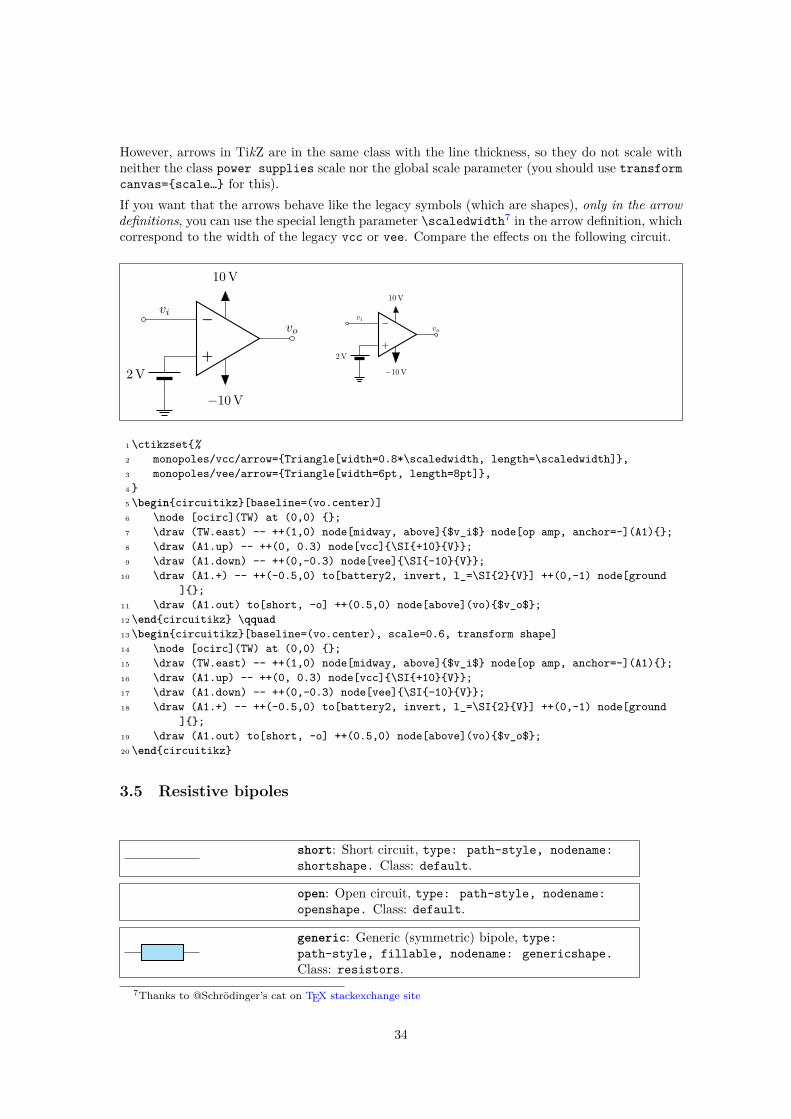
However, arrows in TikZ are in the same class with the line thickness, so they do not scale withneither the class power supplies scale nor the global scale parameter (you should use transformcanvas=scale… for this).If you want that the arrows behave like the legacy symbols (which are shapes), only in the arrowdefinitions, you can use the special length parameter \scaledwidth7 in the arrow definition, whichcorrespond to the width of the legacy vcc or vee. Compare the effects on the following circuit.
vi −
+
10 V
−10 V
2 V
vovi −
+
10 V
−10 V
2 V
vo
1 \ctikzset%2 monopoles/vcc/arrow=Triangle[width=0.8*\scaledwidth, length=\scaledwidth],3 monopoles/vee/arrow=Triangle[width=6pt, length=8pt],4 5 \begincircuitikz[baseline=(vo.center)]6 \node [ocirc](TW) at (0,0) ;7 \draw (TW.east) -- ++(1,0) node[midway, above]$v_i$ node[op amp, anchor=-](A1);8 \draw (A1.up) -- ++(0, 0.3) node[vcc]\SI+10V;9 \draw (A1.down) -- ++(0,-0.3) node[vee]\SI-10V;
10 \draw (A1.+) -- ++(-0.5,0) to[battery2, invert, l_=\SI2V] ++(0,-1) node[ground];
11 \draw (A1.out) to[short, -o] ++(0.5,0) node[above](vo)$v_o$;12 \endcircuitikz \qquad13 \begincircuitikz[baseline=(vo.center), scale=0.6, transform shape]14 \node [ocirc](TW) at (0,0) ;15 \draw (TW.east) -- ++(1,0) node[midway, above]$v_i$ node[op amp, anchor=-](A1);16 \draw (A1.up) -- ++(0, 0.3) node[vcc]\SI+10V;17 \draw (A1.down) -- ++(0,-0.3) node[vee]\SI-10V;18 \draw (A1.+) -- ++(-0.5,0) to[battery2, invert, l_=\SI2V] ++(0,-1) node[ground
];19 \draw (A1.out) to[short, -o] ++(0.5,0) node[above](vo)$v_o$;20 \endcircuitikz
3.5 Resistive bipoles
short: Short circuit, type: path-style, nodename:shortshape. Class: default.
open: Open circuit, type: path-style, nodename:openshape. Class: default.
generic: Generic (symmetric) bipole, type:path-style, fillable, nodename: genericshape.Class: resistors.
7Thanks to @Schrödinger’s cat on TEX stackexchange site
34

xgeneric: Crossed generic (symmetric) bipole, type:path-style, fillable, nodename: xgenericshape.Class: resistors.
tgeneric: Tunable generic bipole, type: path-style,fillable, nodename: tgenericshape. Class:resistors.
ageneric: Generic asymmetric bipole, type:path-style, fillable, nodename: agenericshape.Class: resistors.
memristor: Memristor, type: path-style, fillable,nodename: memristorshape.Aliases: Mr. Class:resistors.
If americanresistors option is active (or the style [american resistors] is used; this is thedefault for the package), the resistors are displayed as follows:
R: Resistor, type: path-style, nodename:resistorshape.Aliases: american resistor. Class:resistors.
vR: Variable resistor, type: path-style, nodename:vresistorshape.Aliases: variable american resistor.Class: resistors.
wiper pR: Potentiometer, type: path-style, nodename:potentiometershape.Aliases: american potentiometer.Class: resistors.
label
sR: Resisitive sensor, type: path-style, nodename:resistivesensshape.Aliases: american resisitivesensor. Class: resistors.
If instead europeanresistors option is active (or the style [european resistors] is used), theresistors, variable resistors and potentiometers are displayed as follows:
R: Resistor, type: path-style, fillable, nodename:genericshape.Aliases: european resistor. Class:resistors.
vR: Variable resistor, type: path-style, fillable,nodename: tgenericshape.Aliases: variable europeanresistor. Class: resistors.
wiper pR: Potentiometer, type: path-style, fillable,nodename: genericpotentiometershape.Aliases:european potentiometer. Class: resistors.
label
sR: Resistive sensor, type: path-style, fillable,nodename: thermistorshape.Aliases: europeanresistive sensor. Class: resistors.
Other miscellaneous resistor-like devices:
35

U
varistor: Varistor, type: path-style, fillable,nodename: varistorshape. Class: resistors.
phR: Photoresistor, type: path-style, fillable,nodename: photoresistorshape.Aliases:photoresistor. Class: resistors.
thR: Thermistor, type: path-style, fillable,nodename: thermistorshape.Aliases: thermistor.Class: resistors.
ϑ
thRp: PTC thermistor, type: path-style, fillable,nodename: thermistorptcshape.Aliases: thermistorptc. Class: resistors.
ϑ
thRn: NTC thermistor, type: path-style, fillable,nodename: thermistorntcshape.Aliases: thermistorntc. Class: resistors.
3.5.1 Potentiometers: wiper position
Since version 0.9.5, you can control the position of the wiper in potentiometers using the keywiper pos, which is a number in the range [0, 1]. The default middle position is wiper pos=0.5.
AB
C
1 \begincircuitikz[american]2 \ctikzsetresistors/width=1.5, resistors/zigs=93 \draw (0,0) to[pR, name=A] ++(0,-4);4 \draw (1.5,0) to[pR, wiper pos=0.3, name=B] ++(0,-4);5 \ctikzseteuropean resistors6 \draw (3,0) to[pR, wiper pos=0.8, name=C] ++(0,-4);7 \foreach \i in A, B, C8 \node[right] at (\i.wiper) \i;9 \endcircuitikz
3.5.2 Generic sensors anchors
Generic sensors have an extra anchor named label to help position the type of dependence, ifneeded:
R
-t°
L
C
+H%
1\begincircuitikz2 \draw (0,2) to[sR, l=$R$, name=mySR] ++(3,0);3 \node [font=\tiny, right] at(mySR.label) -t\si\degree
;4 \draw (0,0) to[sL, l=$L$, name=mySL] ++(3,0);5 \node [draw, circle, inner sep=2pt] at(mySL.label) ;6 \draw (0,-2) to[sC, l=$C$, name=mySC] ++(3,0);7 \node [font=\tiny, below right, inner sep=0pt] at(mySC.
label) +H\si\%;8\endcircuitikz
The anchor is positioned just on the corner of the segmented line crossing the component.
36

3.5.3 Resistive components customization
You can change the scale of these components (all the resistive bipoles together) by setting the keyresistors/scale (default 1.0). Similarly, you can change the widths by setting resistors/width(default 0.8).You can change the width of these components (all the resistive bipoles together) by setting thekey resistors/width to something different from the default 0.8.For the american style resistors, you can change the number of “zig-zags” by setting the keyresistors/zigs (default value 3).
R
P
R
1\begincircuitikz[2 longpot/.style = pR, resistors/scale=0.75,3 resistors/width=1.6, resistors/zigs=6]4 \draw (0,1.5) to[R, l=$R$] ++(4,0);5 \draw (0,0) to[longpot, l=$P$] ++(4,0);6 \ctikzsetresistors/scale=1.57 \draw (0,-1.5) to[R, l=$R$] ++(4,0);8\endcircuitikz
3.6 Capacitors and inductors: dynamical bipoles
3.6.1 Capacitors
capacitor: Capacitor, type: path-style, nodename:capacitorshape.Aliases: C. Class: capacitors.
curved capacitor: Curved (polarized) capacitor, type:path-style, nodename: ccapacitorshape.Aliases: cC.Class: capacitors.
+ecapacitor: Electrolytic capacitor, type: path-style,fillable, nodename: ecapacitorshape.Aliases:eC,elko. Class: capacitors.
variable capacitor: Variable capacitor, type:path-style, nodename: vcapacitorshape.Aliases: vC.Class: capacitors.
label
capacitive sensor: Capacitive sensor, type:path-style, nodename: capacitivesensshape.Aliases:sC. Class: capacitors.
piezoelectric: Piezoelectric Element, type:path-style, fillable, nodename:piezoelectricshape.Aliases: PZ. Class: capacitors.
There is also the (deprecated8 — its polarity is not coherent with the rest of the components)polar capacitor:
8Thanks to Anshul Singhv for noticing.
37

polar capacitor: Polar capacitor, type: path-style,nodename: pcapacitorshape.Aliases: pC. Class:capacitors.
3.6.2 Capacitive sensors anchors
For capacitive sensors, see section 3.5.2.
3.6.3 Capacitors customizations
You can change the scale of the capacitors by setting the key capacitors/scale to somethingdifferent from the default 1.0.
3.6.4 Inductors
If the cuteinductors option is active (default behaviour), or the style [cute inductors] is used,the inductors are displayed as follows:
midtap L: Inductor, type: path-style, nodename:cuteinductorshape.Aliases: cute inductor. Class:inductors.
cute choke: Choke, type: path-style, nodename:cutechokeshape. Class: inductors.
vL: Variable inductor, type: path-style, nodename:vcuteinductorshape.Aliases: variable cute inductor.Class: inductors.
label
sL: Inductive sensor, type: path-style, nodename:scuteinductorshape.Aliases: cute inductive sensor.Class: inductors.
If the americaninductors option is active (or the style [american inductors] is used), theinductors are displayed as follows:
midtap L: Inductor, type: path-style, nodename:americaninductorshape.Aliases: american inductor.Class: inductors.
vL: Variable inductor, type: path-style, nodename:vamericaninductorshape.Aliases: variable americaninductor. Class: inductors.
label
sL: Inductive sensor, type: path-style, nodename:samericaninductorshape.Aliases: american inductivesensor. Class: inductors.
Finally, if the europeaninductors option is active (or the style [european inductors] is used),the inductors are displayed as follows:
38

midtap L: Inductor, type: path-style, nodename:fullgenericshape.Aliases: european inductor. Class:inductors.
vL: Variable inductor, type: path-style, nodename:tfullgenericshape.Aliases: variable europeaninductor. Class: inductors.
label
sL: Inductive sensor, type: path-style, nodename:sfullgenericshape.Aliases: european inductivesensor. Class: inductors.
3.6.5 Inductors customizations
You can change the scale of the inductors by setting the key inductors/scale to somethingdifferent from the default 1.0.You can change the width of these components (all the inductors together, unless you use styleor scoping) by setting the key inductors/width to something different from the default, which is0.8 for american and european inductors, and 0.6 for cute inductors.Moreover, you can change the number of “coils” drawn by setting the key inductors/coils(default value 5 for cute inductors and 4 for american ones). Notice that the minimum numberof coils is 1 for american inductors, and 2 for cute ones.
L
L
L
1\begincircuitikz[2 longL/.style = cute choke, inductors/scale
=0.75,3 inductors/width=1.6, inductors/coils=9]4 \draw (0,1.5) to[L, l=$L$] ++(4,0);5 \draw (0,0) to[longL, l=$L$] ++(4,0);6 \ctikzsetinductors/scale=1.5, inductor=american7 \draw (0,-1.5) to[L, l=$L$] ++(4,0);8\endcircuitikz
Chokes (which comes only in the cute style) can have single and double lines, and can have theline thickness adjust (the value is relative to the thickness of the inductor).
1\begincircuitikz[american]2 \draw (0,0) to[cute choke] ++(3,0);3 \draw (0,-1) to[cute choke, twolineschoke] ++(3,0);4
5 \ctikzsetbipoles/cutechoke/cthick=2, twolineschoke6
7 \draw (0,-2) to[cute choke] ++(3,0);8 \draw (0,-3) to[cute choke, onelinechoke] ++(3,0);9\endcircuitikz
39

3.6.6 Inductors anchors
For inductive sensors, see section 3.5.2.Inductors have an additional anchor, called midtap, that connects to the center of the coil “wire”.Notice that this anchor could be on one side or the other of the component, depending on thenumber of loops of the element; if you need a fixed position, you can use the geographical anchors.
1 \begincircuitikz[2 loops/.style=circuitikz/inductors/coils=#1]3 \ctikzsetcute inductors4 \draw (0,2) to[L, loops=5, name=A] ++(2,0)5 to[L, loops=6, name=B] ++(2,0);6 \ctikzsetamerican inductors7 \draw (0,0) to[L, loops=5, name=C] ++(2,0)8 to[L, loops=6, name=D] ++(2,0);9 \foreach \i in A, B, C, D
10 \node[circle, fill=red, inner sep=1pt] at (\i.midtap);11 \endcircuitikz
3.7 Diodes and such
There are three basic styles for diodes: empty (fillable in color), full (completely filled with thedraw color) and stroke (empty, but with a line across them).You can switch between the styles setting the key diode (for example \ctikzsetdiode=fullor empty or stroke, or with the styles full diodes, empty diodes and stroke diodes.To use the default element, simply use the name shown for the empty diodes without the final “o”— that is D, sD, and so on. The names shown in the following tables will draw the specified diodeindependently on the style chosen (that is, leD* is always a full LED diode).
The package options fulldiode, strokediode, and emptydiode (and the styles [fulldiodes], [stroke diodes], and [empty diodes]) define which shape will be used by ab-breviated commands such that D, sD, zD, zzD, tD, pD, leD, VC, Ty,Tr (no stroke symbolavailable!).
empty diode: Empty diode, type: path-style,fillable, nodename: emptydiodeshape.Aliases: Do.Class: diodes.
empty Schottky diode: Empty Schottky diode, type:path-style, fillable, nodename:emptysdiodeshape.Aliases: sDo. Class: diodes.
empty Zener diode: Empty Zener diode, type:path-style, fillable, nodename:emptyzdiodeshape.Aliases: zDo. Class: diodes.
empty ZZener diode: Empty ZZener diode, type:path-style, fillable, nodename:emptyzzdiodeshape.Aliases: zzDo. Class: diodes.
40

empty tunnel diode: Empty tunnel diode, type:path-style, fillable, nodename:emptytdiodeshape.Aliases: tDo. Class: diodes.
empty photodiode: Empty photodiode, type:path-style, fillable, nodename:emptypdiodeshape.Aliases: pDo. Class: diodes.
empty led: Empty led, type: path-style, fillable,nodename: emptylediodeshape.Aliases: leDo. Class:diodes.
empty varcap: Empty varcap, type: path-style,fillable, nodename: emptyvarcapshape.Aliases: VCo.Class: diodes.
empty bidirectionaldiode: Empty bidirectionaldiode,type: path-style, fillable, nodename:emptybidirectionaldiodeshape.Aliases: biDo. Class:diodes.
full diode: Full diode, type: path-style, nodename:fulldiodeshape.Aliases: D*. Class: diodes.
full Schottky diode: Full Schottky diode, type:path-style, nodename: fullsdiodeshape.Aliases:sD*. Class: diodes.
full Zener diode: Full Zener diode, type:path-style, nodename: fullzdiodeshape.Aliases:zD*. Class: diodes.
full ZZener diode: Full ZZener diode, type:path-style, nodename: fullzzdiodeshape.Aliases:zzD*. Class: diodes.
full tunnel diode: Full tunnel diode, type:path-style, nodename: fulltdiodeshape.Aliases:tD*. Class: diodes.
full photodiode: Full photodiode, type: path-style,nodename: fullpdiodeshape.Aliases: pD*. Class:diodes.
full led: Full led, type: path-style, nodename:fulllediodeshape.Aliases: leD*. Class: diodes.
full varcap: Full varcap, type: path-style,nodename: fullvarcapshape.Aliases: VC*. Class:diodes.
full bidirectionaldiode: Full bidirectionaldiode,type: path-style, nodename:fullbidirectionaldiodeshape.Aliases: biD*. Class:diodes.
These shapes have no exact node-style counterpart, because the stroke line is built upon the emptyvariants:
41

stroke diode: Stroke diode, type: path-style,fillable, nodename: emptydiodeshape.Aliases: D-.Class: diodes.
stroke Schottky diode: Stroke Schottky diode, type:path-style, fillable, nodename:emptysdiodeshape.Aliases: sD-. Class: diodes.
stroke Zener diode: Stroke Zener diode, type:path-style, fillable, nodename:emptyzdiodeshape.Aliases: zD-. Class: diodes.
stroke ZZener diode: Stroke ZZener diode, type:path-style, fillable, nodename:emptyzzdiodeshape.Aliases: zzD-. Class: diodes.
stroke tunnel diode: Stroke tunnel diode, type:path-style, fillable, nodename:emptytdiodeshape.Aliases: tD-. Class: diodes.
stroke photodiode: Stroke photodiode, type:path-style, fillable, nodename:emptypdiodeshape.Aliases: pD-. Class: diodes.
stroke led: Stroke led, type: path-style, fillable,nodename: emptylediodeshape.Aliases: leD-. Class:diodes.
stroke varcap: Stroke varcap, type: path-style,fillable, nodename: emptyvarcapshape.Aliases: VC-.Class: diodes.
3.7.1 Tripole-like diodes
The following tripoles are entered with the usual command, of the form to[Tr, …].
G
anode cathode
triac: Standard triac (shape depends on package option),type: path-style, fillable, nodename:emptytriacshape.Aliases: Tr. Class: diodes.
gateempty triac: Empty triac, type: path-style,fillable, nodename: emptytriacshape.Aliases: Tro.Class: diodes.
full triac: Full triac, type: path-style, nodename:fulltriacshape.Aliases: Tr*. Class: diodes.
42

G
anode cathode
thyristor: Standard thyristor (shape depends onpackage option), type: path-style, fillable,nodename: emptythyristorshape.Aliases: Ty. Class:diodes.
empty thyristor: Empty thyristor, type: path-style,fillable, nodename: emptythyristorshape.Aliases:Tyo. Class: diodes.
full thyristor: Full thyristor, type: path-style,nodename: fullthyristorshape.Aliases: Ty*. Class:diodes.
stroke thyristor: Stroke thyristor, type: path-style,fillable, nodename: emptythyristorshape.Aliases:Ty-. Class: diodes.
3.7.2 Triacs anchors
When inserting a thrystor, a triac or a potentiometer, one needs to refer to the third node-gate(gate or G) for the former two; wiper (wiper or W) for the latter one. This is done by giving aname to the bipole:
1\begincircuitikz \draw2 (0,0) to[Tr, n=TRI] (2,0)3 to[pR, n=POT] (4,0);4 \draw[dashed] (TRI.G) -| (POT.wiper)5;\endcircuitikz
3.7.3 Diode customizations
You can change the scale of the diodes by setting the key diodes/scale to something differentfrom the default 1.0. In Romano’s opinion, diodes are somewhat big with the default style of thepackage, so a setting like \ctikzsetdiode/scale=0.6 is recommended.
D
D
1\begincircuitikz2 \draw (0,1) to[D, l=$D$] ++(2,0)3 node[npn, anchor=B];4 \ctikzsetdiodes/scale=0.65 \draw (0,-1) to[D, l=$D$] ++(2,0)6 node[npn, anchor=B];7\endcircuitikz
You can change the direction of the LEDs and photodiodes’ arrows by using the binary keys ledarrows from cathode and pd arrows to cathode (the default are led arrows from anode andpd arrows to anode), as you can see in the following example.
43

1 \begincircuitikz2 \ctikzsetled arrows from anode % default3 \ctikzsetpd arrows to anode % default4 \ctikzsetfull diodes5 \draw (0,0) to[leD] ++(1.5,0) to[pD] ++(1.5,0);6 \ctikzsetstroke diodes7 \draw (0,-1) to[leD] ++(1.5,0) to[pD] ++(1.5,0);8 \ctikzsetempty diodes9 \draw (0,-2) to[leD] ++(1.5,0) to[pD] ++(1.5,0);
10
11 \ctikzsetled arrows from cathode12 \ctikzsetpd arrows to cathode13 \ctikzsetfull diodes14 \draw (0,-4) to[leD] ++(1.5,0) to[pD] ++(1.5,0);15 \ctikzsetstroke diodes16 \draw (0,-5) to[leD] ++(1.5,0) to[pD] ++(1.5,0);17 \ctikzsetempty diodes18 \draw (0,-6) to[leD] ++(1.5,0) to[pD] ++(1.5,0);19 \endcircuitikz
3.8 Sources and generators
Notice that source and generators are divided in three classes that can be styled independently:traditional battery symbols (class batteries), independent generators (class sources) and de-pendent generators (class csources). This is because they are often treated differently, and soyou can choose to, for example, fill the dependent sources but not the independent ones.
3.8.1 Batteries
battery: Battery, type: path-style, nodename:batteryshape. Class: batteries.
battery1: Single battery cell, type: path-style,nodename: battery1shape. Class: batteries.
battery2: Single battery cell, type: path-style,nodename: battery2shape. Class: batteries.
3.8.2 Stationary sources
european voltage source: Voltage source (europeanstyle), type: path-style, fillable, nodename:vsourceshape. Class: sources.
cute european voltage source: Voltage source (cuteeuropean style), type: path-style, fillable,nodename: vsourceCshape.Aliases: vsourceC, ceV.Class: sources.
44

+−american voltage source: Voltage source (americanstyle), type: path-style, fillable, nodename:vsourceAMshape. Class: sources.
european current source: Current source (europeanstyle), type: path-style, fillable, nodename:isourceshape. Class: sources.
cute european current source: Current source (cuteeuropean style), type: path-style, fillable,nodename: isourceCshape.Aliases: isourceC, ceI.Class: sources.
american current source: Current source (americanstyle), type: path-style, fillable, nodename:isourceAMshape. Class: sources.
If (default behaviour) europeancurrents option is active (or the style [european currents]is used), the shorthands current source, isource, and I are equivalent to europeancurrent source. Otherwise, if americancurrents option is active (or the style [americancurrents] is used) they are equivalent to american current source.Similarly, if (default behaviour) europeanvoltages option is active (or the style [europeanvoltages] is used), the shorthands voltage source, vsource, and V are equivalent toeuropean voltage source. Otherwise, if americanvoltages option is active (or the style[american voltages] is used) they are equivalent to american voltage source.
3.8.3 Sinusoidal sources
These two are basically the same symbol; to distinguish among them, you have to add a label,which will be a voltage or a current.
sinusoidal voltage source: Sinusoidal voltage source,type: path-style, fillable, nodename:vsourcesinshape.Aliases: vsourcesin, sV. Class:sources.
sinusoidal current source: Sinusoidal current source,type: path-style, fillable, nodename:isourcesinshape.Aliases: isourcesin, sI. Class:sources.
− +V
I
1\begincircuitikz[american]2 \draw (0,1) to[sV=$V$] ++(3,0);3 \draw (0,0) to[sI=$I$] ++(3,0);4\endcircuitikz
45

3.8.4 Controlled sources
european controlled voltage source: Controlledvoltage source (european style), type: path-style,fillable, nodename: cvsourceshape. Class:csources.
cute european controlled voltage source: Voltagesource (cute european style), type: path-style,fillable, nodename: cvsourceCshape.Aliases:cvsourceC, cceV. Class: csources.
+−
american controlled voltage source: Controlledvoltage source (american style), type: path-style,fillable, nodename: cvsourceAMshape. Class:csources.
european controlled current source: Controlledcurrent source (european style), type: path-style,fillable, nodename: cisourceshape. Class:csources.
cute european controlled current source: Currentsource (cute european style), type: path-style,fillable, nodename: cisourceCshape.Aliases:cisourceC, cceI. Class: csources.
american controlled current source: Controlledcurrent source (american style), type: path-style,fillable, nodename: cisourceAMshape. Class:csources.
empty controlled source: Empty controlled source,type: path-style, fillable, nodename:ecsourceshape.Aliases: ecsource. Class: csources.
If (default behaviour) europeancurrents option is active (or the style [european currents]is used), the shorthands controlled current source, cisource, and cI are equivalent toeuropean controlled current source. Otherwise, if americancurrents option is active(or the style [american currents] is used) they are equivalent to american controlledcurrent source.Similarly, if (default behaviour) europeanvoltages option is active (or the style [europeanvoltages] is used), the shorthands controlled voltage source, cvsource, and cV areequivalent to european controlled voltage source. Otherwise, if americanvoltages op-tion is active (or the style [american voltages] is used) they are equivalent to americancontrolled voltage source.
The following two behave like the corresponding independent sources, see section 3.8.3.
46
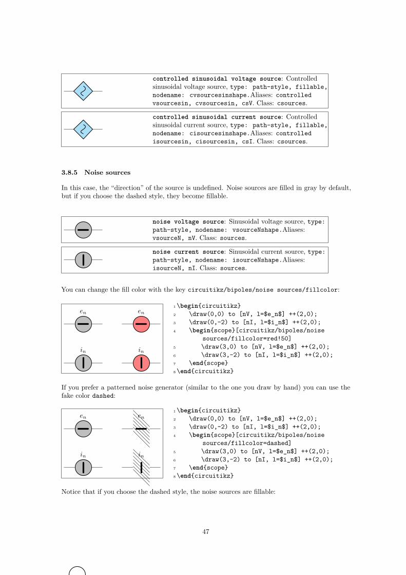
controlled sinusoidal voltage source: Controlledsinusoidal voltage source, type: path-style, fillable,nodename: cvsourcesinshape.Aliases: controlledvsourcesin, cvsourcesin, csV. Class: csources.
controlled sinusoidal current source: Controlledsinusoidal current source, type: path-style, fillable,nodename: cisourcesinshape.Aliases: controlledisourcesin, cisourcesin, csI. Class: csources.
3.8.5 Noise sources
In this case, the “direction” of the source is undefined. Noise sources are filled in gray by default,but if you choose the dashed style, they become fillable.
noise voltage source: Sinusoidal voltage source, type:path-style, nodename: vsourceNshape.Aliases:vsourceN, nV. Class: sources.
noise current source: Sinusoidal current source, type:path-style, nodename: isourceNshape.Aliases:isourceN, nI. Class: sources.
You can change the fill color with the key circuitikz/bipoles/noise sources/fillcolor:
en
in
en
in
1\begincircuitikz2 \draw(0,0) to [nV, l=$e_n$] ++(2,0);3 \draw(0,-2) to [nI, l=$i_n$] ++(2,0);4 \beginscope[circuitikz/bipoles/noise
sources/fillcolor=red!50]5 \draw(3,0) to [nV, l=$e_n$] ++(2,0);6 \draw(3,-2) to [nI, l=$i_n$] ++(2,0);7 \endscope8\endcircuitikz
If you prefer a patterned noise generator (similar to the one you draw by hand) you can use thefake color dashed:
en
in
en
in
1\begincircuitikz2 \draw(0,0) to [nV, l=$e_n$] ++(2,0);3 \draw(0,-2) to [nI, l=$i_n$] ++(2,0);4 \beginscope[circuitikz/bipoles/noise
sources/fillcolor=dashed]5 \draw(3,0) to [nV, l=$e_n$] ++(2,0);6 \draw(3,-2) to [nI, l=$i_n$] ++(2,0);7 \endscope8\endcircuitikz
Notice that if you choose the dashed style, the noise sources are fillable:
47

en
in
en
in
1\begincircuitikz2 \ctikzsetbipoles/noise sources/fillcolor=
dashed3 \draw(0,0) to [nV, l=$e_n$] ++(2,0);4 \draw(0,-2) to [nI, l=$i_n$] ++(2,0);5 \beginscope6 \draw(3,0) to [nV, l=$e_n$, fill=yellow
!50!red] ++(2,0);7 \draw(3,-2) to [nI, l=$i_n$, fill=blue
!50!white] ++(2,0);8 \endscope9\endcircuitikz
3.8.6 Special sources
square voltage source: Square voltage source, type:path-style, fillable, nodename:vsourcesquareshape.Aliases: vsourcesquare, sqV.Class: sources.
vsourcetri: Triangle voltage source, type: path-style,fillable, nodename: vsourcetrishape.Aliases: tV.Class: sources.
esource: Empty voltage source, type: path-style,fillable, nodename: esourceshape. Class: sources.
pvsource: Photovoltaic-voltage source, type:path-style, fillable, nodename: pvsourceshape.Class: sources.
ioosource: Double Zero style current source, type:path-style, fillable, nodename: oosourceshape.Class: sources.
voosource: Double Zero style voltage source, type:path-style, fillable, nodename: oosourceshape.Class: sources.
3.8.7 DC sources
dcvsource: DC voltage source, type: path-style,fillable, nodename: dcvsourceshape. Class:sources.
dcisource: DC current source, type: path-style,fillable, nodename: dcisourceshape. Class:sources.
The size of the broken part of the DC current source is configurable by changing the value ofbipoles/dcisource/angle (default 80); values must be between 0 (no circle at all, probably notuseful) and 90 (full circle, again not useful).
48

1\begincircuitikz2 \draw (0,0) to[dcvsource] ++(2,0)3 to [dcisource, fill=yellow] ++(2,0) ;4 \ctikzsetbipoles/dcisource/angle=455 \draw (0,-2) to[dcvsource] ++(2,0)6 to [dcisource, fill=yellow] ++(2,0) ;7\endcircuitikz
3.8.8 Sources customizations
You can change the scale of the batteries by setting the key batteries/scale, for the controlled(dependent) sources with csources/scale, and for all the other independent sources and genera-tors with sources/scale, to something different from the default 1.0.
3.9 Instruments
A ammeter: Ammeter, type: path-style, fillable,nodename: ammetershape. Class: instruments.
V voltmeter: Voltmeter, type: path-style, fillable,nodename: voltmetershape. Class: instruments.
Ωohmmeter: Ohmmeter, type: path-style, fillable,nodename: ohmmetershape. Class: instruments.
left right
center
rmeter: Round meter (use t=... for the symbol), type:path-style, fillable, nodename: rmetershape.Class: instruments.
left right
center
rmeterwa: Round meter with arrow (use t=... for thesymbol), type: path-style, fillable, nodename:rmeterwashape. Class: instruments.
left right
centerin 1 in 2
smeter: Square meter (use t=... for the symbol), type:path-style, fillable, nodename: smetershape.Class: instruments.
left right
center
qiprobe: QUCS-style current probe, type: path-style,fillable, nodename: qiprobeshape. Class:instruments.
left right
center
qvprobe: QUCS-style voltage probe, type: path-style,fillable, nodename: qvprobeshape. Class:instruments.
left right
centerv+ v-
qpprobe: QUCS-style power probe, type: path-style,fillable, nodename: qpprobeshape. Class:instruments.
49
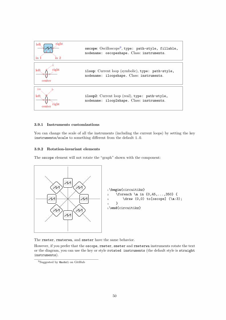
left right
in 1 in 2
oscope: Oscilloscope9, type: path-style, fillable,nodename: oscopeshape. Class: instruments.
left right
center
i
iloop: Current loop (symbolic), type: path-style,nodename: iloopshape. Class: instruments.
left
rightcenter
i+ i-
iloop2: Current loop (real), type: path-style,nodename: iloop2shape. Class: instruments.
3.9.1 Instruments customizations
You can change the scale of all the instruments (including the current loops) by setting the keyinstruments/scale to something different from the default 1.0.
3.9.2 Rotation-invariant elements
The oscope element will not rotate the “graph” shown with the component:
1\begincircuitikz2 \foreach \a in 0,45,...,350 3 \draw (0,0) to[oscope] (\a:3);4 5\endcircuitikz
The rmeter, rmaterwa, and smeter have the same behavior.However, if you prefer that the oscope, rmeter, smeter and rmeterwa instruments rotate the textor the diagram, you can use the key or style rotated instruments (the default style is straightinstruments).
9Suggested by @nobrl on GitHub
50

A
A
A A
1 \begincircuitikz[scale=0.8, transform shape]2 \ctikzsetrotated instruments % new default3 \draw (0,0) to[oscope] ++(0:3);4 \draw (0,0) to[oscope] ++(60:3);5 \draw (0,0) to[rmeter, t=A] ++(120:3);6 % local override7 \draw (0,0) to[rmeterwa, t=A, straight instruments]
++(180:3);8 \ctikzsetstraight instruments % back to default9 \draw (0,0) to[rmeterwa, t=A] ++(240:3);
10 % local override11 \draw (0,0) to[smeter, t=A, rotated instruments]
++(300:3);12 \endcircuitikz
3.9.3 Instruments as node elements
The node-style usage of the oscope is also interesting, using the additional in 1 and in 2 an-chors; notice that in this case you can use the text content of the node to put labels above it.Moreover, you can change the size of the oscilloscope by changing bipoles/oscope/width andbipoles/oscope/height keys (which both default to 0.6).
C1
C2
1\begincircuitikz2 \draw (0,1)3 to[oscope=$C_1$, fill=green!20!gray, name=O1] ++(2,0);4 \path (O1.right)5 node[ground, scale=0.5, below right=4pt];6 \ctikzsetbipoles/oscope/width=1.07 \draw (1,-1)8 node[oscopeshape, fill=yellow!20!orange](O2)$C_2$;9 \draw (O2.in 2) to[short, *-] ++(0,-0.5) node[ground];
10 \draw (O2.in 1) to[short, *-] ++(0,-0.5)11 -- ++(-1,0) node[currarrow, xscale=-1];12\endcircuitikz
3.9.4 Measuring voltage and currents, multiple ways
This is the classical (legacy) option, with the voltmeter and ammeter. The problem is thatelements are intrinsically horizontal, so they look funny if put in vertically.
AV
1\begincircuitikz2 \draw (0,0) -- ++(1,0) to[R] ++(2,0)3 to [ammeter] ++(0,-2) node[ground];4 \draw (1,0) to[voltmeter] ++(0,-2)5 node[ground];6\endcircuitikz
So the solution is often changing the structure to keep the meters in horizontal position.
51

A
V 1\begincircuitikz2 \draw (0,0) -- ++(1,0) to[R] ++(2,0)3 to [ammeter] ++(2,0) --4 ++(0,-1) node[ground];5 \draw (1,0) -- (1,1) to[voltmeter]6 ++(2,0) node[ground];7\endcircuitikz
Since version 0.9.0 you have more options for the measuring instruments. You can use the genericrmeterwa (round meter with arrow), to which you can specify the internal symbol with the optiont=... (and is fillable).
A
i
V
+
−
v
1 \begincircuitikz[american]2 \draw (0,0) -- ++(1,0) to[R] ++(2,0)3 to [rmeterwa, t=A, i=$i$] ++(0,-2) node[ground];4 \draw (1,0) to[rmeterwa, t=V, v=$v$] ++(0,-2)5 node[ground];6\endcircuitikz
This kind of component will keep the symbol horizontal, whatever the orientation:
Ai
V+ −
v 1 \begincircuitikz[american]2 \draw (0,0) -- ++(1,0) to[R] ++(2,0)3 to [rmeterwa, t=A, i=$i$] ++(2,0) --4 ++(0,-1) node[ground];5 \draw (1,0) -- (1,1) to[rmeterwa, t=V, v^=$v
$]6 ++(2,0) node[ground];7\endcircuitikz
The plain rmeter is the same, without the measuring arrow:
A
i
V
+
−
v
1\begincircuitikz[american]2 \draw (0,0) -- ++(1,0) to[R] ++(2,0)3 to [rmeter, t=A, i=$i$] ++(0,-2) node[ground];4 \draw (1,0) to[rmeter, t=V, v=$v$] ++(0,-2)5 node[ground];6\endcircuitikz
If you prefer it, you have the option to use square meters, in order to have more visual differencefrom generators:
Ai
V
+
−
v
1\begincircuitikz[american]2 \draw (0,0) -- ++(1,0) to[R] ++(2,0)3 to [smeter, t=A, i=$i$] ++(0,-2) node[ground];4 \draw (1,0) to[smeter, t=V, v=$v$] ++(0,-2)5 node[ground];6\endcircuitikz
52

Another possibility is to use QUCS10-style probes, which have the nice property of explictlyshowing the type of connection (in series or parallel) of the meter:
iv
1\begincircuitikz[american]2 \draw (0,0) -- ++(1,0) to[R] ++(2,0)3 to [qiprobe, l=$i$] ++(0,-2) node[ground];4 \draw (1,0) to[qvprobe, l=$v$] ++(0,-2)5 node[ground];6\endcircuitikz
If you want to explicitly show a power measurement, you can use the power probe qpprobe andusing the additional anchors v+ and v- :
iv
1\begincircuitikz[american]2 \draw (0,0) to[short,-*] ++(1,0) coordinate(b)3 to[R] ++(2,0) to [qpprobe, l=$i$, a=$v$, name=P]4 ++(0,-2.5) node[ground](GND);5 \draw (P.v-) -| ++(-0.5,-1) coordinate(a)6 to [short, -*] (a-|GND);7 \draw (P.v+) -| (b);8\endcircuitikz
The final possibility is to use oscilloscopes. For example:
+
−
v
1\begincircuitikz[american]2 \draw (0,0) -- ++(1,0) to[R] ++(3,0)3 to [iloop, mirror, name=I] ++(0,-2)4 node[ground] (GND);5 \draw (1,0) to[oscope, v=$v$] ++(0,-2)6 node[ground];7 \draw (I.i) -- ++(-0.5,0) node[oscopeshape,
anchor=right, name=O];8 \draw (O.south) -- (O.south |- GND) node[
ground];9\endcircuitikz
Or, if you want a more physical structure for the measurement setup:
10QUCS is an open source circuit simulator: http://qucs.sourceforge.net/
53

1\begincircuitikz[american]2 \draw (0,0) -- ++(1,0) to[R] ++(3,0) to [iloop2, name=I] ++(0,-2)3 node[ground] (GND);4 \ctikzsetbipoles/oscope/width=1.6\ctikzsetbipoles/oscope/height=1.25 \node [oscopeshape, fill=green!10](O) at (6,2);6 \node [bnc, xscale=-1, anchor=zero](bnc1) at (O.in 1);7 \node [bnc, , anchor=zero, rotate=-90](bnc2) at (O.in 2);8 \draw [-latexslim] (bnc1.hot) -| (1,0);9 \draw (bnc2.hot) |- (I.i+);
10 \draw (I.i-) node[ground, scale=0.5];11\endcircuitikz
3.10 Mechanical Analogy
damper: Mechanical Damping, type: path-style,fillable, nodename: dampershape. Class:mechanicals.
spring: Mechanical Stiffness, type: path-style,nodename: springshape. Class: mechanicals.
left right
center
viscoe: Mechanical viscoelastic element11, type:path-style, fillable, nodename: viscoeshape.Class: mechanicals.
mass: Mechanical Mass, type: path-style, fillable,nodename: massshape. Class: mechanicals.
3.10.1 Mechanical elements customizations
You can change the scale of all the mechanical elements by setting the key mechanicals/scaleto something different from the default 1.0.
11Suggested by @Alex in https://tex.stackexchange.com/q/484268/38080
54

3.11 Miscellaneous bipoles
Here you’ll find bipoles that are not easily grouped in the categories above.
thermocouple: Thermocouple, type: path-style,nodename: thermocoupleshape. Class: misc.
fuse: Fuse, type: path-style, fillable, nodename:fuseshape. Class: misc.
afuse: Asymmetric fuse, type: path-style, fillable,nodename: afuseshape.Aliases: asymmetric fuse.Class: misc.
squid: Squid, type: path-style, nodename:squidshape. Class: misc.
barrier: Barrier, type: path-style, nodename:barriershape. Class: misc.
openbarrier: Open barrier, type: path-style,nodename: openbarriershape. Class: misc.
You can tune how big is the gap in the openbarrier component by setting the key bipoles/openbarrier/gap(default value 0.5; 0 means no gap and 1 full gap).
european gas filled surge arrester: European gasfilled surge arrester, type: path-style, fillable,nodename: european gas filled surgearrestershape. Class: misc.
american gas filled surge arrester: American gasfilled surge arrester, type: path-style, fillable,nodename: american gas filled surgearrestershape. Class: misc.
If (default behaviour) europeangfsurgearrester option is active (or the style [europeangas filled surge arrester] is used), the shorthands gas filled surge arrester andgf surge arrester are equivalent to the european version of the component.If otherwise americangfsurgearrester option is active (or the style [american gas filledsurge arrester] is used), the shorthands the shorthands gas filled surge arrester andgf surge arrester are equivalent to the american version of the component.
lamp: Lamp, type: path-style, fillable, nodename:lampshape. Class: misc.
55

bulb: Bulb, type: path-style, fillable, nodename:bulbshape. Class: misc.
north north east
east
south eastsouthsouth west
west
north west
left right
center
loudspeaker: loudspeaker, type: path-style,fillable, nodename: loudspeakershape. Class: misc.
north north east
east
south eastsouthsouth west
west
north west
left right
center
mic: mic, type: path-style, fillable, nodename:micshape. Class: misc.
You can use microphones and loudspeakers with waves (see section 3.19) too:
A
1 \begincircuitikz2 \draw (0,0) to[mic, name=M] ++(0,2)3 to[amp, t=$A$] ++(2,0)4 to[loudspeaker, name=L] ++(0,-2)5 to[short, -*] (0,0) node[ground];6 \node [waves, scale=0.7, left=5pt]7 at(M.north) ;8 \node [waves, scale=0.7, right]9 at(L.north) ;
10 \endcircuitikz
3.11.1 Miscellanous element customization
You can change the scale of all the miscellaneous elements by setting the key misc/scale tosomething different from the default 1.0.
3.12 Multiple wires (buses)
This are simple drawings to indicate multiple wires.
multiwire: Single line multiple wires, type:path-style, nodename: multiwireshape.Aliases:multiwire. Class: default.
bmultiwire: Double line multiple wires, type:path-style, nodename: bmultiwireshape.Aliases:bmultiwire. Class: default.
56

4
6
1\begincircuitikz2 \draw (0,0) to[multiwire=4] ++(1,0);3 \draw (0,-2) to[bmultiwire=6] ++(1,0);4\endcircuitikz
3.13 Crossings
Path style:
crossing: Jumper style non-contact crossing, type:path-style, nodename: crossingshape.Aliases: xing.Class: default.
Node style:
Jumper-style crossing node, type: node (node[jumpcrossing]). No class.
Plain style crossing node, type: node (node[plaincrossing]). No class.
All circuit-drawing standards agree that to show a crossing without electric contact, a simplecrossing of the wires suffices; the electrical contact must be explicitly marked with a filled dot.
1\begincircuitikz[]2\draw(1,-1) to[short] (1,1)3 (0,0) to[short] (2,0);4\draw(4,-1) to[short] (4,1)5 (3,0) to[short] (5,0)6 (4,0) node[circ];7\endcircuitikz
However, sometime it is advisable to mark the non-contact situation more explicitly. To this end,you can use a path-style component called crossing:
1\begincircuitikz[]2\draw(1,-1) to[short] (1,1) (0,0) to[crossing]
(2,0);3\draw(4,-1) to[short] (4,1) (3,0) to[short]
(5,0)4 (4,0) node[circ];5\endcircuitikz
That should suffice most of the time; the only problem is that the crossing jumper will be put inthe center of the subpath where the to[crossing] is issued, so sometime a bit of trial and erroris needed to position it.For a more powerful (and elegant) way you can use the crossing nodes:
57

1\begincircuitikz[]2 \node at (1,1)[jump crossing](X);3 \draw (X.west) -- ++(-1,0);4 \draw (X.east) to[R] ++(2,0);5 \draw (X.north) node[vcc];6 \draw (X.south) to[C] ++(0,-1.5);7\endcircuitikz
Notice that the plain crossing and the jump crossing have a small gap in the straight wire,to enhance the effect of crossing (as a kind of shadow).The size of the crossing elements can be changed with the key bipoles/crossing/size (default0.2).
3.14 Arrows
These are pseudo-arrows used in lot of places in the packages (for transistors, flows, currents, andso on). The first three arrows are magnified by a factor 3 in the boxes below; for the trarrow, theanchor tip is exactly on the tip and btip is slightly receded.
center Arrow for current and voltage, type: node(node[currarrow]). No class.
center Arrow that is anchored at its tip, useful for blockdiagrams., type: node (node[inputarrow]). No class.
centertip
btip
Arrow the same size of currarrow but only filled., type:node (node[trarrow]). No class.
Ip
centereastwest
text Arrow used for the flows, with a text anchor, type: node(node[flowarrow]$I_p$). No class.
3.14.1 Arrows size
You can use the parameter current arrow scale to change the size of the arrows in variouscomponents and indicators; the normal value is 16, higher numbers give smaller arrows and so on.You need to use circuitikz/current arrow scale if you use it into a node.
f
f
f
1\begincircuitikz2 \draw (0,0) to[R, i=f] ++(2,0) node[npn, anchor=B];3 \draw (0,-2) to[R, f=f, current arrow scale=8] ++(2,0)4 node[pnp, anchor=B, circuitikz/current arrow scale
=8];5 \draw (0,-4) to[R, f=f, current arrow scale=24] ++(2,0)6 node[nigbt, anchor=B];7\endcircuitikz
58

Moreover, you have the arrow tip latexslim which is an arrow similar to the old (in deprecatedarrows library) latex' element:
1\begincircuitikz[american,]2 \draw [latexslim-latexslim] (0,0) -- (1,0);3\endcircuitikz
3.15 Terminal shapes
These are the so-called “bipole nodes” shapes, or poles (see section 5.1). These nodes are alwaysfilled; the “open” versions (starting with an o) are by default filled white, but you can override itwith the fill parameter.
Connected terminal, type: node (node[circ]). Noclass.
Unconnected terminal, type: node (node[ocirc]). Noclass.
Diamond-square terminal, type: node(node[diamondpole]). No class.
Open diamond-square terminal, type: node(node[odiamondpole]). No class.
Square-shape terminal, type: node(node[squarepole]). No class.
Open square-shape terminal, type: node(node[osquarepole]). No class.
Since version 0.9.0, “bipole nodes” shapes have all the standard geographical anchors, so you cando things like these:
R
1\begincircuitikz[american,]2 \draw (0,-1) node[draw](R)R;3 \draw (R.east) node[ocirc, right];4\endcircuitikz
The size of the poles is controlled by the key nodes width (default 0.04, relative to the basiclength). Be sure to see section 5.1 for more usage and configurability.
59

3.15.1 BNC connector/terminal
left right
center
hot
zero
BNC connector, type: node, fillable (node[bnc]). Noclass.
The BNC connector is defined so that you can easily connect it as input or output (but rememberthat you need to flip the text if you flip the component):
vi 50Ω vo
1\begincircuitikz2 \draw (0,0)3 node[bnc](B1)$v_i$ to[R=\SI50\ohm] ++(3,0)4 node[bnc, xscale=-1](B2)\scalebox-1[1]$v_o$;5 \node [ground] at (B1.shield) ;6 \node [eground] at (B2.shield);7\endcircuitikz
It also has a zero anchor if you need to rotate it about its real center.
1\begincircuitikz2 \draw[thin, red] (0,0) -- ++(1,0) (0,-1) -- ++(1,0);3 \path (0,0) node[bnc] ++(1,0) node[bnc, rotate=-90];4 \path (0,-1) node[bnc, anchor=zero] ++(1,0) node[bnc, anchor=
zero, rotate=-90];5\endcircuitikz
3.16 Block diagram components
Contributed by Stefan Erhardt.
1
2
3
4
mixer, type: node, fillable (node[mixer]). Class:blocks.
west
south
east
north
adder, type: node, fillable (node[adder]). Class:blocks.
oscillator, type: node, fillable (node[oscillator]).Class: blocks.
circulator, type: node, fillable (node[circulator]).Class: blocks.
60

in
out2
out1
wilkinson divider, type: node, fillable(node[wilkinson]). Class: blocks.
twoport: generic two port12, type: path-style,fillable, nodename: twoportshape. Class: blocks.
vco: vco, type: path-style, fillable, nodename:vcoshape. Class: blocks.
bandpass: bandpass, type: path-style, fillable,nodename: bandpassshape. Class: blocks.
bandstop: bandstop, type: path-style, fillable,nodename: bandstopshape. Class: blocks.
highpass: highpass, type: path-style, fillable,nodename: highpassshape. Class: blocks.
lowpass: lowpass, type: path-style, fillable,nodename: lowpassshape. Class: blocks.
AD
adc: A/D converter, type: path-style, fillable,nodename: adcshape. Class: blocks.
DA
dac: D/A converter, type: path-style, fillable,nodename: dacshape. Class: blocks.
DSP dsp: DSP, type: path-style, fillable, nodename:dspshape. Class: blocks.
FFT fft: FFT, type: path-style, fillable, nodename:fftshape. Class: blocks.
amp: amplifier, type: path-style, fillable,nodename: ampshape. Class: blocks.
vamp: VGA, type: path-style, fillable, nodename:vampshape. Class: blocks.
piattenuator: π attenuator, type: path-style,fillable, nodename: piattenuatorshape. Class:blocks.
12To specify text to be put in the component: twoport[t=text]):text
61

vpiattenuator: var. π attenuator, type: path-style,fillable, nodename: vpiattenuatorshape. Class:blocks.
tattenuator: T attenuator, type: path-style,fillable, nodename: tattenuatorshape. Class:blocks.
vtattenuator: var. T attenuator, type: path-style,fillable, nodename: vtattenuatorshape. Class:blocks.
φphaseshifter: phase shifter, type: path-style,fillable, nodename: phaseshiftershape. Class:blocks.
φvphaseshifter: var. phase shifter, type: path-style,fillable, nodename: vphaseshiftershape. Class:blocks.
detector: detector, type: path-style, fillable,nodename: detectorshape. Class: blocks.
Generic fourport, type: node, fillable(node[fourport]). Class: blocks.
Coupler, type: node, fillable (node[coupler]). Class:blocks.
Coupler with rounded arrows, type: node, fillable(node[coupler2]). Class: blocks.
3.16.1 Blocks anchors
The ports of the mixer and adder can be addressed with numbers or west/south/east/north:
1
2
3
41\begincircuitikz \draw2 (0,0) node[mixer] (mix) 3 (mix.1) node[left] 14 (mix.2) node[below] 25 (mix.3) node[right] 36 (mix.4) node[above] 47;\endcircuitikz
62

The Wilkinson divider has:
3 dB
inout1
out2
1\begincircuitikz \draw2 (0,0) node[wilkinson] (w) \SI3dB3 (w.in) to[short,-o] ++(-0.5,0)4 (w.out1) to[short,-o] ++(0.5,0)5 (w.out2) to[short,-o] ++(0.5,0)6 (w.in) node[below left] \textttin7 (w.out1) node[below right] \textttout18 (w.out2) node[above right] \textttout29 ;
10\endcircuitikz
The couplers have:
10 dB
1 2
34
1\begincircuitikz \draw2 (0,0) node[coupler] (c) \SI10dB3 (c.1) to[short,-o] ++(-0.5,0)4 (c.2) to[short,-o] ++(0.5,0)5 (c.3) to[short,-o] ++(0.5,0)6 (c.4) to[short,-o] ++(-0.5,0)7 (c.1) node[below left] \texttt18 (c.2) node[below right] \texttt29 (c.3) node[above right] \texttt3
10 (c.4) node[above left] \texttt411 ;12\endcircuitikz
3 dB
1 2
34
1\begincircuitikz \draw2 (0,0) node[coupler2] (c) \SI3dB3 (c.1) to[short,-o] ++(-0.5,0)4 (c.2) to[short,-o] ++(0.5,0)5 (c.3) to[short,-o] ++(0.5,0)6 (c.4) to[short,-o] ++(-0.5,0)7 (c.1) node[below left] \texttt18 (c.2) node[below right] \texttt29 (c.3) node[above right] \texttt3
10 (c.4) node[above left] \texttt411 ;12\endcircuitikz
3.16.2 Blocks customization
You can change the scale of all the block elements by setting the key blocks/scale to somethingdifferent from the default 1.0.With the option > you can draw an arrow to the input of the block diagram symbols.
AD
1\begincircuitikz \draw2 (0,0) to[short,o-] ++(0.3,0)3 to[lowpass,>] ++(2,0)4 to[adc,>] ++(2,0)5 to[short,-o] ++(0.3,0);6\endcircuitikz
63

3.16.2.1 Multi ports Since inputs and outputs can vary, input arrows can be placed as nodes.Note that you have to rotate the arrow on your own:
1\begincircuitikz \draw2 (0,0) node[mixer] (m) 3 (m.1) to[short,-o] ++(-1,0)4 (m.2) to[short,-o] ++(0,-1)5 (m.3) to[short,-o] ++(1,0)6 (m.1) node[inputarrow] 7 (m.2) node[inputarrow,rotate=90] ;8\endcircuitikz
3.16.2.2 Labels and custom two-port boxes Some two-ports have the option to place anormal label (l=) and a inner label (t=).
LNA
F=0.9dB
1\begincircuitikz2 \ctikzsetbipoles/amp/width=0.93 \draw (0,0) to[amp,t=LNA,l_=$F=0.9\,$dB,o-o] ++(3,0);4\endcircuitikz
3.16.2.3 Box option Some devices have the possibility to add a box around them. The innersymbol scales down to fit inside the box.
1\begincircuitikz \draw2 (0,0) node[mixer,box,anchor=east] (m) 3 to[amp,box,>,-o] ++(2.5,0)4 (m.west) node[inputarrow] to[short,-o]
++(-0.8,0)5 (m.south) node[inputarrow,rotate=90] --6 ++(0,-0.7) node[oscillator,box,anchor=north] ;7\endcircuitikz
3.16.2.4 Dash optional parts To show that a device is optional, you can dash it. The innersymbol will be kept with solid lines.
10 dB opt.1\begincircuitikz2 \draw (0,0) to[amp,l=\SI10dB] ++(2.5,0);3 \draw[dashed] (2.5,0) to[lowpass,l=opt.]
++(2.5,0);4\endcircuitikz
3.17 Transistors
3.17.1 Standard bipolar transistors
QB
C
E
npn, type: node (node[npn]Q). Class: transistors.
64

pnp, type: node (node[pnp]). Class: transistors.
schottky npn, type: node (node[npn, schottkybase]). Class: transistors.
schottky pnp, type: node (node[pnp, schottkybase]). Class: transistors.
body C in
body E in
body C out
body E out
npn, type: node (node[npn, bodydiode]). Class:transistors.
nobase photo npn, type: node (node[npn,photo]). Class:transistors.
photo pnp, type: node (node[pnp,photo]). Class:transistors.
Q nigbt, type: node (node[nigbt]Q). Class:transistors.
pigbt, type: node (node[pigbt]). Class: transistors.
Q Lnigbt, type: node (node[Lnigbt]Q). Class:transistors.
Lpigbt, type: node (node[Lpigbt]). Class:transistors.
Q
body C in
body E in
body C out
body E outLpigbt, type: node (node[Lpigbt, bodydiode]Q).Class: transistors.
65

3.17.2 Multi-terminal bipolar transistors
In addition to the standard BJTs transistors, since version 0.9.6 the bjtnpn and bjtpnp are alsoavailable; these are devices where you can have more collectors and emitters (on the other hand,they have no photo nor bodydiode options — they are silently ignored).Basically they are the same as the normal npn and pnp, and they (by default) have similar sizes;the options collectors and emitters will change the number of the relative terminals. The baseterminal is connected midway from the collector and the emitter, not on the center of the base; acbase anchor is available if you prefer to use it. The label of the component (the text) is set onthe right side, vertically centered around the base terminal. They will accept the schottky basekey.
QB
C
E
C1
E1E2
nobase
cbase
center bjt npn, type: node (node[bjtnpn, collectors=1,emitters=2]Q). Class: transistors.
QB
C
E
C1C2C3
E1E2nobase
cbase
bjt pnp, type: node (node[bjtpnp, collectors=3,emitters=2]Q). Class: transistors.
3.17.3 Field-effect transistors
QG
D
S
nmos, type: node (node[nmos]Q). Class: transistors.
pmos, type: node (node[pmos]). Class: transistors.
hemt, type: node (node[hemt]). Class: transistors.
nfets and pfets have been incorporated based on code provided by Clemens Helfmeier andTheodor Borsche. Use the package options fetsolderdot/nofetsolderdot to enable/disable
66

solderdot at some fet-transistors. Additionally, the solderdot option can be enabled/disabled forsingle transistors with the option solderdot and nosolderdot, respectively.
Q nfet, type: node (node[nfet]Q). Class: transistors.
Q nigfete, type: node (node[nigfete]Q). Class:transistors.
nigfete, type: node (node[nigfete,solderdot]).Class: transistors.
nigfetebulk, type: node (node[nigfetebulk]). Class:transistors.
nigfetd, type: node (node[nigfetd]). Class:transistors.
Q pfet, type: node (node[pfet]Q). Class: transistors.
pigfete, type: node (node[pigfete]). Class:transistors.
pigfetebulk, type: node (node[pigfetebulk]). Class:transistors.
pigfetd, type: node (node[pigfetd]). Class:transistors.
njfet and pjfet have been incorporated based on code provided by Danilo Piazzalunga:
Q njfet, type: node (node[njfet]Q). Class: transistors.
67

pjfet, type: node (node[pjfet]). Class: transistors.
isfet
Q isfet, type: node (node[isfet]Q). Class: transistors.
3.17.4 Transistor texts (labels)
In versions before 0.9.7, transistors text (the node text) was positioned near the collector ter-minal; since version 0.9.7 the default has been changed to a more natural position near thecenter of the device, similar to the multi-teminal transistors. You can revert to the old behav-ior locally with the key legacy transistors text, or globally by setting the package optionlegacytransistorstext.Notice the use of the utility functions \ctikzflipx,y,xy as explained in section 3.2.1.
T1 T1 T1 T1
T1 T1
T1 T1
1 \begincircuitikz[scale=0.8, transform shape]2 \draw (0,0) node [npn]T13 ++(1.2,0) node [npn, xscale=-1]\ctikzflipxT14 ++(2,0) node [npn, yscale=-1]\ctikzflipyT15 ++(1.2,0) node [npn, scale=-1]\ctikzflipxyT1;6 \ctikzsetlegacy transistors text7 \draw (0,-2) node [npn]T18 ++(1.2,0) node [npn, xscale=-1]\ctikzflipxT19 ++(2,0) node [npn, yscale=-1]\ctikzflipyT1
10 ++(1.2,0) node [npn, scale=-1]\ctikzflipxyT1;11 \endcircuitikz
3.17.5 Transistors customization
3.17.5.1 Size. You can change the scale of all the transistors by setting the key transistors/scale(default 1.0). The size of the arrows (if any) is controlled by the same parameters as currarrow(see section 3.14.1) and the dots on P-type transistors (if any) are the same as the nodes/poles(see section 5.1).
3.17.5.2 Arrows. The default position of the arrows in transistors is somewhat in the middleof the terminal; if you prefer you can move them to the end with the style key transistors/arrowpos=end (the default value is legacy).
1\begincircuitikz2 \ctikzsettripoles/mos style=arrows3 \ctikzsettransistors/arrow pos=end4 \draw (0,0) node[npn, ](npn);5 \draw (2,0) node[pnp, ](npn);6 \draw (0,-2) node[nmos, ](npn);7 \draw (2,-2) node[pmos, ](npn);8\endcircuitikz
68

If the option arrowmos is used (or after the command \ctikzsettripoles/mos style/arrowsis given), this is the output:
nmos, type: node (node[nmos]). Class: transistors.
pmos, type: node (node[pmos]). Class: transistors.
You can go back to the no-arrows mos with noarrowmos locally or with \ctikzsettripoles/mosstyle/no arrows.
3.17.5.3 Body diodes and similar things. For all transistors (minus bjtnpn and bjtpnp)a body diode (or freewheeling or flyback diode) can automatically be drawn. Just use the globaloption bodydiode, or for single transistors, the tikz-option bodydiode. As you can see in the nextexample, the text for the diode is moved if a bodydiode is present (but beware, if you change alot the relative dimension of components, it may become misplaced):
1
2
3
1\begincircuitikz2 \draw (0,0) node[npn,bodydiode](npn)13 ++(2,0)node[pnp,bodydiode](npn);4 \draw (0,-2) node[nigbt,bodydiode](npn)25 ++(2,0)node[pigbt,bodydiode](npn);6 \draw (0,-4) node[nfet,bodydiode](npn)37 ++(2,0)node[pfet,bodydiode](npn);8\endcircuitikz
You can use the body ... anchors to add more or different things to the transistors in addition(or instead) of the flyback diode.
1 \def\snubb#1#2% add a snubber to a transistor2 \draw (#1.body C #2) to[short, *-, nodes width=0.02]3 ++(0.3,0) coordinate(tmp) to [R, resistors/scale=0.3]4 % 2/3 space for R, 1/3 for C5 ($(tmp)!0.66!(tmp|-#1.body E #2)$)6 to [C, capacitors/scale=0.3] (tmp|-#1.body E #2)7 to [short, -*, nodes width=0.02] (#1.body E #2);8 9 \begincircuitikz
10 \node[npn](Q1) at(0,0) ;11 \node[pnp](Q2) at(2,0) ;12 \node[pnp, bodydiode](Q3) at(0,-3) ;13 \node[npn, bodydiode](Q4) at(2,-3) ;14 \snubbQ1in \snubbQ2in15 \snubbQ3out \snubbQ4out16 \endcircuitikz
69

3.17.5.4 Schottky transistors. The Schottky transistors are generated by adding the schottkybase key (there is also a no schottky base key that can be used if you use the other one as a de-fault). You can change the size of the Schottky “hook” changing the parameter tripoles/schottkybase size with \ctikzset (default 0.07; the unit is the standard resistor length, scaled ifneeded.)
1 \begincircuitikz2 \draw (0,4) node[npn]3 ++(2,0) node[npn, schottky base];4 \draw (1,2) node[bjtnpn, collectors=2, emitters=3,5 schottky base, rotate=90];6 \tikzsetschottky base7 \ctikzsettripoles/schottky base size=0.18 \draw (0,0) node[pnp]9 ++(2,0) node[npn, no schottky base];
10 \endcircuitikz
3.17.5.5 Base/Gate terminal. The Base/Gate connection of all transistors can be disabledby the options nogate or nobase, respectively. The Base/Gate anchors are floating, but there is anadditional anchor nogate/nobase , which can be used to point to the unconnected base:
E
C
B
1\begincircuitikz2 \draw (2,0) node[npn,nobase](npn);3 \draw (npn.E) node[below]E;4 \draw (npn.C) node[above]C;5 \draw (npn.B) node[circ] node[left]B;6 \draw[dashed,red,-latex] (1,0.5)--(npn.nobase);7\endcircuitikz
To draw the PMOS circle non-solid, use the option emptycircle or the command\ctikzsettripoles/pmos style/emptycircle. To remove the dot completely (only useful ifyou have arrowmos enabled, otherwise there will be no difference between P-MOS and N-MOS),you can use the option nocircle or \ctikzsettripoles/pmos style/nocircle.
pmos, type: node (node[pmos,emptycircle]). Class:transistors.
pmos, type: node (node[pmos,nocircle,arrowmos]).Class: transistors.
70

3.17.5.6 Bulk terminals. You can add a bulk terminal13 to nmos and pmos using the keybulk in the node (and nobulk if you set the bulk terminal by default); additional anchors bulkand nobulk are added (in the next example, tripoles/mos style/arrows is enacted, too):
bulk
nobulk
pmos, type: node (node[nmos, bulk]). Class:transistors.
pmos, type: node (node[pmos, bulk]). Class:transistors.
pmos nmos
default
arrows
emptycircle
nocircle
no circle,no arrows,
DON’Tdo it
1\begincircuitikz[2 info/.style=left=1cm, blue, text width=5
em, align=right,]3 \draw (0,1) nodepmos (2,1) nodenmos;4 \draw (0,0) node[info]default node[pmos
] (2,0) node[nmos];5 \ctikzsettripoles/mos style/arrows6 \draw (0,-2) node[info]arrows node[pmos
] (2,-2) node[nmos];7 \ctikzsettripoles/pmos style/emptycircle8 \draw (0,-4) node[info]emptycircle node[
pmos] (2,-4) node[nmos];9 \ctikzsettripoles/pmos style/nocircle
10 \draw (0,-6) node[info]nocircle node[pmos] (2,-6) node[nmos];
11 \ctikzsettripoles/mos style/no arrows12 \draw (0,-8) node[info, red]no circle, no
arrows, DON'T do it13 node[pmos] (2,-8) node[nmos];14\endcircuitikz
3.17.6 Multiple terminal transistors customization
You can create completely “bare” transistors (without the connection leads to the B, C y E ter-minals), by changing the parameter tripoles/bjt/pins width (default 0.3; it is expressedas a fraction of the basic (scaled) length) or using the style bjt pins width; and you canchange the distance between multiple collectors/emitters setting with \ctikzset the param-eter tripoles/bjt/multi height (default 0.5) or the style bjt multi height.
13Thanks to Burak Kelleci <[email protected]>.
71

QB
C
E
C1C2
E1E2nobase
cbase bjt npn with parameters, type: node (node[bjtnpn,collectors=2, emitters=2, bjt pins width=0, bjtmulti height=0.8]Q). Class: transistors.
3.17.7 Transistors anchors
For nmos, pmos, nfet, nigfete, nigfetd, pfet, pigfete, and pigfetd transistors one hasbase, gate, source and drain anchors (which can be abbreviated with B, G, S and D):
G
D
S
1\begincircuitikz \draw2 (0,0) node[nmos] (mos) 3 (mos.gate) node[anchor=east] G4 (mos.drain) node[anchor=south] D5 (mos.source) node[anchor=north] S6;\endcircuitikz
G
D
S
Bulk
1\begincircuitikz \draw2 (0,0) node[pigfete] (pigfete) 3 (pigfete.G) node[anchor=east] G4 (pigfete.D) node[anchor=north] D5 (pigfete.S) node[anchor=south] S6 (pigfete.bulk) node[anchor=west] Bulk7;\endcircuitikz
Similarly njfet and pjfet have gate, source and drain anchors (which can be abbreviated withG, S and D):
G
D
S 1\begincircuitikz \draw2 (0,0) node[pjfet] (pjfet) 3 (pjfet.G) node[anchor=east] G4 (pjfet.D) node[anchor=north] D5 (pjfet.S) node[anchor=south] S6;\endcircuitikz
For npn, pnp, nigbt and pigbt transistors, the anchors are base, emitter and collector anchors(which can be abbreviated with B, E and C):
B
C
E
1\begincircuitikz \draw2 (0,0) node[npn] (npn) 3 (npn.base) node[anchor=east] B4 (npn.collector) node[anchor=south] C5 (npn.emitter) node[anchor=north] E6;\endcircuitikz
72
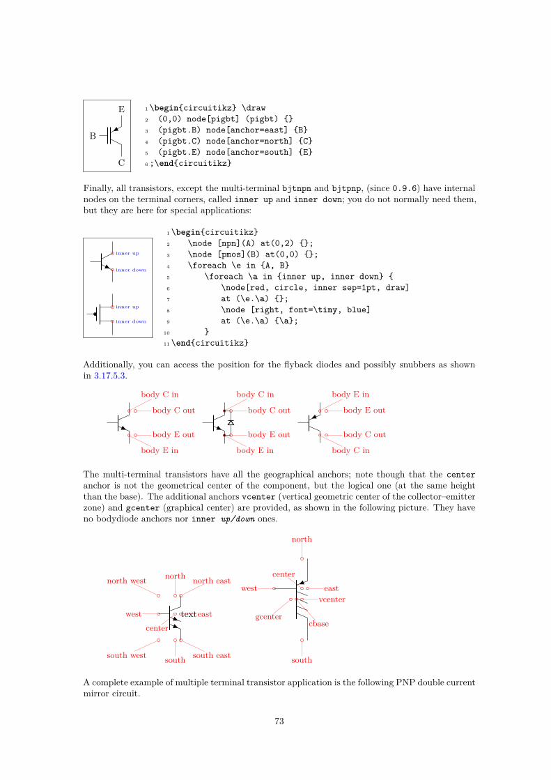
B
C
E 1\begincircuitikz \draw2 (0,0) node[pigbt] (pigbt) 3 (pigbt.B) node[anchor=east] B4 (pigbt.C) node[anchor=north] C5 (pigbt.E) node[anchor=south] E6;\endcircuitikz
Finally, all transistors, except the multi-terminal bjtnpn and bjtpnp, (since 0.9.6) have internalnodes on the terminal corners, called inner up and inner down; you do not normally need them,but they are here for special applications:
inner up
inner down
inner up
inner down
1\begincircuitikz2 \node [npn](A) at(0,2) ;3 \node [pmos](B) at(0,0) ;4 \foreach \e in A, B5 \foreach \a in inner up, inner down 6 \node[red, circle, inner sep=1pt, draw]7 at (\e.\a) ;8 \node [right, font=\tiny, blue]9 at (\e.\a) \a;
10 11\endcircuitikz
Additionally, you can access the position for the flyback diodes and possibly snubbers as shownin 3.17.5.3.
body C in
body E in
body C out
body E out
body C in
body E in
body C out
body E out
body C in
body E in
body C out
body E out
The multi-terminal transistors have all the geographical anchors; note though that the centeranchor is not the geometrical center of the component, but the logical one (at the same heightthan the base). The additional anchors vcenter (vertical geometric center of the collector–emitterzone) and gcenter (graphical center) are provided, as shown in the following picture. They haveno bodydiode anchors nor inner up/down ones.
text
north north east
east
south eastsouthsouth west
west
north west
center
north
east
south
westcenter
vcenter
gcentercbase
A complete example of multiple terminal transistor application is the following PNP double currentmirror circuit.
73

Q1 Q2
R0
I0
I0 I0
1 \begincircuitikz2 \ctikzsettransistors/arrow pos=end3 \draw (0,0) node[bjtpnp, xscale=-1](Q1)%4 \scalebox-1[1]Q1;5 \draw (Q1.B) node[bjtpnp, anchor=B, collectors=2]6 (Q2)Q2 (Q1.B) node[circ];7 \draw (Q1.E) node[circ] node[vcc] (Q2.E)8 node[vcc] (Q1.E) -| (Q1.B);9 \draw (Q1.C) to[R, l_=$R_0$, f=$I_0$] ++(0,-3.5)
10 node[ground](GND);11 \draw (Q2.C) -- ++(0,-0.5) coordinate(a);12 \draw (Q2.C1) -- ++(1,0) coordinate(b) -- (b|-a);13 \draw (a) ++(0,-0.1) node[flowarrow, rotate=-90,14 anchor=west]\rotatebox90$I_0$;15 \draw (b|-a) ++(0,-0.1) node[flowarrow, rotate=-90,16 anchor=west]\rotatebox90$I_0$;17 \path (b) ++(0.5,0); % bounding box adjust18 \endcircuitikz
Here is one composite example (please notice that the xscale=-1 style would also reflect the labelof the transistors, so here a new node is added and its text is used, instead of that of pnp1):
Q2Q1
Q3 Q4
1 % \begincircuitikz [legacy transistors label]\draw2 \begincircuitikz []\draw3 (0,0) node[pnp] (pnp2) Q24 (pnp2.B) node[pnp, xscale=-1, anchor=B] (pnp1) 5 (pnp1) node[left, inner sep=0pt] Q16 (pnp1.C) node[npn, anchor=C] (npn1) Q37 (pnp2.C) node[npn, xscale=-1, anchor=C] (npn2)8 \scalebox-1[1]Q49 (pnp1.E) -- (pnp2.E) (npn1.E) -- (npn2.E)
10 (pnp1.B) node[circ] |- (pnp2.C) node[circ] 11;\endcircuitikz
Notice that the text labels of transistors are somewhat buggy. It is better to se explicit anchorsto set transistor’s names.Similarly, transistors like other components can be reflected vertically:
BulkG
D
S
1\begincircuitikz \draw2 (0,0) node[pigfete, yscale=-1] (pigfete) 3 (pigfete.bulk) node[anchor=west] Bulk4 (pigfete.G) node[anchor=east] G5 (pigfete.D) node[anchor=south] D6 (pigfete.S) node[anchor=north] S7;\endcircuitikz
3.17.8 Transistor paths
For syntactical convenience standard transistors (not multi-terminal ones) can be placed using thenormal path notation used for bipoles. The transitor type can be specified by simply adding a “T”(for transistor) in front of the node name of the transistor. It will be placed with the base/gateorthogonal to the direction of the path:
74

1
2 3 1\begincircuitikz \draw2 (0,0) node[njfet] 13 (-1,2) to[Tnjfet=2] (1,2)4 to[Tnjfet=3, mirror] (3,2);5;\endcircuitikz
Access to the gate and/or base nodes can be gained by naming the transistors with the n or namepath style:
p1
n1
n2
p2 1\begincircuitikz \draw[yscale=1.1, xscale=.8]2 (2,4.5) -- (0,4.5) to[Tpmos=p1, n=p1] (0,3)3 to[Tnmos=n1, n=n1] (0,1.5)4 to[Tnmos=n2, n=n2] (0,0) node[ground] 5 (2,4.5) to[Tpmos=p2,n=p2] (2,3) to[short, -*]
(0,3)6 (p1.G) -- (n1.G) to[short, *-o] ($(n1.G)+(3,0)$)7 (n2.G) ++(2,0) node[circ] -| (p2.G)8 (n2.G) to[short, -o] ($(n2.G)+(3,0)$)9 (0,3) to[short, -o] (-1,3)
10;\endcircuitikz
Transistor paths have the possibility to use the poles syntax (see section 5.1) but they have novoltage, current, flow, annotation options. Also, the positioning of the labels is very simple and isnot foolproof for all rotations; if you need to control them more please name the node and positionthem by hand, or use the more natural node style for transistors.The name property is available also for bipoles; this is useful mostly for triac, potentiometer andthyristor (see 3.7.1).
3.18 Electronic Tubes
Electronic tubes, also known as vacuum tubes, control current flow between electrodes. Theycome in many different flavours. Contributed by J. op den Brouw ([email protected]).
anode
cathode
Tube Diode, type: node, fillable (node[diodetube]). Class:tubes.
75

anode
cathode
control Triode, type: node, fillable (node[triode]). Class: tubes.
anode
cathode
control
screenTetrode, type: node, fillable (node[tetrode]). Class: tubes.
anode
cathode
controlscreen
suppressorPentode, type: node, fillable (node[pentode]). Class:tubes.
Some pentodes have the suppressor grid internally connected to the control grid, which saves a pin on thetube’s housing.
anode
cathode
controlscreen
Pentode with suppressor grid connected to cathode, type:node, fillable (node[pentode suppressor to cathode]).Class: tubes.
Note that the diodetube is used as component name to avoid clashes with the semiconductor diode.Normally, the filament is not drawn. If you want a filament, put the filament option in the nodedescription:
anode
filament 1 filament 2
Tube Diode, type: node, fillable(node[diodetube,filament]). Class: tubes.
76

Sometimes, you don’t want the cathode to be drawn (but you do want the filament). Use the nocathodeoption in the node description:
anode
Tube Diode, type: node, fillable(node[diodetube,filament,nocathode]). Class: tubes.
If you want a full cathode to be drawn, use the fullcathode option in the node description. You can thenuse the anchors cathode 1 and cathode 2.
anode
cathode 1 cathode 2
Tube Diode, type: node, fillable(node[diodetube,fullcathode]). Class: tubes.
3.18.1 Tubes customization
The tubes can be scaled using the key tubes/scale, default 1.0. In addition, they are fully configurable,and the attributes are described below:Key Default value Descriptiontubes/scale 1 scale factortubes/width 1 relative widthtubes/height 1.4 relative heighttubes/tube radius 0.40 radius of tube circletubes/anode distance 0.40 distance from centertubes/anode width 0.40 width of an anode/platetubes/grid protrusion 0.25 distance from centertubes/grid dashes 5 number of grid dashestubes/grid separation 0.2 separation between gridstubes/grid shift 0.0 y shift of grids from centertubes/cathode distance 0.40 distance from gridtubes/cathode width 0.40 width of a cathodetubes/cathode corners 0.06 corners of the cathode wiretubes/cathode right extend 0.075 extension at the right sidetubes/filament distance 0.1 distance from cathodetubes/filament angle 15 angle from the centerpoint
Conventionally, the model of the tube is indicated at the east anchor:
77

12AX7
1\ctikzsettubes/width=1.42\ctikzsettubes/height=13
4\begincircuitikz5\draw (0,0) node[triode] (Tri) ;6\draw (Tri.east) node[right] 12AX7;7\endcircuitikz
Example triode amplifier:
1\begincircuitikz2\draw (0,0) node (start) 3 to[sV=$V_i$] ++(0,2+\ctikzvaloftubes/height)4 to[C=$C_i$] ++(2,0) node (Rg) 5 to[R=$R_g$] (Rg |- start)6(Rg) to[short,*-] ++(1,0)7 node[triode,anchor=control] (Tri) ++(2,0)8(Tri.cathode) to[R=$R_c$,-*] (Tri.cathode |- start)9(Tri.anode) to [R=$R_a$] ++(0,2)
10 to [short] ++(3.5,0) node(Vatop) 11 to [V<=$V_a$] (Vatop |- start)12 to [short] (start)13(Tri.anode) ++(0,0.2) to[C=$C_o$,*-o] ++(2,0)14(Tri.cathode) ++(0,-0.2) to[short,*-] ++(1.5,0) node(Cctop) 15 to[C=$C_c$,-*] (start -| Cctop)16;17\draw[red,thin,dashed] (Tri.north west) rectangle (Tri.south east);18\draw (Tri.east) node[right] 12AX7;19\endcircuitikz
Vi
Ci
Rg
Rc
Ra
Va
Co
Cc
12AX7
The magnetron shape will also scale with tubes/scale.
78

anode
cathode1 cathode2
left right
top
Magnetron, type: node, fillable (node[magnetron]). Class:tubes.
HV1 2
RFout
1\begincircuitikz2\draw (0,-2)node[rground](gnd) to[voltage
source,v<=HV]++(0,3)--++(1,0)to[V,n=DC]++(2,0);
3\draw (2,-1) node[magnetron,scale=1](magn);
4\draw (DC.left)++(-0.2,0)to [short,*-]++(0,-1) to [short] (magn.cathode1);
5\draw (DC.right)++(0.2,0)to [short,*-]++(0,-1) to [short] (magn.cathode2);
6\draw (magn.anode) to [short] (magn.anode|-gnd) node[rground];
7\draw (magn.cathode1)node[above]$1$;8\draw (magn.cathode2)node[above]$2$;9\draw[->](magn.east) --++(1,0)node[right]$
RF_out$;10\endcircuitikz
3.19 RF componentsFor the RF components, similarly to the grounds and supply rails, the center anchor is put on theconnecting point of the symbol, so that you can use them directly in a path specification.Notes that in the transmission and receiving antennas, the “waves” are outside the geographical anchors.
A
top
bottomleft
right
center
Bare Antenna, type: node, fillable (node[bareantenna]A).Class: RF.
Tx
top
center
wavesBare TX Antenna, type: node, fillable(node[bareTXantenna]Tx). Class: RF.
Rx
top
center
wavesBare RX Antenna, type: node, fillable(node[bareRXantenna]Rx). Class: RF.
north north east
east
south eastsouthsouth west
west
north west
left
top
right
bottom
Waves, type: node (node[waves]). Class: RF.
79

left right
center
mstline: Microstrip transmission line14, type: path-style,fillable, nodename: mstlineshape. Class: RF.
textleft right
center
Microstrip linear stub, type: node, fillable(node[mslstub]text). Class: RF.
Tleft right
center
Microstrip port, type: node, fillable (node[msport]T). Class:RF.
left right
center
Microstrip radial stub, type: node, fillable (node[msrstub]).Class: RF.
center
Legacy antenna (with tails), type: node (node[antenna]).Class: RF.
Legacy receiving antenna (with tails), type: node(node[rxantenna]). Class: RF.
Legacy transmitting antenna (with tails), type: node(node[txantenna]). Class: RF.
Transmission line stub, type: node, fillable(node[tlinestub]). Class: RF.
TL: Transmission line, type: path-style, fillable,nodename: tlineshape.Aliases: transmission line, tline.Class: RF.
match, type: node (node[match]). Class: RF.
3.19.1 RF elements customization
The RF elements can be scaled using the key RF/scale, default 1.0.14This four components were suggested by @tcpluess on GitHub
80

3.19.2 Microstrip customization
The microstrip linear components’ (mstline, mslstub, msport) heights can be changed by setting theparameter bipoles/mstline/height (for the three of them, default 0.3). The widths are specified inbipoles/mstline/width for the first two and by monopoles/msport/width for the port (defaults: 1.2,0.5).For the length parameter of the transmission line there is a shortcut in the form of the direct parametermstlinelen.
longer stubshort
1\begincircuitikz2 \draw (0,0) node[msport, right, xscale=-1]3 to[mstline, -o] ++(3,0) coordinate(there)4 to[mstline, mstlinelen=2, l=longer, o-*] ++(4,0)5 coordinate(here) -- ++(0.5,0) node[mslstub, fill=yellow]stub6 (here) -- ++(0,0.5) node[mslstub, rotate=90, mstlinelen=0.5]short;7 \draw (there) to[short, o-] ++(0, 0.5) node[msrstub];8 \draw (here) -- ++(0, -0.5) node[msrstub, yscale=-1];9\endcircuitikz
3.20 Electro-Mechanical Devices
The internal part of the motor and generator are, by default, filled white (to avoid compatibility problemswith older versions of the package).
M
bottom
left right
top
45Motor, type: node, fillable (node[elmech]M). Class:electromechanicals.
Gblock down right
block north eastGenerator, type: node, fillable (node[elmech]G). Class:electromechanicals.
3.20.1 Electro-Mechanical Devices anchors
Apart from the standard geographical anchors, elmech has the border anchors (situated on the inner circle)and the following anchors on the “block”:
81

A
block north east
block south eastblock south west
block north west150
180210
60-60 B
block up right
block down rightblock down left
block up leftnorth
south
eastwest
Mω
1\begincircuitikz2\draw (2,0) node[elmech](motor)M;3\draw (motor.north) |-(0,2) to [R] ++(0,-2) to[
dcvsource]++(0,-2) -| (motor.bottom);4\draw[thick,->>](motor.right)--++(1,0)node[midway,
above]$\omega$;5\endcircuitikz
ω
1\begincircuitikz2\draw (2,0) node[elmech](motor);3\draw (motor.north) |-(0,2) to [R] ++(0,-2) to[
dcvsource]++(0,-2) -| (motor.bottom);4\draw[thick,->>](motor.center)--++(1.5,0)node[midway,
above]$\omega$;5\endcircuitikz
The symbols can also be used along a path, using the transistor-path-syntax(T in front of the shape name,see section 3.17.8). Don’t forget to use parameter n to name the node and get access to the anchors:
M
M
Gω
1\begincircuitikz2\draw (0,0) to [Telmech=M,n=motor] ++(0,-3) to [
Telmech=M] ++(3,0) to [Telmech=G,n=generator]++(0,3) to [R] (0,0);
3\draw[thick,->>](motor.left)--(generator.left)node[midway,above]$\omega$;
4\endcircuitikz
3.21 Double bipoles (transformers)
Transformers automatically use the inductor shape currently selected. These are the three possibilities:
A1
A2
B1
B2
inner dot A1
inner dot A2
inner dot B1
inner dot B2
Transformer (cute inductor), type: node(node[transformer]). Class: inductors.
82

outer dot A1
outer dot A2
outer dot B1
outer dot B2
Transformer (american inductor), type: node(node[transformer]). Class: inductors.
Transformer (european inductor), type: node(node[transformer]). Class: inductors.
Gyrator, type: node, fillable (node[gyrator]). Class:inductors.
Transformers with core are also available:
Transformer core (cute inductor), type: node(node[transformer core]). Class: inductors.
Transformer core (american inductor), type: node(node[transformer core]). Class: inductors.
Transformer core (european inductor), type: node(node[transformer core]). Class: inductors.
3.21.1 Double dipoles anchors
All the double bipoles/quadrupoles have the four anchors, two for each port. The first port, to the left, isport A, having the anchors A1 (up) and A2 (down); same for port B.They also expose the base anchor, for labelling, and anchors for setting dots or signs to specify polarity.The set of anchors, to which the standard “geographical” north, north east, etc. is here:
inner dot A1
inner dot A2
inner dot B1
inner dot B2
outer dot A1
outer dot A2
outer dot B1
outer dot B2
A1
A2
B1
B2
base
83

Also, the standard “geographical” north, north east, etc. are defined. A couple of examples follow:
A1
A2
B1
B2
K
1\begincircuitikz \draw2 (0,0) node[transformer] (T) 3 (T.A1) node[anchor=east] A14 (T.A2) node[anchor=east] A25 (T.B1) node[anchor=west] B16 (T.B2) node[anchor=west] B27 (T.base) nodeK8 (T.inner dot A1) node[circ]9 (T.inner dot B2) node[circ]
10;\endcircuitikz
A1
A2
B1
B2
K1\begincircuitikz \draw2 (0,0) node[gyrator] (G) 3 (G.A1) node[anchor=east] A14 (G.A2) node[anchor=east] A25 (G.B1) node[anchor=west] B16 (G.B2) node[anchor=west] B27 (G.base) nodeK8;\endcircuitikz
Moreover, you can access the two internal coils (inductances); if your transformer node is called T, theyare named T-L1 and T-L2. Notice that the two inductors are rotated (by -90 degrees the first, +90 degreesthe second) so you have to be careful with the anchors. Also, the midtap anchor of the inductors can beon the external or internal side depending on the numbers of coils. Finally, the anchors L1.a and L1.bare marking the start and end of the coils.
T-L1.midtap
T-L1.south west
T-L1.south east
T-L2.south
T-L2.south west
T-L2.south east
T-L1.a
T-L1.b
T-L2.midtap
T-L2.south west
T-L2.south east
inductors/coils=5T-L2.a
T-L2.b
T-L2.midtap
T-L2.south west
T-L2.south east
inductors/coils=6
1 \begincircuitikz2 \draw (0,0) node[ground](GND) to [sV] ++(0,2) -- ++(1,0)3 node[transformer, circuitikz/inductors/coils=6,4 anchor=A1](T);5 \draw (T.A2) to[short, -*] (T.A2-|GND);6 \draw (T-L2.midtap) to[short, *-o] (T.B1 |- T-L2.midtap);7 \node [ocirc] at (T.B1); \node [ocirc] at (T.B2);8 \endcircuitikz
3.21.2 Double dipoles customization
Transformers are in the inductors class (also the gyrator…), so they scale with the key inductors/scale.You can change the aspect of a quadpole using the corresponding parameters quadpoles/*/width andquadpoles/*/heigth (substitute the star for transformer, transformer core or gyrator; default valueis 1.5 for all). You have to be careful to not choose value that overlaps the components!
84

K 1\begincircuitikz2\ctikzsetquadpoles/transformer/width=1,3 quadpoles/transformer/height=24 \draw (0,0) node[transformer] (T) 5 (T.base) nodeK6 (T.inner dot A1) node[circ]7 (T.inner dot B2) node[circ];8\endcircuitikz
Transformers also inherits the inductors/scale (see 3.6.5) and similar parameters. It’s your responsibilityto set the aforementioned parameters if you change the scale or width of inductors.Transformers core line distance is specified by the parameter quadpoles/transformer core/core width(default 0.05) and the thickness of the lines follows the choke one; in other words, you can set it changingbipoles/cutechoke/cthick.Another very useful parameter is quadpoles/*/inner (default 0.4) that determine which part of thecomponent is the “vertical” one. So, setting that parameter to 1 will eliminate the horizontal part of thecomponent (obviously, to maintain the general aspect ratio you need to change the width also):
A1
A2
B1
B2
K
T
1\begincircuitikz2\draw (0,0) node[transformer] (T) 3 (T.A1) node[anchor=east] A14 (T.A2) node[anchor=east] A25 (T.B1) node[anchor=west] B16 (T.B2) node[anchor=west] B27 (T.base) nodeK ;8\ctikzsetquadpoles/transformer/inner=1, quadpoles/
transformer/width=0.69\draw (0,-3) node[transformer] (P)
10 (P.base) nodeT11 (P.inner dot A2) node[ocirc]12 (P.inner dot B2) node[ocirc];13\endcircuitikz
This can be useful if you want to put seamlessly something in series with either side of the component;for simplicity, you have a style setting quadpoles style to toggle between the standard shape of doublebipoles (called inward, default) and the one without horizontal leads (called inline):
⊕
+
1\begincircuitikz2\ctikzsetinductor=cute, quadpoles style=inline3\draw4 (0,0) to[R] ++(0,-2)5 node[transformer, anchor=A1](T)6 (T.A2) node[ground](GND)7 (T.inner dot A1) node[font=\small\boldmath]$\oplus$8 (T.inner dot B2) node[]$+$9 (T.B1) node[above, ocirc]
10 (T.B2) -- (GND);11\endcircuitikz
85

3.21.3 Styling transformer’s coils independently
Since 0.9.6, you can tweak the style of each of the coils of the transformers by changing the value ofthe two styles transformer L1 and transformer L2; the default for both are , that means inherit theinductors style in force.
1 \begincircuitikz[american]2 \beginscope3 \ctikzsettransformer L1/.style=inductors/coils=1, inductors/width=0.24 \draw (0,0) node[transformer core](T1);5 \endscope6 \draw (3,0) node[transformer](T2);7 \ctikzsetcute inductors, quadpoles style=inline8 \ctikzsettransformer L1/.style=inductors/coils=2, inductors/width=0.29 \draw (6,0) node[transformer core](T3);
10 \ctikzsettransformer L1/.style=american inductors, inductors/coils=1, inductors/width=0.2
11 \ctikzsettransformer L2/.style=inductors/coils=7, inductors/width=1.012 \draw (9,0) node[transformer ](T4);13 \foreach \t in T1, T2, T3, T4 14 \foreach \l in L1, L2 15 \foreach \a/\c in a/blue, b/red16 \node [circle, fill=\c, inner sep=1pt] at (\t-\l.\a) ;17 18 19 \endcircuitikz
Caveat: the size of the transformer is independent from the styles for L1 and L2, so they follow whateverthe parameters for the inductances were before applying them. In other words, the size of the transformercould result too small if you are not careful.
1 \begincircuitikz2 \ctikzsettransformer L1/.style=inductors/width=1.8,
inductors/coils=133 % too small!4 \draw (0,0) node[transformer core](T1);5 % adjust it6 \ctikzsetquadpoles/transformer core/height=2.47 \draw (2.5,0) node[transformer core](T1);8 \endcircuitikz
You can obviously define a style for a “non-standard” transformer. For example, you can have a currenttransformer15 defined like this:
15Suggested by Alex Pacini on GitHub
86

1 \begincircuitikz[2 TA core/.style=transformer core,3 % at tikz level, you have to use circuitikz/ explicitly4 circuitikz/quadpoles style=inline,5 circuitikz/transformer L1/.style=6 american inductors, inductors/coils=1,7 inductors/width=0.3,8 ]9 \draw (0,0) node[TA core](T1);
10 % changes are local11 \draw (0,-3) node[transformer];12 \endcircuitikz
Remember that the default pgfkeys directory is /tikz for nodes and for the options of the environment,so you have to use the full path (with circuitikz/) there.
3.22 Amplifiers
−
++
-out
up
down
Operational amplifier, type: node, fillable (node[op amp]).Class: amplifiers.
−
+
▷∞Operational amplifier compliant to DIN/EN 60617 standard,type: node, fillable (node[en amp]). Class: amplifiers.
−
+−+
out +
out -
Fully differential operational amplifier16, type: node, fillable(node[fd op amp]). Class: amplifiers.
−
+
transconductance amplifier, type: node, fillable (node[gmamp]). Class: amplifiers.
−
+
up
down
refv up
refv down
plain instrumentation amplifier, type: node, fillable(node[inst amp]). Class: amplifiers.
16Contributed by Kristofer M. Monisit.
87
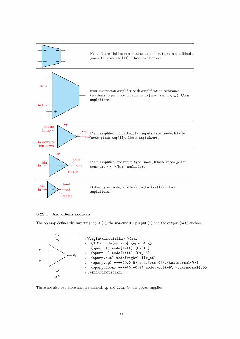
−
+ −
+Fully differential instrumentation amplifier, type: node, fillable(node[fd inst amp]). Class: amplifiers.
−
+
ra+
ra-instrumentation amplifier with amplification resistanceterminals, type: node, fillable (node[inst amp ra]). Class:amplifiers.
in up
in down
up
out
bin up
bin down
bout Plain amplifier, unmarked, two inputs, type: node, fillable(node[plain amp]). Class: amplifiers.
in out
up
center
bin bout Plain amplifier, one input, type: node, fillable (node[plainmono amp]). Class: amplifiers.
in out
center
bin boutBuffer, type: node, fillable (node[buffer]). Class:amplifiers.
3.22.1 Amplifiers anchors
The op amp defines the inverting input (-), the non-inverting input (+) and the output (out) anchors:
−
+v+
v−
vo
5V
-5V
1\begincircuitikz \draw2 (0,0) node[op amp] (opamp) 3 (opamp.+) node[left] $v_+$4 (opamp.-) node[left] $v_-$5 (opamp.out) node[right] $v_o$6 (opamp.up) --++(0,0.5) node[vcc]5\,\textnormalV7 (opamp.down) --++(0,-0.5) node[vee]-5\,\textnormalV8;\endcircuitikz
There are also two more anchors defined, up and down, for the power supplies:
88

−
+v+
v−
vo
12V
1\begincircuitikz \draw2 (0,0) node[op amp] (opamp) 3 (opamp.+) node[left] $v_+$4 (opamp.-) node[left] $v_-$5 (opamp.out) node[right] $v_o$6 (opamp.down) node[ground] 7 (opamp.up) ++ (0,.5) node[above] \SI12\volt8 -- (opamp.up)9;\endcircuitikz
The fully differential op amp defines two outputs:
−
+−+
v+
v− out +
out -
1\begincircuitikz \draw2 (0,0) node[fd op amp] (opamp) 3 (opamp.+) node[left] $v_+$4 (opamp.-) node[left] $v_-$5 (opamp.out +) node[right] out +6 (opamp.out -) node[right] out -7 (opamp.down) node[ground] 8;\endcircuitikz
The instrumentation amplifier inst amp defines also references (normally you use the down, unless you areflipping the component):
−
+v+
v−
out
1\begincircuitikz \draw2 (0,0) node[inst amp] (opamp) 3 (opamp.+) node[left] $v_+$4 (opamp.-) node[left] $v_-$5 (opamp.out) node[right] out6 (opamp.up) node[vcc]7 (opamp.down) node[vee] 8 (opamp.refv down) node[ground]9 (opamp.refv up) to[short, -o] ++(0,0.3)
10;\endcircuitikz
The fully diffential instrumentation amplifier inst amp defines two outputs:
−
+ −
+
v+
v− out +
out -
1\begincircuitikz \draw2 (0,0) node[fd inst amp] (opamp) 3 (opamp.+) node[left] $v_+$4 (opamp.-) node[left] $v_-$5 (opamp.out +) node[right] out +6 (opamp.out -) node[right] out -7 (opamp.up) node[vcc]8 (opamp.down) node[vee] 9 (opamp.refv down) node[ground]
10 (opamp.refv up) to[short, -o] ++(0,0.3)11;\endcircuitikz
The instrumentation amplifier with resistance terminals (inst amp ra) defines also terminals to add anamplification resistor:
89

−
+v+
v−
out
1\begincircuitikz \draw2 (0,0) node[inst amp ra] (opamp) 3 (opamp.+) node[left] $v_+$4 (opamp.-) node[left] $v_-$5 (opamp.out) node[right] out6 (opamp.up) node[vcc]7 (opamp.down) node[vee] 8 (opamp.refv down) node[ground]9 (opamp.refv up) to[short, -o] ++(0,0.3)
10 (opamp.ra-) to[R] (opamp.ra+)11;\endcircuitikz
Amplifiers have also “border” anchors (just add b, without space, to the anchor, like b+ or bin up and soon). These can be useful to add “internal components” or to modify the component. Also the leftedgeanchors (on the border midway between input) is available.
−
+
IA1
A
1 \begincircuitikz[]2 \draw (0,2.2) node[op amp](OA)IA1;3 \node[oosourceshape, rotate=90, scale=0.5]4 at (OA.leftedge) ;5 \draw (0,0) node[plain amp](A)$A$;6 \draw [color=red] (A.bin up) -- ++(0.2,0)7 coordinate (tmp)8 to[R, resistors/scale=0.5]9 (tmp|-A.bin down) -- (A.bin down);
10 \endcircuitikz
3.22.2 Amplifiers customization
You can scale the amplifiers using the key amplifiers/scale and setting it to something different from1.0. The font used for symbols will not scale, so it’s your responsibility to change it if the need arises.All these amplifier have the possibility to flip input and output (if needed) polarity. You can changepolarity of the input with the noinv input down (default) or noinv input up key; and the output withnoinv output up (default) or noinv output down key:
+
− +
−v+
v− out +
out -
1\begincircuitikz \draw2 (0,0) node[fd inst amp,3 noinv input up,4 noinv output down] (opamp) 5 (opamp.+) node[left] $v_+$6 (opamp.-) node[left] $v_-$7 (opamp.out +) node[right] out +8 (opamp.out -) node[right] out -9 (opamp.up) node[vcc]
10 (opamp.down) node[vee] 11 (opamp.refv down) node[ground]12 (opamp.refv up) to[short, -o] ++(0,0.3)13;\endcircuitikz
When you use the noinv input/output ... keys the anchors (+, -, out +, out -) will change with theeffective position of the terminals. You have also the anchors in up, in down, out up, out down that willnot change with the positive or negative sign.You can change the symbols “+” or “−” appearing in the amplifiers if you want, both globally and oncomponent-by-component basis. The plus and minus symbols can be changed with \ctikzset of the keys
90
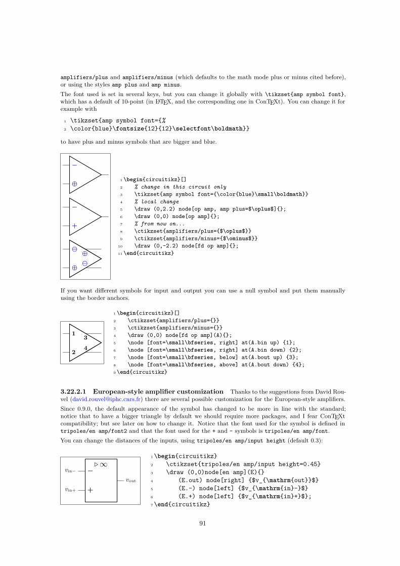
amplifiers/plus and amplifiers/minus (which defaults to the math mode plus or minus cited before),or using the styles amp plus and amp minus.The font used is set in several keys, but you can change it globally with \tikzsetamp symbol font,which has a default of 10-point (in LATEX, and the corresponding one in ConTEXt). You can change it forexample with
1 \tikzsetamp symbol font=%2 \colorblue\fontsize1212\selectfont\boldmath
to have plus and minus symbols that are bigger and blue.
−
⊕
−
+
⊖
⊕⊖⊕
1 \begincircuitikz[]2 % change in this circuit only3 \tikzsetamp symbol font=\colorblue\small\boldmath4 % local change5 \draw (0,2.2) node[op amp, amp plus=$\oplus$];6 \draw (0,0) node[op amp];7 % from now on...8 \ctikzsetamplifiers/plus=$\oplus$9 \ctikzsetamplifiers/minus=$\ominus$
10 \draw (0,-2.2) node[fd op amp];11 \endcircuitikz
If you want different symbols for input and output you can use a null symbol and put them manuallyusing the border anchors.
1
2
34
1 \begincircuitikz[]2 \ctikzsetamplifiers/plus=3 \ctikzsetamplifiers/minus=4 \draw (0,0) node[fd op amp](A);5 \node [font=\small\bfseries, right] at(A.bin up) 1;6 \node [font=\small\bfseries, right] at(A.bin down) 2;7 \node [font=\small\bfseries, below] at(A.bout up) 3;8 \node [font=\small\bfseries, above] at(A.bout down) 4;9 \endcircuitikz
3.22.2.1 European-style amplifier customization Thanks to the suggestions from David Rou-vel ([email protected]) there are several possible customization for the European-style amplifiers.Since 0.9.0, the default appearance of the symbol has changed to be more in line with the standard;notice that to have a bigger triangle by default we should require more packages, and I fear ConTEXtcompatibility; but see later on how to change it. Notice that the font used for the symbol is defined intripoles/en amp/font2 and that the font used for the + and - symbols is tripoles/en amp/font.You can change the distances of the inputs, using tripoles/en amp/input height (default 0.3):
−
+
▷∞
vout
vin−
vin+
1\begincircuitikz2 \ctikzsettripoles/en amp/input height=0.453 \draw (0,0)node[en amp](E)4 (E.out) node[right] $v_\mathrmout$5 (E.-) node[left] $v_\mathrmin-$6 (E.+) node[left] $v_\mathrmin+$;7\endcircuitikz
91

and of course the key noinv input up is fully functional:
+
−
▷∞
vout
vin−
vin+
1\begincircuitikz2 \ctikzsettripoles/en amp/input height=0.453 \draw (0,0)node[en amp, noinv input up](E)4 (E.out) node[right] $v_\mathrmout$5 (E.-) node[left] $v_\mathrmin-$6 (E.+) node[left] $v_\mathrmin+$;7\endcircuitikz
To flip the amplifier in the horizontal direction, you can use xscale=-1 as usual:
+
−
▷∞
vout
vin−
vin+
1\begincircuitikz2 \ctikzsettripoles/en amp/input height=0.453 \draw (0,0)node[en amp, xscale=-1, noinv input up
](E)4 (E.out) node[left] $v_\mathrmout$5 (E.-) node[right] $v_\mathrmin-$6 (E.+) node[right] $v_\mathrmin+$;7\endcircuitikz
Notice that the label is fully mirrored, so check below for the generic way to change this.You can use the new key en amp text A to change the infinity symbol with an A:
−
+
▷A
vout
vin−
vin+
1\begincircuitikz2 \draw (0,0)node[en amp, en amp text A](E)3 (E.out) node[right] $v_\mathrmout$4 (E.-) node[left] $v_\mathrmin-$5 (E.+) node[left] $v_\mathrmin+$ ;6\endcircuitikz
And if you want, you can completely change the text using the key en amp text=, which by default is$\mathstrut\triangleright\,\infty$:
−
+
▷ 200
vout
vin−
vin+
1\begincircuitikz2 \draw (0,0)node[en amp, en amp text=%3 $\triangleright$ \small 200](E)4 (E.out) node[right] $v_\mathrmout$5 (E.-) node[left] $v_\mathrmin-$6 (E.+) node[left] $v_\mathrmin+$ ;7\endcircuitikz
Notice two things here: the first, that \triangleright is enclosed in braces to remove the default spacingit has as a binary operator, and that en amp text A is simply a shortcut for
1 en amp text=$\mathstrut\triangleright\,\mathrmA$
To combine flipping with a generic label you just do:
−
+
▷A
vout
vin−
vin+
1\begincircuitikz2 \draw (0,0)node[en amp, xscale=-1, en amp text A](
E)3 (E.out) node[left] $v_\mathrmout$4 (E.-) node[right] $v_\mathrmin-$5 (E.+) node[right] $v_\mathrmin+$ ;6\endcircuitikz
92

But notice that the “A” is also flipped by the xscale parameter. So the solution in this case is to usescalebox, like this:
−
+
▷200
vout
vin−
vin+
1\begincircuitikz2 \draw (0,0)node[en amp, xscale=-1, en amp text=%3 $\triangleright$ \scalebox-1[1]\small 200](
E)4 (E.out) node[left] $v_\mathrmout$5 (E.-) node[right] $v_\mathrmin-$6 (E.+) node[right] $v_\mathrmin+$ ;7\endcircuitikz
3.22.3 Designing your own amplifier
If you need a different kind of amplifier, you can use the muxdemux (see section 3.26) shape for definingone that suits your needs (you need version 1.0.0 for this to work).
TDA1 TDA2
1 \tikzsettdax/.style=muxdemux,2 muxdemux def=NL=2, Lh=3, NR=1, Rh=0,3 NB=4, NT=5, font=\scriptsize\ttfamily4 \begincircuitikz5 \draw (0,0) node[tdax](A)TDA1;6 \draw (2.5,0) node[tdax,7 muxdemux def=Rh=0.5]TDA2;8 \endcircuitikz
3.23 Switches and buttonsSwitches and button come in to-style (the simple ones and the pushbuttons), and as nodes.The switches can be scaled with the key switches/scale (default 1.0). Notice that scaling the switcheswill not scale the poles, which are controlled with their own parameters (see section 3.15).
3.23.1 Traditional switches
These are all of the to-style type:
switch: Switch, type: path-style, nodename:cspstshape.Aliases: spst. Class: switches.
closing switch: Closing switch, type: path-style,nodename: cspstshape.Aliases: cspst. Class: switches.
opening switch: Opening switch, type: path-style,nodename: ospstshape.Aliases: ospst. Class: switches.
normal open switch: Normally open switch, type:path-style, nodename: nosshape.Aliases: nos. Class:switches.
normal closed switch: Normally closed switch, type:path-style, nodename: ncsshape.Aliases: ncs. Class:switches.
push button: Normally open push button, type:path-style, nodename: pushbuttonshape.Aliases: normallyopen push button, nopb. Class: switches.
93

normally closed push button: Normally closed push button,type: path-style, nodename: ncpushbuttonshape.Aliases:ncpb. Class: switches.
toggle switch: Toggle switch, type: path-style,nodename: toggleswitchshape. Class: default.
reed: Reed switch, type: path-style, fillable, nodename:reedshape. Class: switches.
while this is a node-style component:
inout 1
out 2spdt, type: node (node[spdt]). Class: switches.
inout 1
out 2
1\begincircuitikz \draw2 (0,0) node[spdt] (Sw) 3 (Sw.in) node[left] in4 (Sw.out 1) node[right] out 15 (Sw.out 2) node[right] out 26;\endcircuitikz
1\begincircuitikz \draw2 (0,0) to[C] (1,0) to[toggle switch , n=Sw] (2.5,0)3 -- (2.5,-1) to[battery1] (1.5,-1) to[R] (0,-1) -| (0,0)4 (Sw.out 2) -| (2.5, 1) to[R] (0,1) -- (0,0)5;\endcircuitikz
3.23.2 Cute switches
These switches have been introduced after version 0.9.0, and they come in also in to-style and in node-style,but they are size-matched so that they can be used together in a seamless way.The path element (to-style) are:
mid
in out
cute closed switch: Cute closed switch, type: path-style,nodename: cuteclosedswitchshape.Aliases: ccsw. Class:switches.
out
B-out.s
cute open switch: Cute open switch, type: path-style,name=B, nodename: cuteopenswitchshape.Aliases: cosw.Class: switches.
cute closing switch: Cute closing switch, type:path-style, nodename: cuteclosingswitchshape.Aliases:ccgsw. Class: switches.
cute opening switch: Cute opening switch, type:path-style, nodename: cuteopeningswitchshape.Aliases:cogsw. Class: switches.
while the node-style components are the single-pole, double-throw (spdt) ones:
94

inout 1
out 2
mid Cute spdt up, type: node (node[cute spdt up]). Class:switches.
Cute spdt mid, type: node (node[cute spdt mid]). Class:switches.
midCute spdt down, type: node (node[cute spdt down]).Class: switches.
Cute spdt up with arrow, type: node (node[cute spdt uparrow]). Class: switches.
Cute spdt mid with arrow, type: node (node[cute spdt midarrow]). Class: switches.
Cute spdt down with arrow, type: node (node[cute spdtdown arrow]). Class: switches.
3.23.2.1 Cute switches anchors The nodes-style switches have the following anchors:
centerin
out 1
out 2
centerin
out 1
out 2
mid
cin
cout 1
cout 2
Please notice the position of the normal anchors at the border of the ocirc shape for the cute switches;they are thought to be compatible with an horizontal wire going out. Additionaly, you have the cin, cout1 y cout 2 which are anchors on the center of the contacts.For more complex situations, the contact nodes are available17 using the syntax name of the node-in,…-out 1 and …-out 2, with all their anchors.
inout 1
inout 2
1\begincircuitikz2\draw (0,0) node[cute spdt up] (S1) 3 (S1.in) node[left] in4 (S1.out 1) node[right] out 1;5 \draw (0,-2) node[cute spdt up,6 /tikz/circuitikz/bipoles/cuteswitch/height=0.8] (S2) 7 (S2.in) node[left] in8 (S2.out 2) node[right] out 2;9 \draw [red] (S1-in.s) -- (S2-in.n);
10 \draw [blue] (S1-out 2.s) -- (S2-out 1.n);11\endcircuitikz
The mid anchor in the cute switches (both path- and node-style) can be used to combine switches to getmore complex configurations:
17Thanks to @marmot on tex.stackexchange.com.
95

1\begincircuitikz2 \draw (0,1.4) node[cute spdt up](S1);3 \draw (0,0) node[cute spdt up](S2);4 \draw (0,-1) node[cuteclosedswitchshape, yscale=-1](S3);5 \draw [densely dashed] (S1.mid)--(S2.mid)--(S3.mid);6\endcircuitikz
3.23.2.2 Cute switches customization You can use the key bipoles/cuteswitch/thicknessto decide the thickness of the switch lever. The units are the diameter of the ocirc connector, and thedefault is 1.
1\begincircuitikz2 \ctikzsetbipoles/cuteswitch/thickness=0.53 \draw (0,1.4) node[cute spdt up](S1);4 \draw (0,0) node[cute spdt up](S2);5 \draw (0,-1) node[cuteclosedswitchshape, yscale=-1](S3);6 \draw [densely dashed] (S1.mid)--(S2.mid)--(S3.mid);7\endcircuitikz
Finally, the switches are normally drawn using the ocirc shape, but you can change it, as in the followingexample, with the key bipoles/cuteswitch/shape. Be careful that the shape is used with its defaults(which can lead to strange results), and that the standard anchors will be correct only for circ and ocircshapes, so you have to use the internal node syntax to connect it.
1\begincircuitikz2 \beginscope3 \ctikzsetbipoles/cuteswitch/thickness=0.5,4 bipoles/cuteswitch/shape=circ5 \draw (0,2) node[cute spdt up](S1);6 \ctikzsetbipoles/cuteswitch/thickness=0.25,7 bipoles/cuteswitch/shape=emptyshape8 \draw (0,0) node[cute spdt up](S2);9 \draw (S2.cin) node[draw, inner sep=2pt];
10 \draw (S2.cout 1) node[draw, inner sep=2pt];11 \draw (S2.cout 2) node[draw=red, inner sep=2pt];12 \endscope13 \draw (0,-2) node[cuteclosedswitchshape, yscale=-1](S3);14 \draw [densely dashed] (S1.mid)--(S2.mid)--(S3.mid);15\endcircuitikz
3.23.3 Rotary switches
Rotary switches are a kind of generic multipole switches; they are implemented as a strongly customizableelement (and a couple of styles to simplify its usage). The basic element is the following one, and it hasthe same basic anchors of the cute switches, included the access to internal nodes (shown in blue here).
incin
center
midout 1cout 1
N-out 1.n
N-out 4.w
Rotary switch, type: node (node[rotaryswitch](N)). Class:switches.
96

Notice that the name of the shape is rotaryswitch, no spaces. The default rotary switch componenthas 5 channels (this is set in the parameter multipoles/rotary/channels), spanning form −60° to 60°(parameter multipoles/rotary/angle) and with the wiper at 20° (parameter multipoles/rotary/wiper).Moreover, there are by default no arrows on the wiper; if needed, you can change this default setting theparameter multipoles/rotary/arrow which can assume the values none, cw (clockwise), ccw (counter-clockwise) or both.To simplify the usage of the component, a series of styles are defined: rotary switch=<channels> in<angle> wiper <wiper angle> (notice the space in the name of the style!). Using rotary switch withoutparameters will generate a default switch.To add arrows, you can use the styles rotary switch - (no arrow, whatever the default), rotary switch<- (counterclockwise arrow), rotary switch -> (clockwise) and rotary switch <-> (both).Notice that the defaults of the styles are the same as the default values of the parameters, but that if youchange globally the defaults using the keys mentioned above, you only change the defaults for the “bare”component rotaryswitch, not for the styles.
1 \begincircuitikz2 \ctikzsetmultipoles/rotary/arrow=both3 \draw (0,0) -- ++(1,0) node[rotary switch <-=8 in 120 wiper 40, anchor=in](A);4 \draw (3,0) -- ++(1,0) node[rotary switch, anchor=in](B); % default values5 \draw[red] (A.out 4) -| (3,0);6 \draw[blue] (A-out 2.n) -- ++(0,0.5) -| (B-out 1.n);7 \draw (B.out 3) -- ++(1,0) node[rotary switch -=5 in 90 wiper 15, anchor=in](C);8 \draw (C.out 3) -- ++(1,0) node[rotary switch ->, xscale=-1, anchor=out 3](D);9 \draw[green, dashed] (B.mid) -- ++(-.5,-1) -| (C.mid);
10 \endcircuitikz
3.23.3.1 Rotary switch anchors Rotary switches anchors are basically the same as the cuteswitches, including access (with the <node name>-<anchor name> notation) to the internal connectionnodes. The geographical anchors work as expected, marking the limits of the component.
north north east
east
south eastsouthsouth west
west
north west
center
north north east
east
south eastsouthsouth west
west
north west
center
In addition to the anchors they have in common with the cute switches, the rotary switch has the so called“angled” anchors and the “external square anchors”. Angled anchors, called aout 1, aout 2 and so forth,are anchors placed on the output poles at the same angle as the imaginary lines coming from the inputpole; square anchors, called sqout 1…, are located on an imaginary square surrounding the rotary switchon the same line.
97

aout 4sqout 4
out 3cout 3
ext north ext north east
ext east
ext south eastext southext south west
ext west
ext north west
ext center
aout 12sqout 12
The code for the diagram at the left, above, without the markings for the anchors, is:
1 \begincircuitikz2 \draw (8,0) node[rotary switch -=31 in 150 wiper 10](D);3 \foreach \i in 1,...,31 \draw (D.sqout \i) -- (D.aout \i);4 \draw[blue, densely dotted] (D.ext north west) rectangle (D.ext south east);5 \endcircuitikz
One possible application for the angled and the “on square” anchors is that you can use them to moveradially from the output poles, for example for adding numbers:
1 2 3 45
6
78
910111213
1 \begincircuitikz2 \draw (0,0) node[rotary switch=13 in 120 wiper 0](S);3 \foreach \i in 1,...,13 % requires "calc"4 \path ($(S.aout \i)!1ex!(S.sqout \i)$)5 node[font=\tiny\colorred]\i;6 \endcircuitikz
Finally, notice that the value of width for the rotary switches is taken from the one for the “cute switches”which in turn is taken from the width of traditional spdt switch, so that they match (notice that the“center” anchor is better centered in the rotary switch, so you have to explicitly align them).
1 \begincircuitikz2 \draw (0,0) node[color=blue, rotary switch=2 in 35 wiper 30,3 anchor=in](R);4 \draw (0,-1) node[cute spdt up, anchor=in](C);5 \draw (0,-2) node[color=blue, rotary switch=3 in 35 wiper 30,6 anchor=in](R);7 \endcircuitikz
3.23.3.2 Rotary switch customization Apart from the basic customization seen above (numberof channels, etc.) you can change, as in the cute switches, the shape used by the connection points with theparameter multipoles/rotary/shape, and the thickness of the wiper with multipoles/rotary/thickness.The optional arrow has thickness equal to the standard bipole thickness bipoles/thickness (default 2).
1\begincircuitikz2 \ctikzsetmultipoles/rotary/thickness=0.53 \draw (0,1.6) node[rotary switch ->, color=blue](S1);4 \ctikzsetmultipoles/rotary/shape=circ5 \draw (0,0) node[rotary switch ->](S2);6 \ctikzsetbipoles/thickness=0.57 \draw (0,-1.6) node[rotary switch ->, color=red](S3);8\endcircuitikz
98

Finally, the size can be changed using the parameter tripoles/spdt/width (default 0.85).
1\begincircuitikz2 \draw (0,2) node[rotary switch ->, color=blue](S1);3 \ctikzsettripoles/spdt/width=1.6, fill=cyan,4 multipoles/rotary/shape=osquarepole5 \draw (0,0) node[rotary switch ->](S2);6\endcircuitikz
3.24 Logic gates
Logic gates, with two or more input, are supported. Albeit in principle these components are multipoles,the are considered tripoles here, for historical reasons (when they just had two inputs).
3.24.1 American Logic gates
in 1in 2
out American and port, type: node, fillable (node[american andport]). Class: logic ports.
bin 1
bin 2bout
American or port, type: node, fillable (node[american orport]). Class: logic ports.
American nand port, type: node, fillable (node[americannand port]). Class: logic ports.
American nor port, type: node, fillable (node[american norport]). Class: logic ports.
American xor port, type: node, fillable (node[american xorport]). Class: logic ports.
American xnor port, type: node, fillable (node[americanxnor port]). Class: logic ports.
American buffer port, type: node, fillable (node[americanbuffer port]). Class: logic ports.
American not port, type: node, fillable (node[american notport]). Class: logic ports.
99

3.24.2 European Logic gates
&in 1in 2
out European and port, type: node, fillable (node[european andport]). Class: logic ports.
≥ 1
bin 1
bin 2bout
European or port, type: node, fillable (node[european orport]). Class: logic ports.
& European nand port, type: node, fillable (node[europeannand port]). Class: logic ports.
≥ 1European nor port, type: node, fillable (node[european norport]). Class: logic ports.
= 1European xor port, type: node, fillable (node[european xorport]). Class: logic ports.
= 1European xnor port, type: node, fillable (node[europeanxnor port]). Class: logic ports.
1European buffer port, type: node, fillable (node[europeanbuffer port]). Class: logic ports.
1European not port, type: node, fillable (node[european notport]). Class: logic ports.
If (default behaviour) americanports option is active (or the style [american ports] is used), theshorthands and port, or port, not port, nand port, not port, xor port, and xnor port are equiv-alent to the american version of the respective logic port.If otherwise europeanports option is active (or the style [european ports] is used), the shorthandsand port, or port, not port, nand port, not port, xor port, and xnor port are equivalent to theeuropean version of the respective logic port.
3.24.3 Special components
There is no “european” version of these symbols.
Non-Inverting Schmitt trigger, type: node, fillable(node[schmitt]). Class: logic ports.
Inverting Schmitt trigger, type: node, fillable(node[invschmitt]). Class: logic ports.
100

3.24.4 Logic port customization
Since version 1.0.0, the default shape of the family of american “or” ports has changed to a more “pointy”one, for better distinguish them from the “and”-type ports. You can still going back to the previous aspectwith the key american or shape that can be set to pointy or roundy. The legacy style will enact theold, roundy style also.
1\begincircuitikz[2 american]3 % legacy shapes4 \ctikzsetamerican or shape=roundy5 \ctikzsetlogic ports/fill=yellow6 \node [or port](O1) at (0,0) ;7 \node [nor port](O2) at (0,-1.5) ;8 \node [xor port](O3) at (0,-3) ;9 \node [xnor port](O4) at (0,-4.5) ;
10 \beginscope[xshift=3cm]11 % new shapes12 \ctikzsetamerican or shape=pointy13 \node [or port](O1) at (0,0) ;14 \node [nor port](O2) at (0,-1.5) ;15 \node [xor port](O3) at (0,-3) ;16 \node [xnor port](O4) at (0,-4.5) ;17 \endscope18\endcircuitikz
Logic port class is called logic ports, so you can scale them all with logic ports/scale (default 1.0).As for most components, you can change the width and height of the ports; the thickness is given by theparameter tripoles/thickness (default 2).It is possible to change height and width of the logic ports using the parameters tripoles/american typeport/ plus width or height:
1\tikz \draw (0,0) node[nand port] ; \par2\ctikzsettripoles/american nand port/input height=.23\ctikzsettripoles/american nand port/port width=.44\ctikzsettripoles/thickness=45\tikz \draw (0,0) node[nand port] ;
This is especially useful if you have ports with more than two inputs, which are instantiated with theparameter number inputs :
P1
P2
P3
1\begincircuitikz2\draw (0,3) node[american and port] (A) P1;3\beginscope4 \ctikzsettripoles/american or port/height=1.65 \draw (A.out) -- ++(0.5,0)6 node[american or port,7 number inputs=5,8 anchor=in 1] (B) P2;9\endscope
10\draw (0,1.5) node[american or port] (C) P3;11\draw (C.out) |- (B.in 2);12\endcircuitikz
101

You can suppress the drawing of the logic ports input leads by using the boolean key logic ports drawinput leads (default true) or, locally, with the style no inputs leads (that can be reverted with inputleads), like in the following example. The anchors do not change and you have to take responsibility dodo the connection to the “border”-anchors.
1\begincircuitikz2 \node [or port](O1) at (0,2) ;3 \node [or port, no input leads](O1) at (2,2) ;4 \ctikzsetlogic ports draw input leads=false5 \node [and port](O1) at (0,0) ;6 \node [nand port, input leads](O1) at (2,0) ;7\endcircuitikz
This is useful if you need to draw a generic port, like the one following here:
Pn…
1\begincircuitikz2 \ctikzsettripoles/american nand port/height=1.63 \draw (0,0)4 node[american nand port,5 circuitikz/tripoles/american nand port/height=1.1,6 number inputs=5, no input leads,7 ] (B) Pn;8 \draw (B.in 1) -- (B.bin 1) (B.in 5) -- (B.bin 5);9 \node[rotate=90] at (B.in 3) \dots;
10\endcircuitikz
The flag works also for the european-style ports, and it suppress only the input leads because the negatedports in european style are ill-specified if you do not draw the output leads (and moreover, it seems reallyless useful).You can tweak the appearance of american “or” family (or, nor, xor and xnor) ports, too, with theparameters inner (how much the base circle go “into” the shape, default 0.3) and angle (the angle atwhich the base starts, default 70).
1\tikz \draw (0,0) node[xnor port] ;2\ctikzsettripoles/american xnor port/inner=.73\ctikzsettripoles/american xnor port/angle=404\tikz \draw (0,0) node[xnor port] ;
3.24.5 Logic port anchors
These are the anchors for logic ports:
IC1left right
out
in 1in 2in 3 IC1
northnorth west
west
south west southsouth easteastnorth east
&left right
center
You have also “border pin anchors”:
102

IC1bin 1bin 2bin 3
boutIC1bin 1
bin 2bin 3
bout&bin 1
bin 2bout
These anchors are especially useful if you want to negate inputs:
P1
P2
P3
1\begincircuitikz2\draw (0,3) node[american and port] (A) P1;3\node at (A.bin 1) [ocirc, left] ;4\beginscope5 \ctikzsettripoles/american or port/height=1.66 \draw (A.out) -- ++(0.5,0) node[american or port,7 number inputs=5, anchor=in 1] (B) P2;8 \node at (B.bin 3) [ocirc, left] ;9\endscope
10\draw (0,1.5) node[american or port] (C) P3;11\node at (C.bin 2) [ocirc, left] ;12\draw (C.out) |- (B.in 2);13\endcircuitikz
As you can see, the center anchor is (for historic reasons) not in the center at all. You can fix this withthe command \ctikzsetlogic ports origin=center:
12
3
center
1\begincircuitikz2\ctikzsetlogic ports origin=center3\draw (0,0) node[and port] (myand) 4 (myand.in 1) node[anchor=east] 15 (myand.in 2) node[anchor=east] 26 (myand.out) node[anchor=west] 3;7\draw[<-] (myand.center) -- ++(1,-1)8 nodecenter;9\endcircuitikz
1\begincircuitikz \draw2 (0,2) node[and port] (myand1) 3 (0,0) node[and port] (myand2) 4 (2,1) node[xnor port] (myxnor) 5 (myand1.out) -| (myxnor.in 1)6 (myand2.out) -| (myxnor.in 2)7;\endcircuitikz
In the case of not, there are only in and out (although for compatibility reasons in 1 is still defined andequal to in):
1\begincircuitikz \draw2 (1,0) node[not port] (not1) 3 (3,0) node[not port] (not2) 4 (0,0) -- (not1.in)5 (not2.in) -- (not1.out)6 ++(0,-1) node[ground] to[C] (not1.out)7 (not2.out) -| (4,1) -| (0,0)8;\endcircuitikz
103

3.25 Flip-flops
Flip-flops (available since version 1.0.0) are an hybrid between the logic ports and the chips. They havea class by themselves (flipflops) but the default parameters are set at the same values as the logic gatesone.The default flip flop is empty: it is just a rectangular box like a blank dipchip with 6 pins.
FF
pin 1
pin 2
pin 3
bpin 1 bpin 6
up
down
bup
bdown
pin 6
pin 5
pin 4
Blank (void) flip flop, type: node, fillable(node[flipflop]FF). Class: flipflops.
As you can see, in a void flip flop no external pins are drawn: you have to define the meaning of eachof them to see them. To define a specific flip-flop, you have to set a series of keys under the \ctikzsetdirectory multipoles/flipflop/, corresponding to pins 1…6, u for “up” and d for “down”:
• a text value t0, t1, …t6, and tu and td (the last ones for up and down) which will set a label onthe pin;
• a clock wedge flag (c0, …c6, cu, cd), with value 0 or 1, which will draw a triangle shape on theborder of the correspondig pin;
• a negation flag (n0, …n6, nu, nd), with value 0 or 1, which will put and ocirc shape on the outerborder of the correspondig pin.
To set all this keys, an auxiliary style flipflop def is defined, so that you can do the following thing:
1\tikzsetflipflop AB/.style=flipflop,2 flipflop def=t1=A, t3=B, t6=Q, t4=\ctikztextnotQ,3 td=rst, nd=1, c2=1, n2=1, t2=\textttCLK,4
to obtain:
B Q
CLK
A Q
rst
pin 1
pin 2
pin 3
bpin 1 bpin 6
downbdown
pin 6
Example custom flip flop, type: node, fillable (node[flipflopAB]). Class: flipflops.
\ctikztextnot is a small utility macro to set a overbar to a text, like RST (created by \ctikztextnotRST).By default, the following flip-flops are defined:
104

CLK Q
D Q
D-type latch, type: node, fillable (node[latch]). Class:flipflops.
R Q
S Q
flip-flop SR, type: node, fillable (node[flipflop SR]).Class: flipflops.
Q
D Q
Edge-triggered synchronous flip-flop D, type: node, fillable(node[flipflop D]). Class: flipflops.
Q
T Q
Edge-triggered synchronous flip-flop T, type: node, fillable(node[flipflop T]). Class: flipflops.
K Q
J Q
Edge-triggered synchronous flip-flop JK, type: node, fillable(node[flipflop JK]). Class: flipflops.
If you prefer that the negated output is labelled Q and a dot indicating negation is shown, you can addthe dot on notQ key:
K Q
J Qsynchronous flip-flop JK with asynchronous set and reset, type:node, fillable (node[flipflop JK, dot on notQ]). Class:flipflops.
You can also add “vertical” asynchronous set and reset (active low) adding the style add async SR to allof them:
105

K Q
J QSET
RST
synchronous flip-flop JK with asynchronous set and reset, type:node, fillable (node[flipflop JK, add async SR]). Class:flipflops.
3.25.1 Custom flip-flops
If you like different pin distributions, you can easily define different flip-flops to your taste. For example,somebody likes the clock pin on the bottom pin:
1\tikzsetflipflop myJK/.style=flipflop,2 flipflop def=t1=J, t2=K, t6=Q, t4=\ctikztextnotQ, c3=13
Q
K
J Q
Example custom flip flop, type: node, fillable (node[flipflopmyJK]). Class: flipflops.
The standard definition of the default flip-flops are the following (in the file pgfcircmultipoles.tex):
1 \tikzset2 % async3 latch/.style=flipflop, flipflop def=t1=D, t6=Q, t3=CLK, t4=\ctikztextnotQ,4 flipflop SR/.style=flipflop, flipflop def=t1=S, t3=R, t6=Q, t4=\ctikztextnotQ,5 % sync6 flipflop D/.style=flipflop, flipflop def=t1=D, t6=Q, c3=1, t4=\ctikztextnotQ,7 flipflop T/.style=flipflop, flipflop def=t1=T, t6=Q, c3=1, t4=\ctikztextnotQ,8 flipflop JK/.style=flipflop,9 flipflop def=t1=J, t3=K, c2=1, t6=Q, t4=\ctikztextnotQ,
10 % additional features11 add async SR/.style=flipflop def=%12 tu=\ctikztextnotSET, td=\ctikztextnotRST,13 dot on notQ/.style=flipflop def=t4=Q, n4=1,14
3.25.2 Flip-flops anchors
Flip-flops have all the standard geometrical anchors, although it should be noticed that the external pinare outside them. The pins are accessed by the number 1 to 6 for the lateral ones (like in DIP chips), andwith the up and down anchors for the top and bottom one. All the pins have the “border” variant (add ab in front of them, no spaces).
106

K Q
J Q
text
north north east
east
south eastsouthsouth west
west
north west
center K Q
J QSET
RST
pin 1
pin 2
pin 3
up
down
pin 6
pin 5
pin 4
bpin 1
bpin 2
bpin 3
bup
bdown
bpin 6
bpin 5
bpin 4
If you have negated pins, you can access the ocirc shapes with the name as <nodename>-N<pin number>,and all the respective anchors (for example — myFFnode-N4.west).
3.25.3 Flip-flops customization
Flip-flop’s size is controlled by the class parameters (like flipflops/scale) and the specific \ctikzsetkeys multipoles/flipflop/width and multipoles/flipflop/pin spacing. Class parameters are alsoused for line thickness and fill color. The default values are matched with the logic ports ones.The fonts used for the pins 1…6 is set by the key multipoles/flipflop/font (by default \small in LATEXand the equivalent in other formats) and the font used for pins u and d is multipoles/flipflop/fontud(\tiny by default). You can change it globally or specifically for each flip flop.As in chips, you can change the length of the external pin with the key external pins width; you canfor example have a pinless flip-flop like this:
K Q
J QSET
RST
synchronous flip-flop JK, type: node, fillable (node[flipflopJK, add async SR, external pins width=0]). Class:flipflops.
Notice however that negated pins when the pins width is zero has to be handled with care. As explained inthe poles sections, the ocirc shape is drawn at the end of the shape to cancel out the wires below; so if youuse a pinless flipflop when you do the connection you should take care of connecting the symbol correctly.To this end, the shapes of the negation circles are made available as <nodename>-N<pin number>, as youcan see in the next (contrived) example.
K Q
/c
J Q
1\begincircuitikz[scale=3, transform shape]2 \clip (0.2,0.5) rectangle (1.2,-1.3);3 \node [flipflop JK,4 flipflop def=n5=1,n4=1,t5=/c,c5=1,5 external pins width=0,6 ](A);7 \draw (A-N5.east) -- ++(1,0); % correct8 \draw (A.pin 4) -- ++(1,0); % wrong9\endcircuitikz
107

Normally the symbols on the flip-flop are un-rotated when you rotate the symbol, but as in case of chips,you can avoid it.
K Q
J QSET
RST
K
Q
J
Q
SET RST
KQ
JQ
SE
T
RS
T
1\begintikzpicture2 \draw (0,0) node[flipflop JK, add async SR];3 \draw (3,0) node[flipflop JK, add async SR, rotate=90];4 \draw (7,0) node[flipflop JK, add async SR, rotate=90, rotated numbers];5\endtikzpicture
3.26 Multiplexer and de-multiplexerThe shape used for muxes and de-muxes is probably the most configurable shape of the package; it hasbeen added by Romano in v1.0.0. The basic shape is a multiplexer with 8 input pin, one output pin, andthree control pins (23 → 1 multiplexer). The pins are not named as input or output pins (see below for afull description for anchors) for reasons that will be clear later.
MD1
lpin 1lpin 2
bpin 1
blpin 1blpin 2
bbpin 1
rpin 1brpin 1 mux-demux, type: node, fillable (node[muxdemux]MD1).
Class: muxdemuxes.
You can define a custom shape for the muxdemuxes using an interface similar to the one used in flip-flops;for example:
1\tikzsetdemux/.style=muxdemux, muxdemux def=Lh=4, Rh=8, NL=1, NB=3, NR=8
will generate the following shape (the definition above is already defined in the package):
MD2 Demultiplexer 1 → 23 with Lh=4, Rh=8, NL=1, NB=3, NR=8 ,type: node, fillable (node[demux]MD2). Class: muxdemuxes.
The shape can be also defined with an inset. For example it can be used like this to define a 1-bit adder(also already available):
108

1\tikzsetone bit adder/.style=muxdemux,2 muxdemux def=Lh=4, NL=2, Rh=2, NR=1, NB=1, w=1.5,3 inset w=0.5, inset Lh=2, inset Rh=1.5
⊕ One-bit adder, type: node, fillable (node[one bitadder]\Large $\oplus $). Class: muxdemuxes.
Or a Arithmetic Logic Unit (again, already defined by default):
1\tikzsetALU/.style=muxdemux,2 muxdemux def=Lh=5, NL=2, Rh=2, NR=1, NB=2, NT=1, w=2,3 inset w=1, inset Lh=2, inset Rh=0, square pins=1
ALU ALU, type: node, fillable (node[ALU]\rotatebox
90\small \ttfamily ALU). Class: muxdemuxes.
3.26.1 Mux-Demux: design your own shape
In designing the shape there are several pa-rameters to be taken into account. In the dia-gram on the right they are shown in a (hope-fully) practical way. The parameter can be setin a node or in a style using the muxdemux defkey as shown above, or set with \ctikzset asmultipoles/muxdemux/Lh keys and so on.
Lh
insetLh
insetRh Rh
w
inset w
The default values are Lh = 8, Rh = 6, w = 3 and no inset: inset Lh = inset Rh = inset w = 0. Inaddition, you can set the following parameters:
NL, NR, NB, NT : number of pins relatively on the left, right, bottom and top side (default 8, 1, 3,0). When an inset is active (in other words, when Lh > 0) the pins are positioned on the top andbottom part, not in the inset; the exception is when the number of left pins is odd, in which caseyou have one pin set on the center of the inset. If you do not want a pin in one side, use 0 as numberof pins.
square pins : set to 0 (default) if you want the square pins to stick out following the slope of the bottomor top side, 1 if you want them to stick out in a square way (see the example above for the ALU).
109

All the distances are multiple of multipoles/muxdemux/base len (default 0.4, to be set with \ctikzset),which is relative to the basic length. That value has been chosen so that, if you have a numbers of pinswhich is equal to the effective distance where they are spread (which is Lh without inset, Lh− (inset Lh)with an inset), then the distance is the same as the default pin distance in chips, as shown in the nextcircuit. In the same drawing you can see the effect of square pins parameters (without it, the rightmostbottom lead of the mux 4by2 shape will not connect with the below one).
4 5
3 6
2 7
1 8
IC1 MUX
24
5
81
3
67
IC2
1 \begincircuitikz2 \tikzsetmux 4by2/.style=muxdemux,3 muxdemux def=Lh=4, NL=4, Rh=3,4 NB=2, w=2, square pins=15 \node [dipchip, num pins=8](A) at (0,0) IC1;6 \node [one bit adder, scale=-1, anchor=lpin 2]7 at (A.pin 1);8 \node [mux 4by2, anchor=lpin 1](B)9 at (A.pin 8)MUX;
10 \node [qfpchip, num pins=8, anchor=pin 8] at11 (B.bpin 1) IC2;12 \endcircuitikz
3.26.2 Mux-Demux customization
Mux-demuxes have the normal parameters of their class (muxdemuxes): you can scale them with the\ctikzset key muxdemuxes/scale, control the border thickness with muxdemuxes/thickness and thedefault fill color with muxdemuxes/fill — they are set, by default, at the same values than logic ports.External pins’ length is controlled by the key multipoles/external pins width (default 0.2) or by thestyle external pins width. The parameter multipoles/external pins thickness is also respected.like in chips. In addition, like in logic ports, you can suppress the drawing of the leads by using theboolean key logic ports draw input leads (default true) or, locally, with the style no inputs leads(that can be reverted with input leads).The main difference between setting external pins width to 0 or using no inputs lead is that in thefirst case the normal pin anchors and the border anchors will coincide, and in the second case they willnot move and stay where they should have been if the leads were drawn.
3.26.3 Mux-Demux anchors
Mux-demuxes have a plethora of anchors. As in the case of chips, the geographic anchors mark therectangle occupied by the component, without taking into account the pin leads.
text
north north east
east
south eastsouthsouth west
west
north west
centerX
top lefttop
top right
bottom leftbottom
bottom right
left rightcenter
center up
center down
inset top left
inset top
inset top right
inset bottom left
inset bottom
inset bottom right
inset leftinset right
inset center narrow center
center up
center down
The pins anchors are named lpin, rpin, bpin and tpin for the left, right, bottom and top pin respectively,and points to the “external” pin. The border pins are named the same, with a b added in front: blpin,brpin, bbpin and btpin. The following graph will show the numbering and position of the pin anchors.
110

X X
12
34
1
2
312
3
12
3
1
2
3
4
5
6
7
1
2
3
4
5
6
7
8
12
3
12
34
lpin 1
blpin 1
tpin 1
btpin 1
rpin 1
brpin 1
bpin 2
bbpin 2bbpin 2
The code that implemented the printing of the numbers (which in muxdemuxes, differently from chips, arenever printed automatically) in the last graph is the following one.
1 \begincircuitikz2 \node [muxdemux, muxdemux def=NL=4, NR=3, NT=3, NB=3, w=2, inset w=0.5,3 Lh=4, inset Lh=2.0, inset Rh=1.0, square pins=1](C) at (0,0) X;4 \node [muxdemux, muxdemux def=NL=7, NR=8, NT=4, inset w=1.0,5 inset Lh=4.0, inset Rh=0.0](D) at (4,0) X;6 \foreach \myn/\NL/\NR/\NB/\NT in C/4/3/3/3,D/7/8/3/4 7 \foreach \myp in 1,...,\NL \node[right, font=\tiny] at (\myn.blpin \myp)\myp;8 \foreach \myp in 1,...,\NR \node[left, font=\tiny] at(\myn.brpin \myp) \myp;9 \foreach \myp in 1,...,\NB \node[above, font=\tiny] at (\myn.bbpin \myp)\myp;
10 \foreach \myp in 1,...,\NT \node[below, font=\tiny] at (\myn.btpin \myp)\myp;11
You can use these shapes to draw a lot of symbols that are unavailable; using a bit of LATEX commandtrickery you can use them quite naturally too...
1\def\tgate#12 node[simple triangle, anchor=left, no input leads](#1-LR)3 (#1-LR.right) node[simple triangle, xscale=-1,4 anchor=left](#1-RL)5 ([yshift=.5ex]#1-RL.btpin 1) node[ocirc]6\begincircuitikz[7 simple triangle/.style=muxdemux, muxdemux def=8 NL=1, NR=1, NB=1, NT=1, w=2, Lh=2, Rh=0,9 ]
10 \draw (0,0) \tgateA (0,-2) \tgateB;11 \draw (A-RL.bpin 1) -- (B-RL.tpin 1);12\endcircuitikz
3.27 Chips (integrated circuits)CircuiTikZ supports two types of variable-pin chips: DIP (Dual-in-Line Package) and QFP (Quad-FlatPackage).
4 5
3 6
2 7
1 8
Dual-in-Line Package chip, type: node, fillable(node[dipchip]). Class: chips.
111

24
5
81
3
67
Quad-Flat Package chip, type: node, fillable(node[qfpchip]). Class: chips.
3.27.1 DIP and QFP chips customization
You can scale chips with the key chips/scale. As ever, that will not scale text size of the labels, whenthey are printed.You can customize the DIP chip with the key multipoles/dipchip/width (with a default of 1.2) and thekey multipoles/dipchip/pin spacing (default 0.4) that are expressed in fraction of basic lengths (seesection 3.1.2). The height of the chip will be equal to half the numbers of pins multiplied by the spacing,plus one spacing for the borders.For the QFP chips, you can only chose the pin spacing with multipoles/qfpchip/pin spacing key.The pins of the chip can be “hidden” (that is, just a spot in the border, optionally marked with a number)or “stick out” with a thin lead by setting multipoles/external pins width greater than 0 (default valueis 0.2, so you’ll have leads as shown above). Moreover, you can transform the thin lead into a pad bysetting the key multipoles/external pad fraction to something different form 0 (default is 0); the valueexpresses the fraction of the pin spacing space that the pad will use on both sides of the pin.The number of pins is settable with the key num pins. Please notice that the number of pins must beeven for dipchips and multiple of 4 for qfpchips, otherwise havoc will ensue.You can, if you want, avoid printing the numbers of the pin with hide numbers (default show numbers)if you prefer positioning them yourself (see the next section for the anchors you can use). The font usedfor the pins is adjustable with the key multipoles/font (default \tiny) For special use you can suppressthe orientation mark with the key no topmark (default topmark).The line thickness of the main shape is controlled by multipoles/thickness (default 2) and the one ofthe external pins/pads with multipoles/external pins thickness (default 1).
IC1
RST
1 \begincircuitikz2 \ctikzsetmultipoles/thickness=43 \ctikzsetmultipoles/external pins thickness=24 \draw (0,0) node[dipchip,5 num pins=12,6 hide numbers,7 external pins width=0.3,8 external pad fraction=4 ](C)IC1;9 \draw (C.pin 1) -- ++(-0.5,0) to[R]
10 ++(0,-3) node[ground];11 \node [right, font=\tiny]12 at (C.bpin 1) RST;13 \endcircuitikz
4 5
3 6
2 7
1 8
IC1
1 \begincircuitikz2 \draw (0,0) node[dipchip,3 num pins=8,4 external pins width=0.0](C)IC1;5 \draw (C.pin 1) -- ++(-0.5,0) to[R]6 ++(0,-1.5) node[ground];7 \endcircuitikz
112

48
9
16
3
7
10
15
2
6
11
141
5
1213
IC1
1 \begincircuitikz2 \ctikzsetmultipoles/font=\colorred\tiny3 \draw (0,0) node[qfpchip,4 num pins=16,5 external pad fraction=6](C)IC1;6 \draw (C.pin 1) -- ++(-0.5,0) to[R]7 ++(0,-2) node[ground];8 \endcircuitikz
3.27.2 Chips anchors
Chips have anchors on pins and global anchors for the main shape. The pin anchors to be used to connectwires to the chip are called pin 1, pin 2 , …, with just one space between pin and the number. Border pinanchors (bpin 1…) are always on the box border, and can be used to add numbers or whatever markingsare needed. Obviously, in case of multipoles/external pins width equal to zero, border and normalpin anchors will coincide.Additionally, you have geometrical anchors on the chip “box”, see the following figure. The nodes areavailable with the full name (like north) and with the short abbreviations n, nw, w…. The dot anchor isuseful to add a personalized marker if you use the no topmark key.
4 5
3 6
2 7
1 8
IC1
pin 1
bpin 1pin 2
bpin 2pin 3
bpin 3pin 4
bpin 4
pin 5
bpin 5
pin 6
bpin 6
pin 7
bpin 7
pin 8
bpin 8
4 5
3 6
2 7
1 8
IC2center
nw ne
sesw
north
south
west east
text
4 5
3 6
2 7
1 8
center
n
w e
s
dot
3.27.3 Chips rotation
You can rotate chips, and normally the pin numbers are kept straight (option straight numbers, whichis the default), but you can rotate them if you like with rotated numbers. Notice that the main label hasto be (counter-) rotated manually in this case.
4
5
3
6
2
7
1
8
IC2
2
4
58
1
3
67
IC3
1\begincircuitikz2 \draw (0,0) node[dipchip,3 rotate=90]%4 \rotatebox-90IC2;5 \draw (3,0) node[qfpchip,6 rotated numbers,7 rotate=45]IC3;8\endcircuitikz
3.27.4 Chip special usage
You can use chips to have special, personalized blocks. Look at the following example, which is easily putinto a macro.
113
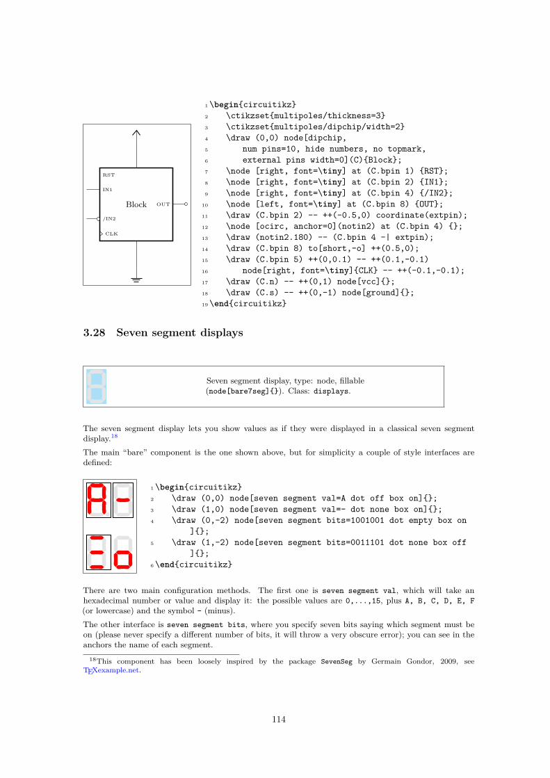
Block
RST
IN1
/IN2
OUT
CLK
1\begincircuitikz2 \ctikzsetmultipoles/thickness=33 \ctikzsetmultipoles/dipchip/width=24 \draw (0,0) node[dipchip,5 num pins=10, hide numbers, no topmark,6 external pins width=0](C)Block;7 \node [right, font=\tiny] at (C.bpin 1) RST;8 \node [right, font=\tiny] at (C.bpin 2) IN1;9 \node [right, font=\tiny] at (C.bpin 4) /IN2;
10 \node [left, font=\tiny] at (C.bpin 8) OUT;11 \draw (C.bpin 2) -- ++(-0.5,0) coordinate(extpin);12 \node [ocirc, anchor=0](notin2) at (C.bpin 4) ;13 \draw (notin2.180) -- (C.bpin 4 -| extpin);14 \draw (C.bpin 8) to[short,-o] ++(0.5,0);15 \draw (C.bpin 5) ++(0,0.1) -- ++(0.1,-0.1)16 node[right, font=\tiny]CLK -- ++(-0.1,-0.1);17 \draw (C.n) -- ++(0,1) node[vcc];18 \draw (C.s) -- ++(0,-1) node[ground];19\endcircuitikz
3.28 Seven segment displays
Seven segment display, type: node, fillable(node[bare7seg]). Class: displays.
The seven segment display lets you show values as if they were displayed in a classical seven segmentdisplay.18
The main “bare” component is the one shown above, but for simplicity a couple of style interfaces aredefined:
1\begincircuitikz2 \draw (0,0) node[seven segment val=A dot off box on];3 \draw (1,0) node[seven segment val=- dot none box on];4 \draw (0,-2) node[seven segment bits=1001001 dot empty box on
];5 \draw (1,-2) node[seven segment bits=0011101 dot none box off
];6\endcircuitikz
There are two main configuration methods. The first one is seven segment val, which will take anhexadecimal number or value and display it: the possible values are 0,...,15, plus A, B, C, D, E, F(or lowercase) and the symbol - (minus).The other interface is seven segment bits, where you specify seven bits saying which segment must beon (please never specify a different number of bits, it will throw a very obscure error); you can see in theanchors the name of each segment.
18This component has been loosely inspired by the package SevenSeg by Germain Gondor, 2009, seeTEXexample.net.
114

The option dot specifies if you want a decimal dot or not. The key none will remove the dot and the spaceit would take; empty will not show the dot at all but reserve the space, and on or off will show the dotin the corresponding state.The option box (can be on or off) simply toggles the drawing of the external box. You can separate itfrom the display with the key seven seg/box sep (default 1pt), and it will use the thickness specified inmultipoles/thickness (The same as the chips).You can use these option with the “bare” object bare7seg and the keys seven seg/bits (default 0000000),seven seg/dot (default none) and seven seg/box (default off); there is no option equivalent to the valinterface.
3.28.1 Seven segments anchors
These are the anchors for the seven segment displays; notice that when the dot parameter is not none,the cell is a bit wider at the right side.
north north east
east
south eastsouthsouth west
west
north west
center
north north east
east
south eastsouth
center
ab
c
de
f
g
dot
3.28.2 Seven segments customization
You can scale the seven segment display with the key displays/scale. This will scale the size of the digit,but not the absolute sizes shown below — if you want them to scale, yo have to do it manually.You can change several parameters to adjust the displays:
1 \ctikzsetseven seg/width/.initial=0.4% relative to \pgf@circ@Rlen (scalable)2 \ctikzsetseven seg/thickness/.initial=4pt% segment thickness (not scaled)3 \ctikzsetseven seg/segment sep/.initial=0.2pt% gap between segments (not scaled)4 \ctikzsetseven seg/box sep/.initial=1pt% external box gap (not scaled)5 \ctikzsetseven seg/color on/.initial=red% color for segment "on"6 \ctikzsetseven seg/color off/.initial=gray!20!white % ...and "off"
A couple of examples are shown below.
1 \begincircuitikz[scale=0.5]2 \ctikzsetseven seg/width=0.2, seven seg/thickness=2pt3 \foreach \i in 0,...,15 \path (\i,0)4 node[seven segment val=\i dot on box off];5 \ctikzsetseven seg/color on=black6 \foreach \i in 0,...,15 \path (\i,-1.5)7 node[seven segment val=\i dot off box off, fill=gray!30!white];8 \ctikzsetseven seg/color on=green, seven seg/color off=yellow!309 \foreach \i in 0,...,15 \path[color=red] (\i,-3)
10 node[seven segment val=\i dot none box on, xslant=0.2];11 \endcircuitikz
115

4 Labels and similar annotations
R11\begincircuitikz2 \draw (0,0) to[R, l=$R_1$] (2,0);3\endcircuitikz
R11\begincircuitikz2 \draw (0,0) to[R=$R_1$] (2,0);3\endcircuitikz
i11\begincircuitikz2 \draw (0,0) to[R, i=$i_1$] (2,0);3\endcircuitikz
v1
1\begincircuitikz2 \draw (0,0) to[R, v=$v_1$] (2,0);3\endcircuitikz
R1
v1
i11\begincircuitikz2 \draw (0,0) to[R=$R_1$, i=$i_1$, v=$v_1$] (2,0);3\endcircuitikz
R1
v1
i11\begincircuitikz2 \draw (0,0) to[R=$R_1$, i=$i_1$, v=$v_1$] (2,0);3\endcircuitikz
Long names/styles for the bipoles can be used:
1 kΩ 1\begincircuitikz\draw2 (0,0) to[resistor=1<\kilo\ohm>] (2,0)3;\endcircuitikz
4.1 Labels and Annotations
Since Version 0.7, beside the original label (l) option, there is a new option to place a second label, calledannotation (a) at each bipole. Up to now this is a beta-test and there can be problems. For example, upto now this option is not compatible with the concurrent use of voltage labels.The position of (a) and (l) labels can be adjusted with _ and , respectively.
R1
1 kΩ
1\begincircuitikz2 \draw (0,0) to[R, l=$R_1$,a=1<\kilo\ohm>] (2,0);3\endcircuitikz
R1
1 kΩ 1\begincircuitikz2 \draw (0,0) to[R, l_=$R_1$,a^=1<\kilo\ohm>] (2,0);3\endcircuitikz
116

Caveat: notice that the way in which circuitikz processes the options, there will be problems if thelabel (or annotation, voltage, or current) contains one of the characters = (equal) or , (comma), givingunexpected errors and wrong output. These two characters must be protected to the option parser usingan \mbox command, or redefining the characters with a TEX \def:
R = 3
R = 3 R, 3
R=31 \def\eq=2 \begincircuitikz3 % the following will fail:4 % \draw (0,0) to[R, l=$R=3] (3,0);5 \draw (0,0) to[R, l=\mbox$R=3$] (3,0);6 \draw (0,0) to[R, l=$R\eq3$] (0,3);7 \draw (3,3) to[R, l=\mbox$R,3$] (3,0);8 % this works, but it has wrong spacing9 \draw (0,3) to[R, l=$R=3$] (3,3);
10 \endcircuitikz
The default orientation of labels is controlled by the options smartlabels, rotatelabels and straightlabels(or the corresponding label/align keys). Here are examples to see the differences:
0
4590
135
180
-90
-45
-135
1\begincircuitikz2\ctikzsetlabel/align = straight3\def\DIR0,45,90,135,180,-90,-45,-1354\foreach \i in \DIR 5 \draw (0,0) to[R=\i, *-o] (\i:2.5);67\endcircuitikz
0
4590
135
180
-90
-45
-135
1\begincircuitikz2\ctikzsetlabel/align = rotate3\def\DIR0,45,90,135,180,-90,-45,-1354\foreach \i in \DIR 5 \draw (0,0) to[R=\i, *-o] (\i:2.5);67\endcircuitikz
117

0
4590135
180
-90
-45
-135
1\begincircuitikz2\ctikzsetlabel/align = smart3\def\DIR0,45,90,135,180,-90,-45,-1354\foreach \i in \DIR 5 \draw (0,0) to[R=\i, *-o] (\i:2.5);67\endcircuitikz
You also can use stacked (two lines) labels. The example should be self-explanatory: the two lines arespecified as l2=line1 and line2. You can use the keys l2 halign to control horizontal position (left,center, right) and l2 valign to control the vertical one (bottom, ccenter, top).
RCC
4.7 kΩ
RCC
4.7 kΩRCC
4.7 kΩ
RCC
4.7 kΩ
1 \begincircuitikz[ american, ]2 %3 % default is l2 halign=l, l2 valign=c4 %5 \draw (0,0) to[R, l2_=$R_CC$ and \SI4.7k\
ohm, , l2 valign=t] (2,0);6 \draw (0,0) to[R, l2_=$R_CC$ and \SI4.7k\
ohm, , ] (0,2);7 \draw (0,0) to[R, l2_=$R_CC$ and \SI4.7k\
ohm, l2 halign=c, l2 valign=b] (-2,0);8 \draw (0,0) to[R, l2_=$R_CC$ and \SI4.7k\
ohm, l2 halign=r, l2 valign=c] (0, -2);9 \endcircuitikz
RCC
4.7 kΩ
RCC
4.7 kΩ
RCC
4.7 kΩRCC
4.7 kΩ
1 \begincircuitikz[ american, ]2 \draw (0,0) to[R, l2^=$R_CC$ and \SI4.7k\
ohm, l2 halign=c, l2 valign=b] (2,0);3 \draw (0,0) to[R, l2^=$R_CC$ and \SI4.7k\
ohm, l2 halign=c, ] (0,2);4 \draw (0,0) to[R, l2^=$R_CC$ and \SI4.7k\
ohm, , l2 valign=t] (-2,0);5 \draw (0,0) to[R, l2^=$R_CC$ and \SI4.7k\
ohm, l2 halign=c, l2 valign=t](0, -3);6 \endcircuitikz
4.2 Currents and voltages
The default direction/sign for currents and voltages in the components is, unfortunately, not standard,and can change across country and sometime across different authors. This unfortunate situation createda bit of confusion in circuitikz across the versions, with several incompatible changes starting fromversion 0.5. From version 0.9.0 onward, the maintainers agreed a new policy for the directions of bipoles’voltages and currents, depending on 4 different possible options:
118

• oldvoltagedirection, or the key style voltage dir=old: Use old way of voltage direction havinga difference between european and american direction, with wrong default labelling for batteries (itwas the default before version 0.5);
• nooldvoltagedirection, or the key style voltage dir=noold: The standard from version 0.5 on-ward, utilize the (German?) standard of voltage arrows in the direction of electric fields (withoutfixing batteries);
• RPvoltages (meaning Rising Potential voltages), or the key style voltage dir=RP: the arrow is indirection of rising potential, like in oldvoltagedirection, but batteries and current sources arefixed so that they follow the passive/active standard: the default direction of v and i are chosen sothat, when both values are positive:
– in passive component, the element is dissipating power;– in active components (generators), the element is generating power.
• EFvoltages (meaning Electric Field voltages), or the key style voltage dir=EF: the arrow is indirection of the electric field, like in nooldvoltagedirection, but batteries are fixed;
Notice that the four styles are designed to be used at the environment level: that is, you should use themat the start of your environment as in \begincircuitikz[voltage dir=old] ... and not as a key forsingle components, in which case the behaviour is not guaranteed.The standard direction of currents, flows and voltages are changed by these options; notice that the defaultdrops in case of passive and active elements is normally different. Take care that in the case of noold andEFvoltages also the currents can switch directions. It is much easier to understand the several behaviorsby looking at the following examples, that have been generated by the code:
1\foreach\element in R, C, D, battery2, V, I, sV, cV, cI%2 \noindent\ttfamily3 \begintabularp2cm4 \element \\ american \\[15pt]5 \element \\ european \\6 \endtabular7 \foreach\mode in old, noold, RP, EF 8 \begintabular@l@9 \multicolumn1cvoltage dir \\
10 \multicolumn1cdir=\mode \\[4pt]11 \begintikzpicture[12 american, voltage dir=\mode,13 ]14 \draw (0,0) to[\element, *-o, v=$v_1$, i=$i_1$, ] (2.5,0);15 \endtikzpicture\\16 \begintikzpicture[17 european, voltage dir=\mode,18 ]19 \draw (0,0) to[\element, *-o, v=$v_1$, i=$i_1$, ] (2.5,0);20 \endtikzpicture21 \endtabular22 \medskip23 24 \par25
119

Ramerican
Reuropean
voltage dirdir=old
+ −v1
i1
v1
i1
voltage dirdir=noold
+ −v1
i1
v1
i1
voltage dirdir=RP
+ −v1
i1
v1
i1
voltage dirdir=EF
+ −v1
i1
v1
i1
Camerican
Ceuropean
voltage dirdir=old
+ −v1
i1
v1
i1
voltage dirdir=noold
+ −v1
i1
v1
i1
voltage dirdir=RP
+ −v1
i1
v1
i1
voltage dirdir=EF
+ −v1
i1
v1
i1
Damerican
Deuropean
voltage dirdir=old
+ −v1
i1
v1
i1
voltage dirdir=noold
+ −v1
i1
v1
i1
voltage dirdir=RP
+ −v1
i1
v1
i1
voltage dirdir=EF
+ −v1
i1
v1
i1
battery2american
battery2european
voltage dirdir=old
+ −v1
i1
v1
i1
voltage dirdir=noold
+ −v1
i1
v1
i1
voltage dirdir=RP
− +v1
i1
v1
i1
voltage dirdir=EF
− +v1
i1
v1
i1
Vamerican
Veuropean
voltage dirdir=old
+−
v1
i1
v1
i1
voltage dirdir=noold
−+
v1
i1
v1
i1
voltage dirdir=RP
+−
v1
i1
v1
i1
voltage dirdir=EF
−+
v1
i1
v1
i1
120

Iamerican
Ieuropean
voltage dirdir=old
+ −v1
i1
v1
i1
voltage dirdir=noold
− +v1
i1
v1
i1
voltage dirdir=RP
− +v1
i1
v1
i1
voltage dirdir=EF
− +v1
i1
v1
i1
sVamerican
sVeuropean
voltage dirdir=old
+ −v1
i1
v1
i1
voltage dirdir=noold
+ −v1
i1
v1
i1
voltage dirdir=RP
− +v1
i1
v1
i1
voltage dirdir=EF
− +v1
i1
v1
i1
cVamerican
cVeuropean
voltage dirdir=old
+−
v1
i1
v1
i1
voltage dirdir=noold
−+
v1
i1
v1
i1
voltage dirdir=RP
+−
v1
i1
v1
i1
voltage dirdir=EF
−+
v1
i1
v1
i1
cIamerican
cIeuropean
voltage dirdir=old
+ −v1
i1
v1
i1
voltage dirdir=noold
− +v1
i1
v1
i1
voltage dirdir=RP
− +v1
i1
v1
i1
voltage dirdir=EF
− +v1
i1
v1
i1
Obviously, you normally use just one between current and flows, but anyway you can change directionof the voltages, currents and flows using the complete keys i_>, i^<, i>_, i>^, as shown in the followingexamples.This manual has been typeset with the option RPvoltages.
121

4.3 Currents
Inline (along the wire) currents are selected with i_>, i^<, i>_, i>^, and various simplification; the defaultposition and direction is obtained with the key i=....
i11\begincircuitikz2 \draw (0,0) to[R, i^>=$i_1$] (2,0);3\endcircuitikz
i1
1\begincircuitikz2 \draw (0,0) to[R, i_>=$i_1$] (2,0);3\endcircuitikz
i11\begincircuitikz2 \draw (0,0) to[R, i^<=$i_1$] (2,0);3\endcircuitikz
i1
1\begincircuitikz2 \draw (0,0) to[R, i_<=$i_1$] (2,0);3\endcircuitikz
i11\begincircuitikz2 \draw (0,0) to[R, i>^=$i_1$] (2,0);3\endcircuitikz
i1
1\begincircuitikz2 \draw (0,0) to[R, i>_=$i_1$] (2,0);3\endcircuitikz
i11\begincircuitikz2 \draw (0,0) to[R, i<^=$i_1$] (2,0);3\endcircuitikz
i1
1\begincircuitikz2 \draw (0,0) to[R, i<_=$i_1$] (2,0);3\endcircuitikz
Also:
i11\begincircuitikz2 \draw (0,0) to[R, i<=$i_1$] (2,0);3\endcircuitikz
i11\begincircuitikz2 \draw (0,0) to[R, i>=$i_1$] (2,0);3\endcircuitikz
i11\begincircuitikz2 \draw (0,0) to[R, i^=$i_1$] (2,0);3\endcircuitikz
122

i1
1\begincircuitikz2 \draw (0,0) to[R, i_=$i_1$] (2,0);3\endcircuitikz
10V
i1
1\begincircuitikz2 \draw (0,0) to[V=10V, i_=$i_1$] (2,0);3\endcircuitikz
10V
i1
1\begincircuitikz2 \draw (0,0) to[V<=10V, i_=$i_1$] (2,0);3\endcircuitikz
+−
10V
i1
1\begincircuitikz[american]2 \draw (0,0) to[V=10V, i_=$i_1$] (2,0);3\endcircuitikz
+ −
10V
i1
1\begincircuitikz[american]2 \draw (0,0) to[V=10V,invert, i_=$i_1$] (2,0);3\endcircuitikz
1A
i1
1\begincircuitikz[american]2 \draw (0,0) to[dcisource=1A, i_=$i_1$] (2,0);3\endcircuitikz
1A
i1
1\begincircuitikz[american]2 \draw (0,0) to[dcisource=1A,invert, i_=$i_1$] (2,0);3\endcircuitikz
4.4 Flows
As an alternative for the current arrows, you can also use the following flows. They can also be used toindicate thermal or power flows. The syntax is pretty the same as for currents.This is a new beta feature since version 0.8.3; therefore, please provide bug reports or hints to optimize thisfeature regarding placement and appearance! This means that the appearance may change in the future!
i11\begincircuitikz2 \draw (0,0) to[R, f=$i_1$] (3,0);3\endcircuitikz
i11\begincircuitikz2 \draw (0,0) to[R, f<=$i_1$] (3,0);3\endcircuitikz
i1
1\begincircuitikz2 \draw (0,0) to[R, f_=$i_1$] (3,0);3\endcircuitikz
123

i1
1\begincircuitikz2 \draw (0,0) to[R, f_>=$i_1$] (3,0);3\endcircuitikz
i11\begincircuitikz2 \draw (0,0) to[R, f<^=$i_1$] (3,0);3\endcircuitikz
i1
1\begincircuitikz2 \draw (0,0) to[R, f<_=$i_1$] (3,0);3\endcircuitikz
i1
1\begincircuitikz2 \draw (0,0) to[R, f>_=$i_1$] (3,0);3\endcircuitikz
4.5 Voltages
See introduction note at Currents (chapter 4.2, page 118)!
4.5.1 European style
The default, with arrows. Use option europeanvoltage or style [european voltages].
v1 1\begincircuitikz[european voltages]2 \draw (0,0) to[R, v^>=$v_1$] (2,0);3\endcircuitikz
v1 1\begincircuitikz[european voltages]2 \draw (0,0) to[R, v^<=$v_1$] (2,0);3\endcircuitikz
v1
1\begincircuitikz[european voltages]2 \draw (0,0) to[R, v_>=$v_1$] (2,0);3\endcircuitikz
v1
1\begincircuitikz[european voltages]2 \draw (0,0) to[R, v_<=$v_1$] (2,0);3\endcircuitikz
10V
i1
1\begincircuitikz2 \draw (0,0) to[V=10V, i_=$i_1$] (2,0);3\endcircuitikz
10V
i1
1\begincircuitikz2 \draw (0,0) to[V<=10V, i_=$i_1$] (2,0);3\endcircuitikz
124

u1
1A 1\begincircuitikz2 \draw (0,0) to[I=1A, v_=$u_1$] (2,0);3\endcircuitikz
u1
1A 1\begincircuitikz2 \draw (0,0) to[I<=1A, v_=$u_1$] (2,0);3\endcircuitikz
1A
u1
1\begincircuitikz2 \draw (0,0) to[I=$~$,l=1A, v_=$u_1$] (2,0);3\endcircuitikz
1A
u1
1\begincircuitikz2 \draw (0,0) to[I,l=1A, v_=$u_1$] (2,0);3\endcircuitikz
1V
u1
i1 1\begincircuitikz2 \draw (0,0) to[battery,l_=1V, v=$u_1$, i=$i_1$] (2,0);3\endcircuitikz
4.5.2 American style
Use option americanvoltage or set [american voltages].
− +v1
1\begincircuitikz[american voltages]2 \draw (0,0) to[R, v^>=$v_1$] (2,0);3\endcircuitikz
+ −v11\begincircuitikz[american voltages]2 \draw (0,0) to[R, v^<=$v_1$] (2,0);3\endcircuitikz
− +v1
1\begincircuitikz[american voltages]2 \draw (0,0) to[R, v_>=$v_1$] (2,0);3\endcircuitikz
+ −v1
1\begincircuitikz[american voltages]2 \draw (0,0) to[R, v_<=$v_1$] (2,0);3\endcircuitikz
− +u1
1A 1\begincircuitikz[american]2 \draw (0,0) to[I=1A, v_=$u_1$] (2,0);3\endcircuitikz
− +
i1
1A 1\begincircuitikz[american]2 \draw (0,0) to[I<=1A, v_=$i_1$] (2,0);3\endcircuitikz
125

4.5.3 Voltage position
It is possible to move away the arrows and the plus or minus signs with the key voltages shift (defaultvalue is 0, which gives the standard position):
v1
i1
v1
i1
v1
i1
1\begincircuitikz[]2 \draw (0,0) to[R, v=$v_1$, i=$i_1$] (2,0);3 \draw (0,-1) to[R, v=$v_1$, i=$i_1$,4 voltage shift=0.5] (2,-1);5 \draw (0,-2) to[R, v=$v_1$, i=$i_1$,6 voltage shift=1.0, ] (2,-2);7\endcircuitikz
+ −v1
i11\begincircuitikz[american voltages, voltage shift=0.5]2 \draw (0,0) to[R, v=$v_1$, i=$i_1$] (2,0);3\endcircuitikz
Notes that american voltage also affects batteries.
1V
u1
i11 \begincircuitikz[voltage shift=0.5]2 \draw (0,0) to[battery,l_=1V, v=$u_1$, i=$i_1$] (2,0);3\endcircuitikz
1V
− +u1
i11\begincircuitikz[american voltages, voltage shift=0.5]2 \draw (0,0) to[battery,l_=1V, v=$u_1$, i=$i_1$] (2,0);3\endcircuitikz
4.5.4 American voltages customization
Since 0.9.0, you can change the font19 used by the american voltages style, by setting to somethingdifferent from nothing the key voltage/american font (default: nothing, using the current font) style:
+ −VS
+ −VS
1\begincircuitikz[american]2 \beginscope3 \ctikzsetvoltage/american font=\tiny\boldmath4 \draw (0,0) to[R,v=$V_S$] ++(2,0);5 \endscope6 \draw (0,-2) to[R,v=$V_S$] ++(2,0);7\endcircuitikz
Also, if you want to change the symbols (sometime just the + sign is drawn, for example, or for highlightingsomething), using the keys voltage/american plus and voltage/american minus (default $+$ and $-$).
19There where a bug before, noticed by the user dzereb on tex.stackexchange.com which made the symbols usingdifferent fonts in a basically random way. In the same page, user campa found the problem. Thanks!
126

⊖ ⊕VS
⊕ ⊖VS
1\begincircuitikz[american]2 \ctikzsetvoltage/american font=\scriptsize\boldmath3 \ctikzsetvoltage/american plus=\textcolorred$\oplus$4 \ctikzsetvoltage/american minus=\textcolorblue$\ominus$5 \draw (0,0) to[R,v_>=$V_S$] ++(2,0);6 \draw (0,-2) to[R,v_<=$V_S$] ++(2,0);7\endcircuitikz
This could be especially useful if you define a style, to use like this:
− +VS
+ −VS
1\tikzsetred plus/.style=2 circuitikz/voltage/american plus=\textcolorred$+$,34\begincircuitikz[american]5 \draw (0,0) to[R,v_>=$V_S$, red plus] ++(2,0);6 \draw (0,-2) to[R,v_<=$V_S$] ++(2,0);7\endcircuitikz
4.6 Global properties of voltages and currents
1V
1V
1\tikz \draw (0,0) to[R, v=1<\volt>] (2,0); \par2\ctikzsetvoltage/distance from node=.13\tikz \draw (0,0) to[R, v=1<\volt>] (2,0);
ı
ı
1\tikz \draw (0,0) to[C, i=$\imath$] (2,0); \par2\ctikzsetcurrent/distance = .23\tikz \draw (0,0) to[C, i=$\imath$] (2,0);
However, you can override the properties voltage/distance from node (how distant from the initial andfinal points of the path the arrow starts and ends) and voltage/bump b (how high the bump of the arrowis — how curved it is)20 on a per-component basis, in order to fine-tune the voltages:
1V2V
1V2V
1\tikz \draw (0,0) to[R, v=1<\volt>] (1.5,0)2 to[C, v=2<\volt>] (3,0); \par3\ctikzsetbipoles/capacitor/voltage/distance from node/.
initial=.74\tikz \draw (0,0) to[R, v=1<\volt>] (1.5,0)5 to[C, v=2<\volt>] (3,0); \par
Note the .initial; you have to create such key the first time you use it.20Prior to 0.9.4 you had also voltage/european label distance (how distant from the bipole the voltage label
will be) but this is deprecated, and the european-style label is printed near the bump)
127

4.7 Changing the style of labels and text ornaments
Since version 0.9.5, it is possible to change the style of bipole text ornaments (labels, annotations,voltages etc) by using the appropriate styles or keys. The basic style applied to the text are defined in the/tikz/circuitikz key directory and applied to every node that contains the text; you can also changethem locally by using the tikz direct keys in local scopes.For example, you can make all annotations small by using:
\ctikzsetbipole annotation style/.style=font=\small
And the change (override) the setting in one specific bipole using:
...to[bipole annotation style=color=red, R, a=Red note]...
where the annotation will be in normal font (it has been reset!) and red, or append to the style:
...to[bipole annotation append style=color=red, R, a=Red small note]...
Caveat: you have to put the style changing key at the start of the to arguments to have any effect21.The available styles and commands are bipole label style, bipole annotation style, bipole voltagestyle, bipole current style, and bipole flow style. The following example shows a bit of everything.
L1
A1 L22L
A2 R1
+ −V1
I1F1
+ −V2
I2F2
1 \begincircuitikz[american]2 \ctikzsetbipole annotation style/.style=font=\tiny3 \ctikzsetbipole current style/.style=font=\small\sffamily4 \draw (0,0) to [bipole annotation append style=fill=yellow, R=L1, a=A1] ++(3,0)5 to [bipole label style=fill=cyan, R, l2_=L2 and 2L, a^=A2] ++(3,0);6 \draw (7,0) to [bipole voltage style=color=blue,7 bipole flow style=fill=green, outer sep=5pt,8 R=R1, v=V1, i=I1, f>^=F1] ++(3,0)9 to [bipole current append style=color=red, R, v<=V2, i^=I2, f>^=F2] ++(3,0);
10 \endcircuitikz
4.8 Labels in special components
For some components label, current and voltage behave as one would expect:
a11\begincircuitikz2 \draw (0,0) to[I=$a_1$] (2,0);3\endcircuitikz
a11\begincircuitikz2 \draw (0,0) to[I, i=$a_1$] (2,0);3\endcircuitikz
k · a11\begincircuitikz2 \draw (0,0) to[cI=$k\cdot a_1$] (2,0);3\endcircuitikz
21No, I do not know why. Hints and fixes are welcome.
128

a11\begincircuitikz2 \draw (0,0) to[sI=$a_1$] (2,0);3\endcircuitikz
k · a11\begincircuitikz2 \draw (0,0) to[csI=$k\cdot a_1$] (2,0);3\endcircuitikz
The following results from using the option americancurrent or using the style [american currents].
a11\begincircuitikz[american currents]2 \draw (0,0) to[I=$a_1$] (2,0);3\endcircuitikz
a11\begincircuitikz[american currents]2 \draw (0,0) to[I, i=$a_1$] (2,0);3\endcircuitikz
k · a11\begincircuitikz[american currents]2 \draw (0,0) to[cI=$k\cdot a_1$] (2,0);3\endcircuitikz
a11\begincircuitikz[american currents]2 \draw (0,0) to[sI=$a_1$] (2,0);3\endcircuitikz
k · a11\begincircuitikz[american currents]2 \draw (0,0) to[csI=$k\cdot a_1$] (2,0);3\endcircuitikz
The same holds for voltage sources:
a1 1\begincircuitikz2 \draw (0,0) to[V=$a_1$] (2,0);3\endcircuitikz
a1 1\begincircuitikz2 \draw (0,0) to[V, v=$a_1$] (2,0);3\endcircuitikz
k · a1 1\begincircuitikz2 \draw (0,0) to[cV=$k\cdot a_1$] (2,0);3\endcircuitikz
a1 1\begincircuitikz2 \draw (0,0) to[sV=$a_1$] (2,0);3\endcircuitikz
129

k · a1 1\begincircuitikz2 \draw (0,0) to[csV=$k\cdot a_1$] (2,0);3\endcircuitikz
The following results from using the option americanvoltage or the style [american voltages].
+−
a1 1\begincircuitikz[american voltages]2 \draw (0,0) to[V=$a_1$] (2,0);3\endcircuitikz
+−
a1 1\begincircuitikz[american voltages]2 \draw (0,0) to[V, v=$a_1$] (2,0);3\endcircuitikz
+−
kve 1\begincircuitikz[american voltages]2 \draw (0,0) to[cV=$k v_e$] (2,0);3\endcircuitikz
− +a1 1\begincircuitikz[american voltages]
2 \draw (0,0) to[sV=$a_1$] (2,0);3\endcircuitikz
− +kve 1\begincircuitikz[american voltages]
2 \draw (0,0) to[csV=$k v_e$] (2,0);3\endcircuitikz
4.9 Integration with siunitx
If the option siunitx is active (and not in ConTEXt), then the following are equivalent:
1 kΩ 1\begincircuitikz2 \draw (0,0) to[R, l=1<\kilo\ohm>] (2,0);3\endcircuitikz
1 kΩ 1\begincircuitikz2 \draw (0,0) to[R, l=$\SI1\kilo\ohm$] (2,0);3\endcircuitikz
1mA1\begincircuitikz2 \draw (0,0) to[R, i=1<\milli\ampere>] (2,0);3\endcircuitikz
1mA1\begincircuitikz2 \draw (0,0) to[R, i=$\SI1\milli\ampere$] (2,0);3\endcircuitikz
130

1V
1\begincircuitikz2 \draw (0,0) to[R, v=1<\volt>] (2,0);3\endcircuitikz
1V
1\begincircuitikz2 \draw (0,0) to[R, v=$\SI1\volt$] (2,0);3\endcircuitikz
4.10 Accessing labels text nodes
Since 0.9.5, you can access all the labels nodes22 using special node names. So, if you use name to give aname to the bipole node, you can access also the following nodes: namelabel (notice: no space nor anyother symbol between name and label!), nameannotation, namevoltage, namecurrent and nameflow.
L1
A1 L22L
A2L1
L1label
L1annotation
L2
L2label
L2annotation
R1
+ −V1
I1F1
+ −V2
I2F2
R1voltage R2voltage
R1current R2currentR1flow R2flow
1 \newcommand\marknode[2][45]%2 \node[circle, draw, red, inner sep=1pt,3 pin=[red, font=\tiny]#1:#2] at (#2.center) ;4 5 \begincircuitikz[ american]6 \draw (0,0) to [R=L1, a=A1, name=L1] ++(3,0)7 to [R, l2_=L2 and 2L, a^=A2, name=L2] ++(3,0);8 \marknodeL1 \marknodeL1label \marknode[0]L1annotation9 \marknodeL2 \marknode[0]L2label \marknodeL2annotation
10 \draw[blue] (L2label.south west) rectangle (L2label.north east);11 \draw (6.1,0) to [R=R1, v=V1, i=I1, f>^=F1, name=R1] ++(3,0)12 to [R, v<=V2, i^=I2, f>^=F2, name=R2] ++(3,0);13 \marknode[0]R1voltage \marknode[0]R2voltage \marknode[90]R1current14 \marknode[90]R2current \marknodeR1flow \marknodeR2flow15 \endcircuitikz
22The access to labels and annotations was present before, but not documented.
131

5 Using bipoles in circuits
5.1 Nodes (also called poles)
You can add nodes to the bipoles, positioned at the coordinates surrounding the component. The gen-eral style to use is bipole nodes=startstop, where start and stop are the nodes — to be chosenbetween none, circ, ocirc, squarepole, osquarepole, diamondpole, odiamondpole and rectfill23 (seesection 3.15).
nonecirc
ocirc
diamondpole
odiamondpole
squarepoleosquarepole
1 \begincircuitikz2 \ctikzsetbipoles/length=.5cm, nodes width=0.1%small
components, big nodes3 \foreach \a/\p [evaluate=\a as \b using (\a+180)] in4 -90/none, -60/circ, -30/ocirc, 0/diamondpole, 30/
odiamondpole, 60/squarepole, 90/osquarepole5 \draw (0,0) to[R, bipole nodes=none\p] ++(\a:1.5)
node[font=\tiny, anchor=\b]\p;6 \endcircuitikz
These bipole nodes are added after the path is drawn, as every node in TikZ — this is the reason why theyare always filled (with the main color the normal nodes, with white the open ones), in order to “hide” thewire below. You can override the fill color if you want; but notice that if you draw things in two differentpaths, you will have “strange” results; notice that in the second line of resistors the second wire is startingfrom the center of the white ocirc of the previous path.
1 \begincircuitikz2 \draw (0,0) to[R, *-o] ++(2,0) to[R, -d] ++(2,0)3 to[R, bipole nodes=diamondpoleodiamondpole, fill=red] ++(2,0);4 \draw (0,-1) to[R, *-o] ++(2,0) ;5 \draw (2,-1) to[R, -d] ++(2,0) to[R, bipole nodes=nonesquarepole] ++(2,0);6 \endcircuitikz
You can define shortcuts for the bipole nodes you use most; for example if you want a shortcut for abipole with open square node in red in the right side you can:
1 \begincircuitikz2 \ctikzset-s/.style = bipole nodes=noneosquarepole, fill=red3 \draw (0,0) to[R, -s] ++(2,0);4 \endcircuitikz
There are several predefined shorthand as the above; in the following pages you can see all of them.
1\begincircuitikz2 \draw (0,0) to[R, o-o] (2,0);3\endcircuitikz
23You can use other shapes too, but at your own risk…Moreover, notice that none is not really a node, just aspecial word used to say “do not put any node here”.
132

1\begincircuitikz2 \draw (0,0) to[R, -o] (2,0);3\endcircuitikz
1\begincircuitikz2 \draw (0,0) to[R, o-] (2,0);3\endcircuitikz
1\begincircuitikz2 \draw (0,0) to[R, *-*] (2,0);3\endcircuitikz
1\begincircuitikz2 \draw (0,0) to[R, -*] (2,0);3\endcircuitikz
1\begincircuitikz2 \draw (0,0) to[R, *-] (2,0);3\endcircuitikz
1\begincircuitikz2 \draw (0,0) to[R, d-d] (2,0);3\endcircuitikz
1\begincircuitikz2 \draw (0,0) to[R, -d] (2,0);3\endcircuitikz
1\begincircuitikz2 \draw (0,0) to[R, d-] (2,0);3\endcircuitikz
1\begincircuitikz2 \draw (0,0) to[R, o-*] (2,0);3\endcircuitikz
1\begincircuitikz2 \draw (0,0) to[R, *-o] (2,0);3\endcircuitikz
1\begincircuitikz2 \draw (0,0) to[R, o-d] (2,0);3\endcircuitikz
1\begincircuitikz2 \draw (0,0) to[R, d-o] (2,0);3\endcircuitikz
1\begincircuitikz2 \draw (0,0) to[R, *-d] (2,0);3\endcircuitikz
1\begincircuitikz2 \draw (0,0) to[R, d-*] (2,0);3\endcircuitikz
133

5.1.1 Transparent poles
“Open-poles” terminals (ocirc, odiamondpole, and osquarepole) are normally filled with the backgroundcolor at full opacity. This is because, for simplicity of operation, the nodes are placed after the wires aredrawn and have to “white-out” the underlying lines.Anyway, if you know what you are doing, you can change it with the key poles/open fill opacity (with\ctikzset) or the style open poles opacity. Notice that you will have artifacts if you don’t use theborder anchors of the poles to connect wires, and you need to do that by hand.
1 \begincircuitikz[scale=3, transform shape]2 \fill[cyan] (0,0) rectangle (4.1,-0.6);3 \tikzsethalfwhite/.style=fill opacity=0.5, fill=white, open poles opacity=0.54 % automatic positioning when opacity is not 1.0 creates artifacts5 \draw[halfwhite] (0,0) to[generic, -o] ++(2,0) --++(0,-0.5);6 % you have to use manual positioning7 \draw[halfwhite] (2.2,0) -- ++(0.5,0) node[ocirc, anchor=180];8 \draw[halfwhite] (3,0) node[ocirc](B) (B.0) --++(0.5,0) (B.-90) --++(0,-0.5);9 % maybe really useful only for terminals going out of the circuit...
10 \draw (3.6,0) -- ++(0.2,0) node[ocirc, halfwhite, anchor=180];11 \endcircuitikz
You also have the similar keys for the “full” poles (albeit they are probably not useful at all).
5.2 Mirroring and InvertingBipole paths can also mirrored and inverted (or reverted) to change the drawing direction.
1\begincircuitikz2 \draw (0,0) to[pD] (2,0);3\endcircuitikz
1\begincircuitikz2 \draw (0,0) to[pD, mirror] (2,0);3\endcircuitikz
1\begincircuitikz2 \draw (0,0) to[pD, invert] (2,0);3\endcircuitikz
Placing labels, currents and voltages works also, please note, that mirroring and inverting does not influ-ence the positioning of labels and voltages. Labels are by default above/right of the bipole and voltagesbelow/left, respectively.
T
v
i11\begincircuitikz2 \draw (0,0) to[ospst=T, i=$i_1$, v=$v$] (2,0);3\endcircuitikz
134

T
v
i1 1\begincircuitikz2 \draw (0,0) to[ospst=T, mirror, i=$i_1$, v=$v$] (2,0);3\endcircuitikz
T
v
i11\begincircuitikz2 \draw (0,0) to[ospst=T, invert, i=$i_1$, v=$v$] (2,0);3\endcircuitikz
T
v
i1 1\begincircuitikz2 \draw (0,0) to[ospst=T,mirror,invert, i=$i_1$, v=$v$] (2,0);3\endcircuitikz
5.3 Putting them together
1 kΩ
1mA
1\begincircuitikz2 \draw (0,0) to[R=1<\kilo\ohm>,3 i>_=1<\milli\ampere>, o-*] (3,0);4\endcircuitikz
vD
1mA 1\begincircuitikz2 \draw (0,0) to[D*, v=$v_D$,3 i=1<\milli\ampere>, o-*] (3,0);4\endcircuitikz
5.4 Line joins between Path Components
Line joins should be calculated correctly - if they are on the same path, and the path is not closed. Forexample, the following path is not closed correctly (–cycle does not work here!):
1 \begintikzpicture[line width=3pt,european]2 \draw (0,0) to[R]++(2,0)to[R]++(0,2)3 --++(-2,0)to[R]++(0,-2);4 \draw[red,line width=1pt] circle(2mm);5 \endtikzpicture
To correct the line ending, there are support shapes to fill the missing rectangle. They can be used likethe support shapes (*,o,d) using a dot (.) on one or both ends of a component (have a look at the lastresistor in this example:
1 \begintikzpicture[line width=3pt,european]2 \draw (0,0) to[R]++(2,0)to[R]++(0,2)3 --++(-2,0)to[R,-.]++(0,-2);4 \draw[red,line width=1pt] circle(2mm);5 \endtikzpicture
135

6 Colors
6.1 Shape colors
The color of the components is stored in the key \circuitikzbasekey/color. CircuiTikZ tries to followthe color set in TikZ, although sometimes it fails. If you change color in the picture, please do not usejust the color name as a style, like [red], but rather assign the style [color=red].Compare for instance
1\begincircuitikz \draw[red]2 (0,2) node[and port] (myand1) 3 (0,0) node[and port] (myand2) 4 (2,1) node[xnor port] (myxnor) 5 (myand1.out) -| (myxnor.in 1)6 (myand2.out) -| (myxnor.in 2)7;\endcircuitikz
and
1\begincircuitikz \draw[color=red]2 (0,2) node[and port] (myand1) 3 (0,0) node[and port] (myand2) 4 (2,1) node[xnor port] (myxnor) 5 (myand1.out) -| (myxnor.in 1)6 (myand2.out) -| (myxnor.in 2)7;\endcircuitikz
One can of course change the color in medias res:
1\begincircuitikz \draw2 (0,0) node[pnp, color=blue] (pnp2) 3 (pnp2.B) node[pnp, xscale=-1, anchor=B, color=brown] (pnp1) 4 (pnp1.C) node[npn, anchor=C, color=green] (npn1) 5 (pnp2.C) node[npn, xscale=-1, anchor=C, color=magenta] (npn2) 6 (pnp1.E) -- (pnp2.E) (npn1.E) -- (npn2.E)7 (pnp1.B) node[circ] |- (pnp2.C) node[circ] 8;\endcircuitikz
The all-in-one stream of bipoles poses some challanges, as only the actual body of the bipole, and not theconnecting lines, will be rendered in the specified color. Also, please notice the curly braces around theto:
136

1V
1Ω
1F
1\begincircuitikz \draw2 (0,0) to[V=1<\volt>] (0,2)3 to[R=1<\ohm>, color=red] (2,2) 4 to[C=1<\farad>] (2,0) -- (0,0)5;\endcircuitikz
Which, for some bipoles, can be frustrating:
1V
1Ω
1F
1\begincircuitikz \draw2 (0,0)to[V=1<\volt>, color=red] (0,2) 3 to[R=1<\ohm>] (2,2)4 to[C=1<\farad>] (2,0) -- (0,0)5;\endcircuitikz
The only way out is to specify different paths:
1V
1Ω
1F
1\begincircuitikz \draw[color=red]2 (0,0) to[V=1<\volt>, color=red] (0,2);3 \draw (0,2) to[R=1<\ohm>] (2,2)4 to[C=1<\farad>] (2,0) -- (0,0)5;\endcircuitikz
And yes: this is a bug and not a feature…
6.2 Fill colorsSince version 0.9.0, you can also fill most shapes with a color (the manual specifies which ones are fillableor not). The syntax is quite intuitive:
1\begincircuitikz \draw2 (0,2) node[and port, fill=yellow] (myand1) 3 (0,0) node[and port, fill=cyan] (myand2) 4 (2,1) node[xnor port,fill=red!30!white] (myxnor) 5 (myand1.out) -| (myxnor.in 1)6 (myand2.out) -| (myxnor.in 2)7;\endcircuitikz
This fill color will override any color defined by the style (see section 3.3.2). If you want to override a stylefill color with no-fill for a specific component, you need to override the style — it’s a bit unfortunate butit should be an exceptional thing anyway:
1 \begincircuitikz2 \ctikzsetlogic ports/fill=cyan!30!white3 \draw[red] (-0.5,3) -- (-0.5, -1);4 \draw[red] (1.5,3) -- (1.5, -1);5 \draw6 (0,2) node[and port, ] (myand1) 7 (0,0) node[and port, fill=cyan] (myand2) 8 (2,1) node[xnor port, circuitikz/logic ports/fill=none] (
myxnor) 9 (myand1.out) -| (myxnor.in 1)
10 (myand2.out) -| (myxnor.in 2)11 ;\endcircuitikz
137

You can combine shape colors with fill colors, too, but you should use the draw color option style for this:
1
2
3
1\begincircuitikz \draw[color=red]2 (0,2) node[and port, fill=yellow] (myand1) 13 (0,0) node[and port, fill=cyan] (myand2) 24 (2,1) node[xnor port,fill=red!30!white] (myxnor) 35 (myand1.out) -| (myxnor.in 1)6 (myand2.out) -| (myxnor.in 2)7;\endcircuitikz
This is because, as you can see from the following example in port 2, you can’t specify both a fill anda color in the node (yes, it’s a bug too, but it’s quite complex to solve given the current circuitTikZarchitecture). A workaround is shown in port 3:
1
2
3
1\begincircuitikz \draw2 (0,2) node[and port, color=black] (myand1) 13 (0,0) node[and port, color=blue, fill=cyan] (myand2)
24 (2,1) [color=blue] node[xnor port, fill=cyan] (myxnor
) 35 (myand1.out) -| (myxnor.in 1)6 (myand2.out) -| (myxnor.in 2)7;\endcircuitikz
Notice also that the connection point are always filled, although the color tries to follow the color of thefilling of the component:
1\begincircuitikz2 \fill[cyan] (0,3.0) rectangle (7,7);3 \draw [fill=yellow, ] (4,4) to [D,o-o] ++(0,2) to[D*, fill=yellow] ++(2,0)4 to[D*] ++(0,-2) to[D, fill=red, o-o] ++(-2,0);5 \draw (1,4) node[ocirc] -- ++(1,0) node[ocirc];6 \draw (1,4.5) to[short, o-o] ++(1,0) to[short, -o] ++(1,0);7 \draw[fill=yellow] (1,5) to[short, o-o] ++(1,0) to[short, -o] ++(1,0);8 \draw (1,5.5) to[short, fill=red, o-o] ++(1,0) to[short, -o] ++(1,0);9\endcircuitikz
138

7 FAQ
Q: When using \tikzexternalize I get the following error:
! Emergency stop.
A: The TikZ manual states:
Furthermore, the library assumes that all LATEX pictures are ended with\endtikzpicture.
Just substitute every occurrence of the environment circuitikz with tikzpicture. They are actuallypretty much the same.
Q: How do I draw the voltage between two nodes?A: Between any two nodes there is an open circuit!
v
1\begincircuitikz \draw2 node[ocirc] (A) at (0,0) 3 node[ocirc] (B) at (2,1) 4 (A) to[open, v=$v$] (B)5;\endcircuitikz
Q: I cannot write to[R = $R_1=12V$] nor to[ospst = open, 3s]: I get errors.A: It is a limitation of the parser.Use \def\eq= to[R = $R_1\eq 12V$] and to[ospst = open, 3s] instead; see caveat in section 4.1.
Q: I tried to change the direction of the y axis with yscale=-1, but the circuit is completely messed up.A: Yes, it’s a known bug (or misfeature, or limitation). See section 1.7. Don’t do that.
Q: I tried to put a diode in a pic, but it’s coming out badly rotated.A: Yes, it’s a known bug (or misfeature, or limitation). See section 1.7. CircuiTikZ is not compatible withpics at this point.
139

8 Defining new components
Per me si va ne la città dolente,per me si va ne l’etterno dolore,per me si va tra la perduta gente.…Lasciate ogne speranza, voi ch’intrate.24
Big fat warning: this material is reserved to TEX-hackers; do not delve into this if you have no familiaritywith (at least) a bit of core TEX programming and to the basic TikZ layer. You have been warned.
8.1 Suggested setup
The suggested way to start working on a new component is to use the utilities of the CircuiTikZ manualfor checking and testing your device. Basically, find (or download) the source code of the last version ofCircuiTikZ and find the file ctikzmanutils.sty; copy it in your directory and prepare a file like this:
1\documentclass[a4paper, titlepage]article2\usepackagea4wide %smaller borders3\usepackage[utf8]inputenc4\usepackage[T1]fontenc5\parindent=0pt6\parskip=4pt plus 6pt minus 2pt7\usepackage[siunitx, RPvoltages]circuitikzgit8\usepackagectikzmanutils9\makeatletter
10 %% Test things here11 % defines12
13 % components14
15 % paths16\makeatother17
18\begindocument19
20\circuitdescbip*damperMechanical damping(left/135/0.2, right/45/0.2,center/-90/0.3)
21
22\geolrcoorddampershape, fill=yellow23
24\beginLTXexample[varwidth]25\begincircuitikz26 \draw (0,0) to[R] ++(2,0)27 to[damper] ++(2,0);28\endcircuitikz29\endLTXexample30\enddocument
This will compile to something like this (in this case, we are using a couple of existing components tocheck everything is ok):
24https://classicsincontext.wordpress.com/2010/02/28/canto-iii-per-me-si-va-ne-la-citta-dolente/
140

left right
center
damper: Mechanical damping, type: path-style, fillable,nodename: dampershape. Class: mechanicals.
text
north north east
east
south eastsouthsouth west
west
north westleft right
center
1\begincircuitikz2 \draw (0,0) to[R] ++(2,0)3 to[damper] ++(2,0);4\endcircuitikz
The command circuitdescbip* is used to show the component description (you can check the definitionand the usage looking at ctikzmanutils.sty file, and the \geolrcoord is used to show the main anchors(geographical plus left and right) of the component.From now on, you can add the new commands for the component between the \makeatletter and\makeatother commands and, modifying the example, check the results.
8.2 Path-style component
Let’s define for example a path style component, like the one suggested by the user @alex on TEX stack-exchange site. The component will be a mix of the damper and the spring components already present.The first step is to check if we can use the definition already existing for similar elements (for coherenceof size) or if we need to define new ones; for this you have to check the file pgfcirc.defines.tex: we find
1 \ctikzsetbipoles/spring/height/.initial=.52 \ctikzsetbipoles/spring/width/.initial=.53 \ctikzsetbipoles/damper/height/.initial=.354 \ctikzsetbipoles/damper/length/.initial=.35 \ctikzsetbipoles/damper/width/.initial=.4
We will use them; at this stage you can decide to add other parameters if you need them. (Notice, however,than although flexibility is good, these parameters should be described in the manual, otherwise they’reas good as a fixed number in the code).To define the new component we will look into pgfcircbipoles.tex and we will copy, for example, thedefinition of the damper into our code, just changing the name:
1 %% mechanical resistor - damper2\pgfcircdeclarebipolescaledmechanicals3 % extra anchors4\ctikzvalofbipoles/damper/height % depth (under the path line)5viscoe % name6\ctikzvalofbipoles/damper/height % height (above the path line)7\ctikzvalofbipoles/damper/width % width89 \pgfpathrectanglecorners\pgfpoint\ctikzvalofbipoles/damper/length\
pgf@circ@res@right\pgf@circ@res@down\pgfpoint\pgf@circ@res@right\pgf@circ@res@up
10 \pgf@circ@maybefill11
12 % line into the damper
141

13 \pgfpathmoveto\pgfpoint\pgf@circ@res@left\pgf@circ@res@zero14 \pgfpathlineto\pgfpoint\ctikzvalofbipoles/damper/length\
pgf@circ@res@right15 \pgf@circ@res@zero16 \pgfusepathstroke17
18 % damper box19 \pgf@circ@setlinewidthbipoles\pgfstartlinewidth20 \pgfpathmoveto\pgfpoint\pgf@circ@res@left\pgf@circ@res@down21 \pgfpathlineto\pgfpoint\pgf@circ@res@right\pgf@circ@res@down22 \pgfpathlineto\pgfpoint\pgf@circ@res@right\pgf@circ@res@up23 \pgfpathlineto\pgfpoint\pgf@circ@res@left\pgf@circ@res@up24
25 \pgfsetrectcap26 \pgfsetmiterjoin27 \pgfusepathstroke28
29 % damper vertical element30 \pgfpathmoveto\pgfpoint\ctikzvalofbipoles/damper/length\
pgf@circ@res@right31 .8\pgf@circ@res@down32 \pgfpathlineto\pgfpoint\ctikzvalofbipoles/damper/length\
pgf@circ@res@right33 .8\pgf@circ@res@up34 \pgfsetbuttcap35 \pgfusepathstroke36
37
This command will define a shape that is named viscoeshape, with all the correct geographical anchorsbased on the depth, height and width defined in the parameters of \pgfcircdeclarebipolescaled. More-over, the element is assigned to the class mechanicals for styling.To be coherent with the styling, you should use (when needed) the length \pgf@circ@scaled@Rlen asthe “basic” length for drawing, using the fill functions defined at the start of pgfcirc.defines.texto fill and stroke — so that the operation will follow the style parameters and, finally, use the macro\pgf@circ@setlinewidth to set the line thickness /the first argument is the “legacy” class, if you do notwant to assign one you can use the pseudo-legacy class none.The anchors for the bipole (which then set the lengths \pgf@circ@res@left) are already scaled for youruse. You can use these lenghts (which defines, normally, the geographical anchors of the element) to drawyour shapes.This is not sufficient for using the element in a to[] path command; you need to “activate” it with (thiscommands are normally in pgfcircpath.tex):
1\def\pgf@circ@viscoe@path#1\pgf@circ@bipole@pathviscoe#12\compattikzsetviscoe/.style = \circuitikzbasekey,3 /tikz/to path=\pgf@circ@dviscoe@path, l=#1
And now you can show it with:
1\circuitdescbip*viscoeMechanical viscoelastic element(left/135/0.2,right/45/0.2, center/-90/0.3)
2
3\geolrcoordviscoeshape, fill=yellow4
5\beginLTXexample[varwidth]
142

6\begincircuitikz7 \draw (0,0) to[spring] ++(2,0)8 to[viscoe] ++(2,0);9\endcircuitikz
10\endLTXexample
Obviously, at first you you just have a component that is the same as the one you copied with anothername. It is now just a matter of modifying it so that it has the desired shape; in the example above youcan already see the new symbol after the changes.When doing the drawing, the \pgfcircdeclarebipole will setup the lengths \pgf@circ@res@right and\pgf@circ@res@up as the x-y coordinates of the upper right corner, and \pgf@circ@res@left and \pgf@circ@res@downas the x-y coordinates of the lower left corner of your shape. The center coordinate is usually at (0pt, 0pt).Looking at the implementation of the spring element, a possible implementation is changing the linesbetween lines 12 and 16 with:
1 % spring into the damper2 \pgfscope3 \pgfpathmoveto\pgfpoint\pgf@circ@res@left\pgf@circ@res@zero4 \pgf@circ@setlinewidthbipoles\pgfstartlinewidth5 \pgfsetcornersarced\pgfpoint.25\pgf@circ@[email protected]\pgf@circ@res@up6 \pgfpathlineto\pgfpoint.75\pgf@circ@[email protected]\pgf@circ@res@up7 \pgfpathlineto\pgfpoint.5\pgf@circ@[email protected]\pgf@circ@res@up8 \pgfpathlineto\pgfpoint.25\pgf@circ@[email protected]\pgf@circ@res@up9 \pgfpathlineto\pgfpoint0pt-.75\pgf@circ@res@up
10 \pgfpathlineto\pgfpoint\ctikzvalofbipoles/damper/length\pgf@circ@[email protected]\pgf@circ@res@up
11 \pgfusepathstroke12 \endpgfscope
which leads to:
left right
center
viscoe: Mechanical viscoelastic element, type: path-style,fillable, nodename: viscoeshape. Class: mechanicals.
text
north north east
east
south eastsouthsouth west
west
north westleft right
center
1\begincircuitikz2 \draw (0,0) to[spring] ++(2,0)3 to[viscoe] ++(2,0);4\endcircuitikz
Now you can check if the voltage labels are correct for your new component:
V
1\begincircuitikz[]2 \draw (0,0) to[spring] ++(2,0)3 to[viscoe, v=V] ++(2,0);4\endcircuitikz
If you think they are too tight or too loose you can use a (developer-only) key to adjust the distance:
143

V
1\begincircuitikz2 \ctikzsetbipoles/viscoe/voltage/additional label
shift/.initial=13 \draw (0,0) to[spring] ++(2,0)4 to[viscoe, v=V] ++(2,0);5\endcircuitikz
Notice that by default the key bipoles/mybipole/voltage/additional label shift is not defined, so ifyou want to use it you must create it before (this is the meaning of the .initial here).As a final note, notice that the viscoe element is already added to the standard package.
8.3 Node-style component
Adding a node-style component is much more straightforward. Just define it by following examples in, forexample, pgfcirctripoles.tex or the other files; be careful that you should define all the geographicalanchors of the shape if you want that the TikZ positioning options (like left, above, etc.) behave correctlywith your component.To have a scalable component, for example in the transistors class, you should use something like
1 \savedmacro\ctikzclass\edef\ctikzclasstransistors2 \saveddimen\scaledRlen\pgfmathsetlength\pgf@x\ctikzvalof\
ctikzclass/scale\pgf@circ@Rlen
at the start of anchors and macros definition, and use (for example, the exact code will change greatlydepending on your component):
1 \savedanchor\northeast% upper right2 \pgfmathsetlength\pgf@circ@scaled@Rlen\ctikzvalof\ctikzclass/
scale\pgf@circ@Rlen3 \pgf@y=\pgf@circ@scaled@Rlen4 \pgf@y=0.5\pgf@y5 \pgf@x=0.3\pgf@y6
in all the savedanchors.Then, in the drawing part, you should start with:
1 \pgf@circ@scaled@Rlen=\scaledRlen
and then use \pgf@circ@scaled@Rlen (or the anchors) as default lengths while you draw it.
8.3.1 Finishing your work
Once you have a satisfactory element, you should
• Clean up your code;• write a piece of documentation explaining its use, with an example;• Propose the element for inclusion in the GitHub page of the project (you will have to license this
as explained in that page, of course).
The best way of contributing is forking the project, adding your component in the correct files, modifyingthe manual and creating a pull request for the developers to merge. Anyway, if this is a problem, justopen an issue and someone (when they have time…) will answer.
144

9 Examples
10 µF
2.2 kΩ
12mHb
i1
1 kΩ0.3 kΩ i1
1
1mA
1\begincircuitikz[scale=1.4]\draw2 (0,0) to[C, l=10<\micro\farad>] (0,2) -- (0,3)3 to[R, l=2.2<\kilo\ohm>] (4,3) -- (4,2)4 to[L, l=12<\milli\henry>, i=$i_1$,v=b] (4,0) -- (0,0)5 (4,2) to[D*, *-*, color=red] (2,0) 6 (0,2) to[R, l=1<\kilo\ohm>, *-] (2,2)7 to[cV, i=1,v=$\SI.3\kilo\ohm\, i_1$] (4,2)8 (2,0) to[I, i=1<\milli\ampere>, -*] (2,2)9;\endcircuitikz
e(t)
4 nF
0.25 kΩ
1 kΩ
2 nF
a(t)
2mH
1 2 3
1\begincircuitikz[scale=1.2]\draw2 (0,0) node[ground] 3 to[V=$e(t)$, *-*] (0,2) to[C=4<\nano\farad>] (2,2)4 to[R, l_=.25<\kilo\ohm>, *-*] (2,0)5 (2,2) to[R=1<\kilo\ohm>] (4,2)6 to[C, l_=2<\nano\farad>, *-*] (4,0)7 (5,0) to[I, i_=$a(t)$, -*] (5,2) -- (4,2)8 (0,0) -- (5,0)9 (0,2) -- (0,3) to[L, l=2<\milli\henry>] (5,3) -- (5,2)
10
11 [anchor=south east] (0,2) node 1 (2,2) node 2 (4,2) node 312;\endcircuitikz
145

B
20Ω
10Ω
vx
S5vx
5Ω
A
1\begincircuitikz[scale=1.2]\draw2 (0,0) node[anchor=east] B3 to[short, o-*] (1,0)4 to[R=20<\ohm>, *-*] (1,2)5 to[R=10<\ohm>, v=$v_x$] (3,2) -- (4,2)6 to[cI=$\frac\siemens5 v_x$, *-*] (4,0) -- (3,0)7 to[R=5<\ohm>, *-*] (3,2)8 (3,0) -- (1,0)9 (1,2) to[short, -o] (0,2) node[anchor=east]A
10;\endcircuitikz
1\begincircuitikz[scale=1]\draw2 (0,0) node[transformer] (T) 3 (T.B2) to[pD] ($(T.B2)+(2,0)$) -| (3.5, -1)4 (T.B1) to[pD] ($(T.B1)+(2,0)$) -| (3.5, -1)5;\endcircuitikz
146

−
+Uwe
Rd Rd
Cd2
Cd1
Uwy
1\begincircuitikz[scale=1]\draw2 (5,.5) node [op amp] (opamp) 3 (0,0) node [left] $U_we$ to [R, l=$R_d$, o-*] (2,0)4 to [R, l=$R_d$, *-*] (opamp.+)5 to [C, l_=$C_d2$, *-] ($(opamp.+)+(0,-2)$) node [ground] 6 (opamp.out) |- (3.5,2) to [C, l_=$C_d1$, *-] (2,2) to [short] (2,0)7 (opamp.-) -| (3.5,2)8 (opamp.out) to [short, *-o] (7,.5) node [right] $U_wy$9;\endcircuitikz
147

1mA
2kΩ
2 kΩ
+− 2V
t0
+
−
v1
i1
+−
4V
1 kΩ
v1/V
i1/mA
-22
4
-4
4-3
1\begincircuitikz[scale=1.2, american]\draw2 (0,2) to[I=1<\milli\ampere>] (2,2)3 to[R, l_=2<\kilo\ohm>, *-*] (0,0)4 to[R, l_=2<\kilo\ohm>] (2,0)5 to[V, v_=2<\volt>] (2,2)6 to[cspst, l=$t_0$] (4,2) -- (4,1.5)7 to [generic, i=$i_1$, v=$v_1$] (4,-.5) -- (4,-1.5)8 (0,2) -- (0,-1.5) to[V, v_=4<\volt>] (2,-1.5)9 to [R, l=1<\kilo\ohm>] (4,-1.5);
10
11 \beginscope[xshift=6.5cm, yshift=.5cm]12 \draw [->] (-2,0) -- (2.5,0) node[anchor=west] $v_1/\volt$;13 \draw [->] (0,-2) -- (0,2) node[anchor=west] $i_1/\SI\milli\ampere$ ;14 \draw (-1,0) node[anchor=north] -2 (1,0) node[anchor=south] 215 (0,1) node[anchor=west] 4 (0,-1) node[anchor=east] -416 (2,0) node[anchor=north west] 417 (-1.5,0) node[anchor=south east] -3;18 \draw [thick] (-2,-1) -- (-1,1) -- (1,-1) -- (2,0) -- (2.5,.5);19 \draw [dotted] (-1,1) -- (-1,0) (1,-1) -- (1,0)20 (-1,1) -- (0,1) (1,-1) -- (0,-1);21 \endscope22\endcircuitikz
148

LORF
1 \begincircuitikz[scale=1]2 \ctikzsetbipoles/detector/width=.353 \ctikzsetquadpoles/coupler/width=14 \ctikzsetquadpoles/coupler/height=15 \ctikzsettripoles/wilkinson/width=16 \ctikzsettripoles/wilkinson/height=17 %\draw[help lines,red,thin,dotted] (0,-5) grid (5,5);8 \draw9 (-2,0) node[wilkinson](w1)
10 (2,0) node[coupler] (c1) 11 (0,2) node[coupler,rotate=90] (c2) 12 (0,-2) node[coupler,rotate=90] (c3) 13 (w1.out1) .. controls ++(0.8,0) and ++(0,0.8) .. (c3.3)14 (w1.out2) .. controls ++(0.8,0) and ++(0,-0.8) .. (c2.4)15 (c1.1) .. controls ++(-0.8,0) and ++(0,0.8) .. (c3.2)16 (c1.4) .. controls ++(-0.8,0) and ++(0,-0.8) .. (c2.1)17 (w1.in) to[short,-o] ++(-1,0)18 (w1.in) node[left=30] LO19 (c1.2) node[match,yscale=1] 20 (c1.3) to[short,-o] ++(1,0)21 (c1.3) node[right=30] RF22 (c2.3) to[detector,-o] ++(0,1.5)23 (c2.2) to[detector,-o] ++(0,1.5)24 (c3.1) to[detector,-o] ++(0,-1.5)25 (c3.4) to[detector,-o] ++(0,-1.5)26 ;27 \endcircuitikz
149

vcm
Rc
v+
E+R+
+
−
LNA
v−E−
R−
EgndRgnd
1 2
R
3
R
4
Body
electrodes
groundelectrode
ADC µC
digitallycontrolledswitches
ADG1414
AD8429
1 \ctikzloadstyleromano2 \scalebox0.707%3 \begincircuitikz[american, romano circuit style]4 \ctikzsetbipoles/cuteswitch/thickness=0.55 \draw (0,0) node[ground](GND0) to[sV, l=$v_cm$] ++(0,1)6 to [R, l=$R_c$, -*] ++(0,1.5) coordinate(vcm) --++(0,0.5) coordinate(diffc);7 \draw (diffc) -| ++(-0.5, 0.5) to[sV,l=$v_+$, name=vplus] ++(0,1) --++(0,2)8 -- ++(2.5,0) coordinate(skin+ a) to[battery2, l=$E_+$, name=eplus] ++(1,0)9 to[R=$R_+$, name=rplus] ++(2,0) coordinate(skin+ b) -- ++(0.5,0)
10 -- ++(4,0) coordinate(hpin+) to[highpass] ++(2,0)11 node[inst amp, anchor=+, noinv input up,12 circuitikz/amplifiers/scale=1.6,13 circuitikz/tripoles/inst amp/width=1](LNA)LNA14 (LNA.out);15 \coordinate (skin- a) at (LNA.- -| skin+ a);16 \draw (diffc) -| ++(0.5,0.5) to[sV,l_=$v_-$, name=vminus] ++(0, 1) |- (skin- a);17 \draw (skin- a) to[battery2, l_=$E_-$, name=eminus] ++(1,0)18 to[R, l_=$R_-$, name=rminus] ++(2,0) coordinate(skin- b) -- ++(2.5,0)19 -- (skin- b -| hpin+) to[highpass] (LNA.-);20 \coordinate (gnd a) at (vcm -| skin+ a);21 \draw (vcm) -- (gnd a) to[battery2, l_=$E_\mathrmgnd$, name=egnd] ++(1,0)22 to[R, l_=$R_\mathrmgnd$, name=rgnd] ++(2,0) coordinate(gnd b);23 % switch set24 \def\swdown-3.225 \draw (skin- b) ++(1,0) coordinate(sw1) to[cosw, invert, mirror, l=1, *-, name=s1]
++(0,\swdown) to[short, -*] ++(0, -1.5);26 \draw (sw1) ++(1,0) coordinate(sw2) to[cosw, invert, mirror, l=2, *-] ++(0,\swdown)
to[R=$R$, -*] ++(0, -1.5);27 \draw (sw2|-skin+ b) ++(1,0) coordinate(sw3) to[short, *-] (sw3|-sw2) to[cosw,
invert, mirror, l=3,] ++(0,\swdown) to[R=$R$, -*] ++(0, -1.5);28 \draw (sw3) ++(1,0) coordinate(sw4) to[short, *-] (sw4|-sw2) to[cosw, invert, mirror,
l=4, name=s4] ++(0,\swdown) to[short] ++(0, -1.5) coordinate(endsw);29 \draw (gnd b) |- (endsw) node[rectjoinfill];30 % boxes31 \node [rectangle, draw, dashed, fit=(GND0) (vplus) (vpluslabel) (vminuslabel)](body)
;32 \node [anchor=south east, align=center] at (body.south east) Body ;33 \node [rectangle, draw, dashed, fit=(rplus) (eplus) (epluslabel) (rpluslabel)](top)
;34 \node [rectangle, draw, dashed, fit=(eminus) (rminus) (eminuslabel) (rminuslabel)](
bot);35 \node [anchor=center, align=center] at ($(top.south)!0.5!(bot.north)$) electrodes
;
150

36 \node [rectangle, draw, dashed, fit=(egnd) (rgnd) (egndlabel) (rgndlabel)](gnd);37 \node [below, align=center] at (gnd.south) ground\\ electrode ;38 \node [rectangle, draw, dashed, fit=(s1) (s4label), inner ysep=8pt](switches);39 % ADC and micro40 \draw (LNA.out) -- ++(0.5,0) node[msport,circuitikz/RF/scale=2](ADC)ADC;41 \draw (ADC.right) -- ++(0.5,0) node[twoportshape, anchor=left, t=$\upmu$C](uC);42 \draw (uC.south) -- (uC.south |- switches.east) -- ++(-4,0)43 node[align=left, anchor=east](DCS)\small digitally\\ controlled\\ switches;44 \draw[-Stealth] (DCS.west) -- (switches.east);45 % components46 \node [anchor=north west] at ([xshift=-10pt, yshift=-5pt]switches.south east) ADG
1414;47 \node [anchor=north west] at ([yshift=-5pt]LNA.refv down) AD8429;48 \endcircuitikz49 % scalebox
R1
1\documentclassstandalone2
3\usepackagetikz4\usetikzlibrarycircuits.ee.IEC5\usetikzlibrarypositioning6
7\usepackage[compatibility]circuitikzgit8\ctikzsetbipoles/length=.9cm9
10\begindocument11 \begintikzpicture[circuit ee IEC]12 \draw (0,0) to [resistor=name=R] (0,2)13 to[diode=name=D] (3,2);14 \draw (0,0) to[*R=$R_1$] (1.5,0) to[*Tnpn] (3,0)15 to[*D](3,2);16 \endtikzpicture17\enddocument
151

10 Changelog and Release Notes
The major changes among the different circuitikz versions are listed here. See https://github.com/circuitikz/circuitikz/commits for a full list of changes.
• Version 1.0.2 (2020-03-22)
– added Schottky transistors (thanks to a suggestion by Jérôme Monclard on GitHub)– fixed formatting of CHANGELOG.md
• Version 1.0.1 (2020-02-22)Minor fixes and addition to 1.0, in time to catch the freeze for TL2020.
– add v1.0 version snapshots– added crossed generic impedance (suggested by Radványi Patrik Tamás)– added open barrier bipole (suggested by Radványi Patrik Tamás)– added two flags to flip the direction of light’s arrows on LED and photodiode (suggested by
karlkappe on GitHub)– added a special key to help with precision loss in case of fractional scaling (thanks to An-
dreaDiPietro92 on GitHub for noticing and reporting, and to Schrödinger’s cat for finding afix)
– fixed a nasty bug for the flat file generation for ConTeXt
• Version 1.0 (2020-02-04)And finally… version 1.0 (2020-02-04) of circuitikz is released.The main updates since version 0.8.3, which was the last release before Romano started co-maintaining the project, are the following — part coded by Romano, part by several collaboratorsaround the internet:
– The manual has been reorganized and extended, with the addition of a tutorial part; tens ofexamples have been added all over the map.
– Around 74 new shapes where added. Notably, now there are chips, mux-demuxes, multi-terminal transistors, several types of switches, flip-flops, vacuum tubes, 7-segment displays,more amplifiers, and so on.
– Several existing shapes have been enhanced; for example, logic gates have a variable numberof inputs, transistors are more configurable, resistors can be shaped more, and more.
– You can style your circuit, changing relative sizes, default thickness and fill color, and moredetails of how you like your circuit to look; the same you can do with labels (voltages, currents,names of components and so on).
– A lot of bugs have been squashed; especially the (very complex) voltage direction conundrumhas been clarified and you can choose your preferred style here too.
A detailed list of changes can be seen below.
• Version 1.0.0-pre3 (not released)
– Added a Reed switch– Put the copyright and license notices on all files and update them– Fixed the loading of style; we should not guard against reload
• Version 1.0.0-pre2 (2020-01-23)Really last additions toward the 1.0.0 version. The most important change is the addition ofmultiplexer and de-multiplexers; also added the multi-wires (bus) markers.
– Added mux-demux shapes– Added the possibility to suppress the input leads in logic gates
152

– Added multiple wires markers– Added a style to switch off the automatic rotation of instruments– Changed the shape of the or-type american logic ports (reversible with a flag)
• Version 1.0.0-pre1 (2019-12-22)Last additions before the long promised 1.0! In this pre-release we feature a flip-flop library, arevamped configurability of amplifiers (and a new amplifier as a bonus) and some bug fix aroundthe clock.
– Added a flip-flop library– Added a single-input generic amplifier with the same dimension as “plain amp”– Added border anchors to amplifiers– Added the possibility (expert only!) to add transparency to poles (after a suggestion from user
@matthuszagh on GitHub)– Make plus and minus symbol on amplifiers configurable– Adjusted the position of text in triangular amplifiers– Fixed “plain amp” not respecting “noinv input up”– Fixed minor incompatibility with ConTeXt and Plain TeX
• Version 0.9.7 (2019-12-01)The important thing in this release is the new position of transistor’s labels; see the manual fordetails.
– Fix the position of transistor’s text. There is an option to revert to the old behavior.– Added anchors for adding circuits (like snubbers) to the flyback diodes in transistors (after a
suggestion from @EdAlvesSilva on GitHub).
• Version 0.9.6 (2019-11-09)The highlights of this release are the new multiple terminals BJTs and several stylistic additionand fixes; if you like to pixel-peep, you will like the fixed transistors arrows. Additionally, thetransformers are much more configurable now, the “pmos” and “nmos” elements have grown anoptional bulk connection, and you can use the “flow” arrows outside of a path.Several small and less small bugs have been fixed.
– Added multi-collectors and multi-emitter bipolar transistors– Added the possibility to style each one of the two coils in a transformer independently– Added bulk connection to normal MOSFETs and the respective anchors– Added “text” anchor to the flow arrows, to use them alone in a consistent way– Fixed flow, voltage, and current arrow positioning when “auto” is active on the path– Fixed transistors arrows overshooting the connection point, added a couple of anchors– Fixed a spelling error on op-amp key “noinv input down”– Fixed a problem with “quadpoles style=inner” and “transformer core” having the core lines
running too near
• Version 0.9.5 (2019-10-12)This release basically add features to better control labels, voltages and similar text “ornaments”on bipoles, plus some other minor things.On the bug fixes side, a big incompatibility with ConTeXt has been fixed, thanks to help from@TheTeXnician and @hmenke on github.com.
– Added a “midtap” anchor for coils and exposed the inner coils shapes in the transformers– Added a “curved capacitor” with polarity coherent with “ecapacitor”– Added the possibility to apply style and access the nodes of bipole’s text ornaments (labels,
annotations, voltages, currents and flows)
153

– Added the possibility to move the wiper in resistive potentiometers– Added a command to load and set a style in one go– Fixed internal font changing commands for compatibility with ConTeXt– Fixed hardcoded black color in “elko” and “elmech”
• Version 0.9.4 (2019-08-30)This release introduces two changes: a big one, which is the styling of the components (please lookat the manual for details) and a change to how voltage labels and arrows are positioned. Thisone should be backward compatible unless you used voltage shift introduced in 0.9.0, which wasbroken when using the global scale parameter.The styling additions are quite big, and, although in principle they are backward compatible,you can find corner cases where they are not, especially if you used to change parameters forpgfcirc.defines.tex; so a snapshot for the 0.9.3 version is available.
– Fixed a bug with “inline” gyrators, now the circle will not overlap– Fixed a bug in input anchors of european not ports– Fixed “tlinestub” so that it has the same default size than “tline” (TL)– Fixed the “transistor arrows at end” feature, added to styling– Changed the behavior of “voltage shift” and voltage label positioning to be more robust– Added several new anchors for “elmech” element– Several minor fixes in some component drawings to allow fill and thickness styles– Add 0.9.3 version snapshots.– Added styling of relative size of components (at a global or local level)– Added styling for fill color and thickeness– Added style files
• Version 0.9.3 (2019-07-13)
– Added the option to have “dotless” P-MOS (to use with arrowmos option)– Fixed a (puzzling) problem with coupler2– Fixed a compatibility problem with newer PGF (>3.0.1a)
• Version 0.9.2 (2019-06-21)
– (hopefully) fixed ConTeXt compatibility. Most new functionality is not tested; testers anddevelopers for the ConTeXt side are needed.
– Added old ConTeXt version for 0.8.3– Added tailless ground
• Version 0.9.1 (2019-06-16)
– Added old LaTeX versions for 0.8.3, 0.7, 0.6 and 0.4– Added the option to have inline transformers and gyrators– Added rotary switches– Added more configurable bipole nodes (connectors) and more shapes– Added 7-segment displays– Added vacuum tubes by J. op den Brouw– Made the open shape of dcisources configurable– Made the arrows on vcc and vee configurable– Fixed anchors of diamondpole nodes– Fixed a bug (#205) about unstable anchors in the chip components– Fixed a regression in label placement for some values of scaling
154

– Fixed problems with cute switches anchors
• Version 0.9.0 (2019-05-10)
– Added Romano Giannetti as contributor– Added a CONTRIBUTING file– Added options for solving the voltage direction problems.– Adjusted ground symbols to better match ISO standard, added new symbols– Added new sources (cute european versions, noise sources)– Added new types of amplifiers, and option to flip inputs and outputs– Added bidirectional diodes (diac) thanks to Andre Lucas Chinazzo– Added L,R,C sensors (with european, american and cute variants)– Added stacked labels (thanks to the original work by Claudio Fiandrino)– Make the position of voltage symbols adjustable– Make the position of arrows in FETs and BJTs adjustable– Added chips (DIP, QFP) with a generic number of pins– Added special anchors for transformers (and fixed the wrong center anchor)– Changed the logical port implementation to multiple inputs (thanks to John Kormylo) with
border anchors.– Added several symbols: bulb, new switches, new antennas, loudspeaker, microphone, coaxial
connector, viscoelastic element– Make most components fillable– Added the oscilloscope component and several new instruments– Added viscoelastic element– Added a manual section on how to define new components– Fixed american voltage symbols and allow to customize them– Fixed placement of straightlabels in several cases– Fixed a bug about straightlabels (thanks to @fotesan)– Fixed labels spacing so that they are independent on scale factor– Fixed the position of text labels in amplifiers
• Version 0.8.3 (2017-05-28)
– Removed unwanted lines at to-paths if the starting point is a node without a explicit anchor.– Fixed scaling option, now all parts are scaled by bipoles/length– Surge arrester appears no more if a to path is used without []-options– Fixed current placement now possible with paths at an angle of around 280°– Fixed voltage placement now possible with paths at an angle of around 280°– Fixed label and annotation placement (at some angles position not changable)– Adjustable default distance for straight-voltages: ‘bipoles/voltage/straight label distance’– Added Symbol for bandstop filter– New annotation type to show flows using f=… like currents, can be used for thermal, power or
current flows
• Version 0.8.2 (2017-05-01)
– Fixes pgfkeys error using alternatively specified mixed colors(see pgfplots manual section “4.7.5Colors”)
– Added new switches “ncs” and “nos”
155

– Reworked arrows at spst-switches– Fixed direction of controlled american voltage source– “v<=” and “i<=” do not rotate the sources anymore(see them as “counting direction indica-
tion”, this can be different then the shape orientation); Use the option “invert” to change thedirection of the source/apperance of the shape.
– current label “i=” can now be used independent of the regular label “l=” at current sources– rewrite of current arrow placement. Current arrows can now also be rotated on zero-length
paths– New DIN/EN compliant operational amplifier symbol “en amp”
• Version 0.8.1 (2017-03-25)
– Fixed unwanted line through components if target coordinate is a name of a node– Fixed position of labels with subscript letters.– Absolute distance calculation in terms of ex at rotated labels– Fixed label for transistor paths (no label drawn)
• Version 0.8 (2017-03-08)
– Allow use of voltage label at a [short]– Correct line joins between path components (to[…])– New Pole-shape .-. to fill perpendicular joins– Fixed direction of controlled american current source– Fixed incorrect scaling of magnetron– Fixed: Number of american inductor coils not adjustable– Fixed Battery Symbols and added new battery2 symbol– Added non-inverting Schmitttrigger
• Version 0.7 (2016-09-08)
– Added second annotation label, showing, e.g., the value of an component– Added new symbol: magnetron– Fixed name conflict of diamond shape with tikz.shapes package– Fixed varcap symbol at small scalings– New packet-option “straightvoltages, to draw straight(no curved) voltage arrows– New option “invert” to revert the node direction at paths– Fixed american voltage label at special sources and battery– Fixed/rotated battery symbol(longer lines by default positive voltage)– New symbol Schmitttrigger
• Version 0.6 (2016-06-06)
– Added Mechanical Symbols (damper,mass,spring)– Added new connection style diamond, use (d-d)– Added new sources voosource and ioosource (double zero-style)– All diode can now drawn in a stroked way, just use globel option “strokediode” or stroke
instead of full/empty, or D-. Use this option for compliance with DIN standard EN-60617– Improved Shape of Diodes:tunnel diode, Zener diode, schottky diode (bit longer lines at cath-
ode)– Reworked igbt: New anchors G,gate and new L-shaped form Lnigbt, Lpigbt
156

– Improved shape of all fet-transistors and mirrored p-chan fets as default, as pnp, pmos, pfetare already. This means a backward-incompatibility, but smaller code, because p-channelsmosfet are by default in the correct direction(source at top). Just remove the ‘yscale=-1’ fromyour p-chan fets at old pictures.
• Version 0.5 (2016-04-24)
– new option boxed and dashed for hf-symbols– new option solderdot to enable/disable solderdot at source port of some fets– new parts: photovoltaic source, piezo crystal, electrolytic capacitor, electromechanical de-
vice(motor, generator)– corrected voltage and current direction(option to use old behaviour)– option to show body diode at fet transistors
• Version 0.4
– minor improvements to documentation– comply with TDS– merge high frequency symbols by Stefan Erhardt– added switch (not opening nor closing)– added solder dot in some transistors– improved ConTeXt compatibility
• Version 0.3.1
– different management of color…– fixed typo in documentation– fixed an error in the angle computation in voltage and current routines– fixed problem with label size when scaling a tikz picture– added gas filled surge arrester– added compatibility option to work with Tikz’s own circuit library– fixed infinite in arctan computation
• Version 0.3.0
– fixed gate node for a few transistors– added mixer– added fully differential op amp (by Kristofer M. Monisit)– now general settings for the drawing of voltage can be overridden for specific components– made arrows more homogeneous (either the current one, or latex’ bt pgf)– added the single battery cell– added fuse and asymmetric fuse– added toggle switch– added varistor, photoresistor, thermocouple, push button– added thermistor, thermistor ptc, thermistor ptc– fixed misalignment of voltage label in vertical bipoles with names– added isfet– added noiseless, protective, chassis, signal and reference grounds (Luigi «Liverpool»)
• Version 0.2.4
– added square voltage source (contributed by Alistair Kwan)
157

– added buffer and plain amplifier (contributed by Danilo Piazzalunga)– added squid and barrier (contributed by Cor Molenaar)– added antenna and transmission line symbols contributed by Leonardo Azzinnari– added the changeover switch spdt (suggestion of Fabio Maria Antoniali)– rename of context.tex and context.pdf (thanks to Karl Berry)– updated the email address– in documentation, fixed wrong (non-standard) labelling of the axis in an example (thanks to
prof. Claudio Beccaria)– fixed scaling inconsistencies in quadrupoles– fixed division by zero error on certain vertical paths– introduced options straighlabels, rotatelabels, smartlabels
• Version 0.2.3
– fixed compatibility problem with label option from tikz– Fixed resizing problem for shape ground– Variable capacitor– polarized capacitor– ConTeXt support (read the manual!)– nfet, nigfete, nigfetd, pfet, pigfete, pigfetd (contribution of Clemens Helfmeier and Theodor
Borsche)– njfet, pjfet (contribution of Danilo Piazzalunga)– pigbt, nigbt– backward incompatibility potentiometer is now the standard resistor-with-arrow-in-the-middle;
the old potentiometer is now known as variable resistor (or vR), similarly to variable inductorand variable capacitor
– triac, thyristor, memristor– new property “name” for bipoles– fixed voltage problem for batteries in american voltage mode– european logic gates– backward incompatibility new american standard inductor. Old american inductor now called“cute inductor”
– backward incompatibility transformer now linked with the chosen type of inductor, and versionwith core, too. Similarly for variable inductor
– backward incompatibility styles for selecting shape variants now end are in the plural to avoidconflict with paths
– new placing option for some tripoles (mostly transistors)– mirror path style
• Version 0.2.2 - 20090520
– Added the shape for lamps.– Added options europeanresistor, europeaninductor, americanresistor and
americaninductor, with corresponding styles.– FIXED: error in transistor arrow positioning and direction under negative xscale and yscale.
• Version 0.2.1 - 20090503
– Op-amps added– added options arrowmos and noarrowmos, to add arrows to pmos and nmos
158

• Version 0.2 - 20090417 First public release on CTAN
– Backward incompatibility: labels ending with :angle are not parsed for positioning anymore.– Full use of TikZ keyval features.– White background is not filled anymore: now the network can be drawn on a background
picture as well.– Several new components added (logical ports, transistors, double bipoles, …).– Color support.– Integration with siunitx.– Voltage, american style.– Better code, perhaps. General cleanup at the very least.
• Version 0.1 - 2007-10-29 First public release
159

Index of the components
adc, 61adder, 60afuse, 55ageneric, 35ALU, 109american and port, 99american buffer port, 99american controlled current source, 46american controlled voltage source, 46american current source, 45american gas filled surge arrester, 55american inductive sensor, see sLamerican inductor, see Lamerican nand port, 99american nor port, 99american not port, 99american or port, 99american potentiometer, see pR, see pRamerican resisitive sensor, see sRamerican resistor, see resistor, see Ramerican voltage source, 44american xnor port, 99american xor port, 99ammeter, 24, 49amp, 61antenna, 80asymmetric fuse, see afuse
bandpass, 61bandstop, 61bare7seg, 114bareantenna, 79bareRXantenna, 79bareTXantenna, 79barrier, 55battery, 44battery1, 44battery2, 44biD*, see full bidirectionaldiodebiDo, see empty bidirectionaldiodebjtnpn, collectors=1, emitters=2, 66bjtnpn, collectors=2, emitters=2, bjt pins
width=0, bjt multi height=0.8, 72bjtpnp, collectors=3, emitters=2, 66bmultiwire, 56, see bmultiwirebnc, 60buffer, 88bulb, 55
C, see capacitorcapacitive sensor, 37capacitor, 37cC, see curved capacitorcceI, see cute european controlled current sourcecceV, see cute european controlled voltage
source
ccgsw, see cute closing switchccsw, see cute closed switchceI, see cute european current sourceceV, see cute european voltage sourcecground, 32circ, 59circulator, 60cisourceC, see cute european controlled current
sourcecisourcesin, see controlled sinusoidal current
sourceclosing switch, 93cogsw, see cute opening switchcontrolled isourcesin, see controlled sinusoidal
current sourcecontrolled sinusoidal current source, 47controlled sinusoidal voltage source, 46controlled vsourcesin, see controlled sinusoidal
voltage sourcecosw, see cute open switchcoupler, 62coupler2, 62crossing, 57csI, see controlled sinusoidal current sourcecspst, see closing switchcsV, see controlled sinusoidal voltage sourcecurrarrow, 58curved capacitor, 37cute choke, 38cute closed switch, 94cute closing switch, 94cute european controlled current source, 46cute european controlled voltage source, 46cute european current source, 45cute european voltage source, 44cute inductive sensor, see sLcute inductor, see Lcute open switch, 94cute opening switch, 94cute spdt down, 95cute spdt down arrow, 26, 95cute spdt mid, 95cute spdt mid arrow, 95cute spdt up, 95cute spdt up arrow, 95cvsourceC, see cute european controlled voltage
sourcecvsourcesin, see controlled sinusoidal voltage
source
D*, see full diodeD-, see stroke diodedac, 61damper, 54, 140dcisource, 48
160

dcvsource, 48demux, 108detector, 62diamondpole, 59diodetube, 75diodetube,filament, 76diodetube,filament,nocathode, 77diodetube,fullcathode, 77dipchip, 111Do, see empty diodedsp, 61
eC, see ecapacitorecapacitor, 37ecsource, see empty controlled sourceeground, 32eground2, 32elko, see ecapacitorelmech, 81empty bidirectionaldiode, 41empty controlled source, 46empty diode, 40empty led, 41empty photodiode, 41empty Schottky diode, 40empty thyristor, 43empty triac, 42empty tunnel diode, 40empty varcap, 41empty Zener diode, 40empty ZZener diode, 40en amp, 87esource, 48european and port, 100european buffer port, 100european controlled current source, 46european controlled voltage source, 46european current source, 45european gas filled surge arrester, 55european inductive sensor, see sLeuropean inductor, see Leuropean nand port, 100european nor port, 100european not port, 100european or port, 100european potentiometer, see pReuropean resistive sensor, see sReuropean resistor, see Reuropean voltage source, 44european xnor port, 100european xor port, 100
fd inst amp, 88fd op amp, 87fft, 61flipflop, 104flipflop AB, 104flipflop D, 105flipflop JK, 105
flipflop JK, add async SR, 106flipflop JK, add async SR, external pins
width=0, 107flipflop JK, dot on notQ, 105flipflop myJK, 106flipflop SR, 105flipflop T, 105flowarrow, 58fourport, 62full bidirectionaldiode, 41full diode, 41full led, 41full photodiode, 41full Schottky diode, 41full thyristor, 43full triac, 42full tunnel diode, 41full varcap, 41full Zener diode, 41full ZZener diode, 41fuse, 55
generic, 34gm amp, 87ground, 32gyrator, 83
hemt, 66highpass, 61
iloop, 50iloop2, 50inputarrow, 58inst amp, 87inst amp ra, 88invschmitt, 100ioosource, 48isfet, 68isourceC, see cute european current sourceisourceN, see noise current sourceisourcesin, see sinusoidal current source
jump crossing, 57
L, 38lamp, 55latch, 105leD*, see full ledleD-, see stroke ledleDo, see empty ledLnigbt, 65loudspeaker, 56lowpass, 61Lpigbt, 65Lpigbt, bodydiode, 65
magnetron, 79mass, 54match, 80memristor, 35mic, 56
161

mixer, 60Mr, see memristormslstub, 80msport, 80msrstub, 80mstline, 79multiwire, 56, see multiwiremuxdemux, 108
ncpb, see normally closed push buttonncs, see normal closed switchnfet, 67nground, 32nI, see noise current sourcenigbt, 65nigfetd, 67nigfete, 67nigfete,solderdot, 67nigfetebulk, 67njfet, 67nmos, 66, 69nmos, bulk, 71noise current source, 47noise voltage source, 47nopb, see push buttonnormal closed switch, 93normal open switch, 93normally closed push button, 93normally open push button, see push buttonnos, see normal open switchnpn, 26, 64npn, bodydiode, 65npn, schottky base, 65npn,photo, 65nV, see noise voltage source
ocirc, 59odiamondpole, 59ohmmeter, 49one bit adder, 109op amp, 87open, 34openbarrier, 55opening switch, 93oscillator, 60oscope, 49ospst, see opening switchosquarepole, 59
pC, see polar capacitorpD*, see full photodiodepD-, see stroke photodiodepDo, see empty photodiodepentode, 76pentode suppressor to cathode, 76pfet, 67pground, 32phaseshifter, 62photoresistor, see phR
phR, 36piattenuator, 61piezoelectric, 37pigbt, 65pigfetd, 67pigfete, 67pigfetebulk, 67pjfet, 68plain amp, 26, 88plain crossing, 57plain mono amp, 88pmos, 66, 69pmos, bulk, 71pmos,emptycircle, 70pmos,nocircle,arrowmos, 70pnp, 65pnp, schottky base, 65pnp,photo, 65polar capacitor, 38pR, 24, see pR, 35push button, 93pvsource, 48PZ, see piezoelectric
qfpchip, 112qiprobe, 49qpprobe, 49qvprobe, 49
R, see resistor, 35reed, 94resistor, 24rground, 32rmeter, 49rmeterwa, 49rotaryswitch, 26, 96rxantenna, 80
sC, see capacitive sensorschmitt, 100sD*, see full Schottky diodesD-, see stroke Schottky diodesDo, see empty Schottky diodesground, 32short, 34sI, see sinusoidal current sourcesinusoidal current source, 45sinusoidal voltage source, 45sL, 38, 39smeter, 49spdt, 94spring, 54spst, see switchsquare voltage source, 48squarepole, 59squid, 55sqV, see square voltage sourcesR, 35stroke diode, 42
162

stroke led, 42stroke photodiode, 42stroke Schottky diode, 42stroke thyristor, 43stroke tunnel diode, 42stroke varcap, 42stroke Zener diode, 42stroke ZZener diode, 42sV, see sinusoidal voltage sourceswitch, 93
tattenuator, 62tD*, see full tunnel diodetD-, see stroke tunnel diodetDo, see empty tunnel diodetetrode, 76tgeneric, 35tground, 32thermistor, see thRthermistor ntc, see thRnthermistor ptc, see thRpthermocouple, 55thR, 36thRn, 36thRp, 36thyristor, 42TL, 80tlground, 32tline, see TLtlinestub, 80toggle switch, 94Tr, see triacTr*, see full triactransformer, 82, 83transformer core, 83transmission line, see TLtrarrow, 58triac, 42triode, 76Tro, see empty triactV, see vsourcetritwoport, 61txantenna, 80Ty, see thyristor
Ty*, see full thyristorTy-, see stroke thyristorTyo, see empty thyristor
vamp, 61variable american inductor, see vLvariable american resistor, see vRvariable capacitor, 37variable cute inductor, see vLvariable european inductor, see vLvariable european resistor, see vRvaristor, 35vC, see variable capacitorVC*, see full varcapVC-, see stroke varcapvcc, 33VCo, see empty varcapvco, 61vee, 33viscoe, 54, 143vL, 38, 39voltmeter, 49voosource, 48vphaseshifter, 62vpiattenuator, 61vR, 35vsourceC, see cute european voltage sourcevsourceN, see noise voltage sourcevsourcesin, see sinusoidal voltage sourcevsourcesquare, see square voltage sourcevsourcetri, 48vtattenuator, 62
waves, 79wilkinson, 61
xgeneric, 34xing, see crossing
zD*, see full Zener diodezD-, see stroke Zener diodezDo, see empty Zener diodezzD*, see full ZZener diodezzD-, see stroke ZZener diodezzDo, see empty ZZener diode
163


![ATEX Package for Timing Diagrams The tikz timing Packagemirrors.ibiblio.org/CTAN/graphics/pgf/contrib/tikz... · 2017. 12. 20. · 1 Introduction This package uses the [pgf]tikz package](https://static.fdocuments.in/doc/165x107/60d71321372e1949da77f3ae/atex-package-for-timing-diagrams-the-tikz-timing-2017-12-20-1-introduction.jpg)

