Chip Recovery “ChiPR” Product: Breathing New Life Into ...
30
Chip Recovery “ChiPR” Product: Breathing New Life Into Obsolescence In Partnership with 2015 ERAI Executive Conference Hyatt Bayfront, San Diego CA April 21-23, 2015 Presented by Marty Lanning, XTREME Semiconductor and Erick Spory, Global Circuit Innovations
Transcript of Chip Recovery “ChiPR” Product: Breathing New Life Into ...
Chip Recovery “ChiPR” Product:
Breathing New Life Into
Obsolescence
In Partnership with
2015 ERAI Executive ConferenceHyatt Bayfront, San Diego CA
April 21-23, 2015
Presented by Marty Lanning, XTREME Semiconductor
and Erick Spory, Global Circuit Innovations

Chip Recovery “ChiPR” Product
“Breathing New Life into Obsolescence”

Innovation
• EOL Product Support
• Solutions Company
• Manufacturing & Test
Technology
• Process Development
& Manufacturing
• IC Design
• Failure Analysis
Partners
in
Innovation
&
Technology
Chip Recovery “ChiPR” Product

What Drives Today’s Component
Obsolescence in Military Systems?

What is Chip Recovery “ChiPR” Product?
Innovative Solution for Obsolete IC’s
Cost Effective Alternative Solution to other higher cost
solutions such as redesign
Semiconductor design, manufacturing, and testing programs
meet or exceed Military Specs for Quality and Reliability

Benefits of Chip Recovery “ChiPR” Product
Access to XTREME Semiconductor and Global Circuit
Innovations Engineering Staff, specializing in High Temperature
and Obsolete part solutions
Extend the life of your obsolete parts 5-10 years
Eliminate the threat of counterfeit parts from entering your
supply chain

Uses for Chip Recovery “ChiPR” Die
Hermetic Packaging
Hybrids & MCM’s
Plastic Packaging

Uses for Chip Recovery “ChiPR” Product
Re-manufacturing of Obsolete Components
Cost effective solution eliminating costly redesign
Guaranteed Performance of the original OCM device
Enhanced Performance in High Temperature Applications
Industrial
Military
Down-Hole Exploration/Geophysical
Customized Products to Maximize Performance
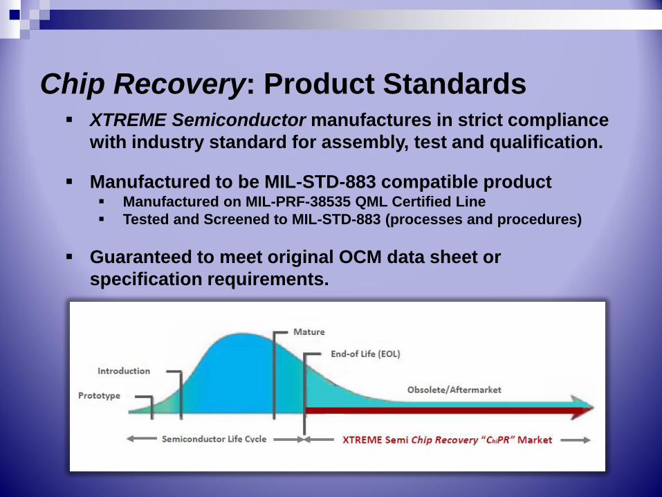
Chip Recovery: Product Standards XTREME Semiconductor manufactures in strict compliance
with industry standard for assembly, test and qualification.
Manufactured to be MIL-STD-883 compatible product Manufactured on MIL-PRF-38535 QML Certified Line
Tested and Screened to MIL-STD-883 (processes and procedures)
Guaranteed to meet original OCM data sheet or
specification requirements.
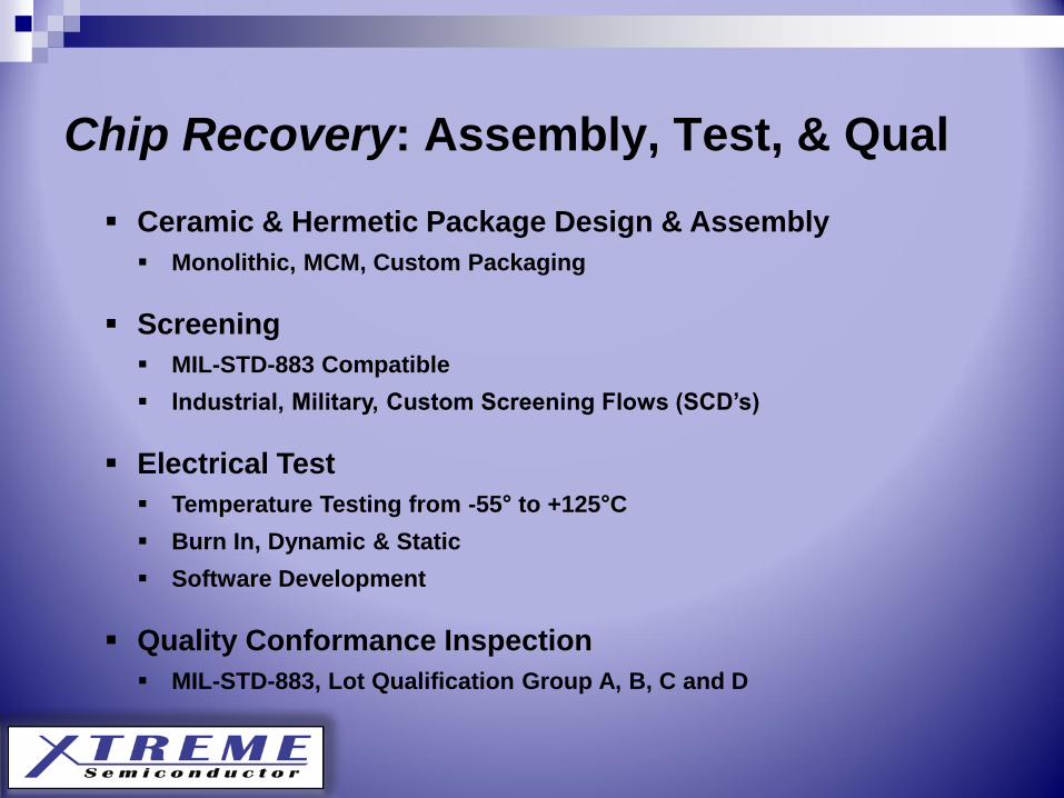
Chip Recovery: Assembly, Test, & Qual
Ceramic & Hermetic Package Design & Assembly
Monolithic, MCM, Custom Packaging
Screening
MIL-STD-883 Compatible
Industrial, Military, Custom Screening Flows (SCD’s)
Electrical Test
Temperature Testing from -55° to +125°C
Burn In, Dynamic & Static
Software Development
Quality Conformance Inspection
MIL-STD-883, Lot Qualification Group A, B, C and D

Chip Recovery “ChiPR” Product
All Chip Recovery “ChiPR” product is clearly identified;
All correspondence, including the final quote, states the
product contains extracted die;
XTREME Semiconductor works closely with the customer
to define the appropriate qualification plan based on their
application and requirements.

Successful Chip Recovery “ChiPR” Product• Solved Product Obsolescence issue for our Customer
• AD746SRC – Replacement for OP215BRC
• 79% Overall Yield Die Extraction through finished product
• Test yield attributed to commercial grade product up-
screening
Process Description QTY
Die extraction AD746JRZ, 8-pin SOIC 154
Assembly 20-pin Ceramic LCC - MIL-STD-883 M5004 Class B *149
Environmental MIL-STD-883 M5004 (CA, TC, FL and GL) 139
Pre-Test AD746 Data Sheet Electrical, +25C 122
Burn-in MIL-STD-883 M5004, Test Condition 1015, 160hrs 122
Post-Test AD746 Data Sheet Electrical, +25C 122
Final Test AD746 Data Sheet Electrical, -55, +25 and 125C 122
* 10pcs pulled out for First Article Inspection
XT746SRC-2A MILITARY CLASS B ASSEMBLY/TEST

Successful Chip Recovery “ChiPR” Product
• Solved Product Obsolescence issue for customer
• ADSP1016ASE obsoleted by Analog devices
• Yield losses attributed to commercial grade product
up-screening…..99% assembly/test yield
Process Description QTYDie extraction ADSP1016AJN, 16x16-bit CMOS Multilier *252
Assembly 68-pin Ceramic LCC - MIL-STD-883 M5004 Class B 223
Environmental Temp Cycle : MIL-STD-883 M5004, Cond. 223
Environmental Const. Accel: MIL-STD-883 M5004, Cond. 223
Environmental Fine Leak: MIL-STD-883 M5004, Cond. 223
Environmental Gross Leak: MIL-STD-883 M5004, Cond. 223
Electrical Test Test perfomred at -55 to +125C 221
Final QC Inspection, 220pcs shipped to customer 220
* 5pcs used as assembly set-up samples
* 18pcs failed M5004 Class B die visual however accepted as commercial grade product
* 5pcs used for first article inspection.
* 2pcs failed electrical test at Military temps, passed 25C testing
ADSP1016ASE-MT MILITARY CLASS B ASSEMBLY

Other Successful Die Extraction Products
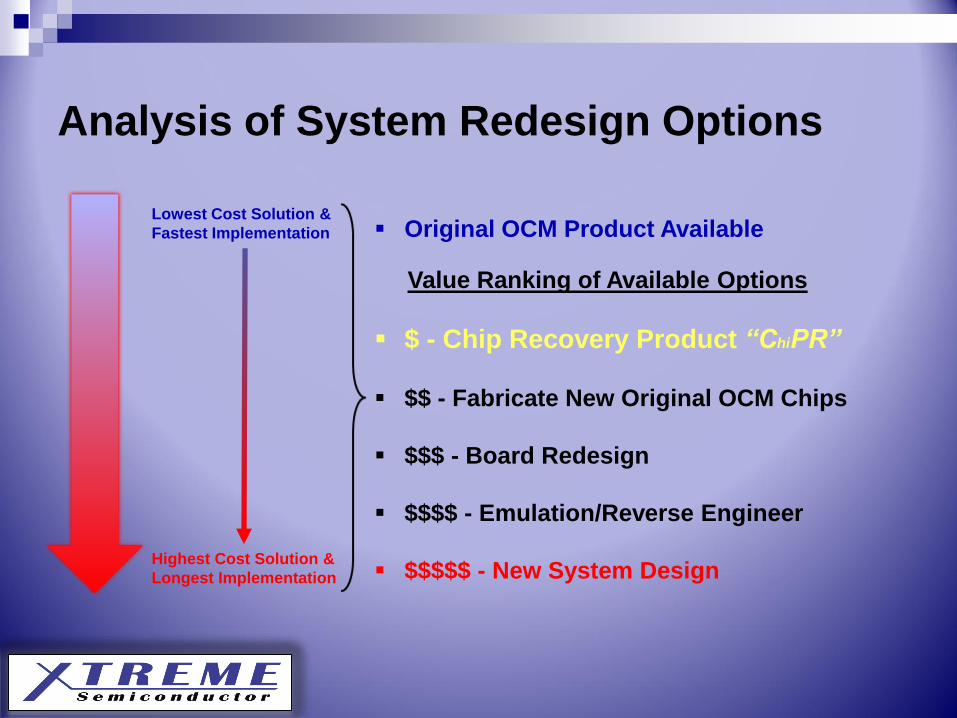
Analysis of System Redesign Options
Original OCM Product Available
Value Ranking of Available Options
$ - Chip Recovery Product “ChiPR”
$$ - Fabricate New Original OCM Chips
$$$ - Board Redesign
$$$$ - Emulation/Reverse Engineer
$$$$$ - New System Design
Lowest Cost Solution &
Fastest Implementation
Highest Cost Solution &
Longest Implementation

Chip Recovery “ChiPR”: Processes
Removes die from a package undamaged,
maintaining original electrical characteristics
Results in a “Known-Good” electrically tested
die, ready for reassembly
Die thinning may also be achieved
Can be performed on any package type
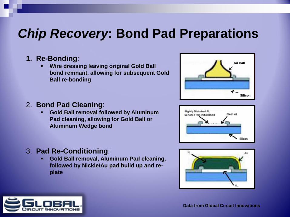
Chip Recovery: Bond Pad Preparations
1. Re-Bonding: Wire dressing leaving original Gold Ball
bond remnant, allowing for subsequent Gold
Ball re-bonding
2. Bond Pad Cleaning: Gold Ball removal followed by Aluminum
Pad cleaning, allowing for Gold Ball or
Aluminum Wedge bond
3. Pad Re-Conditioning: Gold Ball removal, Aluminum Pad cleaning,
followed by Nickle/Au pad build up and re-
plate
Au Ball
Silicon
Data from Global Circuit Innovations

Chip Recovery: Bond Pad Re-bonding
Chip Recovery Die ready for re-bonding
Data from Global Circuit Innovations

Chip Recovery: Bond Pad Re-bonding
Original Gold Ball and Aluminum Wedge
Bonds Compound Gold Ball and Aluminum
Wedge Bonds
Wire Bonding
Original Gold or Aluminum wires are mechanically removed
at the top of the original bond
Clean, uncontaminated gold or aluminum surface is used
for the new, high-adhesion wire connection
New bond formation is made to original pristine bond,
NOT a re-bond.
Data from Global Circuit Innovations
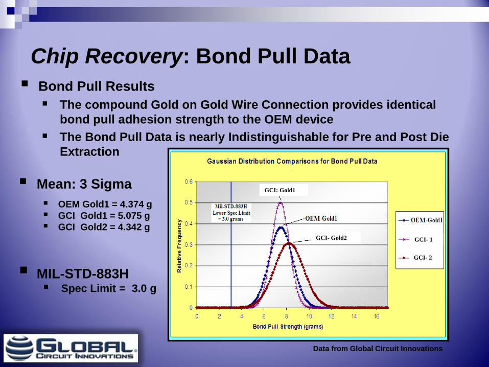
Chip Recovery: Bond Pull Data
Bond Pull Results
The compound Gold on Gold Wire Connection provides identical
bond pull adhesion strength to the OEM device
The Bond Pull Data is nearly Indistinguishable for Pre and Post Die
Extraction
Mean: 3 Sigma
OEM Gold1 = 4.374 g
GCI Gold1 = 5.075 g
GCI Gold2 = 4.342 g
MIL-STD-883H Spec Limit = 3.0 g
GCI- Gold2
GCI: Gold1
GCI- 1
GCI- 2
Data from Global Circuit Innovations

Chip Recovery: Bond Pad Cleaning
Chip Recovery Die with Remnant Bond
Wires Removed and Pads Cleaned
Data from Global Circuit Innovations

Chip Recovery: Bond Pad Cleaning
1. Original Gold Ball bond
2. After removal of Gold Ball bond
3. New bonding area ready for new Gold
Ball or Aluminum Wedge bonding
Data from Global Circuit Innovations

Chip Recovery: Bond Pad Reconditioning
Nickle/Au Metallization UBM (Under-Bump Metal) Process
Data from Global Circuit Innovations

Chip Recovery: Bond Pad ReconditioningNi/Au Metallization UBM process
Cross Section of Au
Bond and new Ni/Au PadGold Ball Bond on new
Ni/Au Pad
Data from Global Circuit Innovations

Chip Recovery: Bond Pad ReconditioningNi/Au Metallization UBM process
Reconditioned Bond Pads ready for Gold Ball or
Aluminum Wedge Bonding
Data from Global Circuit Innovations

Chip Recovery: Bond Pad ReconditioningNi/Au Metallization UBM process
Why consider our Gold Ball removal and Ni/Au Metallization
UMB process?
Eliminates MIL-STD compound bonding concerns and provides
bare die with a consistent, predictable bonding surface.
Proven to provide superior bond strength if original bonding has
not been optimized.
Conventional Bond Strength: Mean 3 SD = 4.01g
Ni/Au Metallization UBM Process: Mean 3 SD = 8.74g
The new Ni/Au bonding interface dramatically reduces Inter-
Metallic Diffusion (Kirkendall Voiding), therefore, creating a much
more robust bonding process relative to high temperature (>175C)
exposures.
Provides new metallization compatible with High Reliability and
small pitch Gold Ball bonding requirements.
Data from Global Circuit Innovations

Chip Recovery: Bond Pad ReconditioningNi/Au Metallization UBM process
Packaging Option Key
1. Standard Plastic Packaged Product
2. Die Recovery, Standard Ceramic Assembly
3. Die Recovery, High-Temp Ceramic Assembly
4. Die Recovery with Ni/Au Reconditioned bond pads,
High-Temp Ceramic Assembly
5. Die Recovery with Ni/Au Reconditioned bond pads,
Standard Ceramic Assembly
Data from Global Circuit Innovations
1
10
100
1000
10000
1 2 3 4 5
Ho
urs
Packaging Options
Hours to Failure @ 250C

Chip Recovery: Bond Remapping and
Reassembly Options
Multiple Device configurations for
the same ship can be achieved with
remapping optional bond outs. Memory Devices: Bond options for x4,
x8, x16 devices from the same chip
FPGA’s: Reconfigure to create
multiple devices from a single chip
Examples of Remapping Options• Original non-bonded pad, still not
bonded
• Original non-bonded pad, now bonded
• Previously bonded pad, now not
bonded
• Previously bonded pad, re-bonded with
new compound bond.
Data from Global Circuit Innovations

Chip Recovery “ChiPR” Product
Benefits of Chip Recovery Chip Recovery and re-assembly is an excellent solution to IC
Component Obsolescence – Solves DMSMS problems.
Die can be removed from virtually ANY plastic or ceramic package without damaging the die, while maintaining FULL functionality.
Chip Recovery allows fully functional die to be re-assembled into ANY plastic or ceramic package, MCM, or hybrid module
Die Shear and Bond Pull data are identical to or exceed original OCM product.
Allows access to original OCM die stock, while avoiding costly minimum order die or wafer purchases.
Offers a direct replacement for the original OCM product

Chip Recovery “ChiPR”
“Breathing New Life into Obsolescence”
Any Questions?
Marty Lanning
XTREME Semiconductor
Managing Partner
Office: 858-230-6961
Cell: 619-675-1808
Erick Spory
Global Circuit Innovations
President & CTO
Office: 719-573-6777 x104
Cell: 719-649-0947