Chieh Chang
11
Chieh Chang Chieh Chang EE 235 – Presentation I EE 235 – Presentation I March 20, March 20, 2007 2007 Nanoimprint Lithography Nanoimprint Lithography for Hybrid Plastic for Hybrid Plastic Electronics Electronics Michael C. McAlpine, Robin S. Friedman, and Charles M. Lieber Michael C. McAlpine, Robin S. Friedman, and Charles M. Lieber Harvard UniVersity Harvard UniVersity
-
Upload
luke-schwartz -
Category
Documents
-
view
42 -
download
0
description
Nanoimprint Lithography for Hybrid Plastic Electronics Michael C. McAlpine, Robin S. Friedman, and Charles M. Lieber Harvard UniVersity. Chieh Chang. EE 235 – Presentation IMarch 20, 2007. Introduction. Efficient fabrication of integrated circuits Reliable High-throughput processing - PowerPoint PPT Presentation
Transcript of Chieh Chang
Chieh ChangChieh ChangEE 235 – Presentation IEE 235 – Presentation I March 20, March 20, 20072007
Nanoimprint Lithography Nanoimprint Lithography for Hybrid Plastic for Hybrid Plastic ElectronicsElectronicsMichael C. McAlpine, Robin S. Friedman, and Charles M. Michael C. McAlpine, Robin S. Friedman, and Charles M. LieberLieberHarvard UniVersityHarvard UniVersity
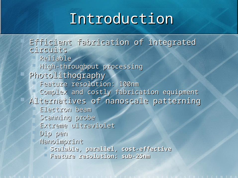
IntroductionIntroduction Efficient fabrication of integrated circuitsEfficient fabrication of integrated circuits
Reliable Reliable High-throughput processingHigh-throughput processing
PhotolithographyPhotolithography Feature resolution: 100nmFeature resolution: 100nm Complex and costly fabrication equipmentComplex and costly fabrication equipment
Alternatives of nanoscale patterningAlternatives of nanoscale patterning Electron beamElectron beam Scanning probeScanning probe Extreme ultravioletExtreme ultraviolet Dip penDip pen NanoimprintNanoimprint
Scalable, parallel, cost-effectiveScalable, parallel, cost-effective Feature resolution: sub-25nmFeature resolution: sub-25nm
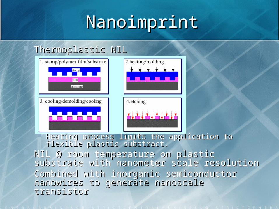
NanoimprintNanoimprint Thermoplastic NILThermoplastic NIL
Heating process limits the application to flexible Heating process limits the application to flexible plastic substract.plastic substract.
NIL @ room temperature on plastic substrate NIL @ room temperature on plastic substrate with nanometer scale resolutionwith nanometer scale resolution
Combined with inorganic semiconductor Combined with inorganic semiconductor nanowires to generate nanoscale transistor nanowires to generate nanoscale transistor
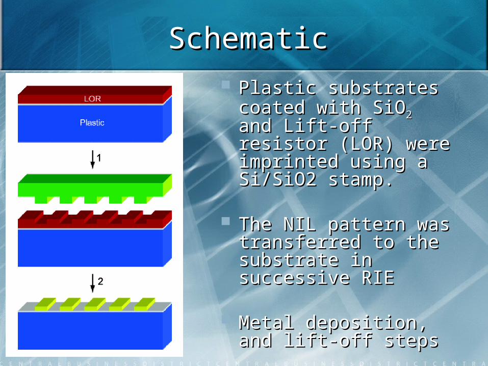
SchematicSchematic Plastic substrates Plastic substrates
coated with SiOcoated with SiO22 and and Lift-off resistor (LOR) Lift-off resistor (LOR) were imprinted using were imprinted using a Si/SiO2 stamp. a Si/SiO2 stamp.
The NIL pattern was The NIL pattern was transferred to the transferred to the substrate in substrate in successive RIEsuccessive RIE
Metal deposition, and Metal deposition, and lift-off stepslift-off steps
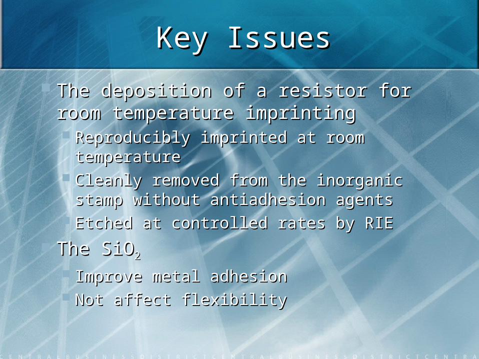
Key IssuesKey Issues
The deposition of a resistor for room The deposition of a resistor for room temperature imprintingtemperature imprinting Reproducibly imprinted at room Reproducibly imprinted at room
temperaturetemperature Cleanly removed from the inorganic stamp Cleanly removed from the inorganic stamp
without antiadhesion agentswithout antiadhesion agents Etched at controlled rates by RIEEtched at controlled rates by RIE
The SiOThe SiO22
Improve metal adhesionImprove metal adhesion Not affect flexibilityNot affect flexibility
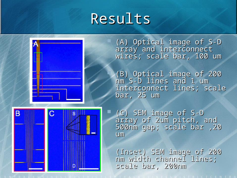
ResultsResults (A) Optical image of S-D (A) Optical image of S-D
array and interconnect array and interconnect wires; scale bar, 100 umwires; scale bar, 100 um
(B) Optical image of 200 nm (B) Optical image of 200 nm S-D lines and 1 um S-D lines and 1 um interconnect lines; scale interconnect lines; scale bar, 25 umbar, 25 um
(C) SEM image of S-D array (C) SEM image of S-D array of 2um pitch, and 500nm of 2um pitch, and 500nm gap; scale bar ,20 umgap; scale bar ,20 um
(Inset) SEM image of 200 (Inset) SEM image of 200 nm width channel lines; nm width channel lines; scale bar, 200nmscale bar, 200nm
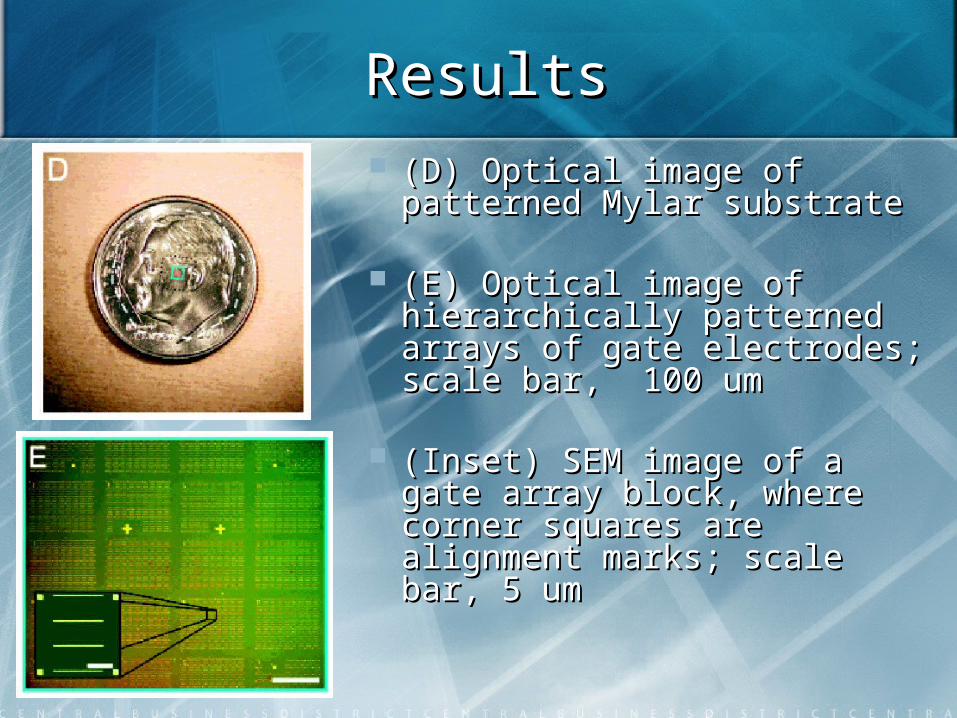
ResultsResults (D) Optical image of (D) Optical image of
patterned Mylar substrate patterned Mylar substrate
(E) Optical image of (E) Optical image of hierarchically patterned hierarchically patterned arrays of gate electrodes; arrays of gate electrodes; scale bar, 100 umscale bar, 100 um
(Inset) SEM image of a gate (Inset) SEM image of a gate array block, where corner array block, where corner squares are alignment squares are alignment marks; scale bar, 5 ummarks; scale bar, 5 um
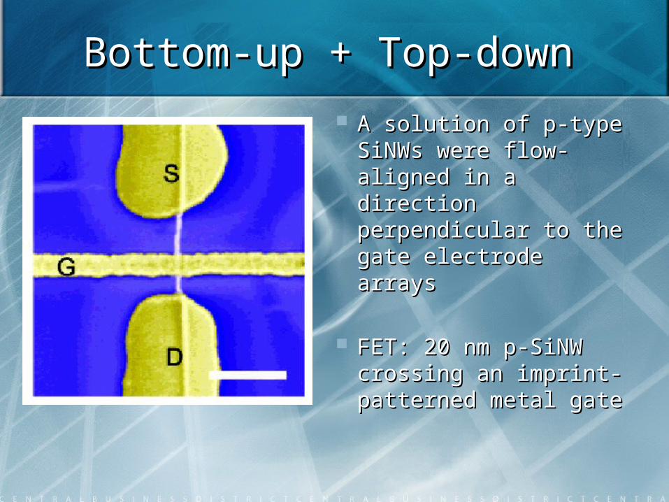
Bottom-up + Top-down Bottom-up + Top-down
A solution of p-type A solution of p-type SiNWs were flow-SiNWs were flow-aligned in a direction aligned in a direction perpendicular to the perpendicular to the gate electrode arraysgate electrode arrays
FET: 20 nm p-SiNW FET: 20 nm p-SiNW crossing an imprint-crossing an imprint-patterned metal gatepatterned metal gate
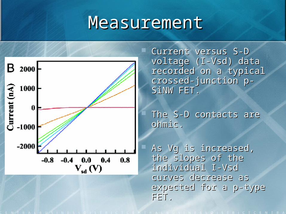
MeasurementMeasurement Current versus S-D Current versus S-D
voltage (I-Vsd) data voltage (I-Vsd) data recorded on a typical recorded on a typical crossed-junction p-SiNW crossed-junction p-SiNW FET.FET.
The S-D contacts are The S-D contacts are ohmic. ohmic.
As Vg is increased, the As Vg is increased, the slopes of the individual I-slopes of the individual I-Vsd curves decrease as Vsd curves decrease as expected for a p-type expected for a p-type FET.FET.
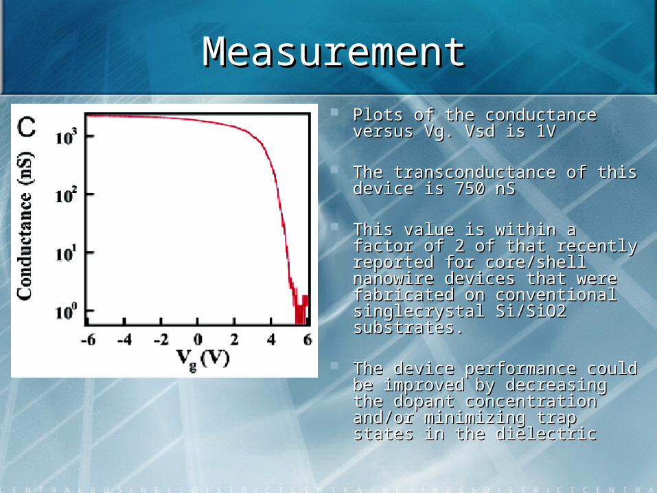
MeasurementMeasurement Plots of the conductance Plots of the conductance
versus Vg. Vsd is 1Vversus Vg. Vsd is 1V
The transconductance of this The transconductance of this device is 750 nSdevice is 750 nS
This value is within a factor of This value is within a factor of 2 of that recently reported for 2 of that recently reported for core/shell nanowire devices core/shell nanowire devices that were fabricated on that were fabricated on conventional singlecrystal conventional singlecrystal Si/SiO2 substrates.Si/SiO2 substrates.
The device performance could The device performance could be improved by decreasing be improved by decreasing the dopant concentration the dopant concentration and/or minimizing trap states and/or minimizing trap states in the dielectricin the dielectric
SummarySummary This paper has demonstrated NIL of nanometer through This paper has demonstrated NIL of nanometer through
millimeter-scale features on flexible plastic substrates millimeter-scale features on flexible plastic substrates over large areas at room temperature. over large areas at room temperature.
The ambient temperature NIL patterning technique has The ambient temperature NIL patterning technique has been shown to produce uniform features in a parallel and been shown to produce uniform features in a parallel and repeatable mannerrepeatable manner
Moreover, NIL has been combined with bottom up Moreover, NIL has been combined with bottom up assembly to fabricate SiNW FETs on flexible plastic assembly to fabricate SiNW FETs on flexible plastic substrates with device performances similar to nanowire substrates with device performances similar to nanowire FETs fabricated on conventional single-crystal substrates. FETs fabricated on conventional single-crystal substrates.
The development of simple and reproducible high-The development of simple and reproducible high-resolution patterning of plastics using NIL combined with resolution patterning of plastics using NIL combined with the versatile function of nanowire building blocks could the versatile function of nanowire building blocks could open up exciting opportunities over many length scales open up exciting opportunities over many length scales for plastic electronics and photonics.for plastic electronics and photonics.