Chemical Bath Deposition Of Group Ii-vi Semiconductor Thin ...
209
University of Central Florida University of Central Florida STARS STARS Electronic Theses and Dissertations, 2004-2019 2009 Chemical Bath Deposition Of Group Ii-vi Semiconductor Thin Chemical Bath Deposition Of Group Ii-vi Semiconductor Thin Films For Solar Cells Applications Films For Solar Cells Applications Hani Khallaf University of Central Florida Part of the Physics Commons Find similar works at: https://stars.library.ucf.edu/etd University of Central Florida Libraries http://library.ucf.edu This Doctoral Dissertation (Open Access) is brought to you for free and open access by STARS. It has been accepted for inclusion in Electronic Theses and Dissertations, 2004-2019 by an authorized administrator of STARS. For more information, please contact [email protected]. STARS Citation STARS Citation Khallaf, Hani, "Chemical Bath Deposition Of Group Ii-vi Semiconductor Thin Films For Solar Cells Applications" (2009). Electronic Theses and Dissertations, 2004-2019. 3941. https://stars.library.ucf.edu/etd/3941
Transcript of Chemical Bath Deposition Of Group Ii-vi Semiconductor Thin ...

University of Central Florida University of Central Florida
STARS STARS
Electronic Theses and Dissertations, 2004-2019
2009
Chemical Bath Deposition Of Group Ii-vi Semiconductor Thin Chemical Bath Deposition Of Group Ii-vi Semiconductor Thin
Films For Solar Cells Applications Films For Solar Cells Applications
Hani Khallaf University of Central Florida
Part of the Physics Commons
Find similar works at: https://stars.library.ucf.edu/etd
University of Central Florida Libraries http://library.ucf.edu
This Doctoral Dissertation (Open Access) is brought to you for free and open access by STARS. It has been accepted
for inclusion in Electronic Theses and Dissertations, 2004-2019 by an authorized administrator of STARS. For more
information, please contact [email protected].
STARS Citation STARS Citation Khallaf, Hani, "Chemical Bath Deposition Of Group Ii-vi Semiconductor Thin Films For Solar Cells Applications" (2009). Electronic Theses and Dissertations, 2004-2019. 3941. https://stars.library.ucf.edu/etd/3941

CHEMICAL BATH DEPOSITION OF GROUP II-VI SEMICONDUCTOR THIN FILMS FOR SOLAR CELLS APPLICATIONS
by
HANI M. KHALLAF
B.S. El-Minia University, 1998 M.S. University of Central Florida, 2005
A dissertation submitted in partial fulfillment of the requirements
for the degree of Doctor of Philosophy in the Department of Physics
in the College of Sciences at the University of Central Florida
Orlando, Florida
Fall Term 2009
Major Professor: Lee Chow

ii
© 2009 Hani M. Khallaf

iii
ABSTRACT
Chemical bath deposition (CBD) is the analog in liquid phase of the well-known
chemical vapor deposition technique in the vapor phase. In CBD, deposition of thin films
takes place from aqueous solutions at low temperatures by a chemical reaction between
dissolved precursors, with the help of a complexing agent. Among all techniques used to
grow Group II-VI semiconductors, CBD has the advantage of being a simple, low
temperature, and inexpensive large-area deposition technique. So far, its contribution in
thin film solar cells industry has been mainly limited to growing n-type CdS and/or ZnS
window layers for CdTe-based and CIGS-based solar cells.
In this work we first optimize the CBD process of CdS using nitrilotriacetic acid
and hydrazine as complexing agents as an alternative to ammonia. We then study the
effect of the cadmium precursor on the optical/electrical properties, as well as crystal
structure, morphology, and composition of CBD-CdS films. A better understanding of
the CBD process of CdS as a whole has been achieved and high quality CBD-CdS films
have been obtained.
Next, we investigate in-situ doping of CBD-CdS with group III elements, such as
B, Al, In, and Ga. The objective is to show that CBD is capable of not only growing CdS
but also of doping it to reduce its resistivity and, as a result, facilitate its use in solar cells
as well as other optoelectronic device fabrication. A four orders of magnitude drop of
film resistivity has been achieved without a significant change in film bandgap, structure,
or morphology.

iv
Finally, we test the possibility of using CBD to grow transparent conducting
oxide (TCO) films, such as Al-doped ZnO films and cadmium stannate films. First, we
study CBD of ZnO and later in-situ doping of ZnO using Al. High quality ZnO thin films
have been grown using CBD with the help of four different complexing agents. Post
heat treatment in argon ambient helped reduce resistivity of CBD-ZnO undoped films to
~ 10-1 Ω-cm. In-situ doping of such films using Al shows promising results. Such films
could be an alternative to indium tin oxide (ITO) layers that are commonly used as TCO
layers for solar cells. Another approach is to use CBD to grow CdO and SnO2 thin films,
with the goal of obtaining Cd2SnO4 by later annealing of these two layers. Cadmium
stannate is another TCO candidate that could replace ITO in the near future. We have
succeeded in growing CBD-CdO thin films using three different complexing agents.
Undoped CBD-CdO films with a resistivity as low as 1.01 x10⁻² Ω-cm and a carrier
density as high as 2.59 x 1020 cm-3 have been obtained. SnO2 films have been
successfully grown using CBD. Fabrication of Cadmium stannate thin films using CBD
is investigated.
In summary, our objective to expand the use of CBD beyond just growing CdS
and ZnS, and to test the possibility of using it for in-situ doping of group II-VI
semiconductors as well as TCO layers fabrication proved to be successful. We believe
that this may have a significant impact on solar cells as well as other optoelectronic
devices fabrication industry, due to the simplicity and the cost-effectiveness of CBD.

v
To my parents, my sister, and my brother for their endless support, encouragement, and
unconditional love

vi
ACKNOWLEDGMENTS
I am deeply grateful to Dr. Lee Chow, my adviser, for his kind help, support,
patience, and guidance throughout this work. I am really thankful to my dissertation
committee members; Dr. Helge Heinrich, Dr. Juin J. Liou, Dr. Eduardo Mucciolo, and
Dr. Alfons Schulte for their help and support. I am most indebted to Dr. Guangyu Chai
of Planar Energy Devices Corporation, Orlando, FL, as well as Dr. Oleg Lupan of the
department of microelectronics and semiconductor devices, technical university of
Moldova, and Mr. Chia-ta Chen of the institute of electro-optical engineering, Chang
Gung university, Taiwan, for their kind help and guidance that made this work possible.
I am also grateful to Mr. Kirk Scammon of the advanced materials processing and
analysis center (AMPAC), university of central Florida, for his help with the XPS and
RBS measurements, Mr. Sanghoon Park and Mr. Firoze Haque of the department of
physics, university of central Florida for their help with the micro-Raman, FTIR, and
AFM measurements, as well as Dr. Aravinda Kar and his group, especially Dr. Sachin
Bet and Mr. G. Lim, of the college of optics and photonics, university of central Florida,
for their help with the Hall measurements. I am really thankful to John Wiley & Sons,
Inc. for granting me permission to reprint excerpts from Refs. [ 15, 17]. Permission to
reprint excerpts from Ref. [ 9] has been granted by Springer. Permission to reprint
excerpts from Ref. [ 14] has been granted by Taylor & Francis Group LLC through
www.copyright.com.

vii
TABLE OF CONTENTS
LIST OF FIGURES ........................................................................................................... xi
LIST OF TABLES ........................................................................................................... xix
CHAPTER I: INTRODUCTION ........................................................................................ 1
1.1 Group II-VI Semiconductors .................................................................................... 1
1.1.1 Crystal Structure ................................................................................................ 1
1.1.2 Chemical Binding .............................................................................................. 4
1.1.3 Phonon Frequency ............................................................................................. 6
1.1.4 Elastic Properties ............................................................................................... 6
1.1.5 Thermal Properties ............................................................................................. 8
1.1.6 Optical Properties ............................................................................................... 9
1.1.7 Electrical Properties ......................................................................................... 10
1.2 Chemical Bath Deposition ...................................................................................... 12
1.2.1 Chemical Bath Deposition of CdS ................................................................... 14
1.3 Research Objectives ................................................................................................ 19
CHAPTER II: A NEW APPROACH TOWARDS OPTIMIZATION OF CBD-CdS ..... 21
2.1 Optimization of CBD-CdS Thin Films Using Nitrilotriacetic Acid as a Complexing
Agent ............................................................................................................................. 21
2.1.1 Introduction ...................................................................................................... 21
2.1.2 Experimental Details ........................................................................................ 23
2.1.3 Results and Discussion .................................................................................... 25
2.1.4 Conclusion ....................................................................................................... 41

viii
2.2 Characterization of CdS Thin Films Grown by Chemical Bath Deposition Using
Four Different Cadmium Sources ................................................................................. 43
2.2.1 Introduction ...................................................................................................... 43
2.2.2 Experimental Details ........................................................................................ 45
2.2.3 Results and Discussion .................................................................................... 46
2.2.4 Conclusion ....................................................................................................... 57
CHAPTER III: IN–SITU DOPING OF CBD–CdS USING GROUP III ELEMENTS ... 59
3.1 Investigation of Aluminum and Indium In-situ Doping of Chemical Bath Deposited
CdS Thin Films ............................................................................................................. 59
3.1.1 Introduction ...................................................................................................... 59
3.1.2 Experimental Details ........................................................................................ 61
3.1.3 Results and Discussion .................................................................................... 62
3.1.4 Conclusion ....................................................................................................... 82
3.2 Boron In-Situ Doping of Chemical Bath Deposited CdS Thin Films ..................... 83
3.2.1 Introduction ...................................................................................................... 83
3.2.2 Experimental Details ........................................................................................ 84
3.2.3 Results and Discussion .................................................................................... 84
3.2.4 Conclusion ....................................................................................................... 97
3.3 Characterization of Gallium-Doped CdS Thin Films Grown by Chemical Bath
Deposition ..................................................................................................................... 99
3.3.1 Introduction ...................................................................................................... 99
3.3.2 Experimental Details ...................................................................................... 100
3.3.3 Results and Discussion .................................................................................. 101

ix
3.3.4 Conclusion ..................................................................................................... 114
CHAPTER VI: CHEMICAL BATH DEPOSITION OF TRANSPARENT
CONDUCTING OXIDES .............................................................................................. 116
4.1 Investigation of Chemical Bath Deposition of ZnO Thin Films Using Six Different
Complexing Agents .................................................................................................... 116
4.1.1 Introduction .................................................................................................... 116
4.1.2 Experimental Details ...................................................................................... 118
4.1.3 Results and Discussion .................................................................................. 119
4.1.4 Conclusion ..................................................................................................... 133
4.2 Investigation of Chemical Bath Deposition of CdO Thin Films Using Three
Different Complexing Agents ..................................................................................... 136
4.2.1 Introduction .................................................................................................... 136
4.2.2 Experimental Details ...................................................................................... 137
4.2.3 Results and Discussion .................................................................................. 138
4.2.4 Conclusion ..................................................................................................... 151
4.3 Investigation of Chemical Bath Deposition of SnO2 and Cd2SnO4 Thin Films ... 153
4.3.1 Introduction .................................................................................................... 153
4.3.2 Experimental Details ...................................................................................... 155
4.3.3 Results and Discussion .................................................................................. 156
4.3.4 Conclusion ..................................................................................................... 164
CONCLUSION ............................................................................................................... 166
APPENDIX A: COPYRIGHTS PERMISSION OF REFERENCE [ 15] ....................... 169
APPENDIX B: COPYRIGHTS PERMISSION OF REFERENCE [ 17] ....................... 171

x
REFERENCES: .............................................................................................................. 173

xi
LIST OF FIGURES
Fig. 1 Zincblende structure of CdS [ 11] ............................................................................. 3
Fig. 2 Wurtzite structure of ZnO [ 11] ................................................................................. 3
Fig. 3 Melting point Tm versus lattice constant a for some group II-VI semiconductor
compounds .......................................................................................................................... 7
Fig. 4 Graphical solution of Eq. 13 (hydroxide line) and Eq. 16 (complex line) for CBD
of Cd-NH3 system ............................................................................................................. 18
Fig. 5 Film thickness/ Eg dependence on (a) [NTA]/[Cd] ratio, (b) KOH concentration
(Films were deposited on SnO2 coated soda lime glass) .................................................. 27
Fig. 6 Transmission spectra of films deposited at different (a) [NTA]/[Cd] ratios, (b)
KOH concentration (Films were deposited on SnO2 coated soda lime glass) .................. 29
Fig. 7 Film thickness/ Eg dependence on (a) [NTA]/[Cd] ratio, (b) KOH concentration
(Films were deposited on SnO2 coated soda lime glass) .................................................. 33
Fig. 8 Transmission spectra of films deposited at different (a) [NTA]/[Cd] ratios, (b)
KOH concentration (Films were deposited on SnO2 coated soda lime glass) .................. 34
Fig. 9 Transmission spectra (a) and Eg (b) of CdS films deposited on quartz using two
different Cd sources .......................................................................................................... 38
Fig. 10 SEM micrographs of CdS films deposited on quartz using two different Cd
sources............................................................................................................................... 39
Fig. 11 XRD patterns of CdS films deposited on quartz using two different Cd sources 39
Fig. 12 RBS spectrum of CdS films deposited on quartz using two different Cd sources 40

xii
Fig. 13 Specular transmission spectra of CdS films grown using four different Cd
sources; CdSO4 (0.18 μm), Cd(CH3COO)2 (0.19 μm), CdCl2 (0.20 μm), and CdI2 (0.185
μm) .................................................................................................................................... 49
Fig. 14 SEM micrograph of CdS films grown using four different Cd sources ............... 49
Fig. 15 Specular reflectance of CdCl2-based film (0.20 μm) and CdSO4-based film (0.18
μm) .................................................................................................................................... 50
Fig. 16 Optical band gap calculations of CdS films grown using four different Cd sources
........................................................................................................................................... 50
Fig. 17 XRD pattern of CdS films grown using four different Cd sources ...................... 51
Fig. 18 RBS spectrum and RUMP simulation of CdS films grown using four different Cd
sources............................................................................................................................... 56
Fig. 19 Specular transmittance and reflectance spectra of Al-doped CdS films grown at
different [Al] / [Cd] ratios (R denotes [Al] / [Cd] ratio & R = 0.000 refers to undoped
film)................................................................................................................................... 63
Fig. 20 Optical bandgap calculations of Al-doped CdS films grown at different [Al] /
[Cd] ratios (R denotes [Al] / [Cd] ratio & R = 0.000 refers to undoped film) .................. 63
Fig. 21 Optical bandgap of Al-doped CdS films as a function of [Al] / [Cd] ratio .......... 65
Fig. 22 XRD pattern of Al-doped CdS films grown at different [Al] / [Cd] ratios (R
denotes [Al] / [Cd] ratio & R = 0.000 refers to undoped film) ......................................... 65
Fig. 23 Average (111) interplanar distance d(111) and relative intensity I / Io of the (111)
peak with respect to that of undoped film as a function of [Al] / [Cd] ratio .................... 67
Fig. 24 Grain size dependence on [Al] / [Cd] ratio ........................................................... 67
Fig. 25 Carrier concentration dependence on [Al] / [Cd] ratio ......................................... 70

xiii
Fig. 26 Dark resistivity as a function of [Al] / [Cd] ratio ................................................. 70
Fig. 27 Variation of Hall mobility with [Al] / [Cd] ratio .................................................. 71
Fig. 28 Raman spectra of Al-doped films grown at different [Al] / [Cd] ratio (R denotes
[Al] /[Cd] ratio) ................................................................................................................. 71
Fig. 29 Deconvolution of the 303 cm-1 Raman peak of film grown at [Al] / [Cd] ratio of
0.018 into three peaks using Gaussian fit ......................................................................... 72
Fig. 30 Phase transition of undoped film due to annealing as detected by Raman; (a)
Substrate, (b) As-grown undoped CdS film, and (c) Annealed undoped CdS film .......... 72
Fig. 31 Peak position and FWHM as a function of [Al] / [Cd] ratio; (a) E2 peak of
hexagonal CdS, (b) Shifted TO peak of cubic CdS, and (c) Cubic 1LO or hexagonal
A1(LO) / E1 (LO) peak ...................................................................................................... 76
Fig. 32 XPS multiplex spectra of undoped CdS film, Al-doped film grown at [Al] / [Cd]
ratio of 0.036 and 0.18; (a) S 2p peak, and (b) Cd 3d peak .............................................. 77
Fig. 33 SEM micrographs of (a) CdS undoped film, and (b) Al-doped film grown at [Al] /
[Cd] ratio of 0.036............................................................................................................. 79
Fig. 34 Specular transmittance and reflectance spectra of films grown at [In] / [Cd] ratios
of 0.009 and 0.018 ............................................................................................................ 79
Fig. 35 Optical bandgap calculations of films grown at [In] / [Cd] ratios of 0.009 and
0.018.................................................................................................................................. 80
Fig. 36 XRD pattern of film grown at [In] / [Cd] ratio of 0.018 ...................................... 80
Fig. 37 Specular transmittance and reflectance spectra of B-doped CdS films grown at
different [B] / [Cd] ratio, R (R = 0.0 is assigned to the undoped film) ............................ 86

xiv
Fig. 38 Optical bandgap calculations of B-doped CdS films grown at different [B] / [Cd]
ratio, R............................................................................................................................... 86
Fig. 39 Optical bandgap of B-doped CdS films as a function of [B] / [Cd] ratio ............. 87
Fig. 40 XRD pattern of B-doped CdS films grown at different [B] / [Cd] ratio, R .......... 87
Fig. 41 Average (111) / (0002) interplanar distance d(111) / d(0002) as a function of [B] /
[Cd] ratio ........................................................................................................................... 89
Fig. 42 High-resolution TEM of film grown at a [B] / [Cd] ratio of 5.1 x 10⁻² ................ 89
Fig. 43 TEM diffraction pattern of film grown at a [B] / [Cd] ratio of 5.1 x 10⁻² ............ 90
Fig. 44 Carrier concentration (C.C.) dependence on [B] / [Cd] ratio ............................... 90
Fig. 45 Dark resistivity as a function of [B] / [Cd] ratio ................................................... 93
Fig. 46 Variation of Hall mobility (μ) with [B] / [Cd] ratio ............................................. 93
Fig. 47 Raman spectra of B-doped films grown at different [B] / [Cd] ratio, R ............... 94
Fig. 48 Deconvolution of the 303 cm-1 Raman peak of film grown at [B] / [Cd] ratio of
5.1 x 10⁻² into three peaks using Gaussian fitting ............................................................. 94
Fig. 49 Peak position and FWHM as a function of [B] / [Cd] ratio; (a) E2 peak of
hexagonal CdS, (b) Shifted TO peak of cubic CdS, and (c) Cubic 1LO or hexagonal
A1(LO) / E1 (LO) peak ...................................................................................................... 95
Fig. 50 XPS multiplex spectra of undoped CdS film, and B-doped film grown at [B] /
[Cd] ratio of 1.7 x 10⁻²; (a) S 2p peak, and (b) Cd 3d peak .............................................. 95
Fig. 51 SEM micrographs of (a) CdS undoped film, and (b) B-doped film grown at [B] /
[Cd] ratio of 1.7 x 10⁻² ...................................................................................................... 96

xv
Fig. 52 Specular transmittance and reflectance spectra of Ga-doped CdS films grown at
different [Ga] / [Cd] ratios (R denotes [Ga] / [Cd] ratio & R = 0.0 refers to undoped film)
......................................................................................................................................... 102
Fig. 53 Optical bandgap calculations of Ga-doped CdS films grown at different [Ga] /
[Cd] ratios (R denotes [Ga] / [Cd] ratio & R = 0.0 refers to undoped film) ................... 102
Fig. 54 Optical bandgap of Ga-doped CdS films as a function of [Ga] / [Cd] ratio ....... 103
Fig. 55 XRD pattern of Ga-doped CdS films grown at different [Ga] / [Cd] ratios (R
denotes [Ga] / [Cd] ratio & R = 0.0 refers to undoped film) .......................................... 103
Fig. 56 Average (111) interplanar distance d(111) as a function of [Ga] / [Cd] ratio ....... 106
Fig. 57 Grain size dependence on [Ga] / [Cd] ratio ........................................................ 106
Fig. 58 Carrier concentration dependence on [Ga] / [Cd] ratio ...................................... 108
Fig. 59 Dark resistivity as a function of [Ga] / [Cd] ratio............................................... 108
Fig. 60 Variation of Hall mobility with [Ga] / [Cd] ratio ............................................... 109
Fig. 61 Raman spectra of Ga-doped films grown at different [Ga] / [Cd] ratio (R denotes
[Ga] / [Cd] ratio) ............................................................................................................. 109
Fig. 62 Deconvolution of the 303 cm-1 Raman peak of film grown at [Ga] / [Cd] ratio of
6.8 x 10⁻² into three peaks using Gaussian fit ................................................................. 111
Fig. 63 Peak position and FWHM as a function of [Ga] / [Cd] ratio; (a) E2 peak of
hexagonal CdS, (b) Shifted TO peak of cubic CdS, (c) Cubic 1LO or hexagonal A1(LO) /
E1 (LO) peak ................................................................................................................... 111
Fig. 64 XPS multiplex spectra of undoped CdS film, and Ga-doped film grown at [Ga] /
[Cd] ratio of 5.1 x 10⁻²; (a) S 2p peak, (b) Cd 3d peak ................................................... 113

xvi
Fig. 65 SEM micrographs of (a) CdS undoped film, (b) Ga-doped film grown at [Ga] /
[Cd] ratio of 1.7 x 10⁻² .................................................................................................... 113
Fig. 66 Specular transmittance of as-grown ZnO films deposited using six different
complexing agents .......................................................................................................... 120
Fig. 67 SEM micrographs of (a) as-grown EA-based film, (b) as-grown MA-based film,
and (c) annealed MA-based film ..................................................................................... 122
Fig. 68 Specular transmittance and reflectance of NH3, N2H4, MA and TEA-based
annealed films ................................................................................................................. 123
Fig. 69 Optical band gap calculations of as-grown and annealed N2H4-based film ....... 123
Fig. 70 XRD pattern of (a) as-grown TEA-based film and (b) annealed TEA-based film
......................................................................................................................................... 125
Fig. 71 Raman spectra of as-grown and annealed MA-based film ................................. 125
Fig. 72 RBS spectrum and RUMP simulation of annealed N2H4-based film ................. 128
Fig. 73 FTIR absorbance spectrum of as-grown MA-based film ................................... 128
Fig. 74 (a) XPS multiplex spectra of O 1s of as-grown and annealed TEA-based film, (b)
XPS multiplex spectra of Zn 2p3/2 of as-grown and annealed TEA-based film, and (c)
deconvolution of the O 1s peak of annealed TEA-based film ........................................ 129
Fig. 75 (a) HRTEM and TEM diffraction pattern (inset) of annealed NH3-based ZnO
film, and (b) Fourier-filtered HRTEM of annealed NH3-based ZnO film (low boundary is
glass substrate) ................................................................................................................ 132
Fig. 76 Specular transmittance of as-grown films deposited using three different
complexing agents .......................................................................................................... 139
Fig. 77 XRD pattern of as-grown EA-based film ........................................................... 139

xvii
Fig. 78 XRD pattern of as-grown MA-based film .......................................................... 140
Fig. 79 XRD pattern of annealed EA-based film ............................................................ 140
Fig. 80 Specular transmittance and reflectance of as-grown and annealed EA-based film
......................................................................................................................................... 142
Fig. 81 Optical band gap calculations of as-grown and annealed EA-based film .......... 142
Fig. 82 FTIR absorbance spectrum of (a) as-grown EA-based film, (b) annealed EA-
based film, and (c) as-grown MA-based film ................................................................. 143
Fig. 83 RBS spectrum and RUMP simulation of as-grown EA-based film ................... 143
Fig. 84 RBS spectrum and RUMP simulation of annealed MA-based film ................... 145
Fig. 85 XPS multiplex spectra of Cd 3d of as-grown and annealed EA-based film ....... 145
Fig. 86 Deconvolution of the Cd 3d peaks of as-grown EA-based film ......................... 146
Fig. 87 XPS multiplex spectra of O 1s of as-grown and annealed EA-based film ......... 146
Fig. 88 Deconvolution of the O 1s peak of as-grown EA-based film ............................. 148
Fig. 89 HRTEM and TEM diffraction pattern (inset) of annealed EA-based CdO film 148
Fig. 90 SEM micrographs of (a) annealed MA-based film, (b) annealed EA-based film,
and (c) annealed NH3-based film .................................................................................... 149
Fig. 91 Specular transmittance of as-grown and annealed SnO2 films and CdO+SnO2
films annealed at 500 °C and 700 °C .............................................................................. 157
Fig. 92 Optical band gap calculations of annealed SnO2 films and CdO+SnO2 films
annealed at 500 °C and 700 °C ....................................................................................... 157
Fig. 93 XRD pattern of annealed SnO2 film ................................................................... 158
Fig. 94 RBS spectrum and RUMP simulation of annealed SnO2 film ........................... 158
Fig. 95 XPS multiplex spectra of Sn 3d of annealed SnO2 film ..................................... 160

xviii
Fig. 96 XPS multiplex spectra of O 1s of annealed SnO2 film ....................................... 160
Fig. 97 2-D and 3-D AFM images of as-grown SnO2 film ............................................. 161
Fig. 98 2-D and 3-D AFM images of annealed SnO2 film ............................................. 162
Fig. 99 HRTEM and TEM diffraction pattern (inset) of annealed SnO2 film ................ 163

xix
LIST OF TABLES
Table 1 Ground state electronic configuration (GSEC) of some group II and group VI
elements .............................................................................................................................. 2
Table 2 Crystal structure, lattice parameters a, c, (c/a), bond length d, and bond ratioγ of
group II-VI semiconductors (all dimensions are in Å) [ 14] ............................................... 4
Table 3 Some physical properties of group II-VI semiconductors [ 9] ............................... 5
Table 4 Long-wavelength optical phonon frequencies (cm-1) for some group II-VI
semiconductors at 300 K [ 15] ............................................................................................. 8
Table 5 Bulk modulus B (1011 dyn/cm2), shear modulus Cs (1011 dyn/cm2), linear
compressibility Co (10-13 cm2/dyn), and microhardness H (GPa) for group II-VI
semiconductors at 300 K [ 15] ............................................................................................. 8
Table 6 Specific heat Cp, Debye temperature θD, thermal expansion coefficient αth, and
thermal conductivity K for group II-VI semiconductors at 300 K [ 15] .............................. 9
Table 7 Temperature coefficient of bandgap energy α, free exciton binding (E1) and
photoluminescence PL (X) transition energies for group II-VI semiconductors [ 14] ...... 10
Table 8 Refractive indices, static and high-frequency dielectric constants, εS and ε∞, of
group II-VI semiconductors [ 15, 16] ................................................................................ 10
Table 9 Electron and hole mobility and effective mass for some group II-VI
semiconductors at 300 K [ 16, 17] ..................................................................................... 11
Table 10 Thickness and Eg of optimized CdSO4 – based CdS films ................................ 31
Table 11 Thickness and Eg of optimized CdCl2 – based CdS films ................................. 35

xx
Table 12 A summary of properties of CdSO4–based and CdCl2–based CdS films
deposited on quartz ........................................................................................................... 41
Table 13 A summary of optical/electrical properties and crystallinity of CdS films
reported in the literature and the corresponding Cd source used ...................................... 44
Table 14 Stability constants of some Cd complexes [ 96] ................................................. 45
Table 15 Film thickness dependence on Cd source (single dip deposition, for 15 minutes,
was carried out for each film) ........................................................................................... 47
Table 16 A summary of XRD data for standard cubic CdS powder [ 118] and CdS films
grown using four different Cd sources .............................................................................. 53
Table 17 A summary of relative peak intensities and optical band gap for CdS films
grown using four different Cd sources .............................................................................. 53
Table 18 Grain size dependence on Cd source ................................................................. 54
Table 19 Hall effect and RBS measurements ................................................................... 57
Table 20 A summary of dark resistivity of some CBD-CdS films reported in the literature
and the corresponding Cd source used.............................................................................. 60
Table 21 Film Thickness of Al-doped CdS films grown at different [Al] / [Cd] ratio
(0.000 ratio is assigned to undoped film).......................................................................... 64
Table 22 A summary of E1 (LO), E1 (TO), A1 (LO), A1 (TO), and E2 Raman peaks
position of hexagonal CdS as well as 1LO, 2LO, and TO Raman peaks position of cubic
CdS reported in the literature ............................................................................................ 74
Table 23 A summary of the optical band gap of as-grown and annealed ZnO films ..... 124
Table 24 A summary of XRD data for standard cubic ZnO2, hexagonal ZnO, elemental
Zn, and as-grown and annealed TEA-based film ............................................................ 126

xxi
Table 25 Hall effect measurements of NH3, N2H4, MA and TEA-based annealed undoped
ZnO and Al-doped ZnO films ......................................................................................... 133
Table 26 Hall effect measurements of annealed EA, MA and NH3-based CdO films ... 150
Table 27 Hall effect measurements of annealed CdO, SnO2, and Cd2SnO4 films .......... 164

1
CHAPTER I: INTRODUCTION
1.1 Group II-VI Semiconductors
Group II-VI semiconductor compounds are formed from group II metals and group VI
chalcogens of the periodic table. Among those semiconductors, compounds formed from
elements of group IIB and group VI, such as ZnO, ZnS, ZnSe, ZnTe, CdO, CdS, CdSe,
and CdTe have attracted a lot of attention for their applications in solar cells, light
emitting diodes, semiconductor lasers, photodetectors, and other optoelectronic
applications [ 1- 8]. Therefore, we will be focusing our attention on group IIB-VI
semiconductors only, but for simplicity we will be referring to them as group II-VI
compounds. With the exception of mercury compounds, group II-VI semiconductors are
direct bandgap materials with bandgap that ranges from 1.5 eV to 3.7 eV.
1.1.1 Crystal Structure
Table 1 shows the ground state electronic configuration (GSEC) of some group II and
group VI elements. As shown, metals of group II have two s2 electrons in the outer shell;
wile chalcogens of group VI have six s2p4 electrons. Group II-VI compounds of the form
MX, where M denotes group II metal and X denotes group VI chalcogens, are typically
characterized by the presence of four elongated electron clouds around each atom. These
electron clouds are in the sp3 configuration, which is due to the hybridization of the s-
and p-orbitals [ 9]. This leads to a crystal lattice in which atoms M and X are
tetrahedrally coordinated such that each atom is symmetrically surrounded by four

2
nearest neighbor atoms of the other element. Two possible structures can satisfy such
arrangement of atoms; zincblende (cubic) and wurtzite (hexagonal) crystal structures
[ 10].
Table 1 Ground state electronic configuration (GSEC) of some group II and group VI elements Group II metals
GSEC Group VI chalcogens
GSEC
Zn [Ar].3d10.4s2 O [He].2s2.2p4 Cd [Kr].4d10.5s2 S [Ne].3s2.3p4 Hg [Xe].4f14.5d10.6s2 Se [Ar].3d10.4s2.4p4 - - Te [Kr].4d10.5s2.5p4
Similar to the diamond structure, the zincblende structure (Fig. 1) may be viewed
as two fcc structures displaced from each other by one quarter of a body diagonal [ 12].
However, in the zincblende structure, one of the fcc sub-lattices is formed by cations
(group II metals) while the other sub-lattice is formed by anions (group VI chalcogens).
Therefore, unlike diamond, the zincblende structure does not have inversion symmetry.
The stacking sequence along the tetrahedral bonds is repeated every three anion-cation
bilayers (ABCABC…..). The dimensions of the unit cell are defined in terms of the lattice
constant a. The coordination number is 4 for atoms of both elements. The space group
is m34F .
Fig. 2 shows the wurtzite structure. It consists of two interpenetrating hexagonal
close-packed lattices of lattice constants a and c. These lattices are relatively displaced
along the hexagonal axis c by the nearest neighbor distance d = (3/8) c [ 10]. Ideally, the
ratio of (c / a) should be (8/3)1/2 = 1.633 [ 13]. However, most of the wurtzite compounds
have slightly different (c / a) ratios [ 14] (Table 2).

3
Fig. 1 Zincblende structure of CdS [ 11]
Fig. 2 Wurtzite structure of ZnO [ 11]

4
This may be understood by considering the fact that the anion-cation bond length
d along the c-axis is slightly different than that along the other directions. As shown, the
ratio γ of the bond length d to the other anion-cation distance is not unity.
Table 2 Crystal structure, lattice parameters a, c, (c/a), bond length d, and bond ratioγ of group II-VI semiconductors (all dimensions are in Å) [ 14] Group II-VI compound
Zincblende Wurtzite a d a c (c / a) γ d
ZnO - - 3.253 5.213 1.603 1.008 1.98 ZnS 5.406 2.341 3.811 6.235 1.636 - 2.335 ZnSe 5.668 2.454 4.003 6.540 1.634 - 2.453 ZnTe 6.103 2.643 4.310 7.090 1.645 - 2.646 CdS 5.835 2.527 4.137 6.714 1.623 1.005 2.528 CdSe 6.050 2.620 4.30 7.013 1.631 1.006 2.63 CdTe 6.478 2.805 4.572 7.484 1.637 - 2.802 HgS 5.872 2.543 - - - - - HgSe 6.085 2.635 - - - - - HgTe 6.460 2.797 - - - - -
The stacking sequence is repeated every two bilayers (ABAB.....). Again, the
coordination number is 4 for atoms of both elements. The space group is P63mc.
1.1.2 Chemical Binding
Group II-VI semiconductor compounds with the tetrahedral coordination with zincblende
or wurtzite structure are formed when group II metals have sufficiently high ionization
potentials and do not give up their electrons, but rather share them with neighboring
chalcogens [ 9]. The stronger electronegativity of group VI chalcogens (Table 3) causes
the electron clouds to shift from group II metals to group VI chalcogens. As a result, the
binding is partly ionic and partly covalent.
This would be better understood by considering the effective charge of group II
metals in pure ionic and covalent bonds. Pure ionic bonds are formed when the valence

5
electrons are detached from the metal M and transferred to the chalcogens X. In this case,
group II metal is fully ionized, with effective charge of “+2”. However, pure covalent
bonds are formed upon equal distribution of valence electrons between the metal M and
the chalcogen X, with the center of the electron cloud located at the center of the inter-
atomic distance dMX.
Table 3 Some physical properties of group II-VI semiconductors [ 9] Group II-VI compound
dMX (Å)
Heat of atomization (Kcal/g-atom)
*Eg (eV)
Melting point (°C)
Difference of electronegativity
Effective charge of metal atoms
ZnS 2.36 73.0 3.75 1830 0.9 0.268 ZnSe 2.45 66.0 2.72 1515 0.8 0.099 ZnTe 2.64 63.0 2.27 1295 0.5 0.066 CdS 2.52 57.0 2.42 1750 0.8 0.77 CdSe 2.62 52.0 1.75 1258 0.7 0.55 CdTe 2.79 48.0 1.51 1098 0.4 0.081 HgS 2.53 47.0 0.04 1450 0.6 - HgSe 2.63 42.0 0.08 800 0.5 - HgTe 2.80 37.0 0.15 670 0.2 -
* Eg has been updated from the more recent literature
Consequently, the effective charge of the group II metal is “−2”. If this center is
located at a distance 41 dMX, the distribution of valence electrons may be described as 2e−
around the metal M and 6e− around the chalcogens X. The effective charges of the
component atoms of the resultant compound M0X0 equal zero. This is the effective
covalent bond between neutral atoms [ 10].
Table 3 indicates that the effective charge of the metal atoms is always positive
but less than unity, which confirms that the chemical binding is partly ionic and partly
covalent. It is worth noting that as the atomic number increases, the inter-atomic distance
dMX increases. Consequently, the bond strength decreases which results in a decrease in

6
the heat of atomization, the optical bandgap, and the melting point. Fig. 3 shows the
melting point of some II-VI semiconductor compounds as a function of the lattice
constant a. The solid line represents the least-squares fit with the relation [ 15]:
Tm = 7159 − 957a (1)
Table 3 also shows that such dependence on the atomic number is noticeable
when the aforementioned properties are compared for different anions (S2−, Se2−, and
Te2−) within group II-VI compounds that have the same cation. The same is true when
comparing compounds with the same anion and different cations (Zn2+, Cd2+, and Hg2+).
Meanwhile, considering compounds with common cation, the effective charge of the
metal telluride is less than that of the metal selenide, which is less than that of the metal
sulfides, indicating a decrease in the ionicity of bonds within each group when the atomic
number of the chalcogen is increased.
1.1.3 Phonon Frequency
The phonon frequencies can be measured by using several techniques, such as Raman
scattering, infrared reflectivity, and neutron scattering [ 15]. Table 4 summarizes the
long-wavelength optical phonon frequencies for some group II-VI semiconductor
compounds at T = 300 K.
1.1.4 Elastic Properties
Table 5 shows bulk modulus B, Shear Modulus Cs, linear compressibility Co, and
microhardness H for some group II-VI semiconductor compounds at T = 300 K.

7
Fig. 3 Melting point Tm versus lattice constant a for some group II-VI semiconductor compounds

8
Table 4 Long-wavelength optical phonon frequencies (cm-1) for some group II-VI semiconductors at 300 K [ 15] Group II-VI compound
Zincblende Wurtzite ħωLO* ħωTO* E2 low A1 (TO) E1 (TO) E2 high A1 (LO) E1 (LO)
ZnO - - 100.0 380.0 410.0 439.0 576.0 587.0 ZnS 350.5 272.0 65.0 270.0 273.0 281.0 350.0 350.0 ZnSe 252.0 205.0 - - - - - - ZnTe 210.0 181.0 - - - - - - CdS 303.0 237.0 41.0 233.0 239.0 255.0 301.0 304.0 CdSe 211.0 169.0 34.0 166.0 170.0 - 210.0 211.0 CdTe 167.0 139.0 - - - - - - HgS 224.0 177.0 - - - - - - HgSe 174.0 132.0 - - - - - - HgTe 135.0 116.0 - - - - - -
* LO = Longitudinal Optical & TO = Transverse Optical
Table 5 Bulk modulus B (1011 dyn/cm2), shear modulus Cs (1011 dyn/cm2), linear compressibility Co (10-13 cm2/dyn), and microhardness H (GPa) for group II-VI semiconductors at 300 K [ 15] Group II-VI compound
Zincblende Wurtzite B Cs Co H B *Co⊥ **Co// H
ZnO - - - 14.4 2.27 2.44 4.00 ZnS 7.71 1.870 4.33 1.78 7.40 4.50 4.60 1.78 ZnSe 6.24 1.750 5.34 1.37 - 1.83 - - - - ZnTe 5.10 1.540 6.53 0.60 - 0.90 - - - - CdS 6.16 1.160 5.41 - 6.27 5.40 5.20 1.21 - 2.30 CdSe 5.31 1.020 6.28 - 5.31 6.50 5.90 0.90 CdTe 4.24 0.830 7.86 0.45 - 0.60 - - - - HgS 6.86 0.955 4.86 - - - - - HgSe 5.00 0.810 6.67 0.23 - - - - HgTe 4.23 0.820 7.89 0.23 - 0.37 - - - -
* Along a direction ⊥ c-axis, ** Along a direction // c-axis
1.1.5 Thermal Properties
Many practical uses of semiconductors demand knowledge of their thermal properties
over a wide range of temperatures [ 15]. Table 6 gives the values of some of the most
essential thermal properties of group II-VI semiconductors, such as the specific heat at
constant pressure Cp, Debye temperature θD, thermal expansion coefficient αth, and
thermal conductivity K.

9
Table 6 Specific heat Cp, Debye temperature θD, thermal expansion coefficient αth, and thermal conductivity K for group II-VI semiconductors at 300 K [ 15] Group II-VI compound
Cp (J/g-K)
θD (K)
αth (10-6 K-1)
K (W/cm-K)
ZnO 0.497 416 2.49* 0.540 ZnS 0.486 351 6.71 0.270 ZnSe 0.360 340 7.80 0.190 ZnTe 0.258 260 8.33 0.180 CdS 0.328 310 2.77* 0.200 CdSe 0.281 135 2.76* 0.090 CdTe 0.211 44 4.67 0.075 HgS - - 4.30 - HgSe 0.355 242 1.41 0.001 - 0.035 HgTe 0.162 - 4.70 0.023
* Along the c-axis
1.1.6 Optical Properties
The bandgap dependence on temperature is mainly due to the thermal dilation of the
lattice and the temperature dependent electron-phonon interaction [ 14]. The behavior of
Eg as a function of temperature T can be described by the formula:
TT)0(E)T(E
2
gg +−=βα (2)
Where T is in degrees K, and α and β are constants. At high temperatures (T >>β), Eq. 2
reads:
T)0(E)T(E gg α−= & α−=dT
dEg (3)
Table 7 shows the temperature coefficient of bandgap energy α for some group II-VI
semiconductors. It also lists the free exciton binding (E1) and photoluminescence PL (X)
transition energies.
Table 8, however, lists the refractive index, the static and high-frequency dielectric
constants, εS and ε∞, for some cubic as well as hexagonal group II-VI semiconductors.

10
Table 7 Temperature coefficient of bandgap energy α, free exciton binding (E1) and photoluminescence PL (X) transition energies for group II-VI semiconductors [ 14] Group II-VI compound
α (meV/K)
E1 (meV)
X (eV)
ZnO - 59 3.376 - 3.378 ZnS 0.880 38.0 3.800 - 3.820 ZnSe 0.670 20.0 2.800 - 2.804 ZnTe 0.630 12.8 2.380 - 2.381 CdS 0.386 29.0 2.551 - 2.553 CdSe 0.370 15.0 1.824 - 1.827 CdTe 0.460 11.0 1.595 - 1.597
Table 8 Refractive indices, static and high-frequency dielectric constants, εS and ε∞, of group II-VI semiconductors [ 15, 16] Group II-VI compound
n
Zincblende Wurtzite εS ε∞ *εS *ε∞
ZnO 2.02 - - 7.80 3.7 ZnS 2.40 8.3 5.10 8.10 5.4 ZnSe 2.89 8.9 5.90 - - ZnTe 3.56 9.4 6.90 - - CdS 2.50 9.8 5.40 10.20 5.4 CdSe - 9.6 6.20 9.29 6.2 CdTe 2.75 10.4 7.10 - - HgS - 18.2 11.36 - - HgSe - 26.0 7.50 - - HgTe 3.70 21.0 7.00 - -
* E ⊥ c-axis
1.1.7 Electrical Properties
Table 9 gives the electron and hole mobility at 300 K as well as the electron and hole
effective mass for some group II-VI semiconductors.

11
Table 9 Electron and hole mobility and effective mass for some group II-VI semiconductors at 300 K [ 16, 17] Group II-VI compound
Mobility (cm2/V-S) Effective Mass (m*/mo)
e h e h
ZnO 200 180 0.32 0.27 ZnS 165 5 0.39 - ZnSe 100 - 0.17 - ZnTe - 7 0.15 - CdS 340 50 0.21 0.80 CdSe 800 - 0.13 0.45 CdTe 1050 100 0.11 0.35

12
1.2 Chemical Bath Deposition
Chemical bath deposition (CBD) is the analog in liquid phase of the well-known
chemical vapor deposition technique in the vapor phase. In CBD, deposition of thin films
takes place from aqueous solutions at low temperatures by a chemical reaction between
dissolved precursors, with the help of a complexing agent. CBD has been used in the
deposition of semiconductor thin films for over forty years [ 18]. Among all techniques
used to grow Group II-VI semiconductors, CBD has the advantage of being a simple, low
temperature, and inexpensive large-area deposition technique. CBD is presently
attracting considerable attention as it does not require sophisticated instrumentation like
vacuum system and other expensive equipments. The starting chemicals are commonly
available and inexpensive. Using CBD, a large number of substrates can be coated in a
single run. Unlike electroplating, electrical conductivity of the substrate is not a
necessary requirement. Any insoluble surface to which the solution has a free access will
be a suitable substrate for deposition, which makes CBD suitable for coating surfaces of
any morphology and geometry. The low temperature deposition avoids oxidation and
corrosion of metallic substrates. Chemical deposition results in pin hole free, uniform
and highly stoichiometric films since the basic building blocks are ions instead of atoms.
The preparative parameters are easily controllable and better orientations and improved
grain structure can be obtained [ 19]. CBD has been extensively used in growing group
II-VI semiconductors, such as CdS [ 18, 20- 47], CdSe [ 48- 54], CdO [ 55- 58], HgS [ 59-
61], HgSe [ 54, 62, 63], ZnS [ 64- 75], ZnSe [ 76- 83], and ZnO [ 84- 94].

13
The deposition medium for CBD of “MX” thin films (M2+ is Group II metal while
X2- is Group VI chalcogenide) consists of one or more salts of Group II metal ion M2+
(Zn2+, Cd2+, or Hg2+), a source for the chalcogenide X2− (O2−, S2−, or Se2−), and usually a
complexing agent, in aqueous solution. The metal precursors / salts are expected to have
moderate to high solubility in water, e.g., chlorides, iodides, acetates, nitrates, or sulfates.
Chalcogenide sources typically include thiourea, thiosulfate, or thioacetamide for S2−
ions, and selenourea, selenosulfate, or N,N-dimethylselenourea for Se2− ions, while the
dissociation of water itself provides oxygen in the form of OH− ions. The complexing
agent provides ligands such as ammonia, ethanolamine, ethylenediamine, methylamine,
dimethylamine, triethanolamine, hydrazine, tartrate, citrate, cyanide, etc.
Chemical bath deposition is believed to be based on the following steps [ 95]:
1) Equilibrium between the complexing agent and water;
2) Formation/dissociation of ionic metal-ligand complexes [M(L)i]2−ik,
where Lk− denotes one or more ligands;
3) Hydrolysis of the chalcogenide source;
4) Formation of the solid.
Most of the control of the CBD process resides in adjustment of the last three
steps. Hydrolysis of the chalcogenide source (step 3) is critical because it provides the
desired non-metal species that pull the metal cations out of solution to form the solid
film. This step is highly sensitive to the solution’s pH and temperature. The formation of
the solid MX thin film (step 4) begins when the rising concentration of X2− from step 3
causes the ionic product [M2+][X2−] to exceed the solubility product. In practice, the
central issue is whether the solid forms as a film or as particles dispersed in the liquid;

14
and in the case of film formation, whether deposition proceeds by ion-by-ion growth on
the substrate (heterogeneous reaction) or by adsorption and coagulation of colloids that
were formed in the solution (homogeneous reaction). The formation of the metal ion
complex (step 2) allows control over the rate of formation of solid metal hydroxides,
which competes with step 4, which would otherwise occur immediately in the normally
alkaline solutions. These steps together determine the composition, growth rate,
microstructure, and topography of the resulting thin films.
1.2.1 Chemical Bath Deposition of CdS
Among all group II-VI semiconductors, chemical bath deposition of CdS is the most
extensively investigated. Ammonium hydroxide is by far the most complexing agent that
has been used in growing CdS thin films using CBD. It provides amine ligand which,
when added to cadmium, forms cadmium tetraamine complex Cd(NH3) +24 .
Cd2+ + 4NH3 ⇔ Cd(NH3) +24 (4)
The stability constant of cadmium tetraamine is [ 96]:
12.74
32
243 10
]NH][Cd[])NH(Cd[==
+
+
β (5)
The formation of cadmium tetraamine complex in the solution ensures the slow release of
Cd2+ ions so that Cd(OH)2 will be formed at the solid liquid interface (substrate) and not
in the solution itself; Cd(OH)2 nuclei at the substrate will act as nucleation centers for
CdS by adsorbing S2− ions, thereby converting Cd(OH)2 into CdS. It is widely believed
that Cd(OH)2 acts as a catalyst for decomposition of thiourea (the S2− source). As a
result, sulfide formation will occur preferentially at the surface of the hydroxide layer on

15
the substrate rather than nucleate separately in the solution [ 97]. Once nucleation of CdS
has begun on the substrate, it becomes easier for the film to grow. The crystals will
continue to grow until the homogenous reaction dominates over the heterogeneous
reaction which will result in the depletion of the Cd2+ and S2− ions in the solution. In
principle, the growth kinetics of CdS using ammonia can be explained on the basis of the
following equations:
Cd2+ + 4NH3 ⇔ Cd(NH3) +24 , 2.710=β (4)
NH3 + H2O ⇔ NH +4 + OH−, Kb = 1.8 x 10⁻⁵ (6)
Cd2+ + 2OH− ⇔ Cd(OH)2, Ksp = 2.2 x 10⁻¹⁴ (7)
Cd(OH)2 + S2− ⇔ CdS + 2OH− (8)
Where the dissociation constant Kb of the base NH3 is defined as:
]NH[]OH][NH[
K3
4b
−+
= = 1.8 x 10⁻⁵ (9)
While the solubility product constant Ksp of Cd(OH)2 is defined as:
Ksp = [Cd2+][OH−]2 = 2.2 x 10⁻¹⁴ (10)
Now using the definition
p[X] = − log10 [X] (11)
As well as the equality
p[OH−] = 14 − pH (12)
Equation 10 then reads
pH = 0.5 p[Cd2+] + 7.17 (13)

16
As shown in Fig. 4, plotting Eq.13 as pH versus p[Cd2+] will result in a straight line
known as the hydroxide line, where Cd(OH)2 is formed in solution only for pH values
above that line.
Now, putting ]OH[]NH[ 4−+ = , equation 9 reads
p[NH3] = 23.24 − 2pH (14)
For [NH3] >> 4[Cd-salt], [Cd(NH3) +24 ] ≈ [Cd-salt]. So, as suggested by Kaur et al. [ 28],
for 0.1 M of cadmium salt, equation 5 reads
p[Cd2+] = 8.12 − 4p[NH3] (15)
Substituting equation 14 into 15, we obtain
pH = 81 p[Cd2+] + 10.6 (16)
Plotting Eq.16 as pH versus p[Cd2+] will result in a straight line known as the complex
line (Fig. 4), where the Cd(NH3) +24 complex is stable only for pH values below that line.
As shown, the whole diagram can be divided by a vertical line into two regions; I and II.
In region I, the complex line lies above the hydroxide line implying that Cd(OH)2 and
Cd(NH3) +24 complex inevitably exist together in the solution. According to Kitaev et al.
and Kaur et al. [ 18, 28], the true equilibrium of the Cd-NH3 system in the solution lies in
the highlighted regions AI and AII. Working at other points in the diagram requires
additional introduction of an acid or alkali to establish the hydroxide line, otherwise films
grown are non-uniform, powdery, no-adhesive, and of poor quality. This shows that by
applying thermodynamic methods, it is possible to determine the region of interrelated
values of pH, p[NH3], and p[Cd-salt] within which formation of Cd(OH)2 is possible,

17
hence decomposition of thiourea with the liberation of S2− ions, and consequently
formation of CdS film on the substrate. The same methodology could be employed in
CBD of other group II-VI semiconductor compounds, which facilitates the experimental
search for optimum deposition conditions considerably.

18
Fig. 4 Graphical solution of Eq. 13 (hydroxide line) and Eq. 16 (complex line) for CBD of Cd-NH3 system

19
1.3 Research Objectives
Chemical bath deposition is simple yet powerful technique that makes a significant
contribution in solar cells fabrication industry. So far, its contribution in thin film solar
cells has been mainly limited to growing n-type CdS and/or ZnS window layers for
CdTe-based and CIGS-based solar cells. Meanwhile, most CBD-CdS thin films for
example are grown using only ammonia as a complexing agent. In addition, optimization
of CBD is mainly limited to maximizing growth rate. The main objective of this
dissertation is to demonstrate that CBD is a simple and inexpensive alternative to other
sophisticated more expensive techniques that are currently used in growing group II-VI
thin film semiconductors for solar cells applications. First, we investigate nitrilotriacetic
acid (NTA) as well as NTA + hydrazine as alternative complexing agents for CBD-CdS
and we try to test a new approach to optimize the CBD process of CdS, using two
different Cd-salts. Furthermore, we study the effect of changing Cd precursors on the
optical / electrical properties, crystal structure, as well as film thickness, stoichiometry,
and morphology of CBD-CdS.
Second, since CBD-CdS films are in general highly resistive due to their
stoichiometry, we investigate in-situ doping of these films with group III elements, such
as B, Al, In, and Ga using CBD. The objective is to show that CBD is capable of not
only growing CdS but also of doping CdS to reduce its resistivity to a tolerable level,
which in turn will facilitate its use in solar cells as well as other optoelectronic device
fabrication.

20
Finally, we test the possibility of using CBD to grow transparent conducting
oxide (TCO) films, such as Al-doped ZnO films and cadmium stannate films. First, we
study CBD of ZnO and later in-situ doping of ZnO using Al. The goal is to grow
transparent ZnO films using CBD that, with the help of in-situ doping, will have a
resistivity of the order of 10-3 Ω-cm to 10-4 Ω-cm. Such films could be an alternative to
indium tin oxide (ITO) layers that are commonly used as TCO layers for solar cells.
Another approach that we plan to test is using CBD to grow CdO and SnO2 thin films,
with the goal of obtaining Cd2SnO4 by later annealing of these two layers. Cadmium
stannate is another TCO candidate that could replace ITO in the near future. In summary,
our main objective is to expand the use of CBD beyond CdS and ZnS and to test the
possibility of using it for in-situ doping of group II-VI semiconductors and for TCO
layers fabrication. We believe that this may have a significant impact on solar cells as
well as other optoelectronic devices fabrication industry, due to the simplicity and the
cost-effectiveness of CBD.

21
CHAPTER II: A NEW APPROACH TOWARDS OPTIMIZATION OF CBD-CdS
2.1 Optimization of CBD-CdS Thin Films Using Nitrilotriacetic Acid as a Complexing Agent
2.1.1 Introduction
Cadmium sulfide (CdS), due to its wide band gap (2.42 eV), photoconductivity, and high
electron affinity, is known to be an excellent heterojunction partner for p-type cadmium
telluride (CdTe), p-type copper indium diselenide (CuInSe2), and/or Cu(In,Ga)Se2
(CIGS). It has been widely used as a window material in high efficiency thin film solar
cells based on CdTe or CIGS [ 98, 99]. CdS has also been used in other applications
including electronic and optoelectronic devices [ 100- 102]. In the past few decades,
several techniques such as thermal evaporation [ 103], radio frequency sputtering [ 104],
physical vapor deposition [ 105], pulsed laser evaporation [ 106], molecular beam epitaxy
[ 107], electrodeposition [ 108], spray pyrolysis [ 109], metal organic chemical vapor
deposition [ 110], successive ionic layer adsorption reaction [ 111], screen printing [ 112],
close spaced vapor transport [ 113], and chemical bath deposition [ 18, 27- 37] have been
used in the deposition of CdS thin films. However, CBD has the advantages of being a
simple, low temperature, and inexpensive large-area deposition technique. In fact,
compared to all other techniques mentioned earlier, CBD is known to greatly enhance the
performance of CdS windows used in the above mentioned solar cells. The highest
efficiencies reported for both CdTe and CIGS solar cells were obtained when chemical
bath deposition was used to grow the CdS window [ 1, 2].

22
Chemical bath deposition is the analog in liquid phase of the well-known
chemical vapor deposition technique in the vapor phase. In CBD, deposition of thin films
takes place from aqueous solutions at low temperatures (near room temperature) by a
chemical reaction between dissolved precursors, with the help of a complexing agent (or
ligand). CBD has been used in the deposition of CdS thin films for over forty years [ 18].
Several ligands have been utilized in the deposition of CdS, such as NH3 [ 18, 27- 29],
triethanolamine [ 30], ethylenediamine [ 31], ethylenediaminetetraacetic acid [ 32],
nitrilotriacetic acid (NTA) [ 33, 34], cyano-complex [ 35], citrato-complex [ 36], and more
recently tartaric acid [ 37].
However, the usage of NTA was reported only few times in the literature. Gorer
and Hodes [ 34] reported the usage of NTA as a complexing agent in the deposition of
CdS thin films using CBD, but with very few details. Němec et al. [ 33], on the other
hand, studied the dependence of the film thickness on the deposition time, the deposition
temperature, and the pH of the final solution. No attempt to study the effect of changing
the [Cd]/[S], [NTA]/[Cd], [NTA]/[S] ratios on the CdS film thickness and optical
properties, was reported. We believe that combined changes of the [Cd]/[S],
[NTA]/[Cd], [NTA]/[S] ratios in the bath, the bath temperature, and the concentration of
the KOH, which was used as the OH− source, will affect the film thickness and optical
properties, and studying this will be very useful to optimize the whole deposition process
of CdS using NTA.
In this work, two cadmium sources, namely, CdSO4 and CdCl2 were used in the
deposition of CdS, while only thiourea was used as sulfur source. In each case, the film
thickness, transmission, and optical band gap were studied as a function of the

23
[NTA]/[Cd] ratio. The [NTA]/[Cd] ratio was then kept constant at the value
corresponding to the maximum thickness, and the effect of the KOH concentration on the
film thickness, transmission, and optical band gap was studied. This served as a starting
point to a more comprehensive approach to optimize the deposition process as a whole by
simultaneous changes of the bath temperature as well as the concentration of all reagents.
Thickness and transmission measurements as well as optical band gap calculations were
carried out for all films obtained. Films were deposited on soda lime glass with SnO2
layer on one side. All measurements were carried out on films deposited on the SnO2
layer side.
In addition, two sets of films were deposited on quartz, one set using CdSO4 and
the other using CdCl2 as the Cd source. We found that using NTA alone as a complexing
agent results in high quality films only when soda lime glass/SnO2 substrates were used.
However, in the case of quartz, when hydrazine was added to NTA, adherent, specularly
reflecting, and high quality CdS films were obtained. In the absence of hydrazine, films
deposited on quartz glass peeled off, and the films became patchy. In addition to the
thickness and optical measurements, further measurements using Scanning electron
microscopy (SEM), Rutherford backscattering spectroscopy (RBS), and X-ray diffraction
(XRD) for both films deposited on quartz were carried out.
2.1.2 Experimental Details
Each bath contained 100-120 ml of stirred de-ionized water (resistivity ~ 18 MΩ-cm) at a
desired fixed temperature. Substrates of 38 mm x 38 mm x 3 mm of SnO2 coated soda
lime glass (TEC 8 glass, supplied by Libbey Owens Ford, Pilkington Inc.) were used in

24
this work, except for two sets of films that were deposited on quartz substrates of similar
dimensions (supplied by Quartz Scientific Inc.). The cleaning steps of the substrate were
reported elsewhere [ 27]. The same cleaning steps were followed in cleaning both types
of substrates. With the help of Teflon holders, all substrates were held vertically in the
solution. All substrates were placed in the bath prior to the addition of any of the
reagents. Only one deposition for 30 minutes was carried out, except for the deposition
on quartz where two successive depositions for 8 minutes each, were executed. Three
different bath temperatures; 55 ºC, 70 ºC, and 85 ºC were studied. Two different Cd
sources, CdSO4 and CdCl2 were used as Cd precursors, with only thiourea as sulfur
precursor. KOH (assay 45% w/w) was used as the OH− source, and NTA was used as the
complexing agent. Deposition time was recorded immediately after adding thiourea.
Alpha-step 500 surface profilometer (Tencor) was used to determine the film thickness.
Transmission spectra were measured using UV/VIS Cary (Varian) spectrophotometer.
Only specular transmission was carried out in this work. The optical absorption
coefficient α was calculated for each film using the equation:
)exp( tII ot α−= (17)
where t is the film thickness, I t and I o are the intensity of transmitted light and initial
light, respectively.
The absorption coefficient α is related to the incident photon energy hν as:
νν
αh
EhK ng
2/)( −= (18)

25
where K is a constant, Eg is the optical band gap, and n is equal to 1 for direct band gap
material such as CdS. Eg was determined for each film by plotting (αhν)2 versus hν and
then extrapolating the straight line portion over the energy axis.
SEM micrographs were obtained using JEOL 6400F SEM at an acceleration
voltage of 10 kV. RBS measurements were done using 2.25 MeV α-particles IONIX 1.7
MU Tandetron, with a surface barrier detector with energy resolution ≤ 15 keV (full
width at half maximum—FWHM), positioned at a scattering angle of 165º. XRD Rigaku
D (with 40 kV, 30 mA CuKα radiation, λ = 0.15406 nm) was used for XRD
measurements. The sample was mounted at 2.5º and scanned from 25º – 70º in steps of
0.02º with a scan rate of 1.2º min-1.
2.1.3 Results and Discussion
2.1.3.1 CdSO4 – Based CdS Films
2.1.3.1.1 Effect of Changing [NTA]/[Cd] Ratio
Fig. 5(a) shows the dependence of film thickness on [NTA]/[Cd] ratio, with [CdSO4] =
0.2 mmol, [CS(NH2)2] = 0.4 mmol, KOH = 1.5 ml, bath temperature = 70 ºC, and 30
minutes deposition time. The film thickness increases with the [NTA]/[Cd] ratio until it
reaches its maximum at a ratio of 4, and then decreases. We found that there’s no
deposition at all when [NTA]/[Cd] ratio reaches 7. It’s worth noting that, till now, it was
typically believed [ 33, 34] that with NTA as a complexing agent, the CdS deposition
mechanism is based on the formation of Cd(NTA) − or Cd(NTA) −42 complex in solution.
However, according to our findings we believe that this is not always the case. As shown

26
in Fig. 5(a), the film thickness increased by a factor of three or more when the
[NTA]/[Cd] ratio increased from 2 to 3, and then increased by a factor of 4 or more when
this ratio increased from 2 to 4. We believe this suggests that the main deposition
mechanism is based on the presence of Cd(NTA) −73 and/or Cd(NTA) −10
4 complexes in the
solution.
It was noticed that when the [NTA]/[Cd] ratio was less than 3, homogeneous
reaction dominated the deposition process within a few minutes which in turn lead to a
quick depletion of the Cd ions in the solution, and very thin films were obtained. This
indicates that for a ratio less than 3, the stability constant of the Cd complex formed in
the solution is too low to ensure the slow release of Cd ions in the main bath. This may
explain why the undesirable homogeneous reaction dominated the deposition process.
It was also noticed that when this ratio goes beyond 4, the solution remains clear
with no homogeneous reaction during most of the deposition time indicating a very
limited release rate of Cd ions in the solution. Apparently, the stability constant of the
Cd(NTA) −yx complex, where x is larger than 4, is too high. This means fewer Cd ions are
available for CdS deposition. This was confirmed by allowing this ratio to increase till it
reached 7, at which the solution remained colorless with no deposition at all during the
whole 30 minutes of deposition time and no film was obtained.
Obviously, the stability constant of the Cd complex formed when the [NTA]/[Cd]
ratio is about 4 seems to have a moderate value so that the growth rate is maximum at this
particular ratio, and as a result, this ratio is optimum.

27
Fig. 5 Film thickness/ Eg dependence on (a) [NTA]/[Cd] ratio, (b) KOH concentration (Films were deposited on SnO2 coated soda lime glass)

28
The stability constants K1 and K2 for Cd(NTA) − and Cd(NTA) −42 complexes at
25oC are given by [ 114]:
litermoleNTACd
NTACdK 178.9321 10
]][[])([ −−+
−
== (19)
2239.14232
42
2 10]][[])([ litermole
NTACdNTACdK −
−+
−
== (20)
Stability constants for higher order Cd(NTA) −yx complexes, where x is larger than 2, are
not available in the literature.
The transmission spectra for all these films are shown in Fig. 6(a). It’s clear that
there’s a red shift, towards longer wavelengths, in the absorption edge once the
[NTA]/[Cd] ratio exceeds 2. This is reflected by the optical band gap drop shown in Fig.
5(a). It’s worth noting that at [NTA]/[Cd] = 4.0, where the film thickness is maximum,
the optical band gap is minimum. This may be attributed to lattice strain in films. The
average grain size, in general, increases with increasing film thickness which in turn
reduces the strain in the film (smaller the grain size more the stress in films). Rakhshani
and Al-Azab [ 115] reported that such stress in CdS films causes a relative change in
optical band gap ΔEg/Eg that is proportional to the extent of strain in film (the more stress
the higher Eg). They reported an inverse relationship between Eg and grain size. This
actually agrees with our observation (Fig. 5a) where band gap is maximum when
thickness is minimum ([NTA]/[Cd] = 1.0) and minimum when thickness is maximum
([NTA]/[Cd] = 4.0). However, no XRD measurements were carried out for these films to
determine the grain size.

29
Fig. 6 Transmission spectra of films deposited at different (a) [NTA]/[Cd] ratios, (b) KOH concentration (Films were deposited on SnO2 coated soda lime glass)

30
2.1.3.1.2 Effect of Changing KOH Concentrations
With [CdSO4] = 0.2 mmol, [CS(NH2)2] = 0.4 mmol, [NTA] = 0.8 mmol ([NTA]/[Cd] =
4.0), bath temperature = 70 ºC, and 30 minutes deposition time, CdS films were grown at
different KOH concentrations (from 0.5 ml to 5.0 ml). As shown in Fig. 5(b), the film
thickness increases dramatically from almost zero (no deposition observed) at 0.5 ml
KOH to ~ 900Å at 1.5 ml KOH, after which the film thickness decreases rapidly with
KOH concentration. This, in fact, agrees with the observations of Němec et al. [ 33],
where they studied the dependence of the film thickness on the pH of the final solution.
The transmission spectra of the grown films (Fig. 6b) show blue shifted band edge
once the KOH concentration exceeds 4.0 ml. This is reflected by the rise in Eg, as shown
in Fig. 5(b). Eg remains relatively constant until the KOH concentration exceeds 4, and
then it starts to increase with KOH concentration (smaller film thickness), which
confirms the inverse relationship between Eg and film thickness observed in Fig. 5(a).
2.1.3.1.3 Optimization of CdSO4 – Based CdS Films
After analyzing the data we acquired from these 17 different CdS films, we used a design
of experiment to optimize CdS film growth. We used the conditions that gave the
maximum film thickness as the center point and did a two-level, five-factor based
experiment around this. Here, the five factors are the bath temperature, the Cd
concentration, NTA concentration, sulfur concentration, and the KOH concentration.
The two levels for each factor are the minimum and the maximum concentration or
temperature about the centre value that gave maximum thickness in the previous set of
experiments.

31
Statistically the number of experiments possible that will combine these two-level
factors is 25 or 32 experiments. Since some of the experiments may not provide
additional information, fractional factorial design of experiment that resulted in 14
experiments was used. This enabled us to optimize the deposition process by allowing
the bath temperature, the Cd concentration, NTA concentration, sulfur concentration, as
well as the KOH concentration to vary simultaneously, in a carefully controlled fashion.
Thickness and Eg of the grown films were used as the experimental response. Table 10
summarizes the details and results of the experiment. Out of 14 attempts, four attempts
lead to films with higher thickness than the maximum thickness we obtained in the other
17 experiments. The thickness of the film labeled #19 was almost twice the maximum
thickness obtained before. In other words, the growth rate almost doubled.
Table 10 Thickness and Eg of optimized CdSO4 – based CdS films Sample # CdSO4
(mmol) Thiourea (mmol)
KOH (ml)
NTA (mmol)
Temperature (ºC)
Thickness (Å)
Eg (eV)
18 0.31 0.26 2 0.6 55 200 2.26 19 0.31 0.65 1 1.0 55 1550 2.32 20 0.12 0.65 2 1.0 55 1000 2.30 21 0.12 0.26 2 0.6 55 1000 2.30 22 0.12 0.26 1 0.6 55 250 2.32 23 0.31 0.65 1 0.6 55 200 2.30 24 0.31 0.26 1 1.0 55 500 2.29 25 0.12 0.65 2 0.6 85 225 2.23 26 0.31 0.26 2 1.0 85 1100 2.33 27 0.31 0.65 2 1.0 85 450 2.25 28 0.31 0.26 2 0.6 85 200 2.27 29 0.31 0.65 1 0.6 85 250 2.23 30 0.12 0.65 1 0.6 85 650 2.25 31 0.12 0.26 1 1.0 85 200 2.2

32
2.1.3.2 CdCl2 – Based CdS Films
2.1.3.2.1 Effect of Changing [NTA]/[Cd] Ratio
Fig. 7(a) shows the dependence of film thickness on [NTA]/[Cd] ratio, with [CdCl2] = 0.2
mmol, [CS(NH2)2] = 0.4 mmol, KOH = 2.0 ml, bath temperature = 70oC, and 30 minutes
deposition time. It’s worth noting that the film thickness becomes maximum (950 Å) at
[NTA]/[Cd] ratio of 4, which is more than four times the film thickness (200 Å) at
[NTA]/[Cd] ratio = 2. This proves that regardless of the Cd precursor used, the presence
of Cd(NTA) −104 complex in the solution is essential for higher thickness and faster growth
rate of CdS films. The transmission spectra of these seven films are shown in Fig. 8(a).
Once the [NTA]/[Cd] ratio exceeds 1, a red shift in the absorption edge of the CdS films
grown is observed. This reflects on Eg of these films as shown in Fig. 7(a).
2.1.3.2.2 Effect of Changing KOH Concentrations
With [CdCl2] = 0.2 mmol, [CS(NH2)2] = 0.4 mmol, [NTA] = 0.8 mmol ([NTA]/[Cd] =
4.0), bath temperature = 70oC, and 30 minutes deposition time, CdS films were again
grown at different KOH concentrations, from 0.5 ml to 5.0 ml. A behavior similar to that
of CdSO4 – based films is observed (Fig. 7b), but with film thickness being maximum at
KOH = 2.0 ml instead of 1.5 ml. No deposition was observed at KOH = 0.5 ml.
Transmission spectra as well as Eg calculated for all 9 films are shown in Fig. 8(b) and
Fig. 7(b), respectively. Eg was found to be minimal for KOH concentrations between 2.5
ml and 4.0 ml.

33
Fig. 7 Film thickness/ Eg dependence on (a) [NTA]/[Cd] ratio, (b) KOH concentration (Films were deposited on SnO2 coated soda lime glass)

34
Fig. 8 Transmission spectra of films deposited at different (a) [NTA]/[Cd] ratios, (b) KOH concentration (Films were deposited on SnO2 coated soda lime glass)

35
2.1.3.2.3 Optimization of CdCl2 – Based CdS Films
With the help of the results we obtained, a set of 14 more experiments were devised.
Table 11 lists the details of the experiments, film thickness and bandgap of all 14 films.
As shown, out of 14 experiments, two experiments resulted in CdS films with a thickness
higher than the maximum thickness obtained in the other 17 experiments. The thickness
of the film labeled #54 was about 26% higher than the maximum thickness obtained in
the other 17 experiments.
Table 11 Thickness and Eg of optimized CdCl2 – based CdS films Sample #
CdCl2 (mmol)
Thiourea (mmol)
KOH (ml)
NTA (mmol)
Temperature (oC)
Thickness (Å)
Eg (eV)
48 0.055 0.13 1.5 0.6 55 No Film - 49 0.055 0.65 1.5 0.6 55 225 2.25 50 0.33 0.13 1.5 0.6 55 350 2.26 51 0.33 0.13 1.5 1.0 55 175 2.23 52 0.055 0.65 2.5 0.6 55 275 2.22 53 0.055 0.13 2.5 1.0 55 No Film - 54 0.33 0.65 2.5 1.0 55 1200 2.32 55 0.055 0.13 1.5 1.0 85 No Film - 56 0.055 0.65 1.5 1.0 85 275 2.27 57 0.33 0.65 1.5 0.6 85 250 2.25 58 0.33 0.65 1.5 1.0 85 1000 2.28 59 0.055 0.65 2.5 0.6 85 175 2.24 60 0.055 0.13 2.5 1.0 85 200 2.19 61 0.33 0.13 2.5 0.6 85 200 2.24
2.1.3.3 Deposition on Quartz
Using only NTA as a ligand, we tried to deposit two sets of CdS films on quartz, one
using CdSO4 and the other using CdCl2. Unfortunately, in contrast to what was reported
earlier by Gorer and Hodes [ 34] and Němec et al. [ 33], all films obtained on quartz glass

36
were patchy due to peeling during deposition. We believe that this may be due to the
stress the CdS film suffers on glass.
In the earlier part of this work, it was observed that when soda lime glass
substrates were used, CdS deposition takes place on top of the SnO2 side only with little
or no deposition occurs on the glass side of the substrate. We believe that the SnO2 layer
acts as nucleation sites for the Cd +2 and S −2 ions resulting in formation of CdS film only
on the SnO2 side of the substrate.
However, when hydrazine monohydrate was added, adherent, specularly
reflecting, high quality CdS films were obtained. Two successive depositions, for 8
minutes each, were carried out on 38 mm x 38 mm x 3 mm quartz substrates at 70 ºC for
both films. In the case of CdSO4-based film, we had [CdSO4] = 0.2 mmol, [CS(NH2)2] =
0.4 mmol, [NTA] = 0.4 mmol, KOH = 0.5 ml, and 2.0 ml of hydrazine monohydrate
(assay 100%). Similarly, in the case of CdCl2-based CdS film, the same conditions were
used except for the Cd source, where 0.2 mmol of CdCl2 was used instead of 0.2 mmol
CdSO4.
High quality films were obtained with thickness of 0.10 μm in the case of CdSO4-
based film, and 0.12 μm in the case of CdCl2-based film. This shows that the growth rate
is high, bearing in mind that only two depositions were done, each for 8 minutes only.
Apparently, in addition to reducing the film stress on glass, we believe that using
hydrazine monohydrate with NTA also reduced the stability constant of the Cd complex
formed in the solution achieving the hydroxide line where Cd(OH)2 was adsorbed on the
glass substrate and then CdS was formed by adsorption of thiourea on the Cd(OH)2
followed by decomposition of Cd(OH)2-thiourea complex to CdS [ 18]. This in turn may

37
have increased the release rate of Cd ions in the solution, and yielded a higher growth
rate.
Transmission spectra for both films are shown in Fig. 9(a). The CdCl2-based film
shows similar transmission to the CdSO4-based films, although it has a 20% higher
thickness than that of the CdSO4 one. This can be explained by considering the SEM
micrographs (Fig. 10) for both films showing the CdCl2-based film to have a much
smoother surface than the CdSO4-based film. Typically, the less rough the surface, the
less the light will be scattered, and the higher the transmission will be for photons with
energy lower than the band gap. This in fact may explain why the CdCl2-based film,
although thicker, shows similar transmission to the CdSO4-based films. Eg of both films
was calculated and shown in Fig. 9(b). CdSO4-based film has a relatively higher Eg (2.32
eV) than that of CdCl2-based film (2.30 eV).
XRD patterns of both films are shown in Fig. 11. Both films are cubic with a
strong (111) reflection at 2θ = 26.5º, and two weaker (220) and (311) peaks that
confirmed the cubic phase of both films. The average crystallite size was calculated
using the Debye-Scherrer formula. The grain size was about 176 nm in the case of the
CdSO4-based film, and about 172 nm in the case of the CdCl2-based film.
Since the growth rate was relatively high, we believe that this may indicate that
the deposition process was dominated by cluster-by-cluster deposition and not by ion-by-
ion deposition [ 28, 34]. This may explain why such large grain size was obtained in both
films, compared to crystallite size of few nanometers obtained by Němec et al. [ 33].
RBS spectra of both films are shown in Fig. 12. It seems that in both cases,
there’s more cadmium in the film than sulfur.

38
Fig. 9 Transmission spectra (a) and Eg (b) of CdS films deposited on quartz using two different Cd sources

39
Fig. 10 SEM micrographs of CdS films deposited on quartz using two different Cd sources
Fig. 11 XRD patterns of CdS films deposited on quartz using two different Cd sources

40
200 400 600 800Channel
0
10
20
30
40
50
60
Nor
mal
ized
Yie
ld
0.5 1.0 1.5 2.0Energy (MeV)
Cd
SSi
O
Cd Source: CdSO4
(S: Cd = 1.00: 1.05)
200 400 600 800Channel
0
10
20
30
40
50
60
Nor
mal
ized
Yie
ld
0.5 1.0 1.5 2.0Energy (MeV)
Cd
SSiO
Cd Source: CdCl2
(S: Cd = 1.00: 1.08)
Fig. 12 RBS spectrum of CdS films deposited on quartz using two different Cd sources

41
The ratio of sulfur to cadmium was found to be higher in the CdCl2-based film (S:
Cd =1: 1.08 ± 0.01) than in the CdSO4-based film (S: Cd =1.00: 1.05 ± 0.01). These
ratios agree with the reduction in the stability constant of the Cd complex due to the
presence of hydrazine as we explained earlier. In other words, the lower the stability
constant of the Cd complex, the more Cd2+ ions in the growth solution end up as excess
Cd in the CdS film. Table 12 summarizes some of the differences observed between both
CdS films grown on quartz.
Table 12 A summary of properties of CdSO4–based and CdCl2–based CdS films deposited on quartz
Film type CdSO4 – based CdS film CdCl2 – based CdS films Thickness 0.10 μm 0.12 μm
Optical band gap 2.32 eV 2.30 eV Crystal Structure Cubic Cubic
Grain Size 176 nm 172 nm S: Cd Ratio 1.00: 1.05 1.00: 1.08
2.1.4 Conclusion
High quality CdS thin films were deposited onto SnO2 coated soda lime glass using only
NTA as a complexing agent. The growth rate is highly dependent on the [NTA]/[Cd]
ratio in the solution, achieving a maximum value at a ratio of 4, regardless of the Cd
source used. This suggests that the existence of Cd(NTA) −104 complex in the solution is
necessary to maximize the deposition rate. A design of experiment approach to optimize
the deposition process was tested and proved to be effective.
Deposition of CdS films on quartz using NTA alone led to porous, non-adherent
films. With the addition of hydrazine monohydrate, high quality CdS films were

42
obtained. Both films were found to be highly transparent, with Eg of 2.32 eV and 2.30
eV for CdSO4-based, and CdCl2-based CdS films respectively. XRD showed that both
films are cubic with grain size of about 176 nm for CdSO4-based and 172 nm for CdCl2-
based films. RBS showed that both films have higher content of cadmium than sulfur,
with higher cadmium to sulfur ratio in the case of CdCl2-based film. Finally, SEM
surface morphologies of both films showed that the CdCl2-based film has a much
smoother surface than the CdCl2-based film resulting in higher transmission.

43
2.2 Characterization of CdS Thin Films Grown by Chemical Bath Deposition Using Four Different Cadmium Sources
2.2.1 Introduction
Chemical bath deposition is known to be a simple, low temperature, and inexpensive
large-area deposition technique. It has been used in the deposition of CdS semiconductor
thin films since the 1960s [ 18, 116]. CdS has been used as a window material in high
efficiency thin film solar cells based on CdTe and Cu(In,Ga)Se2 (CIGS) [ 98, 99]. It has
also been used in other applications including electronic and optoelectronic devices
[ 100]. Although, other techniques have been used in the deposition of CdS, chemical
bath deposition is known to enhance the performance of cadmium sulfide window used in
solar cells applications [ 1, 2].
Deposition of CdS using CBD is based on the slow release of Cd2+ ions and S2-
ions in an aqueous alkaline bath and the subsequent condensation of these ions on
substrates suitably mounted in the bath. The slow release of Cd2+ ions is achieved by
adding a complexing agent (ligand) to the Cd salt to form some cadmium complex
species which, upon dissociation, results in the release of small concentrations of Cd2+
ions. The S2- ions are supplied by the decomposition of thiourea or sodium thiosulfate.
Over the years, different cadmium sources have been used in this process, such as
cadmium sulfate [ 38, 39], cadmium acetate [ 27, 28, 30, 31, 40], cadmium iodide/nitrate
[ 41- 43, 117], and cadmium chloride [ 40, 43]. The effect of Cd source on the film
properties has drawn attention for some time. Kitaev et al. [ 117] found that when CdCl2
was used as Cd source, the CdS film thickness was higher than when Cd(CH3COO)2,
CdSO4, or Cd(NO3)2 was used. They also reported the least thickness when CdI2 was

44
used. Similar results were obtained when Ortega-Borges and Lincot [ 42] studied the CdS
growth rate dependence on the Cd salt. The latter, ranked the Cd salts, based on the least
film thickness obtained to the highest, in the following order: CdI2, CdSO4, Cd(NO3)2,
Cd(CH3COO)2, CdCl2. However, other than film thickness, very few details were
mentioned in both studies about the effect of Cd source on other film properties. Table
13 shows a summary of optical/electrical properties and crystallinity of some CBD-CdS
films reported in the literature.
Table 13 A summary of optical/electrical properties and crystallinity of CdS films reported in the literature and the corresponding Cd source used
Cd-source Other reagents used in solution
T (oC) Crystal structure
Eg (eV)
ρdark (Ω-cm)
Ref.
1. CdCl2 CdAc2
a NH4OH / NH4Cl / TUb 80
Hexagonal Amorphous
2.45 2.50
106-7 106-7
[ 40]
2. CdCl2 CdI2
NH4OH / NH4Cl / TU NH4OH / NH4I / TU
> 40 > 60
Cubic Hexagonal
2.45 2.62
106-8 108-10
[ 43]
3. CdSO4 NH4OH / TU 60 - 85 Hexagonal 2.45 107 [ 38] 4. CdSO4 NH4OH / N2H4 / TU 60 Mixed 2.38 - 2.45 1010 [ 39] 5. CdSO4 NH4OH / TU 70 - 2.47 108 [ 44] 6. CdAc2 NH4OH / NH4Ac / TU 85 - 2.39 103-4 [ 27] 7. CdAc2 NH4OH / NH4Ac / TU 50 - 90 Mixed 2.35 104-6 [ 45] 8. CdAc2 TEA + NH4OH / TU 30 - 85 - - 109 [ 46] 9. CdAc2 Na3C6H5O7 / NH4OH / TU 50 - 90 - 2.58 108 [ 47] 10. Cd(NO3)2 NH4NO3 / NaOH / TU 20 Cubic - > 1012 [ 41] a Ac = Acetate; (CH3COO) − , b TU = Thiourea; SC(NH2)2
As shown, only two attempts [ 40, 43] to study the effect of Cd source on CdS thin
film properties were reported, with two different Cd sources being used in each case.
The objective of this work is to provide a comprehensive study on the effect of Cd source
on the physical properties of CBD-CdS thin films.

45
2.2.2 Experimental Details
Each bath contained 100-120 ml of de-ionized water (resistivity ~ 18 MΩ-cm) kept under
stirring at 70oC. Quartz substrates of 3.8 cm x 3.8 cm were used in the entire work.
Single dip depositions (for 15 minutes) as well as multi-dip depositions (four successive
depositions for 8-12 minutes each) were carried out. Single dip depositions were used
solely to study the film thickness/growth rate dependence on Cd source. Multi-dip
depositions were used to obtain thicker films for further characterizations.
Cadmium sulfate, acetate, iodide, and chloride (0.2 mmol each) were used as Cd
precursors, while thiourea (0.4 mmol) was used as sulfur precursor. Ammonia was used
as a complexing agent, similar to the work of Kitaev et al. [ 117]. To ensure a stable
complex, we employed ammonium salt as NH3 buffer. So, when CdSO4 was used as Cd
source, (NH4)2SO4 was used as a buffer and when CdCl2 was used as Cd source, NH4Cl
was used as a buffer and so forth. The anions from the cadmium and ammonium salts are
believed to play a role in the growth of CdS films. This role is suspected to be that of a
complementary complexing agent. So, in addition to Cd(NH3) +24 complex in the
solution, we have Cd-anion complex.
Table 14 Stability constants of some Cd complexes [ 96]
Cd[L]n Stability constant (log scale) Cd[NH3]
+24 7
Cd[SO4]−4
3 < 2
Cd[CH3COO] 2 2.19
Cd[Cl] −24 2.93
Cd[I] −24 6.4

46
Table 14 summarizes the stability constants of these complementary Cd
complexes as well as that of the Cd(NH3) +24 complex [ 96]. Each reagent was dissolved in
10-15 ml of de-ionized water before being added to the main solution. After the addition
of all reagents, the final solution was ~ 150 ml. The bath temperature was kept constant
during the whole deposition process. Specular transmission measurements have been
done at room temperature with unpolarized light at normal incidence in the wavelength
range from 200 to 1000 nm using Cary 500 (Varian) double beam UV/VIS
spectrophotometer. Specular reflectance measurements have been carrier out at an angle
of incidence of 7º in the wavelength range from 1200 to 350 nm. Resistivity, mobility,
and carrier concentration were evaluated by Hall effect measurements at room
temperature in a Van der Pauw four-point probe configuration, using indium contacts, in
an automated Hall effect unit (Quantum Technology Corp., Blaine WA, USA) with a
magnetic induction of 0.75 T. Film thickness measurements, calculations of optical
absorption coefficient α and optical band gap Eg as well as specifications of SEM, RBS,
and XRD are previously reported in sec. 2.1.2.
2.2.3 Results and Discussion
2.2.3.1 Thickness Dependence on Cd Source
Table 15 shows the film thickness dependence on the Cd source used in the deposition
process. The highest thickness obtained was in the case of CdSO4, and the least thickness
obtained was in the CdI2 case. Apparently, among all other Cd salts, CdI2 always results
in a much thinner film. This observation was in agreement with what was reported by

47
Kitaev et al. [ 117], and Ortega-Borges and Lincot [ 42]. However, in our work, CdSO4,
not CdCl2, results in the highest film thickness.
Table 15 Film thickness dependence on Cd source (single dip deposition, for 15 minutes, was carried out for each film)
Cd source Thickness (nm)
CdSO4 95 Cd(CH3COO)2 90
CdCl2 82.5 CdI2 65
This can be understood by considering the role played by the complementary Cd
complexes in the deposition process. Table 14 shows that Cd[I] −24 complex has much
higher stability constant than Cd[Cl] −24 , Cd[CH3COO] 2 , or Cd[SO4] −4
3 complexes. This
means much slower release of Cd ions and consequently a much thinner CdS film when
CdI2 was used. The same argument can be used to explain why the highest thickness was
obtained when CdSO4 was used. Actually, the order in which the stability constant
decreased was exactly the same order the film thickness increased. In Kitaev et al. [ 117]
case, the Cl- concentration was too low to make Cd[Cl] −24 stable. Whereas in our case,
the Cd[Cl] −24 complex has a higher stability constant than the Cd[CH3COO] 2 , or the
Cd[SO4] −43 complexes which caused the film thickness to be less than that of the
Cd(CH3COO)2 or the CdSO4-based CdS film. It should be noted that, comparing these
stability constants to that of the Cd(NH3) +24 complex (Table 14), the role of the
complementary Cd complexes in the growth process is very important.

48
2.2.3.2 Optical Properties
Fig. 13 shows optical transmission spectra of all four films. All films have high
transmission, with the transmission in the CdCl2 case better than that of the other three
films. This was actually expected, since the SEM micrographs shown in Fig. 14, showed
the CdCl2-based film to be much smoother and more uniform than the other three films.
The surface roughness, due to coverage by crystallite overgrowth, causes light scattering,
which in turn lower the transmission. As indicated in the captions of Fig. 13, there’s no
appreciable difference in film thickness for all four films. Fig. 15 shows specular
reflectance for the two films with highest and lowest transmission. Reflectance of CdCl2-
based film is higher than that of CdSO4-based film. So, although no diffuse
transmission/reflectance measurements were carried out, we believe that SEM
micrographs as well as reflectance measurements are sufficient to conclude that surface
morphology is responsible for higher transmission observed in the CdCl2 case. Another
observation about these transmission spectra is that CdI2 and Cd(CH3COO)2-based films
share the same absorption edge. A red shift (towards longer wavelengths) in the CdCl2-
based film case and a blue shift in the case of the CdSO4-based film were observed.
This reflected on their corresponding optical band gap, as shown in Fig. 16. The
optical band gap of the CdSO4-based film is the highest (2.36 eV) while the band gap of
the CdCl2-based film is the lowest (2.25 eV). The CdI2 and Cd(CH3COO)2-based films
have an intermediate band gap (2.31 eV). This band gap dependence on Cd source
agrees with what Rami et al. [ 40] and Nakanishi and Ito [ 43] reported earlier.

49
Fig. 13 Specular transmission spectra of CdS films grown using four different Cd sources; CdSO4 (0.18 μm), Cd(CH3COO)2 (0.19 μm), CdCl2 (0.20 μm), and CdI2 (0.185 μm)
Fig. 14 SEM micrograph of CdS films grown using four different Cd sources

50
Fig. 15 Specular reflectance of CdCl2-based film (0.20 μm) and CdSO4-based film (0.18 μm)
Fig. 16 Optical band gap calculations of CdS films grown using four different Cd sources

51
Fig. 17 XRD pattern of CdS films grown using four different Cd sources

52
2.2.3.3 Crystal Structure
XRD patterns of the four films are shown in Fig. 17. Regardless of the Cd salt used, all
films were cubic with a main (111) reflection and two weaker (220) and (311) peaks that
confirmed the cubic nature of all films. A fourth peak was detected in the CdCl2-based
film case, which was found to be the (200) peak, which is also a characteristic peak of
cubic CdS. Table 16 shows a summary of XRD data for standard cubic CdS powder
[ 118] and all four films. The observed relative intensities imply all films are
polycrystalline with preferred (111) orientation. However, when the relative intensities
are carefully investigated, it’s obvious that the degree of texture along the (111)
orientation increases in the order: CdCl2, CdI2/Cd(CH3COO)2, CdSO4. The relative
intensities of both (220) and (311) peaks are closest to that of powder CdS when CdCl2 is
being used as Cd source (Table 17). Both peaks are more suppressed when
Cd(CH3COO)2 and CdI2 are being used, and almost totally suppressed when CdSO4 is
being used where their relative intensities decrease to less than 3%. This may explain the
optical band gap variation with Cd source. Table 17 shows that as the (111) peak
becomes more predominant and the other peaks get more suppressed, the band gap
increases.
That’s why CdCl2-based film has the least band gap (2.25 eV) and CdSO4-based
film has the highest band gap (2.36 eV) which is the closest, amongst all four films, to the
band gap of single crystal CdS (2.42 eV) [ 17]. The other two films are expected to have
the same band gap since relative intensities of both (220) and (311) peaks in

53
Cd(CH3COO)2-based film are very close to those of CdI2-based film. The intermediate
values of these relative intensities may also explain their intermediate band gap.
Table 16 A summary of XRD data for standard cubic CdS powder [ 118] and CdS films grown using four different Cd sources
Sample 2θ (deg.) d (nm) (hkl) I/Io (%) Cubic (powder) 26.547 0.33550 ( 1 1 1) 100.0
30.748 0.29055 ( 2 0 0) 21.6 44.040 0.20545 ( 2 2 0) 46.7 52.163 0.17521 ( 3 1 1) 33.2 54.670 0.16775 ( 2 2 2) 4.5 64.042 0.14528 ( 4 0 0) 5.8
CdSO4-based film 26.640 0.33434 ( 1 1 1) 100.0 44.435 0.20372 ( 2 2 0) 2.9 52.280 0.17484 ( 3 1 1) 2.7
Cd(CH3COO)2-based film 26.580 0.33509 ( 1 1 1) 100.0 44.180 0.20483 ( 2 2 0) 18.4 52.240 0.17497 ( 3 1 1) 13.5
CdCl2-based film 26.800 0.33239 ( 1 1 1) 100.0 30.837 0.28973 ( 2 0 0) 9.3 44.079 0.20528 ( 2 2 0) 28.9 52.480 0.17422 ( 3 1 1) 19.4
CdI2-based film 26.939 0.33070 ( 1 1 1) 100.0 44.323 0.20421 ( 2 2 0) 16.4 52.640 0.17373 ( 3 1 1) 11.8
Table 17 A summary of relative peak intensities and optical band gap for CdS films grown using four different Cd sources
(hkl)
Cubic (powder)
CdCl2-based film
Cd(CH3COO)2-based film
CdI2-based film
CdSO4-based film
I/Io (%) I/Io (%) I/Io (%) I/Io (%) I/Io (%) (111) 100 100 100 100 100 (220) 46.7 28.9 18.4 16.4 2.9 (311) 33.2 19.4 13.5 11.8 2.7 Optical band gap (eV) 2.25 2.31 2.31 2.36
Such band gap dependence on film crystallinity has been observed for CuInSe2 as
well as CuGaSe2 polycrystalline thin films; Chichibu et al. [ 119] found that CuInSe2
films with a predominant (112) orientation and very weak intensities from other

54
diffraction peaks have a higher band gap than films with comparative intensities of (112)
and (220) or (204) diffraction peaks. They attributed this band gap decrease to lattice
defects in the latter films that may give rise to plasma screening of Coulomb interactions
due to degradation of film quality. They reported similar band gap dependence on film
crystallinity for CuGaSe2 films.
The average crystallite size (Table 18) was calculated using the Debye-Scherrer
formula [ 120]. The noticeable difference in grain size between the CdSO4 film and the
other films may be attributed to the fact that there’re two different deposition processes in
CBD that compete with each other [ 28]; cluster by cluster deposition and ion by ion
deposition.
Table 18 Grain size dependence on Cd source
Cd source Grain size (nm)
CdSO4 145 CdI2 13
Cd(CH3COO)2 14 CdCl2 16
Now, since using CdSO4 resulted in a much faster growth rate than the other three
films, this may indicate that the cluster by cluster deposition dominated the deposition
process and consequently resulted in a much larger grain size. However, in the case of
the other three films, ion by ion deposition dominated the deposition process and as a
result a much smaller grain size and thinner films were obtained.

55
2.2.3.4 Stoichiometry
Using RBS measurements, the stoichiometry of all films were studied. Simulation using
Rutherford universal manipulation program (RUMP) [ 121] was implemented to find the
best possible match to the RBS spectra. As shown in Fig. 18, the S: Cd ratio was found
to be (1.00: 1.00 ±0.01) in the case of CdI2-based film as well as CdCl2-based film.
However, more cadmium was detected in the other two films. We found the S: Cd ratio
to decrease to (1.00: 1.06 ±0.01) when Cd(CH3COO)2 was used.
This ratio decreased further to (1.00: 1.09 ±0.01) when CdSO4 was used. These
ratios appear to agree with the Cd-complex stability constants (Table 14). Apparently,
the smaller the stability constant of the complementary complex the more the Cd2+ ions in
the growth solution that end up as excess Cd in the CdS film; whereas, when the stability
constant is high the release of Cd2+ and S2- is well controlled leading to a highly
stoichiometric CdS film.
2.2.3.5 Hall Effect Measurements
Table 19 shows the Hall effect measurements conducted for the four films. They are in
agreement with the RBS measurements. The carrier concentration decreases (and
accordingly the resistivity increases) in the order CdSO4, Cd(CH3COO)2, CdCl2/CdI2.
According to the RBS results, the S: Cd ratio decreases in the same order. We believe
the excess content of Cd means that either interstitial Cd ions or sulfur vacancies exist in
the film and act as donors and result in an increase in the carrier concentration and a
consequent decrease in the resistivity.

56
Fig. 18 RBS spectrum and RUMP simulation of CdS films grown using four different Cd sources

57
Table 19 Hall effect and RBS measurements
Cd source S: Cd ratio Carrier concentration (cm-3)
Resistivity (Ω-cm)
Mobility (cm2/V-S)
CdSO4 1.00: 1.09 1.68 x 10¹⁶ 8.01 x 101 4.64 Cd(CH3COO)2 1.00: 1.06 8.83 x 10¹⁵ 3.38 x 10² 2.09
CdCl2 1.00: 1.00 9.74 x 10¹⁴ 2.96 x 10³ 2.17 CdI2 1.00: 1.00 8.19 x 10¹⁴ 3.88 x 10³ 1.96
The mobility measurements show the Cd(CH3COO)2, CdCl2/CdI2 based films to
have very similar mobility. However, the CdSO4 based film was found to have a
mobility that’s two times higher than the other three films. This can be understood by
considering the grain size measurements (Table 18); the grain size of the CdSO4 based
film (145 nm) is much larger than that of the other three films (13-16 nm) which explains
the higher mobility [ 122]. In the meantime, the grain size of the other three films is
almost the same which may explain why these films have very close mobility values.
The mobility values obtained in this work are in agreement with what has been reported
earlier in the literature for polycrystalline CdS thin films [ 122, 123].
2.2.4 Conclusion
A comprehensive study of the influence of the Cd source on electrical/optical properties
as well as thickness, structure, surface morphology, and stoichiometry of chemical bath
deposited CdS films is presented. Film thickness was found to decrease in the order
CdSO4, Cd(CH3COO)2, CdCl2, CdI2. However, the band gap was found to decrease in
the order CdSO4, Cd(CH3COO)2/CdI2, CdCl2. All films were found to be cubic,
regardless of the Cd salt used. The grain size decreases in the order CdSO4, CdCl2,
Cd(CH3COO)2, CdI2. The RBS data showed that the usage of CdCl2 and CdI2 results in

58
highly stoichiometirc films (S: Cd ratio = 1: 1). More Cd was detected when CdSO4 and
Cd(CH3COO)2 were used. The S: Cd ratio and carrier concentration were found to
decrease in the order CdSO4, Cd(CH3COO)2, CdI2/CdCl2. CdCl2-based films were found
to have a better transmission and much smoother surfaces than other films. Using CdSO4
as Cd source leads to the highest growth rate, band gap, carrier concentration, and
mobility.

59
CHAPTER III: IN–SITU DOPING OF CBD–CdS USING GROUP III ELEMENTS
3.1 Investigation of Aluminum and Indium In-situ Doping of Chemical Bath Deposited CdS Thin Films
3.1.1 Introduction
Chemical bath deposition is known to be a simple, low temperature, and inexpensive
large-area deposition technique for group II-VI semiconductors such as CdS. It has been
used in CdS thin films deposition since the 1960s [ 18, 116]. CdS films grown by CBD
are known to be highly stoichiometric and exhibit a high dark resistance. Table 20
summarizes the dark resistances reported in the literature for several CBD-CdS thin
films. We have shown earlier [ 21] that with NH3 as complexing agent and thiourea as
sulfur source, using different Cd sources affects the stoichiometry as well as dark
resistivity of CBD-CdS films. A direct relationship between sulfur deficiency and carrier
concentration/resistivity in CdS films was established. It was shown that using
CdCl2/CdI2 as Cd sources results in highly stoichiometric films with S: Cd ratio of 1.00:
1.00, while using Cd(CH3COO)2 and CdSO4 decreased that ratio to 1.00: 1.06 and 1.00:
1.09, respectively. Consequently, the dark resistivity of Cd(CH3COO)2 and CdSO4-based
CdS films was respectively, 10 and 50 times smaller than that of CdCl2/CdI2-based CdS
films. Yet, to be useful in solar cells as well as other optoelectronic applications, dark
resistivity of CBD-CdS needs to be further reduced. In another work [ 20], we have
shown that using nitrilotriacetic acid and N2H4 together as a complexing agent instead of
NH3 results in a S: Cd ratio of 1.00: 1.08 instead of 1.00: 1.00 for CdCl2-based films, but

60
this was at the expense of the growth rate as well as film quality due to domination of the
homogenous reaction over the heterogeneous reaction in the deposition process.
Table 20 A summary of dark resistivity of some CBD-CdS films reported in the literature and the corresponding Cd source used
Cd source Other reagents used in solution Tdeposition (oC)
ρdark (Ω-cm)
Ref.
1. CdCl2 CdAc2
a NH4OH / NH4Cl / TUb 80
106-7 106-7
[ 40]
2. CdCl2 CdI2
NH4OH / NH4Cl / TU NH4OH / NH4I / TU
> 40 > 60
106-8 108-10
[ 43]
3. CdSO4 NH4OH / TU 60 - 85 107 [ 38] 4. CdSO4 NH4OH / N2H4 / TU 60 1010 [ 39] 5. CdSO4 NH4OH / TU 70 108 [ 44] 6. CdCl2
CdI2 CdAc2 CdSO4
NH4OH / NH4Cl / TU NH4OH / NH4I / TU NH4OH / NH4Ac / TU NH4OH / (NH4)2SO4 / TU
70 103 103 102 101
[ 21]
7. CdAc2 NH4OH / NH4Ac / TU 50 - 90 104-6 [ 45] 8. CdAc2 TEA + NH4OH / TU 30 - 85 109 [ 46] 9. CdAc2 Na3C6H5O7 / NH4OH / TU 50 - 90 108 [ 47] 10. Cd(NO3)2 NH4NO3 / NaOH / TU 20 > 1012 [ 41] a Ac = Acetate; (CH3COO) − b TU = Thiourea; SC(NH2)2
One approach to reduce the dark resistivity of CBD-CdS is in-situ doping. Over
the past two decades, in-situ doping of CBD-CdS using Cu [ 124, 125], Li [ 126, 127], Na
[ 128], Al [ 129, 130], and B [ 45, 131] has been reported. Ag-doping of CBD-CdS was
carried out using ion exchange process [ 132, 133], and In-doped CdS films were grown
by co-evaporation of CdS and Indium [ 134, 135]. In this work, in-situ doping of CBD-
CdS using group III elements, namely Al and In, is investigated. The objective of this
work is to investigate the effectiveness of Al3+/In3+ doping through chemical bath
deposition. Transmittance and reflectance measurements of doped films were carried out
to study the effect of Al/In-doping on the optical properties and bandgap of CdS films.

61
Resistivity, carrier concentration, and mobility of doped films were acquired using Hall
effect measurements. Crystal structure as well as crystal quality and phase transition
were determined using X-ray diffraction and Micro-Raman spectroscopy. Film
morphology was studied using Scanning Electron Microscopy. Film chemistry and
binding states were studied using X-ray photoelectron spectroscopy (XPS).
3.1.2 Experimental Details
CdS films were prepared using stock solutions of CdSO4 (0.038 M), (NH4)2SO4 (0.076
M), NH4OH (29.4 %), and (NH2)2CS (0.076 M). Films were grown on 38 mm x 38 mm
x 1 mm glass substrates (Schott Borofloat glass, supplied by S.I. Howard Glass Co., Inc.).
Al/In-doping was carried out by adding the appropriate amount from a 4 mM stock
solution of Al2(SO4)3/InCl3 to the main solution. The deposition temperature was kept
constant at 85 ºC. Details of the growth process have been previously reported [ 21].
Prior to the deposition of CdS films, glass substrates were cleaned by Liqui-Nox soap
(supplied by Alconox, Inc.), then washed in de-ionized water, rinsed in acetone/methanol,
washed again in de-ionized water, etched with dilute HCl for 2-3 minutes, etched with
H2O2: H2SO4 (1:1 solution) for 5 minutes, etched in dilute HF for 1 minute, and then
cleaned ultrasonically in de-ionized water for 5 minutes. After deposition, all films were
annealed at 300 ºC in Argon ambient for 1 hour.
Specular transmittance and reflectance measurements were carried out at room
temperature in the wavelength range from 350 to 1200 nm. The optical absorption
coefficient α was calculated for each film using the equation [ 16]:
)texp()R1(T 2 α−−= (21)

62
where T is transmittance, R is reflectance, and t is film thickness.
XRD was carried out from 25º-55º in steps of 0.02º with a scan rate of 1.2º min-1.
Hall measurements were acquired at room temperature using an automated Hall effect
system (Ecopia HMS-3000, Bridge Technology, Chandler Heights AZ, USA) with a 0.55
T magnetic induction. Further details of Hall measurements are reported in sec. 2.2.2.
Micro-Raman scattering was performed at room temperature with a Horiba Jobin Yvon
LabRam IR system at a spatial resolution of 2μm in a backscattering configuration. A
632.8 nm line of a Helium Neon laser was used for off-resonance excitation with less
than 4mW power at the sample. The spectral resolution was 2 cm−1, and the instrument
was calibrated to the same accuracy using a naphthalene standard. XPS was performed
on a Physical Electronics PHI 5400 ESCA using unmonochromated Mg Kα radiation at
1253.6 eV. Each of the XPS spectra was acquired from 30 repeated sweeps. Spectra
were corrected from charging effects by referencing the adventitious C 1s peak to 284.6
eV. Film thickness measurements, calculations of the optical band gap Eg as well as
specifications of spectrophotometer, SEM, and XRD are previously reported in sec. 2.1.2.
3.1.3 Results and Discussion
3.1.3.1 Investigation of Aluminum Doping
Fig. 19 shows optical transmittance and reflectance spectra of all Al-doped films grown
at different [Al] / [Cd] ratios. The [Al] / [Cd] ratio in solution was varied from 0.018 to
0.18. It should be noted that a ratio of zero was assigned to undoped film (purely CdS).
All films exhibit a high transmittance that exceeds 80% in the visible region of the
spectrum and exceeds 90% right before the absorption edge.

63
Fig. 19 Specular transmittance and reflectance spectra of Al-doped CdS films grown at different [Al] / [Cd] ratios (R denotes [Al] / [Cd] ratio & R = 0.000 refers to undoped film)
Fig. 20 Optical bandgap calculations of Al-doped CdS films grown at different [Al] / [Cd] ratios (R denotes [Al] / [Cd] ratio & R = 0.000 refers to undoped film)

64
Table 21 Film Thickness of Al-doped CdS films grown at different [Al] / [Cd] ratio (0.000 ratio is assigned to undoped film)
[Al] / [Cd] ratio Film Thickness (Å) 0.000 1100 0.018 1300 0.036 1500 0.054 1500 0.072 1200 0.108 1100 0.144 1000 0.180 1000
The variation in transmittance with [Al] / [Cd] ratio is likely attributed to
variation in film thickness. Table 21 shows that thickness of doped films increases at
first and then decreases. This may explain why transmittance drops at first and then rises
as [Al] / [Cd] ratio increases. A red shift in the absorption edge towards lower band gap
is noticed in almost all doped films. The magnitude of the red shift was found to
fluctuate as [Al] / [Cd] ratio increases. Using transmittance and reflectance data, the
absorption coefficient α was calculated (using Eq. 21) and was then used to determine the
band gap, as shown in Fig. 20. As shown in Fig. 21, the bandgap of doped films
decreases to a minimum of 2.26 eV at a ratio of 0.018 and 0.036, then slightly increases
and finally saturates at 2.30 eV as the [Al] / [Cd] ratio exceeds 0.10. Undoped film has a
band gap of 2.41 eV which agrees well with the 2.42 eV band gap of single crystal CdS
[ 17].
XRD patterns of Al-doped films as well as undoped film are shown in Fig. 22.
We have shown earlier [ 21] that as-grown CdS films are polycrystalline and cubic in
nature, with a preferred orientation along the (111) direction. We have also shown that
the degree of texture along the (111) orientation highly depends on the Cd source used.

65
Fig. 21 Optical bandgap of Al-doped CdS films as a function of [Al] / [Cd] ratio
Fig. 22 XRD pattern of Al-doped CdS films grown at different [Al] / [Cd] ratios (R denotes [Al] / [Cd] ratio & R = 0.000 refers to undoped film)

66
When CdSO4 is being used as the Cd source, which is the case in this work, the
(220) and (311) peaks are almost totally suppressed and only the (111) peak is detected.
Now, keeping in mind that, at room temperature, cubic CdS is considered a metastable
phase while hexagonal CdS is the stable phase, thermal annealing may cause a phase
transition from cubic phase to hexagonal phase. The critical point for such phase
transition was reported to be 300 ºC [ 136], above which hexagonal phase predominates
over cubic phase. Since all films were annealed at 300 ºC, it is difficult to determine if
the peak shown in Fig. 22 is the (111) peak of the cubic phase or the (002) peak of the
hexagonal phase which coincides with the (111) peak. We will show later in this work
that there is some phase transition that has been detected by Micro-Raman spectroscopy.
In order to avoid confusion, we will refer to the peak detected as the (111) peak of cubic
CdS.
As shown in Fig. 22, no peaks of Al, AlS, or Al2S3 were detected, which indicates
that incorporation of Al3+ ions does not change the crystal structure of the CdS film. The
average (111) interplanar distance d(111) was calculated using the formula λ = 2d sin θ,
where λ is the X-ray wavelength (1.5406 Å), and θ is the Bragg angle. As shown in Fig.
23, as [Al] / [Cd] ratio increases, the spacing of the (111) lattice planes decreases below
that of undoped film until it reaches a minimum at a ratio of 0.055 and then it starts to
increase as the [Al] / [Cd] ratio increases, and once that ratio exceeds 0.11, the d(111)
value goes beyond that of undoped CdS film. Now, since the ionic radius of Al3+ (0.50
Å) is smaller than that of Cd2+ (0.97 Å) [ 137], this suggests that at low [Al] / [Cd] ratio,
Al3+ ions replace Cd2+ ions in the lattice substitutionally which in turn results in smaller
d(111) value than that of undoped CdS film.

67
Fig. 23 Average (111) interplanar distance d(111) and relative intensity I / Io of the (111) peak with respect to that of undoped film as a function of [Al] / [Cd] ratio
Fig. 24 Grain size dependence on [Al] / [Cd] ratio

68
As this ratio increases beyond 0.055, Al3+ ions start to enter the lattice both
substitutionally and interstitially which caused the d(111) values to increase again. As the
[Al] / [Cd] ratio exceeds 0.11, most Al3+ ions incorporated in the lattice are in interstitial
sites which caused d(111) values to exceed that of undoped film. This will have an impact
on the electrical properties of Al-doped films as Hall measurements will show later. Fig.
23 also shows the relative intensity of the (111) peak with respect to that of undoped film.
As shown, all doped films have a relative intensity higher than one. It is worth noting
that the way the relative intensity behaves as a function of [Al] / [Cd] ratio is almost
opposite to that of d(111) values. This confirms our conclusion that Al3+ ions enter the
lattice substitutionally at low concentration, and interstitially at high concentration. The
grain size shown in Fig. 24 was calculated using the formula D = 0.9 λ / β cosθ, where β
is the full width at half maximum (FWHM) in radians. In agreement with the thickness
measurements (Table 21), the grain size increases with the [Al] / [Cd] ratio, and then as
this ratio exceeds 0.055, the grain size decreases as [Al] / [Cd] ratio increases.
This can also explain the way the bandgap varies with [Al] / [Cd] ratio. As
suggested by Lokhande and Pawar [ 129] and later by Akintunde [ 130], incorporation of
Al as well as sulfur deficiency in Al-doped films gives rise to donor levels in the bandgap
of CdS. As Al concentration increases which in turn increases sulfur deficiency, the
donor levels become degenerate and merge in the conduction band of CdS, causing the
conduction band to extend into the bandgap which reduces the band gap. The reason the
bandgap increases as [Al] / [Cd] ratio goes beyond 0.055 may be attributed to decrease in
grain size of doped films (Fig. 24) which causes an increase in lattice strain in the film.

69
We have observed in a previous work [ 20] that such increase in lattice strain (due to
decrease in film thickness/grain size) increases the bandgap of CdS films.
Fig. 25 shows the carrier concentration (C.C.) as a function of [Al] / [Cd] ratio.
The undoped film has a C.C. of about 4 x 1016 cm-3. The C.C. increases with [Al] / [Cd]
ratio until it reaches a maximum (~ 1.1 x 1019 cm-3) at a ratio of 0.036, and then decreases
as the ratio exceeds 0.055 until it drops to 4.7 x 1018 cm-3 at a ratio of 0.18. The film
resistivity as a function of [Al] / [Cd] ratio is shown in Fig. 26. The dark resistivity drops
from 1.03 x 10² Ω-cm (undoped film) to a minimum of 4.6 x 10⁻² Ω-cm at a ratio of
0.036 and 0.055, after which it increases until it reaches 1.45 x 10⁻¹ Ω-cm at a ratio of
0.18. This agrees with the d(111) values variation with [Al] / [Cd] ratio. As we pointed
out earlier, at low [Al] / [Cd] ratios, Al3+ ions replace the Cd2+ ions in the lattice
substitutionally, which increases the C.C. of the doped films and decreases the resistivity.
However, at higher ratios, Al3+ ions start to enter the lattice both substitutionally and
interstitially. Interstitial Al3+ ions will act as recombination centers decreasing the C.C.
and increasing the resistivity. Such behavior of C.C. as well as dark resistivity has been
also reported by Lokhande and Pawar [ 129] and by Akintunde [ 130]. It should be noted
that, although C.C. at 0.055 ratio (9.52 x 1018 cm-3) is less than that at 0.036 ratio (~ 1.1 x
1019 cm-3), both films appear to have the same resistivity. This can be understood by
considering the Hall mobility (μ) values shown in Fig. 27. The Hall mobility at a ratio of
0.055 was 14.25 (cm2/V-S) while the Hall mobility at a ratio of 0.036 was 12.33 (cm2/V-
S). This difference compensated for the C.C. difference and resulted in a similar
resistivity value. In general, the Hall mobility values observed agree with what was
reported earlier by Bertrán et al. [ 134] and Hayashi et al. [ 135].

70
Fig. 25 Carrier concentration dependence on [Al] / [Cd] ratio
Fig. 26 Dark resistivity as a function of [Al] / [Cd] ratio

71
Fig. 27 Variation of Hall mobility with [Al] / [Cd] ratio
Fig. 28 Raman spectra of Al-doped films grown at different [Al] / [Cd] ratio (R denotes [Al] /[Cd] ratio)

72
Fig. 29 Deconvolution of the 303 cm-1 Raman peak of film grown at [Al] / [Cd] ratio of 0.018 into three peaks using Gaussian fit
Fig. 30 Phase transition of undoped film due to annealing as detected by Raman; (a) Substrate, (b) As-grown undoped CdS film, and (c) Annealed undoped CdS film

73
Variation of μ with respect to [Al] / [Cd] ratio agrees to some extent with the way
grain size changes with respect to [Al] / [Cd] ratio (Fig. 24). Fig. 28 shows Micro-
Raman spectra for all Al-doped films. All films show the same CdS characteristic peak
at about 303 cm-1. Another CdS characteristic peak; 2LO (Longitudinal Optical) [ 146] is
barely noticeable at about 600 cm-1. A closer look at the main peak at 303 cm-1 shows
the peak being asymmetric; suggesting a superposition of more than one mode. Fig. 29
shows the deconvolution of the 303 cm-1 peak of film grown at [Al] / [Cd] ratio of 0.018,
using Gaussian fit from which peak position and FWHM have been obtained. It should
be noted that Gaussian fit gave better fit than Lorentzian fit, which may be due to film
defects and induced lattice damage because of Al-doping, as will be discussed later.
As shown in Fig. 29, that peak can be deconvoluted into three different peaks; the
highest at 302.8 cm-1 with a FWHM of 12.8 cm-1, the middle at 287.5 cm-1 with a FWHM
of 25.0 cm-1, and the lowest peak at 258.3 cm-1 with a FWHM of 30.0 cm-1. The
prominent peak at 302.8 cm-1 is attributed to either the cubic 1LO phonon [ 144] or the
hexagonal A1(LO) / E1(LO) phonons [ 140]. The peak observed at 258.3 cm-1 is the E2
peak of hexagonal CdS [ 141, 143]. However, the peak observed at 287.5 cm-1 is
attributed to a shift in either the TO (Transverse Optical) peak of cubic CdS [ 144] or the
E1(TO) peak of hexagonal CdS [ 143]. This Raman shift results from a phase transition in
CdS film, from cubic to hexagonal, due to annealing at 300 ºC. Zelaya-Angel et al. [ 138]
reported similar shift for CdS films annealed at 350 ºC, where they observed the E1(TO)
phonon at 276 cm-1 instead of 240 cm-1. According to their calculations, the Raman shift,
due to phase transition in CdS, should be about 18% which causes the E1(TO) peak to
shift from 240 cm-1 (original position in hexagonal CdS [ 143]) to 283 cm-1. A similar

74
shift in the TO peak of cubic CdS (originally at 246 cm-1 [ 144]) will position this peak at
about 290 cm-1. Since the peak they observed for annealed CdS film was at 276 cm-1,
they ruled out the TO phonon possibility and attributed this peak to a shift in the E1(TO)
peak of hexagonal CdS. In our work, however, this peak is observed at 287.5 cm-1 rather
than 276 cm-1, which may be attributed to the TO phonon of cubic CdS rather than the
E1(TO) peak of hexagonal CdS. No peaks were detected for the A1(TO) phonon of
hexagonal CdS. Table 22 lists some of the experimental and theoretical values reported
for A1(LO), A1(TO), E1(LO), E1(TO), and E2 phonons for hexagonal single crystal CdS
as well as values of 1LO, 2LO, and TO phonons for cubic CdS.
Table 22 A summary of E1 (LO), E1 (TO), A1 (LO), A1 (TO), and E2 Raman peaks position of hexagonal CdS as well as 1LO, 2LO, and TO Raman peaks position of cubic CdS reported in the literature
Hexagonal CdS Cubic CdS E1 (LO) A1 (LO) E1 (TO) A1 (TO) E2 Ref. 1LO TO 2LO Ref. 305 305 235 228 252 [ 140] 305 246 610 [ 144] 307 305 243 234 256 [ 141] 305 - - [ 145] 306.9 303.6 242.6 234.7 255.7 [ 142] 305 - 604 [ 146] 308 298 240 228 257 [ 143] 305 - - [ 147]
Fig. 30 shows an example of the effect of annealing on Micro-Raman spectra of
CdS undoped film. As shown in Fig. 30 (b), the 1LO peak observed at 303 cm-1 for as-
grown undoped film is clearly symmetric. A Gaussian fit is shown in the inset of Fig. 30
(b), according to which the peak has a FWHM of ~16.6 cm-1. Fig. 30 (c) shows Micro-
Raman for the same undoped film after annealing; the peak is obviously asymmetric.
Deconvolution of the peak using Gaussian fit is shown in the inset of Fig. 30 (c). It
consists of three different peaks at 258.5 cm-1, 288 cm-1, and 302.5 cm-1. This proves that

75
the asymmetry in the main peak at ~303 cm-1 is due to annealing not Al-doping. It was
noticed that FWHM of the peak at 302.5 cm-1 of the annealed film is 12.2 cm-1, which is
much smaller than that of as-grown film (16.6 cm-1). This indicates an enhancement in
film crystallinity due to annealing. FWHM of the 1LO phonon of single crystal CdS was
reported to be in the range of 9-10 cm-1 [ 139]. It is worth noting that the hump observed
between 400 cm-1 and 500 cm-1 is due to fluorescence from the substrate, as shown in
Fig. 30 (a). Similar deconvolution of the 303 cm-1 peak was carried out for all Al-doped
films. Fig. 31 shows the position and FWHM of the E2, TO, and cubic 1LO or hexagonal
A1(LO) / E1(LO) peaks calculated from the Gaussian fit. Apparently, the position and
FWHM of both E2 and TO peaks are on the average constant regardless of the [Al] / [Cd]
ratio used. The average position of the E2 peak was found to be 258.3 cm-1 (Fig. 31 a)
which agrees well with the 256 cm-1 [ 141] and the 257 cm-1 [ 143] value of E2 that has
been reported earlier (Table 22). The average position of the middle peak (Fig. 31 b) is
288 cm-1 which confirms our conclusion that this peak is attributed to a shift in the TO
peak of cubic CdS. However, as shown in Fig. 31 (c), the position and FWHM of the
cubic 1LO or hexagonal A1(LO) / E1(LO) peak are sensitive to the [Al] / [Cd] ratio. As
that ratio increases, peak position and FWHM increase. The increase in FWHM is,
however, more significant which implies an increase in induced lattice damage as [Al] /
[Cd] ratio increases.
Fig. 32 shows XPS multiplex spectra for undoped film, and Al-doped films grown
at [Al] / [Cd] ratio of 0.036 and 0.18. In all three cases, binding energy of the S 2p peak
(Fig. 32 a) is 161.7 eV which is in the range characteristic of sulfides. No peak shift was
detected due to Al-doping.

76
Fig. 31 Peak position and FWHM as a function of [Al] / [Cd] ratio; (a) E2 peak of hexagonal CdS, (b) Shifted TO peak of cubic CdS, and (c) Cubic 1LO or hexagonal A1(LO) / E1 (LO) peak

77
Fig. 32 XPS multiplex spectra of undoped CdS film, Al-doped film grown at [Al] / [Cd] ratio of 0.036 and 0.18; (a) S 2p peak, and (b) Cd 3d peak

78
Also, no sulfur oxides (166-171 eV) or elemental sulfur (164 eV) [ 148] are
observed. The presence of two peaks arises from a spin orbit splitting of 1.18 eV
between the S 2p1/2 and the S 2p3/2 states. Similarly, the binding energy of the Cd 3d5/2
peak at 405.0 eV (Fig. 32 b) was found to be the same for all three films. The binding
energy of the Cd 3d3/2 peak was 411.7 eV, which agrees with the 6.74 eV energy splitting
between Cd 3d5/2 and Cd 3d3/2 states [ 148]. Both values of binding energy for the S 2p
and Cd 3d peaks observed in all three films agree well with previously reported data on
single crystal and thin film CdS [ 149, 150]. It is worth noting that the ratio of S 2p3/2
signal intensity to that of Cd 3d5/2 signal was found to decrease as [Al] / [Cd] ratio
increases. It decreases in the order: 0.154, 0.149, and 0.146 as [Al] / [Cd] ratio increases
in the order 0.000 (undoped film), 0.036, and 0.18 respectively. Clearly, Al-doping
increases sulfur deficiency in doped films.
SEM images show that Al-doping did not affect the morphology of the film. As
shown in Fig. 33, both undoped and Al-doped films are smooth, continuous, and uniform
with some coverage by scattered crystallite overgrowth that appear to have the same
density for both films. These are most probably aggregates due to colloidal particles
formed in solution and then adsorbed on the film.
3.1.3.2 Investigation of Indium Doping
Due to the extremely low solubility product of In2S3 (Ksp = 10-73.24) compared to that of
CdS (Ksp = 10-27.94) [ 96], only two [In] / [Cd] ratios; 0.009 and 0.018 were used. Once
InCl3 was added, solution became turbid and homogeneous reaction dominated the
deposition process.

79
Fig. 33 SEM micrographs of (a) CdS undoped film, and (b) Al-doped film grown at [Al] / [Cd] ratio of 0.036
Fig. 34 Specular transmittance and reflectance spectra of films grown at [In] / [Cd] ratios of 0.009 and 0.018

80
Fig. 35 Optical bandgap calculations of films grown at [In] / [Cd] ratios of 0.009 and 0.018
Fig. 36 XRD pattern of film grown at [In] / [Cd] ratio of 0.018

81
In both cases, substrate was kept in solution for less than five minutes to avoid
deposition of porous, non-adhesive, and poor quality layer due to homogeneous reaction.
Although deposition process was repeated four times using fresh solution each time, film
obtained in both cases was very thin (about 550 Å). Almost no film was deposited when
higher concentration of indium was used. This is due to the quick depletion of In3+ and
S2- ions in solution because of the homogeneous reaction that dominated the deposition
process from the very beginning.
Fig. 34 shows transmittance and reflectance spectra of both films. The absorption
edge observed for both films is not quite steep as in the case of Al-doped films, which
may have to do with the small thickness as well as the inferior quality of both films.
According to band gap calculations shown in Fig. 35, both films appear to have the band
gap characteristic of indium sulfide rather than that of CdS. The band gap observed was
2.75 eV and 2.74 eV for films grown at [In] / [Cd] ratio of 0.009 and 0.018, respectively.
This agrees well with the 2.75 eV bandgap of indium sulfide thin films reported by
Lokhande et al. [ 151] and Sanz et al. [ 152]. As shown in Fig. 36, the XRD pattern of
film grown at [In] / [Cd] ratio of 0.018 is a mixture of cubic In2S3 (JCPDS 032-0456)
[ 153] and Orthorhombic InS (JCPDS 019-0588) [ 154], with no peaks characteristic of
cubic or hexagonal CdS being detected. In general, CBD of indium sulfide or cadmium
sulfide takes place when the product of ion concentration in the solution exceeds the
solubility product, Ksp. Since, Ksp of indium sulfide is extremely low compared to that of
CdS, the deposition of indium sulfide will dominate and no matter how small the
concentration of indium is, it is highly unlikely, if not impossible, to incorporate indium
in CdS using CBD. Certainly, our results prove that conclusion.

82
3.1.4 Conclusion
Aluminum in-situ doping of CdS using CBD proves to be successful. A resistivity as low
as 4.6 x 10⁻² Ω-cm and a carrier density as high as 1.1x 1019 cm-3 were achieved. The
bandgap of doped films was found to decrease at first with Al concentration and then
slightly increases and finally saturates at 2.30 eV. The minimum bandgap observed was
2.26 eV at [Al] / [Cd] ratios of 0.018 and 0.036. XRD measurements did not detect any
new peaks due to Al-doping indicating that incorporation of Al3+ ions does not change
the crystal structure of the CdS film. It also showed that at low [Al] / [Cd] ratio, Al3+
ions replace Cd2+ ions in the lattice substitutionally, and as this ratio increases beyond
0.055, Al3+ ions start to enter the lattice both substitutionally and interstitially, until that
ratio exceeds 0.11 where most, if not all, Al3+ ions incorporated in the lattice occupy
interstitial sites. This explains the drop in carrier density and rise in resistivity once the
[Al] / [Cd] ratio exceeds 0.055. Micro-Raman measurements show phase transition in all
films, due to annealing, where modes of cubic and hexagonal phases were detected. An
increase in the FWHM of cubic 1LO or hexagonal A1(LO) / E1(LO) peak with [Al] / [Cd]
ratio was observed, which implies an increase in induced lattice damage as [Al] / [Cd]
ratio increases. XPS spectra showed that, however Al-doping did not cause any shift in
the position of the S 2p and Cd 3d peaks, it increased sulfur deficiency in doped films.
SEM images showed that Al-doping did not affect the morphology of the CdS film.
Finally, we have shown that using CBD, it is highly unlikely, if not impossible, to
incorporate indium in CdS. Unlike co-evaporation of CdS and Indium [ 134, 135], CBD
is not a suitable technique for growing In-doped CdS films.

83
3.2 Boron In-Situ Doping of Chemical Bath Deposited CdS Thin Films
3.2.1 Introduction
Due to its wide band gap (2.42 eV), photoconductivity, and high electron affinity, CdS
has been widely used as a window material in high efficiency thin film solar cells based
on CdTe and Cu(In,Ga)Se2 [ 1, 2]. Chemical bath deposition is one of the most
commonly used techniques to grow CdS thin films [ 20, 21]. It’s known to be a simple,
low temperature, and inexpensive large-area deposition technique for group II-VI
semiconductors such as CdS. CdS films grown by CBD are known to be highly
stoichiometric and exhibit a high dark resistance. A dark resistivity as high as 108 Ω-cm
[ 44], 109 Ω-cm [ 46], and 1010 Ω-cm [ 39] has been reported earlier for CBD-CdS. In a
previous work [ 21], we have established a direct relationship between Cd precursors used
in the deposition of CBD-CdS and film resistivity. Film resistivity was found to vary
from 3.88 x 10³ Ω-cm to 8.01 x 101 Ω-cm, depending on Cd precursor used and film
stoichiometry. Although a resistivity of 8.01 x 101 Ω-cm is considerably small for CBD-
CdS, a lower resistivity is needed for solar cells and other optoelectronic applications.
One approach to reduce dark resistivity of CBD-CdS is in-situ doping. Over the
past two decades, in-situ doping of CBD-CdS using Al [ 22, 129, 130], Cu [ 124, 125], Li
[ 126, 127], and Na [ 128] has been reported. In this work, the effectiveness of B3+ doping
through chemical bath deposition is investigated. Transmittance and reflectance
measurements of doped films were carried out to study the effect of B-doping on the
optical properties and bandgap of CdS films. Resistivity, carrier concentration, and Hall
mobility of doped films were acquired using Hall effect measurements. Crystal structure

84
as well as crystal quality and phase transition were determined using X-ray diffraction,
transmission electron microscopy (TEM), and micro-Raman spectroscopy. Film
morphology was studied using scanning electron microscopy. Film chemistry and
binding states were studied using X-ray photoelectron spectroscopy.
3.2.2 Experimental Details
CdS films were prepared using stock solutions of CdSO4 (0.038 M), (NH4)2SO4 (0.076
M), NH4OH (29.4 %), and (NH2)2CS (0.076 M). Films were grown on 38 mm x 38 mm
x 1 mm glass substrates (Schott Borofloat glass, supplied by S.I. Howard Glass Co., Inc.).
Boron doping was carried out by adding boric acid (H3BO3) as dopant source to the main
solution. The deposition temperature was kept constant at 85 °C. After deposition, all
films were annealed at 300 °C in argon ambient for 1 hour. Details of the growth process
have been previously reported [ 21]. The cleaning steps of the substrate are reported
elsewhere [ 22]. Details of the specular transmittance/reflectance measurements, bandgap
calculations, Hall effect measurements, XRD, SEM, XPS, and micro-Raman
measurements are mentioned in sec. 3.1.2. Transmission electron microscopy was
performed using a Tecnai F30 TEM at an acceleration voltage of 300 kV. Cross sections
of the B-doped CdS film were prepared with FEI 200 focused ion beam system.
3.2.3 Results and Discussion
Fig. 37 shows optical transmittance and reflectance spectra of all B-doped films grown at
different [B] / [Cd] ratios. The [B] / [Cd] ratio in solution was varied from 8.5 x 10⁻³ to
0.1. Adding higher concentration of (H3BO3) resulted in a homogeneous reaction that
quickly dominated the deposition process and affected the quality of doped-CdS films

85
(films were porous, non-adherent, and powdery like). It should be noted that a ratio of
zero was assigned to undoped film (purely CdS).
As shown, all films exhibit a high transmittance that exceeds 80% in the visible
region of the spectrum and exceeds 90% right before the absorption edge. A red shift in
the absorption edge towards lower bandgap is noticed in all doped films. This red shift
was found to increase as [B] / [Cd] ratio increases. Using transmittance and reflectance
data, the absorption coefficient α was calculated and was then used to determine the band
gap, as shown in Fig. 38. Fig. 39 shows the bandgap dependence on [B] / [Cd] ratio. B-
doped films’ bandgap decreases as [B] / [Cd] ratio increases. The undoped film has a
band gap of 2.41 eV which agrees well with the 2.42 eV band gap of single crystal CdS
[ 17]. Such drop in bandgap due to Boron doping is similar to what we’ve reported earlier
for Al-doped CdS films [ 22]. We believe that the incorporation of B3+ ions as well as
sulfur deficiency in B-doped CdS films gives rise to donor levels in the bandgap of CdS.
As B3+ concentration increases which in turn increases the sulfur deficiency, the donor
levels become degenerate and merge in the conduction band of CdS, causing the
conduction band to extend into the bandgap and therefore reducing the bandgap.
XRD patterns of B-doped films and undoped CdS film are shown in Fig. 40.
Only one peak is detected which is either the (111) peak of cubic (zincblende) CdS or the
(0002) peak of hexagonal (wurtzite) CdS. Cubic CdS is a metastable phase while
hexagonal CdS is the stable phase at room temperature. Thermal annealing typically
causes a phase transition from cubic phase to hexagonal phase. The critical point for
such phase transition is believed to be 300 °C [ 136].

86
Fig. 37 Specular transmittance and reflectance spectra of B-doped CdS films grown at different [B] / [Cd] ratio, R (R = 0.0 is assigned to the undoped film)
Fig. 38 Optical bandgap calculations of B-doped CdS films grown at different [B] / [Cd] ratio, R

87
Fig. 39 Optical bandgap of B-doped CdS films as a function of [B] / [Cd] ratio
Fig. 40 XRD pattern of B-doped CdS films grown at different [B] / [Cd] ratio, R

88
Since all films were annealed at 300 °C and no other hexagonal / cubic peaks are
being detected, it is impossible to determine which phase is dominating. As shown in
Fig. 40, no peaks of B, BS, or B2S3 were detected, which indicates that incorporation of
B3+ ions doesn’t affect the crystal structure of the CdS film. The average (111)cubic /
(0002)hexagonal interplanar distance d(111) / d(0002) was calculated using the formula λ = 2d
sin θ, where λ is the X-ray wavelength (1.5406 Å), and θ is the Bragg angle. As shown
in Fig. 41; when the [B] / [Cd] ratio increases, the spacing of the (111) / (0002) lattice
planes decreases further below that of the undoped film. Since the ionic radius of B3+
(0.20 Å) is smaller than that of Cd2+ (0.97 Å) [ 137], this suggests that B3+ ions replace the
Cd2+ ions in the lattice substitutionally which in turn results in smaller d-values than for
undoped CdS films. There’s always the possibility that some of the B3+ ions enter the
lattice interstitially, but since the d-value continues to decrease as [B] / [Cd] ratio
increases, it’s more likely that the majority of B3+ ions are replacing Cd2+ ions
substitutionally.
High-resolution TEM of CdS film grown at [B] / [Cd] ratio of 5.1 x 10⁻² reveals a
wurtzite structure with frequent stacking faults. The stacking sequence of the (0002)
planes is not perfectly ABAB.., and is often interspersed with ABC stacking sequences
which are characteristic of the zincblende structure. The wurtzite structure is however
dominating, as shown in Fig. 42, where the edge of the B-doped CdS layer is shown with
the crystal lattice imaged along the a-axis of the hexagonal lattice. A high density of
defects like stacking faults and partial dislocations is observed. The TEM diffraction
pattern shown in Fig. 43 was taken from a small area of the CdS layer with only a few
grains.

89
Fig. 41 Average (111) / (0002) interplanar distance d(111) / d(0002) as a function of [B] / [Cd] ratio
Fig. 42 High-resolution TEM of film grown at a [B] / [Cd] ratio of 5.1 x 10⁻²

90
Fig. 43 TEM diffraction pattern of film grown at a [B] / [Cd] ratio of 5.1 x 10⁻²
Fig. 44 Carrier concentration (C.C.) dependence on [B] / [Cd] ratio

91
Instead of diffraction rings, the spot pattern shows distinct 0002 diffraction spots
of the wurtzite structure. However, the high stacking faults density is responsible for
streaks in the diffraction pattern instead of sharp 1001 and 1021 reflections. These
streaks indicate that the stacking sequence of the wurtzite structure is imperfect.
Fig. 44 shows the carrier concentration (C.C.) as a function of [B] / [Cd] ratio.
The undoped film has a C.C. of about 4 x 1016 cm-3. The C.C. increases as [B] / [Cd]
ratio increases, until it reaches 1.91 x 1019 cm-3 at a ratio of 0.1. The film dark resistivity
as a function of [B] / [Cd] ratio is shown in Fig. 45. The resistivity of the undoped film is
about 1.03 x 10² Ω-cm. As shown, the resistivity of boron doped films gradually
decreases as [B] / [Cd] ratio increases. The lowest resistivity obtained was 1.7 x 10⁻² Ω-
cm at a ratio of 0.1. This gradual increase of C.C. and decrease of resistivity as [B] / [Cd]
ratio increases agree with our conclusion from XRD data that the majority of B3+ ions are
replacing Cd2+ ions substitutionally rather than interstitially. The Hall mobility values
shown in Fig. 46 are consistent with these reported earlier for Al-doped CdS films [ 22].
Fig. 47 shows Micro-Raman spectra for all B-doped films. All films have the
same CdS characteristic peak at about 303 cm-1. Another CdS characteristic peak 2LO
(Longitudinal Optical) is barely noticeable at about 600 cm-1. As shown, the peak at 303
cm-1 is asymmetric suggesting a superposition of more than one mode. Fig. 48 shows the
deconvolution of the 303 cm-1 peak of film grown at [B] / [Cd] ratio of 5.1 x 10⁻², using
Gaussian fit from which peak position and FWHM have been obtained. Similar to what
we have observed in Al-doped films [ 22], this peak consists of a superposition of three
different peaks; the cubic 1LO [ 144] or hexagonal A1(LO) / E1(LO) peak [ 140] at 303
cm-1 with a FWHM of 13.5 cm-1, the shifted TO (Transverse Optical) peak of cubic CdS

92
at 288.3 cm-1 with a FWHM of 25.5 cm-1, and the E2 peak of hexagonal CdS at 259 cm-1
with a FWHM of 30.5 cm-1. The Raman shift in the TO peak (originally at 246 cm-1
[ 144]) is due to a phase transition in CdS film, from cubic to hexagonal, because of the
annealing at 300 °C. So, unlike XRD, TEM and Micro-Raman detect the phase transition
in CdS due to annealing. We have shown earlier [ 22] that this phase transition is
attributed to annealing rather than doping. Similar deconvolution of the 303 cm-1 peak
was carried out for all B-doped films. Fig. 49 shows position and FWHM of the E2, TO,
and cubic 1LO or hexagonal A1(LO) / E1(LO) peaks calculated from the Gaussian fit.
Apparently, the position and FWHM of both E2 and TO peaks are on the average constant
regardless of the [B] / [Cd] ratio used. The average position of the E2 peak was found to
be 258 cm-1 (Fig. 49 a) which agrees well with the 256 cm-1 [ 141] and the 257 cm-1 [ 143]
value of E2 mode that has been reported earlier. The average position of the TO peak
(Fig. 49 b) is 288 cm-1 which agrees with what we’ve reported earlier for Al-doped films
[ 22]. However, as shown in Fig. 49 (c), the FWHM of the cubic 1LO or hexagonal
A1(LO) / E1(LO) peak is sensitive to the [B] / [Cd] ratio. As the ratio increases, the
FWHM increases from 12.2 cm-1 for undoped CdS to 14.3 cm-1 for film grown at [B] /
[Cd] ratio of 0.1. Such increase in FWHM implies an increase in induced lattice defects
due to B-doping. It’s worth noting that the FWHM of the 1LO phonon of single crystal
CdS was reported to be in the range of 9 - 10 cm-1 [ 139]. This agrees with the TEM
observations of high defect densities (stacking faults and partial dislocations).
Fig. 50 shows XPS multiplex spectra for the undoped film, and B-doped film
grown at [B] / [Cd] ratio of 1.7 x 10⁻². In both cases, the binding energy of the S 2p peak
(Fig. 50 a) is 161.7 eV which is in the range characteristic of sulfides.

93
Fig. 45 Dark resistivity as a function of [B] / [Cd] ratio
Fig. 46 Variation of Hall mobility (μ) with [B] / [Cd] ratio

94
Fig. 47 Raman spectra of B-doped films grown at different [B] / [Cd] ratio, R
Fig. 48 Deconvolution of the 303 cm-1 Raman peak of film grown at [B] / [Cd] ratio of 5.1 x 10⁻² into three peaks using Gaussian fitting

95
Fig. 49 Peak position and FWHM as a function of [B] / [Cd] ratio; (a) E2 peak of hexagonal CdS, (b) Shifted TO peak of cubic CdS, and (c) Cubic 1LO or hexagonal A1(LO) / E1 (LO) peak
Fig. 50 XPS multiplex spectra of undoped CdS film, and B-doped film grown at [B] / [Cd] ratio of 1.7 x 10⁻²; (a) S 2p peak, and (b) Cd 3d peak

96
Fig. 51 SEM micrographs of (a) CdS undoped film, and (b) B-doped film grown at [B] / [Cd] ratio of 1.7 x 10⁻²

97
No peak shift was detected due to B-doping. Also, no sulfur oxides (166-171 eV)
or elemental sulfur (164 eV) [ 148] are observed. The presence of two peaks arises from a
spin orbit splitting of 1.18 eV between the S 2p1/2 and the S 2p3/2 states. Similarly, the
binding energy of the Cd 3d5/2 peak at 405.0 eV (Fig. 50 b) was found to be the same for
both films. The binding energy of the Cd 3d3/2 peak was 411.7 eV, which agrees with the
well-known energy splitting of 6.74 eV between Cd 3d5/2 and Cd 3d3/2 states [ 148]. Both
values of binding energy for S 2p and Cd 3d peaks observed in both films agree well with
previously reported data on single crystalline and thin-film CdS [ 149, 150].
SEM images show that B-doping didn’t affect the morphology of the CdS film.
As shown in Fig. 51, both undoped and B-doped films are smooth, continuous, and
uniform with some coverage by scattered crystallite overgrowth that appear to have the
same density for both films. These are most probably aggregates due to the formation of
colloidal particles in solution which are later adsorbed on the film.
3.2.4 Conclusion
Boron in-situ doping of CdS using CBD proves to be successful. A resistivity as low as
1.7 x 10⁻² Ω-cm and a carrier density as high as 1.91 x 1019 cm-3 were achieved. The
bandgap of doped films was found to decrease slightly as the [B] / [Cd] ratio increases.
The minimum bandgap observed was 2.25 eV at a [B] / [Cd] ratio of 0.1. XRD
measurements did not reveal any new peaks due to B-doping indicating that the
incorporation of B3+ ions does not change the crystal structure of the CdS film. It also
revealed that B3+ ions are more likely replacing Cd2+ ions in the lattice substitutionally.
Micro-Raman measurements show a phase transition in all films, due to annealing, where

98
peaks related to cubic and hexagonal phases were detected. An increase in the FWHM of
cubic 1LO or hexagonal A1(LO) / E1(LO) peak with [B] / [Cd] ratio is observed, which
implies an increase in induced lattice defects as [B] / [Cd] ratio increases. A high density
of defects like stacking faults and partial dislocations is observed by TEM. XPS spectra
give a clear indication that B-doping does not affect the chemistry of the CdS film. SEM
images show that B-doping does not affect the morphology of the CdS film.

99
3.3 Characterization of Gallium-Doped CdS Thin Films Grown by Chemical Bath Deposition
3.3.1 Introduction
In-situ doping with group III elements has been widely used to decrease the dark
resistivity of CdS thin films grown by chemical bath deposition [ 45, 131]. The need to
such doping is attributed to the fact that CBD-CdS thin films are highly stoichiometric
[ 20, 21]. Accordingly, the dark resistivity of CdS films grown by CBD is so high that, in
some cases, it was reported to be in the order of 108 - 1010 Ω-cm [ 39, 44, 46]. In-situ
doping using group III elements such as aluminum, indium, boron, and gallium, is the
most suitable approach to tackle this problem where the need for post-deposition
treatments, such as ion-implantation, is being eliminated.
In a previous work [ 22], we have shown that CBD is a suitable technique for
aluminum in-situ doping of CdS. We have also shown that due to extremely low
solubility product of indium sulfide (Ksp = 10-73.24) compared to that of Cadmium Sulfide
(Ksp = 10-27.94) [ 96], it is highly unlikely, if not impossible, to incorporate indium in CdS,
using CBD. In another work [ 24], we have investigated boron in-situ doping of CdS
using CBD, and proved it to be successful. We have found that, regardless of boron
concentration used, B3+ ions tend to replace Cd2+ ions in the lattice substitutionally.
However, Al3+ ions tend to enter the lattice substitutionally at low concentration, and
interstitially at high concentration. In both cases, a dark resistivity in the order of 10-2 Ω-
cm and a carrier density as high as ~ 1019 cm-3 were achieved. The effect of Al-doping as
well as B-doping on the optical properties and bandgap of CdS films was investigated. In
both cases, bandgap of doped films was found to be always less than that of undoped

100
film. X-ray diffraction did not detect any Al or B peaks in doped films indicating that
incorporation of Al3+ or B3+ ions does not affect the crystal structure of CdS film. Phase
transition, due to annealing, as well as induced lattice defects, due to doping, were
detected in both cases by Micro-Raman spectroscopy. An increase in sulfur deficiency
due to doping was detected by X-ray photoelectron spectroscopy. However, scanning
electron microscopy micrographs showed morphology of films unaffected by Al or B-
doping.
In extension to this work, Gallium in-situ doping of CdS using chemical bath
deposition is being reported. The same investigation methodology used in Al / B-doping
work [ 22, 24] is being implemented here as well. The objective of this work is mainly to
provide a comparison between Ga-doping of CdS and Al / B-doping. Therefore, in
addition to using the same characterization techniques, the [dopant] / [Cd] ratio used in
this work was exactly the same as that used earlier in B-doping [ 24]. Similarly,
transmittance and reflectance measurements of doped films were carried out to study the
effect of Ga-doping on the optical properties and bandgap of CdS films. Resistivity,
carrier concentration, and mobility of doped films were acquired using Hall effect
measurements. Crystal structure as well as crystal quality and phase transition were
determined using XRD and Micro-Raman spectroscopy. Film morphology was studied
using SEM, while film chemistry and binding states were studied using XPS.
3.3.2 Experimental Details
CdS films were prepared using stock solutions of CdSO4 (0.038 M), (NH4)2SO4 (0.076
M), NH4OH (29.4 %), and (NH2)2CS (0.076 M). Films were grown on 38 mm x 38 mm

101
x 1 mm glass substrates (Schott Borofloat glass, supplied by S.I. Howard Glass Co., Inc.).
Gallium doping was carried out by adding the appropriate amount from a 4 mM stock
solution of Ga(NO3)3 to the main solution. The deposition temperature was kept constant
at 85 ºC. After deposition, all films were annealed at 300 ºC in argon ambient for 1 hour.
Details of the growth process have been previously reported [ 21]. The cleaning steps of
the substrate are reported elsewhere [ 22].
Details of the specular transmittance/reflectance measurements, bandgap
calculations, Hall effect measurements, XRD, SEM, XPS, and Micro-Raman
measurements are mentioned in sec. 3.1.2.
3.3.3 Results and Discussion
Fig. 52 shows optical transmittance and reflectance spectra of all Ga-doped films grown
at different [Ga] / [Cd] ratios. The [Ga] / [Cd] ratio in solution was varied from 8.5 x 10⁻³
to 0.1. Adding higher concentration of Ga(NO3)3 resulted in a homogeneous reaction that
quickly dominated the deposition process and affected the quality of doped-CdS films. It
should be noted that a ratio of zero was assigned to undoped film (purely CdS). As
shown, all films exhibit a high transmittance that exceeds 80% in the visible region of the
spectrum and exceeds 90% right before the absorption edge. A red shift in the absorption
edge towards lower band gap is noticed in all doped films. The magnitude of the red shift
was found to fluctuate as [Ga] / [Cd] ratio increases. Using transmittance and reflectance
data, the absorption coefficient α was calculated and was then used to determine the
bandgap, as shown in Fig. 53. Fig. 54 shows the bandgap dependence on [Ga] / [Cd]
ratio.

102
Fig. 52 Specular transmittance and reflectance spectra of Ga-doped CdS films grown at different [Ga] / [Cd] ratios (R denotes [Ga] / [Cd] ratio & R = 0.0 refers to undoped film)
Fig. 53 Optical bandgap calculations of Ga-doped CdS films grown at different [Ga] / [Cd] ratios (R denotes [Ga] / [Cd] ratio & R = 0.0 refers to undoped film)

103
Fig. 54 Optical bandgap of Ga-doped CdS films as a function of [Ga] / [Cd] ratio
Fig. 55 XRD pattern of Ga-doped CdS films grown at different [Ga] / [Cd] ratios (R denotes [Ga] / [Cd] ratio & R = 0.0 refers to undoped film)

104
The bandgap of doped films decreases to a minimum of 2.26 eV at a ratio of
0.017, then increases and finally saturates at 2.32 eV as the [Al] / [Cd] ratio exceeds 0.06.
Undoped film has a bandgap of 2.41 eV which agrees well with the 2.42 eV bandgap of
single crystal CdS [ 17]. This is very similar to what we have observed earlier for Al-
doped CdS films [ 22]. It has been suggested by Lokhande and Pawar [ 129] that, in the
case of Al-doped CdS films, incorporation of Al3+ ions as well as sulfur deficiency in Al-
doped films gives rise to donor levels in the bandgap of CdS. As the Al concentration
increases which in turn increases sulfur deficiency, the donor levels become degenerate
and merge in the conduction band of CdS, causing the conduction band to extend into the
bandgap which reduces the band gap. Similar argument can be used to explain the
decrease in bandgap of Ga-doped CdS thin films. The later increase in bandgap for [Ga]
/ [Cd] ratio higher than 0.04 may be attributed to an increase in lattice strain due to
decrease in grain size of doped films grown at [Ga] / [Cd] ratio higher than 0.04, as will
be shown later. We have shown, in a previous work [ 20], the bandgap of CdS films to be
sensitive to film thickness and lattice strain. Considering the fact that the bandgap of
GaS is 3.05 eV and that of Ga2S3 is 3.42 eV [ 155], this rules out any formation of ternary
compounds, such as CdxGa1-xS.
XRD patterns of Ga-doped films and undoped CdS film are shown in Fig. 55.
Only one peak is detected which is either the (111) peak of cubic CdS or the (002) peak
of hexagonal CdS. As explained earlier, Cubic CdS is a metastable phase while
hexagonal CdS is the stable phase at room temperature. Thermal annealing typically
causes a phase transition from cubic phase to hexagonal phase. The critical point for
such phase transition is believed to be 300 ºC [ 136], above which hexagonal phase

105
predominates over cubic phase. Since no other peaks are detected, it is difficult to
determine if the peak shown in Fig. 55 is the (111) peak of the cubic phase or the (002)
peak of the hexagonal phase which coincides with the (111) peak. In order to avoid
confusion, we will refer to the peak detected as the (111) peak of cubic CdS. As shown
in Fig. 55, no peaks of Ga, GaS, or Ga2S3 were detected, which indicates that
incorporation of Ga3+ ions does not affect the crystal structure of CdS film. This also
confirms our conclusion from bandgap calculations of Ga-doped films.
The average (111) interplanar distance d(111) was calculated using the formula λ =
2d sin θ, where λ is the X-ray wavelength (1.5406 Å), and θ is the Bragg angle. As
shown in Fig. 56, as the [Ga] / [Cd] ratio increases, the spacing of the (111) lattice planes
decreases below that of undoped film until it reaches a minimum at a ratio of 0.034 and
then it starts to increase as [Ga] / [Cd] ratio increases, and once that ratio exceeds 0.06,
the d(111) value goes beyond that of undoped CdS film. Now, since the ionic radius of
Ga3+ (0.62 Å) is smaller than that of Cd2+ (0.97 Å) [ 137], this suggests that at low [Ga] /
[Cd] ratio, Ga3+ ions replace Cd2+ ions in the lattice substitutionally which in turn results
in smaller d(111) value than that of undoped CdS film. As this ratio increases beyond
0.034, Ga3+ ions start to enter the lattice both substitutionally and interstitially which
caused the d(111) values to increase again. As [Ga] / [Cd] ratio exceeds 0.06, most Ga3+
ions incorporated in the lattice are in interstitial sites which caused d(111) values to exceed
that of undoped film. This will have an impact on the electrical properties of Ga-doped
films as Hall measurements will show later.
The grain size shown in Fig. 57 was calculated using the formula D = 0.9 λ / β
cosθ, where β is the full width at half maximum (FWHM) in radians.

106
Fig. 56 Average (111) interplanar distance d(111) as a function of [Ga] / [Cd] ratio
Fig. 57 Grain size dependence on [Ga] / [Cd] ratio

107
As shown, the grain size increases with the [Ga] / [Cd] ratio, and then as this ratio
exceeds 0.034, the grain size decreases as that ratio increases. This decrease in grain size
may have caused lattice strain that resulted in the increase observed in the band gap of
doped films grown at [Ga] / [Cd] ratio higher than 0.04, as we mentioned earlier.
Fig. 58 shows the carrier concentration (C.C.) as a function of [Ga] / [Cd] ratio.
The undoped film has a C.C. of about 4 x 1016 cm-3. The C.C. increases with [Ga] / [Cd]
ratio until it reaches a maximum (~ 2.96 x 1019 cm-3) at a ratio of 0.034, and then
decreases as the ratio exceeds 0.04. The film resistivity as a function of [Ga] / [Cd] ratio
is shown in Fig. 59. The dark resistivity drops from 1.03 x 10² Ω-cm (undoped film) to a
minimum of 1.2 x 10⁻² Ω-cm at a ratio of 0.034, after which it starts to increase as [Ga] /
[Cd] ratio increases. This agrees with the d(111) values variation with [Ga] / [Cd] ratio.
As we pointed out earlier, at low [Ga] / [Cd] ratios, Ga3+ ions replace the Cd2+ ions in the
lattice substitutionally, which increases the C.C. of the doped films and decreases the
resistivity. However, at higher ratios, Ga3+ ions start to enter the lattice both
substitutionally and interstitially. Interstitial Ga3+ ions will act as recombination centers
decreasing the C.C. and increasing the resistivity. Such behavior of C.C. as well as dark
resistivity has been also reported by Lokhande and Pawar [ 129] and by Akintunde [ 130],
for Al-doped CdS films. The Hall mobility (μ) values shown in Fig. 60 are consistent
with what we reported earlier for Al-doped and B-doped CdS films [ 22, 24]. Variation of
μ with respect to [Ga] / [Cd] ratio agrees with the way grain size changes with respect to
[Ga] / [Cd] ratio (Fig. 57). Fig. 61 shows Micro-Raman spectra for all Ga-doped films.
All films show the same CdS characteristic peak at about 303 cm-1. Another CdS
characteristic peak; 2LO (Longitudinal Optical) is barely noticeable at about 600 cm-1.

108
Fig. 58 Carrier concentration dependence on [Ga] / [Cd] ratio
Fig. 59 Dark resistivity as a function of [Ga] / [Cd] ratio

109
Fig. 60 Variation of Hall mobility with [Ga] / [Cd] ratio
Fig. 61 Raman spectra of Ga-doped films grown at different [Ga] / [Cd] ratio (R denotes [Ga] / [Cd] ratio)

110
As shown, the peak at 303 cm-1 is asymmetric; suggesting a superposition of more
than one mode. Fig. 62 shows the deconvolution of the 303 cm-1 peak of film grown at
[Ga] / [Cd] ratio of 6.8 x 10⁻², using Gaussian fit from which peak position and FWHM
have been obtained. Similar to what we have observed in Al-doped and B-doped films
[ 22, 24], this peak consists of a superposition of three different peaks; the cubic 1LO
[ 144] or hexagonal A1(LO) / E1(LO) peak [ 140] at 303.2 cm-1 with a FWHM of 13.3 cm-
1, the shifted TO (Transverse Optical) peak of cubic CdS at 288 cm-1 with a FWHM of
24.8 cm-1, and the E2 peak of hexagonal CdS at 260.5 cm-1 with a FWHM of 30.3 cm-1.
This Raman shift in the TO peak (originally at 246 cm-1 [ 144]) is due to a phase transition
in CdS film, from cubic to hexagonal, because of the annealing at 300 ºC [ 22]. So, unlike
XRD, Micro-Raman detects a phase transition in CdS due to annealing. We have shown
earlier that this phase transition is attributed to annealing rather than doping [ 22].
Similar deconvolution of the 303 cm-1 peak was carried out for all Ga-doped
films. Fig. 63 shows position and FWHM of the E2, TO, and cubic 1LO or hexagonal
A1(LO) / E1(LO) peaks calculated from the Gaussian fit, as a function of [Ga] / [Cd]
ratio. Apparently, the position and FWHM of both the E2 and TO peaks are on the
average constant regardless of the [Ga] / [Cd] ratio used. The average position of the E2
peak was found to be 260 cm-1 (Fig. 63 a) which is slightly higher than what we observed
for Al-doped (258.3 cm-1) and B-doped (258 cm-1) films [ 22, 24], but still agrees with the
256 cm-1 [ 141] and the 257 cm-1 [ 143] value of E2 mode that has been reported earlier.
The average position of the TO peak (Fig. 63 b) is 288 cm-1 which is the same Raman
shift observed for both Al-doped and B-doped CdS thin films [ 22, 24].

111
Fig. 62 Deconvolution of the 303 cm-1 Raman peak of film grown at [Ga] / [Cd] ratio of 6.8 x 10⁻² into three peaks using Gaussian fit
Fig. 63 Peak position and FWHM as a function of [Ga] / [Cd] ratio; (a) E2 peak of hexagonal CdS, (b) Shifted TO peak of cubic CdS, (c) Cubic 1LO or hexagonal A1(LO) / E1 (LO) peak

112
However, as shown in Fig. 63 (c), the position and FWHM of the cubic 1LO or
hexagonal A1(LO) / E1(LO) peak are sensitive to [Ga] / [Cd] ratio. As the ratio increases,
peak position and FWHM increase. The increase in FWHM is, however, more
significant which implies an increase in induced lattice defects as [Ga] / [Cd] ratio
increases. As shown, FWHM increases from 12.2 cm-1 for undoped CdS to 13.7 cm-1 for
film grown at [Ga] / [Cd] ratio of 0.1. It is worth noting that FWHM of the 1LO phonon
of single crystal CdS was reported to be in the range of 9-10 cm-1 [ 139].
Fig. 64 shows XPS multiplex spectra for undoped film, and Ga-doped film grown
at [Ga] / [Cd] ratio of 5.1 x 10⁻². In both cases, binding energy of the S 2p peak (Fig. 64
a) is 161.7 eV which is in the range characteristic of sulfides. No peak shift was detected
due to Ga-doping. Also, no sulfur oxides (166-171 eV) or elemental sulfur (164 eV)
[ 148] are observed. The presence of two peaks arises from a spin orbit splitting of 1.18
eV between the S 2p1/2 and the S 2p3/2 states. Similarly, the binding energy of the Cd
3d5/2 peak at 405.0 eV (Fig. 64 b) was found to be the same for both films. The binding
energy of the Cd 3d3/2 peak was 411.7 eV, which agrees with the well-known energy
splitting of 6.74 eV between Cd 3d5/2 and Cd 3d3/2 states [ 148]. Both values of binding
energy for S 2p and Cd 3d peaks observed in both films agree well with previously
reported data on single crystal and thin film CdS [ 149, 150]. It is worth noting that the
ratio of S 2p3/2 signal intensity to that of Cd 3d5/2 signal was 0.154 for undoped film and
became 0.151 for Ga-doped film. Such drop in ratio is similar to what we observed for
Al-doped films [ 22], where it decreased in the order: 0.154, 0.149, and 0.146 as [Al] /
[Cd] ratio increased in the order 0.000 (undoped film), 0.036, and 0.18 respectively.

113
Fig. 64 XPS multiplex spectra of undoped CdS film, and Ga-doped film grown at [Ga] / [Cd] ratio of 5.1 x 10⁻²; (a) S 2p peak, (b) Cd 3d peak
Fig. 65 SEM micrographs of (a) CdS undoped film, (b) Ga-doped film grown at [Ga] / [Cd] ratio of 1.7 x 10⁻²

114
This shows that, similar to Al-doping, Ga-doping increases sulfur deficiency in
doped films. SEM images show that Ga-doping did not have a significant effect on the
morphology of CdS film. As shown in Fig. 65, both undoped and Ga-doped films are
smooth, continuous, and uniform with some coverage by scattered crystallite overgrowth
that appear to have slightly higher density for Ga-doped film. These are most probably
aggregates due to colloidal particles formed in solution and then adsorbed on the film.
3.3.4 Conclusion
Gallium in-situ doping of CdS using CBD proves to be successful. A resistivity as low as
1.2 x 10⁻² Ω-cm and a carrier density as high as 2.96 x 1019 cm-3 have been achieved.
The bandgap of doped films was found to decrease at first with Ga concentration and
then saturates at 2.32 eV. The minimum bandgap observed was 2.26 eV at [Ga] / [Cd]
ratios of 0.017. XRD measurements did not detect any new peaks due to Ga-doping
indicating that incorporation of Ga3+ ions does not change the crystal structure of the CdS
film. It also showed that at low [Ga] / [Cd] ratio, Ga3+ ions replace Cd2+ ions in the
lattice substitutionally, and as this ratio increases beyond 0.034, Ga3+ ions start to enter
the lattice both substitutionally and interstitially, until that ratio exceeds 0.06 where most,
if not all, Ga3+ ions incorporated in the lattice occupy interstitial sites. This explains the
drop in carrier density and rise in resistivity once the [Ga] / [Cd] ratio exceeds 0.034.
Micro-Raman measurements show phase transition in all films, due to annealing,
where modes of cubic and hexagonal phases were detected. An increase in the FWHM of
cubic 1LO or hexagonal A1(LO) / E1(LO) peak with [Ga] / [Cd] ratio was observed,
which implies an increase in induced lattice defects as [Ga] / [Cd] ratio increases. XPS

115
spectra showed that, however Ga-doping did not cause any shift in the position of the S
2p and Cd 3d peaks, it increased sulfur deficiency in doped films. SEM images showed
that Ga-doping did not affect the morphology of the CdS film.

116
CHAPTER VI: CHEMICAL BATH DEPOSITION OF TRANSPARENT CONDUCTING OXIDES
4.1 Investigation of Chemical Bath Deposition of ZnO Thin Films Using Six Different Complexing Agents
4.1.1 Introduction
Chemical bath deposition is known to be a simple, low temperature, and inexpensive
large-area deposition technique. It has been widely used in the deposition of groups II-VI
semiconductors thin films, such as CdS [ 20, 21], CdSe [ 156, 157], CdO [ 56, 158], ZnS
[ 75, 159], ZnSe [ 81, 160], and ZnO [ 85- 92, 161, 162]. Several complexing agents have
been employed in CBD of ZnO thin films. Saeed and O’Brien [ 85] reported deposition
of good-quality ZnO thin films using ethylenediamine (EDA) at pH value of 10.5 – 11.
Films grown at pH 10 or less were powdery, spotted and non-uniform and can be easily
removed by abrasion with a tissue. The starting bath pH of 9.0 - 9.1 was raised to 10.0 –
11.0 by the addition of NaOH. The band gap values of the ZnO films grown were found
to be 3.15 eV [ 85, 86]. Ortega-López and Morales-Acevedo [ 161] reported CBD of ZnO
using NH4OH and H2O2 (30 %) at pH value of 10.5 – 11.2. They found that using H2O2
is essential for obtaining polycrystalline ZnO. All films grown in the absence of
hydrogen peroxide were amorphous for any deposition temperature and they continued to
be amorphous after annealing. The grown films before and after annealing showed a
band gap of 4.2 eV and 3.3 eV, respectively. In another work [ 87], they have added
NH4Cl as a buffer and reported a slower deposition rate. The band gap values of as-
grown and annealed films were 4.2 eV and 3.25 eV, respectively.

117
Ennaoui et al. [ 88], however, reported CBD as well as successive ionic layer
adsorption and reaction of ZnO using NH4OH only. Mikami et al. [ 162] investigated
both EDA and NH4OH as complexing agents for CBD of ZnO and concluded that the
growth of ZnO is unstable for the perturbation of EDA concentration. They reported that
films grown with EDA showed a quite poor adhesion and uniformity, while films grown
with ammonia showed a good adhesion and uniformity. They considered Zn(OH)2 as the
ZnO precursor in their work, and showed numerically that in the case of ammonia, the
concentration of Zn(OH)2 is almost constant in a wide range of ammonia concentration.
However, in the case of EDA, the concentration of Zn(OH)2 is strongly dependent on the
EDA concentration in solution. The ZnO film was reported to have a band gap of 3.4 eV
and a resistivity of 109 Ω-cm. Drici et al. [ 90] grew adherent but non-specular ZnO films
using EDA at a fixed pH value of 11.0, with the help of NaOH. They reported a
resistivity of the order of 104 Ω-cm, measured with a two point electrodes longitudinal
structure with an electrode gap of 2 mm.
Ouerfelli et al. [ 91] reported a five orders of magnitude drop in resistivity of
CBD-ZnO films annealed under vacuum compared to those annealed in air. All ZnO
films were grown using EDA at a fixed pH value of 11.0, with the help of NaOH. Peiró
et al. [ 92] reported growing nanostructured ZnO thin films using zinc nitrate/zinc acetate
as Zn-precursor and urea/ hexamethylenetetramine as complexing agents. They have
shown that microwave activated CBD-ZnO films are crystalline and no additional heat
treatment/annealing is necessary. In this work, chemical bath deposition of ZnO thin
films using six different complexing agents, namely ammonia, hydrazine (N2H4),
ethanolamine (EA) C2H7NO, methylamine (MA) CH3NH2, triethanolamine (TEA)

118
C6H15NO3, and dimethylamine (DMA) C2H7N, is investigated. ZnSO4 is used as zinc
source and H2O2 is used as an oxidation agent. Transmittance, reflectance measurements
and band gap calculations are carried out for as-grown films as well as annealed films.
Resistivity, carrier density, and Hall mobility of annealed films are acquired using Hall
effect measurements. Crystal structure as well as crystal quality are determined using X-
ray diffraction, transmission electron microscopy, Fourier transform infrared
spectroscopy (FTIR), and micro-Raman spectroscopy. Film morphology, composition,
and binding energy are studied using scanning electron microscopy, Rutherford
backscattering spectroscopy, and X-ray photoelectron spectroscopy, respectively.
4.1.2 Experimental Details
ZnO films were prepared using aqueous solutions of ZnSO4 (0.014 M), H2O2 (34%), and
NH4OH (29.4 %). Each bath contained 100-120 ml of de-ionized water (resistivity ~
18.2 MΩ-cm) that was kept under stirring at 85 °C. In addition to ammonia, five more
complexing agents were used; N2H4, EA, MA, TEA, and DMA. To ensure stable
Zn[NH3] 24+ complex in the main solution, ammonia was added whenever one of these
five complexing agents is being used. It was noticed that adding ammonia is necessary to
dissolve the Zn(OH)2 formed upon mixing the Zn-source and any of the five
aforementioned complexing agents. ZnSO4 and the desired complexing agent were
mixed at room temperature before being added to the main solution. Appropriate
amounts of hydrogen peroxide were then added to the main solution. Films were grown
on 38 mm x 38 mm x 1 mm glass substrates (Schott Borofloat glass). With the help of a
Teflon holder, the glass substrate was kept vertically in the solution. All substrates were

119
held in the bath prior to the addition of any of the reagents. To ensure deposition of high-
quality, adhesive, and specularly reflecting films, the substrate was removed from the
solution when the solution becomes turbid and the homogeneous reaction starts to take
place. The cleaning steps of the substrate are reported elsewhere [ 22].
The FTIR micro-analysis was carried out at room temperature using contact ATR
optimized objective that covers a range of wavenumbers from 650 cm-1 to 4000 cm-1.
Details of the specular transmittance/reflectance measurements, bandgap calculations,
Hall effect measurements, XRD, SEM, XPS, and Micro-Raman measurements are
mentioned in sec. 3.1.2. Details of the TEM measurements are reported in sec. 3.2.2.
Details of the RBS measurements can be found in sec. 2.1.2.
4.1.3 Results and Discussion
Fig. 66 shows the optical transmittance of as-grown films for all six complexing agents.
As shown, five of these films exhibit a sharp absorption edge around 280 nm – 290 nm
and a high transmittance that exceeds 80% in the visible region. The films grown using
DMA, however, were of poor quality. It was noticed that when using DMA, the
homogeneous reaction quickly dominated over the heterogeneous reaction and all films
grown were whitish, non-uniform, and extremely thin (less than 500 Å). Such poor
quality is responsible for the absence of a clear absorption edge and the low transmittance
observed in the case of DMA-based films. As a result, these films were discarded from
any further characterizations. Films grown using other five ligands were adhesive,
transparent, uniform, and specularly reflecting with a thickness in the range of 0.2 µm -
0.7 µm.

120
Fig. 66 Specular transmittance of as-grown ZnO films deposited using six different complexing agents

121
To ensure full conversion to ZnO, as-grown films were annealed at 400 °C in air
for one hour. It was noticed that the quality of EA-based films deteriorated upon
annealing and these films lost their integrity and became flakes-like. Annealing at lower
temperatures, such as 200 °C and 300 °C in air as well as in argon ambient had the same
effect on all EA-based films. Apparently, there is too much stress in EA-based films that
resulted in a high density of cracks as shown in Fig. 67 (a). Post heat treatments induced
further stress in the films which in turn caused the films to lose their integrity and thus
become flakes-like, as observed under optical microscope. Films grown using ammonia,
N2H4, MA and TEA maintained the same quality after annealing. SEM micrographs of
as-grown as well as annealed MA-based film are shown in Fig. 67 (b) & (c). As shown,
other than an increase in grain size after annealing, film quality remains almost the same.
Further characterizations are therefore limited to films grown using ammonia, N2H4, MA
and TEA only.
Fig. 68 shows the optical transmittance and reflectance of ZnO films annealed at
400 °C in air. All films maintain their quality after annealing and show a better
transmission that exceeds 90 % right before the absorption edge. The absorption edge of
annealed films is sharper than that of as-grown films. This indicates an enhancement in
film crystallinity after annealing. The absorption edge observed is around 375 nm – 380
nm. Table 23 summarizes the band gap of as-grown films as well as annealed films. Fig.
69 shows the typical red shift observed after annealing for ZnO films grown using N2H4.
The band gap values calculated for as-grown films agree with what has been reported
earlier for Zn(OH)2 / ZnO2 [ 87, 161], while the band gap values calculated for annealed
films agree well with the 3.3 eV band gap of single crystalline ZnO [ 17].

122
Fig. 67 SEM micrographs of (a) as-grown EA-based film, (b) as-grown MA-based film, and (c) annealed MA-based film

123
Fig. 68 Specular transmittance and reflectance of NH3, N2H4, MA and TEA-based annealed films
Fig. 69 Optical band gap calculations of as-grown and annealed N2H4-based film

124
Table 23 A summary of the optical band gap of as-grown and annealed ZnO films Complexing
agent Optical band gap (eV)
As-grown film Annealed film NH3 4.35 3.27 N2H4 4.29 3.27 TEA 4.38 3.30 MA 4.27 3.25 EA 4.30 -
DMA 3.75 -
According to the XRD pattern shown in Fig. 70 (a), TEA-based as-grown films
are polycrystalline and mainly consist of cubic zinc peroxide with a preferential
orientation along the [200] direction. Other phases of hexagonal ZnO as well as traces of
elemental zinc have been detected. No diffraction peaks of Zn(OH)2 have been
observed. Similar XRD patterns of ZnO2 have been reported by Ortega-López et al. [ 87],
Han et al. [ 163], Hsu C and Wu [ 164]. We believe that using hydrogen peroxide as an
oxidation agent resulted in the formation of ZnO2 instead of Zn(OH)2. This agrees with
results reported earlier in the literature [ 87, 163- 167]. Fig. 70 (b) shows the XRD pattern
of the same film after annealing at 400 °C in air for one hour. As shown, only diffraction
peaks of hexagonal ZnO have been detected. Annealed films are polycrystalline with
preferred orientation along the [101] direction with no cubic phases of ZnO2 been
detected. Table 24 shows a summary of XRD data for standard cubic ZnO2, hexagonal
ZnO, and elemental zinc as well as XRD data of as-grown and annealed films.
Micro-Raman spectra of MA-based as-grown and annealed films are shown in
Fig. 71. The peak observed at 840 cm-1 for as-grown film is attributed to ZnO2 and has
been reported earlier by Uekawa et al. [ 165] and Sun et al. [ 166]. Uekawa et al. [ 165]
assigned this peak to the stretching band of the O-O bond of the peroxo ion (O −22 ).
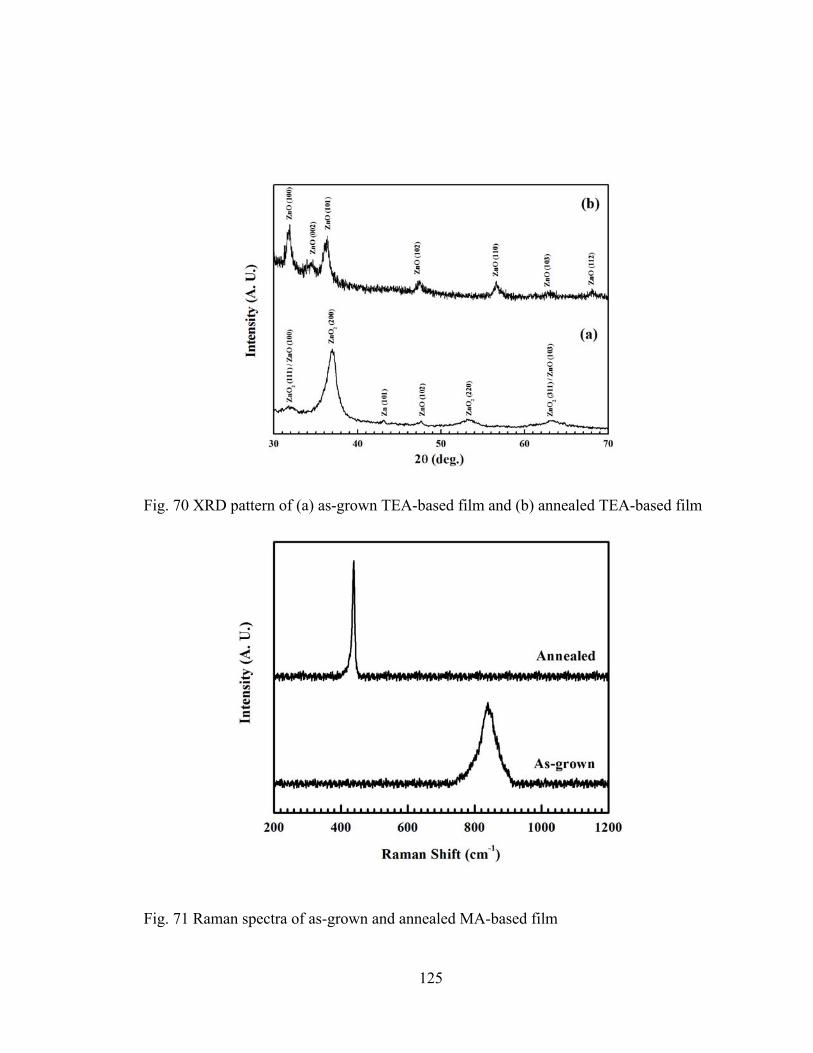
125
Fig. 70 XRD pattern of (a) as-grown TEA-based film and (b) annealed TEA-based film
Fig. 71 Raman spectra of as-grown and annealed MA-based film

126
Table 24 A summary of XRD data for standard cubic ZnO2, hexagonal ZnO, elemental Zn, and as-grown and annealed TEA-based film Sample 2θ (deg.) d (nm) I/Io (%) (hkl) Sample 2θ (deg.) d (nm) I/Io (%)
ZnO2 (*C) 31.794 0.28123 65.5 ( 1 1 1) As-grown 31.786 0.28129 10.6 36.876 0.24355 100.0 ( 2 0 0) 36.950 0.24308 100.0
Zn (*H) 43.220 0.20915 100.0 ( 1 0 1) 43.147 0.20950 7.1
ZnO (†H) 47.535 0.19113 21.1 ( 1 0 2) 47.547 0.19108 7.9
ZnO2 (*C) 53.139 0.17222 44.1 ( 2 2 0) 53.142 0.17221 7.5 63.268 0.14687 39.1 ( 3 1 1) 63.350 0.14669 6.7
ZnO (†H) 31.766 0.28147 56.5 ( 1 0 0) Annealed 31.761 0.28151 89.2 34.419 0.26036 41.5 ( 0 0 2) 34.437 0.26022 21.9 36.250 0.24761 100.0 ( 1 0 1) 36.379 0.24676 100.0 47.535 0.19113 21.1 ( 1 0 2) 47.459 0.19141 26.1 56.590 0.16251 30.5 ( 1 1 0) 56.638 0.16238 39.3 62.851 0.14774 26.8 ( 1 0 3) 62.739 0.14798 15.0 67.941 0.13786 21.7 ( 1 1 2) 68.041 0.13768 21.1
*C = Cubic [ 168], *H = Hexagonal [ 169], †H = Hexagonal [ 170]
After annealing, the peak at 840 cm-1 disappeared and only one peak at 437.2 cm-1
was observed, which is the characteristic peak of the non-polar Raman active E2-high
mode of ZnO [ 171, 172]. A Lorentzian fit of the peaks at 840 cm-1 and 437.2 cm-1
showed a FWHM of 58.7 cm-1 and 7.8 cm-1, respectively. The observed reduction in
FWHM after annealing indicates an enhancement in film crystallinity as is suggested by
the SEM and the transmittance measurements reported earlier (Fig. 67 & Fig. 68). It
should be noted that the baseline noise in the micro-Raman spectra is estimated to be
about 6% of the peak height. As a result, bearing in mind that the relative intensity of the
(102) peak of ZnO to that of the (200) peak of ZnO2 in the as-grown film is about 7.9 %
(Table 24), it is not surprising that no vibration modes of ZnO were observed for the as-
grown films. Such low percentage of the hexagonal phase of ZnO in the as-grown film

127
compared to that of the cubic phase of ZnO2 may be the reason for not detecting any
vibration modes of ZnO in the as-grown films.
Fig. 72 shows the RBS spectra of N2H4-based film annealed at 400°C in air for
one hour. Simulation using Rutherford Universal Manipulation Program (RUMP) [ 121]
was implemented to obtain the best possible match to the raw RBS spectra. As shown,
the Zn: O ratio obtained for the annealed film was (1.00: 1.25 ±0.01). Since ZnO films
are inherently n-type in nature which is due to either oxygen deficiency in the film or zinc
ions existing in interstitial positions, a ratio of Zn: O less than unity was unexpected.
RBS carried out on films grown using MA as well as NH3 that are annealed under the
same conditions (not shown in this work), also detected more oxygen content than zinc in
both films. Because of their high resistivity, we were not able to perform Hall
measurements on films annealed at 400 °C.
Although both XRD and micro-Raman spectroscopy are suggesting that as-grown
films are mainly zinc peroxide, FTIR absorption spectroscopy of MA-based as-grown
film, as shown in Fig. 73, detects a broadband around 3300 cm-1 which is assigned to the
O-H stretching mode of the hydroxyl group. This suggests that as-grown films may
consist of a mixture of zinc peroxide and zinc hydroxide. Peaks detected between 2840
cm-1 and 2930 cm-1 are due to the C-H stretching vibration mode, which corresponds to
the CH3 group of Methylamine. Similar observation has been reported earlier by Ortega-
López and Morales-Acevedo [ 161], where they detected a broad absorption band with a
peak at 3354 cm-1 related to the longitudinal stretching mode (3380 cm-1) of the OH
group. Xiong et al. [ 173] observed the same stretching mode at 3500 cm-1 for ZnO
nanoparticles grown via plasma synthesis.

128
100 200 300 400 500 600 700Channel
0
5
10
15
20
25
30
35
Nor
mal
ized
Yie
ld
0.5 1.0 1.5Energy (MeV)
Zn
O
ZnO - N2H4
(Zn: O = 1.00: 1.25)
Fig. 72 RBS spectrum and RUMP simulation of annealed N2H4-based film
Fig. 73 FTIR absorbance spectrum of as-grown MA-based film

129
Fig. 74 (a) XPS multiplex spectra of O 1s of as-grown and annealed TEA-based film, (b) XPS multiplex spectra of Zn 2p3/2 of as-grown and annealed TEA-based film, and (c) deconvolution of the O 1s peak of annealed TEA-based film

130
Fig. 74 (a) shows the XPS multiplex spectra of the O 1s peak for as-grown as well
as annealed TEA-based film. The binding energy of the O 1s peak of as-grown film is
located at 532.0 eV. According to Dupin et al. [ 174], binding energies of the O 1s peak
in the range of 527.7 eV to 530.6 eV are characteristics of O −2 oxides, and binding
energies in the range of 530.6 eV to 531.1 eV are characteristics of oxygen species
integrated in the material as OH − or O −22 , while binding energies in the range of 531.1
eV to 532.0 eV are due to low coordinated oxygen ions that could be described as “O − ”
species. However, it should be noted that binding energies as high as 532.8 eV and 533.6
eV have been reported earlier for peroxides and hydro-peroxides at polymer surfaces
[ 175].
Therefore, considering the findings of the XRD and micro-Raman (Fig. 70 & Fig.
71), we believe that the binding energy observed in this work at 532.0 eV is attributed to
zinc peroxide. A shift of about 2.0 eV was observed for the O 1s peak of annealed film.
Fig. 74 (b) shows the XPS multiplex of the Zn 2p3/2 peak. The binding energy of the Zn
2p3/2 of the as-grown film was observed at 1022.2 eV, while the binding energy
associated with the Zn 2p3/2 peak of the annealed film is 1021.8 eV, which indicates a
small shift of 0.4 eV after annealing. Both values are within the range of binding energy
characteristics of ZnO [ 148].
Since the O 1s peak of annealed film is asymmetric, a deconvolution of this peak
was carried out, as shown in Fig. 74 (c). As shown, deconvolution of the O 1s peak of
annealed ZnO film renders two doublets with the main doublet located at 530.0 eV, and
the smaller one located at 531.8 eV. The contribution observed at 530.0 eV is a

131
characteristic of O −2 oxides [ 148, 174], while the contribution at 531.8 eV is due to
either peroxide or “O − ” species. This explains the excess oxygen content in the ZnO
film after annealing at 400 °C that was detected by RBS (Fig. 72). Since it is widely
believed that zinc peroxide completely decomposes into zinc oxide at annealing
temperatures higher than 200 °C [ 163- 165], we believe that the contribution at 531.8 eV
is mainly due to low coordinated “O − ” species, as suggested by Dupin et al. [ 174]. The
presence of such low coordinated “O − ” species in the film could be attributed to the
chemisorption of oxygen at the grain boundaries during the CBD process [ 19, 176].
High resolution transmission electron microscopy (HRTEM) of NH3-based ZnO
film that was annealed at 400 °C in air is shown in Fig. 75 (a). As shown, the ZnO layer
is about 0.2 µm and the average grain size is about 10 nm. Only small variations in film
thickness are observed, which are in the range of the 10 nm average grain diameter.
Occasional cracks due to annealing are found at the surface of the film, which typically
extend about half way into the ZnO layer.
The electron diffraction pattern observed (Inset of Fig. 75 (a)) confirms that the
ZnO film is polycrystalline with a hexagonal crystal lattice. The Fourier-filtered
HRTEM image in Fig. 75 (b) shows the crystal structure of the individual ZnO grains and
their size.
As mentioned earlier, films annealed at 400 °C were highly resistive and, as a
result, performing Hall measurements on such films was not possible. Therefore, films
used for Hall measurements were further annealed at 500 °C in argon ambient for one
hour.

132
Fig. 75 (a) HRTEM and TEM diffraction pattern (inset) of annealed NH3-based ZnO film, and (b) Fourier-filtered HRTEM of annealed NH3-based ZnO film (low boundary is glass substrate)

133
Table 25 Hall effect measurements of NH3, N2H4, MA and TEA-based annealed undoped ZnO and Al-doped ZnO films
Sample Carrier Density (cm-3)
Mobility (cm2/V-S)
Resistivity (Ω-cm)
NH3-based 1.52 x 10¹⁹ 1.01 x 10⁻¹ 4.04 x 100 MA-based 2.03 x 10¹⁸ 1.37 x 10⁻¹ 2.23 x 101 TEA-based 1.02 x 10¹⁹ 9.44 x 10⁻¹ 6.48 x10⁻¹ N2H4-based 2.24 x 10¹⁹ 1.1 x 10⁻² 2.51 x 101 Al-doped 2.49 x 10¹⁹ 2.69 x 100 9.32 x10⁻²
Table 25 shows the carrier density, resistivity, and Hall mobility of undoped films
grown using ammonia, N2H4, MA and TEA. Table 25 also shows the Hall measurements
carried out for Al-doped TEA-based ZnO film grown at [Al] / [Zn] ratio of ~ 0.008. As
shown, all films show high carrier density and low resistivity for CBD undoped ZnO
films. A carrier density as high as 2.24 x 1019 cm-3 and a resistivity as low as 6.48 x10⁻¹
Ω-cm were obtained for undoped films. Resistivity of Al-doped film, however, was one
order of magnitude less than the smallest resistivity achieved for undoped films. This
may be a good indication that future in-situ doping of CBD-ZnO films using group III
elements, such as aluminum, boron, indium, or gallium may reduce the resistivity further
to achieve a transparent conducting CBD-ZnO thin films.
4.1.4 Conclusion
CBD of ZnO thin films using six different complexing agents is investigated. Four of
these six ligands proved to be successful where high quality; adherent, uniform,
transparent, and specularly reflecting ZnO films were obtained. As-grown films were
mainly ZnO2 with a band gap around 4.3 eV. Films annealed at 400 °C were ZnO with a
band gap around 3.3 eV. XRD and micro-Raman revealed that as-grown film mainly
consists of cubic ZnO2 that was transformed into hexagonal ZnO after annealing. FTIR

134
of as-grown film, however, showed a broad absorption band around 3300 cm-1, which is
assigned to the O-H stretching mode of the hydroxyl group suggesting that as-grown film
may consist of a mixture of ZnO2 and Zn(OH)2. RBS detected excess oxygen content in
ZnO films after annealing. XPS spectra were found to be consistent with the RBS
observations of annealed films. HRTEM showed small variations in film thickness; in
the range of the 10 nm average grain diameter. Occasional cracks, due to annealing, are
found at the surface of the film, which typically extend about half way into the ZnO
layer. The electron diffraction pattern observed confirms only a slight texture of the
crystal lattice with respect to the substrate. A carrier density as high as 2.24 x 1019 cm-3
and a resistivity as low as 6.48 x10⁻¹ Ω-cm were obtained for annealed ZnO films. One
of the challenges we have faced in this work is the strong alkalinity of our solutions that
prevented us from growing thicker ZnO films using multi-dip deposition; any attempt to
dip the original film in a fresh solution to grow another layer of ZnO resulted in
immediate etching of the original layer and a subsequent deposition of a non-uniform and
a porous new ZnO layer with inferior quality. Therefore, in this work, we were limited to
one single deposition with a film thickness that ranged from 0.2 µm to 0.7 µm. Another
challenge was the occasional cracks that appear in ZnO films after annealing, as was
revealed by SEM and TEM of annealed MA-based and NH3-based ZnO films (Fig. 67 (a)
& Fig. 75 (a), respectively). This, in turn, has a dramatic effect on film Hall mobility, as
shown (Table 25). One more challenge we faced is the unexpected excess oxygen
content in ZnO films after annealing which resulted in a Zn: O ratio less than unity. As a
result, films annealed at 400 °C in air were highly resistive and further annealing at 500
°C in argon ambient was necessary for Hall measurements to be attainable. We believe

135
that more careful post-heat treatments as well as in-situ doping of such CBD-ZnO films
using group III elements, such as aluminum, boron, indium, or gallium may reduce the
resistivity further where a transparent conducting CBD-ZnO is achievable.

136
4.2 Investigation of Chemical Bath Deposition of CdO Thin Films Using Three Different Complexing Agents
4.2.1 Introduction
Chemical bath deposition (CBD) is the analog in liquid phase of the well-known
chemical vapor deposition technique in the vapor phase. Among all techniques used to
grow group II-VI semiconductors, CBD has the advantage of being a simple, low
temperature, and inexpensive large-area deposition technique. It has been employed in
the deposition of semiconductor thin films for over forty years [ 18]. CBD has been
extensively used in growing Group II-VI semiconductors, such as CdS [ 18, 20- 24], CdSe
[ 48- 51], HgS [ 60, 61], HgSe [ 62, 63], ZnS [ 64- 67], ZnSe [ 76- 79], and ZnO [ 84- 88].
CdO thin films reported in the literature have been obtained mainly by dc
magnetron reactive sputtering [ 177], metal organic chemical vapor deposition [ 178, 179],
vacuum evaporation [ 180], electrochemical deposition [ 181], pulsed laser deposition
[ 182], electron beam evaporation [ 183], spray pyrolysis [ 184], sol-gel [ 185], RF
magnetron sputtering [ 186], and successive ionic layer adsorption and reaction [ 187].
However, only few attempts to grow CdO thin films using CBD have been reported [ 55-
58], where only ammonia has been used as complexing agent.
In this work, we report CBD of CdO using three different complexing agents,
namely ammonia, ethanolamine (EA), and methylamine (MA). Transmittance,
reflectance measurements and band gap calculations are carried out for as-grown films as
well as annealed films. Resistivity, carrier density, and Hall mobility of annealed films
are acquired using Hall effect measurements. Crystal structure as well as crystal quality
are determined using X-ray diffraction, transmission electron microscopy, and Fourier

137
transform infrared spectroscopy. Film morphology, composition, and binding energy are
studied using scanning electron microscopy, Rutherford backscattering spectroscopy, and
X-ray photoelectron spectroscopy, respectively.
4.2.2 Experimental Details
CdO films were prepared using aqueous solutions of CdSO4 (0.038 M), (NH4)2SO4
(0.076 M), H2O2 (34%), and NH4OH (29.4 %). Each bath contained 100-120 ml of de-
ionized water (resistivity ~ 18.2 MΩ-cm) that was kept under stirring at 85 °C. In
addition to ammonia, two other complexing agents were used; EA and MA. To ensure
stable Cd[NH3] 24+ complex in the main solution, ammonia was added whenever EA or
MA is being used. Similar to our previous work on CBD-ZnO [ 84], It was noticed that
adding ammonia is necessary to dissolve the Cd(OH)2 formed upon mixing the Cd-source
and EA or MA. CdSO4, (NH4)2SO4, and the desired complexing agent were mixed at
room temperature before being added to the main solution. Appropriate amounts of
hydrogen peroxide were then added to the main solution. Films were grown on 38 mm x
38 mm x 1 mm glass substrates (Schott Borofloat glass). With the help of a Teflon
holder, the glass substrate was kept vertically in the solution. All substrates were held in
the bath prior to the addition of any of the reagents. To ensure deposition of high-quality,
adhesive, and specularly reflecting films, the substrate was removed from the solution
when the solution becomes turbid and the homogeneous reaction starts to take place. The
cleaning steps of the substrate are reported elsewhere [ 22].
Details of the specular transmittance/reflectance measurements, bandgap
calculations, Hall effect measurements, XRD, SEM, and XPS measurements are

138
mentioned in sec. 3.1.2. Details of the TEM measurements are reported in sec. 3.2.2.
Details of the RBS measurements can be found in sec. 2.1.2. Details of the FTIR micro-
analysis are mentioned in sec. 4.1.2.
4.2.3 Results and Discussion
Fig. 76 shows the optical transmittance of as-grown films for all three complexing agents.
As shown, all three films exhibit high transmittance that exceeds 80% in the visible
region. The NH3-based and EA-based films exhibit a sharp absorption edge around 365
nm – 370 nm, while the absorption edge of the MA-based film is around 270 nm. Such
high transmittance and sharp absorption edge observed indicate the high quality of all
three films. The calculated bandgap is 3.37 eV, 3.40 eV, and 4.64 eV for the EA-based,
NH3-based, and MA-based film respectively. The blue shift observed in the case of MA-
based films can be understood by comparing its XRD pattern to that of EA-based film.
According to Fig. 77, the as-grown EA-based film consists of a mixture of three different
phases; cubic CdO [ 188], monoclinic / hexagonal Cd(OH)2 [ 189, 190], and cubic CdO2
[ 191]. However, as shown in Fig. 78, only cubic phase of CdO2 is detected for as-grown
MA-film. It should be noted that the XRD pattern of as-grown NH3-film (not shown in
this work) is similar to that of EA-based film. This may explain why both films almost
share the same absorption edge, while a blue shift of more than 1.2 eV is observed in the
case of MA-based film. After annealing at 400 °C in air for one hour, all three films are
fully transformed into CdO. Fig. 79 shows the XRD pattern of annealed EA-based film,
with only cubic phase of CdO [ 192] being detected. Similar XRD patterns are obtained
for both MA-based and NH3-based films annealed under the same conditions.

139
Fig. 76 Specular transmittance of as-grown films deposited using three different complexing agents
Fig. 77 XRD pattern of as-grown EA-based film

140
Fig. 78 XRD pattern of as-grown MA-based film
Fig. 79 XRD pattern of annealed EA-based film

141
Such transformation to CdO after annealing is responsible for the red shift
observed in the optical transmittance (Fig. 80) and the optical bandgap (Fig. 81) of EA-
based film. The bandgap of annealed CdO films is 2.53 eV, which agrees with the 2.55
eV [ 58], 2.57 eV [ 55], and 2.58 eV [ 158] bandgap values reported earlier in the literature
for CdO.
FTIR absorption measurements shown in Fig. 82 agree with the XRD findings.
Similar to what we have previously observed for CBD-ZnO [ 84], FTIR of as-grown EA-
based film (Fig. 82 a) detects a broadband around 3300 cm-1 which is assigned to the O-H
stretching mode of the hydroxyl group. This confirms the presence of the Cd(OH)2 phase
in as-grown EA-based films. This broadband disappears after annealing, as shown in Fig.
82 (b). However, as shown in Fig. 82 (c), such broadband does not exist in the case of
as-grown MA-based film. It should be noted that peaks detected between 2840 cm-1 and
2930 cm-1 (Fig. 82 a) are due to the C-H stretching vibration mode, which corresponds to
the CH2 group of ethanolamine, which disappears after annealing as EA-film is fully
transformed into CdO. Absorbance peaks observed between 650 cm-1 and 1500 cm-1 are
due to Si-O and B-O stretching vibrations [ 193] from the Borofloat glass substrate. It is
worth noting that the boron content of Borofloat glass is about 5.2%.
Fig. 83 shows the RBS spectra of as-grown EA-based film. Simulation using
Rutherford Universal Manipulation Program (RUMP) [ 121] was implemented to obtain
the best possible match to the raw RBS spectra. As shown, the Cd: O ratio obtained for
the as-grown film is (1.00: 1.74 ±0.01). This confirms the presence of CdO in as-grown
EA-based films. Should the film contains only mixed phases of CdO2 and Cd(OH)2, a
ratio of about (1.00: 2.00) will be observed.

142
Fig. 80 Specular transmittance and reflectance of as-grown and annealed EA-based film
Fig. 81 Optical band gap calculations of as-grown and annealed EA-based film

143
Fig. 82 FTIR absorbance spectrum of (a) as-grown EA-based film, (b) annealed EA-based film, and (c) as-grown MA-based film
200 400 600 800Channel
0
10
20
30
40
50
60
70
Nor
mal
ized
Yie
ld
0.5 1.0 1.5 2.0Energy (MeV)
Cd
O
EA-film (as-grown)(Cd: O = 1.00: 1.74)
Fig. 83 RBS spectrum and RUMP simulation of as-grown EA-based film

144
Such ratio is obtained in the case of as-grown MA-based film (not shown in this
work). Fig. 84, however, shows RBS of MA-annealed film, where a ratio of (1.00: 1.00
±0.01) is observed. This indeed confirms that, after annealing at 400 °C in air, film is
fully transformed into CdO.
The XPS multiplex spectra of the Cd 3d5/2 and 3d3/2 peaks of as-grown as well as
annealed EA-based films are shown in Fig. 85. As shown, Cd 3d5/2 and 3d3/2 peaks of the
annealed film are symmetric and located at 405 eV and 411.8 eV which agrees well with
the 6.74 eV spin-orbit energy splitting between Cd 3d5/2 and 3d3/2 states [ 148]. However,
both peaks of as-grown film are asymmetric. As shown in Fig. 86, deconvolution of the
Cd 3d5/2 peak renders three peaks with binding energies of 403.7 eV, 404.5 eV, and 405.4
eV. These three binding states can be assigned to CdO2, Cd(OH)2, and CdO, respectively
[ 148]. This also confirms the XRD, FTIR, and RBS findings of the mixed phase nature
of as-grown EA-based film. Similar deconvolution carried out for the Cd 3d3/2 peak is
also shown in Fig. 86. All three peaks obtained maintain a ~ 6.7 eV energy difference
from their corresponding Cd 3d5/2 peaks. Finally, it should be noted that both 405.4 eV
and 405 eV values observed in as grown and annealed films lie within the accepted
values of Cd 3d5/2 binding energies of CdO [ 148].
Fig. 87 shows the XPS multiplex spectra of the O 1s peak for as-grown and
annealed EA-based films. Similar to the Cd 3d peaks, the O 1s peak of annealed film is
symmetric while that of as-grown films is asymmetric. The O 1s binding energy of
annealed film is at 529.9 eV, which lies within the 527.7 eV to 530.6 eV range
characteristic of O −2 oxides [ 148, 174].

145
200 400 600 800Channel
0
10
20
30
40
50
Nor
mal
ized
Yie
ld
0.5 1.0 1.5 2.0Energy (MeV)
Cd
O
MA-film (annealed)(Cd: O = 1.00: 1.00)
Fig. 84 RBS spectrum and RUMP simulation of annealed MA-based film
Fig. 85 XPS multiplex spectra of Cd 3d of as-grown and annealed EA-based film

146
Fig. 86 Deconvolution of the Cd 3d peaks of as-grown EA-based film
Fig. 87 XPS multiplex spectra of O 1s of as-grown and annealed EA-based film

147
As shown in Fig. 88, a deconvolution of the O 1s peak of as-grown film renders
two doublets with the main doublet located at 531.1 eV and the smaller one located at
528.4 eV. According to Dupin et al. [ 174], binding energies in the range of 530.6 eV to 531.1
eV are characteristics of oxygen species integrated in the material as OH − or O −22 . Therefore,
the main contribution observed at 531.1 eV is due to either cadmium peroxide or
cadmium hydroxide, while the contribution at 528.4 eV is characteristic of cadmium
oxide, which again agrees with the XRD, FTIR, and RBS findings of the mixed phase
nature of as-grown EA-based film.
HRTEM image of annealed EA-film is shown in Fig. 89. As shown, the CdO
layer is about 0.25 µm. Only small variations in film thickness are observed. Occasional
cracks due to annealing are found, as indicated by arrows near the edge of the film. The
electron diffraction pattern observed (Inset of Fig. 89) confirms that CdO film is
polycrystalline with a cubic crystal lattice.
SEM micrographs of annealed MA, EA, and NH3-based films are shown in Fig.
90. As shown, MA and EA-based films maintain their integrity after annealing while
NH3-based films deteriorate when annealed, as indicated by the high density of cracks
shown in Fig. 90 (c). This could be attributed to stress in as-grown NH3-based films,
which caused films to lose their integrity after annealing. We have reported similar
observation for EA-based ZnO films in a previous work [ 84]. Some pinholes have been
observed in MA-based film (Fig. 90 a). It is also noticed that, when compared to EA-
film, average grain size of MA-film is much smaller. EA-based film, however, is
continuous with much smoother surface than the other two films. This will have a
significant impact on film resistivity and mobility as will be shown.

148
Fig. 88 Deconvolution of the O 1s peak of as-grown EA-based film
Fig. 89 HRTEM and TEM diffraction pattern (inset) of annealed EA-based CdO film

149
Fig. 90 SEM micrographs of (a) annealed MA-based film, (b) annealed EA-based film, and (c) annealed NH3-based film

150
Table 26 Hall effect measurements of annealed EA, MA and NH3-based CdO films
Sample Carrier density (cm-3)
Mobility (cm2V-1S-1)
Resistivity (Ω-cm)
EA-based 1.89 x 10²⁰ 3.17 x 100 1.04 x 10⁻² MA-based 4.35 x 10¹⁸ 3.91 x 10⁻¹ 3.67 x 100 NH3-based 7.55 x 10¹⁷ 8.21 x 10⁻¹ 1.01 x 101
Table 26 shows the carrier density, resistivity, and Hall mobility of annealed EA,
MA, and NH3-based films as revealed by Hall measurements carried out at room
temperature. As shown, EA-films have the highest mobility and lowest resistivity
amongst all three films. Resistivity of MA-film is two orders of magnitude higher, while
that of NH3-films is three orders of magnitude higher. Hall mobility of both films is also
much smaller than that of EA-film. We believe that pinholes, small grain size, and high
density of cracks observed under SEM (Fig. 90 (a) & (c)) are responsible for such drop in
film resistivity and Hall mobility. High carrier density observed in EA-film can be
attributed to oxygen deficiency in the film due to annealing. It is widely believed that
excess Cd content in CdO film will result in Cd ions occupying interstitial sites where
they act as donors which, in turn, increases carrier density and lowers film resistivity.
SEM and Hall results suggest that EA-based CdO films are the best candidates for
fabricating transparent conducting oxides using a simple technique such as chemical bath
deposition. These films are found to be of high quality, good uniformity, exhibit high
transmittance, and good crystallinity. In addition, high conductivity is observed in EA-
based films where a carrier density as high as 1.89 x 1020 cm-3 and a film resistivity as
low as 1.04 x 10⁻² Ω-cm are achievable.

151
4.2.4 Conclusion
CBD of CdO using three different complexing agents is investigated. All three
complexing agents proved to be successful where high quality; adherent, uniform,
transparent, and specularly reflecting CdO films were obtained. XRD revealed that As-
grown EA-based films consist of mixture of cubic CdO2, cubic CdO, and monoclinic /
hexagonal Cd(OH)2 while only cubic CdO2 phase has been detected in as-grown MA-
based film. Annealing at 400 °C in air for one hour fully transformed as-grown films into
cubic CdO. Optical bandgap of as-grown EA, NH3, and MA-based films are 3.37 eV,
3.40 eV, and 4.64 eV, respectively. Annealed films have optical bandgap of 2.53 eV.
Both as-grown and annealed films exhibit high transmittance that exceeds 80% in the
visible region.
FTIR of as-grown EA-based film showed a broad absorption band around 3300
cm-1, which is assigned to the O-H stretching mode of the hydroxyl group confirming the
Cd(OH)2 phase detected by XRD. Such absorption band disappeared after annealing and
did not exist in as-grown MA-based film. RBS observations are consistent with the XRD
and FTIR results. Deconvolution of the XPS multiplex of Cd 3d and O 1s peaks of as-
grown EA-based film revealed three binding states of CdO2, Cd(OH)2, and CdO, two of
which disappeared after annealing which agree with the observations of XRD, FTIR, and
RBS. HRTEM showed small variations in film thickness and occasional cracks, due to
annealing. The electron diffraction pattern observed confirms the polycrystalline nature
of the CdO film. SEM micrographs show high density of cracks in annealed NH3-based
film. Some pinholes were detected in annealed MA-based films. SEM and Hall results
revealed that EA-based CdO films are the best candidates for fabricating transparent

152
conducting oxides using CBD, where a carrier density as high as 1.89 x 1020 cm-3 and a
film resistivity as low as 1.04 x 10⁻² Ω-cm are achievable.

153
4.3 Investigation of Chemical Bath Deposition of SnO2 and Cd2SnO4 Thin Films
4.3.1 Introduction
Transparent conducting oxides (TCO) such as indium tin oxide (ITO) play an important
role in solar cells, light emitting diodes, as well as other optoelectronic devices. Seeking
alternatives to ITO has been the focus of attention for a long time. As a result, other TCO
layers such as ZnO, CdO, and Cd2SnO4 are heavily investigated. Although several
techniques are currently in use to grow such layers, chemical bath deposition present a
simple, low temperature, and inexpensive large-area deposition alternative. For over
forty years, it has been widely used to grow group II-VI semiconductors, such as CdS
[ 18, 20- 47], CdSe [ 48- 54], CdO [ 55- 58], HgS [ 59- 61], HgSe [ 54, 62, 63], ZnS [ 64- 75],
ZnSe [ 76- 83], and ZnO [ 84- 94].
In a previous work [ 84], we investigated CBD of ZnO using six different
complexing agents, four of which proved to be successful in growing high quality ZnO
thin films with a bandgap of 3.3 eV, a carrier density as high as 2.24 x 1019 cm-3, and a
resistivity as low as 6.48 x 10⁻¹ Ω-cm. In another work [ 194], we succeeded to grow
CBD-CdO thin films using three different complexing agents. Annealed CdO films have
a bandgap of 2.53 eV, a carrier density as high as 1.89 x 1020 cm-3, and a resistivity as
low as 1.04 x 10⁻² Ω-cm.
SnO2 thin films reported in the literature have been obtained mainly by RF
magnetron sputtering [ 195], metal organic chemical vapor deposition [ 196], vacuum
evaporation [ 197], pulsed laser deposition [ 198], pulsed electron beam deposition [ 199],
spray pyrolysis [ 200], sol-gel [ 201], chemical vapor deposition [ 202], and successive

154
ionic layer adsorption and reaction [ 203]. However, very few attempts to grow SnO2 thin
films using CBD have been reported [ 204, 205]. In both cases, the deposition time was
of the order of hours; 15-24 hours in the work of Tsukuma et al [ 204] and 5-12 hours in
the work of Supothina and De Guire [ 205]. Tsukuma et al [ 204] reported a growth rate
that ranged from 2 nm / h at 40 °C to 50 nm / h at 80 °C. Supothina and De Guire [ 205]
reported growing SnO2 films, 60-70 nm thick, after 12 hours of deposition, with a growth
rate of approximately 9 nm / h during the first 4 hours. Clearly, the small growth rate is a
big limitation to using CBD as a viable technique to grow SnO2 thin films.
In this work, we report a new approach of CBD-SnO2 that enabled us to grow a
0.2 µm thick SnO2 film using multi-dip deposition, with a deposition time as little as 8-10
minutes. We also investigate the possibility of fabricating a TCO layer of CBD-Cd2SnO4
by growing CBD-SnO2 layer first, followed by CBD-CdO layer, and then annealing at
different temperatures in air as well as in argon ambient.
Transmittance, reflectance measurements and band gap calculations are carried
out for as-grown films as well as annealed films. Resistivity, carrier density, and Hall
mobility of annealed films are acquired using Hall effect measurements. Crystal
structure as well as crystal quality are determined using X-ray diffraction, transmission
electron microscopy. Film morphology, composition, and binding energy are studied
using atomic force microscopy (AFM), Rutherford backscattering spectroscopy, and X-
ray photoelectron spectroscopy, respectively.

155
4.3.2 Experimental Details
SnO2 films were prepared using aqueous solutions of tin chloride pentahydrate (0.028
M). Each bath contained 120 ml of de-ionized water (resistivity ~ 18.2 MΩ-cm) that was
kept under stirring at 55 °C. Films were grown on 38 mm x 38 mm x 1 mm glass (Schott
Borofloat glass) as well as quartz substrates (supplied by Quartz Scientific Inc.). With
the help of a Teflon holder, the glass substrate was kept vertically in the solution. The
cleaning steps of the substrate are reported elsewhere [ 22]. To ensure deposition of high-
quality and adhesive films, the substrate was removed from the solution when the
solution becomes turbid and the homogeneous reaction starts to take place. The
deposition time was about 8-10 minutes. In order to grow SnO2 films with a ~ 0.2 µm
thickness, the deposition process was repeated four times, with fresh solutions being used
every time.
After annealing the SnO2 film at 500 °C in air for one hour, a 0.2 µm layer of
CdO is grown on top of the SnO2 layer using CBD. Both layers are then annealed at
different temperatures in air and in argon ambient so that cadmium diffuses into the SnO2
layer to form Cd2SnO4. CdO thin films are grown using ammonia and ethanolamine as
complexing agents, CdSO4 as cadmium source, (NH4)2SO4 as a buffer, and H2O2 as an
oxidation agent. Details of CBD of CdO thin films are reported elsewhere [ 194].
Details of the specular transmittance/reflectance measurements, bandgap
calculations, Hall effect measurements, XRD, and XPS measurements are mentioned in
sec. 3.1.2. Details of the TEM measurements are reported in sec. 3.2.2. Details of the
RBS measurements can be found in sec. 2.1.2. AFM images were acquired using Veeco
Multimode SPM in tapping mode.

156
4.3.3 Results and Discussion
It is worth noting that SnO2 films grown are extremely adhesive; highly concentrated
sulfuric acid (98 %) and nitric acid (96 %) could not etch them. Therefore, in order to
perform optical measurements, for example, two substrates were mounted together on the
Teflon sample holder so that there is deposition on only one side of the substrate. Film
thickness was determined using TEM, as will be shown later.
Fig. 91 shows the optical transmittance of as-grown and annealed SnO2 films as
well as CdO+SnO2 films annealed at 500 °C and 700 °C. As shown, all films exhibit
high transmittance that, in the case of SnO2 films, exceeds 90% in the visible region. A
red shift is observed due to formation of Cd2SnO4, which increases with increasing
annealing temperature. The sharp absorption edge observed in Cd2SnO4 indicates that
films still maintain high quality even after annealing at temperatures as high as 700 °C.
Films annealed at a temperature of 800 °C or higher did not maintain the same quality.
Fig. 92 shows the optical bandgap calculated for annealed SnO2 films as well as
CdO+SnO2 films annealed at 500 °C and 700 °C. As shown, the bandgap is 4.42 eV,
2.67 eV, and 2.52 eV, for annealed SnO2, Cd2SnO4 annealed at 500 °C, and 700 °C,
respectively. It should be noted that the bandgap we observed for CdO films annealed at
400 °C is 2.53 eV [ 194]. Clearly, as the annealing temperature increases, films tend to
behave more like CdO rather than Cd2SnO4. It should be noted that though the typical
bandgap of SnO2 is 3.6 eV, much higher bandgap values have been reported in the
literature. Rakhshani et al [ 206] reported a direct bandgap of 4.11 eV, while Dawar and
Joshi [ 207] reported bandgap values in the range of 3.9 eV – 4.6 eV for SnO2.

157
Fig. 91 Specular transmittance of as-grown and annealed SnO2 films and CdO+SnO2 films annealed at 500 °C and 700 °C
Fig. 92 Optical band gap calculations of annealed SnO2 films and CdO+SnO2 films annealed at 500 °C and 700 °C

158
Fig. 93 XRD pattern of annealed SnO2 film
200 400 600 800Channel
0
5
10
15
20
25
Nor
mal
ized
Yie
ld
0.5 1.0 1.5 2.0Energy (MeV)
Sn
Si
O
SnO2-annealed(Sn: O = 1.00: 2.00)
Fig. 94 RBS spectrum and RUMP simulation of annealed SnO2 film

159
The XRD pattern of annealed SnO2 film is shown in Fig. 93. Annealed film is
polycrystalline with a main (113) reflection and four weak reflections characteristic of the
(023), (200), (106), and (117) planes of orthorhombic SnO2 [ 208]. As grown SnO2 films
are found to be amorphous. Fig. 94 shows the RBS spectra of annealed SnO2 film.
Simulation using Rutherford Universal Manipulation Program (RUMP) [ 121] was
implemented to obtain the best possible match to the raw RBS spectra. As shown, the
film is highly stoichiometric with a Sn: O ratio of about (1.00: 2.00 ±0.01). The XPS
multiplex spectra of the Sn 3d5/2 and 3d3/2 peaks of annealed SnO2 film is shown in Fig.
95. As shown, Sn 3d5/2 and 3d3/2 peaks of the annealed film are symmetric and located at
486.4 eV and 494.8 eV which agrees well with the 8.41 eV spin-orbit energy splitting
between Sn 3d5/2 and 3d3/2 states [ 148]. Also, the observed binding energy of 486.4 eV
of Sn 3d5/2 lies within the accepted range of binding energy values for SnO2 [ 148]. Fig.
96 shows the XPS multiplex spectra of the O 1s peak of annealed SnO2 film. The O 1s
peak of annealed film is symmetric and located at 530.3 eV, which lies within the 527.7
eV to 530.6 eV range characteristic of O −2 oxides [ 148, 174].
2-D and 3-D AFM images of as-grown as well as annealed SnO2 film are shown
in Fig. 97 and Fig. 98, respectively. Both films are continuous, uniform, and relatively
smooth. The surface features of the films are comparable and the calculated surface
roughness values are ~ 37.5 nm and 26.8 nm for as-grown and annealed SnO2 films,
respectively. Clearly, annealing reduced film roughness. Occasional crystallite
overgrowth is observed on the surface of both films. This is attributed to colloidal
particulates formed in solution and then adsorbed on the film.

160
Fig. 95 XPS multiplex spectra of Sn 3d of annealed SnO2 film
Fig. 96 XPS multiplex spectra of O 1s of annealed SnO2 film

161
Fig. 97 2-D and 3-D AFM images of as-grown SnO2 film

162
Fig. 98 2-D and 3-D AFM images of annealed SnO2 film

163
Fig. 99 HRTEM and TEM diffraction pattern (inset) of annealed SnO2 film

164
HRTEM image of annealed SnO2 film is shown in Fig. 99. As shown, the SnO2
layer is about 0.20 µm. Film surface is uniform with only small variations in film
thickness being observed. The electron diffraction pattern observed (Inset of Fig. 99)
confirms that SnO2 film is polycrystalline with orthorhombic crystal lattice structure.
Table 27 Hall effect measurements of annealed CdO, SnO2, and Cd2SnO4 films
Sample Carrier density (cm-3)
Mobility (cm2V-1S-1)
Resistivity (Ω-cm)
CdO 1.89 x 10²⁰ 3.17 x 100 1.04 x 10⁻² SnO2 5.15 x 10¹² 1.61 x 101 7.53 x 10⁴
Cd2SnO4 3.74 x 10¹⁹ 3.49 x 10⁻¹ 4.78 x 10⁻¹
Table 27 shows Hall effect measurements carried out at room temperature for
CdO film annealed at 400 °C, SnO2 film annealed at 500 °C, and Cd2SnO4 layer annealed
at 500 °C. As shown, the carrier density and resistivity values of the Cd2SnO4 film are
intermediate between those of CdO film and SnO2 film. Clearly, using a simple
technique like CBD, we have succeeded to grow a TCO layer with a bandgap of ~ 2.7 eV
and a carrier density as high as 3.74 x 1019 cm-3 and a resistivity ~ 4.78 x 10⁻¹ Ω-cm.
4.3.4 Conclusion
CBD of SnO2 as well as Cd2SnO4 is investigated. A 0.2 µm thick CBD-SnO2 films are
grown using multi-dip deposition, with a deposition time as little as 8-10 minutes. Films
are extremely adhesive and cannot be etched. Films are highly transparent with a
bandgap of ~ 4.42 eV and a transmittance exceeding 90 % in the visible region of the
spectrum. Annealed films are orthorhombic with a preferred orientation along the [113]
direction. According to RBS data, annealed film is highly stoichiometric with a Sn: O

165
ratio of about (1.00: 2.00 ±0.01). AFM images show as-grown and annealed SnO2 films
to be continuous, uniform, and relatively smooth. An average roughness of ~ 37.5 and
26.8 nm is estimated for as-grown and annealed films, respectively. The electron
diffraction pattern observed under TEM confirms that SnO2 film is polycrystalline with
orthorhombic crystal lattice structure.
Cd2SnO4 layer with a wide bandgap of ~ 2.7 eV and a carrier density as high as
3.74 x 1019 cm-3 and a resistivity ~ 4.78 x 10⁻¹ Ω-cm is achieved using a simple technique
like CBD. Although promising, we believe that further work is needed to reach a
bandgap of ~ 3.0 eV or higher, and a resistivity of the order of 10-3 Ω-cm or lower, in
order to fabricate a viable CBD-TCO layer. This work merely reports a preliminary step
towards using CBD to fabricate a TCO layer of Cd2SnO4. Careful studies of post-heat
treatments as well as further investigations of CBD-Cd2SnO4 stoichiometry are still
needed to achieve this goal.

166
CONCLUSION
We have succeeded to optimize CBD of CdS thin films using NTA, NTA+N2H4, and
NTA+NH3. The effect of the cadmium salt on the deposition process of CdS has been
studied using four different cadmium sources. Higher growth rate is achieved when
CdSO4 is used as cadmium precursor. Films grown using CdSO4 have higher bandgap,
better crystallinity, higher mobility, and lower resistivity. Highly stoichiometric films are
obtained when CdCl2 as well as CdI2 are used as cadmium sources.
In-situ doping of CBD-CdS using group III elements, such as aluminum, boron,
and gallium proves to be successful. We have demonstrated that the dark resistivity of
CBD-CdS could be reduced by four orders of magnitude using this approach; a dark
resistivity of the order of 10-2 Ω-cm and a carrier density as high as ~ 1019 cm-3 are
achieved. We have also shown that due to extremely low solubility product of indium
sulfide (Ksp = 10-73.24) compared to that of Cadmium Sulfide (Ksp = 10-27.94) [ 96], it is
highly unlikely, if not impossible, to incorporate indium in CdS, using CBD.
CBD of ZnO using six different complexing agents has been investigated, four of
which prove to be successful. Adhesive, uniform, specularly reflecting, and transparent
high quality ZnO films are obtained. Aluminum in-situ doping of CBD-ZnO shows
promising results where a carrier density as high as 2.49 x 1019 cm-3 and a resistivity as
low as 9.32 x10⁻² Ω-cm are achieved.
CBD of CdO using three different complexing agents has been achieved. EA-
based CdO films are found to be the best candidates for fabricating transparent
conducting oxides using CBD, where a carrier density as high as 1.89 x 1020 cm-3 and a

167
film resistivity as low as 1.04 x 10⁻² Ω-cm are achievable. SnO2 thin films grown using
CBD are uniform, transparent, and extremely adhesive. Cd2SnO4 layer with a wide
bandgap of ~ 2.7 eV and a carrier density as high as 3.74 x 1019 cm-3 and a resistivity ~
4.78 x 10⁻¹ Ω-cm is achieved using CBD. Although promising, we believe that further
work is needed to reach a bandgap of ~ 3.0 eV or higher, and a resistivity of the order of
10-3 Ω-cm or lower, in order to fabricate a viable CBD-TCO layer.
We believe that our work on CBD of metal oxides, such as ZnO, CdO, and SnO2
merely serves as a preliminary step towards using CBD to fabricate a TCO layer of Al-
doped ZnO as well as Cd2SnO4.
Finally, we believe that the future of CBD resides in growing metal oxides as well
as TCO layers that could be used in the fabrication of light emitting diodes (LEDs) and
batteries. We also believe that, although difficult, fabricating and entire CIGS-based
solar cell using only CBD is possible. We have demonstrated that CBD of high quality
CdS, ZnO, CdO, SnO2, as well as Cd2SnO4 thin films is achievable. The challenge now
is to grow the CIGS absorber layer using CBD. We believe that the right approach is to
optimize CBD of copper sulfide, indium sulfide, and gallium sulfide separately. The next
step is to find the optimum pH value of the solution in each case that will ensure that film
grown will not be etched when dipped again in the solution, so that three different layers
of copper sulfide, indium sulfide, and gallium sulfide could be grown using the multi-dip
deposition approach. Post heat treatment of all three layers should result in the formation
of the CIGS layer.

168
Should this approach succeed, the goal of fabricating an entire solar cell device
using only CBD could become a reality. This indeed will have a significant impact on
solar cells industry.

169
APPENDIX A: COPYRIGHTS PERMISSION OF REFERENCE [ 15]

170

171
APPENDIX B: COPYRIGHTS PERMISSION OF REFERENCE [ 17]

172

173
REFERENCES:
1 M. Contreras, B. Egaas, K. Ramanathan, J. Hiltner, A. Swartzlander, F. Hasoon,
and R. Noufi, Prog. Photovolt: Res. Appl. 7, 311 (1999)
2 X. Wu, J. Keane, R. Dhere, D. Dehart, D. Albin, A. Duda, T. Gessert, S. Asher,
D. Levi, and P. Sheldon, Proceedings of the 17th European Photovoltaic Solar
Energy Conference, Munich, Germany, October 22-26 (2001), p. 995.
3 K. Ramanathan, M. Contreras, C. Perkins, S. Asher, F. Hasoon, J. Keane, D.
Young, M. Romero, W. Metzger, R. Noufi, J. Ward, and A. Duda, Prog.
Photovolt: Res. Appl. 11, 225 (2003)
4 J. Schrier, D. Demchenko, L. Wang, and A. Alivisatos, Nano Lett. 7, 2377 (2007)
5 U. Gangopadhyay, K. Kim, D. Mangalaraj, and J. Yi, Appl. Surf. Sci. 230, 364
(2004)
6 Q. Shen, J. Kobayashi, L. Diguna, and T. Toyoda, J. Appl. Phys. 103, 084304
(2008)
7 S. J. Jiao, Z. Z. Zhang, Y. M. Lu, D. Z. Shen, B. Yao, J. Y. Zhang, B. H. Li, D. X.
Zhao, X. W. Fan, and Z. K. Tang, Appl. Phys. Lett. 88, 031911 (2006)
8 W. Liu, S. L. Gu, J. D. Ye, S. M. Zhu, S. M. Liu, X. Zhou, R. Zhang, Y. Shi, Y.
D. Zheng, Y. Hang, and C. L. Zhang, Appl. Phys. Lett. 88, 092101 (2006)
9 N. Kh. Abrikosov, V. F. Bankina, L. V. Poretskaya, L. E. Shelimova, and E. V.
Skudnova, Semiconducting II-VI, IV-VI, and V-VI Compounds, Plenum Press,
New York (1969)

174
10 S. Ignatowicz and A. Kobendza, Semiconducting Thin Films of AIIBVI
Compounds, John Wiley & Sons, New York (1981)
11 Wikimedia commons; http://commons.wikimedia.org
12 C. Kittel, Introduction to Solid State Physics, John Wiley & Sons, New York
(1994)
13 N. W. Ashcroft and N. D. Mermin, Solid state physics, Brooks Cole, New York
(1976)
14 M. C. Tamargo, II-VI Semiconductor Materials and Their Applications, Taylor &
Francis, New York (2002)
15 S. Adachi, Properties of Group-IV, III-V, and II-VI Semiconductors, John Wiley
& Sons, Chichester (2005)
16 J. I. Pankove, Optical Processes in Semiconductors, Dover Publications, New
York (1971)
17 S. M. Sze, Physics of Semiconductor Devices, John Wiley & Sons, New York
(1981)
18 G. Kitaev, A. Uritskaya, and S. Mokrushin, Russ. J. Phys. Chem. 39, 1101 (1965)
19 R.S. Mane and C.D. Lokhande, Mater. Chem. Phys. 65, 1 (2000)
20 H. Khallaf, I. Oladeji, and L. Chow, Thin Solid Films 516, 5967 (2008)
21 H. Khallaf, I. Oladeji, G. Chai, and L. Chow, Thin Solid Films 516, 7306 (2008)
22 H. Khallaf, G. Chai, O. Lupan, L. Chow, S. Park, and A. Schulte, J. Phys. D:
Appl. Phys. 41, 185304 (2008)
23 H. Khallaf, G. Chai, O. Lupan, L. Chow, S. Park, and A. Schulte, Appl. Surf. Sci.
255, 4129 (2009)

175
24 H. Khallaf, G. Chai, O. Lupan, L. Chow, H. Heinrich, S. Park, and A. Schulte,
Phys. Stat. Sol. (a) 206, 256 (2009)
25 I. O. Oladeji, L. Chow, J. R. Liu, W. K. Chu, A. N. P. Bustamante, C.
Fredricksen, and A. F. Schulte, Thin Solid Films 359, 154 (2000)
26 I. Oladeji and L. Chow, Thin Solid Films 474, 77 (2005)
27 I. Oladeji and L. Chow, J. Electrochem. Soc. 144, 2342 (1997)
28 I. Kaur, D. Pandya, and K. Chopra, J. Electrochem. Soc. 127, 943 (1980)
29 C. Voss, Y. Chang, S. Subramanian, S. Ryu, T. Lee, and C. Chang, J.
Electrochem. Soc. 151, C655 (2004)
30 P. Nair, J. Campos, and M. Nair, Semicond. Sci. Technol. 3, 134 (1988)
31 P. O’Brien and T. Saeed, J. Cryst. growth 158, 497 (1996)
32 H. Zhang, X. Ma, and D. Yang, Mater. Lett. 58, 5 (2003)
33 P. Nemec, I. Nemec, P. Nahálková, Y. Nemcová, F. Trojánek, and P. Malý, Thin
Solid Films 403/404, 9 (2002)
34 S. Gorer and G. Hodes, J. Phys. Chem. 98, 5338 (1994)
35 R. Call, N. Jaber, K. Seshan, and J. Whyte, Sol. Energy Mater. 2, 373 (1980)
36 M. Nair, P. Nair, R. Zingaro, and E. Meyers, J. Appl. Phys. 75, 1557 (1994)
37 P. Roy and S. Srivastava, Mater. Chem. Phys. 95, 235 (2006)
38 J. Doña and J. Herrero, J. Electrochem. Soc. 139, 2810 (1992)
39 H. Metin and R. Esen, Semicond. Sci. Technol. 18, 647 (2003)
40 M. Rami, E. Benamar, M. Fahoume, F. Chraibi, and A. Ennaoui, Solid State Sci.
1, 179 (1999)
41 M. Nagao and S. Watanabe, Jpn. J. Appl. Phys. 7, 684 (1968)

176
42 R. Ortega-Borges and D. Lincot, J. Electrochem. Soc. 140, 3464 (1993)
43 T. Nakanishi and K. Ito, Sol. Energy Mater. Sol. Cells 35, 171 (1994)
44 C. Guillén, M. Martínez and J. Herrero, Thin Solid Films 335, 37 (1998)
45 T. Chu, S. Chu, N. Schultz, C. Wang, and C. Wu, J. Electrochem. Soc. 139, 2443
(1992)
46 M. Nair, P. Nair, and J. Campos, Thin Solid Films 161, 21 (1988)
47 A. Reádigos, V. García, O. Gomezdaza, J. Campos, M. Nair, and P. Nair,
Semicond. Sci. Technol. 15, 1022 (2000)
48 G. A. Kitaev and T. S. Terekhova, Russ. J. Inorg. Chem. 15, 25 (1970)
49 R. C. Kainthla, D. C. Pandya, and K. L. Chopra, J. Electrochem. Soc. 127, 277
(1980)
50 G. Hodes, A. Albu-Yaron, F. Decker, and P. Motisuke, Phys. Rev. B 36, 4215
(1987)
51 J. M. Gracia-Jiménez, G. Martinez-Montes, and R. Silva-González, J.
Electrochem. Soc. 139, 2048 (1992)
52 V. M. García, M. T. S. Nair, P. K. Nair, and R. A. Zingaro, Semicond. Sci.
Technol. 11, 427 (1996)
53 H. Cachet, R. Cortes, M. Froment, G. Maurin, and N. Shramchenko, J.
Electrochem. Soc. 144, 3583 (1997)
54 P. P. Hankare, V. M. Bhuse, K. M. Garadkar, S. D. Delekar, and I. S. Mulla,
Semicond. Sci. Technol. 19, 70 (2004)
55 M. Z. Najdoski, I. S. Grozdanov, and B. Minceva-Sukarova, J. Mater. Chem. 6,
761 (1996)

177
56 M. Ortega, G. Santana, and A. Morales-Acevedo, Solid-State Electron. 44, 1765
(2000)
57 M. Ocampo, A. M. Fernandez, and P. J. Sebastian, Semicond. Sci. Technol. 8,
750 (1993)
58 L. de León-Gutiérrez, J. Cayente-Romero, J. Peza-Tapia, E. Barrera-Calva, J.
Martínez-Flores, and M. Ortega-López, Mater. Lett. 60, 3866 (2006)
59 M. Perakh and H. Ginsburg, Thin Solid Films 52, 195 (1978)
60 S. S. Kale and C. D. Lokhande, Mater. Chem. Phys. 59, 242 (1999)
61 M. Z. Najdoski, I. S. Grozdanov, S. K. Dey, and B. B. Siracevska, J. Mater.
Chem. 8, 2213 (1998)
62 P. Pramanik and S. Bhattacharya, Mater. Res. Bull. 24, 945 (1989)
63 B. B. Pejova, M. Z. Najdoski, I. S. Grozdanov, and S. K. Dey, J. Mater. Chem. 9,
2889 (1999)
64 I. O. Oladeji and L. Chow, Thin Solid Films 339, 148 (1999)
65 P. O’Brien, D. J. Otway, and D. Smyth-Boyle, Thin Solid Films 361-362, 17
(2000)
66 J. M. Doña and J. Herrero, J. Electrochem. Soc. 141, 205 (1994)
67 I.C. Ndukwe, Sol. Energy Mater. Sol. Cells 40, 123 (1996)
68 S. Biswas, P. Pramanik, and P. K. Basu, Mater. Lett. 4, 81 (1986)
69 P K Nair and M T S Nair, Semicond. Sci. Technol. 7, 239 (1992)
70 O. L. Arenas, M. T. S. Nair and P. K. Nair, Semicond. Sci. Technol. 12, 1323
(1997)
71 Q. Liu, M. Guobing, and A. Jianping, Appl. Surf. Sci. 254, 5711 (2008)

178
72 A. Goudarzi, G. M. Aval, R. Sahraei, and H. Ahmadpoor, Thin Solid Films 516,
4953 (2008)
73 F. Göde, C. Gümüş, and M. Zor, J. Cryst. Growth 299, 136 (2007)
74 U. Gangopadhyay, K. Kim, D. Mangalaraj, and J. Yi, Appl. Surf. Sci. 230, 364
(2004)
75 J. Cheng, D. B. Fan, H. Wang, B. W. Liu, Y. C. Zhang, and H. Yan, Semicond.
Sci. Technol. 18, 676 (2003)
76 P. Pramanik and S. Biswas, J. Electrochem. Soc. 133, 350 (1986)
77 J. M. Doña and J. Herrero, J. Electrochem. Soc. 142, 764 (1995)
78 C. A. Estrada, P. K. Nair, M. T. S. Nair, R. A. Zingaro, and E. A. Meyers, J.
Electrochem. Soc. 141, 802 (1994)
79 A. M. Chaparro, M. A. Martínez, C. Guillén, R. Bayón, M. T. Gutiérrez, and J.
Herrero, Thin Solid Films 361-362, 177 (2000)
80 J. Herrero, M. T. Gutiérrez, C. Guillén, J. M. Doña, M. A. Martínez, A. M.
Chaparro, and R. Bayón, Thin Solid Films 361-362, 28 (2000)
81 C. D. Lokhande, P. S. Patil, A. Ennaoui, and H. Tributsch, Appl. Surf. Sci.
123/124, 294 (1998)
82 R. B. Kale, and C. D. Lokhande, Appl. Surf. Sci. 252, 929 (2005)
83 A. M. Chaparro, C. Maffiotte, M. T. Gutiérrez, and J. Herrero, Thin Solid Films
358, 22 (2000)
84 H. Khallaf, G. Chai, O. Lupan, H. Heinrich, S. Park, A. Schulte, and L. Chow, J.
Phys. D: Appl. Phys. 42, 135304 (2009)
85 T. Saeed and P. O’Brien, Thin Solid Films 271, 35 (1995)

179
86 P. O’Brien, T. Saeed, and J. Knowles, J. Mater. Chem. 6, 1135 (1996)
87 M. Ortega-López, A. Avila-García, M. Albor-Aguilera, and V. Resendiz, Mater.
Res. Bull. 38, 1241 (2003)
88 A. Ennaoui, M. Weber, R. Scheer, and H. Lewerenz, Sol. Energy Mater. Sol.
Cells 54, 277 (1998)
89 K. Govender, D. Boyle, P. Kenway, and P. O’Brien, J. Mater. Chem. 14, 2575
(2004)
90 A. Drici, G. Djeteli, G. Tchangbedji, H. Derouiche, K. Jondo, K. Napo, J.
Bernède, S. Ouro-Djobo, and M. Gbagba, Phys. Stat. Sol. (a) 201, 1528 (2004)
91 J. Ouerfelli, M. Regragui, M. Morsli, G. Djeteli, K. Jondo, C. Amory, G.
Tchangbedji, K. Napo, and J. Bernède, J. Phys. D: Appl. Phys. 39, 1954 (2006)
92 A. Peiró, C. Domingo, J. Peral, X. Domènech, E. Vigil, M. Hernández-Fenollosa,
M. Mollar, B. Marí, and J. Ayllón, Thin Solid Films 483, 79 (2005)
93 D. Chu, T. Hamada, K. Kato, and Y. Masuda, Phys. Stat. Sol. (a) 206, 718 (2009)
94 J. B. Chu, S. M. Huang, D. W. Zhang, Z. Q. Bian, X. D. Li, Z. Sun, and X. J. Yin,
Appl Phys A 95, 849 (2009)
95 T. P. Niesen and M. R. De Guire, J. Electroceramics 6, 169 (2001)
96 L. Sillén and A. Martell, Stability Constants of Metal-Ion Complexes, Burlington
House, London (1964)
97 G. Hodes, Chemical Solution Deposition of Semiconductor Films, Marcel
Dekker, New York (2003)
98 I. Oladeji, L. Chow, C. Ferekides, V. Viswanathan, and Z. Zhao, Sol. Energy
Mater. Sol. Cells 61, 203 (2000)

180
99 M. Contreras, M. Romero, B. To, F. Hasoon, R. Noufi, S. Ward, and K.
Ramanathan, Thin Solid Films 403/404, 204 (2002)
100 A. Davis, K. Vaccaro, H. Dauplaise, W. Waters, and J. Lorenzo, J. Electrochem.
Soc. 146, 1046 (1999)
101 O. Vigil-Galan, J. Larramendi, I. Riech, G. Rodriguez, A. Iribarren, J. Aguilar-
Hernandez, and G. Contreras-Puente, Semicond. Sci. Technol. 17, 1193 (2002)
102 O. Vigil-Galan, J. Ximello-Quiebras, J. Aguilar-Hernandez, G. Contreras-Puente,
A. Cruz-Orea, J. Mendoza-Alvarez, J. Cardona-Bedoya, C. Ruiz, and V.
Bermudez, Semicond. Sci. Technol. 21, 76 (2006)
103 R. Buckley and J. Woods, J. Phys. D: Appl. Phys. 6, 1084 (1973)
104 C. Tsai, D. Chuu, G. Chen, and S. Yang, J. Appl. Phys. 79, 9105 (1996)
105 R. Birkmire, B. McCandless, and S. Hegedus, Int. J. Sol. Energy 12, 145 (1992)
106 C. Dai, L. Horng, W. Hsieh, Y. Shih, C. Tsai, and D. Chuu, J. Vac. Sci. Technol.
A. 10, 484 (1992)
107 P. Boieriu, R. Sporken, Y. Xin, N. Browning, and S. Sivananthan, J. Elect.
Mater. 29, 718 (2000)
108 M. Ilieva, D. Dimova-Malinovska, B. Ranguelov, and I. Markov, J. Phys.:
Condens. Matter 11, 10025 (1999)
109 Y. Ma, A. Fahrenbruch, and R. Bube, Appl. Phys. Lett. 30, 423 (1977)
110 H. Uda, H. Yonezawa, Y. Ohtsubo, M. Kosaka, and H. Sonomura, Sol. Energy
Mater. Sol. Cells 75, 219 (2003)
111 M. Sasagawa and Y. Nosaka, Electrochim. Acta 48, 483 (2003)
112 S. Al Kuhaimi, Vacuum 51, 349 (1998)

181
113 J. Aguilar-Hernandez, G. Contreras-Puente, A. Morales-Acevedo, O. Vigil-
Galan, F. Cruz-Gandarilla, J. Vidal-Larramendi, A. Escamilla-Esquivel, H.
Hernandez-Contreras, M. Hesiquio-Garduno, A. Arias-Carbajal, M. Chavarria-
Castaneda, and G. Arriaga-Mejia, Semicond. Sci. Technol. 18, 111 (2003)
114 A. E. Martell and R. M. Smith, Critical Stability Constants, Plenum Press, New
York (1974)
115 A. Rakhshani and A. Al-Azab, J. Phys.: Condens. Matter 12, 8745 (2000)
116 S. Mokrushin and Y. Tkachev, Kolloidn. Zh. 23, 438 (1961)
117 G. Kitaev, S. Mokrushin, and A. Uritskaya, Kolloidn. Zh. 27, 51 (1965)
118 ICSD, 080-0019 (1997)
119 S. Chichibu, T. Mizutani, K. Murakami, T. Shioda, T. Kurafuji, H. Nakanishi, S.
Niki, P. Fons, and A. Yamada, J. Appl. Phys. 83, 3678 (1998)
120 E. F. Kaelble, Handbook of X-rays, McGraw-Hill, New York (1967)
121 L. Doolittle, Nucl. Instr. Methods B 15, 227 (1986)
122 I. Mártil, G. González-Díaz, and F. Sánchez-Quesada, J. Vac. Sci. Technol. A 2,
1491 (1984)
123 I. Mártil, G. González-Díaz, and F. Sánchez-Quesada, Thin Solid Films 114, 327
(1984)
124 P. Sebastian, Appl. Phys. Lett. 62, 2965 (1993)
125 D. Petre, L. Pintilie, E. Pentia, I. Pintilie, and T. Botila, Mater. Sci. Eng. B 58,
238 (1999)
126 S. Sahu and S. Chandra, Solar Cells 22, 163 (1987)
127 A. Shikalgar and S. Pawar, Solid State Commun. 32, 361 (1979)

182
128 B. Bargale, A. Shikalgar, and S. Pawar, Thin Solid Films 62, 215 (1979)
129 C. Lokhande and S. Pawar, Solid State Commun. 44, 1137 (1982)
130 J. Akintunde, J. Mater. Sci.: Mater. Electron. 11, 503 (2000)
131 J. Lee, Thin Solid Films 451-452, 170 (2004)
132 M. Ristova, M. Ristov, P. Tosev, and M. Mitreski, Thin Solid Films 315, 301
(1998)
133 M. Ristova and M. Ristov, Sol. Energy Mater. Sol. Cells 53, 95 (1998)
134 E. Bertrán, J. Morenza, J. Esteve, and J. Codina, J. Phys. D: Appl. Phys. 17, 1679
(1984)
135 T. Hayashi, T. Nishikura, T. Suzuki, and Y. Ema, J. Appl. Phys. 64, 3542 (1988)
136 O. Zelaya-Angel, J. Alvarado-Gil, R. Lozada-Morales, H. Vargas, and A.
Ferreira da Silva, Appl. Phys. Lett. 64, 291 (1994)
137 J. Huheey, Inorganic Chemistry, Harper & Row, New York (1983)
138 O. Zelaya-Angel, F. Castillo-Alvarado, J. Avendaño-López, A. Escamilla-
Esquivel, C. Contreras-Puente, R. Lozada-Morales, and G. Torres-Delgado, Solid
State Commun. 104, 161 (1997)
139 M. Froment, M. Bernard, R. Cortes, B. Mokili, and D. Lincot, J. Electrochem.
Soc. 142, 2642 (1995)
140 B. Tell, T. Damen, and S. Porto, Phys. Rev. 144, 771 (1966)
141 C. Arguello, D. Rousseau, and S. Porto, Phys. Rev. 181, 1351 (1969)
142 R. Briggs and A. Ramdas, Phys. Rev. B 13, 5518 (1976)
143 M. Nusimovici and J. Birman, Phys. Rev. 156, 925 (1967)

183
144 D. Zahn, CH. Maierhofer, A. Winter, M. Reckzügel, R. Srama, A. Thomas, K.
Horn, and W. Richter, J. Vac. Sci. Technol. B 9, 2206 (1991)
145 T. Nagai, Y. Kanemitsu, Y. Yamada and T. Taguchi, J. Lumin. 102–103, 604
(2003)
146 R. Leite and S. Porto, Phys. Rev. Lett. 17, 10 (1966)
147 M. Ichimura, F. Goto, and E. Arai, J. Appl. Phys. 85, 7411 (1999)
148 J. Moulder, W. Stickle, P. Sobol, and K. Bomben, Handbook of X-ray
Photoelectron Spectroscopy, ed J. Chastain, Perkin-Elmer Corporation, Minnesota
(1992)
149 P. Rieke and S. Bentjen, Chem. Mater. 5, 43 (1993)
150 M. Marychurch and G. Morris, Surf. Sci. 154, L251 (1985)
151 C. Lokhande, A. Ennaoui, P. Patil, M. Giersig, K. Diesner, M. Muller, and H.
Tributsch, Thin Solid Films 340, 18 (1999)
152 C. Sanz, C. Guillén, and M. Gutiérrez, Thin Solid Films 511-512, 121 (2006)
153 Joint Committee on Powder Diffraction Standards, Powder Diffraction File No.
032-0456
154 Joint Committee on Powder Diffraction Standards, Powder Diffraction File No.
019-0588
155 M. Lazell, P. O’Brien, D. Otway, and J. Park, J. Chem. Soc., Dalton Trans., 4479
(2000)
156 M. Šimurda, P. Němec, P. Formánek, I Nemec, Y. Němcová, and P. Malý, Thin
Solid Films 511-512, 71 (2006)
157 S. Erat, H. Metin, and M. Ari, Mater. Chem. Phys. 111, 114 (2008)

184
158 T. Gujar, V. Shinde, W. Kim, K. Jung, C. Lokhande, and O. Joo, Appl. Surf. Sci.
254, 3813 (2008)
159 A. Pudov, J. Sites, and T. Nakada, Jpn. J. Appl. Phys. 41, L672 (2002)
160 A. Chaparro, C. Maffiotte, M. Gutiérrez, J. Herrero, J. Klaer, K. Siemer, and D.
Bräunig, Thin Solid Films 387, 104 (2001)
161 M. Ortega-López and A. Morales-Acevedo, Proceedings of the 26th Photovoltaic
Specialists Conference, Anaheim, CA, USA, 29 Sep - 3 Oct (1997), p. 555
162 R. Mikami, H. Miyazaki, T. Abe, A. Yamada, and M. Konagai, 3rd World
Conference on Photovoltaic Energy Conversion, Osaka, Japan, May 11-18
(2003), p. 519
163 X. Han, R. Liu, W. Chen, and Z. Xu, Thin Solid Films 516, 4025 (2008)
164 C. Hsu and N. Wu, J. Photochem. Photobiol. A: Chem. 172, 269 (2005)
165 N. Uekawa, N. Mochizuki, J. Kajiwara, F. Mori, Y. Wu, and K. Kakegawa, Phys.
Chem. Chem. Phys. 5, 929 (2003)
166 M. Sun, W. Hao, C. Wang, and T. Wang, Chem. Phys. Lett. 443, 342 (2007)
167 S. Lindroos, and M. Leskela, Int. J. Inorg. Mater. 2, 197 (2000)
168 Joint Committee on Powder Diffraction Standards, Powder Diffraction File No.
076-1364
169 Joint Committee on Powder Diffraction Standards, Powder Diffraction File No.
087-0713
170 Joint Committee on Powder Diffraction Standards, Powder Diffraction File No.
079-2205
171 T. Damen, S. Porto, and B. Tell, Phys. Rev. 142, 570 (1966)

185
172 J. Calleja and M. Cardona, Phys. Rev. B 16 , 3753 (1977)
173 G. Xiong, U. Pal, J. Serrano, K. Ucer, and R. Williams, Phys. Stat. Sol. (c) 3,
3577 (2006)
174 J. Dupin, D. Gonbeau, P. Vinatier, and A. Levasseur, Phys. Chem. Chem. Phys.
2, 1319 (2000)
175 A. Dilks, J. Polym. Sci. Polym. Chem. Ed. 19, 1319 (1981)
176 O. Vigil, E. Vasco, and O. Zelaya-Angel, Mater. Lett. 29, 107 (1996)
177 T. Subramanyam, B. Krishna, S. Uthanna, B. Naidu, and P. Reddy, Vacuum 48,
565 (1997)
178 X. Li, T. Gessert, and T. Coutts, Appl. Surf. Sci. 223, 138 (2004)
179 D. Ellis and S. Irvine, J. Mater. Sci.: Mater. Elect. 15, 369 (2004)
180 A. Dakhel, J. Alloys Compd. 475, 51 (2009)
181 J. Chang, R. Mane, D. Ham, W. Lee, B. Cho, J. Lee, and S. Han, Electrochem.
Acta 53, 695 (2007)
182 R. Gupta, K. Ghosh, R. Patel, S. Mishra, and P. Kahol, Mater. Lett. 62, 4103
(2008)
183 H. Ali, H. Mohamed, M. Wakkad, and M. Hasaneen, J. J. Appl. Phys. 48, 041101
(2009)
184 R. Salunkhe, D. Dhawale, D. Dubal, and C. Lokhande, Sens. Actuators B 140, 86
(2009)
185 S. Aksoy, Y. Caglar, S. Ilican, and M. Caglar, Int. J. Hydrogen Energy 34, 5191
(2009)

186
186 B. Saha, R. Thapa, and K. Chattopadhyay, Sol. Energy Mater. Sol. Cells 92, 1077
(2008)
187 R. Salunkhe, D. Dhawale, T. Gujar, and C. Lokhande, Mater. Res. Bull. 44, 364
(2009)
188 Joint Committee on Powder Diffraction Standards, Powder Diffraction File No.
075-0591
189 Joint Committee on Powder Diffraction Standards, Powder Diffraction File No.
084-1767
190 Joint Committee on Powder Diffraction Standards, Powder Diffraction File No.
073-0969
191 Joint Committee on Powder Diffraction Standards, Powder Diffraction File No.
078-1125
192 Joint Committee on Powder Diffraction Standards, Powder Diffraction File No.
075-0592
193 P. Pascuta, R. Lungu, and I. Ardelean, J. Mater. Sci.: Mater. Elect., DOI 10.1007/
s10854-009-9955-7 (2009).
194 H. Khallaf, C. Chen, L. Chang, H. Heinrich, A. Dutta, G. Chai, A. Shenouda, S.
Park, A. Schulte, and L. Chow, J. Phys. D: Appl. Phys. (2009). (Submitted)
195 T. Minami, J. Vac. Sci. Technol. A 17, 1765 (1999)
196 D. Liu, Q. Wang, H. Chang, and H. Chen, J. Mater. Res. 10, 1516 (1995)
197 C. Kaito and Y. Saito, J. Cryst. growth 79, 403 (1986)
198 F. Lamelas and S. Reid, Phys. Rev. B 60, 9347 (1999)

187
199 R. Choudhary, S. Ogale, S. Shinde, V. Kulkarni, T. Venkatesan, K.
Harshavardhan, M. Strikovski, and B. Hannoyer, Appl. Phys. Lett. 84, 1483
(2004)
200 R. Ayouchi, F. Martin, J. Barrado, M. Martos, J. Morales, and L. Sánchez, J.
Power Sources 87, 106 (2000)
201 N. Baik, G. Sakai, N. Miura, and N. Yamazoe, Sens. Actuators B 63, 74 (2000)
202 R. Ghoshtagor, J. Electrochem. Soc. 125, 110 (1978)
203 N. Deshpande, J. Vyas, and R. Sharma, Thin Solid Films 516, 8587 (2008)
204 K. Tsukuma, T. Akiyama, and H. Imai, J. Non-Cryst. Solids 210, 48 (1997)
205 S. Supothina, M. De Guire, Thin Solid Films 371, 1 (2000)
206 A. Rakhshani, Y. Makdisi, and H. Ramazaniyan, J. Appl. Phys. 83, 1049 (1998)
207 A. Dawar and J. Joshi, J. Mater. Sci. 19, 1 (1984)
208 Joint Committee on Powder Diffraction Standards, Powder Diffraction File No.
078-1063


![Influence of Bath Temperature, Deposition Time and S/Cd Ratio … · 2013-12-24 · Influence of Bath Temperature, Deposition Time and [S]/[Cd] Ratio on the Structure, Surface Morphology,](https://static.fdocuments.in/doc/165x107/5e8330bd6af0b64a2b0a6abc/influence-of-bath-temperature-deposition-time-and-scd-ratio-2013-12-24-influence.jpg)