Identifying Proteins From Two-dimensional Gels by Molecular Mass
Charge transport in one-dimensional molecular nanostructures:
single-walled carbon nanotubes
THÈSE No 2563 (2002)
PR É SEN T É Á LA FAC U LT É SB SE CT IO N D E P HY S IQ U E
ÉCOLE POLYTECHNIQUE FÉDÉRALE DE LAUSANNE
POUR L ’O BT E NT IO N D U G R AD E D E D O C TE UR È S SC IEN C E S
par
Vojislav KrsticD ip lom -P hy s ik e r , R u p r e ch t -K a r l s -U n iv e r s t i t ä t H e id e lb e rg , A ll em a g n e
o r ig in a i r e d e M an n h e im , A ll em a g n e
acceptée sur proposition du jury:
Prof. K. Kern directeur de thèse
Prof. K. Ensslin rapporteur
Prof. L. Forró rapporteur
Dr. G.L.J.A. Rikken rapporteur
Dr. S. Roth rapporteur
Stuttgart, Max-Planck-Institut für Festkörperforschung
Lausanne, École Polytechnique Fédérale de Lausanne
2002

The work represented in the present thesis was performed at the
Max-Planck-Institut für Festkörperforschung,
Stuttgart, Germany, in the department of
Prof. Dr. K. von Klitzing under the supervision of
Dr. habil. S. Roth.

ii

Contents
1 Introduction and overview: carbon nanotubes - a carbon-based molecular structure 1
2 Structure and electronic properties of carbon nanotubes 5
2.1 Geometric description: chirality and helicity . . . . . . . . . . . . . . . . . . . . . . . . . . 5
2.2 Conducting channels and electronic density of states . . . . . . . . . . . . . . . . . . . . . 10
3 Theoretical description and experiments to charge transport in carbon nanotubes 15
3.1 ballistic transport and conductance quantization . . . . . . . . . . . . . . . . . . . . . . . 15
3.1.1 ballistic conductors and Landauer-Büttiker formalism . . . . . . . . . . . . . . . . 15
3.1.2 Experimental evidence for ballistic transport in carbon nanotubes . . . . . . . . . 18
3.2 Electron correlation at low temperatures: Tomonaga-Luttinger liquid . . . . . . . . . . . . 20
3.2.1 The one-dimensional free electron system . . . . . . . . . . . . . . . . . . . . . . . 21
3.2.2 Tomonaga-Luttinger liquid in carbon nanotubes . . . . . . . . . . . . . . . . . . . 22
3.2.3 Charge transport signatures due to electron-electron interactions in carbon nanotubes 24
3.2.4 Experimental fingerprints of the Tomonaga-Luttinger liquid in carbon nanotubes . 26
4 Sample preparation 29
4.1 Purification of carbon nanotubes and adsorption on substrates: surface treatment . . . . . 29
4.2 Contacting carbon nanotubes via electron beam lithography . . . . . . . . . . . . . . . . . 32
4.3 Experimental set-up for electrical transport measurements . . . . . . . . . . . . . . . . . . 33
4.4 Increase of electrical coupling between metal and SWNT: room temperature measurements 35
4.4.1 Testing different metals . . . . . . . . . . . . . . . . . . . . . . . . . . . . . . . . . 35
4.4.2 Alternative approaches: linker molecules and annealing . . . . . . . . . . . . . . . . 49
4.5 Optimum choice of method for sample preparation . . . . . . . . . . . . . . . . . . . . . . 51
5 Phase-breaking in single-walled carbon nanotubes 53
5.1 Carbon nanotubes contacted in three-terminal configuration . . . . . . . . . . . . . . . . . 53
5.2 Experimental data and discussion . . . . . . . . . . . . . . . . . . . . . . . . . . . . . . . . 56
5.3 Concluding remarks . . . . . . . . . . . . . . . . . . . . . . . . . . . . . . . . . . . . . . . 61
6 Single-electron charging and quantum wires: suppression of quasi-particle tunneling 63
6.1 Energetical situation and electrical transport regions: normal metal and superconductor
leads . . . . . . . . . . . . . . . . . . . . . . . . . . . . . . . . . . . . . . . . . . . . . . . . 63
6.1.1 Normal metal reservoirs . . . . . . . . . . . . . . . . . . . . . . . . . . . . . . . . . 64
6.1.2 Superconducting reservoirs . . . . . . . . . . . . . . . . . . . . . . . . . . . . . . . 68
6.2 Electrical transport involving the Tomonaga-Luttinger liquid . . . . . . . . . . . . . . . . 70

iv Contents
6.3 Single-walled carbon nanotubes connected to superconducting leads: experimental data . 77
6.4 Qualitative comparison of experimental data and model . . . . . . . . . . . . . . . . . . . 83
6.5 Concluding remarks . . . . . . . . . . . . . . . . . . . . . . . . . . . . . . . . . . . . . . . 84
7 Electrical Magnetochiral Anisotropy 87
7.1 Optical Magnetochiral Anisotropy in chiral molecules . . . . . . . . . . . . . . . . . . . . . 87
7.2 Electrical Magnetochiral Anisotropy: symmetry arguments . . . . . . . . . . . . . . . . . . 88
7.2.1 Ballistic charge transport . . . . . . . . . . . . . . . . . . . . . . . . . . . . . . . . 89
7.2.2 Diffusive charge transport: the Onsager relation . . . . . . . . . . . . . . . . . . . . 91
7.3 Chiral anisotropy versus asymmetry . . . . . . . . . . . . . . . . . . . . . . . . . . . . . . 93
7.4 Experimental data . . . . . . . . . . . . . . . . . . . . . . . . . . . . . . . . . . . . . . . . 94
7.4.1 Experimental technique and set-up . . . . . . . . . . . . . . . . . . . . . . . . . . . 94
7.4.2 Measurement results . . . . . . . . . . . . . . . . . . . . . . . . . . . . . . . . . . . 97
7.5 The free electron on a helix - a theoretical model . . . . . . . . . . . . . . . . . . . . . . . 103
7.5.1 Diffusive transport . . . . . . . . . . . . . . . . . . . . . . . . . . . . . . . . . . . . 104
7.5.2 Ballistic transport . . . . . . . . . . . . . . . . . . . . . . . . . . . . . . . . . . . . 105
7.5.3 Comparison to experiment . . . . . . . . . . . . . . . . . . . . . . . . . . . . . . . . 108
7.6 Concluding remarks . . . . . . . . . . . . . . . . . . . . . . . . . . . . . . . . . . . . . . . 109
8 Summary 111
A Landauer-Büttiker Formalism: confinement and phase-coherence 115
A.1 Influence of confinement and the conductance quanta . . . . . . . . . . . . . . . . . . . . . 115
A.2 Mean free path and phase-coherence length: equal or not? . . . . . . . . . . . . . . . . . . 116
B Interaction constants and spin-charge separation in Tomonaga-Luttinger liquids 119
B.1 Interaction constants . . . . . . . . . . . . . . . . . . . . . . . . . . . . . . . . . . . . . . . 119
B.2 Spin-charge separation . . . . . . . . . . . . . . . . . . . . . . . . . . . . . . . . . . . . . . 120
C Constant interaction model 123
D More grey-scale plots 125
E Perturbation approach to the electrical Magnetochiral Anisotropy 127
E.1 Ballistic charge transport . . . . . . . . . . . . . . . . . . . . . . . . . . . . . . . . . . . . 127
E.2 Diffusive charge transport . . . . . . . . . . . . . . . . . . . . . . . . . . . . . . . . . . . . 128
F Details on the ballistic free electron on a helix model 131
F.1 Transmission from helix to contact . . . . . . . . . . . . . . . . . . . . . . . . . . . . . . . 132
F.2 Transmission from contact to helix . . . . . . . . . . . . . . . . . . . . . . . . . . . . . . . 134

Contents v
References 137
List of publications 143
Acknowledgement 145
Curriculum vitae 147

vi Contents

Abstract
In the present thesis the electrical transport through single-walled carbon nanotubes has been experimen-
tally investigated. The scope of the present work is to shed light on the different conduction properties
of the single-walled carbon nanotubes, showing ballistic transport at room-temperature, Tomonaga-
Luttinger-liquid-like behaviour at low temperatures, as well as what influence is observed from the chiral
character of the nanotube on the charge transport.
To perform the experiments, an appropriate way of contacting single-walled carbon nanotubes has been
developed. Therefore, the first part of the thesis deals with contacting of single-walled carbon nanotubes
with the aid of electron-beam-lithographical techniques: The nanotubes are brought into intimate contact
with metal electrodes defined on top of them. The contact resistance, i.e., the strength of the electrical
coupling between conducting material and single-walled carbon nanotube has been investigated for noble
metals, superconductors and ferromagnets. Alternative approaches as annealing procedures or contacting
via linker molecules between metal and nanotube have been found to be less appropriate. Based on the
findings on the electrical coupling between metal and single-walled carbon nanotubes, in the next parts
of the thesis the following topics have been investigated:
1. Influence on the ballistic transport through single-walled carbon nanotubes at room
temperature of an electrode at floating potential electrically connected to the middle
of the nanotube: The experimental results are supported by application of the Landauer-Büttiker
formalism to an equivalent circuit of the experimental set-up and modeling the single-walled carbon
nanotube as ballistic conductor with two spin-degenerated channels. The experimental data reveal
the phase-randomizing effect of the floating electrode on the charge carriers. The observations allow
to estimate the phase-coherence length at room temperature in single-walled carbon nanotubes and
implicitly indicate the theoretically predicted conductance quantization.
2. Probing the Tomonaga-Luttinger-liquid-like state in single-walled carbon nanotubes
at low temperatures with the aid of superconducting electrodes: In the current/voltage-
characteristics the suppression of quasi-particle tunneling into the single-walled carbon nanotube
is observed. The effect is attributed to the interplay of the superconductor quasi-particle density
of states and the tunneling density of states of the single-walled carbon nanotube in a Tomonaga-
Luttinger-liquid-like state. Comparison of the experimental data with a theoretical model developed
in the present thesis are found to be in qualitatively good agreement supporting this interpretation.
3. Investigation of the influence of the chiral character of the single-walled carbon nan-
otubes on the electrical transport in external magnetic fields parallel to the longitudi-
nal axis of the nanotube: The magnetoresistance measurements at low temperatures reveal the
existence of the electrical Magnetochiral Anisotropy in single-walled carbon nanotubes - an effect

viii Abstract
based on time- and parity-reversal symmetry and only occurring in true chiral conductors. The ob-
servation of the electrical Magnetochiral Anisotropy in single-walled carbon nanotubes, therefore,
clearly indicates their chiral character and thus the existence of a cyclic component of the current
traversing the nanotube. Furthermore, from the data also the conclusion can be drawn that the
production process of the single-walled carbon nanotubes is not enantioselective. In order to obtain
a microscopic insight into the physical origin of the electrical Magnetochiral Anisotropy, the model
of a free electron on a helix in an externally applied magnetic field has been quantum-mechanically
treated for both ballistic and diffusive electrical transport. Comparison of the experimental data
and the theoretical results reveals a reasonable agreement with the diffusive case.

Kurzzusammenfassung
In der vorliegenden Arbeit wird der elektrische Transport in einwandigen kohlenstoffartigen Nanoröhren,
sogenannten ”single-walled carbon nanotubes”, experimentell untersucht. Das Ziel der Arbeit ist, zum
Verständnis der unterschiedlichen Transporteigenschaften (ballistisch bei Raumtemperatur, Tomonaga-
Luttinger-Flüssigkeit-artiges Verhalten bei tiefen Temperaturen) und des Einflusses des chiralen Charak-
ters der single-walled carbon nanotubes auf den elektrischen Transport beizutragen.
Zur Durchführung der Experimente wurde als erstes ein geeignetes Kontaktierungsverfahren entwick-
elt mit Hilfe Elektronen-lithographischer Methoden: die auf einem Substrat liegenden single-walled car-
bon nanotubes werden von oben mit Metall-Elektroden in Kontakt gebracht. Der Kontaktwiderstand,
daß heißt die Stärke der elektrischen Kopplung zwischen einer single-walled carbon nanotube und un-
terschiedlichen Materialien (Edelmetalle, Supraleiter und Ferromagnete) wurde untersucht. Alternative
Kontaktierungen durch versuchtes Einschmelzen von single-walled carbon nanotubes in die Elektroden
oder mit Linker-Molekülen zwischen Metall und single-walled carbon nanotube erwiesen sich als weniger
geeignet. Die darauffolgenden Teile der Arbeit wurden gestützt auf die vorherigen Ergebnissen zur Kon-
taktierung und folgende Untersuchungen wurden durchgeführt:
1. Der Einfluß auf den ballistischen Ladungstransport in single-walled carbon nanotubes
einer auf schwebendem Potential liegenden (mittig zur nanotube kontaktierten) Elek-
trode bei Raumtemperatur: Die experimentellen Ergebnisse werden ergänzt durch Anwendung
des Landauer-Büttiker Formalismus auf einen Äquivalenz-Stromkreis, der dem experimentellen Auf-
bau entspricht. Dabei wurde die single-walled carbon nanotube durch einen ballistischen Leiter
mit zwei Spin-entarteten Kanälen beschrieben. Die experimentellen Daten brachten den phasen-
brechenden Effekt der auf schwebenden Potential liegenden Elektrode auf die Ladungsträger in der
single-walled carbon nanotube hervor. Es konnte die Phasen-Kohärenz-Länge der Ladungsträger
aus den experimentellen Daten bestimmt und implizit auf die theoretisch vorhergesagte Quan-
tisierung des Leitwertes für single-walled carbon nanotubes geschlossen werden.
2. Bei tiefen Temperaturen Untersuchung des Tomonaga-Luttiger-Flüssigkeit-artigen Zu-
standes in single-walled carbon nanotubes unter Zuhilfenahme supraleitender Elektro-
den: In den Strom/Spannungs-Linien konnte eine Unterdrückung des Quasi-Teilchen-Tunnelns in
die single-walled carbon nanotube beobachtet werden. Der Effekt wurde auf das Zusammenspiel
der Quasi-Teilchen Zustandsdichte und der Tunnel-Zustandsdichte einer single-walled carbon nan-
otube im Tomonaga-Luttiger-Flüssigkeit-artigen Zustand zurückgeführt. Der Vergleich der experi-
mentellen Daten mit einem in der vorliegenden Arbeit entwickelten theoretischen Model läßt eine
qualitativ gute Übereinstimmung erkennen und stützt die obige Interpretation.

x Kurzzusammenfassung
3. Untersuchung des Einflusses des chiralen Charakters der single-walled carbon nan-
otubes auf den elektrischen Transport mit Hilfe eines in der Längsachse der nanotube
gerichteten Magnetfeldes: Die Magnetowiderstandsmessungen bei tiefen Temperaturen zeigten
die Existenz der elektrischen Magnetochiralen Anisotropie in single-walled carbon nanotubes -
ein Effekt der auf Zeitumkehr- und Paritätssymmetrie basiert und nur in echten chiralen Leit-
ern auftritt. Die Beobachtung der elektrischen Magnetochiralen Anisotropie impliziert den chiralen
Charakter der single-walled carbon nanotubes und somit auch das Vorhandensein eine zyklischen
Komponente des durch die nanotube fließenden elektrischen Stromes. Ferner, konnte aufgrund der
experimentellen Daten geschlossen werden, daß der Herstellungsprozeß der single-walled carbon
nanotubes nicht enantioselektiv ist. Um ein mikroskopisches Bild des physikalischen Ursprungs der
elektrischen Magnetochiralen Anisotropie zu erhalten, wurde das Problem eines freien Elektrons auf
einer Helix in einem magnetischen Feld quantenmechanisch für ballistischen wie auch diffusen elek-
trischen Transport berechnet. Der Vergleich der theoretischen Resultate mit den experimentellen
Daten weist auf den Fall des diffusen Transports hin.

1
Introduction and overview: carbon nanotubes - a carbon-basedmolecular structure
Through the centuries, scientists tried to understand and explore the physical and chemical properties of
carbon itself as well as the properties of carbon based structures, either molecular or solid. The ability of
carbon atoms to form single, double or even triple chemical bonds leads to an almost infinite versatility
of carbon-based physical objects in nature, each of them having differing chemical reactivity, optical
activity and transport properties, like heat and electrical conductivity. A special class of these carbon
based structures are molecules and solids that consist only of carbon atoms1. Before the 1990’s, three
such forms (allotropes) of carbon are known to exist: graphite (consisting of stacked graphene layers),
diamond and fullerenes (see Fig. 1.1). Whereas the first two are representing two condensed solid state
phases, fullerenes are regarded as molecular structures. In the early 1990’s a new molecular form only
consisting of carbon atoms was discovered [1], the carbon nanotubes (CNTs).
Principally CNTs can be thought of as a graphene sheet, rolled up to form a seamless tube or cylinder,
of up to some microns in length and a few nanometers in diameter. The ends of the tube are capped by
appropriate fullerene-like half-spheres.
CNTs exist in two configurations. The first one consists of a single rolled up (strip of) graphene
layer, and is called single-walled carbon nanotube (SWNT). The second one, consists of several coaxially
stacked SWNTs (like a Russian doll) and is named multi-walled carbon nanotube (MWNT). Typically the
diameter of the latter is about one order of magnitude larger than for SWNTs. However, generally, CNTs
can be described as carbon-based tubular molecular structures with a high aspect ratio (length/diameter)
and therefore exhibiting from the structural point of view a strong one-dimensional (1D) character
compared to the three other allotropes of carbon. In this sense, CNTs are a modification of carbon which
can be thought of as being located from its structure between a planar graphene layer representing a
2-dimensional (2D) and a fullerene which is a 0-dimensional (0D) system (see Fig.1.1).
CNTs have attracted considerable interest due to their electrical, chemical and mechanical properties.
In particular their electrical properties have initiated a tremendous amount of theoretical works and
experimental studies, supported by the progress in (sub-)micro-fabrication processes of metals and semi-
conductors which started to allow electrical contacting of single molecules or a relatively small number of
molecules. This and the potential use of CNTs for organic based integrated circuits as conducting wires
on a molecular scale or even as an electrically active element itself as well as an almost perfect model
system for fundamental research reflects the fascination of this molecular based structure.
The electrical properties of CNTs are mainly determined by their diameter, their wrapping angle and
the direction in which the graphene sheet is rolled up. The diameter and the wrapping angle determine
1Except for atoms, as for example hydrogen, which saturate dangling bonds at the surface of these solids.

2 1. Introduction and overview: carbon nanotubes - a carbon-based molecular structure
FIGURE 1.1. The four known forms of carbon: planar graphite (two parallel graphene layers are
shown), diamond, the fullerene C60 (which was first found among all other fullerenes) and a sin-
gle-walled carbon nanotube [2]. Each of them represents a certain dimensionality due to its particular
morphology.
whether a CNT is metallic or semiconducting. Different wrapping angles lead to a variety of helicities
that a CNT can have. These can be either left- or right-handed depending on the direction of rolling
up the graphene sheet. Additionally, CNTs are not only 1D from the structural point of view, but also
their electronic system exhibits strong 1D-character, as the absolute values of diameter and length (nm
and µm, respectively) give rise to quantum size effects. Thus, CNTs are 1D in structure and electronic
properties, but are also helicoidal.
In the course of the investigation of the electrical transport properties of CNTs various effects have
been observed such as single-electron tunneling (Coulomb Blockade) [3],[4], ballistic transport at room
temperature[5], indications of Tomonaga-Luttinger-liquid behaviour [6] as well as the Aharanov-Bohm
effect [7]. The latter was only reported in MWNTs as the typical diameter of SWNTs would require
experimentally hardly achievable magnetic fields of about 100 T and more.
The large variety of observable effects in CNTs also gave rise to a lot of questions which lead to the
necessity to study the electrical transport properties of SWNTs and MWNTs in more detail. The aim
of the present thesis is to contribute to the answering of some of these open questions for SWNTs.
Towards this, an introduction to the (electronic) structure and the electrical transport properties of
CNTs are given in chapter 1, 2 and 3. The preparation of samples, using different approaches and
1. Introduction and overview: carbon nanotubes - a carbon-based molecular structure 3
electrode materials for contacting the SWNTs, is described in chapter 4. Then the thesis deals with the
experimental investigation of the following open questions:
1. SWNTs are ballistic conductors at room temperature where the charge carriers keep their phase
relationship. In chapter 5 the influence of electrically strongly coupled electrodes on the electrical
transport through the SWNT is investigated, which is of particular interest in view of the design
of electrical devices for electronics utilizing CNTs. Within these investigations, the effect of phase-
breaking of charge carriers propagation is observed. This effect is known in mesoscopic electron
systems and can be treated in the frame of the Landauer-Büttiker formalism.
2. At low temperatures SWNTs seem to exhibit Tomonaga-Luttinger-liquid behaviour. The use of
superconductors instead of noble metals as contacting material in the present thesis should then
show differences in the electrical transport through the device, which is tested in chapter 6. If the
electrical coupling to the SWNTs is weak, proximity effect and Andreev reflection are suppressed,
but single-electron effects are observable. Within the experiments the interplay of the quasi-particle
density of states of the superconductor and the tunneling density of states into the SWNT turned
out to play a key role in the qualitative understanding of the experimental data.
3. Up to now the chiral character of SWNTs has not been addressed in electrical transport experi-
ments. Recently a new effect in optics was discovered on chiral objects, theMagnetochiral Anisotropy
[8],[9]. The effect depends on the relative orientation of an external magnetic field and the momen-
tum of an incident electromagnetic wave. Its analogous effect in electrical transport, the so-called
electrical Magnetochiral Anisotropy, was observed in macroscopic chiral conductors [10]. As the
SWNTs are chiral objects, potentially the electrical Magnetochiral Anisotropy could be observ-
able which is investigated in chapter 7. The model of a free electron on a helix is used to give
a simple, analytical quantum-mechanical description of this effect and is then compared with the
experimental data.
After the experimental part, a summary of the thesis is given, followed by appendices providing details
on several points of the thesis. Finally, the references are listed.

4 1. Introduction and overview: carbon nanotubes - a carbon-based molecular structure

2
Structure and electronic properties of carbon nanotubes
In this chapter the relationship between the molecular structure of CNTs and their electronic properties is
discussed. First the morphology of CNTs is analyzed based on the graphene-sheet model [11]. It is shown
that each CNT can be principally characterized by a pair of indices (n,m). Within this discussion, the
difference of helicity and chirality of CNTs is stressed, in particular with regard to chapter 7. Consequences
of this analysis on the CNT’s electronic density of states and therefore on the electronic properties will
be exposed in the second part.
2.1 Geometric description: chirality and helicity
As discussed in the introduction, a CNT can be qualitatively thought of as a seamlessly rolled up
graphene sheet which is capped at the ends by halves of a fullerene. In order to describe a CNT more
quantitatively, the so-called graphene-sheet model [11] is used, which is a two-dimensional model. Within
this model, a CNT is described by a planar graphene sheet with periodic boundary conditions that
take the translational symmetry along the circumference into account. Although the neglect of curvature
effects is a drawback of this model, it provides the main features of the CNTs.
Fig. 2.1 shows a graphene sheet in which the real-space unit lattice vectors −→a 1, −→a 2, the so-called chiralvector
−→C n,m and the wrapping angle θ are illustrated. The vectors −→a 1and −→a 2 have the same length√
3ac−c ≈ 2.461Å where ac−c is the distance between neighbouring carbon atoms. With the aid of thelattice vectors the planar graphene-sheet lattice can be formed which exhibits a sixfold symmetry.
A CNT can now be obtained by rolling up the graphene sheet seamlessly along a certain direction.
For this it is of importance to define at least two lattice sites which have to be brought into overlap. All
others are then determined due to the sixfold symmetry of the graphene lattice and by the condition
that a CNT has a cylindrical configuration. These two points can be connected by the chiral vector
−→C n,m = n
−→a 1 +m−→a 2 (2.1)
which is just a linear combination of −→a 1and −→a 2 and where n, m are integer numbers. The line along−→C n,m points, defines the direction in which the graphene sheet has to be wrapped in such a way that the
two points which are connected by−→C n,m are overlapping. Consequently, the length of the chiral vector
defines the circumference 2πrt of the CNT where rt is the CNT radius. The diameter of the tube can
then be easily determined to be
dt =
¯−→C n,m
¯π
=
√3ac−cπ
pm2 +mn+ n2. (2.2)
Apparently, according to the values of the integers n and m, i.e., depending on the chiral vector−→C n,m,
various types of CNTs with a different structural order of the carbon atoms can be constructed. Due to

6 2. Structure and electronic properties of carbon nanotubes
FIGURE 2.1. Graphene sheet showing the sixfold-symmetry. Shown are the unit lattice vectors −→a 1,−→a 2, a chiral vector
−→C n,m corresponding to the pair of indices (4,2), the chiral angle θ and the (n,0)-
and the (n,n)-line. Due to the sixfold-symmetry of the honeycomb lattice, any θ > 30 can be mapped
back on a θ between 0 and 30, i.e., these CNTs are identical. The black full circles denote chiral
vectors corresponding to metallic CNTs.
the sixfold symmetry of the graphene lattice, all possible structures can be classified by three general
configurations: armchair CNTs, for which n = m, zigzag CNTs that have m = 0 and all other CNTs,
which are called chiral. However, in literature CNTs are generally stated to be chiral, which is to some
point misleading and misleadingly used as will be discussed later in the text. In Fig. 2.2 examples for the
three classes of CNTs are given. As the integers n and m are defining the structure of a CNT completely,
CNTs can be classified simply by its pair of integers (n,m). The sixfold symmetry of the graphene lattice
has yet the consequence that some CNTs, although having different (n,m), are identical. This can be
illustrated by utilizing the wrapping angle
θ = arctan
à √3m
m+ 2n
!. (2.3)
The wrapping angle θ is measured from the (n,0)-line and is related to−→C n,m, as shown in Fig. 2.1.
Every CNT with θ0 > 30 can be mapped back on a CNT with 0 ≤ θ ≤ 30 as can be easily seen rotatingthe drawn in chiral vector
−→C n,m by 30 in Fig. 2.1.
The structural order of the carbon atoms forming a CNT reveals also a helicoidal character (see Fig.
2.2). Therefore, a variety of helicities can be found for the CNTs which are from a more theoretical point
of view sub-sets of the three classes ”armchair”, ”zigzag” and ”chiral”. For example, two so-called chiral
CNTs can have different helicities. The particular helicoidal character is again expressed by the pair of
integers (n,m) which determines the CNT structure as discussed above.

2.1 Geometric description: chirality and helicity 7
FIGURE 2.2. The three types of CNTs are shown [2]. The upper is a so-called armchair (n = m),
the middle a zigzag (m = 0) and the lower a chiral (n 6= m) CNT. The particular values of the pair
of indices (n,m) is addressed to each tube. The helicoidal character of the CNTs are indicated by the
black lines.
In nature many helicoidal structures, as for example a screw, a DNA-strand1, screw-dislocations in
solids or simply a helix can be found. All these structures are chiral objects, i.e., exist in each others
”mirror-images”.
But there are also huge amounts of examples for chiral objects that are not helicoidal, as the left and
the right human hand, sugar, the limone-molecule or pheromones. From this examples one can already
deduce that helicity is not identical to chirality as for example the human hand is chiral, but obviously
not helicoidal.
At first glance, thus, the helicoidal character of CNTs suggests that all CNTs exist in each others
”mirror-images”, i.e., are real chiral molecules. But the situation for CNTs is more complex as will be
discussed in the following.
Consider for simplicity the example of a helix. A helix exists in two forms: left- and right-handed.
More precisely, one obtains one form from the other by performing a parity-operation, denoted by the
parity-operator bP . The parity-operation is a spatial inversion of an object in reference to some arbitrarypoint in the three-dimensional space (see Fig. 2.3). In contrast to a helix, a simple cylinder does not
change under bP and is therefore achiral.1DNA exists in nature mainly in right-handed configuration.
8 2. Structure and electronic properties of carbon nanotubes
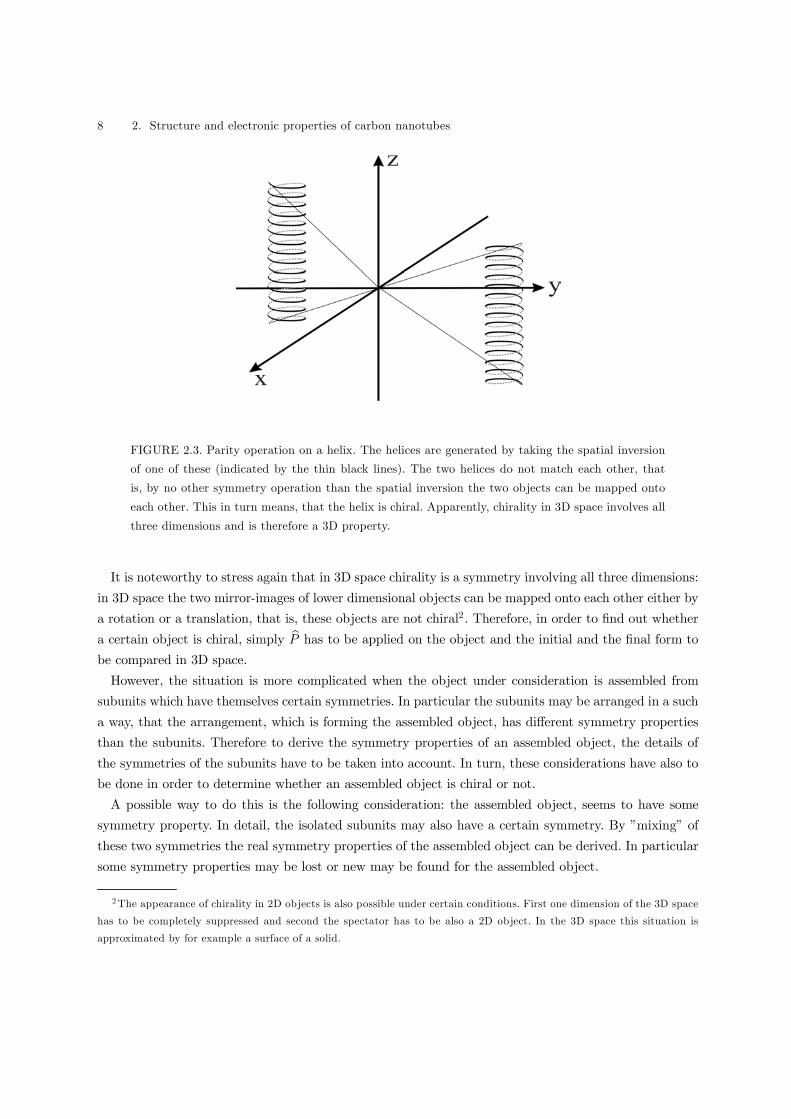
FIGURE 2.3. Parity operation on a helix. The helices are generated by taking the spatial inversion
of one of these (indicated by the thin black lines). The two helices do not match each other, that
is, by no other symmetry operation than the spatial inversion the two objects can be mapped onto
each other. This in turn means, that the helix is chiral. Apparently, chirality in 3D space involves all
three dimensions and is therefore a 3D property.
It is noteworthy to stress again that in 3D space chirality is a symmetry involving all three dimensions:
in 3D space the two mirror-images of lower dimensional objects can be mapped onto each other either by
a rotation or a translation, that is, these objects are not chiral2. Therefore, in order to find out whether
a certain object is chiral, simply bP has to be applied on the object and the initial and the final form to
be compared in 3D space.
However, the situation is more complicated when the object under consideration is assembled from
subunits which have themselves certain symmetries. In particular the subunits may be arranged in a such
a way, that the arrangement, which is forming the assembled object, has different symmetry properties
than the subunits. Therefore to derive the symmetry properties of an assembled object, the details of
the symmetries of the subunits have to be taken into account. In turn, these considerations have also to
be done in order to determine whether an assembled object is chiral or not.
A possible way to do this is the following consideration: the assembled object, seems to have some
symmetry property. In detail, the isolated subunits may also have a certain symmetry. By ”mixing” of
these two symmetries the real symmetry properties of the assembled object can be derived. In particular
some symmetry properties may be lost or new may be found for the assembled object.
2The appearance of chirality in 2D objects is also possible under certain conditions. First one dimension of the 3D space
has to be completely suppressed and second the spectator has to be also a 2D object. In the 3D space this situation is
approximated by for example a surface of a solid.

2.1 Geometric description: chirality and helicity 9
FIGURE 2.4. The parity operation transforms the chiral vector−→C n,m into -
−→C n,m. Applied to the
graphene-sheet model this implies also that the wrapping direction, up or down with respect to the
graphene-sheet plane, has to be changed in order to obtain the CNT enantiomers.
In the case of CNTs it is therefore not obvious to decide whether they and which of them are really
chiral molecular objects: both, tubular helicoidal symmetry and sixfold symmetry of the graphene lattice,
have to be taken into account. In this sense, the first symmetry represents the symmetry of the assembled
object, whereas the latter is the subunit symmetry.
First start considering the wrapping vector−→C n,m as it defines the tubular, helicoidal symmetry of a
particular CNT.−→C n,m transforms under bP as bP−→C n,m = −−→C n,m. However,
−→C n,m is defined on the basis
of the two-dimensional graphene-sheet model. Therefore a third dimension in space has to be introduced
in order to be able to describe chiral effects. The third dimension is naturally given by the wrapping-
direction perpendicular to the graphene layer: without loss of generality, +−→C n,m may define a wrapping
downwards and −−→C n,m upwards with respect to the graphene sheet plane as depicted in Fig. 2.4. That
is, in this extended graphene-sheet model,−→C n,m represents therefore three things: circumference of the
CNT, wrapping direction in and perpendicular to the graphene plane.
After extension of the two-dimensional graphene-sheet model to three dimensions, the subunit sym-
metry, that is the sixfold symmetry of the graphene lattice can be incorporated in the symmetry consid-
erations for all three classes of CNTs.
First inspect armchair CNTs like the one depicted in Fig. 2.2. Although−→C n,m and −−→C n,m in this
case point into opposite directions, there is no difference in wrapping the sheet upwards or downwards
due to the six-fold symmetry of the graphene (follow (n, n)-line in Fig. 2.1). The two resulting CNTs are
identical and thus all armchair CNTs are achiral. This is somewhat intuitive since armchair CNTs have
already no helicoidal character.
Following the same arguments and taking a view on the (n, 0)-line in Fig. 2.1 one is led to the conclusion
that also all zigzag CNTs are achiral although being helicoidal. The reason for this is the sixfold symmetry
of the graphene sheet.

10 2. Structure and electronic properties of carbon nanotubes
In contrast, the wrapping direction in the case of (n,m) CNTs, that is n 6= m 6= 0, is not affected bythe sixfold-symmetry of the graphene. The two possible forms are not identical any more and therefore
the so-termed chiral CNTs are real chiral molecular objects.
The above discussion shows, that neglecting the six-fold symmetry of the graphene lattice, the erroneous
conclusion may be drawn that all CNTs are chiral. In particular, the example of the CNTs shows that a
helicoidal character of an object is not necessarily sufficient to make the object chiral.
2.2 Conducting channels and electronic density of states
In order to describe the electronic properties of the CNTs, consider first the carbon atoms of which the
graphene-sheet lattice consists. Each carbon atom has four outer electrons sometimes termed valence
electrons. From a chemical point of view the electrons are in an orbital which is just another expression
for the probability density |ψ(−→r )|2 of the stationary eigen-wavefunction ψ(−→r ) of the electron.In the case of carbon, two of the valence electrons with opposite spin, according to Pauli’s exclusion
principle, are in the so-called s-orbital which has spherical shape. On time average each of the other two
are in one of the energy degenerated px-, py- and pz-orbital, according to Hund’s rule, which have the
shape of a rotation-symmetric dumb-bell (see Fig. 2.5).
The p-orbitals are perpendicular to each other and therefore point in each of the three spatial directions.
The angular-momentum quantum number of the s-orbital is 0 whereas the other three have the angular-
momentum quantum number 1, that is, have non-vanishing angular momentum.
In order to build up a planar graphene lattice, i.e., to form a chemical bond between the carbon atoms,
in each of the carbon atoms two of the p-orbitals (without loss of generality px- and py-orbital) hybridize
with the s-orbital to form three so-called sp2-orbitals (see Fig 2.5). These have the form of a dragged-on
rotation-symmetric dumb-bell where one half is considerably smaller than the other. The sp2-orbitals are
all arranged in one plane (in the present example the x/y-plane) and exhibit an angle of 120 between
each other and are therefore strongly oriented in space. The remaining pz-orbital is located perpendicular
to this plane. Each of the four orbitals carries now on time average one electron. Chemical bonding is
now achieved by the overlap of orbitals of neighbouring atoms as illustrated in Fig. 2.5. The neighbouring
sp2-orbitals create a strongly oriented and localized (covalent) bond whereas the pz-orbitals form a so-
called π-π-bond. The angle between the sp2-orbitals then defines the well-known honeycomb lattice of
the graphene with its sixfold symmetry.
As the binding direction of the sp2-orbitals are oriented the electrons in these orbitals are strongly
localized. In contrast, the electrons forming the π-π-bond, also termed π-electrons, are delocalized over
the entire graphene lattice. The reason for this is that each pz-orbital can principally interact (overlap)
with all its surrounding pz-orbitals from the neighbouring atoms. Systems that exhibit such delocalized
π-electrons are also called π-conjugated.
For the electronic transport in such π-conjugated systems the electrons in the sp2-orbitals are negligible
as they are strongly localized. Therefore the electronic properties of the graphene sheet (and thus of the

2.2 Conducting channels and electronic density of states 11
FIGURE 2.5. s- and p-orbitals of the carbon atom. Below to carbon atoms with three sp2-orbitals and
the remaining pz -orbital. The chemical bond is created by the overlap of neighbouring sp2-orbitals
and pz -orbitals (π-π-bonding, indicated by dotted lines.)
CNTs) are mainly determined by the π-electrons. In particular, the interaction between the pz-orbitals
on one graphene leads to (i) the delocalization of the π-electrons and (ii) the formation of energy bands
which are the bonding π-bands and the antibonding π∗-bands.
On the other hand, the relatively weak van-der-Waals interaction [13] between neighbouring graphene
layers, which is mediated by the delocalized π-electrons, results in a strong anisotropy in the electrical
conductivity of graphite: perpendicular to the graphene layers the conductivity is by a factor of 1000
smaller than the in-plane conductivity [12].
For a further description of the CNTs, periodic boundary conditions have to be introduced to the planar
two-dimensional graphene-sheet model. The boundary conditions arise naturally from the translational
symmetry along the chiral vector−→C n,m, that is along the circumference of the CNT. In view of treating
the electronic properties of a CNT with these boundary conditions it is convenient to shift to reciprocal
space.
The reciprocal lattice of a graphene layer is again a honeycomb-lattice with vectors−→b 1 and
−→b 2 which
are defined by the relation−→b i ·−→a j = 2πδij describing again a honeycomb-lattice.
A three-dimensional graph of the energy dispersion of graphene of the two lowest subbands in the first
Brioullion Zone (BZ) is given in Fig 2.6b derived by tight binding calculations [14]. The points denoted
by K are the crossing points of the π- and π∗-band. The π-band is the highest occupied energy band of
the π-electrons, whereas the π∗-band is the lowest unoccupied one. The six corresponding−→k -vectors to
the K-points in reciprocal space are
−→k K = ±
1
3
³−→b 1 −−→b 2
´, ± 1
3
³2−→b 1 +
−→b 2
´, ± 1
3
³−→b 1 + 2
−→b 2
´. (2.4)
12 2. Structure and electronic properties of carbon nanotubes
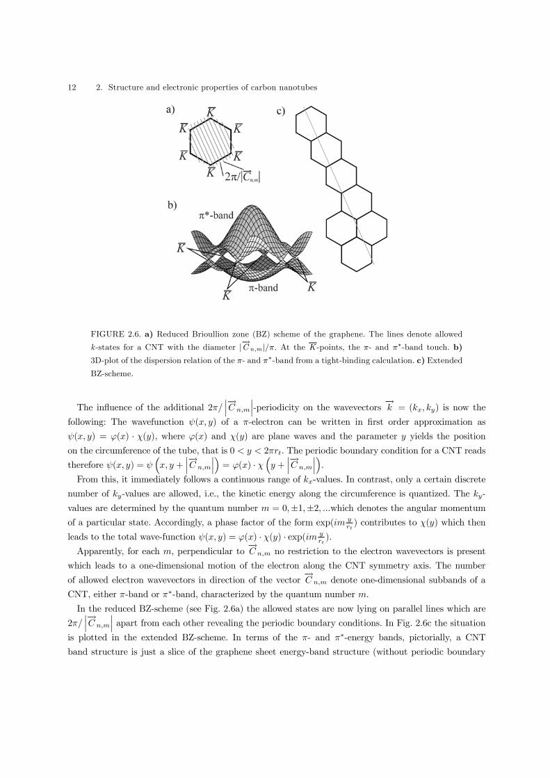
FIGURE 2.6. a) Reduced Brioullion zone (BZ) scheme of the graphene. The lines denote allowed
k -states for a CNT with the diameter |−→C n,m |/π. At the K -points, the π- and π∗-band touch. b)
3D-plot of the dispersion relation of the π- and π∗-band from a tight-binding calculation. c) Extended
BZ-scheme.
The influence of the additional 2π/¯−→C n,m
¯-periodicity on the wavevectors
−→k = (kx, ky) is now the
following: The wavefunction ψ(x, y) of a π-electron can be written in first order approximation as
ψ(x, y) = ϕ(x) · χ(y), where ϕ(x) and χ(y) are plane waves and the parameter y yields the position
on the circumference of the tube, that is 0 < y < 2πrt. The periodic boundary condition for a CNT reads
therefore ψ(x, y) = ψ³x, y +
¯−→C n,m
¯´= ϕ(x) · χ
³y +
¯−→C n,m
¯´.
From this, it immediately follows a continuous range of kx-values. In contrast, only a certain discrete
number of ky-values are allowed, i.e., the kinetic energy along the circumference is quantized. The ky-
values are determined by the quantum number m = 0,±1,±2, ...which denotes the angular momentumof a particular state. Accordingly, a phase factor of the form exp(im y
rt) contributes to χ(y) which then
leads to the total wave-function ψ(x, y) = ϕ(x) · χ(y) · exp(im yrt).
Apparently, for each m, perpendicular to−→C n,m no restriction to the electron wavevectors is present
which leads to a one-dimensional motion of the electron along the CNT symmetry axis. The number
of allowed electron wavevectors in direction of the vector−→C n,m denote one-dimensional subbands of a
CNT, either π-band or π∗-band, characterized by the quantum number m.
In the reduced BZ-scheme (see Fig. 2.6a) the allowed states are now lying on parallel lines which are
2π/¯−→C n,m
¯apart from each other revealing the periodic boundary conditions. In Fig. 2.6c the situation
is plotted in the extended BZ-scheme. In terms of the π- and π∗-energy bands, pictorially, a CNT
band structure is just a slice of the graphene sheet energy-band structure (without periodic boundary

2.2 Conducting channels and electronic density of states 13
conditions) along a certain direction. Intuitively it is clear then, that slices which cross the K-points are
describing metallic CNTs, as at these points the π- and π∗-energy band overlap. This in turn leads to
a finite density of states (DOS) at the Fermi energy EF . Other directions correspond to CNTs with a
vanishing DOS at EF , resulting in an energy-gap of typically less than 1 eV. These CNTs are therefore
semiconducting. The information whether a CNT is metallic or semiconducting can be again extracted
from the pair of integers (n,m) that has been shown to classify each CNT. Combining (2.1) and (2.4),
one can easily derive that the condition n−m = 3l (l being an integer) has to be fulfilled for a CNT to
be metallic. As a consequence, all armchair tubes are metallic whereas zigzag and chiral nanotubes can
exist as either metallic or semiconducting molecular structures.
From the previous discussion it is apparent that, in principle, electrons are only able to move along
the CNT within the subbands (one-dimensionality of CNTs) characterized by the quantum number m.
These subbands are also called conducting channels. As excitations of angular momentum states, that
is states with m 6= 0 cost a huge energy of the order 1 eV, in general all subbands with m 6= 0 can beomitted for charge transport [15]. That is, only the π- and π∗-energy bands with m = 0 contribute to the
electrical transport and, therefore, CNTs can be regarded to have just two spin-degenerated conducting
channels.
In the case of a semiconducting tube, all states in the π-band are occupied and only the π∗-band has
free states. Without doping or applying a gate-voltage or sufficiently high source-drain voltage none of
the two channels is accessible. Depending on the adjustment of these parameters, either the π- or the
π∗-band can be available for charge transport. Therefore, for these types of CNTs, solely one conducting
channel is apparent. For metallic CNTs, π- and π∗-band are crossing at the Fermi-energy, thus both
bands are able to contribute to the charge transport. Resulting in the maximum number of conducting
channels for charge transport in CNTs being two.
For the electronic density of states (DOS) of the CNTs, the strong one-dimensional character has to
be taken into account. In order to do so, consider for simplicity, a one-dimensional free electron gas
confined to the length L with infinitely high potential walls. The energy eigenvalues are given by Eν =
(~2/2m)k2ν with m the effective mass of the electrons, ~ the reduced Planck’s constant and kν = (2π/L)νthe corresponding wave-vector (ν an integer). The DOS D(E) of the system is then simply given by
D(E) =P
ν δ(E −Eν) where δ denotes the delta-distribution. In the limit of a very large system where
the number of energy eigenvalues is large and the energy difference between adjacent energies Eν is small,
D(E) can be written as
D(E) =dN
dE=
√2mL
π~E−1/2 (2.5)
where dN is the number of energy states in the energy interval dE. A factor of two for the spin-degeneracy
has been considered in the calculation. The DOS shows a divergence as the energy E approaches zero
which is known as van-Hove singularity.
The E−1/2-dependence in the DOS of CNTs could be confirmed in bandstructure calculations [16] and
experimentally with the aid of scanning tunneling microscopy. In Fig. 2.7a and 2.7b, the theoretically

14 2. Structure and electronic properties of carbon nanotubes
FIGURE 2.7. a) Calculated DOS of a (9,0) CNT [16]. At the Fermi energy (here set to zero) a finite
density of states can be found indicating that the CNT is metallic. b) DOS of a semiconducting (10,0)
CNT with vanishing density of states at the Fermi energy [16]. Note that the energy difference between
the van-Hove-singularities is considerably smaller than for the metallic CNT. For comparison, the
theoretically calculated DOS of the 2D graphene sheet is also plotted in both panels (dotted line).
c) Derivative dI/dV of the tunneling current, which is proportional to the density of states, taken
from the STM [17]. The CNTs numbered from #1-#4 are semiconducting, whereas the others are
metallic. Van-Hove singularities are apparent, confirming the theoretical considerations.
calculated DOS of a metallic (9,0) and a semiconducting (10,0) tube, respectively, is shown [16]. Several
van-Hove-singularities are visible, each of them corresponding to a certain subband of the CNT. In
Fig. 2.7c experimental spectroscopy data taken by the scanning tunneling microscope (STM) at room
temperature are depicted [17].
The figures show the differential conductance dI/dV for several SWNTs plotted versus the applied
voltage V between STM tip and the CNT under investigation. The differential conductance reflects
the (local) DOS of the CNT as the tunneling current I is proportional toR EF+eVEF
Ds(E)Dtip(E −eV ) dE where Ds(E) and Dtip(E − eV ) are the DOS of the sample at the STM tip position and the
tip, respectively [18]. Therefore, the derivative of I with respect to V yields dI/dV ∼ Ds(EF + eV ).Apparently, singularities are observed in the experimental data confirming the theoretical predictions.

3
Theoretical description and experiments to charge transport incarbon nanotubes
The unique electronic and structural properties of CNTs are also reflected in their electrical transport
properties. In this chapter, the two main characteristic features of the electrical transport through CNTs
are presented. First, it will be shown that carbon nanotubes are ballistic conductors at room temperature
which mainly originates from the absence of a strong electron-phonon coupling within the tubes. At
low temperatures, however, when the thermal energy is sufficiently small such that also low-energy
phenomena gain relevance, the electron-electron interaction becomes important. Therefore, due to its
strong 1D character CNTs are optimal candidates to exhibit Tomonaga—Luttinger-liquid-like behaviour.
Signatures in electrical transport for this behaviour were observed in SWNTs as well as MWNTs.
3.1 ballistic transport and conductance quantization
In this section the case of strongly (almost perfectly) coupled electron reservoirs to single-walled carbon
nanotubes is considered. First a introduction to ballistic conductors in terms of the Landauer-Büttiker
formalism is given. In the second part experiments, indicating that single-walled carbon nanotubes are
ballistic conductors at room-temperature, are reviewed and commented based on own considerations.
3.1.1 ballistic conductors and Landauer-Büttiker formalism
Various types of electrical transport exists. For example, charge transport processes which occur via
localized states of the charge carriers in the conductor like variable range hopping [19] or polaron hopping
[20], are known as hopping conduction. In the case, where the charges are not localized, but scattered on
dislocations, phonons or magnetic impurities (Kondo effect [21]) or even among one another along their
way in the conductor, the conduction process is called diffusive. If the charge carriers do not suffer any
scattering, the charge transport is called ballistic.
From the quantum mechanical point of view, the absence of inelastic scattering leads to the phase
preservation of the charge carrier wavefunction. Within this context the charge carriers traversing the
ballistic conductor are called phase coherent. Related to this, the so-called phase-coherence length can
be defined which is the length over which the charge carriers preserve their phase-coherence. The phase-
coherence length is not necessarily identical with the mean free path, which is the length a charge carrier
can move without being scattered. In particular elastically scattered charge carriers preserve their phase-
relationship (see Appendix A).
Diffusive conductors are known to give rise to Joule’s heating. Microscopically the heating arises from
the inelastic scattering of charge carriers in the conductor. The loss of kinetic energy is transferred to

16 3. Theoretical description and experiments to charge transport in carbon nanotubes
FIGURE 3.1. Four terminal configuration for a ballistic conductor (horizontal parallel black lines).
The voltage probes a and b are positioned on the ballistic conductor. The voltage V 0 is applied to
the reservoirs with the electrochemical potentials µ1 and µ2.
the atomic lattice of the conductor in the form of lattice vibrations (phonons) which in turn leads to
an increase of the lattice heat. Since within a ballistic conductor no mechanism to transfer energy is
available, no Joule heating is observed within such a conductor itself.
What about the resistance of a ballistic conductor? In the diffusive case the resistance arises from the
scattering of the charge carriers on the local scale. Therefore, in a four-terminal configuration, a difference
in the electrochemical potential µi between any two points a and b on the conductor is apparent. Hence,
their difference eVab = µa − µb can be observed as voltage drop. Combining Vab with the current Ithrough the conductor, the four-terminal resistance R4T ≡ Vab/I can be defined.Now, consider a four-terminal configuration as in Fig. 3.1 for a ballistic conductor. A voltage V0
is applied and two voltage-probes (a and b) are attached at arbitrary positions along the conductor.
The current through the system is Ibal. Due to the absence of scattering there is no change in the
electrochemical potential along the conductor, that is eVab = µa − µb = 0 and therefore the four-
terminal resistance yields R4T = Vab/Ibal = 0/Ibal = 0, which has also been experimentally confirmed by
measurements on a ballistic wire by de Picciotto et al. [22].
The situation is considerably different if the measurement is performed on the same device in a two-
terminal configuration. Then, the two-terminal resistance can be defined as R2T ≡ V0/Ibal. As V0 6= 0 itimmediately follows R2T 6= 0 although R4T = 0. The reason for this pretended contradiction is found inthe circumstance that in the two-terminal configuration the connecting leads and the so-called contact
resistance Rc are measured, too, to which will be referred later again.
The preceding discussion also indicates where the actual voltage drop occurs which is necessary to drive
a current through the ballistic conductor. As there is no voltage drop within the ballistic conductor, it
has to be in (or at least close to) the contacts. In turn, referring to Joule’s heating, this leads to the
heating of the contacts.
Consider now, for simplicity and without loss of generality, that a ballistic conductor is electrically
strong connected in two-terminal configuration to diffusive, infinitely large electron reservoirs. Also for
convenience, in the following, the two-terminal conductance G = R−12T is considered instead of R2T . As
in a ballistic conductor the electrons do not suffer from any scattering, the situation is analogous to

3.1 ballistic transport and conductance quantization 17
electromagnetic waves in a wave-guide. In the latter a certain number of transverse modes can propagate
the wave-guide depending on the actual shape of the wave-guide. In the case of electrical transport the
number of transverse modes, that is the contributing subbands (c.f. section 2.2), originate mainly from
the confinement of the electrons in the conductor (for a more detailed description see Appendix A). Of
course, also boundary conditions as the translational symmetry along the circumference of a CNT can
influence the number of subbands contributing to electrical transport, which was discussed in section
2.2. However, as the charge carriers are only able to move in the subbands it is intuitively clear that the
conductance G is proportional to the number Nsub of subbands available in the ballistic conductor
G = 2G0Nsub (3.1)
where the factor 2 arises from the spin-degeneracy of each subband i. The number of subbands can be
roughly estimated by the Fermi-wave-length λF of the electrons or charge carriers traversing the ballistic
conductor. The absence of scattering may be interpreted in the sense that the charges carriers do not
affect each other mutually, that is the overlap of their wavefunction is negligibly small. Thus, each charge
carrier has a certain place available which may be estimated by λF /2. If W is some characteristic width
of the ballistic conductor, then Nsub may be approximated as [23]
Nsub = int
µW
λF/2
¶, (3.2)
which could, alternatively, be also estimated utilizing the model of an electron in a box with infinitely
high potential walls.
The proportionality constant G0 can be derived in the frame of the so-termed Landauer-Büttiker
formalism [24]. Within this formalism G0 is derived (see also Appendix A) to be G0 = e2/h ≈ 38.8
µΩ−1and is called the conductance quantum. That is, each subband contributes 2G0 to the total conduc-
tance, a circumstance sometimes also termed conductance quantization. The conductance quantization
as a function of width could be shown on a ballistic wire realized by a split-gate configuration on top of
a hetero-structure [25]. Well pronounced steps of 2e2/h in the conductance were observed as the width
of the wire was increased or decreased.
However, (3.1) is only valid for perfect transmission of the incident electron wave-function into the
ballistic conductor. In the case there is a finite probability of the wave-function to be reflected from the
conductor/reservoir interface (3.1) has to be modified (c.f. Appendix A). Instead of Nsub one has to sum
over all transmission coefficients Ti which give the probability that an electron from the reservoir enters
in the subband i of the conductor. Thus (3.1) changes to
G = 2G0Xi
Ti =2e2
h
Xi
Ti. (3.4)
It is noteworthy to stress, that¡(2e2/h)
Pi Ti¢−1
is the contact resistance of a ballistic conductor
connected to two reservoirs and is sometimes misleadingly called the resistance of the ballistic conductor.
From a different point of view, the origin of this resistance is a geometrical one: the width of the ballistic
18 3. Theoretical description and experiments to charge transport in carbon nanotubes
conductor is that small that only a certain, finite number of electron modes from the reservoirs can
enter the conductor. As each electron mode can at most contribute 2e/h to the current, the conductance
quantization is naturally found.
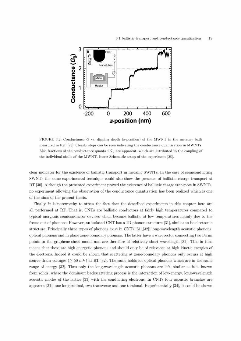
3.1.2 Experimental evidence for ballistic transport in carbon nanotubes
Several theoretical works [26],[27] suggested that CNTs are ballistic conductors showing conductance
quantization. Experimentally, in the case of MWNTs, ballistic transport and conductance quantization
at room-temperature (RT) could be shown with the aid of a STM [28]. For this, a MWNT (2.2 µm
in length, 14 nm in width) was attached to the conducting tip of an STM. The tip was connected via
a voltage source to a heatable reservoir containing mercury (Tmelting ≈ −38.84C). Thus the MWNTcould be dipped with high accuracy with respect to the horizontal direction in the liquid metal bath. In
the inset of Fig. 3.2 a schematic description of the experimental set-up is shown. A maximum voltage
of 6 V was applied, corresponding to a current density higher than 107 Acm−2 without damaging the
MWNT [28]. In comparison the current density of a typical superconductor below the critical one is of
the order 105 Acm−2 which is two orders of magnitude less. If charge transport in the MWNT is assumed
to be diffusive [28], Joule’s heating would lead to an increase of the conductor temperature up to 20000
K assuming a thermal conductivity of 10 Wcm−1K−1. This in turn would destroy the MWNT - the
typical temperature range for burning CNTs in air is around or somewhat less than 400 C. Therefore
the experimental results strongly suggest that ballistic charge transport is present, since in this case the
heat dissipates in the contacts and not in the ballistic conductor.
The conductance G of the MWNT in units of 2G0 = 2e2/h vs. the depth to which it was submerged
in the mercury is plotted in Fig. 3.2 [28]. Clearly, steps can be seen in G, yet not only of magnitude
2G0 but also fractions of it. The observation of steps as well as their heights could be attributed to
interwall interaction between the shells of a MWNT [29] when the MWNT is submerged in the mercury
at different heights. The theoretical considerations in Ref. [29] have shown that quantum conductance
channels may be blocked and/or the current traversing the MWNT redistributed nonuniformly leading
to the experimentally observed effect. Thus the presently discussed experiment strongly indicates the
existence of ballistic transport and conductance quantization in MWNTs.
In the case of SWNTs, the ballistic conductance at RT could be shown again with the aid of a scanning
probe microscope [5]. Here the microscope was used to measure the electrostatic force between a tip at
potential Vtip and a metallic SWNT connected in two-terminal configuration to metallic leads with a
small source-drain voltage applied [5]. This technique allows to measure the differences of a the local
potential on a surface. Thus, if the potential along the SWNT varies, then the electrostatic force is
changing accordingly.
In Fig. 3.3a an electrostatic force image from Ref. [5] obtained by the latter technique is shown. Clearly
no potential drop along the SWNT is observed. In the side panel (Fig. 3.3b) the electrostatic force signal
along the SWNT is shown with 100 mV applied across. The signal is flat in between the electrodes,
whereas a change is found at the contacts [5]. The absence of a potential drop along the SWNT is a
3.1 ballistic transport and conductance quantization 19
FIGURE 3.2. Conductance G vs. dipping depth (z-position) of the MWNT in the mercury bath
measured in Ref. [28]. Clearly steps can be seen indicating the conductance quantization in MWNTs.
Also fractions of the conductance quanta 2G0 are apparent, which are attributed to the coupling of
the individual shells of the MWNT. Inset: Schematic setup of the experiment [28].
clear indicator for the existence of ballistic transport in metallic SWNTs. In the case of semiconducting
SWNTs the same experimental technique could also show the presence of ballistic charge transport at
RT [30]. Although the presented experiment proved the existence of ballistic charge transport in SWNTs,
no experiment allowing the observation of the conductance quantization has been realized which is one
of the aims of the present thesis.
Finally, it is noteworthy to stress the fact that the described experiments in this chapter here are
all performed at RT. That is, CNTs are ballistic conductors at fairly high temperatures compared to
typical inorganic semiconductor devices which become ballistic at low temperatures mainly due to the
freeze out of phonons. However, an isolated CNT has a 1D phonon structure [31], similar to its electronic
structure. Principally three types of phonons exist in CNTs [31],[32]: long-wavelength acoustic phonons,
optical phonons and in plane zone-boundary phonons. The latter have a wavevector connecting two Fermi
points in the graphene-sheet model and are therefore of relatively short wavelength [32]. This in turn
means that these are high energetic phonons and should only be of relevance at high kinetic energies of
the electrons. Indeed it could be shown that scattering at zone-boundary phonons only occurs at high
source-drain voltages (≥ 50 mV) at RT [32]. The same holds for optical phonons which are in the samerange of energy [32]. Thus only the long-wavelength acoustic phonons are left, similar as it is known
from solids, where the dominant backscattering process is the interaction of low-energy, long-wavelength
acoustic modes of the lattice [33] with the conducting electrons. In CNTs four acoustic branches are
apparent [31]: one longitudinal, two transverse and one torsional. Experimentally [34], it could be shown

20 3. Theoretical description and experiments to charge transport in carbon nanotubes
FIGURE 3.3. a) Electrostatic-force image of a SWNT connected in two-terminal configuration with
an AC bias voltage of 100 mV applied to the drain electrode (dark). The source electrode is indicated
by the dotted line for clarity. The brightness of a point in the picture corresponds to a certain
electrostatic force and therefore to a certain potential at this point [5]. Apparently, the greyscale
along the SWNT is not changing indicating the absence of a potential drop. This in turn strongly
indicates the existence of ballistic transport in SWNTs. b) Trace of the potential along the SWNT
in a). The signal is flat between the electrodes, and only a potential drop in the electrodes can be
observed.
that the electron-phonon coupling of the acoustic modes is very weak, implying a scattering time of about
18 ps at RT. Assuming a typical Fermi-velocity of 8 · 105 m/s of the electrons at the Fermi-energy in aCNT, a mean free path of about 14 µm is found [34]. This length is far beyond the typical distances in
a conductance experiment and underlines the exceptional charge transport properties of CNTs.
3.2 Electron correlation at low temperatures: Tomonaga-Luttinger liquid
CNTs, in particular SWNTs, exhibit a strong one-dimensional (1D) character. The reduction of dimen-
sionality of a system from 3D to 1D has considerable consequences on its physical properties as inter-
actions as well as fluctuations gain more importance [35]. For carbon nanotubes at room temperature,
the electron-electron and electron-phonon interactions have been shown to be of minor influence on the
charge transport leading to mean free paths of about 14 µm (c.f. section 2.2) [34]. However, towards low
temperatures the electron-electron interaction becomes more relevant such that the ballistic character of
the carbon nanotubes vanishes. Instead a correlated electron state is forming, which in the low-energy
limit can be described by the so-called Tomonaga-Luttinger liquid.
In this section, first the 1D free electron gas is considered in order to exemplify the sensitivity of
1D systems to external perturbations. Then the Tomonaga-Luttinger-liquid model applied to a CNT is
presented and the main general features of the electrical transport properties are illustrated. Finally, a

3.2 Electron correlation at low temperatures: Tomonaga-Luttinger liquid 21
survey is given on transport experiments in which fingerprints of the Tomonaga-Luttinger liquid in CNTs
are found, including a discussion of the results.
3.2.1 The one-dimensional free electron system
A 1D solid may be represented by a linear chain of atoms, each of them providing one electron to the
lattice such that a 1D free electron gas is formed of length L. The 1D-topology leads to a considerable
difference in the response of the free electron gas to any kind of external perturbation, compared to 2D-
or 3D-electron systems [35]. For exemplification, consider an external, time-independent potential φ(x)
acting on the 1D free electron gas and let φ(q) be its Fourier-transform [35]. The perturbing potential
leads to a rearrangement of the electron density which may be described by an induced charge density
ρind(x).
The Fourier transform of the induced charge density ρind(q) and φ(q) are connected through the
so-called Lindhard-response function χ(q, T ) (see Fig. 3.4) [35],
ρind(q) = χ(q, T )φ(q). (3.5)
The Lindhard-response function χ(q, T ) is given by [35]
χ(q, T ) =
Z(2π)−2
f(E(k))− f(E(k + q))E(k)−E(k + q) dk (3.6)
and f(E(k)) is the Fermi-distribution. χ(q, T ) can be determined for wave-vectors q close to 2kF by
assuming a linear dispersion relation around the Fermi-energy EF , E(k)−EF = ~υF (k − kF ) [35]. Thelatter allows to readily evaluate the integral in (3.6) leading to
χ(q, T ) =
¡−e2¢π~υF
ln
¯q + 2kFq − 2kF
¯(3.7)
For q = 2kF , (3.7) has a logarithmic divergence (see Fig. 3.4) which is due to the particular topology of
the Fermi surface, also called perfect nesting of wave-vectors [35]. The most significant contribution to the
divergence arises from pairs of states, one occupied, the other unoccupied, which are 2kF apart from each
other [35]. In contrast, in higher dimensions the amount of these kinds of states is significantly reduced
such that the singularity vanishes. The behaviour of the response-function has important consequences
as can be deduced from (3.5): an external perturbation leads to divergent charge redistributions of the
1D electron system [35] and at T = 0 K the electron gas is unstable with respect to the formation of
a periodically varying electron charge density (long-range interaction) [35]. In consequence, such an 1D
electron system cannot form a stable Fermi liquid as it is known for 3D metals since the interaction
cannot be ”hidden” in the effective mass of fermionic single particles. Further, instead of single particle
excitations, only collective excitations are possible [35].

22 3. Theoretical description and experiments to charge transport in carbon nanotubes
FIGURE 3.4. Lindhard function χ(q, T ) for a 1D, 2D and 3D electron system at zero temperature
(T=0) [35]. In contrast to the 2D and 3D case, the 1D electron system exhibits a divergent response
to excitations with the wavevector 2kF . This is due to the perfect nesting property of the electronic
states in reciprocal space.
3.2.2 Tomonaga-Luttinger liquid in carbon nanotubes
It was discussed that an 1D free electron gas is unstable against any kind of perturbation such that if
electron-electron Coulomb interactions are present no Fermi-liquid state can form in which the electrons
can be still regarded as single (quasi-)particles with modified mass and/or charge [35]. The groundstate
of such an interacting 1D electron system in the absence of any scattering potentials is called a clean
Tomonaga-Luttinger or shorter Luttinger liquid (LL) [36]. The LL is characterized by a gapless collective
state whose physical correlation functions depend exponentially on the interaction strength between the
electrons [36]. The lowest excitations of the LL state are soundlike, long-wavelengths collective modes,
sometimes also called plasmon-modes [36]. These in principal propagate as any electromagnetic wave
through the system. Thus the LL formalism is a description of an interacting fermion system in the
low-energy limit [36]. From the theoretical point of view the LL-description is universal in the sense that
it does not depend on the details of the model or the interaction potential. Instead its physical properties
are only characterized by a few parameters sometimes termed critical exponents [36].
To describe electrons in a CNT in the frame of the LL theory it is easier to shift from a fermionic
to a bosonic description of the interacting electrons which is sometimes called ”bosonization” [37]. For
this, first the Hamiltonian of interacting electron system bH has to be written down in bosonized form
by introducing bosonic phase-fields θk(x) [15],[37], which are related to the local density of the electrons,
and their canonical momenta Πk(x). Four of such bosonic phase-fields are obtained by the combination of

3.2 Electron correlation at low temperatures: Tomonaga-Luttinger liquid 23
charge- and spin-degrees of freedom and symmetric and asymmetric linear combinations of the states at
the Fermi points of the 1D system [15]. The phase-fields θk(x) are denoted by the indices c+, c−, s+, s−.
The +(−) -sign denotes symmetric (asymmetric) linear combinations and c or s whether a charge- ora spin-mode is excited [15]. It is noteworthy that only the c+-mode is carrying a charge and therefore
mainly determines the electrical transport properties of the system whereas the other modes describe
neutral excitations [15]. With the aid of the phase-fields bH can now be written as [15],
bH =~υF2
Xk
Z hΠ2k + g
−2k (∂xθk)
2idx (3.8)
where the argument of the fields have been omitted for simplicity and υF is the Fermi-velocity of the
system. In this expression one can already see a particular property of the LL state, as by the introduction
of the phase-fields spin and charge are separated from each other. This, however, has no critical influence
on the further description of the electrical properties of a CNT in a LL state (see also Appendix B).
The parameter gk in (3.8) is in the case that there are no interactions present equal to 1 for all k [15].
Introducing now the Coulomb-interaction V (x− x0) which in general may also include the effects of aninsulating substrate with dielectric constant κ (κ = 1 in vacuum), an additional contribution to bH has
to be considered which is of the form [15],
bHint = 2
π
Z £∂xθc+(x)
¤V (x− x0)[∂x0 θc+(x0)] dxdx0. (3.9)
Note that as the Coulomb-interaction only acts between charged objects, only the phase-field θc+(x)
is affected. In the long-wavelength limit, that is in the low-energy limit, the bosonized description allows
to incorporate the Coulomb interaction in bH by the renormalization of gc+ [15],[37],
gc+ ≡ g =·1 +
4
π~υFV (q)
¸−1/2(3.10)
where V (q) is the Fourier transform of the Coulomb-interaction and the wave-vector q is close to zero as
the long-wavelength limit is assumed. As the Coulomb-interaction is a long-ranged interaction, V (q) has
a logarithmic singularity, requiring a infrared cutoff wavevector kcut = 2π/L [15],[38] which is determined
by the finite length L of the CNT [15]. Therefore the parameter g can be written for CNTs as
g =
·1 +
8e2
πκ~υFln
µL
2πrt
¶¸−1/2(3.11)
where rt is the radius of the tube. It is noteworthy that although the phase-fields θk 6=c+(x) are not affected
by the Coulomb-interaction, the parameters gk 6=c+ are also suffering from a tiny renormalization as the
bosonic fields are by construction to some degree entangled (c.f. Appendix B). However, the corrections
are << 1 such that only at temperatures T ≈ 0.1 mK these would start to have an influence [15], whichis far below the temperatures used in the experimental part of the present thesis.
From (3.11) it is apparent that g incorporates the interaction between the electrons in the CNT and
is therefore a direct measure of the interaction strength. Thus g is also called interaction parameter
24 3. Theoretical description and experiments to charge transport in carbon nanotubes
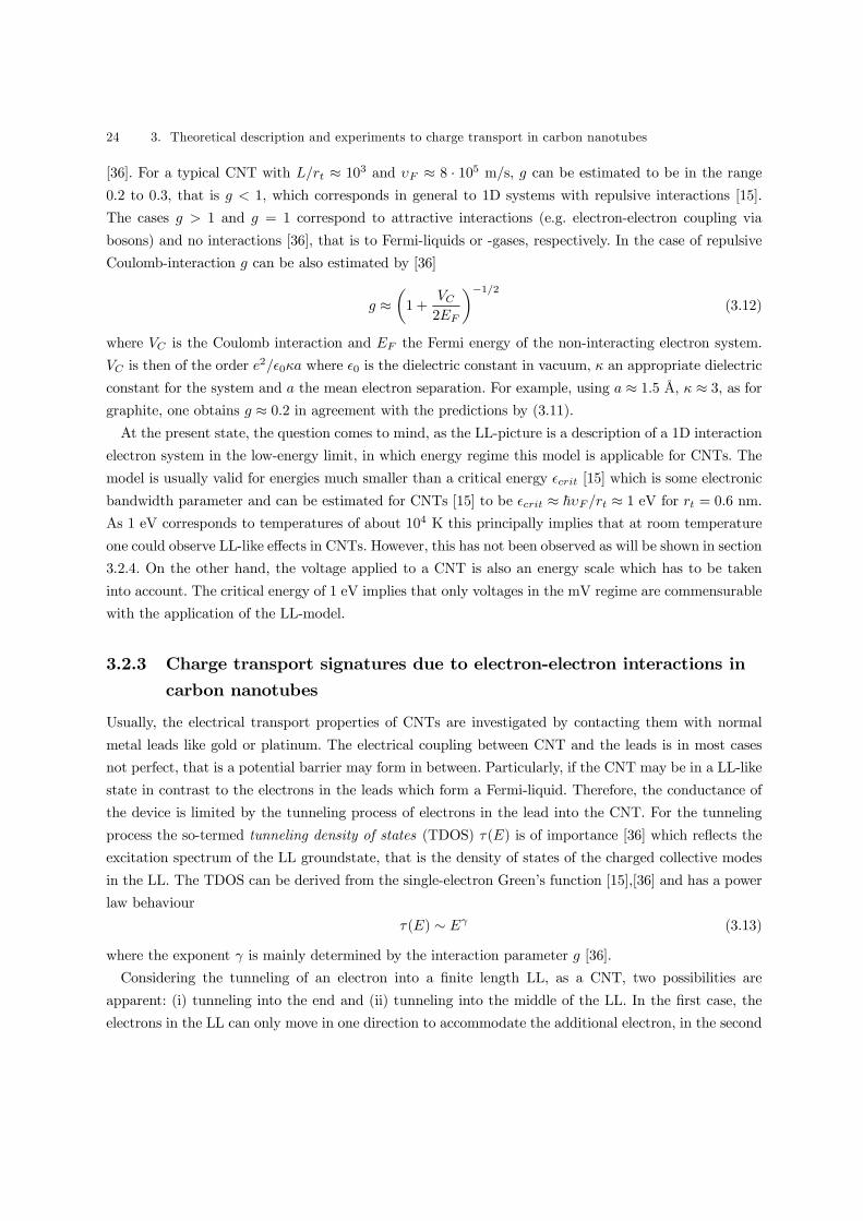
[36]. For a typical CNT with L/rt ≈ 103 and υF ≈ 8 · 105 m/s, g can be estimated to be in the range0.2 to 0.3, that is g < 1, which corresponds in general to 1D systems with repulsive interactions [15].
The cases g > 1 and g = 1 correspond to attractive interactions (e.g. electron-electron coupling via
bosons) and no interactions [36], that is to Fermi-liquids or -gases, respectively. In the case of repulsive
Coulomb-interaction g can be also estimated by [36]
g ≈µ1 +
VC2EF
¶−1/2(3.12)
where VC is the Coulomb interaction and EF the Fermi energy of the non-interacting electron system.
VC is then of the order e2/²0κa where ²0 is the dielectric constant in vacuum, κ an appropriate dielectric
constant for the system and a the mean electron separation. For example, using a ≈ 1.5 Å, κ ≈ 3, as forgraphite, one obtains g ≈ 0.2 in agreement with the predictions by (3.11).At the present state, the question comes to mind, as the LL-picture is a description of a 1D interaction
electron system in the low-energy limit, in which energy regime this model is applicable for CNTs. The
model is usually valid for energies much smaller than a critical energy ²crit [15] which is some electronic
bandwidth parameter and can be estimated for CNTs [15] to be ²crit ≈ ~υF/rt ≈ 1 eV for rt = 0.6 nm.As 1 eV corresponds to temperatures of about 104 K this principally implies that at room temperature
one could observe LL-like effects in CNTs. However, this has not been observed as will be shown in section
3.2.4. On the other hand, the voltage applied to a CNT is also an energy scale which has to be taken
into account. The critical energy of 1 eV implies that only voltages in the mV regime are commensurable
with the application of the LL-model.
3.2.3 Charge transport signatures due to electron-electron interactions incarbon nanotubes
Usually, the electrical transport properties of CNTs are investigated by contacting them with normal
metal leads like gold or platinum. The electrical coupling between CNT and the leads is in most cases
not perfect, that is a potential barrier may form in between. Particularly, if the CNT may be in a LL-like
state in contrast to the electrons in the leads which form a Fermi-liquid. Therefore, the conductance of
the device is limited by the tunneling process of electrons in the lead into the CNT. For the tunneling
process the so-termed tunneling density of states (TDOS) τ(E) is of importance [36] which reflects the
excitation spectrum of the LL groundstate, that is the density of states of the charged collective modes
in the LL. The TDOS can be derived from the single-electron Green’s function [15],[36] and has a power
law behaviour
τ(E) ∼ Eγ (3.13)
where the exponent γ is mainly determined by the interaction parameter g [36].
Considering the tunneling of an electron into a finite length LL, as a CNT, two possibilities are
apparent: (i) tunneling into the end and (ii) tunneling into the middle of the LL. In the first case, the
electrons in the LL can only move in one direction to accommodate the additional electron, in the second

3.2 Electron correlation at low temperatures: Tomonaga-Luttinger liquid 25
FIGURE 3.5. τ (E ) for g = 0.28 and g = 0.75 corresponding to tunneling in the middle and in the
end, respectively, of a CNT in a LL-state. Both curves are vanishing as E = 0 is approached.
case they can move into two directions. This leads to a difference in the exponent γ [15] depending at
which position of the LL the tunneling event occurs
γmid =¡g + g−1 − 2¢ /8 (3.14)
γend =¡g−1 − 1¢ /4 .
Apparently, γend > γmid in general for repulsive interactions. In the case of a Fermi-liquid, that is
g = 1, γend = γmid = 0 and therefore τ(E) = const. For g ≈ 0.25, which would be a typical value for aCNT one finds γmid ≈ 0.28 and γend ≈ 0.75. The corresponding TDOS τmid(E) and τend(E) are plottedin Fig. 3.5. It is noteworthy that the introduction of strong (high energy barrier) or weak (low energy
barrier) scatterers [36] in the LL resembles the same behaviour as tunneling into the end or the middle,
respectively, of a LL [36]. The strong scatterer, in contrast to the weak scatterer, ”cuts” the LL into two
distinct parts, which then in the sense of electrical transport leads to tunneling into the end of a LL
when passing the scatterer [36].
As the TDOS describes the available states in which an electron can tunnel into the LL it is intuitively
clear that the conductance G(E) of this device is proportional to τ(E) and has therefore the same energy
dependence, that is G(E) ∼ Eγ . Experimentally, the energy E is tuned via the applied voltage V . In
a more rigorous theoretical treatment [36],[38] also the temperature dependency and the dependence of
the current on the applied voltage can be derived, leading to
G(V ) ∼ V γ (3.15)
G(T ) ∼ T γ
I(V ) ∼ V γ

26 3. Theoretical description and experiments to charge transport in carbon nanotubes
where for the exponent γ either γend or γmid has to be taken depending on the actual experimental
configuration.
The discussion here obviously shows that the way how and ”where” a CNT is electrically contacted
is a crucial (geometric) parameter for electrical transport measurements and should therefore be always
considered for interpretation of the experimental data.
3.2.4 Experimental fingerprints of the Tomonaga-Luttinger liquid in carbon
nanotubes
Experimental indications for the LL state was found in both, MWNTs [39] as well as SWNTs [6]. In the
case of MWNTs, the differential conductance dI/dV was measured as function of source-drain voltage
V and temperature T (Fig. 3.6) [39]. The MWNT investigated was connected from top with electrodes
(up-left inset Fig. 3.6). In this experiment reported in Ref. [39] the contact to which bias was applied was
high-ohmic (about 300 kΩ), implying a high tunneling barrier, although the metal and the MWNT are
in intimate contact. Local defects in the MWNT, orientation differences of the metal grains and similar
effects may be reasons for this.
FIGURE 3.6. Conductance vs. source-drain voltage of a MWNT in two terminal configuration mea-
sured (upper left inset) for different temperatures [39]. The decrease of the conductance around zero
bias voltage is attributed to the tunneling density of states τ(E) of the MWNT which implies the
existence of a Luttinger-liquid-like electron state. This phenomenon is termed zero-bias anomaly.
lower right inset: temperature dependence of the zero-bias anomaly in a log/log-scale. A straight line
with the slope 0.36 can be extracted. The dotted line in the main figure is a theoretical fit with G ∼V 0.36.

3.2 Electron correlation at low temperatures: Tomonaga-Luttinger liquid 27
However, as the TDOS is proportional to dI/dV , the measurements shown in Fig. 3.6 are a direct
measure of the first one. The dotted line is a theoretical fit [39]: dI/dV ∼ V 0.36 and the value of
the exponent was drawn from the temperature dependence of the differential conductance [39] (down-
right inset Fig. 3.6) at zero source-drain voltage. Theoretical fit and experimental data at 2 K show
a good agreement indicating the existence of the LL-state in MWNTs. The decrease of the differential
conductance in the vicinity of the zero source-drain voltage is termed zero-bias anomaly (ZBA) [39] and is
attributed to the power-law dependence in energy of the TDOS, which is one of the main characteristics
of a LL.
As the contacting configuration in the experiment reported in Ref. [39] is middle-contacted, the inter-
action parameter can be extracted to be about 0.22 from the data shown in Fig. 3.6 which is in good
agreement with the theoretical predicted range of values in the previous sections. However, although
the results are indicating a LL state in MWNTs, other measurements [7],[40] point towards a diffusive
type of transport. Indeed theoretical considerations on disordered (non-LL) multi-channel wires [41] show
also a ZBA. Additionally, calculations including shell-shell interactions in MWNTs [42] may be also of
importance. Therefore at the present state it is not clear whether MWNTs really represent a LL-like
electron system.
Turn now to the experiments on SWNTs [6]. In Ref. [6] metallic SWNTs have been contacted in two
ways: (i) electrodes are deposited on top and (ii) SWNTs are adsorbed on in SiO2-buried metal electrodes.
In the first case the two-terminal resistance at room-temperature is relatively low (. 30 kΩ) and in thesecond higher (& 67 kΩ) [6]. In Fig. 3.7 the differential conductance vs. the temperature is plotted in alog-log-scale for the two types of devices, showing again a power-law dependence [6].
The left graph corresponds to SWNTs on top of electrodes, the right one to SWNTs buried under
electrodes. The respective exponents can be extracted from the slope of the curves in Fig. 3.7, γtop ≈0.3 and γunder ≈ 0.6 [6]. Apparently, the two values differ significantly, yet the interaction strength
(parameter) should be roughly the same for each SWNT and both samples can be regarded as middle-
contacted as illustrated in the insets of Fig. 3.7. In order to clarify the situation, refer to the comment
in section 3.2.3, stating that the two limits, end- and middle-tunneling can also be achieved via the
introduction of weak and strong scatterers [36] in the LL.
Consider first the case, when the SWNTs are lying on top of electrodes. Obviously, as can be drawn
from the room-temperature two-terminal resistance, the coupling between metal and SWNT is relatively
small, such that only a weak perturbation on the electronic system of the SWNT can be expected. This
situation maps with the case of a weak scatterer in a LL and therefore γtop = γmid =¡g + g−1 − 2¢/8.
The situation is different for the SWNTs lying under the electrodes. The metal and the SWNT are in
much more intimate contact then in the other case. Therefore the electron system in the SWNT should
be considerably perturbed in contrast to a electrically weak coupling. If the perturbation is strong enough
then the sensitive LL-state in the SWNT can be locally lifted in the sense of ”cutting” the electron system
into pieces. This in turn would lead to an end-tunneling-like configuration, although the electrodes are
placed in the middle of the SWNT and thus γunder = γend =¡g−1ρ − 1
¢/4. Extracting from the SWNT
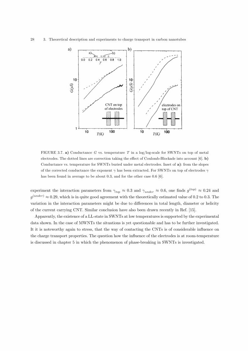
28 3. Theoretical description and experiments to charge transport in carbon nanotubes
FIGURE 3.7. a) Conductance G vs. temperature T in a log/log-scale for SWNTs on top of metal
electrodes. The dotted lines are correction taking the effect of Coulomb-Blockade into account [6]. b)
Conductance vs. temperature for SWNTs buried under metal electrodes. Inset of a): from the slopes
of the corrected conductance the exponent γ has been extracted. For SWNTs on top of electrodes γ
has been found in average to be about 0.3, and for the other case 0.6 [6].
experiment the interaction parameters from γtop ≈ 0.3 and γunder ≈ 0.6, one finds g(top) ≈ 0.24 andg(under) ≈ 0.29, which is in quite good agreement with the theoretically estimated value of 0.2 to 0.3. Thevariation in the interaction parameters might be due to differences in total length, diameter or helicity
of the current carrying CNT. Similar conclusion have also been drawn recently in Ref. [15].
Apparently, the existence of a LL-state in SWNTs at low temperatures is supported by the experimental
data shown. In the case of MWNTs the situations is yet questionable and has to be further investigated.
It it is noteworthy again to stress, that the way of contacting the CNTs is of considerable influence on
the charge transport properties. The question how the influence of the electrodes is at room-temperature
is discussed in chapter 5 in which the phenomenon of phase-breaking in SWNTs is investigated.
4
Sample preparation
In this chapter the contacting of SWNTs by metal electrodes is described. For this, at first SWNT raw-
material has to be purified which is described in the first section of this chapter. Then conventional
electron-beam lithography is used to pattern an electrode structure. As contacting material gold (Au)
and gold palladium (AuPd), the superconductors lead (Pb), indium (In), aluminium (Al) and rhenium
(Re) and the ferromagnetic cobalt (Co) have been investigated. In addition the alloy gold germanium
(AuGe) and an approach utilizing azido-molecules have been tried.
With the experimental set-up described in the third section, the two-terminal resistance of all of these
samples contacting SWNTs is measured which is indicative for the electrical coupling between SWNT
and metal.
In view of the requirements of the experiments in the present thesis, the noble alloy AuPd and the
superconductor Re, both contacting SWNTs from top, were found to be the optimum choice of contacting
material and way of contacting.
4.1 Purification of carbon nanotubes and adsorption on substrates: surfacetreatment
CNTs can be produced by various methods. Historically, at first the arc-discharge method [43] was used.
Herein, a voltage is applied between two graphitic rods in a closed volume. The ends are then successively
drawn nearer until the electric field is high enough to ignite a plasma. After several minutes a black,
fibrous soot can be found within the device containing CNT material. The method described so far only
produces MWNTs. If in addition small amounts of catalyst, e.g. yttrium, nickel or iron, are provided
within the graphitic rods, SWNTs also can be obtained.
In contrast to the arc-discharge method, the laser-ablation method [44] is restricted to a smaller reaction
area (diameter of laser beam . 1 µm). A laser beam is pointed onto a piece of bulk graphite which itselfis in a relatively long (quartz) tube. At the other end of the tube a (sometimes cooled) metal rod is
inserted. Due to the temperature gradient between the bulk graphite and the metal rod, the produced
particles diffuse to and disengage at the latter. Again, a black soot containing MWNTs is found, yet
not as fibrous as in the case of the arc-discharge method. Analogously, addition of catalyst allows the
production of SWNTs.
Another method is based on the catalytic decomposition of molecules in gas phase like acetylene [45].
A bulk catalyst is placed in the middle of a quartz tube which itself again is placed in a furnace. The
gas of the molecules to be decomposed is flowing continuously through the quartz tube leaving a black
powder on the catalyst. Depending on the catalyst used, and also the size of the catalyst particle, either
MWNT or SWNT material can be produced. In the first case, the MWNTs are not as well graphitized

30 4. Sample preparation
as obtained by other methods. In contrast, the SWNTs seem to contain less defects relative to the other
SWNTs materials but only small quantities are obtained.
A more recent method utilizes the reaction of gaseous CO with a catalyst precursor [46]. Hot and cold
CO is mixed together in the presence of the catalyst, here Fe. The process is performed at approximately
900C and yields SWNTs and CO2-gas. In contrast to the previous methods an extension to large scale
production of CNTs is possible, since there is no principle restriction to space for the reaction to take
place and the product is relatively pure with respect to undesired side-products. On the other hand, a
MWNT production is not achieved with this process.
All of the shortly described production methods provide raw material consisting of MWNTs or SWNTs
and other forms of carbon: fullerenes, graphite and amorphous carbon. The composition of the raw-
material varies depending on production method and the growth parameters employed (temperature,
catalyst, pressure,...) during the production process. However in all processes, except for the catalytic-
decomposition-process, undesired side-products are contained in the raw-material.
In the present thesis mainly SWNT raw-material obtained by the arc-discharge and the laser-ablation
method has been used. Therefore purification of the raw-material is necessary in order to get access
to individual or thin bundles of SWNTs. For this, the methods described in references [47] and [48]
are followed. The basic idea of these approaches is to disperse the raw-material in an aqueous solution
containing surfactant. The surfactant molecules form a shell called micelle around the particles in the
raw-material allowing them to form a stable dispersion. The principle is depicted in Fig. 4.1a.
FIGURE 4.1. a) Schematic view of a SWNT and a particle enclosed by a surfactant shell (micelle).
The surfactant has negatively charged headgroups. The molecular structure of the surfactant is
depicted on the right. b) Silanization process of a SiO2 surface. After silanization, the negatively
charged micelle and the positively charged amino groups attract each other, promoting the adsorbtion
on the surface.

4.1 Purification of carbon nanotubes and adsorption on substrates: surface treatment 31
FIGURE 4.2. Scanning force microscopy image of SWNTs and SWNT bundles adsorbed from a
purified surfactant-stabilized aqueous dispersion onto a silanized SiO2 surface.
In order to obtain a dispersion, SWNT raw-material produced by the arc-discharge or laser-ablation
method was used containing approximately 40 to 60% SWNTs. About 0.2 mg of the raw-material was
added to 275 µl of an aqueous 1 wt% lithium dodecyl sulfate (LDS; purchased from Fluka) solution
and then subjected to ultrasonic agitation for 2 min (KLN-Ultraschall-Generator 281/101). During this
treatment, the entangled SWNT-network is disintegrated into SWNT bundles and individual SWNTs,
which are surrounded by a surfactant shell. LDS mainly consists of a negatively charged ionic headgroup
and a hydrophobic tail (see Fig. 4.1a), such that the micelle surrounding the SWNT, or other particle is
negatively charged. Thus prepared dispersions are stable for several days. Centrifugation of the disper-
sions for 30 min at 8000 rpm (Eppendorf - Centrifuge 5417 C) was performed in order to collect larger
aggregates in the sediment. The supernatant is then removed and stored into another vessel.
In order to obtain information as to whether the purification process was successful, particles are
adsorbed from the supernatant onto a substrate and then investigated by scanning force microscopy.
A silicon (Si)-wafer with thermally grown SiO2 layer is used as substrate. For adsorption on the SiO2surface, the negatively charged micelle is utilized. By silanization, the OH-groups of the SiO2 surface are
exchanged by ammonium-groups (see Fig. 4.1b) which exhibit a positive charge in protonic (i.e. containing
H+ ions) solvents. Thus, a droplet of aqueous supernatant leads to a positively charged surface and
the electrostatic interaction with the negatively charged micelle promotes the adsorption. Mainly three
silanes have been used, 3-aminopropyltriethoxysilane, N-[3-(Trimethoxysilyl)propyl]-ethylenediamine and
3-aminopropyldimethyl-ethoxysilane. During the studies, no qualitative or quantitative difference could
be found for these three silanes with respect to the adsorption of particles. The silanization procedure
can be generalized as follows: the substrate is first cleaned successively 10 min in acetone and 10 min in
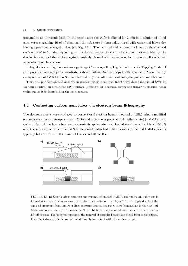
32 4. Sample preparation
propanol in an ultrasonic bath. In the second step the wafer is dipped for 2 min in a solution of 10 ml
pure water containing 10 µl of silane and the substrate is thoroughly rinsed with water and blown dry
leaving a positively charged surface (see Fig. 4.1b). Then, a droplet of supernatant is put on the silanized
surface for 20 to 30 min, depending on the desired degree of density of adsorbed particles. Finally, the
droplet is dried and the surface again intensively cleaned with water in order to remove all surfactant
molecules from the surface.
In Fig. 4.2 a scanning force microscopy image (Nanoscope IIIa, Digital Instruments, Tapping Mode) of
an representative as-prepared substrate is shown (silane: 3-aminopropyltriethoxysilane). Predominantly
clean, individual SWNTs, SWNT bundles and only a small number of catalytic particles are observed.
Thus, the purification and adsorption process yields clean and (relatively) dense individual SWNTs
(or thin bundles) on a modified SiO2 surface, sufficient for electrical contacting using the electron beam
technique as it is described in the next section.
4.2 Contacting carbon nanotubes via electron beam lithography
The electrode arrays were produced by conventional electron beam lithography (EBL) using a modified
scanning electron microscope (Hitachi 2300) and a two-layer poly(methyl methacrylate) (PMMA) resist
system. Each of the layers has been successively spin-coated and heated (each layer for 1 h at 160C)
onto the substrate on which the SWNTs are already adsorbed. The thickness of the first PMMA layer is
typically between 75 to 100 nm and of the second 40 to 80 nm.
FIGURE 4.3. a) Sample after exposure and removal of cracked PMMA molecules. An under-cut is
formed since layer 1 is more sensitive to electron irradiation than layer 2. b) Principle sketch of the
exposed structure from top. Four lines converge into an inner structure (dimensions in the text). c)
Metal evaporated on top of the sample. The tube is partially covered with metal. d) Sample after
lift-off process. The undercut promotes the removal of undesired resist and metal from the substrate.
Only the tube and the deposited metal directly in contact with the surface remain.
4.3 Experimental set-up for electrical transport measurements 33
The first layer is more sensitive with respect to the irradiation of electrons. Thus, in the lower layer more
PMMA-molecules are cracked than in the second layer during the exposure process. After exposure, the
cracked PMMA molecules are removed with a solution consisting of 15 ml isopropanol and 5 ml isobutyl-
methylketone leading to a so-called under-cut (see Fig. 4.3a) resulting from the different sensitivities of
the two PMMA layers used.
The electrode geometry used in order to contact the SWNTs (see Fig. 4.3b) consist of four lines,
converging in an inner finger-structure, each of them 2 µl long, about 100 nm wide and approximately
100 to 200 nm apart. These dimensions are sufficiently small to contact the SWNTs which have been
adsorbed previously.
In the next step, metal is evaporated on top of the sample under vacuum (p . 1 ·10−6 to 1 ·10−9 mbar,see section 4.4), resulting in the SWNTs being electrically contacted on top (see Fig. 4.3c). The evapora-
tion rate varies from metal to metal. In the case of a non-noble metal being evaporated, the rate is usually
higher (about 7 to 10 Å/sec) in order to avoid contaminations picked up on the way from evaporation
source to substrate. As the vacuum is never completely clean, small amounts of water, hydrocarbons
and other gases are present. Noble metals are much less sensitive to this type of contamination, allowing
considerably lower evaporation rates (about 1 Å/sec).
Finally, the undesired metal and PMMA is removed during the lift-off process. For this, the substrate
is submerged for 2 h in an acetone bath at approximately 55C. Afterwards, the sample is thoroughly
rinsed in acetone and isopropanol and blown dry (see Fig. 4.3d) leaving only the metal which is in
direct contact with the substrate’s surface and the SWNTs. Note that in Fig. 4.3c an idealized picture is
shown. In reality still connections between the metal film on top of the PMMA layers and the metal on
the substrate are found. This can lead to residues of metal on the electrodes and the substrate surface
if the lift-off process has not optimally occurred. In particular, the more ductile a metal is, the more
difficult the lift-off process is. This is also the case when the thickness of the evaporated metal increases
with respect to the total PMMA-layer thickness.
4.3 Experimental set-up for electrical transport measurements
The electrical transport measurements in the present thesis have been performed on two cooling systems:
a simple liquid 4He bath for measurements down to 4.2 K and a 3He/4He dilution refrigerator (TLM
400, Oxford Instruments) which has a minimum base temperature around 25 mK. The latter system is
of particular necessity for samples in which SWNTs have been contacted with superconducting electrode
materials (c.f. chapter 6).
In both cases the principle experimental set-up was the same as it is depicted in Fig. 4.4. The main
components of the system consist of a voltage adder, a voltage divider and a current-voltage converter
(Ithaco 1211). High- and low-pass filters have also been used in order to avoid undesired frequency signals
from voltage sources or the environment.

34 4. Sample preparation
FIGURE 4.4. Principle experimental set-up for electrical transport measurements. The main elements
of the set-up are denoted in the figure. Their principal function is given in the text.
In the case of the liquid 4He bath, the electrical reference point ”ground” was defined by the pump that
was used to evacuate the sample storage space. In the other system, the 3He/4He dilution refrigerator has
been appropriately connected to ground. All devices in the set-up are disconnected from each other and
the external power supply via transformators such that no ”ground—to-ground” slope has been possible.
The current-voltage converter was used as its input is at constant potential and thus allowing an
accurate measurement of the current Isd. In addition effects resulting from a possible non-linear behaviour
of measurement devices are diminished. The output signal Voutput of the current-voltage converter is given
in V. In particular the conversion factor µ of Isd into a voltage can be varied. For example, consider a
current Isd ∼ 10−9 A passing through the sample. If µ = 10−8 A/V is chosen then the output voltage
is Voutput = Isd/µ ∼ 10−1 V. That is, instead of measuring a current in the nA range, a voltage of somehundreds of mV is measured.
The voltage adder is used in order to reduce offset voltages from the current-voltage converter. For
this, an additional voltage source Vadd was connected to the voltage adder which is already connected to
the source-drain-voltage source Vsd.
The voltage divider (1:10 to 1:1000) was mainly used to protect the sample from accidently occurring
high voltage peaks, to some extent reducing noise and to minimize the fluctuations of Vsd which can in
particular occur in long term measurements.
As indicated in Fig. 4.4, the whole experimental set-up is outside the cooling system, such that prin-
cipally it can be exchanged or modified without altering the sample. In order to electrically protect the
sample during changes in the set-up and during introduction and removal of the sample in and out of the
cooling system, all electrodes are grounded simultaneously. Thus, no electrical pulse or electrostatic fluc-
tuation can lead to the destruction of the sample. This electrical shielding turned out to be particularly
vital for the SWNT-samples investigated in the present thesis.

4.4 Increase of electrical coupling between metal and SWNT: room temperature measurements 35
4.4 Increase of electrical coupling between metal and SWNT: room
temperature measurements
Experimental studies in order to find the most suitable metal for a strong electrical coupling to the
SWNT, that is, minimization of the contact resistance between metal and SWNT, are presented in this
section. Various metals as contacting materials as well as different approaches for contacting are described.
The topology of the samples is investigated utilizing scanning force microscopy (SFM) and the electrical
coupling is tested by measuring the two-terminal room-temperature resistance of a contacted SWNT.
4.4.1 Testing different metals
In this section different metals have been used to electrically contact SWNTs adsorbed in a previous
step on a substrate. Two-terminal current/voltage characteristics of these structures are presented and
several reasons for the observed electrical behaviour are suggested.
Noble metals: Au and AuPd
The easiest metals to handle are noble metals: they do not oxidize in air, can be easily evaporated (in
most cases) and are chemically stable. Thus, the first metals that have been used to electrically contact
FIGURE 4.5. SFM image of a Au electrode structure on a 3-aminopropyltriethoxysilane treated
SiO2 surface. The adhesion of the Au to the surface is sufficiently strong due to the silanization. The
particles in between and around the electrodes are lift-off residues. Their presence indicates also the
affinity of the Au to the silanized surface.

36 4. Sample preparation
FIGURE 4.6. Au-electrode structure with one completely detached electrode. Some residues allow to
observe the contour of the former position where the electrode has been. Before detachment a SWNT
bundle has been buried under it. The image illustrates that the adhesion of SWNTs to the silanized
surface is of similar strength or stronger than the adhesion of Au (for AuPd similar observations have
been done) to this surfaces.
CNTs are Au [49] and platinum [4]. In the present thesis Au and AuPd (40 wt%/ 60 wt%) have been
chosen to contact SWNTs for charge transport measurements. AuPd has the advantage that its grain
size (2 to 3 nm) is about half of that of Au leading to a smother surface when evaporated on a substrate.
Later, it is shown that this also has an influence on the lift-off process.
As substrates commercially available n+-doped Si (dopant: arsenic) were used with a thermally grown
SiO2 surface (thickness: 100 nm) on which the SWNTs are adsorbed. The highly doped Si can therefore be
used as a backgate in the measurements. The samples have been produced in the way previously described
in sections 4.1 and 4.2 where 3-aminopropyltriethoxysilane has been used as silane. The evaporation has
been carried out at p . 1 · 10−6 mbar and metal-deposition rates of 1 Å/s for both Au and AuPd wereused.
Fig. 4.5 shows a typical SFM image Au-electrode structure for contacting SWNTs. The electrode lines
are about 24 nm in height, 2 µm in length (inner structure) and the distance between two neighbouring
lines is approximately 150 nm. On the substrate only some smaller particles (most probably catalyst)
are observed. Between the electrode lines more particles are found which are residues from the lift-off
process. It is remarkable that the adhesion of Au to the SiO2 surface is sufficiently strong. Usually Au
has only a poor adhesion to SiO2 such that it is removed during the lift-off process. To overcome this
problem, titanium (Ti) or chromium (Cr) is used as an adhesion promoter. In this case, a thin Ti or Cr

4.4 Increase of electrical coupling between metal and SWNT: room temperature measurements 37
layer (3 to 5 nm’s usually) is evaporated before the final Au layer. However, Fig. 4.5 demonstrates that
the silanized SiO2 surface leads to a sufficiently strong adhesion of Au such that the lift-off process can
be performed.
Occasionally, partially detached electrode lines are observed (see Fig. 4.6) after lift-off, indicating that
the adhesion of SWNTs on the silanized SiO2 surface is of similar strength or stronger than the adhesion
of Au to this surface. During the experiments it was found that the amount of detached electrode lines
increases the longer the time between adsorbtion and spin-coating is. Presumably, the silanization of the
SiO2 surface is passivated when exposed to air for long periods, leading to these observations. By closer
inspection of the outer right hand electrode in Fig. 4.7, the contour of the SWNT buried under the metal
seems to press through the metal. This indicates that the structural integrity of the SWNTs does not
suffer from the evaporation process.
Fig. 4.7 shows an electrode array connecting several SWNTs, using AuPd (15 nm thickness) instead
of Au as the evaporation material. In the area between the electrodes considerably less particles are
observed than in the case of Au and also the edges of the electrode lines are smoother. Since the grain
size of AuPd (about 20 Å) is smaller than the one of Au (about 40 Å) and it is less ductile, the lift-off
process is easier to perform (c.f. section 4.2) and no residues are apparent.
FIGURE 4.7. AuPd-electrodes connecting two (presumably) individual SWNTs (electrode pair (I))
and a thin bundle (. 3 nm in height; electrode pair (II)). The SWNTs connected by electrode pair
(I) are denoted by arrows. The contour of the SWNTs clearly presses through the metal.

38 4. Sample preparation
FIGURE 4.8. a) I/V -characteristic of electrode pair (I) in Fig. 4.7. The resistance of the two
in parallel contacted SWNTs is approximately 50 kΩ. Current fluctuations are observable at
higher source-drain voltages which are attributed to thermal instabilities of the contact region. b)
I/V -characteristic of electrode pair (II). The curve is over the same voltage range, almost free of
fluctuations and the resistance is only 10 kΩ.
Electrode pair (I) is connected through two (presumably) single SWNTs (indicated by arrows) whereas
electrode pair (II) electrically connects a thin bundle (diameter . 3 nm). Interestingly, the contour of
the SWNTs and the SWNT bundle is clearly observable in the metal profile. Thus, as in the case of Au
already suggested, the structural integrity of the SWNTs is preserved during the evaporation process.
Electrical transport measurements at room temperature in helium atmosphere of the sample in Fig.
4.7 are depicted in Fig. 4.8. In Fig. 4.8a the data for electrode pair (I) is shown. The resistance of the
two in parallel contacted SWNTs is approximately 50 kΩ > h/2e2 and at higher source-drain voltage,
current fluctuations are observable. Assuming that both SWNTs carry the same amount of current, each
of them has a two-terminal resistance of about 100 kΩ, indicating that at lower temperatures, single-
electron effects may be observable. In contrast the room-temperature resistance of electrode pair (II)
(Fig. 4.8b) is only about 10 kΩ. This quite close to the theoretically expected value of h/4e2 ≈ 6.45 kΩfor a metallic SWNT (c.f. section 3.2), in case of ballistic transport (c.f. chapter 5). In addition, compared
to the current/voltage (I/V ) -characteristic of electrode pair (I), no current fluctuations occur at higher
source drain voltages. The fluctuations are therefore attributed to thermal instabilities of the contact
region.
The electrical room-temperature properties in the present sample are representative for all samples
contacted with AuPd or Au: some SWNTs exhibit very low (. 10 kΩ) two-terminal resistances, othersup to a few hundreds of kΩ. Several reasons are to be considered for this observed behaviour:
(i) In the case of low resistances, a metallic SWNT is electrically coupled well to the leads, such that
the transmission coefficient between lead and SWNT is almost unity. Then the two-terminal resistance
is comparable with the lowest possible value of h/4e2 ≈ 6.45 kΩ. If the two-terminal resistance is a fewhundreds of kΩ, then a semiconducting SWNT may be contacted. In this case a Schottky barrier would

4.4 Increase of electrical coupling between metal and SWNT: room temperature measurements 39
form at the interface where semiconducting SWNT and metal touch. This scenario is supported by the
experiments using electrostatic force microscopy by Bachthold et al.[5] and Fuhrer et al.[30].
(ii) The adhesion properties of the evaporated metal on the silanized SiO2 surface may be of importance.
If the adhesion is not strong enough, the lift-off process may detach the metal from the SWNT and a
mechanically induced contact barrier is introduced. The detachment can be local and in the range of sub-
nm’s and is therefore not resolvable by SFM measurements. The extreme case is the complete detachment
of a electrode line as it is shown in Fig. 4.6.
(iii) For contacting SWNTs by electrodes on top, the adsorbed SWNTs have to be spin-coated with
PMMA and then heated in total for 2 h at 160C (c.f. section 4.2). After electron irradiation and removal
of cracked PMMA molecules, it may be possible that residual PMMA molecules are covering the SWNT.
Principally, the covering can be either complete or only local. The evaporated metal would not be in
direct contact with the SWNT at these positions where a PMMA-molecule layer is apparent. Depending
on the degree of coverage, a SWNT may be in good electrical contact or not. In particular, the diffusion
properties of the metal atoms through the coverage layer have to be considered. If the atoms can easily
diffuse, then the layer is of minor importance, since a good physical connection between SWNT and the
metal electrode is created always.
In principle, all of the described processes can occur simultaneously. The formation of a Schottky
barrier does not depend on whether the points (ii) and (iii) are apparent. From this point of view, point
(i) describes a physical origin of the observed room-temperature resistances and points (ii) and (iii) a
technological one. The latter two are hard to control such that in the interpretation of experimental data
these have always to be taken into account.
Superconductors: Pb, In, Al and Re
The interest of using superconductors as a contacting material for SWNTs is threefold. First, the principle
try to minimize the contact resistance to the SWNT, which is primarily independent on the supercon-
ducting properties of the material.
Second, if the electrical coupling is sufficiently strong the proximity effect is possible to study. That
is, the ability of a CNT to transport BCS Cooper-pairs [50], which in turn means the CNT to be in
a superconducting-like state. Works by Kasumov et al. [51] and Morpurgo et al. [52] have shown that
indeed the proximity effect is observable in SWNTs. The influence of a gate is observed to act as a switch
from superconducting-like state to the normal state of the SWNT [52], however, the mechanism is not
understood.
And third, if the electrical coupling between superconductor and SWNT is weak, i.e., the contact resis-
tance could not be sufficiently reduced, then the Coulomb-Blockade effect is likely to be observed. In this
case, the quasi-particle properties of the superconductor, in particular their density of states (c.f. section
6.1.2), can be utilized to explore the energy- or excitation spectrum of a SWNT at low temperatures,
thus yielding direct insight as to what the actual electronic state of a SWNT is. In particular, as SWNTs
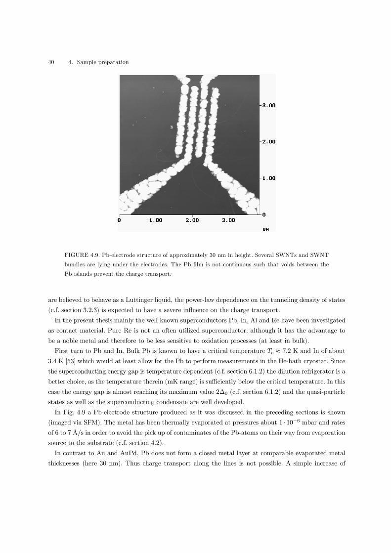
40 4. Sample preparation
FIGURE 4.9. Pb-electrode structure of approximately 30 nm in height. Several SWNTs and SWNT
bundles are lying under the electrodes. The Pb film is not continuous such that voids between the
Pb islands prevent the charge transport.
are believed to behave as a Luttinger liquid, the power-law dependence on the tunneling density of states
(c.f. section 3.2.3) is expected to have a severe influence on the charge transport.
In the present thesis mainly the well-known superconductors Pb, In, Al and Re have been investigated
as contact material. Pure Re is not an often utilized superconductor, although it has the advantage to
be a noble metal and therefore to be less sensitive to oxidation processes (at least in bulk).
First turn to Pb and In. Bulk Pb is known to have a critical temperature Tc ≈ 7.2 K and In of about3.4 K [53] which would at least allow for the Pb to perform measurements in the He-bath cryostat. Since
the superconducting energy gap is temperature dependent (c.f. section 6.1.2) the dilution refrigerator is a
better choice, as the temperature therein (mK range) is sufficiently below the critical temperature. In this
case the energy gap is almost reaching its maximum value 2∆0 (c.f. section 6.1.2) and the quasi-particle
states as well as the superconducting condensate are well developed.
In Fig. 4.9 a Pb-electrode structure produced as it was discussed in the preceding sections is shown
(imaged via SFM). The metal has been thermally evaporated at pressures about 1 · 10−6 mbar and ratesof 6 to 7 Å/s in order to avoid the pick up of contaminates of the Pb-atoms on their way from evaporation
source to the substrate (c.f. section 4.2).
In contrast to Au and AuPd, Pb does not form a closed metal layer at comparable evaporated metal
thicknesses (here 30 nm). Thus charge transport along the lines is not possible. A simple increase of

4.4 Increase of electrical coupling between metal and SWNT: room temperature measurements 41
FIGURE 4.10. Au/Pb double-structure. The thin layer (7 nm) on top of the Pb film (40 nm) seems
to fill the vacancies between the Pb-islands. However, the oxidation of these types of samples could
not be prevented by the covering Au film.
the layer thickness in order to get continuous lines is prohibited by the height of the total PMMA layer,
leading to considerable problems during the lift-off process as already discussed in section 4.2. In addition,
the thin Pb layers oxidize too fast and completely in air, such that even if the layers are continuous, a
traversing current could not be observed.
In order to overcome these problems, instead of pure Pb a double-structure Au/Pb was evaporated
with thicknesses 7 nm and 40 nm, respectively. Au was chosen as an additional material, since thin Au
films on top of Pb become superconducting due to the proximity effect [50]. Fig. 4.10 shows the inner
part of a Au/Pb-electrode structure. The voids between the Pb particles seem to be filled by Au. The
lift-off process in this type of structure is almost as clean as before. However, the starting resistance of
some MΩ of samples contacting SWNTs increased within a few minutes, such that no current could be
driven any more through the device. Thus, the oxidation of the Pb layer could only hardly be prevented
by the additional covering Au layer.
The metal In is much less oxidizing in air than Pb [54], which was the second superconducting material
investigated. Fig. 4.11 shows an SFM image of a In-electrode structure (thickness 28 nm). The In was
thermally evaporated at about 1 · 10−6 mbar at about 2 to 3 Å/s. Similar to Pb, the lift-off process isnot too dirty and the metal layer is not continuous. In comparison, the metal islands formed by In are
approximately half of the size of the Pb islands in Fig. 4.9 and tend to a more circular shape.

42 4. Sample preparation
FIGURE 4.11. SFM image of 28 nm high In-electrode structure. The structure of the In electrode
lines is comparable to the Pb case, but the island size is roughly halved. Also the lines are not
continuous as required for electrical transport.
To achieve a coherent layer, a thin silver (Ag) film (8 nm) was evaporated before the In (25 nm)
as Ag/In systems are also known to be superconducting due to the proximity effect [50]. An electrode
structure performed in this way is shown in Fig. 4.12. Apparently, the lift-off process did not deteriorate.
The In behaves different on a surface of the Ag layer than on the silanized SiO2 surface in Fig. 4.11. On
the Ag surface, the In seems to build up a continuous-like layer.
For charge transport measurements, SWNTs have been adsorbed on top of the Ag/In electrodes. The
resistance of connected SWNTs were of the order of GΩ, probably due to a thin oxidation layer on the
In [54].
In order to achieve a better electrical contact, it was tried to increase the contact area between metal
and SWNTs. For this, the samples have been annealed in a H2/N2 atmosphere at temperatures up to
125 C (Tmelting = 156.61 C for In and 961.93 C for Ag) for 1 to 2 min with the intent to submerge
the SWNTs into the In. In Fig. 4.13 scanning electron microscopy images of a structure annealed at 125C are shown.
After annealing, the In organizes in a network-like structure (Fig. 4.13b). From the inner structure
(Fig. 4.13a) the In is in great parts removed, but the Ag remained. As no additional particles between
the electrodes are observable, it seems that during annealing the In is that mobile on the Ag that it was
drawn to the outer parts of the electrodes due to the reorganizations of the In under heating. Thus no
suitable electrode structure could be developed on that basis.
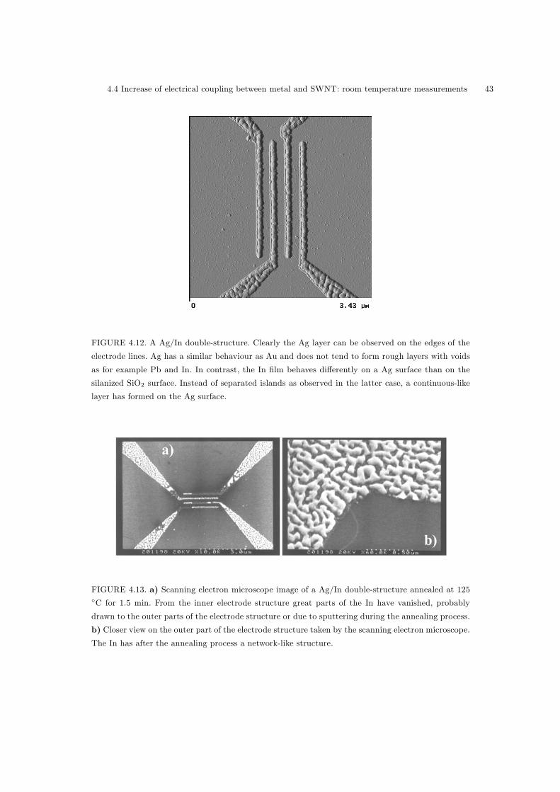
4.4 Increase of electrical coupling between metal and SWNT: room temperature measurements 43
FIGURE 4.12. A Ag/In double-structure. Clearly the Ag layer can be observed on the edges of the
electrode lines. Ag has a similar behaviour as Au and does not tend to form rough layers with voids
as for example Pb and In. In contrast, the In film behaves differently on a Ag surface than on the
silanized SiO2 surface. Instead of separated islands as observed in the latter case, a continuous-like
layer has formed on the Ag surface.
FIGURE 4.13. a) Scanning electron microscope image of a Ag/In double-structure annealed at 125C for 1.5 min. From the inner electrode structure great parts of the In have vanished, probably
drawn to the outer parts of the electrode structure or due to sputtering during the annealing process.
b) Closer view on the outer part of the electrode structure taken by the scanning electron microscope.
The In has after the annealing process a network-like structure.

44 4. Sample preparation
FIGURE 4.14. Al electrode-lines on top of several SWNTs. At the edges of the lines some residues can
be found probably due to the height of the Al layer (45 nm). The lines are smooth and continuous.
However, no current could be driven through the SWNTs.
Another candidate as a superconducting electrode material is Al with a critical temperature of about
1.2 K. Al is known to oxidize very fast, yet only forming a thin oxide layer (about 2 nm). However,
properly evaporated on a substrate, the interface of Al and substrate should remain free of oxidation.
In contrast to Pb and In, to obtain sufficiently clean layers, Al has to be evaporated at lower pressures
of the order 1 · 10−9 mbar or even less. Evaporation was done by an electron beam (Tboiling ≈ 2467C of Al). Similar to Pb the evaporation rate was chosen to be relatively high (7 to 8 Å/s) in order to
avoid undesired contamination and oxidation of the Al. Fig. 4.14 shows an SFM image of a Al-electrode
structure (45 nm in height) on top of a SWNT. The electrodes are smooth, similar to Au and AuPd.
The substrate’s surface is free of residual particles, indicating that the lift-off process works sufficiently
well. Some residue, probably due to the height of the Al layer, can be found on the edges of the electrode
lines. A disadvantage though is that the adhesion properties have been found to be worse than for Au
and AuPd, which is attributed to the silanization of the SiO2 surface. After processing, the samples have
been stored in a glove-box in Ar atmosphere. However, in none of the produced samples a current could
be driven through the contacted SWNTs at room temperature up to a few volts. It could be verified that
the electrodes are still conducting (less than 2 kΩ), even after exposure to air after several days, such
that a complete oxidation of the Al can be excluded.
As Al is very sensitive to oxidation, the observation was assumed to originate from an oxidation layer
between the SWNT and the Al which may have formed due to a residual water film on the substrate. In

4.4 Increase of electrical coupling between metal and SWNT: room temperature measurements 45
FIGURE 4.15. Sandwich-structure Au/Al/Au with a total height of about 74 nm. At the edges of the
electrode lines large residues from an imperfect lift-off process are apparent. The residues partially
short-circuit the structure.
order to remove this film, the substrate was sputtered with argon (Ar) ions in the evaporation chamber
before the evaporation of Al. But, also in these types of samples no current could be measured indicating
that if there is an oxide layer, it does not originate from residual water on the substrate. As already
mentioned, the adhesion of the Al to the surface was weaker than in the case of Au and AuPd, such that
locally and in particular in the regions where the nanotubes are lying under the Al, an oxidation film
may have formed due to a geometrical gap (c.f. section 4.4.2).
To counteract this possible problem, similar to Pb and In, a sandwich structure Au/Al/Au was trialled.
The thicknesses were 7 nm for Au and 60 nm for Al (Fig. 4.15). The thickness of the Al was increased as
within this type of structures the Al is covered on two sides by Au. Due to the proximity effect the critical
temperature of the normal metal/superconductor structure decreases with increased Au thickness. The
aim of the increased Al thickness, therefore, was to prevent the critical temperature of the structure
not to decrease significantly below the critical temperature of pure Al. The lift-off process for these
structures is not as clean as it was before, and short-circuits have been observed. This behaviour is likely
to originate from the huge height of the metal sandwich layer (approximately 74 nm) in contrast to
the PMMA layer (c.f. section 4.2). However, surprisingly, again no current could be driven through the
SWNTs in these structures, which was also observed by Buitelaar et al. for MWNTs [55] under similar
conditions. According to these results, a possible explanation may be that a pressure of 1 · 10−9 mbar is
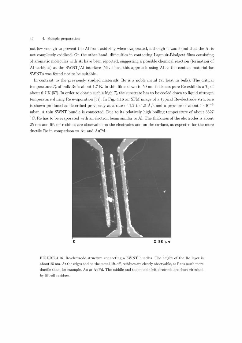
46 4. Sample preparation
not low enough to prevent the Al from oxidizing when evaporated, although it was found that the Al is
not completely oxidized. On the other hand, difficulties in contacting Lagmuir-Blodgett films consisting
of aromatic molecules with Al have been reported, suggesting a possible chemical reaction (formation of
Al carbides) at the SWNT/Al interface [56]. Thus, this approach using Al as the contact material for
SWNTs was found not to be suitable.
In contrast to the previously studied materials, Re is a noble metal (at least in bulk). The critical
temperature Tc of bulk Re is about 1.7 K. In thin films down to 50 nm thickness pure Re exhibits a Tc of
about 6.7 K [57]. In order to obtain such a high Tc the substrate has to be cooled down to liquid nitrogen
temperature during Re evaporation [57]. In Fig. 4.16 an SFM image of a typical Re-electrode structure
is shown produced as described previously at a rate of 1.2 to 1.5 Å/s and a pressure of about 1 · 10−6mbar. A thin SWNT bundle is connected. Due to its relatively high boiling temperature of about 5627C, Re has to be evaporated with an electron beam similar to Al. The thickness of the electrodes is about
25 nm and lift-off residues are observable on the electrodes and on the surface, as expected for the more
ductile Re in comparison to Au and AuPd.
FIGURE 4.16. Re-electrode structure connecting a SWNT bundles. The height of the Re layer is
about 25 nm. At the edges and on the metal lift-off, residues are clearly observable, as Re is much more
ductile than, for example, Au or AuPd. The middle and the outside left electrode are short-circuited
by lift-off residues.

4.4 Increase of electrical coupling between metal and SWNT: room temperature measurements 47
FIGURE 4.17. I/V -characteristics of the continuous line and the two in parallel connected SWNT
bundles shown in Fig. 4.16.
During the studies it was further found, that Re has a high affinity to the silanized SiO2 surface also
in the lift-off acetone bath (c.f. section 4.2). The problem of residues could be diminished by hanging the
samples freely in the middle of the vessel for the lift-off process with the Re structure pointing to the
vessel’s bottom. By this procedure, the amount of residues on the substrate’s surface could be reduced.
The observed adhesion properties are comparable to, yet better than those of Al. During the studies
it was found that the thin Re-layer is more sensitive to exposure to air than the bulk material. This was
indicated by change of colour of the thin Re layers from metallic yellow to a dim blue and the considerable
increase of the resistance of the continuous electrode lines of the Re-electrode structures (see also in the
discussion below).
Therefore, after processing, the samples have been stored in a glove-box in Ar atmosphere. However,
the oxidation process turned out to be relevant after several days only, so that the samples could be
easily handled compared to Pb or Al.
In Fig. 4.17 the I/V -characteristics in 4He atmosphere of the middle and outer-right electrode contacted
SWNT bundle in Fig. 4.16 is shown. The other pair is short-circuited due to lift-off residues. The two-
terminal resistance of the SWNT bundle was found to be about 8 MΩ, whereas the continuous line shows
a resistance of 8 kΩ. In samples exposed to air longer than several days, the resistance of the continuous
Re-line was found to increase up to orders of magnitude.
In almost all investigated Re-electrode structures, the resistance of the contacted SWNTs was be-
tween one and a few MΩs. Only a few samples (non-oxidized) were found to exhibit significantly higher
resistances (c.f. section 6.3).
In order to investigate the origin of this relatively high resistance range, Re samples have been prepared
without cooling the substrate. The reason for this is the circumstance that as the substrate is cooled
before the Re evaporation, it acts as a cold trap. Thus, residual contaminations in the evaporation
chamber may be attracted to the substrate’s surface. This in turn can influence the contact area between
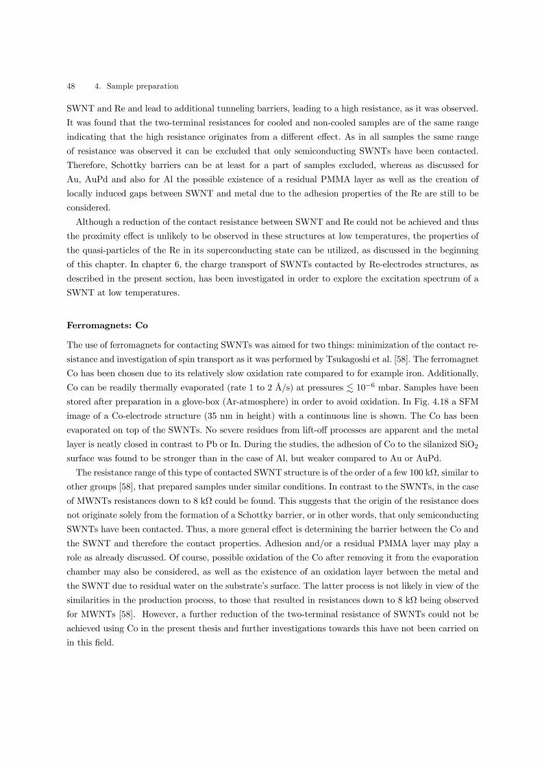
48 4. Sample preparation
SWNT and Re and lead to additional tunneling barriers, leading to a high resistance, as it was observed.
It was found that the two-terminal resistances for cooled and non-cooled samples are of the same range
indicating that the high resistance originates from a different effect. As in all samples the same range
of resistance was observed it can be excluded that only semiconducting SWNTs have been contacted.
Therefore, Schottky barriers can be at least for a part of samples excluded, whereas as discussed for
Au, AuPd and also for Al the possible existence of a residual PMMA layer as well as the creation of
locally induced gaps between SWNT and metal due to the adhesion properties of the Re are still to be
considered.
Although a reduction of the contact resistance between SWNT and Re could not be achieved and thus
the proximity effect is unlikely to be observed in these structures at low temperatures, the properties of
the quasi-particles of the Re in its superconducting state can be utilized, as discussed in the beginning
of this chapter. In chapter 6, the charge transport of SWNTs contacted by Re-electrodes structures, as
described in the present section, has been investigated in order to explore the excitation spectrum of a
SWNT at low temperatures.
Ferromagnets: Co
The use of ferromagnets for contacting SWNTs was aimed for two things: minimization of the contact re-
sistance and investigation of spin transport as it was performed by Tsukagoshi et al. [58]. The ferromagnet
Co has been chosen due to its relatively slow oxidation rate compared to for example iron. Additionally,
Co can be readily thermally evaporated (rate 1 to 2 Å/s) at pressures . 10−6 mbar. Samples have beenstored after preparation in a glove-box (Ar-atmosphere) in order to avoid oxidation. In Fig. 4.18 a SFM
image of a Co-electrode structure (35 nm in height) with a continuous line is shown. The Co has been
evaporated on top of the SWNTs. No severe residues from lift-off processes are apparent and the metal
layer is neatly closed in contrast to Pb or In. During the studies, the adhesion of Co to the silanized SiO2surface was found to be stronger than in the case of Al, but weaker compared to Au or AuPd.
The resistance range of this type of contacted SWNT structure is of the order of a few 100 kΩ, similar to
other groups [58], that prepared samples under similar conditions. In contrast to the SWNTs, in the case
of MWNTs resistances down to 8 kΩ could be found. This suggests that the origin of the resistance does
not originate solely from the formation of a Schottky barrier, or in other words, that only semiconducting
SWNTs have been contacted. Thus, a more general effect is determining the barrier between the Co and
the SWNT and therefore the contact properties. Adhesion and/or a residual PMMA layer may play a
role as already discussed. Of course, possible oxidation of the Co after removing it from the evaporation
chamber may also be considered, as well as the existence of an oxidation layer between the metal and
the SWNT due to residual water on the substrate’s surface. The latter process is not likely in view of the
similarities in the production process, to those that resulted in resistances down to 8 kΩ being observed
for MWNTs [58]. However, a further reduction of the two-terminal resistance of SWNTs could not be
achieved using Co in the present thesis and further investigations towards this have not been carried on
in this field.

4.4 Increase of electrical coupling between metal and SWNT: room temperature measurements 49
FIGURE 4.18. SFM image of a typical 35 nm thick Co-electrode structure on top of the SWNTs. The
electrode lines are continuous and smooth and only small amounts of lift-off residues are observed.
4.4.2 Alternative approaches: linker molecules and annealing
In this section, two alternative approaches are briefly described which have been tried in the framework
of this thesis, attempting to increase the electrical coupling between SWNTs and metal electrodes.
Contacting via azido molecules
This approach is based on the idea that thiol groups (-SH) have strong affinity to noble metal surfaces.
The coupling of the sulphur atom of the thiol group mediates this affinity. The electrical coupling of the
sulfur atom to the noble metal is relatively good such that charge transport is possible through this link
as it was demonstrated previously on several molecules with thiol groups [59].
In the present work, the molecule that has been chosen was 4-azidophenyl disulfide (see Fig. 4.19a)
which consists mainly of two aromatic rings (with a N3-group) which are connected via a disulfide
bridge. In contact with a noble metal the molecule dissociates into two identical parts, each of them
then chemisorbing to the metal surface via one sulfur atom (see Fig. 4.19a). The electrical connection
to the SWNT was tried to achieve via the N3-group: in ultra-violet (UV) light, a N2-molecule separates,
leaving a positively charged N-group at the aromatic ring (Fig. 4.19b). This positively charged group is
highly reactive with respect to conjugated bonding to C-C-double bonds. Thus, when a SWNT is brought
into contact with the positively charged group, locally a C-C-double bond will split and form a covalent
bonding to the SWNT as illustrated in Fig. 4.19c.
Experimentally, the described procedure has been performed on predefined electrode patterns in Ar-
atmosphere in order to avoid any undesired side products during UV-light exposure. After the chemisorp-

50 4. Sample preparation
FIGURE 4.19. Principle of connecting CNTs to noble metal surfaces via azido-molecules. a) the
molecule 4-azidophenyl disulfide dissociates at the metal surface and bonds chemically via the thiol
group (substrate: dark grey). b) After CNT adsorption, the sample is irradiated with UV light, such
that the N3-groups separate a N2 molecule. c) The remaining amino-group after N2 separation is
extremely active to C-C-double bonds and allows therefore a covalent bonding to the CNT π-system.
tion of the 4-azidophenyl disulfide from an ethylacetate solution for 24 h, SWNTs are adsorbed (15 min)
on top of the electrodes from aqueous dispersion (c.f. section 4.1). Finally the sample is exposed for 20
min to UV-light. During the studies it was found that the amount of SWNTs adsorbed in a given time
interval was considerably larger than without the chemisorption of the 4-azidophenyl disulfide. After
SWNT adsorption the sample was exposed for 2 h to UV-light. However, the two-terminal resistances
found in all samples have been in the range of a few MΩ, similar to simply adsorbed SWNTs on top of
predefined electrodes.
As the flexibility of SWNTs is rather high, most likely bending defects during the nestling against
the electrodes have formed. These lead to local gaps in the electronic structure of the SWNTs [71] and
thus to a high contact resistance (see section 6.1.1 for more details). Therefore it was not possible to
distinguish whether, the coupling to the SWNT via the N-atom was successful or not.
Annealing
The principle idea of this approach is to ”melt” SWNTs into metal electrodes as it was also shown for the
case of Ag/In electrodes. The increased contact area should lead to a reduction of the contact resistance,

4.5 Optimum choice of method for sample preparation 51
FIGURE 4.20. a) AuGe-electrode structure connecting several SWNTs before the annealing process.
The electrodes are about 20 nm in height. No severe lift-off residues are observed and the metal layer
is flat. b) After the annealing process, the structure of the AuGe electrodes has changed. Instead of
a smooth metal surface, a granular-like structure is apparent. Whether the SWNTs have melted into
the metal contact could not be determined.
that is, an increased electrical coupling. In addition the contact between metal and SWNT should be
more intimate after annealing, also supporting an increased electrical coupling.
AuGe was chosen as electrode material because in thin films AuGe melts at considerably lower tem-
peratures than in bulk (937.4 C and 1064.43 C for Au and Ge, respectively). In addition AuGe does
not sputter during the annealing process in same amounts as pure Au, which could destroy the inner
electrode structure as it was observed for the Ag/In-structures (see Fig. 4.13).
The predefined AuGe electrodes have been produced in the same way as described in section 4.2.
After adsorbtion of SWNTs on top of the electrodes, the sample was annealed in a two step process in
N2/H2-atmosphere at 300 mbar. The first step lasted for a period of 120 s at 380 C, the second at 450C for 50 s. In Fig. 4.20a and b, SFM images before and after the annealing process, respectively, of the
same electrode structure are shown. After annealing the roughness of AuGe layer increased considerably.
On the basis of the SFM-images it was not possible to resolve whether the SWNTs are ”melted” into
the electrodes. However, the two-terminal resistances of all investigated devices of this type turned out
to be in the MΩ regime. Similar to the case of the azido molecules, it remained unclear whether the high
resistance originates from tube bending or unsuccessful annealing.
4.5 Optimum choice of method for sample preparation
In this chapter various metals and methods have been presented in order to increase the electrical
coupling to the SWNTs. It was found that the contacting of SWNTs from top by AuPd and Au was best
in achieving this goal.

52 4. Sample preparation
For the requirements of the experimental investigation in the present thesis on the influence of con-
tacting electrodes on the ballistic transport (chapter 5) at room temperature and the electrical transport
in magnetic field parallel to the SWNT symmetry axis (chapter 7) at low temperatures, contacting with
AuPd is therefore most suitable.
The experiments on the superconductors revealed that the use of Re does not lead to strong electrical
coupling to the SWNT. At low temperatures therefore single-electron effects are likely. Yet, due to its
superconductor properties, Re is also well suitable: the density of states of the single-particle excitations
of the superconductor groundstate can be used as a probe for investigating the excitation spectrum of
the SWNTs (chapter 6).
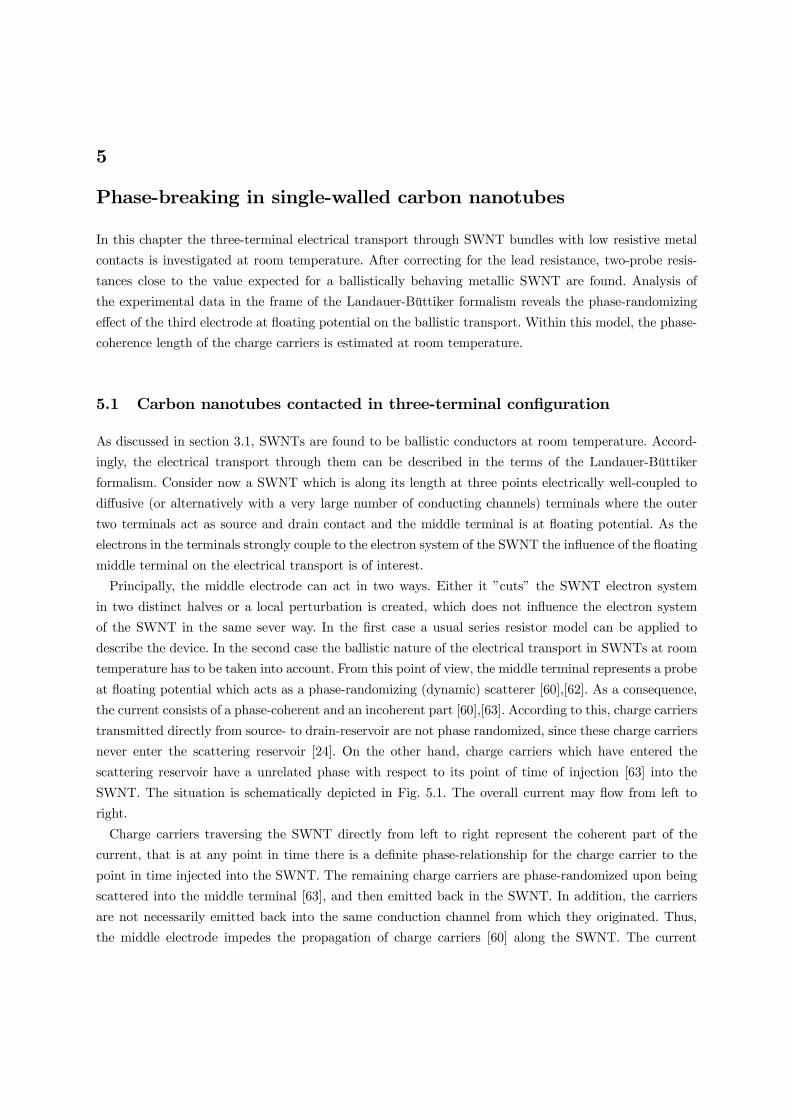
5
Phase-breaking in single-walled carbon nanotubes
In this chapter the three-terminal electrical transport through SWNT bundles with low resistive metal
contacts is investigated at room temperature. After correcting for the lead resistance, two-probe resis-
tances close to the value expected for a ballistically behaving metallic SWNT are found. Analysis of
the experimental data in the frame of the Landauer-Büttiker formalism reveals the phase-randomizing
effect of the third electrode at floating potential on the ballistic transport. Within this model, the phase-
coherence length of the charge carriers is estimated at room temperature.
5.1 Carbon nanotubes contacted in three-terminal configuration
As discussed in section 3.1, SWNTs are found to be ballistic conductors at room temperature. Accord-
ingly, the electrical transport through them can be described in the terms of the Landauer-Büttiker
formalism. Consider now a SWNT which is along its length at three points electrically well-coupled to
diffusive (or alternatively with a very large number of conducting channels) terminals where the outer
two terminals act as source and drain contact and the middle terminal is at floating potential. As the
electrons in the terminals strongly couple to the electron system of the SWNT the influence of the floating
middle terminal on the electrical transport is of interest.
Principally, the middle electrode can act in two ways. Either it ”cuts” the SWNT electron system
in two distinct halves or a local perturbation is created, which does not influence the electron system
of the SWNT in the same sever way. In the first case a usual series resistor model can be applied to
describe the device. In the second case the ballistic nature of the electrical transport in SWNTs at room
temperature has to be taken into account. From this point of view, the middle terminal represents a probe
at floating potential which acts as a phase-randomizing (dynamic) scatterer [60],[62]. As a consequence,
the current consists of a phase-coherent and an incoherent part [60],[63]. According to this, charge carriers
transmitted directly from source- to drain-reservoir are not phase randomized, since these charge carriers
never enter the scattering reservoir [24]. On the other hand, charge carriers which have entered the
scattering reservoir have a unrelated phase with respect to its point of time of injection [63] into the
SWNT. The situation is schematically depicted in Fig. 5.1. The overall current may flow from left to
right.
Charge carriers traversing the SWNT directly from left to right represent the coherent part of the
current, that is at any point in time there is a definite phase-relationship for the charge carrier to the
point in time injected into the SWNT. The remaining charge carriers are phase-randomized upon being
scattered into the middle terminal [63], and then emitted back in the SWNT. In addition, the carriers
are not necessarily emitted back into the same conduction channel from which they originated. Thus,
the middle electrode impedes the propagation of charge carriers [60] along the SWNT. The current
54 5. Phase-breaking in single-walled carbon nanotubes
FIGURE 5.1. Schematic illustration of the action of the middle electrode at floating potential (trian-
gle). The current may flow from left to right. The black lines within the SWNT and indicated for the
middle electrode represent conducting channels. The transmission coefficients directly from left to
right lead T LR and between neighbouring leads T SL and T SR are denoted by arrows. Due to the scat-
tering process, coherently passing charge (solid arrow within triangle) as well as non-coherent charge
carriers are apparent. µj (j = L,R) and µS are the electrochemical potentials of the source-drain
terminals and the floating terminal, respectively. The voltage applied is (µL - µR)/e.
through such kind of device can be derived following the line of references [61] and [60]: in Fig. 5.1
there are two channels present at the left side of the floating electrode, two channels at the right and N
channels (N >> 1) in the floating electrode itself. The current in each channel n is denoted by in and
the electrochemical potentials are given as µL, µR and µS for the left, right and the scattering charge
carrier reservoir, respectively. As the scatterer is at floating potential, the current in it is zero [24]
IS =Xn∈S
in = 0 (5.1)
and for the currents attributed to left and right lead IL and IR, respectively, it follows |IL| = |IR| .Electrons incident, say, from the left lead into the SWNT, principally have a certain probability to
be reflected at the metal/SWNT interface. As the SWNT provides two conducting channels, there exist
also a probability rL,mn that an incident electron is not reflected back into the channel m from where
it originates, but into the other channel n (m,n = 1, 2). Therefore the total probability of an electron
being reflected into the left lead is given by [61]
RL =Xm,n
RL,mn. (5.2)
Similarly, the total reflection probability for the right lead and the floating electrode is given by
RR =Pm,nRR,mn and RS =
Pm,nRS,mn, respectively. In the same way, the total probability for an

5.1 Carbon nanotubes contacted in three-terminal configuration 55
incident electron to be transmitted from lead i to lead j yields
Tij =Xm,n
Tij,mn (5.3)
where Tij,mn describes the probability of an electron in channel m in lead i to be transmitted to channel
n in lead j.
Now, let µref be some reference potential which is smaller than or equal to the lowest of the three
potentials µL, µR and µS [61]. Physically, µref indicates the electrochemical potential up to which the
same amount of positive and negative wave-vectors are present in a lead. That is, all states together
have a zero net velocity, which in turn implies a zero net current for these states in each of the leads
[61]. Thus, only the energy range δµi ≡ µi − µref , i = L,R, S, is contributing to the current and to beconsidered.
The current in each of the leads i, and thus in this part of the SWNT connected to it, consist of two
parts [60],[61]: (i) the reflected current for each of the channels (2e/h)(1 − Ri)δµi. All these currentssum up to (2e/h)(Ni−Ri)δµi, where Ni is the number of conducting channels. And (ii) the transmittedcurrent for each of the channels −(2e/h)Tijδµj (the minus sign indicates the opposite direction of thecurrents). Therefore the total current flowing in lead i is given by [61]
Ii =2e
h
(Ni −Ri)δµi −Xi6=jTijδµj
= 2e
h
(Ni −Ri)µi −Xi 6=j
Tijµj
(5.4)
where the second equality is due to the cancellation of all terms multiplied with µref .
From the boundary condition (5.1) and (5.4) it follows for the electrochemical potential of the floating
electrode
0 =2e
h
(NS −RS)µS − Xj=L,R
TSjµj
(5.5)
⇔ µS =TSLµL + TSRµR(NS −RS) =
TSLµL + TSRµRTSL + TSR
.
With the aid of (5.4), (5.5) and recalling that |IL| = |IR|, the resistance in a two-terminal configuration,where the source-drain-voltage Vsd = (µL − µR)/e is applied between left and right reservoir and themiddle electrode is at floating potential, can be calculated to
R3-terminal =Vsd|IL| (5.6)
=h
2e2(µL − µR)
·TLRTSL + TLRTSR + TSLTSR
TSL + TSR(µL − µR)
¸−1=
h
2e2TSL + TSR
TLRTSL + TLRTSR + TSLTSR
≡ h
2e2T−1eff
for which the identity NL −RL = TSL + TLR has been used.

56 5. Phase-breaking in single-walled carbon nanotubes
FIGURE 5.2. Au-electrode structure connecting two bundles ((1) and (2)) in parallel with three
electrodes. The resistances R(I), R(II) and R(III) obey the relation R(I)+R(II)≥ R(III), in contrastto normal series resistor configurations.
In the limit that the middle-electrode is ”cutting” the SWNT electronically into two pieces, i.e., all
electrons enter the middle electrode and are therefore phase-randomized, the transmission probability
TLR to get directly from left to right lead is zero and (5.6) reduces to
R3-terminal =h
2e2
µ1
TSR+
1
TSL
¶(5.7)
which is just the expression for a usual series resistor model. Assuming now that the transmission from
one lead to the neighbouring are perfect, one finds TSR = TSL = 2, as a metallic ballistically conducting
SWNT has two conducting channels, and thus R3-terminal = h/2e2 ≈ 12.9 kΩ and Teff = 1. Otherwise,if the middle electrode at floating potential is not dividing the SWNT into two electrically distinct parts,
R3-terminal < h/2e2 and Teff > 1.
5.2 Experimental data and discussion
SWNTs were contacted with electrodes on top as described in section 4.2 and as electrode material Au
and AuPd has been used. An SFM image of a Au-electrode structure (20 nm in height) is shown in Fig.
5.2. The electrodes are about 100 nm apart from each other and approximately 100 nm in width.
Two SWNT bundles (1) and (2) are contacted in parallel to the same three electrode lines. The height
of the bundles is about 3 nm and 5 nm for bundle (1) and (2), respectively. The two-terminal resistances

5.2 Experimental data and discussion 57
FIGURE 5.3. SFM image of three AuPd electrode lines contacting a thin SWNT bundle (height ≈3 nm). Inset: cross-sectional analysis along the outright electrode stripe. The profile of the bundle
clearly presses through the electrodes, revealing a height of about 3 nm (see triangles).
measured at room temperature in vacuum for the three possible combination of electrodes as source
and drain (see Fig. 5.2) are R(I) = (6.5± 0.2) kΩ, R(II) = (6.1± 0.2) kΩ and R(III) = (10.3± 0.3)kΩ, where in the last case the middle electrode Φ was floating. The resistances R(I) and R(II) are
low such that a good electrical coupling between each metal electrode and SWNT can be assumed.
However, R(III) < R(I) + R(II) is not in agreement with normal conductors/resistors in series where
R(III) ≥ R(I) + R(II) is expected. In view of the discussion in section 5.1, if the SWNTs investigatedhere are ballistic then the relation R(III) < R(I) +R(II) points towards the phase-randomizing effect of
a probe attached.
In order to explore the influence of the floating middle electrode in more detail, instead of four separate
electrode fingers, electrode arrays consisting of three equidistant stripes were prepared using AuPd (see
Fig. 5.3) as electrode material for the better lift-off process. A continuous electrode line which can be
electrically connected at both ends has also been generated and allows to seek for corrections due to the
lead resistance.
An SFM image of a typical sample investigated is shown in Fig. 5.3. A thin SWNT bundle is connected
to three AuPd electrodes (about 17 nm in height). The electrode stripes are separated by 100 nm, and
are approximately 100 nm in width. The electrical transport measurements were performed under the
same conditions as the previously described measurements. In the upper inset of Fig. 5.3, the SFM
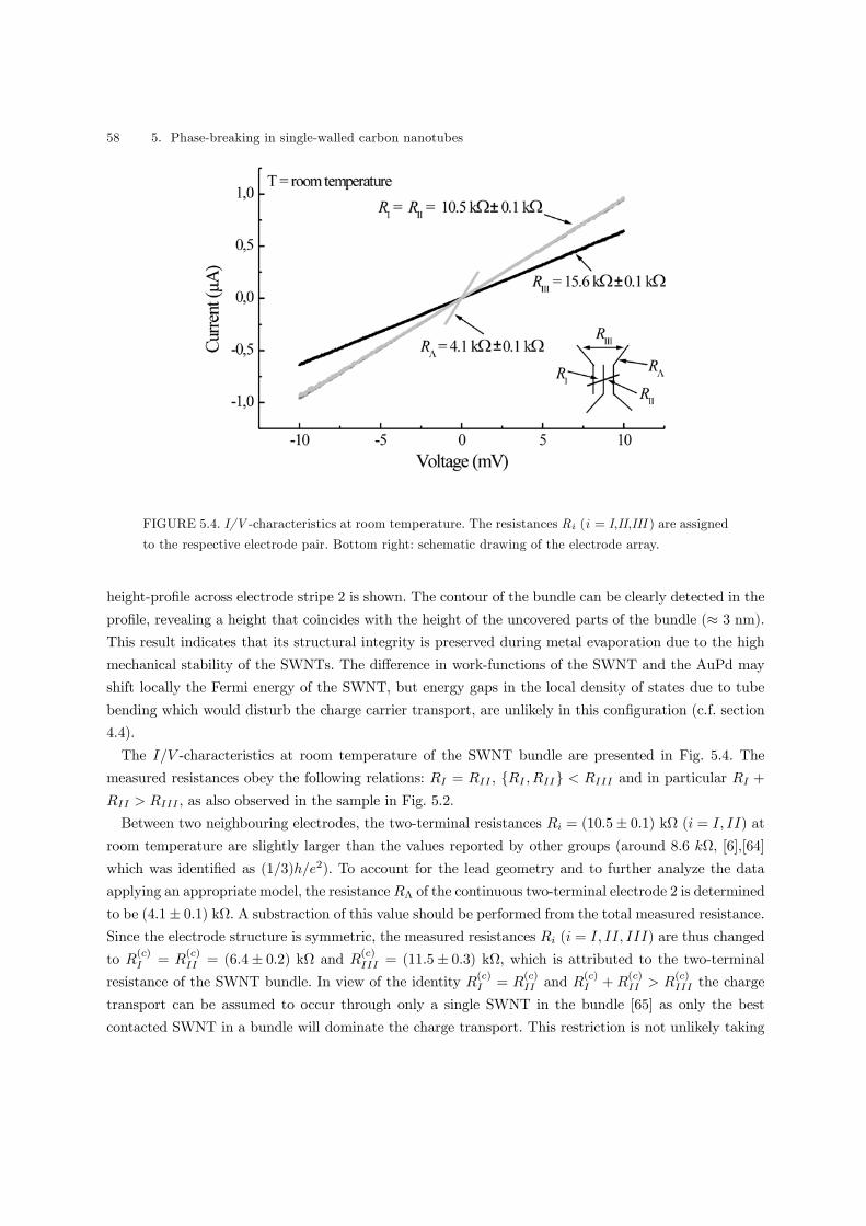
58 5. Phase-breaking in single-walled carbon nanotubes
FIGURE 5.4. I/V -characteristics at room temperature. The resistances Ri (i = I,II,III ) are assigned
to the respective electrode pair. Bottom right: schematic drawing of the electrode array.
height-profile across electrode stripe 2 is shown. The contour of the bundle can be clearly detected in the
profile, revealing a height that coincides with the height of the uncovered parts of the bundle (≈ 3 nm).This result indicates that its structural integrity is preserved during metal evaporation due to the high
mechanical stability of the SWNTs. The difference in work-functions of the SWNT and the AuPd may
shift locally the Fermi energy of the SWNT, but energy gaps in the local density of states due to tube
bending which would disturb the charge carrier transport, are unlikely in this configuration (c.f. section
4.4).
The I/V -characteristics at room temperature of the SWNT bundle are presented in Fig. 5.4. The
measured resistances obey the following relations: RI = RII , RI ,RII < RIII and in particular RI +RII > RIII , as also observed in the sample in Fig. 5.2.
Between two neighbouring electrodes, the two-terminal resistances Ri = (10.5± 0.1) kΩ (i = I, II) atroom temperature are slightly larger than the values reported by other groups (around 8.6 kΩ, [6],[64]
which was identified as (1/3)h/e2). To account for the lead geometry and to further analyze the data
applying an appropriate model, the resistanceRΛ of the continuous two-terminal electrode 2 is determined
to be (4.1± 0.1) kΩ. A substraction of this value should be performed from the total measured resistance.Since the electrode structure is symmetric, the measured resistances Ri (i = I, II, III) are thus changed
to R(c)I = R(c)II = (6.4± 0.2) kΩ and R(c)III = (11.5± 0.3) kΩ, which is attributed to the two-terminal
resistance of the SWNT bundle. In view of the identity R(c)I = R(c)II and R
(c)I + R
(c)II > R
(c)III the charge
transport can be assumed to occur through only a single SWNT in the bundle [65] as only the best
contacted SWNT in a bundle will dominate the charge transport. This restriction is not unlikely taking

5.2 Experimental data and discussion 59
FIGURE 5.5. a) Room-temperature resistance of the SWNT in Fig. 5.2 in the configuration measured
as depicted in the lower right inset. b) The equivalent circuit of this configuration.
into account the very sensitive nature of the contacting process as illustrated in the discussions in section
4.2 an 4.4.
In order to support the conclusions drawn above, electrical transport on the same device is measured
in a different contacting configuration. The equivalent circuit of this configuration is depicted in Fig.
5.5b. In this configuration, the middle electrode is set at varying potential and the current to the outer
two electrodes is measured. The lead resistances are estimated roughly to be R1 ≈ 2 kΩ, R2 ≈R3 ≈ 3kΩ. According to this, and assuming a resistance of 6.45 kΩ for each SWNT segment between two
neighbouring electrodes, the total resistance of the equivalent circuit is about 6.73 kΩ. This is in good
agreement with the experimental value of (7.0± 0.2) kΩ (Fig. 5.5a), recalling that only rough values forthe lead resistances R1, R2 and R3 in this configuration could be taken. Therefore, the correction for
the lead resistance as done above is a reliable analysis, and supports the corrected values R(c)I , R(c)II and
R(c)III of the measured resistances.
As for SWNTs the maximum number of spin-degenerated conducting channels is two, the traversing
current is given by
I =2e
h
Xi=1,2
Ti (µ1 − µ2) (5.6)
where µj = eVj is the electrochemical potential of electrode j (j = 1, 2). Thus the two-terminal resistance
in the case of perfect transmission, that is T1 = T2 = 1, yields
R(SWNT )2T =
h
2e2
Xi=1,2
Ti
−1 = h
4e2≈ 6.45kΩ. (5.7)
This theoretical value is in very good agreement with the corrected values of R(c)I and R(c)II , both
found to be (6.4± 0.2) kΩ in the here presented measurements, indicating that a metallic SWNT with

60 5. Phase-breaking in single-walled carbon nanotubes
two conducting channels is contacted. At this point it has to be noted, that possible reflective potential
barriers for the conducting channels at the SWNT/AuPd interface, which might originate from the
difference in the respective work-functions, are unlikely. Otherwise higher values than (6.4± 0.2) kΩ forR(c)I and R(c)II should be observed in the here presented experiments.
In addition, the conductance quantization of SWNTs is implicitly indicated by the data presented
as R(c)I and R(c)II coincide nicely with the theoretical value of R(SWNT )2T ≈ 6.45 kΩ. The conductance
quantization has up to now only been shown for the case of MWNTs [28], but neither directly nor
indirectly for SWNTs.
The identification of the investigated SWNT as being metallic and ballistically conducting, together
with the observation of the relation R(c)III < R(c)I + R
(c)II = (12.8 ± 0.2) kΩ (c.f. section 5.1), is a strong
indicator for a phase-breaking process on the charge carriers in the SWNT, which is due to the mid-
dle electrode at floating potential [63]. Therefore (5.6) for the three-terminal resistance R3-terminal is
applicable. Thus, R(c)III = R3-terminal = (h/2e2)T−1eff and leads to the effective transmission coefficient
Teff ≈ 1.2 > 1 in agreement with the discussion in section 5.1.On the basis of the experimental observations the phase-coherence length l(exp )φ for the contacted SWNT
can now be estimated. The phase-coherence length is a measure for the length, at which a definite phase-
relationship of a charge carrier is preserved (see Appendix A). As the geometrical distance between the
two outer electrodes contacting the SWNT are 300 nm, l(exp)φ can be estimated to be at least of the
same order. This magnitude coincides with other experimental works, as reported at low temperatures
for MWNTs (at T ≈ 3 K) [66] and SWNT rings (at T ≈ 3 K) [67].The phase-coherence length l(exp )φ estimated from the experimental data of about 300 nm is only a
lower border of the actual phase-coherence length l(SWNT )φ of the SWNT investigated. This can be seen
as follows: in Ref. [34] the mean free time at room-temperature for electron-phonon scattering τe−phin SWNTs was found to be approximately 18 ps. This time period corresponds to a mean free path
le−phm ≈ 14 µm for an electron before it is scattered by a phonon. As phonons are dynamic (inelastic)
scatterers [24], it immediately follows that this process limits the phase-coherence length l(SWNT )φ to be
not more than le−phm .
Beside the electron-phonon scattering, electron-electron scattering is also a dynamic process which
destroys the phase-relationship between the current carrying electrons [63]. If for the mean free time
for electron-electron scattering τe−e at room-temperature in SWNTs τe−e & τe−ph is valid, then the
phase-coherence length l(SWNT )φ is again determined by le−phm as le−em & le−phm where le−em is the mean fee
path of an electron before it is scattered by another electron.
In case τe−e < τe−ph, it follows le−em < le−phm and le−em can be determined by le−em = υF τe−e. From
the here presented experiments, the phase-coherence length l(exp )φ was found to be about 300 nm. As 300
nm << le−phm ≈ 14 µm, only the magnitude of le−em can be the limiting value for l(SWNT )φ . Therefore
setting le−em ≈ l(exp )φ , from l(exp)φ ≈ le−em = υF τe−e the mean free time τe−e can be determined to be
approximately 3.75 ms, where for the Fermi velocity υF ≈ 8 · 10−5 m/s [34] has been used. That is,τe−e >> τe−ph, which is in contradiction to the starting assumption τe−e < τe−ph. In consequence le−em

5.3 Concluding remarks 61
is of similar magnitude as le−phm and therefore l(SWNT )φ has to be of the same order of magnitude as le−em
and le−phm . That is, l(SWNT )φ >> l
(exp )φ .
Finally it is noteworthy to recall that scattering due to structural defects in the C-atom lattice of a
CNT does not affect the phase-relationship between the conducting electrons, as these types of scatterer
are static (elastic) and therefore do not have an influence on l(SWNT )φ .
5.3 Concluding remarks
In conclusion the experimental investigations presented here implicitly indicated the conductance quan-
tization for SWNTs. Further from the experimental data it could be deduced that in SWNTs at room
temperature the mean free path for electron-electron scattering le−em is comparable to the mean free
path for electron-phonon scattering le−phm ≈ 14 µm [34]. In consequence, the magnitude of le−em implies
a relatively weak electron-electron interaction in this temperature regime. From the magnitudes of le−em
and le−phm the phase-coherence length l(SWNT )φ at room temperature could be deduced to be of the same
order of magnitude.

62 5. Phase-breaking in single-walled carbon nanotubes

6
Single-electron charging and quantum wires: suppression ofquasi-particle tunneling
Single-electron charging was one of the first effects observed and investigated in electrical transport in
SWNTs [3],[4]. It could be demonstrated that SWNTs weakly connected to metal electrodes can be
used as molecular transistors [4] and the transport spectroscopies on SWNTs gave a first insight in the
electronic excitation spectrum. The experimental data have been interpreted in the framework of the
constant interaction model [68]. In particular, visible excitations were attributed to quantization effects
due to the finite length of the SWNTs under investigation. However, for most of these results of transport
spectroscopy, it has been apparent that the excitation spectrum of the SWNTs is much more complex
than predicted by the constant interaction model. It was assumed that the deviations originate from the
strong 1D character of the SWNTs but later on neither theoretical nor experimental investigations on
this type of devices in this direction have been reported. The stated assumption is only supported by the
observation of LL-like signatures in the current/voltage-characteristics of electrically strongly contacted
SWNTs towards low temperatures.
In order to seek for more evidences of the LL-like state in SWNTs, in the present chapter SWNTs
electrically weakly connected to superconducting leads are investigated at temperatures in the mK-
regime.
Due to the singular behaviour of the superconductor (SC) quasi-particle’s density of states and the LL-
like nature of SWNTs, differences in the current/voltage-characteristics are likely compared to tunneling
from Fermi-liquid (FL) -like leads into the SWNT. From the data conclusions on the excitation spectrum
of the SWNT should be allowed.
Before showing the experimental data, the general concept of a single-electron charging of an island
is introduced. The corresponding electrical transport regions for different contacting materials (FL-like
and superconducting) and islands, FL- or LL-like, are derived and then combined to the arrangement
SC/LL(SWNT)/SC. Then the experimental data is presented and qualitatively compared with the pre-
vious theoretical considerations.
6.1 Energetical situation and electrical transport regions: normal metaland superconductor leads
In this section the effects of single-electron charging on the electrical transport is presented. For this the
general energetical situation and the electrical transport regions are discussed for the case of FL-like and
SC reservoirs connected to a metallic (FL-like) island.

64 6. Single-electron charging and quantum wires: suppression of quasi-particle tunneling
6.1.1 Normal metal reservoirs
Consider an FL-like or metallic island which can be both inorganic or organic, at a potential V0 surrounded
by a number of electrodes (El: l = 1, ...,m), each at a potential Vl (see Fig. 6.1a). Further let the electrodes
be capacitively (electrically weakly) coupled to the island. In this case the tunneling barriers between the
island and each of the electrodes are that high that an electron is confined long enough onto the island
such that between tunnel events the electron is considered as being completely localized on the island1.
Therefore, the number of charges on an island in such an arrangement is quantized and the phenomenon
of single-electron charging is observable in electrical transport through the device.
If now an electron −e is added to the island, image charges δe(i) are influenced on the surroundingelectrodes, such that
Pi δe
(i) = +e. Therefore a charge polarization between the island and the electrodes
has occurred. In order to enable the polarization to form, that is, to charge the island, energy from outside
the system has to be provided. This energy is also called the charging energy of the island. Apparently,
the charging energy represents an energy barrier for the addition of an electron on the island. However,
by changing the potentials of the surrounding electrodes the charging energy can be lowered. Of course,
the same amount of energy (if Vg = 0) is necessary in order to remove an electron from the island.
In order to describe the situation from an energetical point of view, let E(n, 0; Vl) denote the ground-state energy of the n-electron system on the island for the respective potentials Vl ≡ V1, ..., Vm. In arealistic experimentm = 3, that is, Vl ≡ Vg, Vs, Vd where Vg is the potential of the gate-electrode andVs(d) the potential of the source (drain) electrode. Then the energy difference between two groundstates
energies of the n- and the n+ 1-electron system on the island can be defined as [69]
µ(n+ 1; Vl) ≡ E(n+ 1, 0; Vl)−E(n, 0; Vl). (6.1)
An excited state on the island with n electrons is denoted by the index i > 0 and has the energy
E(n, i; Vl). The index i stands for a whole set of quantum numbers characterizing the state uniquely
(i = 0 denotes for the groundstate). Transitions to excited states of systems with different number of
electrons require therefore the energy E(n+1, j; Vl)−E(n, i; Vl) , i, j ≥ 0 (i = 0, j = 0 for transitionsbetween groundstates).
The energetical situation of an island connected capacitively to two FL-like reservoirs and a gate
electrode in thermal equilibrium is depicted in Fig. 6.1b. In the situation depicted the charging energy
does not allow a current to flow through the island, and the number of electrons on the island is stable.
This effect is sometimes also termed Coulomb-Blockade. In order to enable a single electron to tunnel on
the island, the energy barrier, that is the charging energy has to be overcome by applying a finite source-
drain voltage Vsd ≡ Vs − Vd. Now, applying a finite source-drain voltage is achieved by changing thepotentials of source- and drain-electrodes. As these electrodes are capacitively coupled to the island, the
action on the island by changing these potentials is described by the corresponding capacitive couplings
1Expressed in terms of resistance, the contact resistance between the island and each of the electrodes has to be (at
least) larger than the quantum resistance RK = h/e2 ≈ 25.8 kΩ.
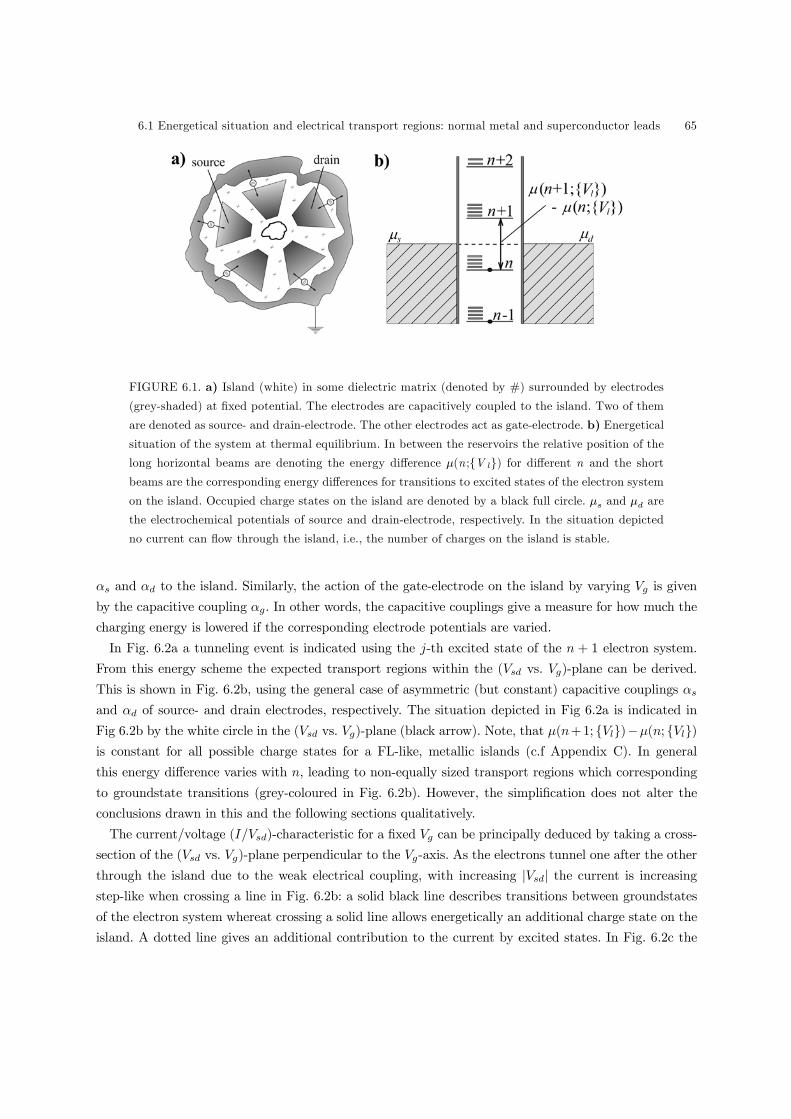
6.1 Energetical situation and electrical transport regions: normal metal and superconductor leads 65
FIGURE 6.1. a) Island (white) in some dielectric matrix (denoted by #) surrounded by electrodes
(grey-shaded) at fixed potential. The electrodes are capacitively coupled to the island. Two of them
are denoted as source- and drain-electrode. The other electrodes act as gate-electrode. b) Energetical
situation of the system at thermal equilibrium. In between the reservoirs the relative position of the
long horizontal beams are denoting the energy difference µ(n ;V l) for different n and the short
beams are the corresponding energy differences for transitions to excited states of the electron system
on the island. Occupied charge states on the island are denoted by a black full circle. µs and µd are
the electrochemical potentials of source and drain-electrode, respectively. In the situation depicted
no current can flow through the island, i.e., the number of charges on the island is stable.
αs and αd to the island. Similarly, the action of the gate-electrode on the island by varying Vg is given
by the capacitive coupling αg. In other words, the capacitive couplings give a measure for how much the
charging energy is lowered if the corresponding electrode potentials are varied.
In Fig. 6.2a a tunneling event is indicated using the j-th excited state of the n + 1 electron system.
From this energy scheme the expected transport regions within the (Vsd vs. Vg)-plane can be derived.
This is shown in Fig. 6.2b, using the general case of asymmetric (but constant) capacitive couplings αsand αd of source- and drain electrodes, respectively. The situation depicted in Fig 6.2a is indicated in
Fig 6.2b by the white circle in the (Vsd vs. Vg)-plane (black arrow). Note, that µ(n+1; Vl)−µ(n; Vl)is constant for all possible charge states for a FL-like, metallic islands (c.f Appendix C). In general
this energy difference varies with n, leading to non-equally sized transport regions which corresponding
to groundstate transitions (grey-coloured in Fig. 6.2b). However, the simplification does not alter the
conclusions drawn in this and the following sections qualitatively.
The current/voltage (I/Vsd)-characteristic for a fixed Vg can be principally deduced by taking a cross-
section of the (Vsd vs. Vg)-plane perpendicular to the Vg-axis. As the electrons tunnel one after the other
through the island due to the weak electrical coupling, with increasing |Vsd| the current is increasingstep-like when crossing a line in Fig. 6.2b: a solid black line describes transitions between groundstates
of the electron system whereat crossing a solid line allows energetically an additional charge state on the
island. A dotted line gives an additional contribution to the current by excited states. In Fig. 6.2c the
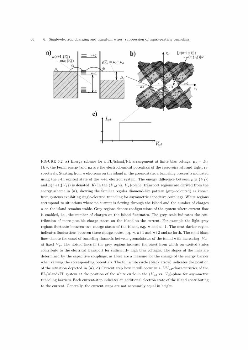
66 6. Single-electron charging and quantum wires: suppression of quasi-particle tunneling
FIGURE 6.2. a) Energy scheme for a FL/island/FL arrangement at finite bias voltage. µs = EF
(EF , the Fermi energy)and µd are the electrochemical potentials of the reservoirs left and right, re-
spectively. Starting from n electrons on the island in the groundstate, a tunneling process is indicated
using the j -th excited state of the n+1 electron system. The energy difference between µ(n ;V l)
and µ(n+1;V l) is denoted. b) In the (V sd vs. V g )-plane, transport regions are derived from the
energy scheme in (a), showing the familiar regular diamond-like pattern (grey-coloured) as known
from systems exhibiting single-electron tunneling for asymmetric capacitive couplings. White regions
correspond to situations where no current is flowing through the island and the number of charges
n on the island remains stable. Grey regions denote configurations of the system where current flow
is enabled, i.e., the number of charges on the island fluctuates. The grey scale indicates the con-
tribution of more possible charge states on the island to the current. For example the light grey
regions fluctuate between two charge states of the island, e.g. n and n+1. The next darker region
indicates fluctuations between three charge states, e.g. n, n+1 and n+2 and so forth. The solid black
lines denote the onset of tunneling channels between groundstates of the island with increasing |Vsd |at fixed V g . The dotted lines in the grey regions indicate the onset from which on excited states
contribute to the electrical transport for sufficiently high bias voltages. The slopes of the lines are
determined by the capacitive couplings, as these are a measure for the change of the energy barrier
when varying the corresponding potentials. The full white circle (black arrow) indicates the position
of the situation depicted in (a). c) Current step how it will occur in a I/V sd -characteristics of the
FL/island/FL system at the position of the white circle in the (V sd vs. V g )-plane for asymmetric
tunneling barriers. Each current-step indicates an additional electron state of the island contributing
to the current. Generally, the current steps are not necessarily equal in height.

6.1 Energetical situation and electrical transport regions: normal metal and superconductor leads 67
FIGURE 6.3. I/V sd -characteristics of a SWNT bundle deposited over platinum electrode lines mea-
sured at 4.2 K from Ref. [4]. Three curves are shown with a clear step-formation indicating that
charge transport is dominated by single-electron tunneling. The curves differ from each other as
they are measured at different backgate-voltages (A: 88.2 mV, B: 104.1 mV, C: 120 mV). Inset:
I/V sd -characteristics with a broader range of backgate-voltages. A diamond-like structure around
zero source-drain voltage is apparent, typical for the Coulomb-Blockade effect. The additional steps
are due to tunneling utilizing excited states of some groundstate.
current-step in a typical I/Vsd-characteristic for the situation in Fig. 6.2a is depicted. The height of the
current step is determined by the transition rate (see section 6.2 for more details on transition rates)
for this tunnel event, which usually varies in magnitude. Note, that the effect of single-electron charging
is observable at temperatures for which the thermal broadening of energy states of the island is smaller
than the energy difference µ(n+ 1; Vl)− µ(n; Vl)/2.Step-like features in the I/Vsd-characteristics exemplarily depicted in Fig. 6.2c were also observed in
electrical transport measurements on SWNTs adsorbed on top of predefined electrodes (Au, platinum or
AuPd) [3],[4],[70]. Two terminal room-temperature resistances for such arrangements are found to be in
the MΩ regime under ambient atmosphere. The origin of such high resistances are bending defects [71]
and native hydrocarbon adsorbate layers on the metal electrodes [72]. In consequence, before a CNT is
deposited on top of a predefined electrode structure, the electrodes are already covered by a thin (≈ 0.5nm) hydrocarbon layer which represents an additional tunneling barrier between the CNT and electrode.
In Fig. 6.3 a typical electrical transport measurement on a thin SWNT bundle in the above described
configuration at temperature T = 4.2 K at different Vg is shown [4]. Apparently, clear steps are observable
indicating that the transport along the tube is dominated by single-electron charging. The shape of the
curves change as the gate voltage is varied leading to a rhomb-like structure in the (Vsd vs. Vg)-plane
(inset Fig. 6.3). The experimental data have been interpreted in the constant interacting model (CIM)

68 6. Single-electron charging and quantum wires: suppression of quasi-particle tunneling
[68] where the steps outside the Coulomb-Blockade region (diamond-like structure in the middle of
the inset) were attributed to the existence of a discrete energy spectrum in the SWNTs. The CIM
assumes that the interactions between the electrons in the island are constant. This in turn leads to
µ(n + 1; Vl) − µ(n; Vl) = e2/C where C is a constant capacitance (see Appendix C). However,
for most results on this type of electrical transport measurements, deviations from the CIM have been
apparent. In particular, the excitation spectrum of the SWNTs is observed to be much more complex
than predicted by the CIM.
6.1.2 Superconducting reservoirs
With respect to CNTs, in literature only investigations on SWNTs electrically strongly coupled to super-
conductor leads have been reported. In these experiments indeed the proximity-effect could be observed
[51],[52], however, no additional indicators for the LL-like nature of the SWNTs nor information on their
excitation spectrum could be drawn from the data.
In the limit of weak electrical coupling of SC leads to CNTs, the tunneling barriers are that high, that
no Andreev reflection or proximity effect can occur, but only quasi-particle (QP)-tunneling. QPs are the
single-particle excitations of the superconducting groundstate and behave generally like electrons [73].
This contacting arrangement allows to utilize the properties of the QP density of states DQP (ε) as will
be shown in this and section 6.2 in combination with a LL and thus serves as a tool for probing the
excitation spectrum of a SWNT.
In case of BCS-like [73] SC instead of FL-like reservoirs for source- and drain-electrode, the energetical
situation described in section 6.1.1 changes due to the special properties of the SC. Contrary to FL-like
reservoirs DQP (ε) cannot be regarded as constant at low temperatures. Instead it is of the form [73]
DQP (ε) ∝ |ε|pε2 −∆2(T ) for |ε| > ∆(T ) (6.1)
and zero for |ε| ≤ ∆(T ). The QP energy ε is measured relatively to the electrochemical potential of the SCreservoirs and can be positive or negative. In Fig. 6.4a the DQP (ε) as a function of ε is shown: occupied
(shaded) QP energy levels are separated from the unoccupied ones by the temperature-dependent SC
energy gap 2∆(T ).
In Fig. 6.4b the energetic situation of the system for a finite source-drain voltage Vsd = (µs − µd)/eapplied at some fixed gate-voltage Vg is depicted. Without loss of generality, in this figure 2∆(T ) is chosen
to be smaller than the energy level distance µ(n+ 1; Vl) − µ(n; Vl). A tunneling event is indicatedutilizing the j-th excited state of the n+ 1 electron system.
The influence of the SC gap on the electrical transport regions is shown in Fig. 6.4c. In contrast to
islands which are connected to FL-like electrodes, for |Vsd| < 2∆(T )/e no current can flow for any valueof Vg. Along the Vg-axis a ”currentless band” of width 4∆(T )/e is formed. For comparison, additional
rhombs (dotted line) in the white regions of the (Vsd vs. Vg)-plane are shown, which corresponds to the
case of FL-like reservoirs connected to the island as described in section 6.1.1.

6.1 Energetical situation and electrical transport regions: normal metal and superconductor leads 69
FIGURE 6.4. a) QP density of states DQP(ε) as a function of QP energy ε. Occupied QP states
(grey-shaded) are separated from unoccupied states by the SC energy gap 2∆(T ). Towards the edge
of the SC energy gap the DQP(ε) shows a singular behaviour. b) Energetical situation for a QP tunnel
event through an excited state of the n+1groundstate of a metallic (FL-like) island. The transition
rates (more details in section 6.2) for the tunneling process are indicated by the black curved arrows.
c) (V sd vs. V g )-plane for the SC/metallic island (FL)/SC arrangement. The full white circle is the
position at which the energetical situation depicted in (a) is located (grey arrow). In contrast to
FL/metallic island/FL arrangements, a ”currentless band” of width 4∆(T ) has formed along the
V g -axis. For comparison the diamonds for which the number of electrons on the island is stable in
the FL/metallic island/FL arrangement (c.f. Fig. 6.2b) are denoted by the dotted (black) lines.
The I/Vsd-characteristic for a fixed Vg can again be extracted from the (Vsd vs. Vg)-plane by taking
a cross-section perpendicular to the Vg-axis. A step-like increase of the current with increasing |Vsd| isexpected as in the case of FL-like reservoirs, where the height of the steps is again determined by the
corresponding transition rates (c.f. section 6.1.2).
In Fig. 6.5a experimentally observed I/Vsd-characteristics for an inorganic, metallic island connected
to superconducting Al leads are shown [74]. Well-developed steps in the current with increasing |Vsd|are visible. However, in contrast to FL/island/FL arrangements at the onset of each current step a
pronounced peak is observed. The peaks originate from the singular behaviour of DQP (ε) for energies ε
close to the SC energy gap (see Fig. 6.4a). In Fig 6.5b an enlarged view of one of the current peaks is
plotted.

70 6. Single-electron charging and quantum wires: suppression of quasi-particle tunneling
FIGURE 6.5. a) I/V sd -characteristics of a metallic spherical island connected to superconducting Al
leads from Ref. [74]. When the Al is not superconducting due to an externally applied magnetic field,
the normal shape of the current steps as shown in section 6.1.1 is recovered. In the superconducting
state, clear peaks at the onset of each current step are observable. b) Closer view of one of a current
step for normal and superconducting electrodes. The continuous line is a theoretical fit taking the
QP density of states into account. Note that the current step in the superconducting state is shifted
relative to the same step in the normal state due to the formation of the currentless band.
In total a SC/island/SC differs from a FL/island/FL arrangement in two points: (i) development of a
currentless band along the Vg-axis in the (Vsd vs. Vg)-plane and (ii) QP tunneling induced peaks at the
onset of each current-step in the I/Vsd-characteristic, directly reflecting the DQP (ε).
6.2 Electrical transport involving the Tomonaga-Luttinger liquid
In section 6.1 the general concept of single-electron charging was discussed for FL-like and superconductor
reservoirs. In both cases a FL-like island as for example a spherical metallic particle was assumed.
However, SWNTs are by no means comparable to such an island as they exhibit a strong 1D-character
and also showed LL-like signatures in electrical transport in case of electrically strongly coupled FL-like
leads. Thus in the following instead of a FL-like island a LL-like island is discussed in view of single-
electron tunneling dominating the electrical transport.
Towards this, first the general transition rates for a tunneling process are determined from which then
the stationary current through the device can be derived. The transition rates depend on the following
physical quantities: (i) changes of the total energy for rearranging electrons in the system as a tunnel
event occurs under energy conservation, (ii) the matrix element¯t(r)i→j(ε)
¯for the tunneling of a single
electron or QP onto the island with energy ε and (iii) the number of electrons or QPs at a given energy
ε which is given by the product of the electron/QP density of states De/QP (ε) in the reservoirs and the
Fermi distribution f(ε, µr) (µr electrochemical potential of reservoir r).

6.2 Electrical transport involving the Tomonaga-Luttinger liquid 71
The transition rate for tunneling from the reservoir r onto the LL-like island inducing a transition
from the island state [n, i] to [n+ 1, j] is therefore [75],[76]
Γ(r)[n,i]→[n+1,j],e/QP =
2π
~
Z ∞−∞
¯t(r)i→j(ε)
¯2·De/QP (ε) · f(ε, µr) (6.2)
×δ(E(n+ 1, j; Vl)−E(n, i; Vl)− (µr + ε)) dε
where the delta distribution δ(E(n+ 1, j; Vl)− E(n, i; Vl)− (µr + ε)) accounts for the energy con-
servation of the tunneling process. The stationary current through the island is directly proportional to
Γ(r)[n,i]→[n+1,j],e/QP [75],[76],
I(e/QP )stat = e
Xn
Xi
Xj
nΓ(1)[n,i]→[n+1,j],e/QP − Γ(2)[n,i]→[n+1,j],e/QP
o· P[n,i] (6.3)
where the sums are over all charge states n of the island and over all excited states i and j of the n and
the n+ 1 electron system on the island, respectively. P[n,i] is the probability of finding the island in the
i-th excited n-electron state for given Vl. The latter is constrained by the conditionPn
Pi P[n,i] = 1,
but this is not vital for the following discussion. (6.3) can be simplified assuming that the system is
before each tunneling event in the groundstate of the respective electron number: the sum over i can be
cancelled except for i = 0, and for a dense excitation spectrum it is more convenient to convert the sum
over j into an integral form. For this the density of states τn+1(²) of the excitations of the n+ 1 state
has to be introduced transforming (6.2) to
Γ(r)[n,0]→[n+1,²],e/QP = [τn+1(²) d²] (6.4)
×2π~
Z ∞−∞
¯t(r)(ε)
¯2·De/QP (ε) · f(ε, µr)
×δ(µ(n+ 1; Vl) + ²− (µr + ε)) dε
where the definition E(n+ 1, ²; Vl) ≡ E(n+ 1, 0; Vl) + ² has been used and τn+1(²) d² describes the
degeneracy of the n+1-electron state at the excitation ². Carrying out the integral in (6.4) with the aid
of the delta distribution the transition rate is found to depend on the product τn+1(²) · De/QP (µ(n +1; Vl) + ²).In the case of a metallic island at low temperatures, τn+1(²) varies only slightly such that it can
be assumed to be constant. If FL-like leads are assumed then also De(ε) ≈ const which resembles thesituation described in section 6.1.1. For SC reservoirs De(ε) is replaced by DQP (ε) and the dependence of
DQP (ε) on ε mainly determines the transition rate and thus I(QP )stat . As DQP (ε) ∝ |ε| /pε2 −∆2(T ) for
|ε| > ∆(T ), I(QP )stat is strongly enhanced for QP energies |ε| close to ∆(T ). In contrast, for |ε| >> ∆(T ),I(QP )stat is smaller which in total leads to the formation of peaks at the onset of each step in the I/Vsd-
characteristic which is caused by allowing an additional charge state on the island (see Fig. 6.5). This
result is in agreement with experimental data on spherical metallic islands [74] and also coincides with
other theoretical works [77].
In the case of a LL-like state, τn+1(²) ∼ ²γ (c.f. also section 3.2) [36],[38]. The exponent γ is a measurefor the interaction strength between the electrons and thus τn+1(²) cannot be regarded as constant in

72 6. Single-electron charging and quantum wires: suppression of quasi-particle tunneling
FIGURE 6.6. a) (V sd vs.V g)-plane for the case of a FL/LL/FL arrangement. V sd - and V g -axis are
shifted for clarity. The superior division of the plane is lost as for LLs transitions to groundstates of
the electron system are suppressed. Consequently, only the contribution due to excited states (dotted
lines) are left over leaving a more complex diamond-like structure. The darker the dotted lines the
higher is the charge groundstate to which they belong (c.f. also Fig. 6.2). In particular unclosed
diamond-like structures along the V g -axis are forming. b) Current step for a LL-like island (solid
line). Due to the τn+1(ε) the step is suppressed and not as sharp as for a FL-like island (dotted line,
see also Fig. 6.2c). The full black circle and the arrow denote the position where the sketched current
step occurs.
contrast to the metallic, FL-like system. Therefore, for a LL-like island and FL-like reservoirs I(e)stat is
determined mainly by the dependence of τn+1(²) on ².
The here presented simple model implies that at ² = 0, which corresponds to tunneling into the
groundstate of the n+1 electron system, the current is completely suppressed as τn+1(²) vanishes. This
is consistent with the fact that the basic charged excitation of a LL-like state is a plasmon mode in
agreement with other theoretical considerations [36],[38]. In consequence, the tunneling of electrons due
to the transition between groundstates of the island (the solid black lines in Fig. 6.2b) is suppressed as ²
is small and no relevant contribution to the tunneling processes and therefore to the current is apparent
until ² increases towards higher values. Therefore, in the (Vsd vs. Vg)-plane of such an arrangement the
regular diamond-like pattern (grey-coloured) in Fig. 6.2b vanishes and only the contributions due to the
excited states (dotted lines) remain as shown in Fig. 6.6a. In Fig 6.6b the shape of a current step is
qualitatively shown for a LL-like island. In contrast to the relatively sharp current steps when a FL-like
island is contacted, the current steps for a LL-like island tend to increase smoothly due to the suppression
by τn+1(²).

6.2 Electrical transport involving the Tomonaga-Luttinger liquid 73
FIGURE 6.7. a) (V sd vs.V g)-plane for the case of a SC/LL/SC arrangement. No superior division of
the plane is apparent due to the suppression of transitions to LL groundstates of the electron system.
Only the contribution due to excited states (dotted lines) are left over. The darkness/brightness
of the dotted lines indicates the charge groundstate to which they belong (c.f. also Fig. 6.2). The
dotted lines along the V g -axis indicate for comparison the regions for which no current is flowing in
the SC/FL/SC arrangement. b) Current step for a SC/LL/SC arrangement (solid line). Due to the
counterbalance of DQP(ε) and τn+1(ε) the QP induced current peak is suppressed. For comparison
the dashed line shows the situation for a SC/FL/SC arrangement. The dotted line indicates the
smooth increase of the current step in case the connecting reservoirs are FL-like. The full black circle
and the arrow denote the position where the sketched current step occurs.
Note that a LL-like island as discussed in section 6.1.1 is not a FL-like metallic island where the energy
difference µ(n+ 1; Vl)− µ(n; Vl) is constant with respect to n (c.f. also Appendix C), such that Fig6.6a is a simplified picture.
Apparently, a view on the regions where no current is flowing reveals that the dotted lines do not form
closed diamond in contrast to the FL/metallic island/FL case discussed in section 6.1.1. In particular
the diamond-like pattern has gained a higher complexity: as the regular diamond-like pattern due to
tunneling utilizing groundstate transitions are missing, a superior division of the (Vsd vs. Vg)-plane is
lost. Experimentally, this type of behaviour has been observed in SWNTs in several works as for example
in Ref. [30].
If instead of FL-like reservoirs SC reservoirs are used for contacting the LL-like island, the (Vsd vs.
Vg)-plane changes as depicted in Fig. 6.7a. As the properties of the SC reservoirs and the LL-like state
of the island are not affected by each other (at least in the limit of an electrically weak coupling) a
combination of the Fig. 6.4c and Fig. 6.6a is found.
Again the regular diamond-like pattern has vanished and in addition the currentless band of width
4∆(T )/e is apparent in the (Vsd vs. Vg)-plane (Fig 6.7a). The shape of the current steps are depicted in

74 6. Single-electron charging and quantum wires: suppression of quasi-particle tunneling
Fig. 6.7b. They are shifted due to the SC energy gap and increase smoothly instead of abruptly rising as
for the SC/FL/SC arrangement (dashed grey line). The most striking feature, however, is the suppression
of the QP induced current peak due to the counterbalance of the QP density of states DQP (ε) and the
tunneling density of states τn+1(²) in the LL-like island.
The reason for this counterbalance is found in the dependence of the transition rates for a tunnel event
for each arrangement discussed above. In contrast to the three cases FL/metallic island/FL, SC/metallic
island/SC and FL/LL/FL in which only one factor of the product τn+1(²)·De/QP (µ(n+1; Vl)−µr+²) in(6.4) is dominating the transition rates and therefore the shape of the steps in the I/Vsd-characteristics, for
a SC/LL/SC arrangement both factors τn+1(²) and DQP (µ(n+1; Vl)−µr+²) are equally contributingto the transition rates.
As for energies ² close to zero, i.e., for lowest charged collective excitations (plasmons), τn+1(²) is
a decreasing and DQP (µ(n + 1; Vl) − µr + ²) an increasing finite valued function it follows that theeffect of the high density of states of the QPs is counterbalanced by the vanishing tunneling density of
states approaching the ground state of the LL. According to (6.3), therefore, the current at the onset of
a current-step in the I/Vsd-characteristics of this system is suppressed, at least in its height, in contrast
to metallic/FL-like islands [74],[77].
In order to stress the differences between all four arrangements discussed in this section, on the following
two pages in Fig. 6.8a and Fig. 6.8b the situation for the arrangements FL/metallic island/FL and
SC/metallic island/SC, respectively, are shown. In Fig. 6.9a and Fig. 6.9b the arrangement FL/LL/FL
and SC/FL/SC are depicted again.
Experimentally the suppression of QP-induced current-steps in the I/Vsd-characteristics for a SC/LL/
SC arrangement has not been reported yet, but contacting capacitively (electrically weakly) a 1D conduc-
tor like a SWNT to superconductor reservoirs, as it is done in the next section, should allow to observe
this effect.
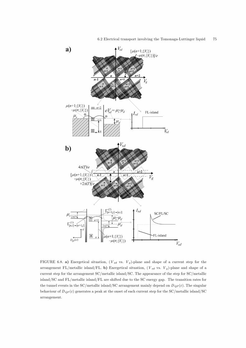
6.2 Electrical transport involving the Tomonaga-Luttinger liquid 75
FIGURE 6.8. a) Energetical situation, (V sd vs. V g )-plane and shape of a current step for the
arrangement FL/metallic island/FL. b) Energetical situation, (V sd vs. V g )-plane and shape of a
current step for the arrangement SC/metallic island/SC. The appearance of the step for SC/metallic
island/SC and FL/metallic island/FL are shifted due to the SC energy gap. The transition rates for
the tunnel events in the SC/metallic island/SC arrangement mainly depend on DQP (ε). The singular
behaviour of DQP (ε) generates a peak at the onset of each current step for the SC/metallic island/SC
arrangement.

76 6. Single-electron charging and quantum wires: suppression of quasi-particle tunneling
FIGURE 6.9. a) On the left, (V sd vs.V g)-plane for a FL/LL/FL arrangement. The transition rates
for a tunnel event in this case are mainly determined τn+1(ε) which leads to the suppression of
transitions to groundstates of the island. On the left, qualitative shape of the current step in the
I/V sd-characteristics. In contrast to the FL/metallic island/FL arrangement a smooth increase of
the step height is apparent. b) On the left, (V sd vs.V g)-plane for a SC/LL/SC arrangement. Similar
to the SC/FL/SC case a currentless band of width 4∆(T )/e is forming along the V g -axis. For com-
parison, the black dashed lines indicate the regular diamonds visible for the arrangement SC/FL/SC
(c.f. Fig. 6.7b). On the right, the shape of the steps in the I/V sd-characteristics. The transition rates
for the SC/LL/SC arrangement depend on both DQP (ε) and τn+1(ε). This leads to a (not necessarily
complete) suppression of the current peak which would occur for a SC/FL/SC arrangement (c.f. Fig.
6.7b). The dotted line indicates the shape of the step for the FL/LL/FL case in (a).

6.3 Single-walled carbon nanotubes connected to superconducting leads: experimental data 77
6.3 Single-walled carbon nanotubes connected to superconducting leads:
experimental data
The predictions of the model discussed in section 6.2 are tested on SWNTs by connecting them electrically
weakly to superconducting Re-electrodes from top as described in section 4.2 and 4.4.1. For the electrical
transport measurements the experimental setup described in section 4.3 has been utilized and cooling
of the samples was performed in both, a liquid helium bath cryostat as well as a 3He/4He-dilution
refrigerator.
In Fig. 6.10 a typical Re electrode structure is shown contacting one individual SWNT bundle. The
room-temperature two-terminal resistance is about 7.9 MΩ, which is in the typical value range of these
types of structures as already stated in section 4.4.1.2.
The electrode lines for all samples were prepared in such a way that also a continuous electrode line
was generated. Electrically contacted at both ends the latter serves as test-line in order to determine the
resistance of the leads to the contacted SWNT and whether the electrodes are still superconducting. At
room-temperature the resistance of the continuous line was measured to be approximately 9.8 kΩ 2.
FIGURE 6.10. SFM image of a Re-electrode structure connecting a thin SWNT bundle (left- and
middle-electrode). Residuals from the lift-off process are visible indicating the more ductile nature of
Re compared to Au or AuPd. Inset: two-terminal resistance vs. temperature of the right continuous
line. At 6.6 K a sharp drop is observed indicating that the electrode lines are indeed superconducting
despite their reduced dimensions.
2The resistivity of Re (19.3 µΩcm) is approximately ten times larger than that of Au (2.24 µΩcm).

78 6. Single-electron charging and quantum wires: suppression of quasi-particle tunneling
FIGURE 6.11. I/V sd -characteristics of three different samples at 4.2 K with differing electrical cou-
pling between SWNT and Re: a) 7.9 MΩ, b) 80 MΩ and c) 100 MΩ room-temperature resistance.
Although step-like features are visible, in none of the curves a well-pronounced peak is observed
which should be due to QP tunneling (c.f. section 6.1.2 and 6.2).
As discussed in section 4.4.1.2 Re in thin films down to 50 nm thickness exhibits a superconducting
transition temperature Tc of about 6.7 K [57]. However, the here generated electrode structures are
only 25 nm in height and considerably reduced in one additional dimension compared to the thin films.
That is, the electrode lines have to be regarded more as thin wires than thin films. Accordingly, if
the electrodes are still superconducting, their critical temperature may be lower due to their reduced
geometric dimensions.
In the inset of Fig. 6.10 the temperature dependence of the resistance of the continuous line is plotted.
At 6.6 K an abrupt drop in the resistance is observed. This significant reduction of the resistance at
a temperature close to the critical temperature of thin films of Re clearly indicates that the electrode
lines are indeed still superconducting in spite of their reduced geometrical dimensions. Remarkably,
the difference to T (film)c is rather small and the superconducting gap at zero temperature is 2∆0 =
3.5kBTc ≈ 1.99 meV [73]. The slight increase of the resistance before Tc is probably due to the enhancedpolycrystalline structure of the Re when evaporated on a cooled surface, as the incident atoms are
immobilized.
The I/Vsd-characteristic at 4.2 K of the sample is plotted in Fig. 6.11a. For comparison, in Fig. 6.11b
and 6.11c the I/Vsd-characteristics of two other samples connecting SWNTs with Re electrodes with
considerably higher room-temperature resistances are shown. The room-temperature resistances are all
considerably higher than the quantum resistance, in particular for the latter two samples, such that
single-electron tunneling is expected at low temperatures. Indeed a step-formation in all three samples
is observed. From the discussion in section 6.2, a peak should accompany the onset of each step in the
I/Vsd-characteristic if the SWNT is in a FL-like state. Apparently, in none of the samples peaks at the
onset of a step can be observed. In particular the high room-temperature resistances of the samples in
Fig. 6.11b and 6.11c, indicate that the absence of the peaks is not due to a insufficiently pronounced
electrically weak coupling of the SWNT and the surrounding electrodes.
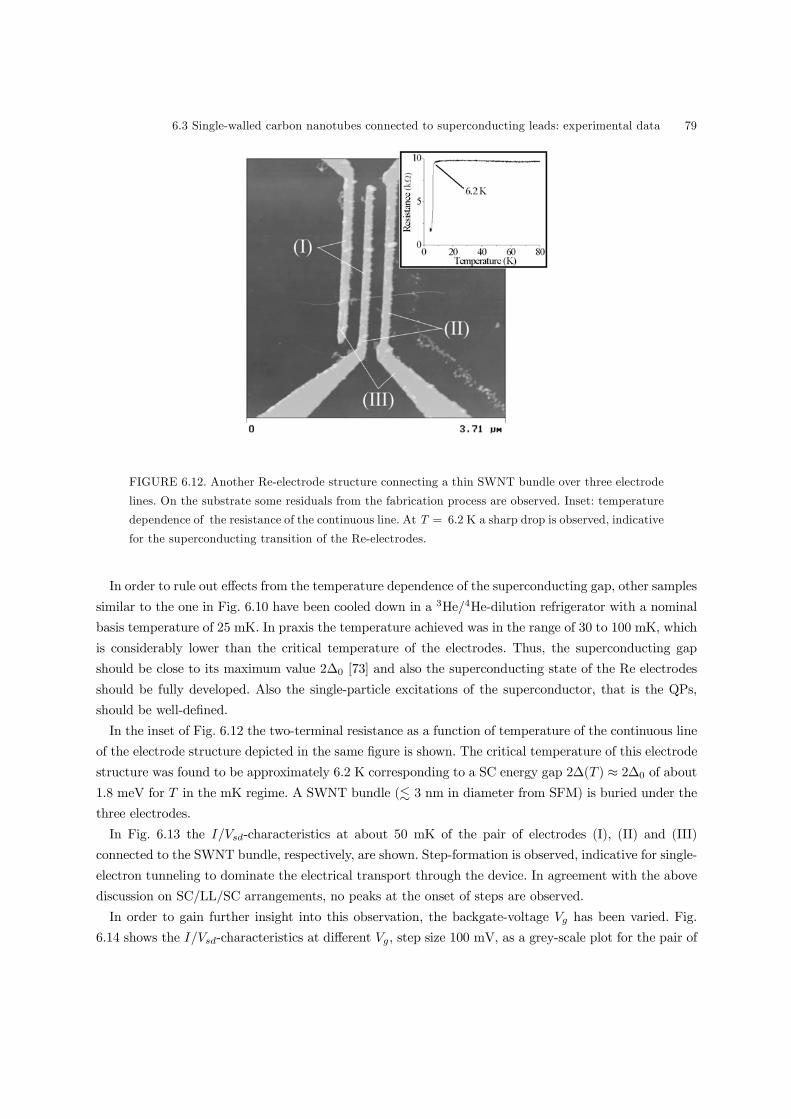
6.3 Single-walled carbon nanotubes connected to superconducting leads: experimental data 79
FIGURE 6.12. Another Re-electrode structure connecting a thin SWNT bundle over three electrode
lines. On the substrate some residuals from the fabrication process are observed. Inset: temperature
dependence of the resistance of the continuous line. At T = 6.2 K a sharp drop is observed, indicative
for the superconducting transition of the Re-electrodes.
In order to rule out effects from the temperature dependence of the superconducting gap, other samples
similar to the one in Fig. 6.10 have been cooled down in a 3He/4He-dilution refrigerator with a nominal
basis temperature of 25 mK. In praxis the temperature achieved was in the range of 30 to 100 mK, which
is considerably lower than the critical temperature of the electrodes. Thus, the superconducting gap
should be close to its maximum value 2∆0 [73] and also the superconducting state of the Re electrodes
should be fully developed. Also the single-particle excitations of the superconductor, that is the QPs,
should be well-defined.
In the inset of Fig. 6.12 the two-terminal resistance as a function of temperature of the continuous line
of the electrode structure depicted in the same figure is shown. The critical temperature of this electrode
structure was found to be approximately 6.2 K corresponding to a SC energy gap 2∆(T ) ≈ 2∆0 of about1.8 meV for T in the mK regime. A SWNT bundle (. 3 nm in diameter from SFM) is buried under the
three electrodes.
In Fig. 6.13 the I/Vsd-characteristics at about 50 mK of the pair of electrodes (I), (II) and (III)
connected to the SWNT bundle, respectively, are shown. Step-formation is observed, indicative for single-
electron tunneling to dominate the electrical transport through the device. In agreement with the above
discussion on SC/LL/SC arrangements, no peaks at the onset of steps are observed.
In order to gain further insight into this observation, the backgate-voltage Vg has been varied. Fig.
6.14 shows the I/Vsd-characteristics at different Vg, step size 100 mV, as a grey-scale plot for the pair of

80 6. Single-electron charging and quantum wires: suppression of quasi-particle tunneling
FIGURE 6.13. I/V sd -characteristics of the electrode pairs (I), (II) and (III) in Fig. 6.12. In all curves
step-like features are observed but no peaks at the onset of the steps are visible.
FIGURE 6.14. Grey-scale plot of the I/V sd -characteristics for different V g of electrode pair (III) in
Fig. 6.12. The stepsize for V g was 100 mV. A currentless band similar to the other two electrode pairs
is observed. Some diamond-like structures are appreciably visible and are indicated by dotted lines
(only some vertical lines are drawn in order to keep clarity). Apparently the diamond-like structures
are not as regular as predicted by the model discussed in section 6.1.2 and 6.2. For better contrast the
”current-height” lines are also plotted. (Dark grey denotes increasing negative, bright grey increasing
positive current.)

6.3 Single-walled carbon nanotubes connected to superconducting leads: experimental data 81
FIGURE 6.15. Re-electrode structure connecting a thin SWNT bundle. On the substrate some resid-
uals from the lift-off process are visible. The superconducting transition temperature of the electrodes
was determined to be about 6.8 K.
contacts (III). Positive current is dark, negative current is bright. Well-pronounced peaks in the current
should be visible as significant dark or white spots within the grey-scale plot.
Apparently, no prominent dark or white spots are observable, indicative for QP tunneling induced
current peaks. Yet, a currentless band of approximately 3.8 mV is visible in the data which coincides
reasonably good to the theoretically predicted width of 4∆0/e ≈ 3.6 mV for the currentless band by themodel discussed in sections 6.1 and 6.2. Also, a diamond-like structure (see white dotted lines as guide
for the eye) is observed which is of relatively irregular shape in both of their ”width” measured relatively
to the Vsd- and the Vg-axis.
A possible reason for this observation could be the likely differences of the LL-like state in the SWNT
compared to a ”pure” LL state of, for example, a linear chain of atoms. The tubular geometry and the
helicity as well as the actual length of the SWNT might lead to these differences.
The data depicted in Fig. 6.14 exemplifies the general qualitative behaviour found for all three pairs
of contacts when varying Vg. The data for the pair of contacts (I) and (II), respectively, are depicted in
Appendix D for completeness.
In order to confirm the observed data so far, another SWNT was measured (Fig. 6.15). The room-
temperature two-terminal resistance of this sample was found to be 1.2 MΩ and Tc to be approximately
6.8 K. Therefore, for this electrode structure 2∆0 = 3.5kBTc ≈ 2.0 meV.

82 6. Single-electron charging and quantum wires: suppression of quasi-particle tunneling
FIGURE 6.16. Grey-scale plot of the I/V sd -characteristics for different V g of the sample shown in
Fig. 6.15. The stepsize for V g was 25 mV. A currentless band of width 3.8 mV coincides quite well
with the predicted value of 4 mV. Some diamond-like structures are indicated by white dotted lines.
Not all vertical white dotted lines have been drawn for clarity. Again the diamond-like structures are
not as regular as predicted by the model discussed in section 6.1.2 and 6.2. The current height-lines
are also plotted for better contrast. In the plot dark grey denotes increasing negative, bright grey
increasing positive current.
In Fig. 6.16 the measured data is depicted in a grey-scale plot. The axis are the source-drain voltage Vsdand the backgate-voltage Vg (step size 25 mV). The currentless band around zero Vsd can be estimated
from the data to be about 3.8 meV which coincidences well with the predicted width of 4∆0/e ≈ 4 mV.As in the data for the other samples, no pronounced current peaks, that is significant dark or white
spots, are apparent within the grey-scale plot. Also the irregular diamond-like structure as found in the
previously presented data is observed. In this sample these patterns happen to be similarly irregular as
the ones shown Fig. 6.14.
In the grey-scale plots depicted, the currentless band was shown to exist. Its appearance and the widths
found in the data are in agreement with the theoretically predictions of the model discussed in section
6.2. Yet, no well-pronounced current peaks, that is dark or white spots in the plot, are observable at any
Vg. This was already indicated by the I/Vsd-characteristics in Fig. 6.11 and 6.13.

6.4 Qualitative comparison of experimental data and model 83
FIGURE 6.17. Output characteristics of electrode pair (II) at backgate-voltages from -3 V to +3 V
in steps of 200 mV. At some V g weakly pronounced peaks (some are indicated by arrow and circle)
are observed at the onset of a current-step. Inset: enlarged view of one of the shallow peaks.
Closer inspection of the I/Vsd-characteristics of the samples, reveals that the I/Vsd-characteristics of all
samples exhibit the same general behaviour. This is exemplified in Fig. 6.17 on the I/Vsd-characteristics
of electrode pair (II) of the sample depicted in Fig. 6.12. The I/Vsd-characteristics are shifted for clarity
with respect to each other and some of the curves show towards higher Vsd current fluctuations which are
attributed to instabilities of the contact region versus time. Further it is observed that at some Vsd and
Vg weakly pronounced peaks (some are indicated by circles and arrows) at the onset of the current-steps
are apparent. In the inset of Fig. 6.17 an enlarged view of one of the shallow peaks is plotted. The
observation of only some shallow current peaks is consistent with the prediction in section 6.2 that if
they are not completely suppressed, at least their height should be considerably lowered. As apparent
from Fig. 6.17, the peaks are that small in height that they are hardly visible in the grey-scale plots
shown above. That the weakly pronounced peaks seem to appear irregularly depending on Vsd and Vg,
coincides with the irregularities observed in the diamond-like structures.
6.4 Qualitative comparison of experimental data and model
In the experimental data shown in section 6.3, the two main features of the SC/LL/SC model discussed in
section 6.2 are observed: a currentless band of a width twice the SC energy gap along the Vg-axis is visible
and suppression, at least in height, of QP tunneling induced current peaks in the I/Vsd-characteristics.
84 6. Single-electron charging and quantum wires: suppression of quasi-particle tunneling
The experimentally observed diamond-like structures in the (Vsd vs. Vg)-plane show irregularities
compared to the theoretical model discussed in section 6.2. The ”width” with respect the Vsd-axis and
the the Vg-axis of the diamond-like structures are varying. Also a variation of the slopes of the border
lines of the these patterns is observed.
In the model the energy difference µ(n+1; Vl)−µ(n; Vl) was assumed to be constant (for simplicity)for all n which generates transport regions of equal widths with respect the Vsd-axis and the the Vg-axis.
However, this condition is usually only quite well fulfilled for metallic-like islands. But in the case of a
correlated 1D electron system, as represented here by the investigated SWNTs, µ(n+1; Vl)−µ(n; Vl)are most likely to vary with the number of electrons on the island and therefore leading to the variation in
the size of the diamond-like structures. Additionally, due to the lack of a superior division of the (Vsd vs.
Vg)-plane for SC/LL/SC-arrangements a higher complexity is introduced already to the pattern which
is observed. The dependence of the electrical transport through the island on the number of charges n,
may in particular lead to the irregular appearance of weakly developed current peaks depending on Vsdand Vg as apparent in Fig. 6.17.
The change of the slopes of the border lines of the transport regions, that is the diamond-like struc-
tures, implies a change in the capacitive couplings (c.f. Fig 6.2). Physically this observation points
towards strong charge redistributions whenever an electron tunnels into the SWNT. Although this seems
reasonable as the SWNT is in a LL-like state, the capacitive coupling to the backgate is not expected
at first sight to be severely affected by these charge redistributions due to its infinite ”size” compared
to the SWNT. At the present stage it is not possible to give simple, qualitative arguments leading to
this behaviour. Further insight could only be provided by a rigorous theoretical treatment which takes
all microscopic parameters of the SWNT (as for example diameter and helicity) and the backgate, e.g.,
details on the crystallinity of the insulating SiO2-layer or the interactions between the SiO2-surface and
the SWNT, which is beyond the scope of the present thesis but should be subject to future investigations.
However, the experimentally observed suppression of QP tunneling induced current peaks in the I/Vsd-
characteristic due to the LL-like properties of the SWNT and the development of a currentless band of
width 2∆(T ) along the Vg-axis, are not affected by the above discussed deviations of the model proposed
in this chapter.
6.5 Concluding remarks
In conclusion, the comparison of the experimental data with the proposed theoretical model, points
towards the principle necessity to consider whether a low-dimensional island (here the SWNT), which is
capacitively (electrically weak) coupled to reservoirs, is in a FL-like or in a LL-like state. Therefore no
suppression of QP tunneling induced current peaks are observed in the measurements in Ref. [74], where
the island is formed by a spherical metal grain with FL-like behaviour.
In contrast, if the island is in a LL-like state, a counterbalance of the QP density of states DQP (ε)
in the superconducting leads and the tunneling density of states τ(²) in the LL can occur. This was
6.5 Concluding remarks 85
observed in the experimental data presented in section 6.3 for the Re/SWNT/Re devices. Therefore, in
total, the experimental observations presented are consistent with the expectation of a LL-like state in
SWNTs at low temperatures. It is noteworthy, that SWNTs may exhibit differences in their excitation
spectrum compared to a ”pure” LL, which is likely to be due to parameters like diameter and/or the
actual structure (helicity).
Within this context, it follows also that the degree of suppression of the current peaks in the I/Vsd-
characteristics depends on how strong the LL-like character of the island is developed. For example, for
MWNTs also signatures of a LL-like state have been observed [39]. However, as MWNTs have a typically
one order of magnitude larger diameter than SWNTs their 1D character is much less pronounced. There-
fore, the development of a LL-like state should be hindered which is supported by other experimental
works [7],[78] and also by theoretical considerations [41] (c.f. also section 3.2.4). In view of the here
presented experiments, the degree of suppression of the QP tunneling induced current peaks, is therefore
likely to be smaller in MWNTs.

86 6. Single-electron charging and quantum wires: suppression of quasi-particle tunneling

7
Electrical Magnetochiral Anisotropy
As discussed in section 2.1, certain CNTs are chiral molecular objects and therefore exist in two forms
that are each other’s mirror image. Many aspects of the CNTs have been explored but their chirality has
hardly been addressed. The main reasons for this are the lack of an enantioselective production process
and the experimental difficulties in addressing the chirality of an individual nanotube and not only its
helicity, which is determined by the pair of integers (n,m).
In this chapter, the charge transport through SWNTs in the presence of a magnetic field parallel to
the tube axis is investigated. A dependence of the resistance that is odd in both the magnetic field and
in the current through the tube is observed in several samples. This effect is ascribed to the chirality of
the nanotube and is called electrical Magnetochiral Anisotropy (eMChA).
Before the discussion of the experimental electrical transport data, a short introduction to the optical
Magnetochiral Anisotropy, the analogy of the eMChA, is given. This is followed by a theoretical consid-
eration proving the principal existence of the eMChA in chiral conductors. Finally, after the discussion of
the experimental data, a simple theoretical model is proposed, which recovers the eMChA on a quantum
mechanical basis.
7.1 Optical Magnetochiral Anisotropy in chiral molecules
The phenomenon of chirality is well known in optics. Chiral molecules, as for example cane sugar, are
(naturally) optically active: the polarization plane of linearly polarized monochromatic light traversing
an aqueous cane sugar solution is rotated perpendicular to its direction of propagation [79], that is, per-
pendicular to its wave vector−→k . Depending on whether the rotation is positive (clock-wise) or negative
(anti-clock-wise) to the incident polarization plane, the optically active material is called dextrorotatory
(D) or levorotatory (L)1, respectively. Similarly, the effect of optical rotation is also observed in crystals
like quartz (SiO2) [80]. In its lattice a kind of corkscrew arrangement can be seen. Therefore, quartz is
a chiral material and exists in two mirror-image forms. The two forms are also called right-handed or
left-handed, depending whether the material is dextrorotatory or levorotatory, respectively. This nomen-
clature has been generalized to all chiral objects, as the two mirror-forms are connected via a parity
operation (c.f. section 2.1). The two forms of the chiral material are termed enantiomers.
Beside the optical activity there is also the magneto-optical activity of materials. This effect occurs
in all materials that have a magnetization, either intrinsic, like ferromagnets, or induced by an external
magnetic field. Examples are transparent iron films (about 10 µm thickness) or gaseous CO2 [81]. Er-
1The expressions dextrorotatory and levorotatory are derived from the Greek words δεξια (dexia) = right, δεξιoς (dexios)
= (to be) right and λαυoς (layos) = wrong, λαθoς (lathos) = error.

88 7. Electrical Magnetochiral Anisotropy
roneously, one could describe magneto-optical activity as the result of magnetically induced chirality of
the material [82]. The Faraday effect is one of the oldest known effects of this type. A linearly polarized
electromagnetic wave experiences a rotation of the polarization vector when traversing a transparent
medium along the direction of a magnetic field. The magnitude of the angle of rotation is proportional
to the magnetic field strength.
In the time period from 1962 to 1984, in several publications [83] a cross-effect between the natural
optical activity and the magneto-optical activity has been predicted which has the ability to distinguish
between the two enantiomeric forms of a chiral material. This cross-effect has been called (optical)
Magnetochiral Anisotropy (MChA). The existence of the MChA can be derived by the expansion of the
dielectric tensor ² of a chiral medium to first order in the−→k -vector of the propagating electromagnetic
wave and the externally applied magnetic field−→B . For gases, liquids, cubic or uniaxial crystals, that is
high symmetry media, the dielectric tensor can be described by [84],[85]
²±(ω) = ²(ω)± αD/L(ω)k ± β(ω)B + γD/L(ω)−→k ·−→B (7.1)
where the +(−)-sign denotes right-(left-) handed circularly polarized electromagnetic waves, which arethe optical eigen-modes of the media. The indices D and L describe right- and left-handed media,
respectively, as already mentioned at the beginning of this chapter. k and B are the absolute values of−→k and
−→B , respectively. The term αD/L(ω)k denotes the natural optical activity and β(ω)B represents
the Faraday effect. The term
γD/L(ω)−→k ·−→B (7.2)
describes the optical MChA. Now it is also apparent why the MChA is an anisotropic effect: the scalar
product−→k ·−→B makes the space anisotropic. The main features of the MChA are (i) the dependence on
the relative orientation of−→k and
−→B , (ii) the dependence on the handedness of the chiral material (enan-
tioselectivity) and (iii) the independence on the polarization state of the propagating electromagnetic
wave.
7.2 Electrical Magnetochiral Anisotropy: symmetry arguments
One of the fundamentals in physics in the microscopic world is the so-called particle-wave dualism. Getting
from macroscopic, bulk materials down to smaller geometric dimensions, the object under investigation
looses its corpuscular and simultaneously gains wave-like character. This dualism is expressed in the
de-Broglie wave-length of any physical object or particle
λdeBroglie =h
p(7.3)
where h is the Planck’s constant and p = |−→p | the total momentum of the particle. Originally, L. de Broglieintroduced (7.3) in 1924 in the way, that with each corpuscular particle of mass m and with momentum−→p = m−→υ a plane wave is classed, which propagates with the velocity −→υ and has the wave length

7.2 Electrical Magnetochiral Anisotropy: symmetry arguments 89
λdeBroglie. However, (7.3) also holds for the relativistic case, in particular also for massless particles.
Therefore (7.3) is of more general validity as initially introduced by L. de Broglie. In consequence, not
only each corpuscular particle is classed with a wave, but also each wave is classed with a corpuscular
particle. For example, an electron can be regarded as a wave and the energy quanta of an electromagnetic
wave (photons) can be regarded to exhibit particle-like properties. Another example is a phonon which
is the energy quantum of the oscillations of for example a crystal lattice.
The dualism leads to the assumption that physical phenomena existing in optics should also exist for
mass-carrying particles. This is in agreement with the fact that the concept of chirality is very general
and by no means restricted to optics. Principally, also thermal or electrical conductors can be chiral.
Chiral electrical conductors are conductors exhibiting a chiral current path. The reason for this can be
of various types: the material may crystallize in a chiral space group, like tellurium, or be composed of
chiral subunits like chiral conducting polymers [86]. Even if the material under consideration is achiral,
it may be formed into a chiral shape as for example a helix. In all these cases, as well as in general, the
physical quantities describing the object must reflect the chiral character. Such kind of physical quantities
ξD/L are defined by changing its sign under a parity operation bP . In other words, the chiral quantity canrepresent either the left-handed (L) or the other the right-handed (D) form of the chiral system which
it is describing: bP ξD = ξL with ξD = −ξL. (7.4)
From a mathematical point of view, if ξD/L is a scalar (function), it is called a pseudo-scalar, if it is a
vectorial quantity it is termed an axial vector.
In the following two sections 7.2.1 and 7.2.2 it will be shown that the existence of the eMChA can be
derived from time- and parity-reversal symmetry. Both, ballistic as well as diffusive charge transport in
chiral objects will be considered.
7.2.1 Ballistic charge transport
In the case of a ballistic conductor, the charge carriers do not suffer from any scattering process. Consid-
ering that the ballistic current density−→j is directly connected to the expectation value of the momentum
vectors−→k of the charge carriers, the following parity and time-reversal symmetries hold, where bP and bT
are the parity and time-reversal operators, respectively,
bP−→B =−→B ; bP−→j = −−→j (7.5)bT−→B = −−→B ; bT−→j = −−→j .
Obviously, an asymmetry regarding these symmetry operations is apparent with respect to the magnetic
field−→B and the current density
−→j . First consider that the resistance R only depends on the magnetic
field. Then, application of (7.5) leads to
bTR³−→B´ = R³−−→B
´= R
³−→B´
(7.6)
bPR³−→B´ = R³−→B´

90 7. Electrical Magnetochiral Anisotropy
where the condition that R is a scalar quantity and therefore invariant under bP and bT has to be takeninto account. Therefore, if the resistance solely depends on the magnetic field, by symmetry only even
powers in−→B are allowed and R
³−→B´may be written as
R³−→B´= R0 + α1
−→B 2 + o
³αn−→B 2n+1
´(7.7)
consisting of the terms R0 which is some invariant part, α1−→B 2 the usual diamagnetism that exists in
any conductor and higher order contributions o³αn−→B 2n+1
´where n is an integer number. The αn’s are
appropriate coefficients.
In contrast to a simple, achiral conductor, as discussed above, in chiral conductors principally all
microscopic transport properties are allowed to depend on the wavevectors−→k of the according particles
[87]. Therefore, the resistance of a ballistic chiral conductor in general depends on−→B and
−→j . Time and
parity-reversal symmetry and invariance of scalar quantities under these symmetry operations require
then for the resistance R³−→B,−→j´
bTR³−→B,−→j ´ = R³−−→B,−−→j
´= R
³−→B,−→j´
(7.8)
bPR³−→B,−→j ´ = R³−→B,−−→j
´= R
³−→B,−→j´.
Based on these symmetry considerations R³−→B,−→j´may be written as
R³−→B,−→j´
= R0 + α1−→B 2 + β1
−→j 2 + γ11
−→j 2 ·−→B 2 + χ
D/L00
−→j ·−→B (7.9)
+o³−→j 2k ·−→B 2r
´+ o
³−→j 2p+1 ·−→B 2q+1
´.
where k, r, p and q are integer numbers. Note that the coefficients of all terms in (7.9) are not necessarily
simple constants, but have no internal dependences on−→j or
−→B .
The linear term χD/L00
−→j ·−→B and the higher order terms o
³−→j 2p+1 ·−→B 2q+1
´with odd power in
−→j and
−→B seem to be not compatible with the requirement of the equalities (7.9) as they are of odd power in
−→j
and−→B . This pretended contradiction is lifted taking the chiral character of the conductor into account:
the corresponding coefficients of the product−→j ·−→B and the higher order terms
−→j 2p+1 ·−→B 2q+1 are chiral
quantities which change sign under bP according to (7.4). Therefore the last term does not contradict therequirement bPR³−→B,−→j ´ = R³−→B,−→j ´ (for a more detailed derivation see Appendix E). The terms
χD/L00
−→j ·−→B + o
³−→j 2p+1 ·−→B 2q+1
´(7.10)
are describing the eMChA. Note the resemblance of this expression with the optical MChA. As for a bal-
listic conductor the situation is equivalent to an electromagnetic wave propagating in an electromagnetic
wave-guide or some transparent dielectric medium, the above symmetry-based derivation could also be
applied in complete analogy to the dielectric tensor instead of the resistance. Apparently, the features of
eMChA are similar to those of the optical MChA: (i) the dependence on the relative orientation of−→j
and−→B , (ii) the dependence on the handedness of the chiral material, that is, enantioselectivity and (iii)

7.2 Electrical Magnetochiral Anisotropy: symmetry arguments 91
the independence of the polarization state of the conducting electrons (e.g. spin-polarized electrons with
their spin parallel to their−→k -vector are analogous to circularly polarized light).
7.2.2 Diffusive charge transport: the Onsager relation
In contrast to the ballistic case, time-reversal symmetry cannot be directly applied to diffusive charge
transport. Diffusion involves elastic and/or inelastic scattering processes of the charge carriers where
the latter leads to Joule’s heating of the conductor. In both cases the current traversing the diffusive
conductor cannot be simply inverted by a time-reversal operation bT as the second law of thermodynamicswould be violated. Therefore diffusion breaks the time-reversal symmetry and one has to use the Onsager
relation [88]. The Onsager relation describes the generalized time-reversal operation for any transport
coefficient σij , as for example electrical or thermal conductivity, close to thermal equilibrium
σik = σ†ki (7.11)
where † denotes the time reversal and the indices i, k the spatial axis. In case the conductor only haselastic scatterers, alternatively the reciprocity relation Rpq,kl= Rkl,pq for the resistance can be used
[61]. The pair of indices p and q denote the contacts used to supply and draw current, k and l denote
the probes used to measure the potential difference. However, this is just a special case of the Onsager
relation and can be derived from the same [89].
Let σik’s represent the coefficients of the electrical conductivity tensor σ and assume first a simple
diffusive conductor, that is σik = σik
³−→B´. Then applying Onsager’s relation yields (the index † is
dropped for simplicity),
σik³−→B´= σki
³−−→B
´. (7.12)
As σ is a tensor, it can be written as the sum of a symmetric tensor s and an asymmetric tensor a.
Therefore, in terms of tensor coefficients it follows
σik³−→B´= sik
³−→B´+ aik
³−→B´. (7.13)
Applying Onsager’s relation to sik³−→B´, one finds sik
³−→B´= sik
³−−→B
´for all i, k due to the symmetry
property of s. Consequently, sik³−→B´has to be an even function in the magnetic field, i.e., only terms
of even power in−→B are allowed. In contrast aik
³−→B´is an asymmetric quantity, such that aik
³−→B´=
−aik³−−→B
´for all i, k which implies that aii
³−→B´= 0 and only off-diagonal elements of a are non-zero.
Therefore, aik³−→B´can only depend on odd powers of
−→B . The parity-reversal operation bPσik ³−→B´ =
σik
³ bP−→B´ = σik
³−→B´leaves sik
³−→B´and aik
³−→B´unaltered and thus σik
³−→B´contains even as well as
odd powers in−→B . But the diagonal elements σii
³−→B´, which describe the longitudinal conductivity, are
only determined by the symmetric part of the conductivity tensor (see Appendix E for more details).
This is equivalent with the statement, that any two-terminal resistance of an achiral conductor can only

92 7. Electrical Magnetochiral Anisotropy
have an even magnetic field dependence. The off-diagonal elements are determined by both, symmetric
and asymmetric part. For example, the Hall-effect can be deduced from aik³−→B´[90].
In the case of a chiral conductor the components of the conductivity tensor read
σik³−→j ,−→B´= sik
³−→j ,−→B´+ aik
³−→j ,−→B´. (7.14)
Then the Onsager relation and the symmetry properties of the components lead to sik³−→j ,−→B´=
sik³−−→j ,−−→B
´and aik
³−→j ,−→B´= −aik
³−−→j ,−−→B
´. As the parity operation requires bPσik ³−→j ,−→B´ =
σik
³−−→j ,−→B
´= σik
³−→j ,−→B´, the allowed dependences of the symmetric and asymmetric part of the
conductivity tensor in−→B and
−→j reduces to
aik³−→j ,−→B´
= a(0)ik + ²
(0)ik
¯−→B¯+ ε
(0)ik
¯−→j¯
(7.15)
+o³−→j 2k ·−→B 2r+1
´+ o
³−→j 2p+1 ·−→B 2q
´,
sik
³−→j ,−→B´
= s(0)ik + α
(1)ik
−→B 2 + β
(1)ik
−→j 2 + κD/Lik,00
−→j ·−→B (7.16)
+o³−→j 2p+1 ·−→B 2q+1
´+ o
³−→j 2k ·−→B 2r
´.
The terms of odd power in−→B and
−→j in the symmetric part seem to contradict the requirement of the
parity operation. As the conductor is chiral, the coefficients of these terms are chiral quantities and have
to transform under parity as given in (7.4) (see also Appendix E). That is for the linear term in−→B and
−→j in (7.16): bPκDik,00 = κLik,00 with κDik,00 = −κLik,00.In the last expression the eMChA κD/Lik,00
−→j · −→B + o
³−→j 2p+1 ·−→B 2q+1
´is recovered, similar to the case
of ballistic charge transport. The first term on the right hand side of (7.16) represents some constant
contribution to the conductivity, which in terms of resistivity would be for example lattice-defects, grain
boundaries etc.. The second term is just the diamagnetic contribution which occurs in all materials.
It is interesting to note that the eMChA is found only in the symmetric part of the conductivity tensor.
In a two-terminal electrical transport measurement, where the longitudinal conductivity is measured, only
the diagonal elements sii³−→j ,−→B´are thus contributing to σii
³−→j ,−→B´(as aii
³−→j ,−→B´= 0). Therefore,
in contrast to a achiral conductor, an odd power dependence in−→B and
−→j is apparent.
Finally, it has to be noted that the above derivation also holds for the resistivity tensor of a chiral
conductor, since ρ = σ−1. In terms of components ρik³−→j ,−→B´≡³σ³−→j ,−→B´´−1
ikand in complete analogy
one finds then for the symmetric part of the resistivity tensor
ρ(sym)ik
³−→j ,−→B´= ρ
(0)ik + %
(1)ik
−→B 2 + χ
D/Lik,00
−→j ·−→B + o
³−→j 2p+1 ·−→B 2q+1
´(7.17)
and again the eMChA terms are discovered (other higher order terms have been omitted for simplicity).
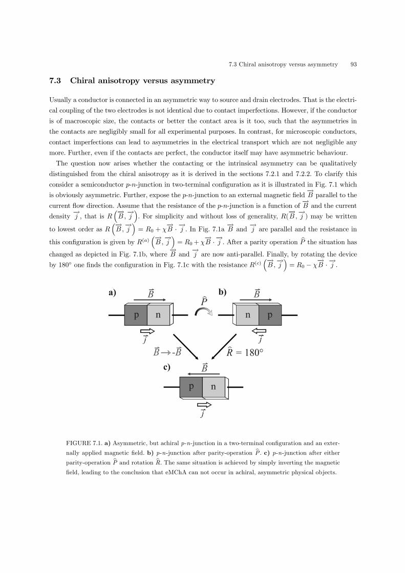
7.3 Chiral anisotropy versus asymmetry 93
7.3 Chiral anisotropy versus asymmetry
Usually a conductor is connected in an asymmetric way to source and drain electrodes. That is the electri-
cal coupling of the two electrodes is not identical due to contact imperfections. However, if the conductor
is of macroscopic size, the contacts or better the contact area is it too, such that the asymmetries in
the contacts are negligibly small for all experimental purposes. In contrast, for microscopic conductors,
contact imperfections can lead to asymmetries in the electrical transport which are not negligible any
more. Further, even if the contacts are perfect, the conductor itself may have asymmetric behaviour.
The question now arises whether the contacting or the intrinsical asymmetry can be qualitatively
distinguished from the chiral anisotropy as it is derived in the sections 7.2.1 and 7.2.2. To clarify this
consider a semiconductor p-n-junction in two-terminal configuration as it is illustrated in Fig. 7.1 which
is obviously asymmetric. Further, expose the p-n-junction to an external magnetic field−→B parallel to the
current flow direction. Assume that the resistance of the p-n-junction is a function of−→B and the current
density−→j , that is R
³−→B,−→j´. For simplicity and without loss of generality, R(
−→B,−→j ) may be written
to lowest order as R³−→B,−→j´= R0 + χ
−→B · −→j . In Fig. 7.1a −→B and
−→j are parallel and the resistance in
this configuration is given by R(a)³−→B,−→j´= R0+χ
−→B ·−→j . After a parity operation bP the situation has
changed as depicted in Fig. 7.1b, where−→B and
−→j are now anti-parallel. Finally, by rotating the device
by 180 one finds the configuration in Fig. 7.1c with the resistance R(c)³−→B,−→j´= R0 − χ
−→B ·−→j .
FIGURE 7.1. a) Asymmetric, but achiral p-n-junction in a two-terminal configuration and an exter-
nally applied magnetic field. b) p-n-junction after parity-operation bP . c) p-n-junction after eitherparity-operation bP and rotation bR. The same situation is achieved by simply inverting the magneticfield, leading to the conclusion that eMChA can not occur in achiral, asymmetric physical objects.

94 7. Electrical Magnetochiral Anisotropy
As neither by bP nor by rotation the resistance of the device is changing, one finds R(a)³−→B,−→j´=
R(c)³−→B,−→j´which is contradictory unless χ = 0. Therefore, any kind of asymmetries in devices, wherever
they may originate from, cannot lead to dependences of the form−→B ·−→j in a two-terminal measurement.
In contrast, replacing the p-n-junction by a chiral object, for example a helix, the coefficient χ ≡ χD/L
is a chiral quantity and behaves as bPχD = χL with χD = −χL and therefore does not contradict theequality R(a)
³−→B,−→j´= R(c)
³−→B,−→j´.
7.4 Experimental data
In this section first the principle experimental technique to measure the eMChA is explained. Then,
charge transport measurements on SWNT samples contacted with electrodes on top are presented. All of
the investigated samples show a high transmission probability between the SWNT and metal contacts.
7.4.1 Experimental technique and set-up
For measuring the electrical Magnetochiral Anisotropy (eMChA), the experimental set-up described
in section 4.3 has to be modified. From (7.9), (7.16) and (7.17) it is apparent, that the two-terminal
resistance of a chiral conductor is anisotropic in the externally applied magnetic field and the traversing
current. Thus the eMChA contribution to the resistance can be extracted if the difference in resistance (or
resistance anisotropy) is measured when the current−→I traversing the SWNT is parallel or anti-parallel
to an externally applied magnetic field−→B . That is,
δR³−→B,−→I´≡ R
³−→B,−→I´−R
³−→B,−−→I
´. (7.18)
As discussed in section 4.2 and 4.4 the contacting area of SWNTs is very sensitive also to changes on the
sub-nanometer scale. Therefore, unintentional, small differences between the two contacts to the SWNT
under investigation may occur. Therefore, a contact-resistance anisotropy may contribute to δR³−→B,−→I´.
However, as shown in section 7.2.1 and 7.2.2, such a contribution can only have an even magnetic field
dependence. In order to eliminate this undesired contribution, the difference in δR³−→B,−→I´for the two
possible orientations is taken which yields, considering (7.17),
∆R³−→B,−→I´≡ δR
³−→B,−→I´− δR
³−−→B,−→I
´= 4χD/L
−→I ·−→B (7.19)
where higher orders in−→I and
−→B have been omitted and indices dropped for simplicity. Therefore, from
the last quantity the MChA coefficient χD/L can be immediately extracted.
In order to obtain δR³−→B,−→I´, the experimental set-up is centred around a V/I-converter (self-made)
and two Lock-In amplifiers (Stanford Instruments, SR 830). In Fig. 7.2 the principle experimental set-up
is shown. The use of Lock-In amplifiers allows a phase-sensitive measurement to be performed as will be
discussed in the following.
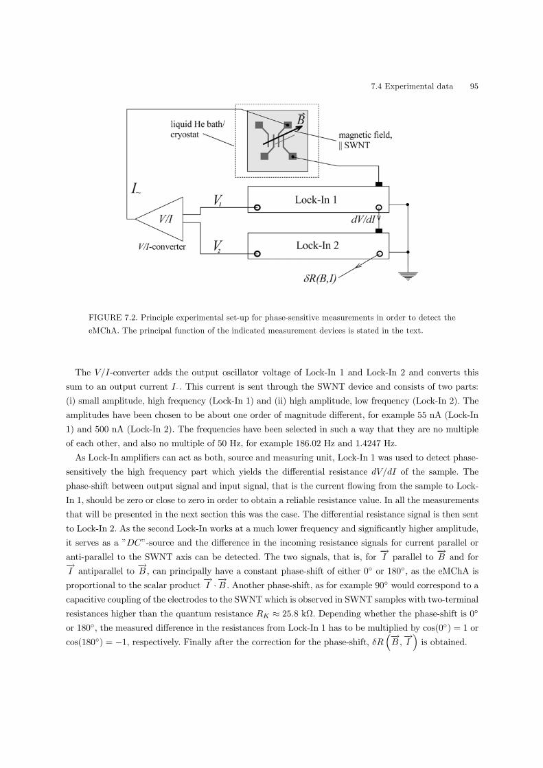
7.4 Experimental data 95
FIGURE 7.2. Principle experimental set-up for phase-sensitive measurements in order to detect the
eMChA. The principal function of the indicated measurement devices is stated in the text.
The V/I-converter adds the output oscillator voltage of Lock-In 1 and Lock-In 2 and converts this
sum to an output current I˜ . This current is sent through the SWNT device and consists of two parts:
(i) small amplitude, high frequency (Lock-In 1) and (ii) high amplitude, low frequency (Lock-In 2). The
amplitudes have been chosen to be about one order of magnitude different, for example 55 nA (Lock-In
1) and 500 nA (Lock-In 2). The frequencies have been selected in such a way that they are no multiple
of each other, and also no multiple of 50 Hz, for example 186.02 Hz and 1.4247 Hz.
As Lock-In amplifiers can act as both, source and measuring unit, Lock-In 1 was used to detect phase-
sensitively the high frequency part which yields the differential resistance dV/dI of the sample. The
phase-shift between output signal and input signal, that is the current flowing from the sample to Lock-
In 1, should be zero or close to zero in order to obtain a reliable resistance value. In all the measurements
that will be presented in the next section this was the case. The differential resistance signal is then sent
to Lock-In 2. As the second Lock-In works at a much lower frequency and significantly higher amplitude,
it serves as a ”DC”-source and the difference in the incoming resistance signals for current parallel or
anti-parallel to the SWNT axis can be detected. The two signals, that is, for−→I parallel to
−→B and for−→
I antiparallel to−→B , can principally have a constant phase-shift of either 0 or 180, as the eMChA is
proportional to the scalar product−→I ·−→B . Another phase-shift, as for example 90 would correspond to a
capacitive coupling of the electrodes to the SWNT which is observed in SWNT samples with two-terminal
resistances higher than the quantum resistance RK ≈ 25.8 kΩ. Depending whether the phase-shift is 0or 180, the measured difference in the resistances from Lock-In 1 has to be multiplied by cos(0) = 1 or
cos(180) = −1, respectively. Finally after the correction for the phase-shift, δR³−→B,−→I´is obtained.

96 7. Electrical Magnetochiral Anisotropy
The main problems during the measurements have been the extremely high electrostatic sensitivity
of the samples and the Lorentz force. The samples had to be protected perfectly against electrostatic
perturbations, otherwise instabilities may occur which may destroy the samples already during mounting
in the cryostat. When brought into the cryostat, the Lorentz force [91] due to the applied magnetic field
in a few cases altered the samples. This effect can be attributed to detachment of the electrodes, if their
adhesion to the substrate’s surface is poor. However, the experimental data presented in the next section
was collected only on absolutely stable SWNT devices.
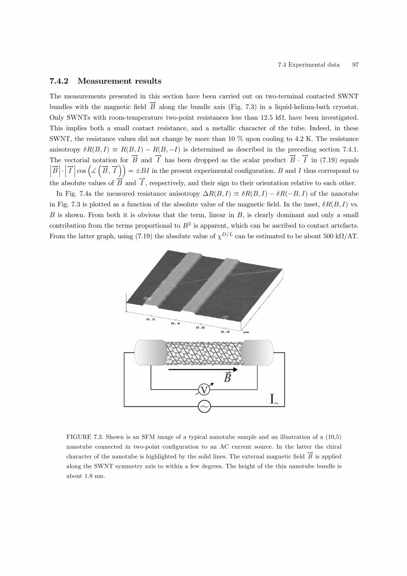
7.4 Experimental data 97
7.4.2 Measurement results
The measurements presented in this section have been carried out on two-terminal contacted SWNT
bundles with the magnetic field−→B along the bundle axis (Fig. 7.3) in a liquid-helium-bath cryostat.
Only SWNTs with room-temperature two-point resistances less than 12.5 kΩ, have been investigated.
This implies both a small contact resistance, and a metallic character of the tube. Indeed, in these
SWNT, the resistance values did not change by more than 10 % upon cooling to 4.2 K. The resistance
anisotropy δR(B, I) ≡ R(B, I) − R(B,−I) is determined as described in the preceding section 7.4.1.The vectorial notation for
−→B and
−→I has been dropped as the scalar product
−→B · −→I in (7.19) equals¯−→
B¯·¯−→I¯cos³]³−→B,−→I´´= ±BI in the present experimental configuration. B and I thus correspond to
the absolute values of−→B and
−→I , respectively, and their sign to their orientation relative to each other.
In Fig. 7.4a the measured resistance anisotropy ∆R(B, I) ≡ δR(B, I) − δR(−B, I) of the nanotubein Fig. 7.3 is plotted as a function of the absolute value of the magnetic field. In the inset, δR(B, I) vs.
B is shown. From both it is obvious that the term, linear in B, is clearly dominant and only a small
contribution from the terms proportional to B2 is apparent, which can be ascribed to contact artefacts.
From the latter graph, using (7.19) the absolute value of χD/L can be estimated to be about 500 kΩ/AT.
FIGURE 7.3. Shown is an SFM image of a typical nanotube sample and an illustration of a (10,5)
nanotube connected in two-point configuration to an AC current source. In the latter the chiral
character of the nanotube is highlighted by the solid lines. The external magnetic field−→B is applied
along the SWNT symmetry axis to within a few degrees. The height of the thin nanotube bundle is
about 1.8 nm.

98 7. Electrical Magnetochiral Anisotropy
B (T)0 5 10 15
∆ R(B
,I) (Ω
)
0
1
2
I = 500 nAT = 4.2 K
B (T)-20 -10 0 10 20
δ R(B
,I) (Ω
)-5
-4
-3 η > 0
FIGURE 7.4. Measured resistance anisotropy ∆R(B,I ) vs. B of the SWNT sample in Fig. 7.3 at
I = 500 nA and T = 4.2 K. In the inset δR(B,I ) vs. B is shown. The linear term in the eMChA
determines the shape of the curve and only small contributions from higher order terms are present.
The eMChA slope can be defined as
η ≡ limB→0
∂
∂B∆R(B, I) (7.20)
which in the sample depicted in Fig. 7.4 yields η > 0. At a given current and field orientation, the two
signs of η are assigned to the two handedness of the SWNTs. Note, that it is not possible to determine
with the experimental setup utilized here, which sign corresponds to which handedness. Thus the sign of η
represents the relative handedness of the investigated SWNT sample. In order to get the real handedness
of the SWNT, either an independent experimental identification, or a rigorous theoretical assignment is
required. However, it should be noted that the clear observation of eMChA proves that charge transport
through CNTs is sensitive to chirality, and therefore must have a three-dimensional character.
In view of the different molecular structures present among the investigated SWNTs (c.f. section
2.1), the eMChA cannot be expected to be the same for all tubes. Fig. 7.5 shows the experimentally
determined δR(B, I) (inset) and ∆R(B, I) for another SWNT. The results for δR(B, I) at fields below
7 T are mostly dominated by quadratic terms in B and no clear linear dependence can be seen. For
higher fields, asymmetry and additional structures can be observed. Upon evaluating ∆R(B, I), the odd
B-dependence characteristic of eMChA appears. At low magnetic field, the linear term is dominant with
an eMChA slope η < 0.
With increasing field, higher odd terms are contributing to the eMChA. The additional structure at
|B| > 8 T probably originates from resonant contributions to the eMChA which are not taken into

7.4 Experimental data 99
B (T)0 4 8 12 16
∆R(B
,I) ( Ω
)
-16
-8
0
8
B (T)-10 0 10
δ R(B
,I) (Ω
)
-70
-60
I = 300 nAT = 4.2 K
η < 0
FIGURE 7.5. Inset δR(B,I ) vs. B for another SWNT at I = 300 nA and T = 4.2 K. The result is
asymmetric in B but at low magnetic field strengths it is still dominated by contributions quadratic in
B. Main figure: ∆R(B,I ) as a function of B. At low magnetic fields (. 5-6 T) the linear contributionto the eMChA is dominant with η < 0. The higher order terms (B 3, B 5,...) start to be important at
increasing fields. The structure at high field may be caused by resonant contributions to the eMChA.
account in the derivation of (7.9) and (7.17) in section 7.2.1 and 7.2.2, respectively. The nature of such
resonances is unclear at this moment, but similar behaviour for δR(B, I) was observed in several other
tubes. However, the resonances can not originate from the Aharanov-Bohm effect, because considerably
higher magnetic fields (up to several 100 T) would be necessary due to the SWNTs small diameter.
As discussed in section 2.1, the so-called armchair and zigzag SWNTs are special classes of nanotubes
that are not chiral. Therefore, no eMChA should be observable in such tubes. In Fig. 7.6 the difference
in resistance δR(B, I) of such a SWNT sample is shown. Upon analysis, the linear contribution turns
out to be about (50 ± 100) kΩ/AT. This means that within the experimental uncertainty, this particularSWNT does not show eMChA and therefore is most likely of an achiral type. Whether this SWNT is an
armchair or a zigzag type cannot be drawn from the experimental data.
During the studies several SWNT samples with different eMChA slope η have been measured. In Fig.
7.7 a histogram is shown in which the number of tubes with a certain sign of η, that is the relative
handedness, is depicted. Five SWNTs with η < 0, four tubes with η > 0 and only one tube with η = 0
have been found. On the basis of SFM data of each of the investigated SWNTs, the diameters can be
estimated to be between 1.0 and 1.4 nm. Within this diameter range, using (2.2) and (2.3), 50 possible
pairs of indices (n,m) can be found. Among these are 3 armchair and 5 zigzag nanotubes, of which 3 and 1,
respectively, are metallic. Out of the chiral nanotubes 12 are metallic, but as they are doubly-degenerate

100 7. Electrical Magnetochiral Anisotropy
B (T)-15 -10 -5 0 5 10 15
δ R(B
,I) (Ω
)
20
22
24I = 500 nAT = 4.2 K
η = 0
FIGURE 7.6. eMChA result of a particular SWNT. Shown is δR(B,I ) as a function of B at I = 500
nA and T = 4.2 K. The dotted line is a fit from which the magnitude of the term linear in B is
estimated to be (50 ± 100) kΩ/AT.
-1 0 +1
occurence of relative handedness
sign(η5 1 4
No.
of S
WN
Ts
0
1
2
3
4
5
)
FIGURE 7.7. Histogram showing the relative handedness sign(η) of the samples investigated. The
relative abundance are in agreement with theoretical considerations.
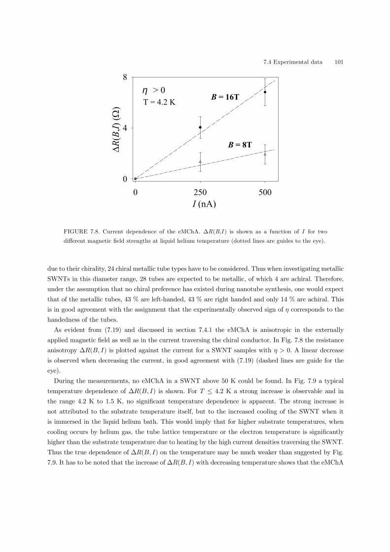
7.4 Experimental data 101
I (nA)0 250 500
∆R(B
,I ) (Ω
)
0
4
8
B = 8T
B = 16TT = 4.2 Kη > 0
FIGURE 7.8. Current dependence of the eMChA. ∆R(B,I ) is shown as a function of I for two
different magnetic field strengths at liquid helium temperature (dotted lines are guides to the eye).
due to their chirality, 24 chiral metallic tube types have to be considered. Thus when investigating metallic
SWNTs in this diameter range, 28 tubes are expected to be metallic, of which 4 are achiral. Therefore,
under the assumption that no chiral preference has existed during nanotube synthesis, one would expect
that of the metallic tubes, 43 % are left-handed, 43 % are right handed and only 14 % are achiral. This
is in good agreement with the assignment that the experimentally observed sign of η corresponds to the
handedness of the tubes.
As evident from (7.19) and discussed in section 7.4.1 the eMChA is anisotropic in the externally
applied magnetic field as well as in the current traversing the chiral conductor. In Fig. 7.8 the resistance
anisotropy ∆R(B, I) is plotted against the current for a SWNT samples with η > 0. A linear decrease
is observed when decreasing the current, in good agreement with (7.19) (dashed lines are guide for the
eye).
During the measurements, no eMChA in a SWNT above 50 K could be found. In Fig. 7.9 a typical
temperature dependence of ∆R(B, I) is shown. For T ≤ 4.2 K a strong increase is observable and in
the range 4.2 K to 1.5 K, no significant temperature dependence is apparent. The strong increase is
not attributed to the substrate temperature itself, but to the increased cooling of the SWNT when it
is immersed in the liquid helium bath. This would imply that for higher substrate temperatures, when
cooling occurs by helium gas, the tube lattice temperature or the electron temperature is significantly
higher than the substrate temperature due to heating by the high current densities traversing the SWNT.
Thus the true dependence of ∆R(B, I) on the temperature may be much weaker than suggested by Fig.
7.9. It has to be noted that the increase of ∆R(B, I) with decreasing temperature shows that the eMChA

102 7. Electrical Magnetochiral Anisotropy
T (K)5 10
∆R(B
,I) ( Ω
)
5
10
15
20
25
B = 14 T
I = 350 nAη < 0
FIGURE 7.9. Temperature dependence of the eMChA. ∆R(B,I ) is plotted as a function of temper-
ature at B = 14 T and I = 350 nA. Temperatures above 4.2 K were obtained by gas cooling, the
others by liquid helium cooling. The dotted line is a guide to the eye.
is not some hot-electron effect, as one might associate with a current dependent resistance, but an intrinsic
contribution of chirality to magnetotransport.
From the experimental data presented in this section, the microscopic origin of the observed eMChA
cannot be determined. Only qualitative arguments can be given in order to elucidate possible mechanisms
at the present stage.
The classical magnetic self-field effect [10] is one imaginable mechanism which can lead to eMChA. For
an estimation of this effect consider the SWNT to be modeled by a conducting helix of the same size.
A current I flowing through the helix will generate an axial magnetic field Baxial = χD/LclassicalI which is
seen by each charge carrier. The parameter χD/L depends on the actual geometry (handedness, number
of turns, length) of the model helix. Applying an external magnetic field Bext in parallel to the helix
yields the effective magnetic field Beff = Baxial ± Bext acts on each charge carrier ((+)-sign for Baxialparallel to Bext and (−)-sign otherwise). Obviously, a difference in the resistance of the helix for differentrelative orientations of the magnetic fields is apparent. It is easy to show [10] that this effect leads to a
term 2χD/LclassicalI ·Bext in the resistance of the helix, which is just the eMChA. Following this analysis of
the experimental data, χD/Lclassical can be estimated to be smaller 5 kΩ/AT for the SWNT-diameter range
(about 0.6 nm) in the present experiments, which is too small to explain the observed effects. However,

7.5 The free electron on a helix - a theoretical model 103
the model of a helix is not unsuitable to obtain informations on the microscopic mechanism if a quantum
mechanical treatment of the helix is performed as it will be shown in section 7.5.
Another possible origin of the eMChA could be scattering by chiral objects, like electron-electron,
electron-phonon, electron-defect or electron-twiston scattering. In view of the observed temperature de-
pendence, electron-phonon scattering is ruled out. An interpretation in terms of electron-twiston scat-
tering would be consistent with the observed temperature dependence of the eMChA as twistons are
chiral CNT lattice deformations [93]. As discussed in section 3.3.3 electron-electron correlations become
important to electronic transport [6] at low temperatures. A chiral electron-electron scattering would,
similar to the electron-twiston scattering process, be consistent with the observed results. Alternatively,
the electron-electron correlation may reduce screening, so that electron-defect scattering becomes more
important. However, in all cases, increasing eMChA with decreasing temperature is to be expected.
The above examples show that a variety of microscopic mechanism for the existence of the eMChA
in SWNTs are possible. Which of them is the dominating one is, as already mentioned, not clear, which
should be subject of future investigations in this field. However, the here presented electrical transport
measurements on SWNTs show that eMChA clearly exists in SWNTs and implies a helicoidal component
of the current path along the SWNT.
7.5 The free electron on a helix - a theoretical model
In this section the free electron on a helix as a simple analytical, quantum mechanical model of a
molecular chiral conductor, like a CNT, is considered. The focus is on diffusive electronic transport
due to achiral scatterers, and ballistic transport through a helix between two achiral contacts. The
considerations are restricted to magnetic fields for which the cyclotron radius of a free electron is large
compared to the helix radius and all electron-electron interaction effects other than those leading to mass
renormalization and scattering are neglected. Restriction to the cylindrical surface of a CNT allows one
to treat the problem in two dimensions. If in addition the two degrees of freedom are correlated, as in
the case of a helix, one finds a one-dimensional description of the problem [94]. Although the reduction
in dimensions facilitates some theoretical considerations, it also inhibits others. An adaptation from
the point of view in terms of dimensionality will be necessary. The quasi-one-dimensional description is
suitable in obtaining qualitative statements on the diffusive transport. To calculate the conductance for
ballistic transport through a helix between bulk, 3D achiral contacts, a three-dimensional approach is
necessary. In both cases, ballistic and diffusive electrical transport, a dependence linearly on the current
and the magnetic field and on the handedness of the helix are found, corresponding to eMChA. These
results agree qualitatively with the experimentally observed eMChA in SWNTs and are compared in
section 7.5.3 also quantitatively with the experimental data in section 7.4. For more details on these
calculations refer to Appendix F.
In Fig. 7.10 the correspondence between a chiral single-wall nanotube and the proposed helix model
is shown.

104 7. Electrical Magnetochiral Anisotropy
FIGURE 7.10. Correspondence between a chiral carbon nanotube and a helix. The radius a, the
pitch p = (2πb)−1 and the winding angle for both are drawn in. In the experiments typical values
for a and b are 0.6 nm and 0.24 nm, respectively. The number of turns N depends on the length of
the SWNT (helix).
7.5.1 Diffusive transport
The Hamiltonian of a free electron with mass m which is restrained to move on a helix of N turns with a
radius a and a pitch p = (2πb)−1, in the presence of a static magnetic field Bbz (pointing along the helix)reads in the symmetric gauge [94]
bH = − ~2
2m(a2 + b2)
∂2
∂ϕ2− i~ q
2m
a2
a2 + b2B
∂
∂ϕ+q2a2
8mB2. (7.21)
The simplest possible case of an electron moving in a given direction on the helix is considered. The
ansatz for its wavefunction is Ψ (ϕ) = C exp(ikϕ). For cyclic boundary conditions Ψ(ϕ = 0) = Ψ(ϕ =
2πN) is imposed, from which follows k = kn = n/N , (n integer). The requirement of orthogonality leads
to the wavefunction Ψn (ϕ) =√2πbN
−1exp (inϕ/N) . This state carriers a current jz,n in the bz direction
[94]
jz,n =q
m(Ψ∗npzΨn −ΨnpzΨ∗n) =
q~nπmN2(a2 + b2)
. (7.22)
The energy eigenvalues can now be obtained by applying Ψn (ϕ) to (7.21) and use of (7.22) leading to
En =~2n2
2mN2(a2 + b2)+qn~2mN
a2
a2 + b2B +
q2a2
8mB2. (7.23)
In this expression, three contributions can be recognized: a zero-field energy Ezf,n ≡ ~2n22mN2(a2+b2) , a
magnetochiral-anisotropy energy EeMChA,n ≡ qn~2mN
a2
a2+b2B = (πN/2)a2jz,nB and a diamagnetic energy
Edia ≡ q2a2
8m B2. That is, in the energy eigenvalues the interaction of the electron with the external

7.5 The free electron on a helix - a theoretical model 105
magnetic field is already apparent. The electronic density of states gn ≡¯(En+1 −En)−1
¯for large n,
taken into account spin degeneracy, is given by
g(En) ≈ |n|Ezf,n
µ1− EeMChA,n
2Ezf,n
¶. (7.24)
In the case of diffusive transport the longitudinal conductivity σ, which has been measured as described
in section 7.4.1, is calculated in the framework of the Boltzmannn transport formalism, using a constant
relaxation time approximation [92] and taking into account the restricted motion of the electron on the
helix:
σij = q2Xn
hviin hvjin∂f(En)
∂Enτ (7.25)
with f(En) being the Fermi distribution, τ the relaxation time and hviin the expectation value of thei-th component of the velocity operators. For the latter ones it is found
hvzin =b
ahvϕin =
~bnmN(a2 + b2)
+qa2b
2m(a2 + b2)B (7.26)
where the correlation between hvϕin and hvzin, as expressed by (7.26), results from the helicoidal motion.The longitudinal conductivity is given by σzz. In order to determine σzz the sum in (7.25) is converted into
an energy integral. The derivative of the Fermi function f(En) yields a Gaussian like function centered
at E = EF . For temperatures for which kBT ¿ E −EF the main contribution to the integration comesfrom the Fermi-energy. Thus, the longitudinal conductivity reads
σ(jz, B) ≈ q2τ
kBThvzi2F g(EF ) ≈ q2τ
kBT
2b2 |nF |m (a2 + b2)
(7.27)
×µ1 +
EeMChA,n
NEzf,nF+
a2Edia(a2 + b2)Ezf,nF
¶µ1− EeMChA,nF
2Ezf,nF
¶leading in consideration of the dominating terms to an eMChA contribution in the diffusive regime,
ξdif ≡σ(jz, B)− σ(−jz, B)σ(jz, B) + σ(−jz, B) ≈
EeMChA,nF
2Ezf,nF≈ πNa2jz,nFB
4Ezf,nF(7.28)
Note, that the term proportional to Edia on the right hand side of (7.27) describes the quadratic
magneto-resistance that occurs in all conductors. In combination with the magnetic self-field inherent to
all current-carrying chiral conductors [92], this also leads to eMChA, as demonstrated in Ref. [10].
7.5.2 Ballistic transport
In the case of ballistic transport along the helix at zero temperature, the conductance G is given by
G =¡e2/h
¢Pi Ti (c.f. section 3.1.1). In the case of perfect transmission, T = 1 and for one spin-
degenerate conducting channelG = 2e2/h. Recently, de Picciotto et al. have shown that in a four-terminal
measurement on a ballistic system there is no influence of an externally applied magnetic field on the
charge transport [22]. Therefore, charge transport on a ballistic helix cannot show any eMChA and in

106 7. Electrical Magnetochiral Anisotropy
FIGURE 7.11. A ballistically conducting helix connected to two reservoirs in two-terminal config-
uration. A current I is driven through the helix with an in parallel applied magnetic field. The
handedness of the helicoidal motion of charge carriers in the reservoirs is opposite to the one of the
helix giving rise to the eMChA.
an ideal four-terminal resistance measurement no eMChA will be detected. However, in a two-terminal
resistance measurement in the ballistic regime, eMChA is possible, even for ideal contacts as discussed
below.
The electronic wavefunctions Φ in the achiral contact material will consist of a cyclotron component
around the magnetic field direction, and a plane wave component along the magnetic field direction. Such
a motion is helicoidal, and it will be intuitively clear that the transmission probability of an electron from
the helix into the contact region Th→c will depend on the relative handedness of the contact wavefunctions
and the helix. Therefore, eMChA in the ballistic regime can be basically regarded as an interface effect
between the contact region and the ballistic helix. The resulting two-terminal conductance will be given
by G ≈ 2q2
h Tc→hTh→c where we have omitted interference terms between reflected waves at the two
ends of the helix [95]. If interference effects would be taken into account, the eigen-states would become
linear combinations of states moving parallel and anti-parallel to the magnetic field. As these states
have opposite contributions to the eMChA, an increase as well as an decrease in the eMChA of the
ballistic transport would be possible. In Fig. 7.11 the case of opposite relative handedness of the contact
wavefunction and the helix is illustrated.
To evaluate Tc→hTh→c, the problem has to be treated in three dimensions in order to take the finite
radial extension of the wavefunction in the contact and on the helix into account. Pictorially, the electron
can be thought to move along a three-dimensional (section area ∼ d2) helicoidal path on a cylinder withradius a. Since a free electron is described, a separation ansatz may be used to approximate the electron
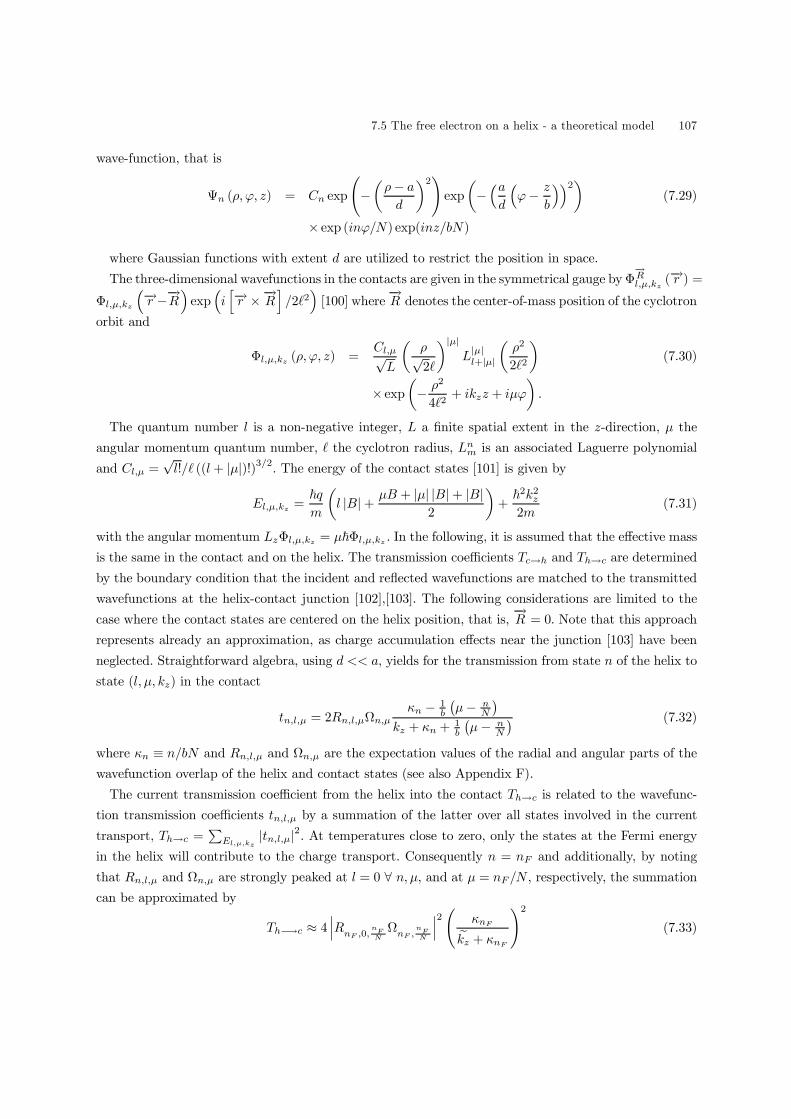
7.5 The free electron on a helix - a theoretical model 107
wave-function, that is
Ψn (ρ,ϕ, z) = Cn exp
Ã−µρ− ad
¶2!exp
µ−³ad
³ϕ− z
b
´´2¶(7.29)
× exp (inϕ/N) exp(inz/bN)
where Gaussian functions with extent d are utilized to restrict the position in space.
The three-dimensional wavefunctions in the contacts are given in the symmetrical gauge byΦ−→Rl,µ,kz
(−→r ) =Φl,µ,kz
³−→r −−→R´ exp³i h−→r ×−→Ri /2`2´ [100] where −→R denotes the center-of-mass position of the cyclotronorbit and
Φl,µ,kz (ρ,ϕ, z) =Cl,µ√L
µρ√2`
¶|µ|L|µ|l+|µ|
µρ2
2`2
¶(7.30)
× expµ− ρ2
4`2+ ikzz + iµϕ
¶.
The quantum number l is a non-negative integer, L a finite spatial extent in the z-direction, µ the
angular momentum quantum number, ` the cyclotron radius, Lnm is an associated Laguerre polynomial
and Cl,µ =√l!/` ((l + |µ|)!)3/2. The energy of the contact states [101] is given by
El,µ,kz =~qm
µl |B|+ µB + |µ| |B|+ |B|
2
¶+~2k2z2m
(7.31)
with the angular momentum LzΦl,µ,kz = µ~Φl,µ,kz . In the following, it is assumed that the effective massis the same in the contact and on the helix. The transmission coefficients Tc→h and Th→c are determined
by the boundary condition that the incident and reflected wavefunctions are matched to the transmitted
wavefunctions at the helix-contact junction [102],[103]. The following considerations are limited to the
case where the contact states are centered on the helix position, that is,−→R = 0. Note that this approach
represents already an approximation, as charge accumulation effects near the junction [103] have been
neglected. Straightforward algebra, using d << a, yields for the transmission from state n of the helix to
state (l, µ, kz) in the contact
tn,l,µ = 2Rn,l,µΩn,µκn − 1
b
¡µ− n
N
¢kz + κn +
1b
¡µ− n
N
¢ (7.32)
where κn ≡ n/bN and Rn,l,µ and Ωn,µ are the expectation values of the radial and angular parts of the
wavefunction overlap of the helix and contact states (see also Appendix F).
The current transmission coefficient from the helix into the contact Th→c is related to the wavefunc-
tion transmission coefficients tn,l,µ by a summation of the latter over all states involved in the current
transport, Th→c =PEl,µ,kz
|tn,l,µ|2. At temperatures close to zero, only the states at the Fermi energyin the helix will contribute to the charge transport. Consequently n = nF and additionally, by noting
that Rn,l,µ and Ωn,µ are strongly peaked at l = 0 ∀ n, µ, and at µ = nF/N , respectively, the summationcan be approximated by
Th−→c ≈ 4¯RnF ,0,
nFNΩnF ,
nFN
¯2Ã κnFekz + κnF
!2(7.33)

108 7. Electrical Magnetochiral Anisotropy
where
ekz ≡ ±r2m
~2
µEF − ~q
m
µB + |µ| |B|+ |B|2
¶1/2(7.34)
≈ kF
µ1− ~q
4mEF
nFB + |nF | |B|+N |B|N
¶with kF ≡ ±
p2mEF /~2 the zero field Fermi wavevector in the contact.
The current transmission coefficient from the contact into the helix Tc→h is calculated analogously. The
main difference is that one has to sum over all reflected waves in the contact. Orthonormality properties,
angular momentum conservation, the considerable difference in the spatial extent of the contact- and
the helix-wavefunction and energy conservation have been used in order to determine the dominant
contribution. For the total transmission coefficient T ≡ Th→cTc→hone finds
T ≈ 16¯RnF ,0,
nFNΩnF ,
nFN
¯4 ekz2κ2nF³ ekz + κnF
´4+ 1
4b2
³ ekz + κnF
´2 . (7.35)
At small magnetic fields and κnF ≈ kF (7.35) yields
T ≈¯RnF ,0,
nFNΩnF ,
nFN
¯4(7.36)
×Ã1− 1
32 (bkF )2
~qmEF
nFB + |nF | |B|+N |B|N
!
leading to the eMChA contribution
ξbal ≡G(I,B)−G(−I,B)G(I,B) +G(−I,B) ≈
−132 (bkF )
2
~qmEF
nFB
N(7.37)
= −a2 + b2
a2EeMChA
16 (bkF )2EF
Similar expressions can be found for different relative sizes of κnF and ekz.7.5.3 Comparison to experiment
The model of a free electron on a helix is a simplified description of a SWNT. In the following its
predictions derived in section 7.5.1 and 7.5.2 are compared to the experimental results obtained on
SWNTs in section 7.4.2.
The typical values for parameters of the experimentally investigated SWNTs are a radius a = 0.6 nm
and a length of 180 nm (distance between source- and drain-electrode). With a inverse pitch p−1 = 2πb =
1.5 nm the number of turns N of the corresponding helix (c.f. Fig. 7.10) is thus equal to 120. The square
of the size of a carbon π-orbital, 0.25 Å2, is taken for d2.
For a helix that corresponds to a metallic SWNT of this size, one finds for the Fermi energy EF ≈ 2.9·10−19J [104], from which utilizing Ezf,nF ≡ ~2n2F
2mN2(a2+b2) , the quantum number nF = 535 and the

7.6 Concluding remarks 109
corresponding Fermi-wavevector κnF = nF /bN ≈ 18.6 · 109 m−1 can be deduced. The large value of nFjustifies the Boltzmann approach that has been used in the section 7.5.1. For a gold contact, the Fermi
energy EF is approximately 1 ·10−18 J [105] and thus |kF | =p2mEF/~2 = 13 · 109 m−1.
Thus (7.37) leads to ξbal/B ≈ 3 · 10−7T−1at a current of 2jz,nF = 1 µA and (7.28) yields the valueξdif/B ≈ 6 · 10−5T−1 at the same current. For realistic parameters, therefore, the predicted ξdif/B is
orders of magnitude larger than ξbal/B. Experimentally ξexp/B ≈ 10−4 T−1at a current of j = 0.3
µA was observed for metallic SWNTs. This is in reasonable agreement with the predicted ξdif/B. It
should however be noted that in the shown electrical transport measurements, no significant temperature
dependence of the conductance, and values close to 4e2/h were observed, suggesting predominantly
ballistic transport. On the other hand, a decrease of eMChA with increasing temperature was observed.
The prediction of a significantly smaller eMChA for ballistic transport than for diffusive transport would
be consistent with this, as transport in SWNT is believed to be ballistic at room temperature down
to intermediate temperatures, but diffusive at low temperatures due to electron-electron correlations
[6],[106]. It is noteworthy that also other results suggest SWNTs to be ballistic down to 4 K [95].
Miyamoto et al. [92] calculated that for large carbon nanotubes the circular component of the diffusive
current is vanishing due to the high in-plane conductivity in graphite. However, like in the present section,
only achiral scatterers have been considered. Chiral scatterers in SWNTs as for example twistons [93]
will also lead to eMChA, analogous to what was shown for screw dislocations in metals [10].
7.6 Concluding remarks
In this chapter the presented experimental data showed the existence of the eMChA in SWNTs. The
experimental studies were performed on several samples and revealed that the amount of SWNTs with
opposite (relative) handedness is approximately the same. This implies that the production process of
SWNTs is not enantioselective. Furthermore the temperature dependence of the eMChA was measured,
showing an increase of the eMChA with decreasing temperature.
In order to obtain information on the physical mechanism in charge transport leading to the eMChA in
SWNTs, the theoretical model of a free electron on a helix [94] has been extended and treated quantum
mechanically. From the comparison of the experimental data and the theoretical model a reasonably
good agreement for the case of diffusive charge transport was found. This coincidence indicates that
scattering on chiral defects, as for example twistons or chiral electron-electron scattering, is the origin of
the eMChA and is consistent with the observed temperature dependence.

110 7. Electrical Magnetochiral Anisotropy
8
Summary
Single-walled carbon nanotubes (SWNTs) are one of the most interesting and fascinating molecular
structures known with exceptional and a rich variety of electronic properties: Depending on the helical
character of the SWNT, they can be either metallic or semiconducting. In particular some SWNTs are
also real chiral molecules, whereas the remaining type of tubes are achiral, which is a consequence of the
interplay of the six-fold symmetry of the carbon-lattice and the helical symmetry of the respective type of
tube. Moreover, at room temperature SWNTs are observed to be ballistic conductors whereas Luttinger-
liquid-like indications are found towards lower temperature, as a consequence of the one-dimensional
electronic nature of the SWNTs.
The present thesis was motivated by the rich variety of physical effects observed in the charge transport
which, however, obey the necessity for further investigations. The scope of the thesis comprises the
experimental investigation of
(i) the influence of electrodes at floating potential electrically coupled to the SWNT on the ballistic
transport properties
(ii) the excitation spectrum due to the Luttinger-liquid properties probed with the aid of superconduct-
ing leads and
(iii) the influence of the chiral character of SWNTs on magnetotransport properties.
In order to perform the electrical transport experiments first an appropriate way of contacting the
SWNTs had to be developed. According to this, contacting with various metals has been investigated.
As contacting procedure standard electron-beam-lithographical techniques have been used: A strong elec-
trical coupling to the SWNTs could be achieved by contacting from top with gold palladium electrodes,
minimizing side effects, like single-electron tunneling due to high tunneling barriers between metal and
SWNT. This way of contacting has been found to be most suitable for the exploration of the influence
of electrodes at floating potential and of the chiral character of SWNTs on the electrical transport.
In order to probe the Luttinger-liquid properties of the SWNTs at low temperature, contacting from
top using the superconductor Rhenium has been found to fulfill the experimental requirements. A weak
electrical coupling to the SWNTs was achieved such that tunneling of single superconductor quasi-
particles could be utilized as probing tool.
SWNTs were contacted in three-terminal configuration where the middle electrode was at floating
potential, that is, no current was flowing through the latter. The experimental results at room temper-
ature were interpreted in the framework of the Landauer-Büttiker formalism, modeling the SWNT by a
ballistic conductor with two spin-degenerated channels and assuming that the middle electrodes acts as
a phase randomizing scatterer. The theoretical results were found to be consistent with the experimental

112 8. Summary
data observed, leading to the existence of a phase-coherent and a non-coherent part of the total current
traversing the SWNT.
At temperatures in the mK regime, the suppression of quasi-particle tunneling from superconducting
Re leads into the SWNT could be observed in the current/voltage-characteristics. The suppression was
found to be not always complete such that partially shallow peaks in the current voltage characteristics
could be found. A simple theoretical model for the superconductor/SWNT/superconductor arrangement
was developed assuming the SWNT to be a Luttinger liquid: Within this model, the suppression of current
peaks is related to the interplay of the tunneling density of states of the SWNTs and the quasi-particle
density of states of the superconductor leads connected. The main features of the model could be found
in the experimental data presented, such that based on this model and the experimental observation,
the Luttinger—liquid-like nature of the SWNTs is clearly indicated. In consequence the interpretation of
previous works on SWNTs, connected to normal metal leads showing single-electron tunneling, in the
frame of the constant interaction picture is highly questionable.
In an externally applied magnetic field parallel to the SWNT symmetry axis, the SWNT resistance
showed odd power contributions in the magnetic field and the applied current at liquid Helium tempera-
ture, which are the two main features of the electrical Magnetochiral Anisotropy. For different SWNT, dif-
ferent qualitative odd power dependencies on the magnetic fields were observed, that is, higher odd power
contributions than linear, reflecting the huge variety of the SWNT’s molecular structure. The observation
of the electrical Magnetochiral Anisotropy clearly indicates that the current path in the SWNTs must
have a cyclic component. From the experimental data the relative handedness of the investigated SWNT
samples could be deduced. For the number of samples investigated, good agreement with the theoretical
abundance of opposite handedness, assuming a non-enantioselective production process of the SWNTs,
was found. The real handedness of the investigated SWNTs is not (or extremely hard) experimentally
accessible. This is common to other experimental techniques, as for example Raman-spectroscopy which
yields only information on the pair of indices (n,m) of the tube or the scanning tunneling microscopy
providing non-consistent results and being hardly compatible with electrical transport techniques, as a
conducting surface is needed.
The temperature dependence of the electrical Magnetochiral Anisotropy was also investigated. The
effect could not be observed at room temperature and down to intermediate temperatures. In the vicinity
of approximately 5 K a strong increase of the effect was apparent. However, this abrupt increase is
attributed to different cooling mechanisms (via Helium gas and via liquid Helium) in the temperature
regimes above and below 5 K.
The microscopic origin of the electrical Magnetochiral Anisotropy is not accessible from the experi-
mental data. For clarification, the analytical quantum-mechanical model of a free electron on a helix has
been extended by including an external magnetic field. In the diffusive electrical transport regime, as
well as in the ballistic case, the existence of the electrical Magnetochiral Anisotropy could be derived.
Comparison of the theoretical predictions with the experimental data yielded a good agreement with the
calculations on the diffusive transport, whereas the ballistic case was found to be orders of magnitude too

8. Summary 113
small. This coincidence indicates that the electrical Magnetochiral Anisotropy in SWNTs is possibly due
to, for example, the chiral scattering of charge carriers on twistons or chiral electron-electron interaction
(ballistic properties of the SWNTs are suppressed at low temperature) and is in agreement with the
experimentally observed temperature dependence of the effect.
The experimental studies on the electrical transport in SWNTs presented in the thesis, revealing the
effect of phase-randomization of charge carriers, suppression of superconductor quasi-particle tunneling
due to Luttinger-liquid-like properties and the electrical Magnetochiral Anisotropy, underline the fasci-
nating physical properties of SWNTs. These observations encourage to seek for further physical effects
in this molecular material in both, fundamental physics and in view of possible applications.

114 8. Summary
Appendix A
Landauer-Büttiker Formalism: confinement andphase-coherence
A.1 Influence of confinement and the conductance quanta
In section 3.1.1 the total conductance (3.4) for a ballistic conductor has been presented. In the following, a
short derivation of the conductance quantum G0 = e2/h will be given [24]. Consider again the case when
diffusive, infinitely large electron reservoirs connect a ballistic conductor in two-terminal configuration.
The subbands in the conductor contributing to the current are mainly determined by the confinement
of the electrons. For example consider a 2D electron gas with a parabolic confinement in one spatial
direction (say y) (m/2)ω20y2. Then the eigenvalues of the system are En(k) =
¡~2k2/2m
¢+¡n+ 1
2
¢~ω0
(n = 0, 1, 2,...) where each n enumerates a subband. Here it is already apparent that in general a subband
will only contribute to the conduction process above a certain energy ε(c) which depends mainly on the
confinement for a given number of electrons in a system [96]. In the present example ω0 is the determining
factor for ε(c). The larger ω0, the less modes are available for a given energy E of the conducting electrons
as it is depicted in the inset of Fig. A.1 for two ω0 and 2ω0.
Now, consider an electron gas of length L with the electron density ρ (electrons per unit length) and a
single subband whose k-states are occupied according to some distribution function z(E). The electronswithin such a system will move with the group velocity υg = 1
~ ∂E(k)/∂k and carry a current eρυg. The
total current carried by all k-states is therefore [96]
I =e
L
Xk
υgz(E) =e
~LXk
∂E(k)
∂kz(E)→ I =
2e
h
Z ∞ε(c)z(E)dE. (A1)
where the sum over k has been converted into 2R(L/2π) dk using (∂E(k)/∂k)dk = dE and the factor 2
arises from spin degeneracy.
The last expression can easily be extended to a multi-channel conductor which has more than one
subband carrying a current [96]. Note, generally the number of subbands a system can provide for the
conduction process depends on electron density and thus on the Fermi energy of the electrons [96].
Therefore, defining N(E) to be the number of subbands at a given energy E, the current through the
system reads
I =2e
h
Z ∞−∞
N(E) ·z(E)dE. (A2)
If the number of modes N(E) is constant over the energy range µ1 > E > µ2, where µ1 and µ2 are
the electrochemical potentials of reservoir 1 and 2, respectively. And z(E) is assumed to be the Fermidistribution, then (A2) yields I = (2e/h)N (µ1 − µ2). In an experiment, µ1−µ2 is just the applied voltageto the conductor, that is eVappl = µ1 − µ2, such that the current may be written as I = (2e2/h)NVappl.
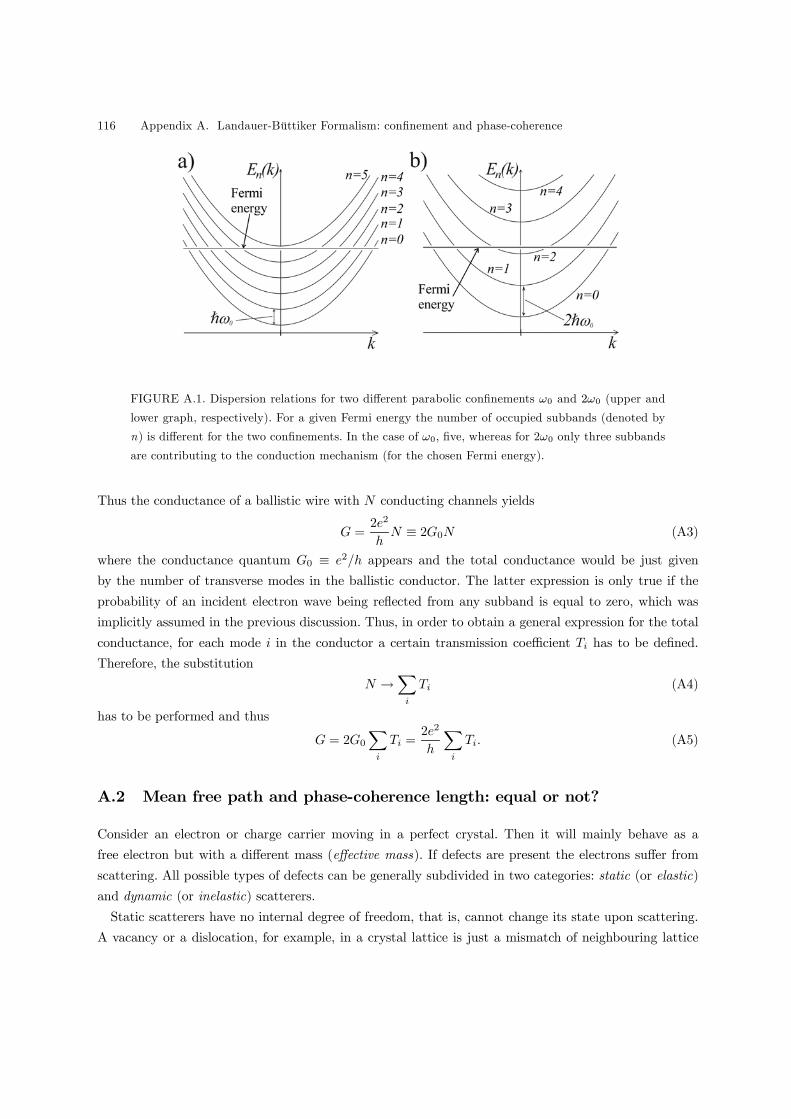
116 Appendix A. Landauer-Büttiker Formalism: confinement and phase-coherence
FIGURE A.1. Dispersion relations for two different parabolic confinements ω0 and 2ω0 (upper and
lower graph, respectively). For a given Fermi energy the number of occupied subbands (denoted by
n) is different for the two confinements. In the case of ω0, five, whereas for 2ω0 only three subbands
are contributing to the conduction mechanism (for the chosen Fermi energy).
Thus the conductance of a ballistic wire with N conducting channels yields
G =2e2
hN ≡ 2G0N (A3)
where the conductance quantum G0 ≡ e2/h appears and the total conductance would be just given
by the number of transverse modes in the ballistic conductor. The latter expression is only true if the
probability of an incident electron wave being reflected from any subband is equal to zero, which was
implicitly assumed in the previous discussion. Thus, in order to obtain a general expression for the total
conductance, for each mode i in the conductor a certain transmission coefficient Ti has to be defined.
Therefore, the substitution
N →Xi
Ti (A4)
has to be performed and thus
G = 2G0Xi
Ti =2e2
h
Xi
Ti. (A5)
A.2 Mean free path and phase-coherence length: equal or not?
Consider an electron or charge carrier moving in a perfect crystal. Then it will mainly behave as a
free electron but with a different mass (effective mass). If defects are present the electrons suffer from
scattering. All possible types of defects can be generally subdivided in two categories: static (or elastic)
and dynamic (or inelastic) scatterers.
Static scatterers have no internal degree of freedom, that is, cannot change its state upon scattering.
A vacancy or a dislocation, for example, in a crystal lattice is just a mismatch of neighbouring lattice

A.2 Mean free path and phase-coherence length: equal or not? 117
FIGURE A.2. A conducting ring to which the voltage V is applied and the current I driven. The ring
diameter is considerably larger than the mean free path lm. The scatterers are static and randomly
distributed along the ring. If a perpendicular magnetic field−→B is applied, the phase-coherence of the
charge carriers moving the upper path and the lower path is preserved as the scatterers are static.
The thin solid black line exemplifies the charge carrier path through the ring.
sites and will remain the same after a collision with a charge carrier. In contrast, dynamic scatterers have
an internal degree of freedom. For example in the case of a lattice vibration (phonon) as a scatterer, a
momentum exchange between electron and phonon is possible. That is, the phonon before and after the
scattering process is not the same. Magnetic impurities are also dynamic scatterers. Upon interacting
with the charge carrier the spin of the impurity might change. Similarly, electron-electron interactions
are also dynamic.
Principally, three possible scattering events are imaginable: (i) the momentum of the electron changes,
(ii) the phase of the electron (wavefunction) changes or (iii) momentum and phase are altered simulta-
neously.
In case (i), the distance that an electron travels before it is changing its momentum due to a collision
is the mean free path lm. Related with lm is the mean free time τm via the expression
lm = υF τm (A7)
where υF is the Fermi-velocity of the electron.
In case (ii), the scattering process is more subtle and for understanding consider the following gedanken-
experiment [63]: a conducting ring connected to two electrode lines as in Fig. A.2 and a voltage applied
across them.
If the ring is without scattering centres, upper and lower path can be regarded as identical, such
that constructive interference due to the definite phase-relationship of each of the charge carriers exist.
Random introduction of static scatterers, lifts the identity of the two paths and the interference may not
be constructive any more. However, since the scatterers are static, a definite phase-relationship between
the two possible paths is still present. That is, the phase-coherence of a charge carrier is preserved [63].
Experimentally this has been confirmed on a metal ring by the application of an external magnetic

118 Appendix A. Landauer-Büttiker Formalism: confinement and phase-coherence
field perpendicular to a ring which size is several hundred times larger than the mean free path [97].
This example shows that the phase-coherence-length lφ can be larger than lm. Similar to lm, the phase-
coherence time is τφ related to lφ.
Now exchange the static by dynamic scatterers as for example by phonons or magnetic impurities. The
phase-relationship between the up- and down-moving electron is no longer defined and varies randomly
with time. An external magnetic field would lead to a variety of constructive and destructive interference
processes which in total would average to zero and therefore in this case one finds lφ ≈ lm. Experimentally,this has been demonstrated in polycrystalline rings in which dynamic impurities have been introduced
via ion implantation [98]. As impurities manganese defects have been chosen [98] as each of them carries
a magnetic moment, i.e., has a spin degree of freedom. The spin degree of freedom can change due to
scattering with conducting electrons which in turn implies that these impurities are dynamic (inelastic)
scatterers.
Finally, consider a defect-free conductor but with non-negligible electron-electron interaction (Coulomb-
interaction). The electrons scatter off each other, yet none of them can be regarded as stationary due
to the mutual Coulomb-interaction. However, the scattering processes do not lead to a net momentum
change, since any momentum loss of one particular electron will be picked up by another one. Thus,
interestingly, the mean free path is not changing but the phase-coherence between the electrons is lost
at any point in time and therefore lφ < lm.
Depending on the system under investigation, therefore, either lφ > lm or lφ ≈ lm or lφ < lm. For the
cases lφ ≈ lm and lφ < lm one finds similar to (A7) the relation
lφ = υF τφ. (A8)

Appendix B
Interaction constants and spin-charge separation inTomonaga-Luttinger liquids
B.1 Interaction constants
In section 3.2.2 and 3.2.3 the Coulomb-interacting electron system of a CNT was described in the frame
of the LL-theory. For this instead of fermionic operators the bosonic phase fields θk and there canonical
momenta Πk, k = c+,c−,s+,s−, were introduced such that the Hamiltonian of the system could be written
in the simple form bH =~υF2
Xk
Z hΠ2k + g
−2k (∂xθk)
2idx. (B1)
The constants gk are the so-called interaction constants for each charge- and spin-mode k and are all
equal to 1 if no interactions are apparent between the fermions. Introducing the Coulomb-interaction
to the system leads to a change of the interaction parameter gc+ which corresponds to the only mode
carrying a charge, therefore gc+ 6= 1. However, although all other modes are in this sense electrically
neutral, their interaction parameters also change as the bosonic fields are by construction to some degree
entangled. In order to see how much these interaction constant deviate from unity it is useful to go a
step back and start with a fermionic description of the interacting electron system in the CNT.
Introducing the 1D fermion (creation) operator ψ(†)pασ(x), where σ denotes for the spin of the elec-
tron, p = ±1 for the two sub-lattices which originate from the two-atomic basis of the graphene-sheet
honeycomb-lattice and the index α = ± for the wavefunction with the Fermi-wavevector ±kF , respec-tively, the free non-interacting Hamiltonian of the electron system can be written as [15]
bH(fermionic)free = −~υF
Xpασ
p
Zψ†pασ(x)∂xψ(−p)ασ(x) dx. (B1)
If a Coulomb-interaction U(−→r ), −→r = (x, y), is acting between the electrons, then in addition tobH(fermionic)free the Hamiltonian
bH(fermionic)C =
1
2
Zρ(x)V (x− x0)ρ(x0) dxdx0
has to be taken into account which ascribes for forward scattering processes and implies the LL-like
behaviour [15]. V (x− x0) is the 1D interaction potential and is given by
V (x− x0) =Z 2πrNT
0
dy
2πrNT
Z 2πrNT
0
U(−→r −−→r 0) dy0
2πrNT(B2)
where rNT is the radius of the CNT and
ρ(x) =Xpασ
ψ†pασ(x)ψpασ(x) (B3)

120 Appendix B. Interaction constants and spin-charge separation in Tomonaga-Luttinger liquids
the 1D electron density [15]. It is noteworthy that bH(fermionic)C is entirely due to the long-ranged tail of
the Coulomb-interaction. For small distances, that is smaller or equal to the average distance aπ of two
π-electron orbitals of neighbouring C-atoms in the honeycomb-lattice, short-ranged interaction processes
start to be of importance [15]. Thus an additional forward scattering and an backscattering contributionbH(fermionic)f and bH(fermionic)
b , respectively, to the total Hamiltonian arise. bH(fermionic)f is of the form
(omitting the arguments of the operators for simplicity)
bH(fermionic)f = −f
Z Xpαα0σσ0
ψ†pασψ†(−p)α0σ0ψ(−p)α0σ0ψpασ dx (B4)
where f ≡ ζfe2aπ/rNT and the parameter ζf is of the order of magnitude 0.05 [15]. Therefore, f << 1.
And bH(fermionic)b can be written as
bH(fermionic)b = b
Z Xpp0ασσ0
ψ†pασψ†p0(−α)σ0ψp0ασ0ψp(−α)σ dx (B5)
where b ≡ ζbe2aπ/rNT ≈ f .
Recall now the bosonized form of the electron system of the CNT, (B1), with the interaction parameters
gk. In section 3.2.2 the interaction parameter of the charge-carrying mode was given as, (3.10),
gc+ ≡ g =·1 +
4
π~υFV (q ≈ 0)
¸−1/2where V (q) is the Fourier transform of the Coulomb-interaction. Naively, the Coulomb-interaction should
not alter the interaction parameters for the electrically neutral modes gk, k 6= c+. However, short-rangeinteractions are also apparent such that the interaction parameters gk, k 6= c+, are renormalized to [15]
gk = 1 +f
π~υF, k 6= c+. (B6)
The term f/ (π~υF ) is due to f << 1 also much smaller than 1, such that in contrast to the Coulomb-interaction, the short-range interactions are for most experimental purposes negligible [15]. However, the
backscattering interaction gives rise to the opening of an energy gap. This energy gap is exponentially
small and can be written in terms of temperature as
Tb =D
kBe−π~ υF√
2b (B7)
where kB is the Boltzmann constant and D ≈ 1 eV (c.f. section 3.1.1) [15]. This corresponds to tempera-tures Tb ≈ 0.1 mK, that is, which is far below the typical temperatures used in most electrical transportmeasurements as it is also the case in the present thesis. Therefore, the interpretation of the experimental
data of with the aid of a LL-like electron-system represented by the CNT is appropriate.
B.2 Spin-charge separation
As indicated by the bosonic description of the interacting electron-system of a CNT, expressed by the
four phase-fields, a decoupling of the charge- and spin-degree of freedom of the electrons in a LL-like state

B.2 Spin-charge separation 121
is present. This is also apparent by the existence of four different interaction parameters as discussed in
the first section of the present Appendix. Only the phase-field θc+ describes electrically charged modes
whereas the other three θcc , θss and θs− are denoting electrically neutral modes [15].
With each of the phase-fields a ”plasmon” velocity [15]
υk =υFgk
(B8)
is connected which in the case of θss and θs− describes the motion of spin through the system. As
gc+ < gs+ , gs− apparently υc+ > υs+, υs− , that is charge- transport is faster in a LL-like CNT than
spin-transport.
Experimentally, the spin-charge separation has not been reported yet. A way of detection, as proposed
by Egger et al. [15] could be a electrical two-terminal measurement on a CNT contacted by two ferro-
magnetic leads with different magnetization directions. Then the current to through system (normalized
to the current with identical magnetizations) is given by [99]
I(φ)
I(0)= 1− P 2 tan2(φ/2)
tan2(φ/2) + Y(B9)
where φ is the angle between the two magnetizations, P the polarization of the ferromagnetic leads
according to the difference in the density of states for up and down spin and Y accounts for spin-mixing
effects.
For non-LL-like samples contacted Y is a constant, but for a LL-like CNT Y and also I(0) will
depend on the applied source-drain voltage Vsd such that (B9) has to be modified. I(0) has in this
case to be renormalized by the power-law suppression factor V γ/2sd and Y will be diverging towards zero
temperature T and zero Vsd according to [max(eVsd, kBT )]−γ [15]. Although this experiment seems rather
straightforward, a severe bottleneck is found in the exact tunability of the directions of the magnetizations
on a nanoscopic scale and the high accuracy required to detect the effect, as implied by (B9).
However, experiments similar to the one described here has been performed on SWNTs and MWNTs
[58], but the work focused more on the spin-valve-effect than on LL properties of the CNTs which for
MWNTs are itself questionable as discussed in section 3.2.4.

122 Appendix B. Interaction constants and spin-charge separation in Tomonaga-Luttinger liquids

Appendix C
Constant interaction model
In section 6.1 and 6.2 single-electron effects of a electrically weakly coupled island, either FL-like or LL-
like has been discussed. The energy difference between two groundstates with n+ 1 and n electrons on
the island was given by µ(n+1; Vl) = E(n+1, 0; Vl)−E(n, 0; Vl) (see (6.1)). Thus, if, for example,tunneling through the island containing n electrons in the groundstate, the energy required µ(n+1; Vl).The last expression is of general validity and not restricted to any special electrical properties of the island
itself, yet.
The constant interaction model (CIM) [68] is the simplest model that can be applied in order to
describe the properties of the island. This heuristic model assumes that the interactions between the
particles do no depend on the number of electrons n on the island. This conditions are usually fulfilled
for FL-like, metallic islands.
Recalling that an electron −e added to the island influences image charges δe(i) on the surroundingelectrodes, between each of the electrodes and the island a constant capacitance Ci can be defined.
Therefore the island can be electrically described by a single constant capacitance
C =Xi
Ci. (C1)
The potential of the island Visland can then be found by noting that it can be expressed by the potentials
Vl of the surrounding electrodes and the total additional charge q on the island Visland = q/C+Pl αlVl,
where the αl’s are the capacitive coupling constants between each electrode and the island. The energy
required for charging the island with −ne is therefore given by
E(n+ 1) =
Z −ne0
Visland(q) dq =(ne)2
2C− ne
Xl
αlVl. (C2)
Therefore µCIM(n+ 1; Vl) ≡ E(n+ 1)−E(n) = (n+ 12)e
2/C − ePl αlVl (analogous to the general
case) and finally one finds the energy difference
µCIM(n+ 1; Vl)− µCIM(n; Vl) =e2
C(C3)
where e2/2C is also called the Coulomb energy Ec. Obviously, in the CIM Ec does not depend on the
number of charges n on the island, such that the transport regions for groundstate transitions in the
(Vsd vs. Vg)-plane are all equally in size. In section 6.1 and 6.2, this has been assumed for simplicity to
keep the (Vsd vs. Vg)-plane more comprehensible and not to divert from the main effects caused by the
tunneling density of states τ(ε) ∼ εγ of the LL-like island.
As the CIM is based on the assumption of an invariant interaction strength between the electrons
on the island with respect to the number n, it is evident that this simple model cannot be applied to
LL-like islands. These have heavily interacting electron-systems and are extremely sensitive to external

124 Appendix C. Constant interaction model
perturbations. This sensitivity leads to the circumstance that LL-like islands exhibit only collective
excitations [38]. Therefore in order to describe and interpret the electrical transport of electrically weakly
coupled SWNTs a more general description, as it was done in chapter 6, than the CIM has to be
considered.

Appendix D
More grey-scale plots
In section 6.3 I/Vsd- characteristics for different Vg have been presented as grey-scale plots. In Fig. D.1
the corresponding grey-scale plot to the electrode pair (I) with a step-size Vg for of 200 mV. The two
parallel white dotted lines close to zero Vsd correspond to the theoretically predicted width of 4∆0/e ≈3.6 mV for the currentless band. Only very shallow irregular diamond-like structures are visible (white
dotted as guide for the eye). No significant dark or white spots are apparent indicative for QP tunneling
induced current peaks.
FIGURE D.1. Grey-scale plot of the I/V sd -characteristics for different V g for electrode pair (I) in Fig.
6.11. V g was changed in steps of 200 mV. Dark denotes increasing negative, bright increasing positive
current (depending on V sd ). A currentless band of somewhat larger width than the theoretically
predicted width (indicated by the two parallel dashed lines) of 4∆0/e ≈ 3.6 mV is observed. Some
diamond-like features are visible in outlines (see dotted lines). For better contrast, the ”height-lines”
of the current are also plotted (dashed, dark grey)
The situation depicted in Fig. D.2 is similar to the one in Fig. D.1: a currentless band around zero Vsdis visible of about 4 mV width. Again no pronounced current peaks are visible. The rhomb-like features
are not well developed and seem to be of irregular shape.

126 Appendix D. More grey-scale plots
FIGURE D.2. Grey-scale plot of the I/V sd -characteristics for different V g of electrode pair (II) in Fig.
6.11. The stepsize for V g was 200 mV. Again a currentless band of similar width as the theoretically
predicted width of about 3.6 mV (two parallel dashed lines) is visible. diamond-like structures are
only weakly pronounced and some are indicated by dotted lines. Dark denotes increasing negative,
bright increasing positive current. For better contrast, the current ”height-lines” are also depicted
(dashed, dark grey).
Thus, the experimental data shown here for the electrode pairs (I) and (II), apparently, are similar
to those of the presented samples in section 6.3. In all of them a currentless band is observed and the
irregularity of the diamond-like structure is also confirmed as predicted by the proposed model in sections
6.1 and 6.2. However, no prominent dark or white spots are apparent indicating a suppression of QP
tunneling induced current peaks.

Appendix E
Perturbation approach to the electrical MagnetochiralAnisotropy
E.1 Ballistic charge transport
In the case of a ballistic conductor, the charge carriers can be regarded to traverse the object without
suffering from any scattering process. If the conductor is chiral, then R = R³−→B,−→j´. Time-reversal
symmetry and invariance of scalar quantities under bT requirebTR³−→B,−→j ´ = R³−−→B,−−→j ´ = R³−→B,−→j ´ (E1)
and thus leading to
R³−→B,−→j´
= R0 + α1−→B 2 + β1
−→j 2 + γ11
−→j 2 ·−→B 2 + χ
D/L00
−→j ·−→B (E2)
+o³−→j 2p+1 ·−→B 2q+1
´+ o
³−→j 2k ·−→B 2r
´with appropriate coefficients in each of the sums. In order to get the allowed dependences of the resistance,
the parity operation has yet to be applied, yielding
bPR³−→B,−→j ´ = R0 + α1−→B 2 + β1
³−−→j
´2+ γ11
³−−→j
´2·−→B 2 + χ
D/L00
³−−→j
´·−→B (E3)
+o
µ³−−→j
´2p+1·−→B 2q+1
¶+ o
µ³−−→j
´2k·−→B 2r
¶= R
³−→B,−→j´.
The terms χD/L00
³−−→j
´· −→B and o
µ³−−→j
´2p+1·−→B 2q+1
¶in (E3) seem to be contradictory with the
requirement of invariance R³−→B,−→j´under bP . But bP has also to be applied to the coefficients in (E3). As
the conductor is chiral the coefficients of the terms of odd power in−→B and
−→j change sign under bP , such
that no contradiction is apparent any more. To the lowest order, the symmetry allowed dependences of
the resistance for a chiral ballistic conductor are then given by the expression
R³−→B,−→j´≈ R0 + α1
−→B 2 + χ
D/L00
−→j ·−→B + o
³−→j 2p+1 ·−→B 2q+1
´(E4)
where the terms
χD/L00
−→j ·−→B + o
³−→j 2p+1 ·−→B 2q+1
´(E5)
denote the so-called eMChA.

128 Appendix E. Perturbation approach to the electrical Magnetochiral Anisotropy
E.2 Diffusive charge transport
For diffusive electrical transport one has to use the Onsager relation [88] for the electrical conductivity.
Assume σik = σik
³−→B´. Then applying Onsager’s relation leads to
σik³−→B´= σki
³−−→B
´. (E6)
As σik is a component of a tensor, it can be written as the sum of a symmetric part sik and an
asymmetric part aik. Therefore it follows
σik
³−→B´= sik
³−→B´+ aik
³−→B´. (E7)
According to Onsager’s relation one is led to the expression
σik
³−→B´
= sik
³−→B´+ aik
³−→B´
(E8)
= ski³−−→B
´+ aki
³−−→B
´= σki
³−−→B
´.
As sik³−→B´is symmetric, that is sik
³−→B´= ski
³−→B´∀i, k, applying Onsager’s relation one finds
sik
³−→B´= sik
³−−→B
´. Consequently, sik
³−→B´only terms with
−→Bn are allowed where n is an even integer.
aik
³−→B´is an asymmetric quantity, that is aik
³−→B´= −aki
³−→B´∀i, k which implies that aii
³−→B´= 0.
Applying Onsager’s relation here yields aik³−→B´= −aik
³−−→B
´. Therefore, aik
³−→B´can only depend
on−→Bm where m is an odd integer. In order to extract the allowed
−→B -dependences, the parity-reversal
operation as yet to be performed
bPσik ³−→B´ = σik
³ bP−→B´ = σik
³−→B´. (E9)
Then for the symmetric sik³−→B´and the asymmetric part aik
³−→B´it follows, that both are unaltered
by the the parity-reversal operation and σik³−→B´contains even as well as odd powers in
−→B . But the
diagonal elements σii³−→B´, which describe the longitudinal conductivity, are only determined by the
symmetric part of the conductivity tensor.
In the case of a diffusive chiral conductor, the conductivity tensor σ depends on the current density−→j and the magnetic field
−→B . Writing σ in terms of components yields
σik³−→j ,−→B´= sik
³−→j ,−→B´+ aik
³−→j ,−→B´. (E10)
Then the Onsager relation requires sik³−→j ,−→B´= ski
³−−→j ,−−→B
´and aik
³−→j ,−→B´= aki
³−−→j ,−−→B
´and the corresponding symmetries of sik
³−→j ,−→B´and aik
³−→j ,−→B´lead to
sik³−→j ,−→B´
= sik³−−→j ,−−→B
´(E11)
aik
³−→j ,−→B´
= −aik³−−→j ,−−→B
´.
E.2 Diffusive charge transport 129
The asymmetric part aik³−→j ,−→B´, therefore, has to be of the form
aik
³−→j ,−→B´
= a(0)ik + ²
(0)ik
¯−→B¯+ ε
(0)ik
¯−→j¯
(E12)
+o³−→j 2k ·−→B 2r+1
´+ o
³−→j 2p+1 ·−→B 2q
´and the symmetric part sik
³−→j ,−→B´yields
sik³−→j ,−→B´
= s(0)ik + α
(1)ik
−→B 2 + β
(1)ik
−→j 2 + κD/Lik,00
−→j ·−→B (E13)
+o³−→j 2p+1 ·−→B 2q+1
´+ o
³−→j 2k ·−→B 2r
´.
As the parity operation requires bPσik ³−→j ,−→B´ = σik
³ bP−→j , bP−→B´ = σik
³−−→j ,−→B
´= σik
³−→j ,−→B´the
allowed dependences of the asymmetric part of the conductivity tensor in−→B and
−→j reduces to (omitting
higher order terms)
aik³−→j ,−→B´= a
(0)ik + ²
(0)ik
¯−→B¯+ ζ
(10)ik
−→j 2 ·
¯−→B¯. (E14)
The symmetric part remains unaltered by bP except for the terms of odd power in−→B and
−→j . But the
conductor is chiral and therefore these terms are conserved as the corresponding coefficients change sign
under bP : exemplified for the linear part asbPκDik,00 = κLik,00 with κDik,00 = −κLik,00. (E15)
The symmetric part thus can be written as (omitting higher order terms)
sik
³−→j ,−→B´≈ s(0)ik + α
(1)ik
−→B 2 + κD/Lik,00
−→j ·−→B + o
³−→j 2p+1 ·−→B 2q+1
´. (E16)
discovering the eMChA again.

130 Appendix E. Perturbation approach to the electrical Magnetochiral Anisotropy

Appendix F
Details on the ballistic free electron on a helix model
In the ballistic case the electron on the helix is described by the trial 3D wave-function
eΨn (ρ,ϕ, z) = Cn exp−µρ− ad
¶2exp−
³ad
³ϕ− z
b
´´2(F1)
× expµinϕ
N
¶exp
µinz
bN
¶≡ Rn(ρ)Fn(z,ϕ)
For the three-dimensional wavefunctions in the contacts in the symmetrical gauge
Φ−→Rl,µ,kz (
−→r ) = Φl,µ,kz³−→r −−→R´ expà i−→r ×−→R
2`2
!(F2)
is used [100] where−→R denotes the position of the center-of-mass of the cyclotron orbit and
Φl,µ,kz (ρ,ϕ, z) =Cl,µ√L
µρ√2`
¶|µ|L|µ|l+|µ|
µρ2
2`2
¶(F3)
× expµ− ρ2
4`2+ ikzz + iµϕ
¶≡ Rl,µ(ρ) exp (iµϕ) exp (ikzz) .
The quantum number l is a positive integer or zero, µ is an integer,√2` the cyclotron radius and Lnm is
an associated Laguerre polynomial, with
Cl,µ =
√l!
` ((l + |µ|)!)3/2(F4)
The energy of the contact states are therefore given by [101]
El,µ,kz =~qm
µl |B|+ µB + |µ| |B|+ |B|
2
¶+~2k2z2m
(F5)
with an angular momentum
LzΦl,µ,kz = µ~Φl,µ,kz . (F6)
For the following considerations, it is assumed that the effective mass of the electron is the same in
the contact and on the helix. Then the transmission coefficients Tc→h and Th→c are determined by the
condition that the incident and reflected wavefunctions are matched to the transmitted wavefunctions
at the helix-contact junction (z = 0) [102],[103]. Further the considerations are limited to the case of
low temperatures and contact states centered on the helix position, that is,−→R = 0 . This approach
represents already an approximation, as charge accumulation effects in the vicinity of the junction have
been neglected.
132 Appendix F. Details on the ballistic free electron on a helix model
F.1 Transmission from helix to contact
The boundary conditions for incident and reflected wavefunctions yield
Rn(ρ)Fn(0,ϕ) + rnRn(ρ)Fn(0,ϕ) =Xl,µν
tn,l,µνRl,µν (ρ) exp (iµνϕ) (F7)
and
iknRn(ρ)Fn(0,ϕ) + 2a2
d2ϕ
bRn(ρ)Fn(0,ϕ) (F8)
−iknrnRn(ρ)Fn(0,ϕ)− 2a2
d2ϕ
brnRn(ρ)Fn(0,ϕ)
=Xl,µν
tn,l,µν (ikzν )Rl,µν (ρ) exp (iµνϕ)
with kn ≡ nbN and rn the reflection- and tn,l,µν transmission-probability of the incident wavefunctioneΨn (ρ,ϕ, z).
Multiplying (F7) with Rl0,µν0 (ρ) exp (−iµν0ϕ), integrating over ρ and ϕ, and use of orthonormality
yields
Rn,l0,µν0Ωn,µν0
®+ rnRn,l0,µν0Ωn,µν0 =
Xl,µν
tn,l,µνδl,l0δν,ν0 . (F9)
Therefore one obtains
rn = tn,l0,µν01
Rn,l0,µν0Ωn,µν0− 1 (F10)
where
Rn,l0,µν0 ≡Rn(ρ)|Rl0,µν0 (ρ)
®(F11)
and
Ωn,µν0 ≡ hFn(0,ϕ) | exp (−iµν0ϕ)i (F12)
are the expectation values for the radial and the angular part of the wave-functions, respectively.
Similarly for (F8) it follows
ikn(1− rn)Rn,l0,µν0Ωn,µν0 + 2a2
d21
b(1− rn)Rn,l0,µν0Ωn,µν0ϕ = tn,l0,µν0 ikzν0 (F13)
with
Ωn,µν0 (ϕ) ≡ hFn(0,ϕ) | ϕ | exp (−iµν0ϕ)i (F14)
The expectation values Ωn,µν0 and Ωn,µν0 (ϕ) can be determined as

F.1 Transmission from helix to contact 133
Ωn,µν0 =
2πZ0
exp−·³adϕ´2+ i³µν0 −
n
N
´ϕ
¸dϕ (F15)
= exp−µd
2a
³µν0 −
n
N
´¶2 2πZ0
exp−µa
dϕ+ i
d
2a
³µν0 −
n
N
´¶2dϕ
=d
aexp−
µd
2a
³µν0 −
n
N
´¶2 2π adϕ+i
d2a(µν0− n
N )Zi d2a (µν0− n
N )
exp−u2du
=
√πd
2aexp−
µd
2a
³µν0 −
n
N
´¶2×·erf
µ2πa
dϕ+ i
d
2a
³µν0 −
n
N
´¶− erf
µid
2a
³µν0 −
n
N
´¶¸≈√πd
2aexp−
µd
2a
³µν0 −
n
N
´¶2where for the last step d << a and the strong rising properties in the argument of the error-function
erf(x) has been used.
In analogy one finds
Ωn,µν0 (ϕ) = i∂
∂µν0Ωn,µν0 (F16)
≈ i∂
∂µν0
√πd
2aexp
Ã−µd
2a
³µν0 −
n
N
´¶2!
= −i2√πµd
2a
¶3 ³µν0 −
n
N
´exp
Ã−µd
2a
³µν0 −
n
N
´¶2!.
The ratio of the two expectation values is therefore given by
Ωn,µν0 (ϕ)
Ωn,µν0≈ −i
2√π¡d2a
¢3 ¡µν0 − n
N
¢exp
³− ¡ d2a ¡µν0 − n
N
¢¢2´√πd2a exp
³− ¡ d2a ¡µν0 − n
N
¢¢2´ (F17)
= −i2µd
2a
¶2 ³µν0 −
n
N
´.
Combining (F10), (F13) and utilizing (F17) leads to the transmission probability for eΨn (ρ,ϕ, z)tn,l0,µν0 = 2Rn,l0,µν0Ωn,µν0
kn − 1b
¡µν0 − n
N
¢kzν0 + kn +
1b
¡µν0 − n
N
¢ . (F18)

134 Appendix F. Details on the ballistic free electron on a helix model
As the current transmission coefficient Th→c from the helix into the contact is given by the summation
over all states (wavefunction) involved in the current transport one finds
Th−→c =X
EF=El,µ,kzν
¯¯2 Rn,l,µν® Fn,µν® kn − 1
b
¡µν0 − n
N
¢kzν0 + kn +
1b
¡µν0 − n
N
¢ ¯¯2
(F19)
where the accents have been dropped for simplicity and use of the circumstance has been made, that at
low temperatures mainly states at the Fermi energy EF are contributing to the current transport.
The sum can be reduced by utilizing n = nF and that Rn,l,µ and Ωn,µν0 are strongly peaked for l = 0,
and eµ = nFN , respectively,
Th−→c ≈ 4¯RnF ,0,nFN
ΩnF ,nFN
¯2Ã knFekz + knF!2. (F20)
From energy conservation the wavevector component ekz in the contact is deduced to beekz ≡ ±
r2m
~2
µEF − ~q
m
µB + |µ| |B|+ |B|2
¶1/2(F21)
≈ kF
µ1 +
~q2mEF
eµB + |eµ| |B|+ |B|2
¶= kF
µ1 +
~q4mEF
nFB + |nF | |B|+N |B|N
¶with kF ≡ ±
q2mEF~2 being the contact Fermi wavevector at zero magnetic field.
F.2 Transmission from contact to helix
Consider a state (l, µ, kz) in the contact incident on the helix at z = 0. Using the same boundary
conditions as in the case for Th→c one obtains
Rl,µ(ρ) exp (iµϕ) +X
l0,µ0,k0z
rl0,µ0,k0zl,µ,kz
Rl0,µ0(ρ) exp (iµ0ϕ) = tn,l,µRn(ρ)Fn(0,ϕ) (F22)
and
ikzRl,µ(ρ) exp (iµϕ) (E23)
+X
l0,µ0,k0z
rl0,µ0,k0zl,µ,kz
(−ik0z)Rl0,µ0(ρ) exp (iµ0ϕ)
= tn,l,µ
µikn + 2
a2
d2ϕ
b
¶Rn(ρ)Fn(0,ϕ)
Multiplying with Rn(ρ)F ∗n(0,ϕ), integrating over ρ and ϕ, using the orthonormality properties of the
wavefunctions yields
Rn,l,µΩ∗n,µ +
Xl0,µ0,k0z
rl0,µ0,k0zl,µ,kz
Rn,l0,µ0Ω∗n,µ0 = tn,l,µ (F24)

F.2 Transmission from contact to helix 135
and
ikzRn,l,µΩ∗n,µ −
Xl0,µ0,k0z
rl0,µ0,k0zl,µ,kz
(ik0z)Rn,l0,µ0Ω∗n,µ0 =
½ikn + 2
a2
d21
bhϕi¾
(F25)
where rl0,µ0,k0zl,µ,kz
and tn,l,µ are the corresponding reflection and transmission coefficients of the incident
contact wavefunction Φl,µ,kz (ρ,ϕ, z). The expectation value hϕi is given by
hϕi ≡ hFn(0,ϕ) | ϕ | Fn(0,ϕ)i . (F26)
Conservation of angular momentum conservation leads to rl0,µ0,k0zl,µ,kz
= rl0,µ0,k0zl,µ,kz
δµ,µ0 and therefore rl0,µ0,k0zl,µ,kz
=
rl0,k0zl,µ,kz
. Additionally, due to the considerable difference in the spatial extension of the wavefunction in the
contact and the helix wavefunction it follows rl0,k0zl,µ,kz
δl,l0 = rk0zl,µ,kz
. Finally, energy conservation requires
|kz| = |k0z|. Therefore the sum in the latter two equations can be reduced to
Rn,l,µΩ∗n,µ + rl,µ,kzRn,l,µΩ
∗n,µ = tn,l,µ (F27)
and
ikzRn,l,µΩ∗n,µ − rl,µ,kz ikzRn,l,µΩ∗n,µ = tn,l,µ
½ikn + 2
a2
d21
bhϕi¾
(F28)
Evaluating hϕi,
hϕi =
2πZ0
ϕ exp−³√2a
dϕ´2dϕ (F29)
= − 1
2¡√2ad¢2 ·exp−8π2 ³ad´2 − 1
¸
=
µd
2a
¶2 ·1− exp−8π2
³ad
´2¸≈
µd
2a
¶2and noting that Rn,l,µ is strongly peaked for l = 0 for all n, µ one finally obtains
Rn,0,µΩ∗n,µ + rl,µ,kzRn,0,µΩ
∗n,µ = tn,l,µ (F30)
and
ikzRn,0,µΩ∗n,µ − rl,µ,kz ikzRn,0,µΩ∗n,µ ≈ tn,l,µ
½ikn +
1
2b
¾. (F31)
The combination of the last two equations yields for the transmission coefficient of the incident contact
wave
tn,l,µ = Rn,0,µΩ∗n,µ
i2kz£i (kn + kz) +
12b
¤ . (F32)

136 Appendix F. Details on the ballistic free electron on a helix model
Since Tc−→h =PEF=El,µ,kz
|tn,l,µ|2 , use of n = nF ,and that Ωn,µν0 is strongly peaked at eµ = nF/N ,the current transmission coefficient from contact into helix is found to be
Tc−→h ≈¯DRnF ,0,
nFN
EDFnF ,
nFN
E¯2 4 ekz2³ ekz + kn´2 + 14b2
. (F33)
The total current transmission coefficient T is therefore
T = Th−→cTc−→h (F34)
≈ 4¯RnF ,0,
nFNΩnF ,
nFN
¯2Ã knFekz + knF!2
ׯRnF ,0,
nFNΩnF ,
nFN
¯2 4 ekz2³ ekz + kn´2 + 14b2
= 16¯RnF ,0,nFN
ΩnF ,nFN
¯4 ekz2k2nF³ ekz + knF´4 + 14b2
³ ekz + knF´2Assuming for b typical values that can be found for CNTs (b . 1 nm) and the wavevectors knF , ekz to
be of the order of magnitude of a few Å−1, T can be expressed as
T ≈ 16¯DRnF ,0,nFN
EDFnF ,nFN
E¯4 ekz2k2nF³ ekz + knF´4 . (F35)

References[1] S. Iijima, Nature 354, p. 56 (1991).
[2] picture taken from homepage of R.E. Smalley at Rice University, USA:
http://cnst.rice.edu/smalleygroup/res.htm.
[3] M. Bockrath, D.H. Cobden, P.L. McEuen, N.G. Chopra, A. Zettl, A. Thess and R.E. Smalley,
Science 275, p.1922 (1997).
[4] S.J. Tans, M.H. Devoret, H. Dai, A. Thess, R.E. Smalley, L.J. Geerligs and C. Dekker, Nature 386,
p. 474 (1997).
[5] A. Bachtold, M.S. Fuhrer, S. Plyasunov, M. Forero, E.H. Anderson, A. Zettl and P.L. McEuen,
Phys. Rev. Lett. 84, p. 6082 (2000).
[6] M. Bockrath, D.H. Cobden, J. Lu, A.G. Rinzler, R.E. Smalley, L. Balents and P.L. McEuen, Nature
397, p. 598 (1999).
[7] A. Bachthold, C. Strunk, J.-P. Salvetat, J.-M. Bonard, L. Forro, T. Nussbaumer and C. Schönen-
berger, Nature 397, p. 673 (1999).
[8] G.L.J.A. Rikken and E. Raupach, Nature 390, p. 493 (1997).
[9] G.L.J.A. Rikken and E. Raupach, Phys. Rev. E 58, p. 5081 (1998).
[10] G.L.J.A. Rikken, J. Fölling and P. Wyder, Phys. Rev. Let. 87, p. 236602 (2001).
[11] J.W. Mintmire and C.T. White in Carbon Nanotubes - Preparation and Properties, ed. by T.W.
Ebbesen, CRC Press (Boca Raton, 1997), p. 191-209.
[12] Gmelins Handbuch der anorganischen Chemie 14, 8th edition, Teil B - Lieferung 2, Verlag Chemie
GmbH (Weinheim, 1968), p. 651-652.
[13] For an overview see J. Israelachvili, Intermolecular & Surface Forces, 2nd edition, Academic Press
(London, San Diego, 1992).
[14] R. Saito, G. Dresselhaus, M.S. Dresselhaus, Physical Properties of Carbon Nanotubes, Imperial
College Press (London, 1998), p. 17-33.
[15] R. Egger, A. Bachtold, M.S. Fuhrer, M. Bockrath, D.H. Cobden and P.L. McEuen in Interact-
ing electrons in Nanostructures, ed. by R. Haug and H. Schoeller, Lecture Notes in Physics 579,
Springer-Verlag (Berlin, Heidelberg, New York, 2001), p. 125-146.
138 References
[16] R. Saito, G. Dresselhaus and M.S. Dresselhaus, Physical Properties of Carbon Nanotubes, Imperial
College Press (London, 1998), p. 68.
[17] J.W.G. Wildöer, L.C. Venema, A.G. Rinzler, R.E. Smalley and C. Dekker, Nature 391, 59 (1998).
[18] N.D. Lang in Scanning Tunneling Microscopy III, ed. by R. Wiesendanger and H.-J. Güntherodt,
Springer Series in Surface Sciences 29, Springer Verlag (Berlin, Heidelberg, New York, 1993), p.
7-21.
[19] For an overview on this topic see H. Böttger and V.V. Bryskin, Hopping Conduction in Solids,
VCH (Weinheim, 1985).
[20] J. Muster, G.T. Kim, V. Krstic, J.G. Park, Y.W. Park, S. Roth and M. Burghard, Adv. Mater.
12, p. 420 (2000).
[21] J. Kondo, Prog. Theor. Phys. 32, p. 37 (1964).
[22] R. de Picciotto, H.L. Stormer, L.N. Pfeiffer, K.W. Baldwin and K.W. West, Nature 411, p. 51
(2001).
[23] S. Datta, Electronic Transport in Mesoscopic Systems, Cambridge University Press (1995), p. 53-54.
[24] For an review on this topic see S. Datta, Electronic Transport in Mesoscopic Systems, Cambridge
University Press (1995), and Y. Imry, Introduction to Mesoscopic Physics, Oxford University Press,
Inc. (1997).
[25] B.J. van Wees et al., Phys. Rev. Lett. 60, p. 848 (1988). D. Wharam et al., J. Phys. C 21, p. L209
(1988).
[26] R. Saito, G. Dresselhaus and M.S. Dresselhaus, Physical Properties of Carbon Nanotubes, Imperial
College Press (London, 1998), p. 137-159.
[27] C.T. White and T.N. Todorov, Nature 393, p. 240 (1998).
[28] S. Frank, P. Poncharal, Z.L. Wang and W.A. de Heer, Science 280, p. 1744 (1998).
[29] S. Sanvito, Y.K. Kwon, D. Tomanek, C.J. Lambert, Phys. Rev. Lett. 84, p.1974 (2000).
[30] M.S. Fuhrer, M. Forero, A. Zettl, P.L. McEuen in Electronic Properties of Molecular Materials ed.
by H. Kuzmany, J. Fink, M. Mehring, S. Roth, AIP 591, New York, p. 401-404 (2001).
[31] J. Hone, B. Batlogg, Z. Benes, A.T. Johnson and J.E. Fisher, Science 289, p.1730 (2000).
[32] Z. Yao, C.L. Kane and C. Dekker, Phys. Rev. Lett. 84, p. 2941 (2000).
[33] For an overview see J.M. Ziman, Electrons and Phonons, Oxford University Press (Oxford, 1979).
[34] T. Hertel and G. Moos, Phys. Rev. Lett. 84, p. 5002 (2000).

References 139
[35] G. Grüner, Density Waves in Solids, Frontiers in Physics 89, Addison-Wesley Publishing Company
(Massachusetts, Menlo Park, Ney York, 1994), p.1-8.
[36] C.L. Kane and M.P.A. Fisher, Phys. Rev. B 68, p. 15233 (1992).
[37] F.D.M. Haldane, Phys. Rev. Lett. 47, p. 1840 (1981).
[38] C.L. Kane and M.P.A. Fisher, Phys. Rev. Lett. 68, p. 1220 (1992).
[39] C. Schönenberger, A. Bachthold, C. Strunk, J.P. Salvetat, L. Forro, Appl. Phys. A 69, p. 283
(1999).
[40] L. Langer, V. Bayot, E. Grivei, J.P. Issi, J.P. Heremans, C.H. Olk, L. Stockman, C. VanHaesendonck
and Y. Bruynseraede, Phys. Rev. Lett. 76, p. 479 (1996).
[41] E.G. Mishchenko, A.V. Andreev and L.I. Glazman, Phys. Rev. Lett. 87, p. 2468011 (2001).
[42] S. Roche, F. Triozon, A. Rubio and D. Mayou, Phys. Lett. A 285, p. 94 (2001).
[43] C. Journet, W.K. Maser, P. Bernier, A. Loiseau, M. Lamy de la Chapelle, S. Lefrant, P. Deniard,
R. Lee and J.E. Fisher, Nature 388, p. 756 (1997). S. Iijima, Nature 354, p. 56 (1991).
[44] A. Thess, R. Lee, P. Nikolaev, H. Dai, P. Petit, J. Robert, C. Xu, Y.H. Lee, S.G. Kim, A.G.
Rinzler, D.T. Colbert, G.E. Scuseria, D. Tomanek, J.E. Fischer and R.E. Smalley, Science 273, p.
483 (1996).
[45] J. Kong, C. Zhou, A. Morpurgo, H.T. Soh, C.F. Quate, C. Marcus and H. Dai, Appl. Phys. A 69,
p. 305 (1999).
[46] M.J. Bronikowski, P.A. Willis, D.T. Colbert, K.A. Smith and R.E. Smalley, J. Vac. Sci. & Tech. A
19, p.1800 (2001).
[47] G.S. Duesberg, J. Muster, V. Krstic, M. Burghard and S. Roth, Appl. Phys. A-Mater. Sci. &
Process. 67, p. 117 (1998).
[48] V. Krstic, G.S. Düsberg, J. Muster, M. Burghard and S. Roth, Chem. Mater. 10, p. 2338 (1998).
[49] A. Bachtold, M. Henny, C. Tarrier, C. Strunk, C. Schonenberger, J.-P. Salvetat, J.-M. Bonard and
L. Forro, Appl. Phys. Lett. 73, p. 274 (1998).
[50] V.V. Schmidt The Physics of Superconductors, edited by P. Müller and A.V. Ustinov, Springer-
Verlag (Berlin, Heidelberg, New York, 1997), pp. 54.
[51] A.Y. Kasumov, R. Deblock, M. Kociak, B. Reulet, H. Bouchiat, I.I. Khodos, Y.B. Gorbatov, V.T.
Volkov, C. Journet and M. Burghard, Science 284, p. 1508 (1999).
[52] A.F. Morpurgo, J. Kong, C.M. Marcus and H. Dai, Science 286, p .263 (1999).

140 References
[53] V.V. Schmidt The Physics of Superconductors, edited by P. Müller and A.V. Ustinov, Springer-
Verlag (Berlin, Heidelberg, New York, 1997), p. 2.
[54] Gmelins Handbuch der anorganischen Chemie 37, 8th edition, Verlag Chemie GmbH (Weinheim,
1969), p. 24 and p. 46.
[55] private communication with M.R. Buitelaar, Universität Basel, Switzerland.
[56] C.P. Colliere, E.W. Wong, M. Belohradský, F.M. Raymo, J.F. Stoddart, P.J. Kuekes, R.S. Williams
and J.R. Heath, Science 285, p. 391 (1999).
[57] Supraleitende Werkstoffe, ed. by O. Henkel and E.M. Sawitzkij, VEB, (Leipzig, 1982), pp. 240.
[58] K. Tsukagoshi, B.W. Alphenaar and H. Ago, Nature 401, p. 572 (1999). K. Tsukagoshi and B.W.
Alphenaar, Superlatt. Microstruc. 27, p. 565 (2000).
[59] H. Sellers, Surf. Sci. 294, p. 99 (1993). E. Sabatini, J. Cohenboulakai, M. Bruening and I. Rubin-
stein, Langmuir 9, p. 2974 (1993).
[60] M. Büttiker, Phys. Rev. Lett. 57, p. 1761 (1986).
[61] M. Büttiker, IBM J. R. Develop 32, p. 317 (1988).
[62] M. Büttiker, Phys. Rev. B 33, p. 3020 (1986).
[63] S. Datta, Electronic Transport in Mesoscopic Systems, Cambridge University Press (1995), p. 99-
102.
[64] J. Nygård, D.H. Cobden, M. Bockrath, P.L. McEuen, and P.E. Lindelof, Appl. Phys. A: Mater Sci.
Process. 69, 297 (1999).
[65] A. Bezryadin, A.R.M. Verschueren, S.J. Tans and C. Dekker, Phys. Rev. Lett. 80, p. 4036 (1998).
[66] A. Bachtold, C. Strunk, C. Schönenberger, J.-P. Salvetat and L. Forro, in Electronic Properties of
Novel Materials: Progress in Molecular Nanostructures, XII International Winterschool, Kirchberg,
Austria 1998, ed. by H. Kuzmany, J. Fink, M. Mehring and S. Roth, AIP Conference Proceedings
No. 442 (Woodbury, New York, 1998), p. 65-68.
[67] H.R. Shea, R. Martel and P. Avouris, Phys. Rev. Lett. 84, p. 4441 (2000).
[68] L.I. Glazman in Single electron tunneling, J. Low Temp. Phys. 118, p. 247-269 (2000). A.N. Ko-
rotkov in Molecular Electronics, Blackwell (Oxford, UK, 1977) pp.178.
[69] J. Weis, R.J. Haug, K. v. Klitzing, K. Ploog, Semicond. Sci. Technol. 9, p. 1890 (1994).
[70] V. Krstic, J. Muster, G.S. Düsberg, G. Philipp, M. Burghard and S. Roth, Synth. Met. 110, p.
245 (2000).
References 141
[71] A. Rochefort, P. Avouris, F. Lesage and D.R. Salahub, Phys. Rev. B 60, p. 13824 (1999).
[72] M.C. Petty and W.A. Barlow in Langmuir-Blodgett Films, Plenum (New York, 1990), p. 115-118.
[73] V.V. Schmidt The Physics of Superconductors, edited by P. Müller and A.V. Ustinov, Springer-
Verlag (Berlin, Heidelberg, New York, 1997), p. 139-164.
[74] D.C. Ralph, C.T. Black and M. Tinkham, Phys. Rev. Lett. 74, p. 3241 (1995).
[75] D. Pfannkuche, S. E. Ulloa, Advances in Solid State Physics 35, ed. by R. Helbig, Vieweg, 65
(1996). D. Weinmann, W. Häusler, B. Kramer, Annal. d. Phys. 5, 652 (1996).
[76] D. Weinmann, W. Häusler, W. Pfaff, B. Kramer and U.Weiss, Europhys. Lett. 26, p. 467 (1994).
[77] C.B. Whan and T.P. Orlando, Phys. Rev. B 54, p. R5255 (1996).
[78] M.R. Buitelaar, A. Bachthold, T. Nussbaumer, M. Iqbal and C. Schönenberger, cond-
mat/0110074v1, 3. Oct. 2001.
[79] J.M. Stone, Radiation and Optics, McGraw-Hill Book Company (New York, San Francisco Toronto,
London, 1963), p. 438-441.
[80] J.M. Stone, Radiation and Optics, McGraw-Hill Book Company (New York, San Francisco Toronto,
London, 1963), p. 441.
[81] Max Born, Optik, Springer-Verlag (Berlin, Heidelberg, New York, 1972), p. 353-354.
[82] S.F. Mason in Circular Dichroism, ed. by K. Nakanishi, N. Berova and W.R. Woody, VCH Pub-
lishers (New York, 1994).
[83] M. Avalos et al., Chem. Rev. 98, p. 2391 (1998). W.A. Bonner, Origins of life and evolution of the
biosphere 25, p. 175 (1995).
[84] D.L. Portigal and E. Burstein, J. Phys. Chem. Solids 32, p. 603 (1971).
[85] N.B. Baranova, Y.V. Bogandanov and B.Y. Zeldovich, Opt. Commun. 22, p. 243 (1977). N.B.
Baranova and B.Y. Zeldovich, Mol. Phys. 38, p. 1085 (1979).
[86] K. Akagi, G. Piao, S. Kaneko, K. Sakamaki, H. Shirakawa and M. Kyotani, Science 282, p. 1683
(1998).
[87] For an overview on this topic see F. Reif, Fundamentals of Statistical and Thermal Physics, Int.
Student Edition, Mc-Graw Hill Book Company (New York, San Francisco Toronto, London, 1965),
and L.D. Landau and E.M. Lifschitz, Statistical Physics, Part 1, 3rd edition, Pergamon (Oxford,
1980).

142 References
[88] L.D. Landau and E.M. Lifschitz, Statistische Physik, Part 5, 2nd edition, Akademie Verlag GmbH
(Berlin, 1970), p. 402-412.
[89] R. Spal, J. Appl. Phys. 51, p. 4221 (1980). H.H. Sample, W.J. Bruno, S.B. Sample and E.K. Sichel,
J. Appl. Phys. 61, p. 1079 (1987). E.K. Sichel, M.S. Knowles and H.H. Sample, J. Phys. C: Solid
State Phys. 19, p. 5695 (1986).
[90] L.D. Landau and E.M. Lifschitz, Elektrodynamik der Kontinua, Part 8, 2nd edition, Akademie
Verlag GmbH (Berlin, 1970), p. 115-118.
[91] J.D. Jackson, Klassische Elektrodynamik, 2nd edition, Walter de Gruyter (Berlin, New York, 1983),
p. 275-279.
[92] Y. Miyamoto, S.G. Louie and M.L. Cohen, Phys. Rev. Lett. 76, p. 2121 (1996).
[93] Y.-K. Kwon and D. Tomanek, Phys. Rev. Lett. 84, p. 1483 (2000).
[94] I. Tinoco and R. W. Woody, J. Chem. Phys. 40, p. 160 (1964).
[95] W. Liang, M. Bockrath, D. Bozovic, J.H. Hafner, M. Tinkham and H. Park, Nature 411, p. 665
(2001).
[96] S. Datta, Electronic Transport in Mesoscopic Systems, Cambridge University Press (1995), p. 52-53.
[97] S.Washburn and R.A. Webb, Adv. Phys. 35, p. 375 (1986).
[98] A. Benoit et al., in Anderson Localization, edited by T. Ando and H. Fukuyama, Vol. 28 of Springer
proceedings in physics (Berlin, Heidelberg, New York, 1972), p.346.
[99] A. Brataas, Y. Nazarov and G.E.W. Bauer, Phys. Rev. Lett. 84, p. 2481 (2000).
[100] R.H. Garstang, Rep. Prog. Phys. 40, p. 105 (1977).
[101] This expression is corrected with respect to that in Ref. [100], which is not invariant under time-
reversal.
[102] A. Szafer and A.D. Stone, Phys. Rev. Lett. 62, p. 300 (1989).
[103] N.A. Mortensen, K. Johnsen and A.P. Jauho, Superlattices and Microstructures 26, pp. 351 (1999).
[104] the Fermi energy of a metallic SWNT can be estimated by using the Fermi velocity υF ≈ 8 · 105m/s for graphite.
[105] Charles Kittel, Einführung in die Festkörperphysik, 6th edition, R. Oldenbourg Verlag (München,
Wien, 1983), p.185.
[106] J. Nygård, D.H. Cobden and P. Lindelof, Nature 408, p. 342 (2000).

List of publications
Directly connected to the thesis
Role of the metal in contacting single-walled carbon nanotubes
V. Krstic, G.T. Kim, J.G. Park, D.S. Suh, Y.W. Park, S. Roth, M. Burghard
in Electronic Properties of Novel Materials - Molecular Nanostructures, XIV International Winterschool,
Kirchberg, Austria 2000, ed. by H. Kuzmany, J. Fink, M. Mehring and S. Roth, AIP Conference
Proceedings No. 544 (Woodbury, New York, 1998), p. 367-370.
Phase-breaking in three-terminal contacted single-walled carbon nanotube bundles
V. Krstic, S. Roth, M. Burghard
Phys. Rev. B 62, p. R16353, 2000.
Carbon nanotubes in the Coulomb-Blockade regime connected to superconducting leads
V. Krstic, S. Roth, M. Burghard, K. Kern
in Electronic Properties of Molecular Nanostructures, XV International Winterschool, Kirchberg,
Austria 2001, ed. by H. Kuzmany, J. Fink, M. Mehring and S. Roth, AIP Conference
Proceedings No. 591 (Woodbury, New York, 1998), p. 405-408.
Magnetochiral anisotropy in charge transport through single-walled carbon nanotubes
V. Krstic, S. Roth, M. Burghard, K. Kern, G.L.J.A. Rikken
to be published in J. of Chem. Phys. (2002)
Magnetochiral anisotropy of the free electron on a helix
V. Krstic, G.L.J.A. Rikken
to be published in Chem. Phys. Lett. (2002)
Suppression of superconductor quasi-particle tunneling into single-walled carbon nanotubes
V. Krstic, S. Roth, M. Burghard, J. Weis, K. Kern
submitted

144 List of publications
Related topics
Electrical transport in single-walled carbon nanotube bundles embedded in
Langmuir-Blodgett monolayers
V. Krstic, J. Muster, G.S. Düsberg, G. Philipp, M. Burghard, S. Roth
Synthetic Metals 110, p. 245, 2000.
Electrical transport through individual vanadium pentoxide nanowires
J. Muster, G.T. Kim, V. Krstic, J.G. Park, Y.W. Park, S. Roth, M. Burghard
Adv. Mat. 12, p. 420, 2000.
Field effect transistor made of individual V 2O5 nanofibres
G.T. Kim, J. Muster, V. Krstic, J.G. Park, Y.W. Park, S. Roth, M. Burghard
Appl. Phys. Lett. 76, p. 1875, 2000.
Gating effect in the I-V characteristics of iodine doped polyacetylene nanofibres
J.G. Park, G.T. Kim, V. Krstic, S.H. Lee, B. Kim, S. Roth, M. Burghard, Y.W. Park
Synthetic metals 119, Sp. Iss. SI, p. 469, 2001.
Nanotransport in polyacetylene single fibre: Towards the intrinsic properties
J.G. Park, G.T. Kim, V. Krstic, B. Kim, S.H. Lee, S. Roth, M. Burghard, Y.W. Park
Synthetic metals 119, Sp. Iss. SI, p. 53, 2001.
Quantum transport in low-dimensional organic nanostructures
J.G. Park, G.T. Kim, J.H. Park, H.Y. Yu, G. McIntosh, V. Krstic, S.H. Jhang, B.Kim,
S.H. Lee, M. Burghard, S. Roth, Y.W. Park
Thin Solid Films 393, p. 161, 2001
Growth and electrical transport of germanium nanowires
G. Gu, M. Burghard, G.T. Kim, G.S. Düsberg, P.W. Chiu, V. Krstic, S. Roth, W.Q. Han
J. Appl. Phys. 90, p. 5747, 2001
Role of disorder on transport in Boron-doped multiwalled carbon nanotubes
V. Krstic, S. Blumentritt, J. Muster, S. Roth and A. Rubio
to be published in Phys. Rev. B - rapid communication (2002)

Acknowledgement
I’m very grateful to Prof. Dr. Klaus von Klitzing for being enrolled as a member in his department at
the Max-Planck-Institut für Festkörperforschung, Stuttgart, and thus to have the opportunity to utilize
all scientific facilities available and also the general institute’s framework to perform the studies and the
experiments.
Further I would like to express my deep thanks to Prof. Dr. Klaus Kern for his agreement of being my
official thesis advisor at the Ecole Polytechnique Fédérale de Lausanne, Switzerland, and his permanent
readiness for discussions and active support.
A very special thanks to Dr. habil. Siegmar Roth who supported my work and myself during my whole
time at the MPI. At any times he was a person to rely on and always willing to help and providing
solutions whatever the difficulties may have been.
I would like to express my particular thanks to Dr. Geert L.J.A. Rikken for the pleasure of collaborating
with him at the High Magnetic Field Laboratory CNRS/MPI, Grenoble, and the introduction to the
fascinating diversity of the concept of chirality. Undoubtedly, the realization of the experiments and
the interpretation on the electrical Magnetochiral Anisotropy presented in the thesis were done in close
coordination with him and with his active efforts.
Also a very special thanks to Dr. Jürgen Weis for his permanent and active help and introducing me
to the general techniques of electrical transport measurements. During our long discussions I could gain
insight in the rich physics of electrical transport in and through electrically weakly contacted islands.
For the critical reading of the thesis manuscript I would like to to express my particular thanks to him.
For chemical and preparative support thanks to Dr. Marko Burghard.
My longyear room-mate Dr. Georg Düsberg at the MPI, I would like to express my thanks for his
stories of his life who made me innumerable times laughing. The few problematic situations during the
time of thesis would have been much worse to cope with, without sharing the same experiences with him.
Therefore, thanks again and also for the various bottles of wine.
Particular thanks to Dipl. Chem. Jörg Muster for his computer support. Knowing him from my first
day at the MPI, I got to know him as a reliable and principally always calm person. These abilities were
several times of great help during my work. To prevent his criticism at this point: he is no sleeping-pill,
as he uses to say.

146 Acknowledgement
I would like to thank Dr. Andrew Minett for his permanent readiness of help in work and of discussing
experimental topics. In particular, I’m grateful to him for critically reading the thesis manuscript. Also
thanks to Mrs. Kaylene Atkinson for the paperwork and her patience in correcting various manuscripts.
To Manfred Schmid and Ulrike Waizmann a special thanks for their active technical support. Many
ideas could not have been realized during the work without their help.
Many thanks to the Technologie Gruppe at the MPI for helping me in the evaporation of different
metals. In particular, I would like to thank Mr. Frank Schartner with whom many problems regarding
the bonding of sample could be solved and for his quick and committed work.
Dr. Matthias Keller and Dr. Jan Hüls I would like to thank for the help with the dilution refrigera-
tor, the software for the measurement devices and their active readiness to solve problems and answer
questions. Thanks also to Dipl. Phys. Armin Welker for his support during the measurements and for
the discussions about free pizza for at night working PhD students at the MPI.
The 4c11 crew I would like to thank for a lots of fun in all these years and the Kehrwoche.
Many thanks to the whole von Klitzing department for the kind and pleasant work climate.
Finally, I would like to express my grateful thanks to my parents for their sincere and active support
during the whole time.

Curriculum vitae
Name: Vojislav Krstic
Date of Birth: November 14, 1972
Nationality: Yugoslav, German
1983-1992: Attendance at the Albertus-Magnus-Schule, Viernheim, Germany.
Abitur in May 1992.
1992-1998: Studies in physics at the Ruprecht-Karls-Universität, Heidelberg,
Germany.
April 1995 - May 1996: Studies in Mathematics and Physics at the University College London,
London, Great-Britain.
July 1997 - July 1998: Diploma thesis in the group of Dr. habil. S. Roth in the department of
Prof. Dr. K. von Klitzing at the Max-Planck-Institut für Festkörper-
forschung, Stuttgart, Germany. Title of the diploma thesis:
”Transporteigenschaften von Kohlenstoff-Nanoröhren in Langmuir-
Blodgett Monoschichten”.
September 1998 Diploma in Physics at the Ruprecht-Karls-Universität, Heidelberg,
Germany.
November 1999 Joint research studies at the group of Prof. Dr. Y.W. Park at the
Seoul National University, Seoul, South-Korea.
since September 1998: Preparation of PhD thesis in the group of Dr. habil. S. Roth in the
department of Prof. Dr. K. von Klitzing at the Max-Planck-Institut
für Festkörperforschung, Stuttgart, Germany.