
Charge imbalance, crossed Andreev reflection and elastic co
26
OPEN ACCESS Charge imbalance, crossed Andreev reflection and elastic co-tunnelling in ferromagnet/superconductor/normal-metal structures To cite this article: P Cadden-Zimansky et al 2007 New J. Phys. 9 116 View the article online for updates and enhancements. You may also like Local and nonlocal Andreev reflections in double barrier junctions R J Wojciechowski and L Kowalewski - Commensurability and quantum interference magnetotransport oscillations in a two-dimensional electron gas sandwiched by superconductors Y Takagaki - Anomalous quantized conductance in a half-metal/topological superconductor/half- metal junction C D Ren, K S Chan and J Wang - Recent citations Phase-coherent thermoelectricity and nonequilibrium Josephson current in Andreev interferometers Mikhail S. Kalenkov and Andrei D. Zaikin - Unconventional domain wall magnetoresistance of patterned Ni/Nb bilayer structures below superconducting transition temperature of Nb Ekta Bhatia et al - Negative nonlocal and local voltages (resistances) in a quasi-one-dimensional superconducting aluminum structure V.I. Kuznetsov and O.V. Trofimov - This content was downloaded from IP address 91.204.150.8 on 30/10/2021 at 20:34
Transcript of Charge imbalance, crossed Andreev reflection and elastic co

OPEN ACCESS
Charge imbalance, crossed Andreev reflection andelastic co-tunnelling inferromagnet/superconductor/normal-metalstructuresTo cite this article: P Cadden-Zimansky et al 2007 New J. Phys. 9 116
View the article online for updates and enhancements.
You may also likeLocal and nonlocal Andreev reflections indouble barrier junctionsR J Wojciechowski and L Kowalewski
-
Commensurability and quantuminterference magnetotransport oscillationsin a two-dimensional electron gassandwiched by superconductorsY Takagaki
-
Anomalous quantized conductance in ahalf-metal/topological superconductor/half-metal junctionC D Ren, K S Chan and J Wang
-
Recent citationsPhase-coherent thermoelectricity andnonequilibrium Josephson current inAndreev interferometersMikhail S. Kalenkov and Andrei D. Zaikin
-
Unconventional domain wallmagnetoresistance of patterned Ni/Nbbilayer structures below superconductingtransition temperature of NbEkta Bhatia et al
-
Negative nonlocal and local voltages(resistances) in a quasi-one-dimensionalsuperconducting aluminum structureV.I. Kuznetsov and O.V. Trofimov
-
This content was downloaded from IP address 91.204.150.8 on 30/10/2021 at 20:34
T h e o p e n – a c c e s s j o u r n a l f o r p h y s i c s
New Journal of Physics
Charge imbalance, crossed Andreevreflection and elastic co-tunnelling inferromagnet/superconductor/normal-metalstructures
P Cadden-Zimansky, Z Jiang and V ChandrasekharDepartment of Physics and Astronomy, Northwestern University,2145 Sheridan Road, Evanston, IL 60208, USAE-mail: [email protected]
New Journal of Physics 9 (2007) 116Received 10 November 2006Published 9 May 2007Online at http://www.njp.org/doi:10.1088/1367-2630/9/5/116
Abstract. We examine here electronic transport in nanoscale systems wherenormal and ferromagnetic probes are attached to a conventional superconductor.While reviewing the long-studied effects of Andreev reflection and chargeimbalance, we concentrate on two recently predicted coherent, nonlocal processesknown as crossed Andreev reflection and elastic co-tunnelling. These processescan occur when two spatially separated normal or ferromagnetic probes areseparated by a distance comparable to the coherence length of the superconductor.Here we show that normal probes, by avoiding some of the experimental andtheoretical complications of ferromagnetic probes, may offer a better opportunityto examine these processes.
New Journal of Physics 9 (2007) 116 PII: S1367-2630(07)36895-X1367-2630/07/010116+25$30.00 © IOP Publishing Ltd and Deutsche Physikalische Gesellschaft
2 DEUTSCHE PHYSIKALISCHE GESELLSCHAFT
Contents
1. Introduction 22. CAR, EC and charge imbalance 3
2.1. CAR and EC. . . . . . . . . . . . . . . . . . . . . . . . . . . . . . . . . . . . 32.2. Charge imbalance . . . . . . . . . . . . . . . . . . . . . . . . . . . . . . . . . 6
3. Experimental techniques: fabrication and measurement 83.1. Fabrication. . . . . . . . . . . . . . . . . . . . . . . . . . . . . . . . . . . . . 83.2. Measurement . . . . . . . . . . . . . . . . . . . . . . . . . . . . . . . . . . . 9
4. Experimental results 104.1. Ferromagnet/superconductor/normal-metal structures . . . . . . . . . . . . . . 104.2. Superconductor/normal-metal structures . . . . . . . . . . . . . . . . . . . . . 18
5. Summary 23Acknowledgments 24References 24
1. Introduction
Although the physics of a normal metal (N) in contact with a superconductor (S) has beenstudied extensively for many years, the subject has seen renewed interest in recent yearswith the observation of novel effects in micron size normal-metal/superconductor (NS)heterostructures [1]. In the case of a clean normal metal in contact with a superconductor througha barrier of arbitrary strength, the conductance of the interface can be described well by themodel of Blonder, Tinkham and Klapwijk (BTK) [2], which predicts, for example, a factor oftwo increase in the conductance of a highly transparent NS interface at low temperatures. Fora dirty normal metal (the situation of interest here), where the motion of electrons is diffusive,the situation is more complicated, and one needs to take recourse to the quasiclassical theory ofsuperconductivity (see, for example [3]). In contrast to clean systems, the characteristic energyscale for diffusive systems is not set by the energy gap of the superconductor, but by theThouless energy Ec = hD/L2, where D = (1/3)vF is the electronic diffusion coefficient, vF
the Fermi velocity, the elastic mean free path, and L the relevant length of the sample. Withmodern lithographic capabilities, this now corresponds to an experimentally accessible energyscale, and many experiments have been performed to look at new aspects of the superconductingproximity effect [4]–[13].
The microscopic basis of the proximity effect is the process of Andreev reflection [14],whereby an electron incident on a NS interface from the normal metal with an energy E abovethe Fermi energy EF combines with another electron with an energy −E below EF to form aCooper pair that propagates into the superconductor. The second electron that is removed from theFermi sea can be thought of as a hole that propagates away from the interface; Andreev reflectionis therefore the reflection of an incident electron as a hole. If the electron phase coherence lengthLφ in the metal is long enough, the electron and its retroreflected hole are phase-coherent. Manyexperiments have elegantly demonstrated this phase coherence in the electrical and thermaltransport of NS structures.
New Journal of Physics 9 (2007) 116 (http://www.njp.org/)
3 DEUTSCHE PHYSIKALISCHE GESELLSCHAFT
More recently, interest has arisen in structures in which the superconductor is in contactwith a ferromagnet (F).1 For conventional Andreev reflection into a s-wave superconductor, thetwo electrons that combine must have opposite spin orientations. In an itinerant ferromagnet inwhich the conduction electron cloud is spin polarized, not all the electrons which are incident onthe FS interface can find complementary electrons of the opposite spin polarity to form a Cooperpair, resulting in a decrease in the probability of Andreev reflection that is directly related tothe degree of spin polarization in the ferromagnet. This leads to a corresponding decrease inthe conductance of the FS junction in comparison to an equivalent NS junction [16]–[20]. Thedecrease in the conductance of the FS junction has been used effectively to measure the degreeof spin polarization in the ferromagnet F [21]–[23].
Interest has also focused on the possibility of observing long-range superconductingcorrelations in ferromagnets [24, 25], in spite of the presence of an exchange field whichmight normally be expected to destroy any superconducting correlations. For the conventionalspin-singlet case, the superconducting correlations decay over the very short length scale ofthe exchange length ξh = hvF/kBTCurie (or ξh = √
hD/kBTCurie in a diffusive ferromagnet);here TCurie is the Curie temperature. The mismatch of the wavevectors for the spin-up andspin-down electrons also leads to oscillations of the superconducting order parameter in theferromagnet, leading to the possibility of π phase coupling in SFS junctions [15], [26]–[28].It has also been theoretically predicted that it should be possible to nucleate spin-tripletsuperconducting correlations in a ferromagnet in contact with a superconductor that decayover the much longer length scale of the usual normal-metal superconducting coherence lengthξN = hvF/kBT (or ξN = √
hD/kBT in the diffusive case). Very recently, there have been reportsof such spin-triplet superconductivity in the half-metallic ferromagnet CrO2 [29] and the conicalferromagnet Ho [30].
The majority of the work on NS and FS structures to date has focused on superconductingcorrelations in a single normal metal or ferromagnet that is in contact with a superconductor.However, recent theoretical work has highlighted the possibility of observing coherentcorrelations induced between quasi-particles in spatially separated normal-metals andferromagnets, coupled through their mutual interaction with a superconductor [31]. Theseprocesses are essentially non-local versions of the Andreev reflection process, and are calledcrossed Andreev reflection (CAR) and elastic co-tunnelling (EC). Intricately tied to this generalarea is quasiparticle injection from normal metals into superconductors, a topic that had beeninvestigated extensively three decades ago, but which has not been discussed theoretically inconnection with nonlocal effects. In this paper, we discuss our experiments on local and nonlocaltransport in FS and NS devices, concentrating in particular on experimental results that remainto be understood. While the data for the FS devices is presented here for the first time, much theNS experimental work has been reported previously [32].
2. CAR, EC and charge imbalance
2.1. CAR and EC
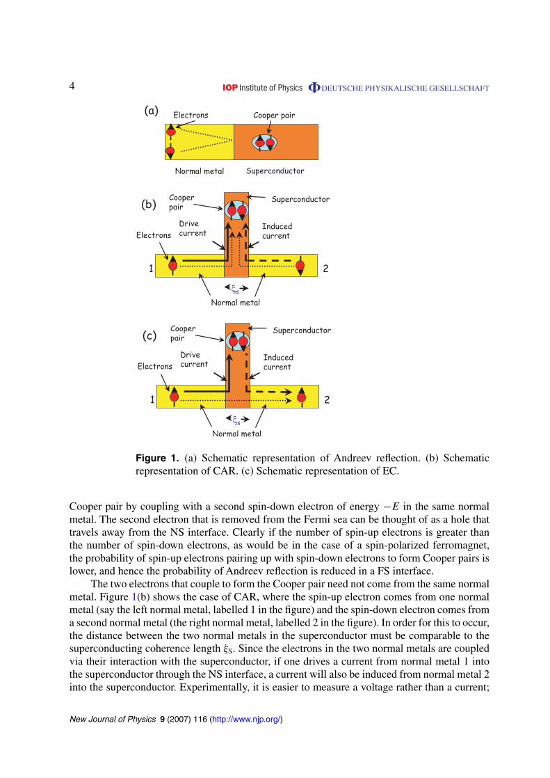
Figure 1(a) shows a schematic representation of conventional Andreev reflection: a spin-upelectron and energy E incident on a NS interface can propagate into the superconductor as a
1 An excellent review of proximity effects in superconductor-ferromagnet devices can be found in the reviewarticle [15].
New Journal of Physics 9 (2007) 116 (http://www.njp.org/)
4 DEUTSCHE PHYSIKALISCHE GESELLSCHAFT
Normal metal
Electrons Cooper pair
Superconductor
(a)
Superconductor
Normal metal
Electrons
Cooperpair
ξs
1 2
Drivecurrent
(b)
Inducedcurrent
Superconductor
Normal metal
Electrons
Cooperpair
ξs
1 2
Drivecurrent
(c)
Inducedcurrent
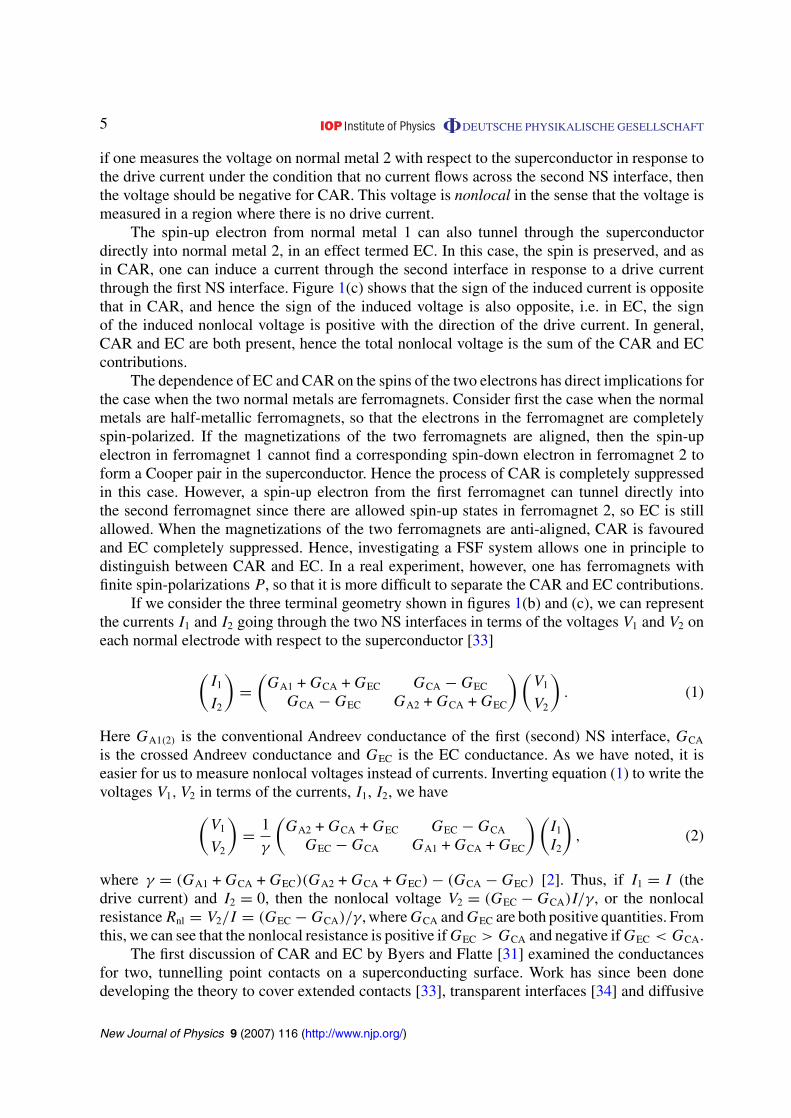
Figure 1. (a) Schematic representation of Andreev reflection. (b) Schematicrepresentation of CAR. (c) Schematic representation of EC.
Cooper pair by coupling with a second spin-down electron of energy −E in the same normalmetal. The second electron that is removed from the Fermi sea can be thought of as a hole thattravels away from the NS interface. Clearly if the number of spin-up electrons is greater thanthe number of spin-down electrons, as would be in the case of a spin-polarized ferromagnet,the probability of spin-up electrons pairing up with spin-down electrons to form Cooper pairs islower, and hence the probability of Andreev reflection is reduced in a FS interface.
The two electrons that couple to form the Cooper pair need not come from the same normalmetal. Figure 1(b) shows the case of CAR, where the spin-up electron comes from one normalmetal (say the left normal metal, labelled 1 in the figure) and the spin-down electron comes froma second normal metal (the right normal metal, labelled 2 in the figure). In order for this to occur,the distance between the two normal metals in the superconductor must be comparable to thesuperconducting coherence length ξS. Since the electrons in the two normal metals are coupledvia their interaction with the superconductor, if one drives a current from normal metal 1 intothe superconductor through the NS interface, a current will also be induced from normal metal 2into the superconductor. Experimentally, it is easier to measure a voltage rather than a current;
New Journal of Physics 9 (2007) 116 (http://www.njp.org/)
5 DEUTSCHE PHYSIKALISCHE GESELLSCHAFT
if one measures the voltage on normal metal 2 with respect to the superconductor in response tothe drive current under the condition that no current flows across the second NS interface, thenthe voltage should be negative for CAR. This voltage is nonlocal in the sense that the voltage ismeasured in a region where there is no drive current.
The spin-up electron from normal metal 1 can also tunnel through the superconductordirectly into normal metal 2, in an effect termed EC. In this case, the spin is preserved, and asin CAR, one can induce a current through the second interface in response to a drive currentthrough the first NS interface. Figure 1(c) shows that the sign of the induced current is oppositethat in CAR, and hence the sign of the induced voltage is also opposite, i.e. in EC, the signof the induced nonlocal voltage is positive with the direction of the drive current. In general,CAR and EC are both present, hence the total nonlocal voltage is the sum of the CAR and ECcontributions.
The dependence of EC and CAR on the spins of the two electrons has direct implications forthe case when the two normal metals are ferromagnets. Consider first the case when the normalmetals are half-metallic ferromagnets, so that the electrons in the ferromagnet are completelyspin-polarized. If the magnetizations of the two ferromagnets are aligned, then the spin-upelectron in ferromagnet 1 cannot find a corresponding spin-down electron in ferromagnet 2 toform a Cooper pair in the superconductor. Hence the process of CAR is completely suppressedin this case. However, a spin-up electron from the first ferromagnet can tunnel directly intothe second ferromagnet since there are allowed spin-up states in ferromagnet 2, so EC is stillallowed. When the magnetizations of the two ferromagnets are anti-aligned, CAR is favouredand EC completely suppressed. Hence, investigating a FSF system allows one in principle todistinguish between CAR and EC. In a real experiment, however, one has ferromagnets withfinite spin-polarizations P , so that it is more difficult to separate the CAR and EC contributions.
If we consider the three terminal geometry shown in figures 1(b) and (c), we can representthe currents I1 and I2 going through the two NS interfaces in terms of the voltages V1 and V2 oneach normal electrode with respect to the superconductor [33]
(I1
I2
)=
(GA1 + GCA + GEC GCA − GEC
GCA − GEC GA2 + GCA + GEC
) (V1
V2
). (1)
Here GA1(2) is the conventional Andreev conductance of the first (second) NS interface, GCA
is the crossed Andreev conductance and GEC is the EC conductance. As we have noted, it iseasier for us to measure nonlocal voltages instead of currents. Inverting equation (1) to write thevoltages V1, V2 in terms of the currents, I1, I2, we have
(V1
V2
)= 1
γ
(GA2 + GCA + GEC GEC − GCA
GEC − GCA GA1 + GCA + GEC
) (I1
I2
), (2)
where γ = (GA1 + GCA + GEC)(GA2 + GCA + GEC) − (GCA − GEC) [2]. Thus, if I1 = I (thedrive current) and I2 = 0, then the nonlocal voltage V2 = (GEC − GCA)I/γ , or the nonlocalresistance Rnl = V2/I = (GEC − GCA)/γ , where GCA and GEC are both positive quantities. Fromthis, we can see that the nonlocal resistance is positive if GEC > GCA and negative if GEC < GCA.
The first discussion of CAR and EC by Byers and Flatte [31] examined the conductancesfor two, tunnelling point contacts on a superconducting surface. Work has since been donedeveloping the theory to cover extended contacts [33], transparent interfaces [34] and diffusive
New Journal of Physics 9 (2007) 116 (http://www.njp.org/)
6 DEUTSCHE PHYSIKALISCHE GESELLSCHAFT
Normal metal Superconductor
I
µn
µµ
V+ V-
cp cp
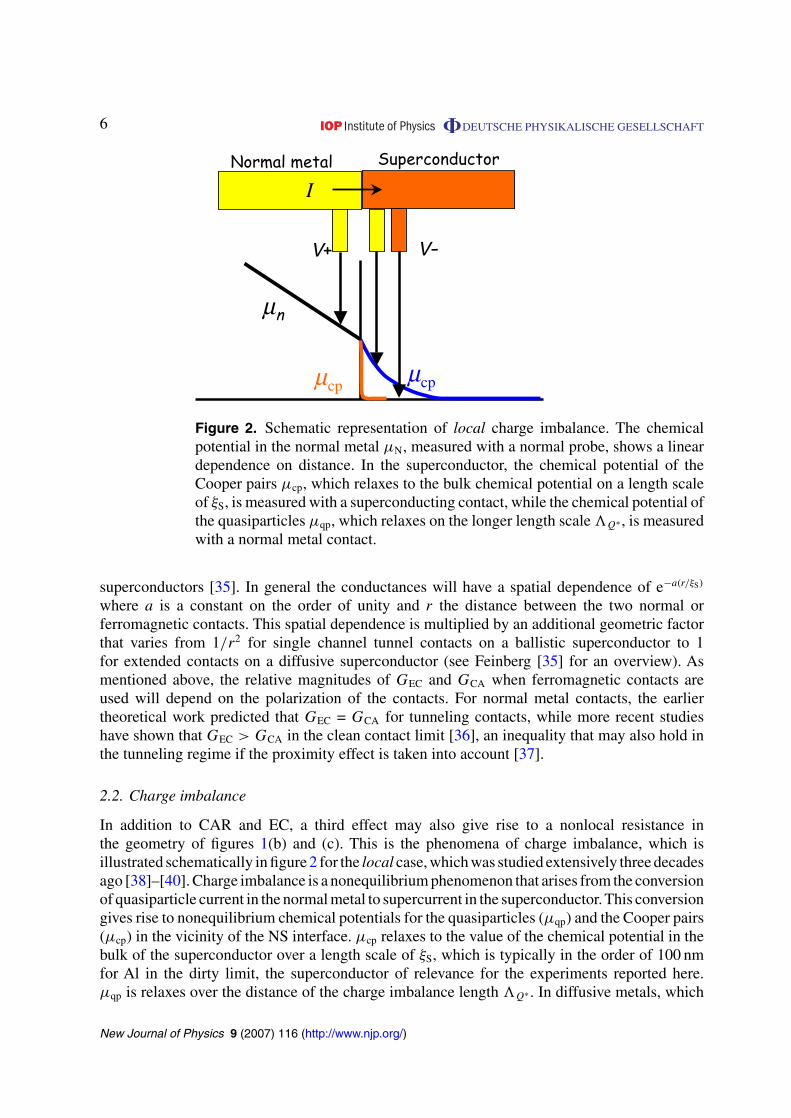
Figure 2. Schematic representation of local charge imbalance. The chemicalpotential in the normal metal µN, measured with a normal probe, shows a lineardependence on distance. In the superconductor, the chemical potential of theCooper pairs µcp, which relaxes to the bulk chemical potential on a length scaleof ξS, is measured with a superconducting contact, while the chemical potential ofthe quasiparticles µqp, which relaxes on the longer length scale Q∗ , is measuredwith a normal metal contact.
superconductors [35]. In general the conductances will have a spatial dependence of e−a(r/ξS)
where a is a constant on the order of unity and r the distance between the two normal orferromagnetic contacts. This spatial dependence is multiplied by an additional geometric factorthat varies from 1/r2 for single channel tunnel contacts on a ballistic superconductor to 1for extended contacts on a diffusive superconductor (see Feinberg [35] for an overview). Asmentioned above, the relative magnitudes of GEC and GCA when ferromagnetic contacts areused will depend on the polarization of the contacts. For normal metal contacts, the earliertheoretical work predicted that GEC = GCA for tunneling contacts, while more recent studieshave shown that GEC > GCA in the clean contact limit [36], an inequality that may also hold inthe tunneling regime if the proximity effect is taken into account [37].
2.2. Charge imbalance
In addition to CAR and EC, a third effect may also give rise to a nonlocal resistance inthe geometry of figures 1(b) and (c). This is the phenomena of charge imbalance, which isillustrated schematically in figure 2 for the local case, which was studied extensively three decadesago [38]–[40]. Charge imbalance is a nonequilibrium phenomenon that arises from the conversionof quasiparticle current in the normal metal to supercurrent in the superconductor. This conversiongives rise to nonequilibrium chemical potentials for the quasiparticles (µqp) and the Cooper pairs(µcp) in the vicinity of the NS interface. µcp relaxes to the value of the chemical potential in thebulk of the superconductor over a length scale of ξS, which is typically in the order of 100 nmfor Al in the dirty limit, the superconductor of relevance for the experiments reported here.µqp is relaxes over the distance of the charge imbalance length Q∗ . In diffusive metals, which
New Journal of Physics 9 (2007) 116 (http://www.njp.org/)

7 DEUTSCHE PHYSIKALISCHE GESELLSCHAFT
are the materials of interest here, the charge imbalance length is given by Q∗ = √DτQ∗ , where
D = (1/3)vF is the diffusion coefficient, is the elastic mean free path and the charge imbalancetime τQ∗ close to the superconducting transition has been modelled by [40]
τQ∗ = 4kBT
π(T)τin. (3)
Here (T) is the temperature dependent gap in the superconductor and τin is the electron inelasticscattering time. As T → Tc, (T) → 0 and τQ∗ and Q∗ diverge. Values of Q∗ in the orderof tens of microns have been measured in early experiments on phase slip centres very closeto the superconducting transition in Al [41]–[43]. Thus Q∗ is typically larger than ξS in theexperiments performed to date.
The spatial dependence of µqp near the NS interface is given by [44]
µqp = eQ∗ρAlI tanh(x/Q∗), (4)
where x is the distance from the NS interface into the superconductor and ρAl is the resistanceper unit length of the Al wire. This is the chemical potential measured by a normal metal probe.If a superconducting probe were placed at the same position x, it would measure µcp, whichfor distances x > ξS is essentially the chemical potential in the bulk of the superconductor.The bulk value of the chemical potential can be determined by taking the asymptotic value ofµqp for x Q∗ , which is simply eQ∗ρAlI. Thus, the voltage difference measured betweena superconducting probe and a normal probe placed a distance x from the interface is justV = Q∗ρAlI[1 − tanh(x/Q∗)], giving rise to a resistance
R(x) = Q∗ρAl[1 − tanh(x/Q∗)]. (5)
It should be emphasized that since µcp reaches the value in the bulk of the superconductor forx > ξS, the resistance measured between the normal voltage probe at x and any superconductingprobe at a distance x > ξS would measure the same R(x).
When the superconductor is normal, a voltage probe made from a superconducting materialplaced at a distance x > ξS from the interface would measure a linearly varying potentialµN(x) = eρAlIx, while the same probe below the superconducting transition would measurethe bulk chemical superconducting potential that we have just shown is eρAlIQ∗ . Thus, asuperconducting probe would measure an enhancement of the resistance of the NS interfaceover the normal state resistance RN by an amount
Rint(x) = (Q∗ − x)ρAl. (6)
Since Q∗ diverges at the superconducting transition, this resistance enhancement should bemaximum at the transition, and decay as the temperature is decreased below Tc. Enhancementsof the normal state resistance near the superconducting transition have been seen in a numberof experiments on NS interfaces and phase slip centres [45, 46]. However, the resistanceenhancement observed is typically in the order of 0.2–0.4 RN, where RN is the normal stateresistance of the interface. This should be compared to the resistance enhancements of 5–20 RN
expected if Q∗ is of the order of 10–40 microns as reported in earlier experiments [41]–[43].If equation (6) is correct, our estimates of Q∗ based on these recent experiments must be revisedto values of the order of 1µm in Al.
New Journal of Physics 9 (2007) 116 (http://www.njp.org/)
8 DEUTSCHE PHYSIKALISCHE GESELLSCHAFT
It must be emphasized that the foregoing description of charge imbalance in the electricaltransport of NS interfaces is for the local case. To our knowledge, there is no theoreticaldescription yet of charge imbalance in the nonlocal case, by which we mean a geometry similarto that of figures 1(b) and (c), where no current flows through the interface through which thepotential is being measured by a normal metal probe. However, it is reasonable to assume that ifa charge imbalance is created at the first NS interface through which a current is being driven, itwill decay over some length scale in all directions into the superconductor. The length scale overwhich it decays may be different depending on whether a current is present, so that the effectivecharge imbalance length may be different in the nonlocal case. In addition, the charge imbalancelength would conceivably be modified if the quasiparticle current injected into the superconductorwere spin polarized (in the case when the normal metal is a ferromagnet), since the relaxation timewould also involve the polarization of the quasiparticles in the superconductor. In either case, thenonlocal voltage measured on the second normal metal probe with respect to the superconductorwould be positive, i.e. of the same sign as the contribution due EC, and opposite that due toCAR. The decay length of charge imbalance and EC/CAR as a function of distance between thetwo interfaces is expected to be different: while EC and CAR contributions decay exponentiallyon the length scale of ξS, the decay length of the charge imbalance contribution based on ourknowledge of the local case might be expected to decay on a length scale comparable to Q∗ ,with a spatial dependence given by equation (5).
In summary, we note here again for reference the sign of the three potential contributions tothe nonlocal signal in FSF and NSN structures: CAR, EC and charge imbalance. With referenceto the sample geometry of figure 1(b) or (c), with a drive current being driven from the firstnormal metal and the superconductor and the nonlocal voltage being measured between thesecond normal metal and the same superconductor, EC and charge imbalance would give riseto a positive nonlocal voltage, while CAR would give rise to a negative nonlocal voltage. Thedifferent signs of the effects, coupled with their different spatial dependences give us in principlethe potential to distinguish experimentally between them.
3. Experimental techniques: fabrication and measurement
3.1. Fabrication
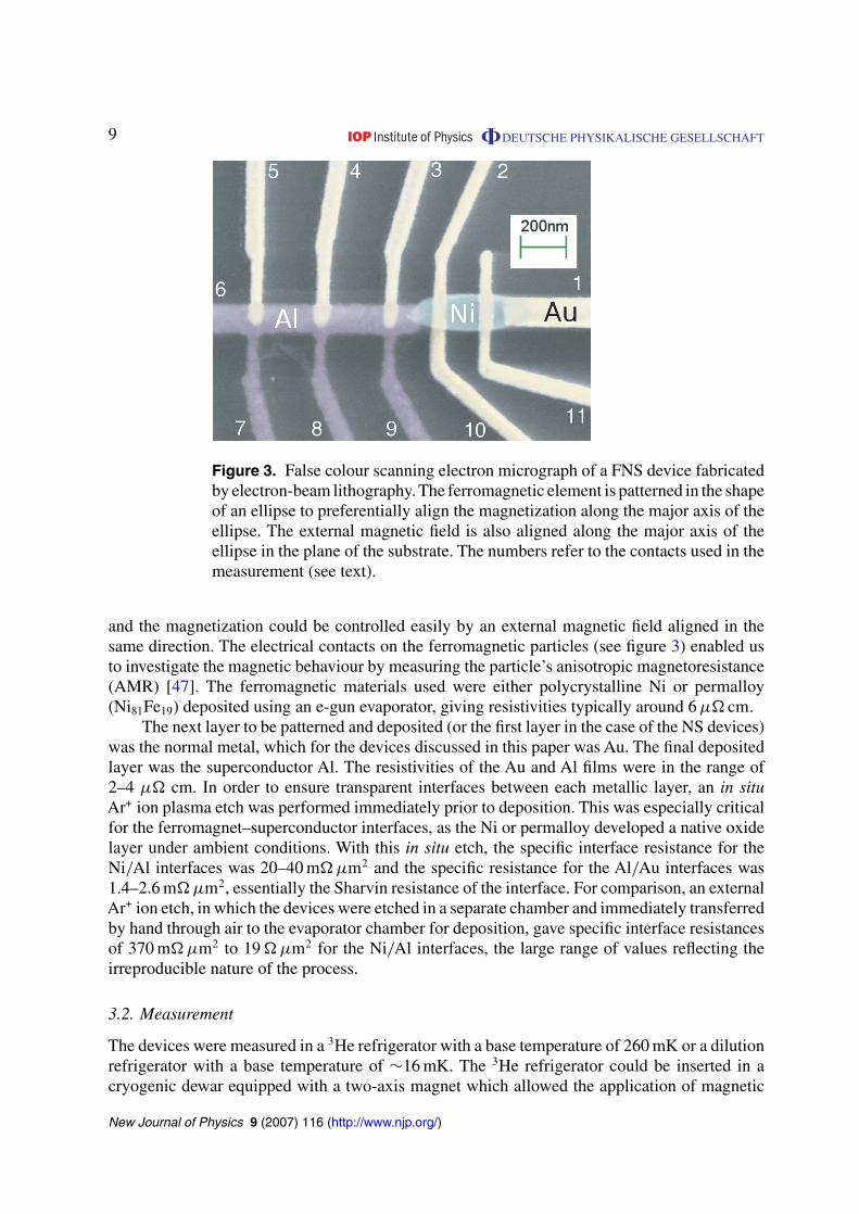
All the devices discussed in this paper were patterned using conventional electron beamlithography using a JEOL 840 scanning electron microscope converted for e-beam writing.The substrates were oxidized Si wafers. Figure 3 shows an example of a ferromagnet/normal-metal/superconductor device. Since all the devices consist of at least two to three differentmaterials, multilevel patterning was essential. Our electron-beam lithography software allows usto align features on different lithography levels on the devices to better than 20 nm, and in somecases better than 10 nm. For devices incorporating ferromagnetic materials, the ferromagnet wasthe first layer of the device to be patterned. This was to ensure that the ferromagnetic material layflat on the substrate surface; if the ferromagnet were to be placed on either the normal metal orsuperconducting elements of the device, the resulting uneven film profile would be more likelyto nucleate ferromagnetic domain structure. For the same reason, the ferromagnetic materialswere patterned in the form of ellipses, as our previous studies [47] indicated that this shapeprofile was likely to orient the magnetization preferentially along the major axis of the ellipse
New Journal of Physics 9 (2007) 116 (http://www.njp.org/)
9 DEUTSCHE PHYSIKALISCHE GESELLSCHAFT
Figure 3. False colour scanning electron micrograph of a FNS device fabricatedby electron-beam lithography. The ferromagnetic element is patterned in the shapeof an ellipse to preferentially align the magnetization along the major axis of theellipse. The external magnetic field is also aligned along the major axis of theellipse in the plane of the substrate. The numbers refer to the contacts used in themeasurement (see text).
and the magnetization could be controlled easily by an external magnetic field aligned in thesame direction. The electrical contacts on the ferromagnetic particles (see figure 3) enabled usto investigate the magnetic behaviour by measuring the particle’s anisotropic magnetoresistance(AMR) [47]. The ferromagnetic materials used were either polycrystalline Ni or permalloy(Ni81Fe19) deposited using an e-gun evaporator, giving resistivities typically around 6 µ cm.
The next layer to be patterned and deposited (or the first layer in the case of the NS devices)was the normal metal, which for the devices discussed in this paper was Au. The final depositedlayer was the superconductor Al. The resistivities of the Au and Al films were in the range of2–4 µ cm. In order to ensure transparent interfaces between each metallic layer, an in situAr+ ion plasma etch was performed immediately prior to deposition. This was especially criticalfor the ferromagnet–superconductor interfaces, as the Ni or permalloy developed a native oxidelayer under ambient conditions. With this in situ etch, the specific interface resistance for theNi/Al interfaces was 20–40 m µm2 and the specific resistance for the Al/Au interfaces was1.4–2.6 m µm2, essentially the Sharvin resistance of the interface. For comparison, an externalAr+ ion etch, in which the devices were etched in a separate chamber and immediately transferredby hand through air to the evaporator chamber for deposition, gave specific interface resistancesof 370 m µm2 to 19 µm2 for the Ni/Al interfaces, the large range of values reflecting theirreproducible nature of the process.
3.2. Measurement
The devices were measured in a 3He refrigerator with a base temperature of 260 mK or a dilutionrefrigerator with a base temperature of ∼16 mK. The 3He refrigerator could be inserted in acryogenic dewar equipped with a two-axis magnet which allowed the application of magnetic
New Journal of Physics 9 (2007) 116 (http://www.njp.org/)
10 DEUTSCHE PHYSIKALISCHE GESELLSCHAFT
fields both in the plane of the sample substrate and perpendicular to the sample substrate. Sincethe application of a magnetic field along the axis of the elliptical ferromagnets was essential, allthe devices incorporating ferromagnetic elements were measured using the 3He refrigerator. Thecryostat of the dilution refrigerator was equipped with a large axial superconducting magnet,although only small magnetic fields were required for these experiments. Both refrigerators werewell-shielded against interference from rf and line frequency sources.
Local and non-local four terminal resistance measurements2 were performed using home-made, ac Adler–Jackson type resistance bridges operating at frequencies in the range of11–200 Hz. By using multiple bridges operating at different frequencies, we were in principle ableto simultaneously measure the resistances of multiple sections of a single device. In practice,equipment space considerations limited us to two simultaneous resistance measurements. Acexcitation currents were typically in the range of 20–200 nA in order to avoid self-heating.For the local and nonlocal four-terminal differential resistance measurements, a dc current wasapplied between two of the contacts on the device using a home-made current source with anoutput impedance greater than 1012 . The remaining part of the measurement circuit couldbe kept the same, enabling us to measure the simultaneous four-terminal differential resistancedV/dI as a function of dc current Idc for two different sections of a single device. Given thenumber of contacts, we shall adopt the now standard notation for four-terminal measurements:R1,2;3,4 denotes the four-terminal resistance where the current is introduced through contact 1(I+) and removed through contact 2 (I−) and the voltage is measured across contacts 3 and 4(V + and V− respectively). For the differential resistance, we shall adopt the same notation, i.e.R1,2;3,4 denotes dV3,4/dI1,2, where it will be clear from the context whether we are referring toa zero-bias resistance or a differential resistance as a function of dc current. For the differentialresistance measurements, it is necessary to also give the path of the dc current Idc; this will begiven explicitly for each case.
4. Experimental results
4.1. Ferromagnet/superconductor/normal-metal structures
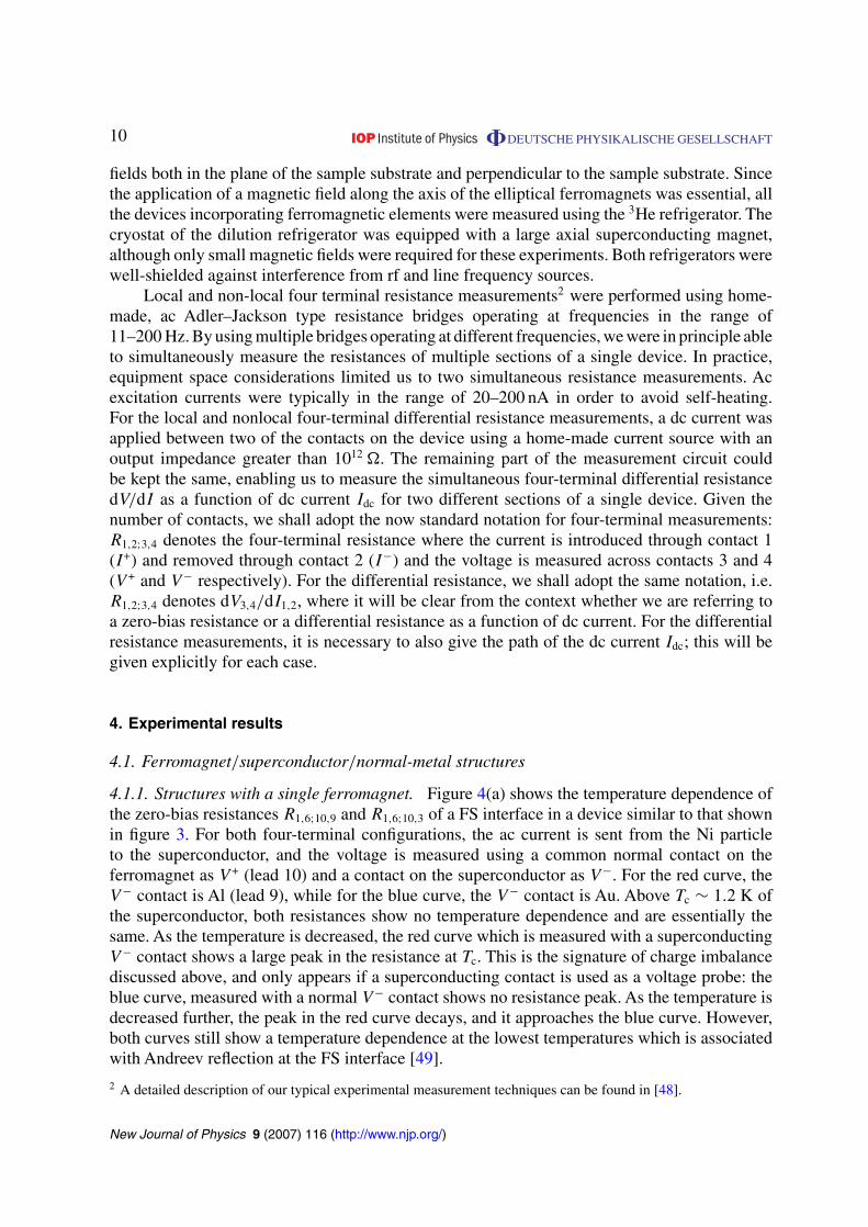
4.1.1. Structures with a single ferromagnet. Figure 4(a) shows the temperature dependence ofthe zero-bias resistances R1,6;10,9 and R1,6;10,3 of a FS interface in a device similar to that shownin figure 3. For both four-terminal configurations, the ac current is sent from the Ni particleto the superconductor, and the voltage is measured using a common normal contact on theferromagnet as V + (lead 10) and a contact on the superconductor as V−. For the red curve, theV− contact is Al (lead 9), while for the blue curve, the V− contact is Au. Above Tc ∼ 1.2 K ofthe superconductor, both resistances show no temperature dependence and are essentially thesame. As the temperature is decreased, the red curve which is measured with a superconductingV− contact shows a large peak in the resistance at Tc. This is the signature of charge imbalancediscussed above, and only appears if a superconducting contact is used as a voltage probe: theblue curve, measured with a normal V− contact shows no resistance peak. As the temperature isdecreased further, the peak in the red curve decays, and it approaches the blue curve. However,both curves still show a temperature dependence at the lowest temperatures which is associatedwith Andreev reflection at the FS interface [49].
2 A detailed description of our typical experimental measurement techniques can be found in [48].
New Journal of Physics 9 (2007) 116 (http://www.njp.org/)
11 DEUTSCHE PHYSIKALISCHE GESELLSCHAFT
8.5
9.0
9.5
10.0
10.5
11.0
11.5
12.0
Res
ista
nce
(Ω)
(a)
0
0.5
1.0
1.5
2.0
2.5
0.2 0.4 0.6 0.8 1.0 1.2 1.4 1.6 1.8
∆ R
(Ω
)
Temperature (K)
(b)
Figure 4. Temperature dependence of the zero-bias resistance of a device similarto that shown in figure 3. (a) Red curve R1,6;10,9, blue curve R1,6;10,3. (b) Thedifference of the two curves in (a), which corresponds to the four-terminalresistance R1,6;3,9.
In order to eliminate the temperature dependence of the interface, one can subtract theblue curve from the red curve, which corresponds to measuring the four-terminal resistanceR1,6;3,9. Since the superconducting contact (lead 9) and the normal-metal contact (lead 3) areeffectively measuring the potential at the same distance from the FS interface, classically onemight expect the measured resistance to vanish. As can be seen in figure 4(b), this is essentiallywhat occurs above Tc; the difference in resistance is zero. Below Tc, however, a large peakappears. Comparison to the schematic in figure 2 shows that what is being measured is thedifference between µqp and µcp at the same point, i.e. the peak in figure 4(b) is a pure chargeimbalance effect. As the temperature is decreased further, the charge imbalance contributiondecreases and appears to vanish, although there is some indication of a small but finite resistanceeven at the lowest temperatures, a potential contribution from CAR and EC. We note that themagnitude of the resistance enhancement is ∼ 1.65 . From equation (6), the enhancement of theresistance over the normal state resistance is ρAl(Q∗ − x). For this sample, ρAl = 5.6 /µm−1
and x = 110 nm, giving Q∗ = 0.41 µm, far smaller than the values found in the early studieson charge imbalance in Al.
New Journal of Physics 9 (2007) 116 (http://www.njp.org/)
12 DEUTSCHE PHYSIKALISCHE GESELLSCHAFT
−4
−2
0
2
4
R1,6;3,9
R1,6;4,8
R1,6;5,7
Diff
eren
tial r
esis
tanc
e (Ω
)
(a)
−15
−10
−5
0
5
10
15
0 5 10 15 20
R1,6;3,9
R1,6;4,8
scaled
R1,6;5,7
scaled
(b)
I dc (µA)
Figure 5. (a) Four-terminal differential resistance of three pairs ofAuAl contacts,R1,6;3,9, R1,6;4,8 and R1,6;5,7 at T = 260 mK, with Idc introduced through contact 1and removed through contact 6. (See figure 3 for sample geometry.) (b) Same asin (a), but with R1,6;4,8 and R1,6;5,7 scaled by 1.96 and 4.05 respectively to matchR1,6;3,9 below Idc = 12 µA.
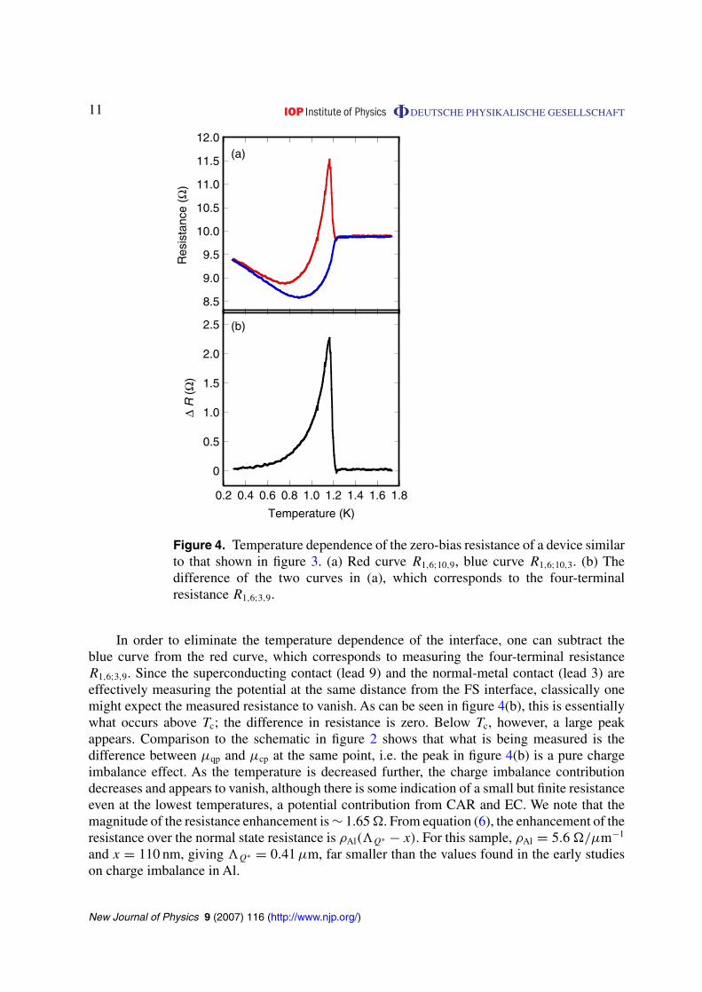
A similar dependence can be observed in the differential resistance dV/dI as function of Idc.Figure 5(a) shows differential resistances R1,6;3,9, R1,6;4,8 and R1,6;5,7 corresponding to the threesuccessive pairs of complementary Au/Al contacts along the superconducting wire in figure 3.The shape of the R versus. Idc curve for Idc ≤ 12 µA is similar to the R versus T curve for T Tc.Near zero bias Idc = 0, the resistance for all three curves is essentially 0, but rises monotonicallyuntil Idc ∼ 12 µA, except for a sharp peak at around 7.63 µA. This contribution to the differentialresistance decreases as one goes further away from the FS interface. The similarity in shape inthis current regime to the temperature dependent resistance shown in figure 4 suggests that thiscontribution is due to charge imbalance. If we scale the R1,6;4,8 and R1,6;5,7 curves, we can matchthe R1,6;3,9 curve in the range 0 Idc 12 µA, as shown in figure 5(b). A fit of the inverse scalefactors as a function of distance from the FS interface to the functional form in equation (5) givesa value for Q∗ of 0.64µm, in good agreement our rough estimate obtained from the temperaturedependence in figure 4. It should be noted that the peaks at Idc = 7.63 µA in all three curves alsomatch with these same scaling factors, indicating that they might be also associated with chargeimbalance, although their origin is not clear to us at present.
New Journal of Physics 9 (2007) 116 (http://www.njp.org/)
13 DEUTSCHE PHYSIKALISCHE GESELLSCHAFT
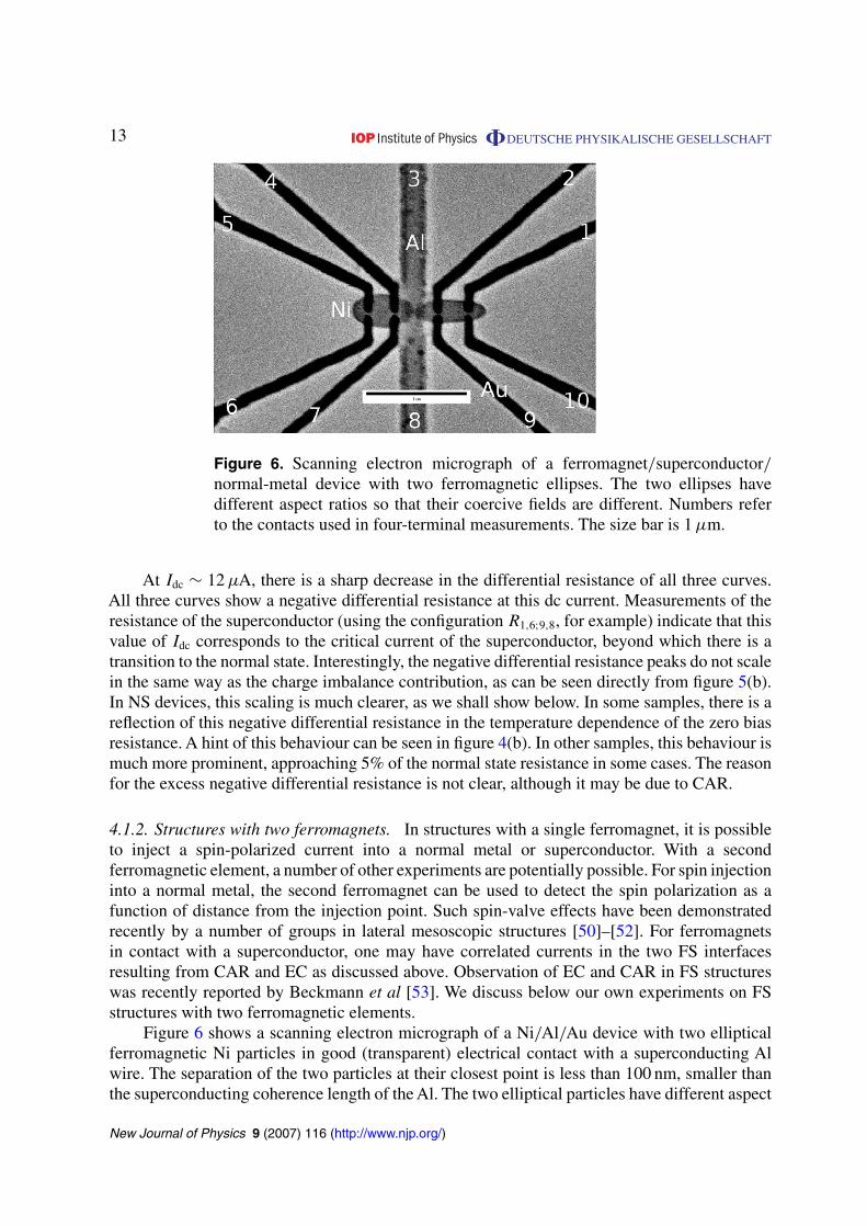
Figure 6. Scanning electron micrograph of a ferromagnet/superconductor/normal-metal device with two ferromagnetic ellipses. The two ellipses havedifferent aspect ratios so that their coercive fields are different. Numbers referto the contacts used in four-terminal measurements. The size bar is 1 µm.
At Idc ∼ 12 µA, there is a sharp decrease in the differential resistance of all three curves.All three curves show a negative differential resistance at this dc current. Measurements of theresistance of the superconductor (using the configuration R1,6;9,8, for example) indicate that thisvalue of Idc corresponds to the critical current of the superconductor, beyond which there is atransition to the normal state. Interestingly, the negative differential resistance peaks do not scalein the same way as the charge imbalance contribution, as can be seen directly from figure 5(b).In NS devices, this scaling is much clearer, as we shall show below. In some samples, there is areflection of this negative differential resistance in the temperature dependence of the zero biasresistance. A hint of this behaviour can be seen in figure 4(b). In other samples, this behaviour ismuch more prominent, approaching 5% of the normal state resistance in some cases. The reasonfor the excess negative differential resistance is not clear, although it may be due to CAR.
4.1.2. Structures with two ferromagnets. In structures with a single ferromagnet, it is possibleto inject a spin-polarized current into a normal metal or superconductor. With a secondferromagnetic element, a number of other experiments are potentially possible. For spin injectioninto a normal metal, the second ferromagnet can be used to detect the spin polarization as afunction of distance from the injection point. Such spin-valve effects have been demonstratedrecently by a number of groups in lateral mesoscopic structures [50]–[52]. For ferromagnetsin contact with a superconductor, one may have correlated currents in the two FS interfacesresulting from CAR and EC as discussed above. Observation of EC and CAR in FS structureswas recently reported by Beckmann et al [53]. We discuss below our own experiments on FSstructures with two ferromagnetic elements.
Figure 6 shows a scanning electron micrograph of a Ni/Al/Au device with two ellipticalferromagnetic Ni particles in good (transparent) electrical contact with a superconducting Alwire. The separation of the two particles at their closest point is less than 100 nm, smaller thanthe superconducting coherence length of the Al. The two elliptical particles have different aspect
New Journal of Physics 9 (2007) 116 (http://www.njp.org/)
14 DEUTSCHE PHYSIKALISCHE GESELLSCHAFT
1.268
1.270
1.272
1.274
1.276
1.278
R 5
,8;6
,7 (
Ω)
(a)
−0.176
−0.175
−0.174
−0.173
R 5
,8;1
0,3
(Ω)
(b)
5.365
5.370
5.375
5.380
5.385
5.390
5.395
−1200−800 −400 0 400 800 1200
R 6
,10;
7,9
(Ω)
H(Oe)
(c)
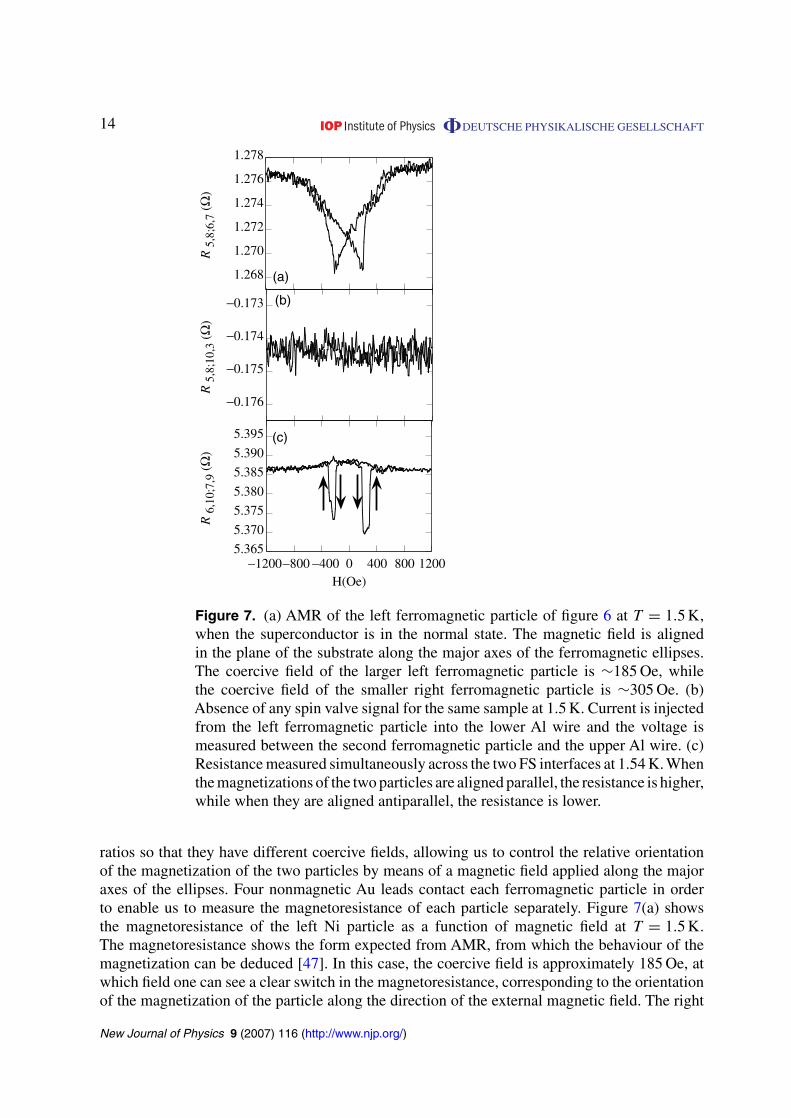
Figure 7. (a) AMR of the left ferromagnetic particle of figure 6 at T = 1.5 K,when the superconductor is in the normal state. The magnetic field is alignedin the plane of the substrate along the major axes of the ferromagnetic ellipses.The coercive field of the larger left ferromagnetic particle is ∼185 Oe, whilethe coercive field of the smaller right ferromagnetic particle is ∼305 Oe. (b)Absence of any spin valve signal for the same sample at 1.5 K. Current is injectedfrom the left ferromagnetic particle into the lower Al wire and the voltage ismeasured between the second ferromagnetic particle and the upper Al wire. (c)Resistance measured simultaneously across the two FS interfaces at 1.54 K. Whenthe magnetizations of the two particles are aligned parallel, the resistance is higher,while when they are aligned antiparallel, the resistance is lower.
ratios so that they have different coercive fields, allowing us to control the relative orientationof the magnetization of the two particles by means of a magnetic field applied along the majoraxes of the ellipses. Four nonmagnetic Au leads contact each ferromagnetic particle in orderto enable us to measure the magnetoresistance of each particle separately. Figure 7(a) showsthe magnetoresistance of the left Ni particle as a function of magnetic field at T = 1.5 K.The magnetoresistance shows the form expected from AMR, from which the behaviour of themagnetization can be deduced [47]. In this case, the coercive field is approximately 185 Oe, atwhich field one can see a clear switch in the magnetoresistance, corresponding to the orientationof the magnetization of the particle along the direction of the external magnetic field. The right
New Journal of Physics 9 (2007) 116 (http://www.njp.org/)
15 DEUTSCHE PHYSIKALISCHE GESELLSCHAFT
ferromagnetic particle has a similar AMR signature with a larger coercive field of 305 Oe as ithas a longer aspect ratio.
With the information on the coercive field of each particle, one can manipulate the relativeorientations of magnetizations of the two particles to be either parallel or antiparallel by simplyvarying the external magnetic field. Figure 7(b) shows the nonlocal resistance measurement of thedevice of figure 6 measured with the superconductor in the normal state (T = 1.5 K) as a functionof magnetic field applied along the major axes of the elliptical particles. The current is sent fromthe left ferromagnetic particle into the lower Al contact, and the nonlocal voltage is measuredbetween the second ferromagnetic particle and the upper Al contact. This is the configuration inwhich one expects to see a spin-valve signal, i.e. a difference in the nonlocal resistance dependingon whether the magnetizations of the particles are aligned parallel or antiparallel, with the parallelconfiguration expected to have a larger resistance [50]–[52]. In our samples, no such spin-valvesignal is observed. Instead, if we measure the resistance across both FS interfaces, as shown infigure 7(c), one sees a signature reminiscent of a spin-valve device: for example, as the externalmagnetic field is increased from −1200 Oe, the resistance switches from a higher resistance to alower resistance at the coercive field of the left ferromagnetic particle and then switches back tothe higher resistance state at the coercive field of the right ferromagnetic particle. One may thinkthat this behaviour is just a reflection of the AMR of each individual particle. However, if this asthe case, one would observe a decrease in resistance before the coercive field of each particle isreached followed by a sharp increase in resistance, as seen in figure 7(a). This is clearly not whatis observed in figure 7(c). We posit that the absence of a spin-valve signature in figure 7(b) in theclassical spin configuration may be due to the small separation between the two ferromagneticparticles, which does not allow a spin-valve signal to develop sufficiently.
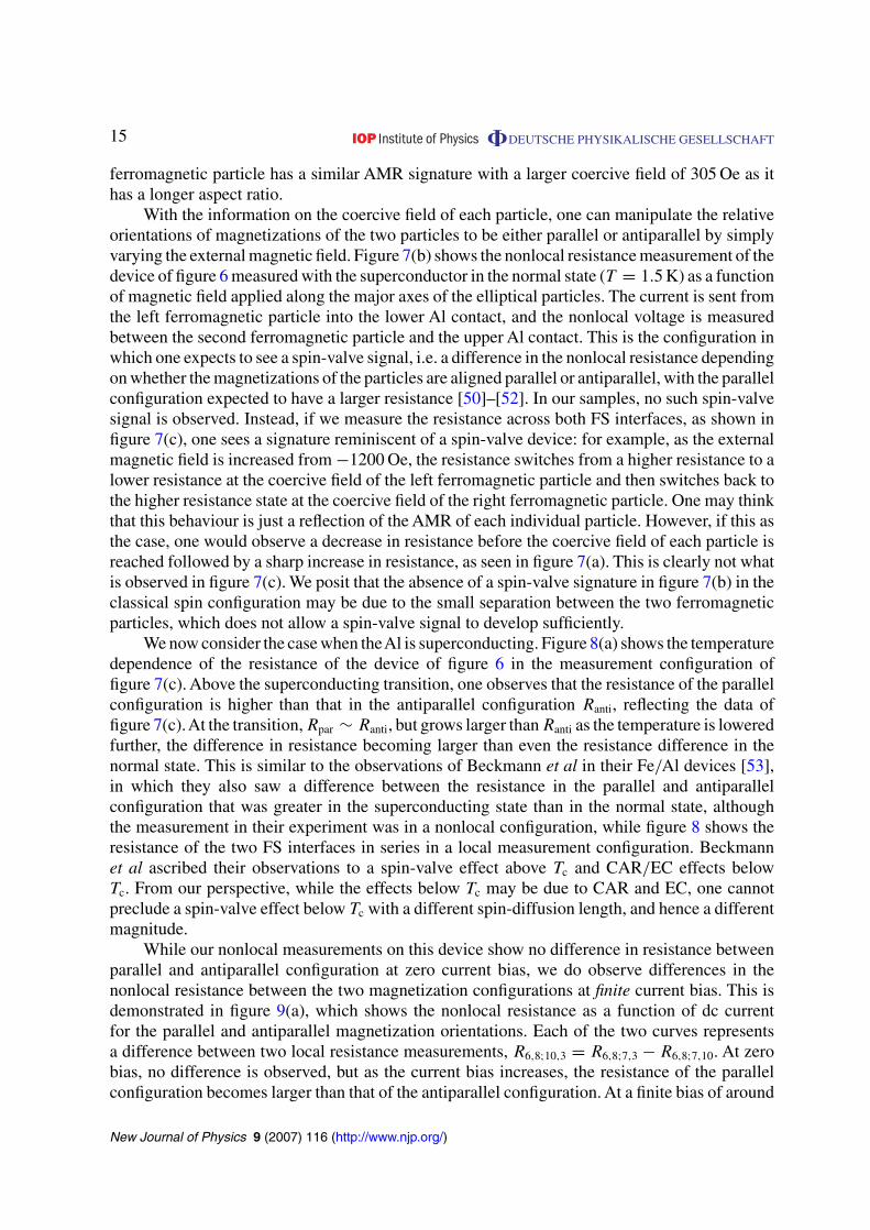
We now consider the case when theAl is superconducting. Figure 8(a) shows the temperaturedependence of the resistance of the device of figure 6 in the measurement configuration offigure 7(c). Above the superconducting transition, one observes that the resistance of the parallelconfiguration is higher than that in the antiparallel configuration Ranti, reflecting the data offigure 7(c).At the transition, Rpar ∼ Ranti, but grows larger than Ranti as the temperature is loweredfurther, the difference in resistance becoming larger than even the resistance difference in thenormal state. This is similar to the observations of Beckmann et al in their Fe/Al devices [53],in which they also saw a difference between the resistance in the parallel and antiparallelconfiguration that was greater in the superconducting state than in the normal state, althoughthe measurement in their experiment was in a nonlocal configuration, while figure 8 shows theresistance of the two FS interfaces in series in a local measurement configuration. Beckmannet al ascribed their observations to a spin-valve effect above Tc and CAR/EC effects belowTc. From our perspective, while the effects below Tc may be due to CAR and EC, one cannotpreclude a spin-valve effect below Tc with a different spin-diffusion length, and hence a differentmagnitude.
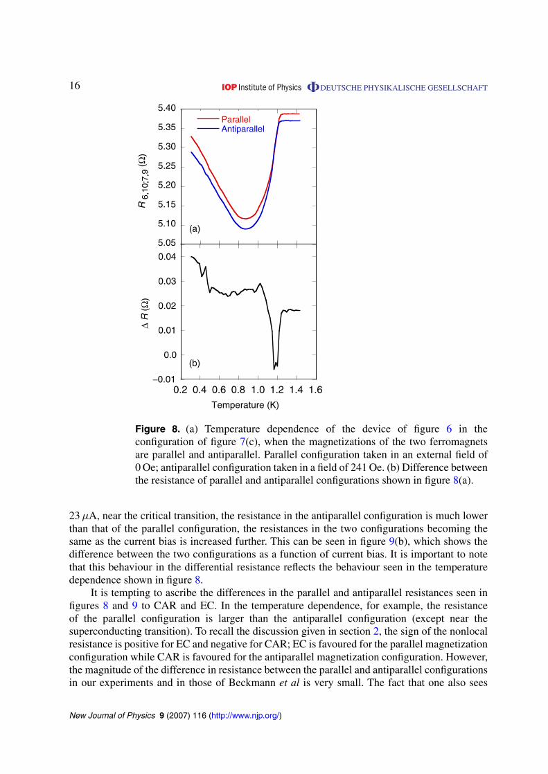
While our nonlocal measurements on this device show no difference in resistance betweenparallel and antiparallel configuration at zero current bias, we do observe differences in thenonlocal resistance between the two magnetization configurations at finite current bias. This isdemonstrated in figure 9(a), which shows the nonlocal resistance as a function of dc currentfor the parallel and antiparallel magnetization orientations. Each of the two curves representsa difference between two local resistance measurements, R6,8;10,3 = R6,8;7,3 − R6,8;7,10. At zerobias, no difference is observed, but as the current bias increases, the resistance of the parallelconfiguration becomes larger than that of the antiparallel configuration. At a finite bias of around
New Journal of Physics 9 (2007) 116 (http://www.njp.org/)
16 DEUTSCHE PHYSIKALISCHE GESELLSCHAFT
5.05
5.10
5.15
5.20
5.25
5.30
5.35
5.40ParallelAntiparallel
(a)
R 6
,10;
7,9
(Ω)
−0.01
0.0
0.01
0.02
0.03
0.04
0.2 0.4 0.6 0.8 1.0 1.2 1.4 1.6
∆ R
(Ω
)
Temperature (K)
(b)
Figure 8. (a) Temperature dependence of the device of figure 6 in theconfiguration of figure 7(c), when the magnetizations of the two ferromagnetsare parallel and antiparallel. Parallel configuration taken in an external field of0 Oe; antiparallel configuration taken in a field of 241 Oe. (b) Difference betweenthe resistance of parallel and antiparallel configurations shown in figure 8(a).
23 µA, near the critical transition, the resistance in the antiparallel configuration is much lowerthan that of the parallel configuration, the resistances in the two configurations becoming thesame as the current bias is increased further. This can be seen in figure 9(b), which shows thedifference between the two configurations as a function of current bias. It is important to notethat this behaviour in the differential resistance reflects the behaviour seen in the temperaturedependence shown in figure 8.
It is tempting to ascribe the differences in the parallel and antiparallel resistances seen infigures 8 and 9 to CAR and EC. In the temperature dependence, for example, the resistanceof the parallel configuration is larger than the antiparallel configuration (except near thesuperconducting transition). To recall the discussion given in section 2, the sign of the nonlocalresistance is positive for EC and negative for CAR; EC is favoured for the parallel magnetizationconfiguration while CAR is favoured for the antiparallel magnetization configuration. However,the magnitude of the difference in resistance between the parallel and antiparallel configurationsin our experiments and in those of Beckmann et al is very small. The fact that one also sees
New Journal of Physics 9 (2007) 116 (http://www.njp.org/)
17 DEUTSCHE PHYSIKALISCHE GESELLSCHAFT
−1.5
−1.0
−0.5
0.0
0.5
1.0
Non
loca
l res
ista
nce
(Ω)
(a)
−2.0
−1.5
−1.0
−0.5
0.0
0.5
−40 −30 −20 −10 0 10 20 30 40
ParallelAntiparallel
Parallel–antiparallel
I (µA)
(b)
Figure 9. (a) Difference of two differential resistance measurements of the NSinterface, R6,8;10,3 = R6,8;7,3 − R6,8;7,10, as a function of dc current, I6,8, of thedevice of figure 6 when the magnetizations of the two ferromagnets are parallel andantiparallel. Parallel configuration taken in an external field of 0 Oe; antiparallelconfiguration taken in a field of 241 Oe. (b) Difference between the differentialresistance of parallel and antiparallel configurations shown in figure 9(a).
a resistance difference above Tc leaves open the possibility that the effect below Tc may alsobe a spin-valve effect. In the case of the differential resistance (figure 9), the effect seemsto be more likely to be related to superconductivity since the largest differences between theantiparallel and parallel configurations occur near the superconducting transition. However, itmust be remembered that associated with each ferromagnetic element in these devices is alocal magnetic field, so that the total magnetic field on the superconductor in the parallel andantiparallel configurations may not be the same even when the externally applied magnetic fieldis the same. It is therefore very hard to deconvolute the different potential contributions to theresistance difference in FS structures, especially since the effect is relatively small. It is for thisreason that we have also measured NS structures without ferromagnets, where the effects due toCAR and EC are much larger. We discuss the results from these samples in the next section.
New Journal of Physics 9 (2007) 116 (http://www.njp.org/)
18 DEUTSCHE PHYSIKALISCHE GESELLSCHAFT
0
1
2
3
4
5
0 0.2 0.4 0.6 0.8 1.0 1.2 1.4
R(Ω
)
T(K)
(a)
−20
−15
−10
−5
0
5
0 2 4 6 8 10 12 14
R(Ω
)
Idc (µA)
(b)
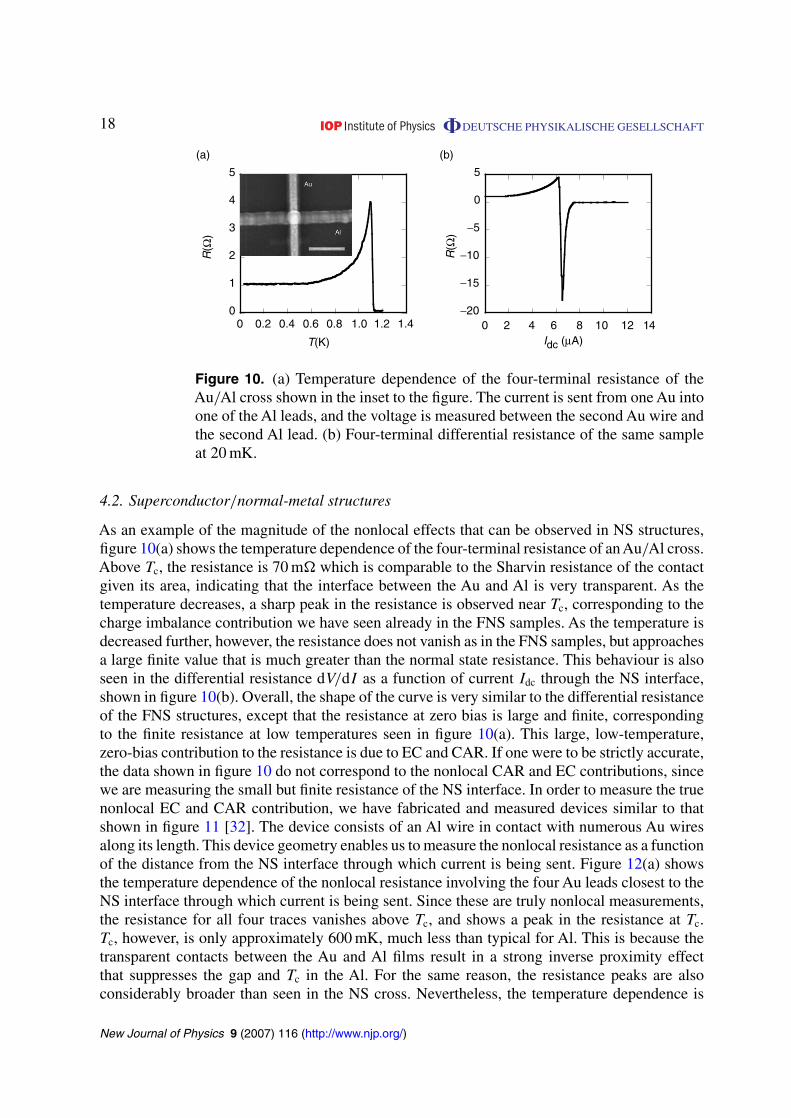
Figure 10. (a) Temperature dependence of the four-terminal resistance of theAu/Al cross shown in the inset to the figure. The current is sent from one Au intoone of the Al leads, and the voltage is measured between the second Au wire andthe second Al lead. (b) Four-terminal differential resistance of the same sampleat 20 mK.
4.2. Superconductor/normal-metal structures
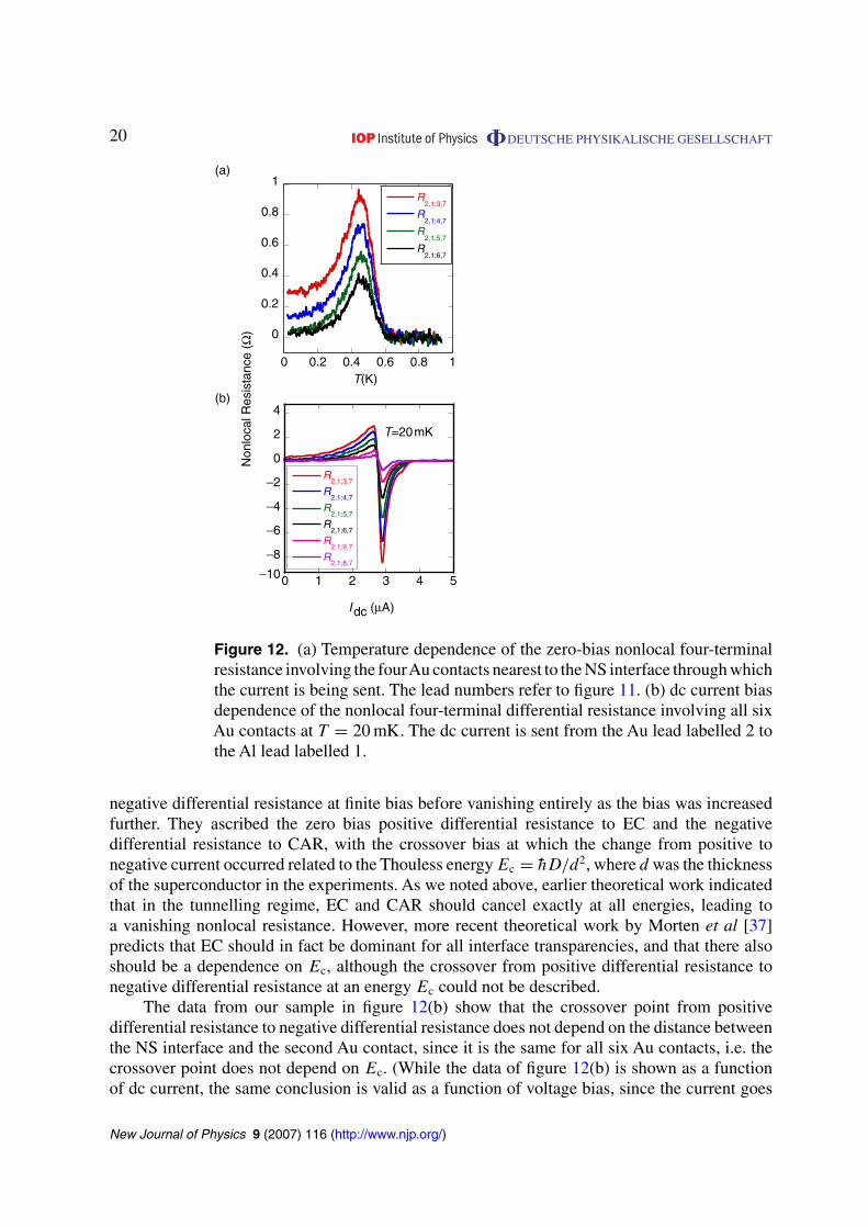
As an example of the magnitude of the nonlocal effects that can be observed in NS structures,figure 10(a) shows the temperature dependence of the four-terminal resistance of an Au/Al cross.Above Tc, the resistance is 70 m which is comparable to the Sharvin resistance of the contactgiven its area, indicating that the interface between the Au and Al is very transparent. As thetemperature decreases, a sharp peak in the resistance is observed near Tc, corresponding to thecharge imbalance contribution we have seen already in the FNS samples. As the temperature isdecreased further, however, the resistance does not vanish as in the FNS samples, but approachesa large finite value that is much greater than the normal state resistance. This behaviour is alsoseen in the differential resistance dV/dI as a function of current Idc through the NS interface,shown in figure 10(b). Overall, the shape of the curve is very similar to the differential resistanceof the FNS structures, except that the resistance at zero bias is large and finite, correspondingto the finite resistance at low temperatures seen in figure 10(a). This large, low-temperature,zero-bias contribution to the resistance is due to EC and CAR. If one were to be strictly accurate,the data shown in figure 10 do not correspond to the nonlocal CAR and EC contributions, sincewe are measuring the small but finite resistance of the NS interface. In order to measure the truenonlocal EC and CAR contribution, we have fabricated and measured devices similar to thatshown in figure 11 [32]. The device consists of an Al wire in contact with numerous Au wiresalong its length. This device geometry enables us to measure the nonlocal resistance as a functionof the distance from the NS interface through which current is being sent. Figure 12(a) showsthe temperature dependence of the nonlocal resistance involving the four Au leads closest to theNS interface through which current is being sent. Since these are truly nonlocal measurements,the resistance for all four traces vanishes above Tc, and shows a peak in the resistance at Tc.Tc, however, is only approximately 600 mK, much less than typical for Al. This is because thetransparent contacts between the Au and Al films result in a strong inverse proximity effectthat suppresses the gap and Tc in the Al. For the same reason, the resistance peaks are alsoconsiderably broader than seen in the NS cross. Nevertheless, the temperature dependence is
New Journal of Physics 9 (2007) 116 (http://www.njp.org/)
19 DEUTSCHE PHYSIKALISCHE GESELLSCHAFT
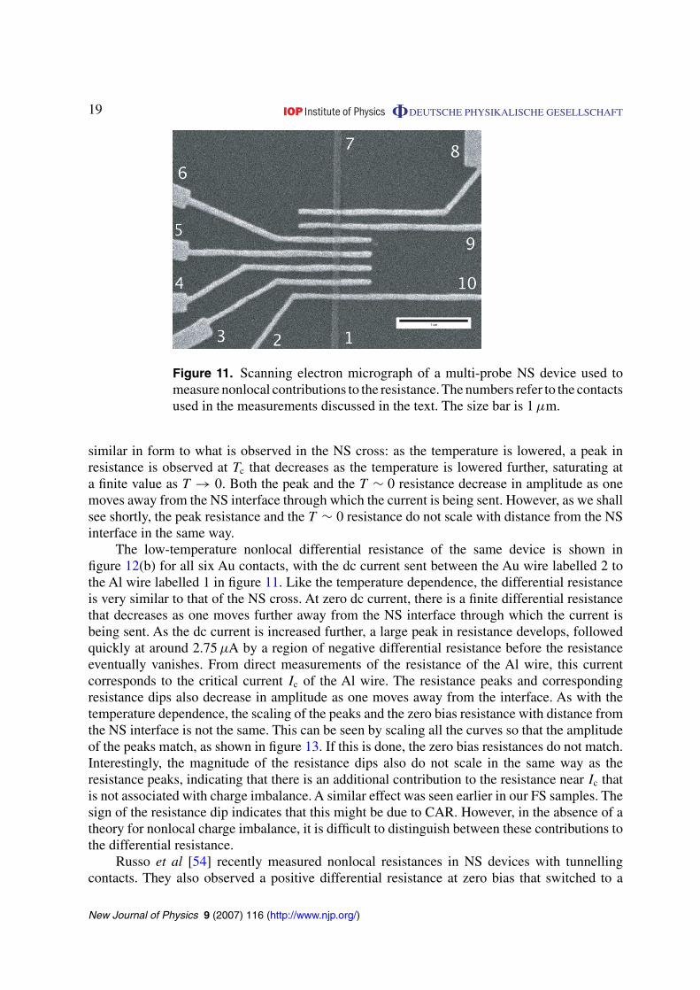
Figure 11. Scanning electron micrograph of a multi-probe NS device used tomeasure nonlocal contributions to the resistance. The numbers refer to the contactsused in the measurements discussed in the text. The size bar is 1 µm.
similar in form to what is observed in the NS cross: as the temperature is lowered, a peak inresistance is observed at Tc that decreases as the temperature is lowered further, saturating ata finite value as T → 0. Both the peak and the T ∼ 0 resistance decrease in amplitude as onemoves away from the NS interface through which the current is being sent. However, as we shallsee shortly, the peak resistance and the T ∼ 0 resistance do not scale with distance from the NSinterface in the same way.
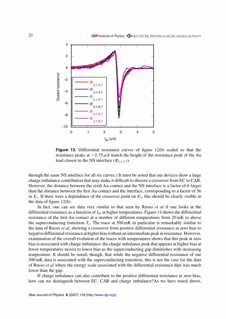
The low-temperature nonlocal differential resistance of the same device is shown infigure 12(b) for all six Au contacts, with the dc current sent between the Au wire labelled 2 tothe Al wire labelled 1 in figure 11. Like the temperature dependence, the differential resistanceis very similar to that of the NS cross. At zero dc current, there is a finite differential resistancethat decreases as one moves further away from the NS interface through which the current isbeing sent. As the dc current is increased further, a large peak in resistance develops, followedquickly at around 2.75 µA by a region of negative differential resistance before the resistanceeventually vanishes. From direct measurements of the resistance of the Al wire, this currentcorresponds to the critical current Ic of the Al wire. The resistance peaks and correspondingresistance dips also decrease in amplitude as one moves away from the interface. As with thetemperature dependence, the scaling of the peaks and the zero bias resistance with distance fromthe NS interface is not the same. This can be seen by scaling all the curves so that the amplitudeof the peaks match, as shown in figure 13. If this is done, the zero bias resistances do not match.Interestingly, the magnitude of the resistance dips also do not scale in the same way as theresistance peaks, indicating that there is an additional contribution to the resistance near Ic thatis not associated with charge imbalance. A similar effect was seen earlier in our FS samples. Thesign of the resistance dip indicates that this might be due to CAR. However, in the absence of atheory for nonlocal charge imbalance, it is difficult to distinguish between these contributions tothe differential resistance.
Russo et al [54] recently measured nonlocal resistances in NS devices with tunnellingcontacts. They also observed a positive differential resistance at zero bias that switched to a
New Journal of Physics 9 (2007) 116 (http://www.njp.org/)
20 DEUTSCHE PHYSIKALISCHE GESELLSCHAFT
Non
loca
l Res
ista
nce
(Ω)
(a)
0
0.2
0.4
0.6
0.8
1
0 0.2
−10
−8
−6
−4
−2
0
2
4
0 1 2 3 4 5
R
R
R
R
R2,1;9,7
R2,1;8,7
Idc (µA)
0.4 0.6 0.8 1
R2,1;3,7
R2,1;4,7
R2,1;5,7
R2,1;6,7
T(K)
2,1;3,7
2,1;4,7
2,1;5,7
2,1;6,7
T=20mK
(b)
Figure 12. (a) Temperature dependence of the zero-bias nonlocal four-terminalresistance involving the fourAu contacts nearest to the NS interface through whichthe current is being sent. The lead numbers refer to figure 11. (b) dc current biasdependence of the nonlocal four-terminal differential resistance involving all sixAu contacts at T = 20 mK. The dc current is sent from the Au lead labelled 2 tothe Al lead labelled 1.
negative differential resistance at finite bias before vanishing entirely as the bias was increasedfurther. They ascribed the zero bias positive differential resistance to EC and the negativedifferential resistance to CAR, with the crossover bias at which the change from positive tonegative current occurred related to the Thouless energy Ec = hD/d2, where d was the thicknessof the superconductor in the experiments. As we noted above, earlier theoretical work indicatedthat in the tunnelling regime, EC and CAR should cancel exactly at all energies, leading toa vanishing nonlocal resistance. However, more recent theoretical work by Morten et al [37]predicts that EC should in fact be dominant for all interface transparencies, and that there alsoshould be a dependence on Ec, although the crossover from positive differential resistance tonegative differential resistance at an energy Ec could not be described.
The data from our sample in figure 12(b) show that the crossover point from positivedifferential resistance to negative differential resistance does not depend on the distance betweenthe NS interface and the second Au contact, since it is the same for all six Au contacts, i.e. thecrossover point does not depend on Ec. (While the data of figure 12(b) is shown as a functionof dc current, the same conclusion is valid as a function of voltage bias, since the current goes
New Journal of Physics 9 (2007) 116 (http://www.njp.org/)
21 DEUTSCHE PHYSIKALISCHE GESELLSCHAFT
−10
−8
−6
−4
−2
0
2
4
0 1 2 3 4
R2,1;3,7
R2,1;4,7
R2,1;5,7
R2,1;6,7
R2,1;9,7
R2,1;8,7
Sca
led
resi
stan
ce
Idc (µA)
5
Figure 13. Differential resistance curves of figure 12(b) scaled so that theresistance peaks at ∼2.75 µA match the height of the resistance peak of the Aulead closest to the NS interface (R2,1;3,7).
through the same NS interface for all six curves.) It must be noted that our devices show a largecharge imbalance contribution that may make it difficult to discern a crossover from EC to CAR.However, the distance between the sixth Au contact and the NS interface is a factor of 6 largerthan the distance between the first Au contact and the interface, corresponding to a factor of 36in Ec. If there were a dependence of the crossover point on Ec, this should be clearly visible inthe data of figure 12(b).
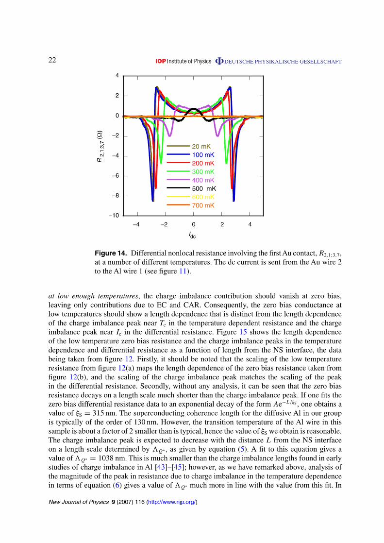
In fact, one can see data very similar to that seen by Russo et al if one looks at thedifferential resistance as a function of Idc at higher temperatures. Figure 14 shows the differentialresistance of the first Au contact at a number of different temperatures from 20 mK to abovethe superconducting transition Tc. The trace at 500 mK in particular is remarkably similar tothe data of Russo et al, showing a crossover from positive differential resistance at zero bias tonegative differential resistance at higher bias without an intermediate peak in resistance. However,examination of the overall evolution of the traces with temperatures shows that this peak at zerobias is associated with charge imbalance: the charge imbalance peak that appears at higher bias atlower temperatures moves to lower bias as the superconducting gap diminishes with increasingtemperature. It should be noted, though, that while the negative differential resistance of our500 mK data is associated with the superconducting transition, this is not the case for the dataof Russo et al where the energy scale associated with the differential resistance dips was muchlower than the gap.
If charge imbalance can also contribute to the positive differential resistance at zero bias,how can we distinguish between EC, CAR and charge imbalance?As we have noted above,
New Journal of Physics 9 (2007) 116 (http://www.njp.org/)
22 DEUTSCHE PHYSIKALISCHE GESELLSCHAFT
−10
−8
−6
−4
−2
0
2
4
−4 −2 0 2 4
20 mK100 mK200 mK300 mK400 mK500 mK600 mK700 mK
R 2
,1;3
,7 (
Ω)
Idc
Figure 14. Differential nonlocal resistance involving the firstAu contact, R2,1;3,7,at a number of different temperatures. The dc current is sent from the Au wire 2to the Al wire 1 (see figure 11).
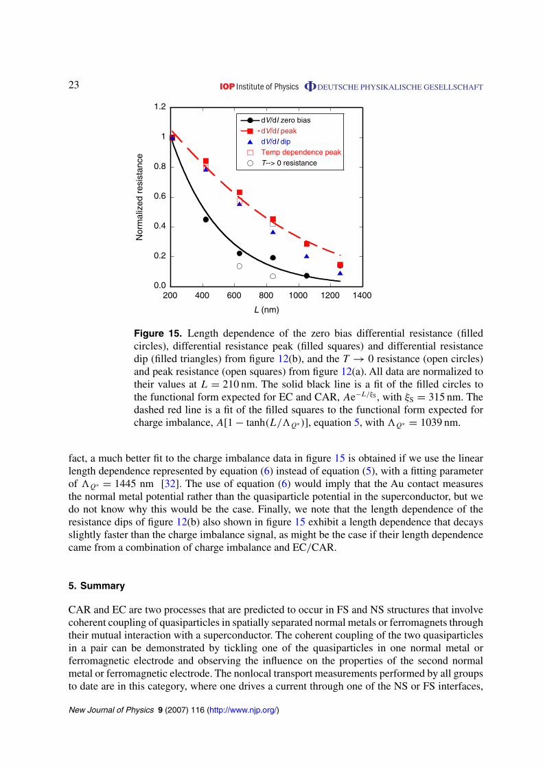
at low enough temperatures, the charge imbalance contribution should vanish at zero bias,leaving only contributions due to EC and CAR. Consequently, the zero bias conductance atlow temperatures should show a length dependence that is distinct from the length dependenceof the charge imbalance peak near Tc in the temperature dependent resistance and the chargeimbalance peak near Ic in the differential resistance. Figure 15 shows the length dependenceof the low temperature zero bias resistance and the charge imbalance peaks in the temperaturedependence and differential resistance as a function of length from the NS interface, the databeing taken from figure 12. Firstly, it should be noted that the scaling of the low temperatureresistance from figure 12(a) maps the length dependence of the zero bias resistance taken fromfigure 12(b), and the scaling of the charge imbalance peak matches the scaling of the peakin the differential resistance. Secondly, without any analysis, it can be seen that the zero biasresistance decays on a length scale much shorter than the charge imbalance peak. If one fits thezero bias differential resistance data to an exponential decay of the form Ae−L/ξS , one obtains avalue of ξS = 315 nm. The superconducting coherence length for the diffusive Al in our groupis typically of the order of 130 nm. However, the transition temperature of the Al wire in thissample is about a factor of 2 smaller than is typical, hence the value of ξS we obtain is reasonable.The charge imbalance peak is expected to decrease with the distance L from the NS interfaceon a length scale determined by Q∗ , as given by equation (5). A fit to this equation gives avalue of Q∗ = 1038 nm. This is much smaller than the charge imbalance lengths found in earlystudies of charge imbalance in Al [43]–[45]; however, as we have remarked above, analysis ofthe magnitude of the peak in resistance due to charge imbalance in the temperature dependencein terms of equation (6) gives a value of Q∗ much more in line with the value from this fit. In
New Journal of Physics 9 (2007) 116 (http://www.njp.org/)
23 DEUTSCHE PHYSIKALISCHE GESELLSCHAFT
0.0
0.2
0.4
0.6
0.8
1
1.2
200 400 600 800 1000 1200 1400
dV/dI zero bias
dV/dI peakdV/dI dipTemp dependence peak
T--> 0 resistance
Nor
mal
ized
res
ista
nce
L (nm)
Figure 15. Length dependence of the zero bias differential resistance (filledcircles), differential resistance peak (filled squares) and differential resistancedip (filled triangles) from figure 12(b), and the T → 0 resistance (open circles)and peak resistance (open squares) from figure 12(a). All data are normalized totheir values at L = 210 nm. The solid black line is a fit of the filled circles tothe functional form expected for EC and CAR, Ae−L/ξS , with ξS = 315 nm. Thedashed red line is a fit of the filled squares to the functional form expected forcharge imbalance, A[1 − tanh(L/Q∗)], equation 5, with Q∗ = 1039 nm.
fact, a much better fit to the charge imbalance data in figure 15 is obtained if we use the linearlength dependence represented by equation (6) instead of equation (5), with a fitting parameterof Q∗ = 1445 nm [32]. The use of equation (6) would imply that the Au contact measuresthe normal metal potential rather than the quasiparticle potential in the superconductor, but wedo not know why this would be the case. Finally, we note that the length dependence of theresistance dips of figure 12(b) also shown in figure 15 exhibit a length dependence that decaysslightly faster than the charge imbalance signal, as might be the case if their length dependencecame from a combination of charge imbalance and EC/CAR.
5. Summary
CAR and EC are two processes that are predicted to occur in FS and NS structures that involvecoherent coupling of quasiparticles in spatially separated normal metals or ferromagnets throughtheir mutual interaction with a superconductor. The coherent coupling of the two quasiparticlesin a pair can be demonstrated by tickling one of the quasiparticles in one normal metal orferromagnetic electrode and observing the influence on the properties of the second normalmetal or ferromagnetic electrode. The nonlocal transport measurements performed by all groupsto date are in this category, where one drives a current through one of the NS or FS interfaces,
New Journal of Physics 9 (2007) 116 (http://www.njp.org/)
24 DEUTSCHE PHYSIKALISCHE GESELLSCHAFT
and measures the resulting nonlocal voltage on the second normal metal or ferromagnet. In theexperiments performed in our group and the work of Beckmann et al and Russo et al, there isstrong evidence for the existence of these nonlocal effects.
A number of issues remain to be resolved. The most critical is the ability to distinguishexperimentally between EC and CAR. Using sample structures that incorporate two ferromagnetsseems to be a very attractive means of distinguishing between EC and CAR, as one needs only toreverse the relative magnetization to switch between EC and CAR. However, as we have seen inour own experiments and those of Beckmann et al, the experimental signal in FSN structures isunexpectedly small, and complications from spin-valve effects and the magnetic fields generatedfrom the ferromagnetic elements cannot be ruled out. In NS structures, the nonlocal effects arelarger and complications from spin-valve effects and local magnetic fields are absent. In FSand NS devices with moderate to good interface transparencies, nonlocal charge imbalance isa prominent effect, and one for which no theoretical description is available. Other means ofdistinguishing between EC and CAR have been proposed such as looking at the correlations inthe current noise between the two NS or FS interfaces [55], but no experimental results have yetbeen published.
In our opinion, it is important to have a theory of EC and CAR that can be used to describethe experimental results. In this regard, the most important aspect is to incorporate the effects ofnonlocal charge imbalance within the same theoretical framework. To our knowledge, this hasnot been done. This would allow us, for example, to fit the experimental current and temperaturedependence of the nonlocal differential resistance which is not possible at present.
Acknowledgments
We thank D Feinberg and D Beckmann for useful discussions. This work was supported by theUS National Science Foundation through grant number DMR-0604601.
References
[1] Pannetier B and Courtois H 2000 J. Low Temp. Phys. 118 599[2] Blonder G E, Tinkham M and Klapwijk T M 1982 Phys. Rev. B 25 4515[3] Zaitsev A V 1984 Sov. Phys.—JETP 59 1015[4] Nguyen C, Kroemer H and Hu E L 1992 Phys. Rev. Lett. 69 2847[5] Nitta J, Akazaki T and Takayanagi H 1994 Phys. Rev. B 49 3659[6] de Vegvar P G N, Fulton T A, Mallison W H and Miller R E 1994 Phys. Rev. Lett. 73 1416[7] Pothier H, Gueron S, Esteve D and Devoret M H 1994 Phys. Rev. Lett. 73 2488[8] Takayanagi H, Hansen J B and Nitta J 1995 Phys. Rev. Lett. 74 162[9] Courtois H, Gandit Ph, Mailly D and Pannetier B 1996 Phys. Rev. Lett. 76 130
[10] Antonov V N, Volkov A F and Takayanagi H 1997 Phys. Rev. B 55 3836[11] Hoss T, Strunk C, Nussbaumer T, Huber R, Staufer U and Schönenberger C 2000 Phys. Rev. B 62 4079[12] Reulet B, Kozhevnikov A A, Prober D E, Belzig W and Nazarov Yu V 2003 Phys. Rev. Lett. 90 66601[13] Lefloch F, Hoffman C, Sanquer M and Quirion D 2003 Phys. Rev. Lett. 90 67002[14] Andreev A F 1964 Zh. Eksp. Teor. Fiz. 46 1823
Andreev A F 1964 Sov. Phys.—JETP 19 1228 (Engl. Transl.)[15] Buzdin A I 2005 Rev. Mod. Phys. 77 935[16] de Jong M J M and Beenakker C W J 1995 Phys. Rev. Lett. 74 1657[17] Kashiwaya S, Tanaka Y, Yoshida N and Beasley M R 1999 Phys. Rev. B 60 3572
New Journal of Physics 9 (2007) 116 (http://www.njp.org/)
25 DEUTSCHE PHYSIKALISCHE GESELLSCHAFT
[18] Zutic I and Valls O T 1999 Phys. Rev. B 60 6320[19] Dimoulas A 2000 Phys. Rev. B 61 9729[20] Melin R 2000 Europhys. Lett. 51 202[21] Upadhyay S K, Palanisami A, Louie R N and Buhrman R A 1998 Phys. Rev. Lett. 81 3247[22] Soulen R J et al 1998 Science 282 85[23] Mazin I I, Golubov A A and Nadgorny B 2001 J. Appl. Phys. 89 7576[24] Lawrence M D and Giordano N 1999 J. Phys.: Condens. Matter 11 1089[25] Petrashov V T, Sosnin I A, Cox I, Parsons A and Troadec C 1999 Phys. Rev. Lett. 83 3281[26] Ryazanov V V, Oboznov V A, Rusanov A Yu, Veretennikov A V, Golubov A A and Aarts J 2001 Phys. Rev.
Lett. 86 2427[27] Kontos T, Aprili M, Lesueur J, Genet F, Stephanidis B and Boursier R 2002 Phys. Rev. Lett. 89 137007[28] Robinson J W A, Piano S, Burnell G, Bell C and Blamire M G 2006 Phys. Rev. Lett. 97 177003[29] Keizer R S, Goennenwein S T B, Klapwijk T M, Miao G, Xiao G and Gupta A 2006 Nature 439 825[30] Sosnin I, Cho H, Petrashov V T and Volkov A F 2006 Phys. Rev. Lett. 96 157002[31] Byers J M and Flatte M E 1995 Phys. Rev. Lett. 74 306[32] Cadden-Zimansky P and Chandrasekhar V 2006 Preprint cond-mat/0609749[33] Falci G, Feinberg D and Hekking F W J 2001 Europhys. Lett. 54 255[34] Melin R and Feinberg D 2002 Eur. Phys. J. B 26 101[35] Feinberg D 2003 Eur. Phys. J. B 36 419[36] Melin R and Feinberg D 2004 Phys. Rev. B 70 174509[37] Morten J P, Brataas A and Belzig W 2006 Preprint cond-mat/0606561[38] Clarke J 1972 Phys. Rev. Lett. 28 1363[39] Tinkham M and Clarke J 1972 Phys. Rev. Lett. 28 1366[40] Schmid A and Schon G 1975 J. Low Temp. Phys. 20 207[41] Chi C C and Clarke J 1979 Phys. Rev. B 19 4495[42] Stuivinga M, Mooij J E and Klapwijk T M 1981 Physica 108B + C 1023[43] Mamin H J, Clarke J and Van Harlingen D J 1984 Phys. Rev. B 29 3881[44] Chien C-J and Chandrasekhar V 1999 Phys. Rev. B 60 3655[45] Park M, Isaacson M S and Parpia J M 1995 Phys. Rev. Lett. 75 3740[46] Park M, Isaacson M S and Parpia J M 1997 Phys. Rev. B 55 9067[47] Aumentado J and Chandrasekhar V 1999 Appl. Phys. Lett. 74 1898[48] Eom J 1998 Doctoral Thesis Northwestern University[49] Jiang Z, Aumentado J, Belzig W and Chandrasekhar V 2003 Theory of Quantum Transport in Metallic and
Hybrid Nanostructures ed A Glatz, V I Kozub and V M Vinokur (Dordrecht: Kluwer) p 57[50] Johnson M and Silsbee R H 1985 Phys. Rev. Lett. 55 1790[51] Jedema F J, Filip A T and van Wees B J 2001 Nature 410 345[52] Ji Y, Hoffmann A, Jiang J S and Bader S D 2004 Appl. Phys. Lett. 85 6218[53] Beckmann D, Weber H B and Löhneysen H V 2004 Phys. Rev. Lett. 93 197003[54] Russo S, Kroug M, Klapwijk T M and Morpurgo A F 2005 Phys. Rev. Lett. 95 027002[55] Bignon G, Houzet M, Pistolesi F and Hekking F W J 2004 Europhys. Lett. 67 110
New Journal of Physics 9 (2007) 116 (http://www.njp.org/)


![Andreev Reflections and transport phenomena in ...€¦ · Andreev re°ections [S2,S8]. The point contact Andreev re°ection spectroscopy carried out on RuSr2GdCu2O8 has evidenced](https://static.fdocuments.in/doc/165x107/6060572c65c18a52267c888c/andreev-reflections-and-transport-phenomena-in-andreev-reections-s2s8.jpg)