Charge and Energy Transfer in Different Types of Two ...
152
Charge and Energy Transfer in Different Types of Two-Dimensional Heterostructures By Matthew Z. Bellus Submitted to the graduate degree program in Department of Physics and Astronomy and the Graduate Faculty of the University of Kansas in partial fulfillment of the requirements for the degree of Doctor of Philosophy. Committee members Dr. Hui Zhao, Chairperson Dr. Judy Wu Dr. Siyuan Han Dr. Wai-Lun Chan Dr. Rongqing Hui Date defended: March 02, 2018
Transcript of Charge and Energy Transfer in Different Types of Two ...

Charge and Energy Transfer in Different Types ofTwo-Dimensional Heterostructures
By
Matthew Z. Bellus
Submitted to the graduate degree program in Department of Physics and Astronomy and theGraduate Faculty of the University of Kansas in partial fulfillment of the requirements for the
degree of Doctor of Philosophy.
Committee members
Dr. Hui Zhao, Chairperson
Dr. Judy Wu
Dr. Siyuan Han
Dr. Wai-Lun Chan
Dr. Rongqing Hui
Date defended: March 02, 2018

The Thesis Committee for Matthew Z. Bellus certifiesthat this is the approved version of the following thesis :
Charge and Energy Transfer in Different Types of Two-Dimensional Heterostructures
Dr. Hui Zhao, Chairperson
Date approved: May 02, 2018
ii

Abstract
In the last decade or so, layered materials have attracted significant attention due to
their promise for tailoring electronic properties at an atomic level. Individually, these
materials have exhibited strong attributes, relevant for both electronic and optoelec-
tronic applications. However, the real world implementation of semiconducting mate-
rials is often derived from the junctions they form with other semiconductors. Thus,
much of the interest in 2D materials arises from exploiting their ability to form low
dimensional heterostructures. From a structural stand point, there are two ways these
heterostructures can be formed, either vertically or laterally. The more common, ver-
tical heterostructures, are intriguing due to their van der Waals adhesion, which elimi-
nates many of the constraints attributed to lattice matching between materials. Lateral
heterostructures, on the other hand, provide the unique opportunity to form in-plane
junctions within a 2D sheet, creating novel 1D interfaces.
To better understand these various heterostructures, this dissertation aims to explore
photocarrier dynamics, using ultrafast laser spectroscopy techniques, in several types
of structures yet to be extensively studied. First, charge and energy transfer mecha-
nisms in vertical heterostructures formed between various transition metal dichalco-
genide monolayers are studied, highlighting the addition of type-I band alignment to
the discussion. Next, the extent to which materials can interact electronically through
van der Waals adhesion is explored at the interface between amorphous and crystalline
layers.
From there, the focus shifts slightly to carrier dynamics across lateral junctions formed
within monolayer sheets of transition metal dichalcogenides. This includes a discus-
iii

sion on lateral heterostructures, formed between different materials, as well as ho-
mostructures where an electronic junction can be induced in a single material. All of
these studies will provide a unique overview on the possible directions and applica-
tions for which two dimensional materials can be facilitated.
This dissertation includes previously published authored material.
iv

Acknowledgements
I am truly grateful for the experiences and knowledge I have gained in my time at The
University of Kansas. I have had the opportunity to meet incredible people along this
journey and would like to take this section to thank those whom have gotten me to
this milestone in life. I have been very fortunate in my graduate experience to work
with two amazing advisors, Dr. Hsin-Ying Chiu and Dr. Hui Zhao. First, I would
sincerely like to thank Dr. Chiu, who initially welcomed me into her group during my
final year of undergrad. Her passion for science and discovery, and belief in me, truly
inspired me to continue my journey in physics and pursue my PhD. I have learned so
much from her and been provided so many opportunities for which I will be forever
grateful. Next, I need to thank Dr. Zhao, who graciously accepted me into his research
group part way through my graduate education. His patience and understanding as
I adjusted to a new group and shifted my research focus is much appreciated. The
opportunities he has provided through sending me to conferences and events outside
of KU, as well as the vision and guidance he provided on so many research projects
has been amazing. So much of the positive direction in which I believe my life to be
headed is owed to these two.
I also need to thank my fellow lab mates, especially Dr. Frank Ceballos and Dr. Quin-
nan Cui, who helped teach me the majority of experimental techniques and lab prac-
tices. I would like to thank them along with Samuel Lane and Peymon Zereshki for
their intellectual inputs and emotional support throughout this process, as well. The
friendships I have built within the lab are ones I hope last a lifetime.
I also want to thank the other members of my committee, Dr. Judy Wu, Dr. Siyuan
v

Han, Dr. Wai-Lun Chan, and Dr. Rongqing Hui. I have been fortunate to learn from
each of them in both the classroom and from their insightful inputs on research. Their
experience and guidance has helped mold me into the scientist I am today. I need to
give a special thanks to Dr. Wu and her group for allowing me to learn about and
utilize various research tools from her lab.
I need to thank the various collaborators that have provided both samples, theory, and
input for projects contained within this dissertation. Dr. Xiao Cheng Zeng and re-
searchers, at the University of Nebraska-Lincoln, provided the theory on TMD band
alignment leading to the work on type-I heterostructures. Dr. Shu Ping Lau and his
group from The Hong Kong Polytechnic University provided us with the amorphous
black phosphorus samples. Finally, I need to thank Dr. Kai Xiao and team at Oak
Ridge National Laboratory for providing the lateral heterostructure samples. It is
through collaborations like these that scientific research truly flourishes.
Last, but certainly not least, I would like to acknowledge all my friends and family
that have given me so much support over the years. My parents, Peter and Jeanne,
have furnished me with as good an upbringing as anyone could ask for. I could never
have gotten to this point in my life without their unconditional love and support. I also
thank my brother Alex and his wife Molly for their encouragement along the way and
for being such great role models for how to pursue the next chapter in my life.
vi

Contents
1 Introduction 1
1.1 Two-Dimensional Materials . . . . . . . . . . . . . . . . . . . . . . . . . . . . . 1
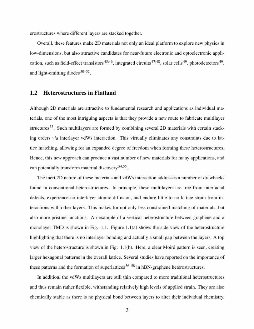
1.2 Heterostructures in Flatland . . . . . . . . . . . . . . . . . . . . . . . . . . . . . . 3
1.3 Charge and energy transfer in van der Waals multilayers . . . . . . . . . . . . . . 7
1.4 Overview of Dissertation . . . . . . . . . . . . . . . . . . . . . . . . . . . . . . . 10
2 Experimental Techniques 12
2.1 Photoluminescence Spectroscopy . . . . . . . . . . . . . . . . . . . . . . . . . . . 12
2.2 Time Resolved Pump-Probe Spectroscopy . . . . . . . . . . . . . . . . . . . . . . 14
2.3 Spatiotemporally Resolved Pump-Probe Spectroscopy . . . . . . . . . . . . . . . 17
2.3.1 Photocarrier Diffusion . . . . . . . . . . . . . . . . . . . . . . . . . . . . 19
2.3.2 Photocarrier Drift . . . . . . . . . . . . . . . . . . . . . . . . . . . . . . . 21
3 Vertical Heterostructures Formed by Monolayer TMDs 23
3.1 Trion Formation in Type-II MoSe2-WS2 vdWs Heterostructure . . . . . . . . . . . 23
3.1.1 Sample Fabrication and Characterization . . . . . . . . . . . . . . . . . . 24
3.1.2 Results and Discussion . . . . . . . . . . . . . . . . . . . . . . . . . . . . 24
3.2 Exciton Transfer in Type-I vdW Heterostructures . . . . . . . . . . . . . . . . . . 30
3.2.1 2H-2H MoTe2-WSe2 . . . . . . . . . . . . . . . . . . . . . . . . . . . . . 30
3.2.2 2H-Distorted 1T MoS2-ReS2 . . . . . . . . . . . . . . . . . . . . . . . . . 37
3.3 Summary . . . . . . . . . . . . . . . . . . . . . . . . . . . . . . . . . . . . . . . 46
4 2D Amorphous-Crystalline Semiconducting Heterostructures 47
4.1 Introduction to Amorphous Semiconductors . . . . . . . . . . . . . . . . . . . . . 48
vii

4.2 Carrier Dynamics in Amorphous Black Phosphorus Thin Films . . . . . . . . . . . 50
4.2.1 Fabrication and Characterization of aBP thin Films . . . . . . . . . . . . . 50
4.2.2 Results and Discussion . . . . . . . . . . . . . . . . . . . . . . . . . . . . 52
4.3 Carrier Transfer in 2D WS2-aBP Vertical Heterostructure . . . . . . . . . . . . . . 59
5 Exciton Dynamics in 2D Lateral Heterostructures 70
5.1 Introduction to 2D Lateral Heterostructures . . . . . . . . . . . . . . . . . . . . . 70
5.2 Photocarrier Drift Across Type-I MoS2-MoSe2 Lateral Heterostructure . . . . . . . 71
5.2.1 Exciton Dynamics in MoSe2 and MoS2 . . . . . . . . . . . . . . . . . . . 73
5.2.2 Observation of Type-I Band Alignment . . . . . . . . . . . . . . . . . . . 75
5.2.3 Observation of Exciton Drift . . . . . . . . . . . . . . . . . . . . . . . . . 76
5.2.4 Model of Carrier Dynamics . . . . . . . . . . . . . . . . . . . . . . . . . 82
6 Lateral Homostructures Formed in Monolayer TMDs 89
6.1 Introduction to TMD Lateral Homostructures . . . . . . . . . . . . . . . . . . . . 89
6.2 Junction Formation in MoSe2 Monolayer by Increased Coulomb Screening . . . . 90
6.2.1 Spatiotemporally Resolved Carrier Distributions in MoSe2 and hBN Cov-
ered MoSe2 . . . . . . . . . . . . . . . . . . . . . . . . . . . . . . . . . . 93
6.2.2 Exciton Drift at the Lateral Junction Between Uncovered and Covered MoSe2 95
6.3 Summary . . . . . . . . . . . . . . . . . . . . . . . . . . . . . . . . . . . . . . . 100
7 Summary and Outlook 101
Appendix A Fabrication and Characterization of vdWs Heterostructures 104
A.1 Mechanical Exfoliation and vdWs Stacking . . . . . . . . . . . . . . . . . . . . . 104
A.2 Optical Contrast Methods . . . . . . . . . . . . . . . . . . . . . . . . . . . . . . . 106
A.3 Other Characterization Methods . . . . . . . . . . . . . . . . . . . . . . . . . . . 107
viii

List of Figures
1.1 Schematic of a TMD-Graphene vertical heterostructure. (a) Side view of the het-
erostructure. (b) Top view of the heterostructure showing the overlap of the hon-
eycomb hexagonal lattices of the two materials. . . . . . . . . . . . . . . . . . . . 4
1.2 Number of publications by year according to the Web of Science on the topics
of "Two-Dimensional" and "Heterostructures" (Red). The blue and yellow data
represents the number of publications within the realm of 2D heterostructures for
transition metal dichalcogenides and graphene, respectively. . . . . . . . . . . . . 5
1.3 Schematic of a TMD-TMD lateral heterostructure. (a) Side view of the heterostruc-
ture. (b) Top view of the heterostructure. . . . . . . . . . . . . . . . . . . . . . . 7
1.4 The three types of band alignment that dictate charge transfer in semiconducting
heterostructures. (a) Type-I band alignment, where the CMB and VBM are both on
the same side of the junction causing both carrier to transfer in the same direction.
(b) Type-II alignment where the CBM and VBM are located on different sides
causing charge separation. (c) Type-III alignment where the CBM of one material
is below the VBM of the other. This often results in tunneling mechanisms across
the junction. . . . . . . . . . . . . . . . . . . . . . . . . . . . . . . . . . . . . . . 8
1.5 Types of energy transfer across semiconducting junctions. (a) Example of a Förster-
type energy transfer process. The pink arrows represent the recombination process
in one layer that leads to the excitation in the other (b) Example of a Dexter-type
energy transfer process. Here, electrons and holes can move across the junction as
a bound pair. . . . . . . . . . . . . . . . . . . . . . . . . . . . . . . . . . . . . . 9
ix

2.1 Energy and momentum transitions for photoexcited carriers for (a) direct gap and
(b) indirect gap materials. The curved arrows represent photons, either excitation
photons (blue) or emitted photons (red). The more squiggly arrows (yellow) repre-
sent phonons which assist in momentum transition in materials with indirect band
gaps. . . . . . . . . . . . . . . . . . . . . . . . . . . . . . . . . . . . . . . . . . . 13
2.2 Schematic of a typical PL experimental setup. . . . . . . . . . . . . . . . . . . . 14
2.3 Schematic of the mechanism behind time resolved pump-probe experiments. Red
arrows represent the probe photons and green arrows the pump photons. The blue
and red circles represent electrons and holes, respectively (a) Early delay times,
before the pump reaches the samples. Probe photons are mostly absorbed by the
material in the form of excited electrons. The red dashed arrows represents these
excitations. (b) The system just after the pump reaches the sample. The electrons
are excited to the conduction band (green dashed arrows). With no available states
near the band edge, the probe is mostly reflected. (c) Later delay times where the
electron-hole pairs recombine, freeing up states in the conduction band allowing
for some probe photons to be absorbed. . . . . . . . . . . . . . . . . . . . . . . . 15
2.4 Setup for time resolved pump-probe spectroscopy. (a) Schematic of the process to
create the ultrafast pump and probe beams. (b) Schematic of the overall experi-
mental setup. . . . . . . . . . . . . . . . . . . . . . . . . . . . . . . . . . . . . . 16
2.5 (a) Schematic of the how the carrier distribution is resolved spatially. (b) Sample
spatial profiles of the differential reflection based on this measurement technique.
The blue, purple, and red curves represent the expected evolution of these profiles
for later delay times (t1 > t2 > t3). The width of the distribution is expected to
increase over time as carriers diffuse outward. . . . . . . . . . . . . . . . . . . . 18
x

2.6 Expected spatial profiles for a carrier distribution undergoing different drift trans-
port processes. (a) An applied electric field causes charge separation. The dis-
tribution will then split with two peaks representing their respective carriers. (b)
Exciton drift causes the whole distribution to move in one direction. . . . . . . . . 22
3.1 Optical images of the MoSe2-WS2 heterostructure sample at different steps of fab-
rication. (a,b) Images of the MoSe2 and WS2 monolayer samples on the PDMS
substrates. (c) Image of the MoS2 sample after being transferred to a Si/SiO2 sub-
strate. (d) Image of the heterostructure after the transfer of the WS2 sample. The
scale bars are 20 µm. Reproduced with permission from ACS Nano 2015 9 (6),
6459-6464. Copyright 2015 American Chemical Society. . . . . . . . . . . . . . . 25
3.2 Photoluminescnece spectra measured from WS2 (blue), MoSe2 (red), and the het-
erostructure (black). Reproduced with permission from ACS Nano 2015 9 (6),
6459-6464. Copyright 2015 American Chemical Society. . . . . . . . . . . . . . . 26
3.3 Expected band alignment of the MoSe2-WS2 heterostructure. Electrons in MoSe2
transfer to WS2 creating bound trions. The resulting recombination of these parti-
cle clusters results in a shifted peak in the PL. Reproduced with permission from
ACS Nano 2015 9 (6), 6459-6464. Copyright 2015 American Chemical Society. . . 27
3.4 Photoluminescence spectra measured from the heterostructure for different pump
excitation powers. The red and blue curves are Gaussian fits to the exciton and trion
peaks respectively. The orange curve is the cumulative fit from the two Gaussian
functions. Reproduced with permission from ACS Nano 2015 9 (6), 6459-6464.
Copyright 2015 American Chemical Society. . . . . . . . . . . . . . . . . . . . . 28
xi

3.5 Power dependent trends from 3.4 (a,b) The peak energy measured from the exciton
and trion peaks as a function of the excitation power. (c) The difference between (a)
and (b). (d,e) The height of the exciton and trion peaks as a function of excitation
power. (f) The ratio of the peak heights found in (d) and (e). Reproduced with
permission from ACS Nano 2015 9 (6), 6459-6464. Copyright 2015 American
Chemical Society. . . . . . . . . . . . . . . . . . . . . . . . . . . . . . . . . . . . 29
3.6 (a) Optical image of the MoTe2-WSe2 heterostructure sample. (b) Calculated band
alignment between MLs of WSe2 and MoTe2. The orange and gray circles repre-
sent excited electrons and holes, respectively, which are expected to transfer to the
MoTe2 layer. . . . . . . . . . . . . . . . . . . . . . . . . . . . . . . . . . . . . . 31
3.7 Photoluminescence spectroscopy data measured from WSe2 (blue), MoTe2 (red),
and the heterostructure (black). . . . . . . . . . . . . . . . . . . . . . . . . . . . . 32
3.8 Differential reflection measurements using a 1.31 eV probe pulse and a 1.65 eV
pump pulse. The blue squares were measured from the heterostructure and show a
significantly higher signal than that measured from the isolated MoTe2 ML (Grey
Squares). The purple and red lines represent double exponential fits to the het-
erostructure and ML MoTe2 data respectively. The yellow squares represent mea-
surements on the heterostructure with the pump and probe switched, 1.65 eV probe
and 1.31 eV pump. This is to probe carriers excited in MoTe2 that might transfer
to WSe2. . . . . . . . . . . . . . . . . . . . . . . . . . . . . . . . . . . . . . . . . 34
3.9 Pump energy dependence on the differential reflection of 1.31 eV probe measuring
the heterostructure. The inset shows the peak differential reflection signal for the
different pump energies. . . . . . . . . . . . . . . . . . . . . . . . . . . . . . . . 36
3.10 Short and long scale differential reflection measurements on WSe2 ML (Blue) and
the heterostructure (Red) using a 1.65 eV probe and 2.1 eV pump. . . . . . . . . . 37
xii

3.11 (a) Calculated band alignment of monolayer MoS2 and ReS2. (b) Calculated band
structure of the MoS2-ReS2 heterosturcture. The red and green symbols represent
contribution from MoS2 and ReS2, respectively. Reproduced from Ref. 135 with
permission from The Royal Chemical Society. . . . . . . . . . . . . . . . . . . . . 38
3.12 (a) Optical image of the MoS2-ReS2 sample. (b) Contrast measured from the green
color channel along the yellow line in (a). (c) Raman spectra measured from MoS2
(red) and ReS2 (green) The large peak at a Raman shift of around 520 cm−1 is
from the silicon substrate. Reproduced from Ref. 135 with permission from The
Royal Chemical Society. . . . . . . . . . . . . . . . . . . . . . . . . . . . . . . . 39
3.13 Differential reflection of a 1.53 eV probe measured from ML ReS2 (open symbols)
and the MoS2-Res2 heterostructure (closed symbols) for different pump energies,
1.57 eV (red symbols) and 1.85 eV (green symbols). Reproduced from Ref. 135
with permission from The Royal Chemical Society. . . . . . . . . . . . . . . . . . 42
3.14 Differential reflection of a 1.85 eV probe as a function of probe delay. The black
squares represent the measurements from ML MoS2 using a 3.06 eV pump. The
white squares represent the measurements from the heterostructure using a 1.53
eV pump to excite carriers only in the ReS2 layer. Reproduced from Ref. 135 with
permission from The Royal Chemical Society. . . . . . . . . . . . . . . . . . . . . 43
3.15 Normalized, time-dependent differential reflection signals on a short time scale to
show the transfer dynamics. The green squares are measured using a 1.53 eV probe
and 1.85 eV pump in ML ReS2 (open) and the heterostructure (closed). The blue
squares are measured from ML MoS2 using a 1.85 eV probe and 3.06 eV pump.
The lines represent fits to the measured data. The green line is fit to eq. 3.1 and
the blue is exponential decay fit. Reproduced from Ref. 135 with permission from
The Royal Chemical Society. . . . . . . . . . . . . . . . . . . . . . . . . . . . . 45
4.1 Top and side view of the lattice structure of (a) crystalline and (b) amorphous black
phosphorus. . . . . . . . . . . . . . . . . . . . . . . . . . . . . . . . . . . . . . . 48
xiii

4.2 Structural characterization and optical properties of the a-BP thin films. (a) EDX
spectrum of the aBP thin films, confirming that pure phosphorus films were ob-
tained. (b) High-resolution TEM image of the 10-nm a-BP film, combining the
SAED pattern shown inset, revealing the highly disordered feature of the obtained
films. (c) XRD pattern of the a-BP film grown on SiO2/Si substrate. The only
emerged peak is Si (400), further confirming the amorphous nature of the BP film.
(d) Raman spectra of the aBP thin films with different thicknesses. (e) PL spectrum
of the 2 nm aBP film under the excitation of an 808 nm laser. c©IOP Publishing.
Reproduced with permission. All rights reserved. . . . . . . . . . . . . . . . . . . 51
4.3 Differential reflection of then 2 nm aBP ultrathin film. (a) Schematics of pump
and probe scheme with respect to the electronic bands of the 2 nm aBP film. (b)
Differential reflection of the 2 nm aBP film for different values of pump fluence.
(c) Same as (b), but on a larger time range and in semi-logarithm scale (d) Peak
∆R/R0 signal as a function of pump fluence. The solid line shows a fit to a standard
saturation model. (e) The decay times, t1 (black) and t2 (red), obtained from from
double exponential fits of the data in (c) as a function of pump fluence. c©IOP
Publishing. Reproduced with permission. All rights reserved. . . . . . . . . . . . . 53
4.4 Exciton diffusion in the 2 nm aBP ultrathin film measured by spatially resolved
differential reflection. (a) Spatiotemporal differential reflection signal. (b) Spatial
Gaussian profiles for different delay times. (c) The squared width of the Gaussian
profiles as a function of the probe delay. The data is fit with a linear function
in order to extract the diffusion coefficient from the slope. c©IOP Publishing.
Reproduced with permission. All rights reserved. . . . . . . . . . . . . . . . . . . 56
xiv

4.5 Differential reflection and exciton diffusion in the 5 and 10 nm aBP ultrathin films
(a) Differential reflection of the 2, 5, and 10 nm aBP thin films plotted on a log
scale vs relative probe delay. (b) Spatiotemporal differential reflection signal of the
5 nm aBP film (c) Spatiotemporal differential reflection signal of the 10 nm aBP
film (d) The squared width of the Gaussian profiles as a function of the probe delay
for the 2, 5, and 10 nm aBP films. Each dataset is fit with a linear function in order
to extract the diffusion coefficient from the slope. c©IOP Publishing. Reproduced
with permission. All rights reserved. . . . . . . . . . . . . . . . . . . . . . . . . . 58
4.6 (a,b) Optical images of the samples used in this study. ML WS2 is outlined by blue
and hBN by white. (a) Optical image of the sample with bulk hBN. (b) Optical
image of the sample using few layer hBN. (c) Photoluminescence spectroscopy
results of ML WS2 on bulk hBN (red), few layer hBN (blue), and directly on aBP
(black). The inset shows the normalized PL. . . . . . . . . . . . . . . . . . . . . . 61
4.7 Estimated band alignment and expected charge transfer of the WS2 and aBP het-
erostructure based on the calculated CBM and VBM values from literature. The
fairly large valence band offset results in hole transfer from WS2 to aBP, whereas
with a small conduction band offset and relative uncertainty of the true alignment
of aBP, the direction of electron transfer is less certain. From this, we would expect
the band alignment to be either type-I or type-II. . . . . . . . . . . . . . . . . . . 62
4.8 Power dependent PL spectroscopy results of ML WS2 on few layer hBN. The
colored lines are triple Lorentzian fits to the data. The blue lines are the main the
A-exciton peak,the green lines are the secondary peak, and the red lines are the
third peak. The yellow lines represent the cumulative fit. . . . . . . . . . . . . . . 64
4.9 Power dependent trends from the Lorentz fits in Fig. 4.8. These are the (a) emis-
sion energy, (b) peak height, (c) FWHM, and (d) integrated PL intensity of the
neutral exciton (blue), trion (green), and biexciton (red). All fit lines are linear fits
to these trends. . . . . . . . . . . . . . . . . . . . . . . . . . . . . . . . . . . . . 65
xv

4.10 Time dependent differential reflection measurements of a 2.0 eV probe. (a) Log
scale with measurements of aBP alone (grey), WS2 on aBP (blue), and WS2 on
bulk hBN (red). (b) Same measurements as in (a) but normalized to more dramat-
ically show the difference in decay features. . . . . . . . . . . . . . . . . . . . . . 66
4.11 Normalized time dependent differential reflection measurements of a 2.0 eV probe
on a short, few ps time scale. The blue line represents a Gaussian integral with a
FWHM of 0.43 ps. The red line is a transfer model following the equation in the
legend. . . . . . . . . . . . . . . . . . . . . . . . . . . . . . . . . . . . . . . . . 67
4.12 Differential reflection of a 0.8 eV probe from aBP (red) and WS2 on aBP (blue),
injecting carriers only in aBP with a 1.55 eV pump. . . . . . . . . . . . . . . . . . 68
5.1 (a) Schematic of the crystal structure for an ideal MoS2-MoSe2 heterostructure.
(b) Optical image of the sample with alternating 7 µm strips of MoS2 and MoSe2.
Tge bluish colored region is the MoSe2 covered by a SiO2 film. (c) Schematic of
the band alignment of the sample and the pump-probe experiment. The blue and
red arrows represent the pump and probe energies, respectively. A probe resonant
with the gap energy in MoSe2 will not be sensitive to carriers in MoS2 (d) Peak
differential reflection scanned across the 7 µm sample shown in (b). The yellow
arrow in (b) shows the path of the scan. . . . . . . . . . . . . . . . . . . . . . . . 72
5.2 (a) Time resolved differential reflection signal measured in different regions of the
sample. The blue and gray squares represent the signal from a 1.53 eV probe,
resonant with MoSe2, measured from MoSe2 and MoS2, respectively. The black
lines represent bi-exponential fits to the data. (b) The same measurements as in
(a), but on a shorter (few ps) time scale. . . . . . . . . . . . . . . . . . . . . . . . 74
xvi

5.3 (a) Optical image of the sample with 0.5 µm alternating strips of MoS2 and MoSe2.
(b) Time resolved differential reflection of a 1.53 eV probe for isolated MoSe2
(blue) and the 500 nm strips (orange). The black curves represent exponential fits
to the data. (c) Short time scale measurements of the same regions in (b). The
gray line represents a Gaussian integral fit to the rise time of the isolated MoSe2
data and the red line is a transfer model for the rise time of the signal from the
heterostructure. . . . . . . . . . . . . . . . . . . . . . . . . . . . . . . . . . . . . 76
5.4 (a) Schematic of the expected band alignment and exciton transport. The blue and
red arrows represent the energy of the pump and probe, respectively. (b) Schematic
of the differential reflection scheme near the junction at the time of carrier injec-
tion. The yellow and red circles are excitons injected in MoS2 and MoSe2, re-
spectively. The black line represents the measured center of the distribution (c)
Schematic of the experiment at a later time, after carrier injection. The measured
center of the profile (black line) shifts towards the junction as excitons transfer
from MoS2. . . . . . . . . . . . . . . . . . . . . . . . . . . . . . . . . . . . . . . 78
5.5 (a) Spatiotemporal differential reflection measurements measured across a single
MoS2-MoSe2 junction. The red line shows the peak signal in time. The vertical
white line, at x = 0, represents the junction between materials. (b) Spatial profiles
of the differential reflection measurements for different delay times with the colors
going from violet to red representing early to late delay times. The color coordi-
nated lines are asymmetric double sigmoidal fits to the data. (c) A sampling of
normalized spatial profiles with the same fits from (b) providing a better visual of
the shifting profile. (d) The position of the peak center of each fit as a function of
delay time. . . . . . . . . . . . . . . . . . . . . . . . . . . . . . . . . . . . . . . . 79
5.6 Width of the left (red) and right (blue) contributions to the asymmetric double
sigmoidal fits to the spatial profiles. . . . . . . . . . . . . . . . . . . . . . . . . . 80
xvii

5.7 (a) Spatiotemporal differential reflection of a 1.53 eV probe for a pump energy of
1.72 eV. (b) The spatial profiles at a sample of delay time. The fits in this case are
Gaussian fits. (c) Plot of the Gaussian center of each spatial profile fit as a function
of the delay time. . . . . . . . . . . . . . . . . . . . . . . . . . . . . . . . . . . . 81
5.8 Depiction of how the spatial convolution is found in the simulation of the pump-
probe experiment. The red curve represents the probe sensitivity profile. The teal
curves are the injected carrier density profiles for different sample positions. The
black curve is the convolution of the two at time, t=0. . . . . . . . . . . . . . . . . 84
5.9 (a) Simulation of the spatiotemporal transient absorption experiment without the
inclusion of carrier transfer. (b) Peak position as a function of probe delay as
calculated by the model (red) and from the data (blue). . . . . . . . . . . . . . . . 85
5.10 Injected carrier density profile centered at the junction for different probe delays.
For simplicity, the displacement parameter, here, is varied linearly in time at a rate
of 8×105 cm/s. . . . . . . . . . . . . . . . . . . . . . . . . . . . . . . . . . . . . 87
5.11 (a) Peak position extracted from the measured data (black squares) and the model
(red line) as a function of probe delay. The model uses a value of 0.01 µm/ps for
the velocity parameter. (b) Contour plot of the modeled carrier density as function
of sample position and probe delay. This is for a single injection site (pump spot
position), centered a little more than 0.5 µm into MoSe2, to show how the transfer
and build up functions effect the distribution. . . . . . . . . . . . . . . . . . . . . 88
6.1 (a) Optical image of one of the samples used in this experiment. (b) Photolumi-
nescence measurements for ML MoSe2 (red) and ML MoSe2 covered with hBN
(blue) . . . . . . . . . . . . . . . . . . . . . . . . . . . . . . . . . . . . . . . . . 91
6.2 Normalized peak differential reflection signal for different probe wavelengths as
measured from ML MoSe2 (red) and hBN covered MoSe2 (blue) . . . . . . . . . . 92
6.3 Differential reflection measurements as a function of relative probe delay for MoSe2
(red) and hBN covered MoSe2 (blue) . . . . . . . . . . . . . . . . . . . . . . . . 93
xviii

6.4 (a) Spatiotemporally resolved differential reflection measurements on uncovered
ML MoSe2. (b) Spatial profiles at each time step for the data in (a). The color-
coded lines are Gaussian fits to each data data. . . . . . . . . . . . . . . . . . . . . 94
6.5 (a) Spatiotemporally resolved differential reflection measurements on hBN cov-
ered ML MoSe2. (b) Spatial profiles at various time steps for the data in (a). The
color-coded lines are Gaussian fits to each set of data. . . . . . . . . . . . . . . . . 95
6.6 Squared width of the Gaussian profiles in 6.4(b) (red) and 6.5(b) (blue) as a func-
tion of probe delay. The lines are linear fits to extract the diffusion coefficients.
. . . . . . . . . . . . . . . . . . . . . . . . . . . . . . . . . . . . . . . . . . . . 96
6.7 (a) Spatiotemporally resolved differential reflection measurements with the probe
placed at the junction between the hBN covered and uncovered areas of MoSe2.
(b) Spatial profiles at various time steps for the data in (a). The color-coded lines
are Gaussian fits to each set of data. . . . . . . . . . . . . . . . . . . . . . . . . . 97
6.8 Center position of each spatial profile from the peak fitting of the spatial profiles
for ML MoSe2 (red), hBN covered MoSe2 (blue), and the junction between them
(white) . . . . . . . . . . . . . . . . . . . . . . . . . . . . . . . . . . . . . . . . . 98
6.9 Derivative of the peak position with respect to probe delay plotted as function of
position. The inset shows the fit of the peak position using eq. 6.2. . . . . . . . . . 99
A.1 Schematic of the process for transferring and stacking 2D materials. The green and
blue shapes in the bottom to panels represent flakes of the materials being transferred.105
A.2 Green channel image of the ReS2-MoS2 heterostructure. The inset shows the mea-
sured contrast along the yellow line. Adapted from Ref. 135 with permission from
The Royal Chemical Society. . . . . . . . . . . . . . . . . . . . . . . . . . . . . 107
A.3 Raman spectroscopy measurements from the (a) MoS2 and (b) ReS2 regions of the
sample. (a) Shows both the spectrum for ML MoS2 (blue) and bulk MoS2 (red).
The fitted curves in each are Lorentz fits. Adapted from Ref. 135 with permission
from The Royal Chemical Society. . . . . . . . . . . . . . . . . . . . . . . . . . 109
xix

Chapter 1
Introduction
1.1 Two-Dimensional Materials
The discovery of graphene1–5 has created an exponentially growing interest in 2D materials6–9,
such as the transition metal dichalcogenides (TMDs), transition metal oxides, hexagonal boron
nitride (hBN), phosphorene, silicene, germanene, etc. Various 2D materials help cover a whole
gamut of electronic structures from insulating to superconducting. Hexagonal boron nitride for
instance is known to be insulating with a band gap around 6 eV and is commonly used as an
ideally flat substrate or tunnel barrier10;11. Most of the TMDs, like MoS2, MoSe2, WS2, WSe2,
etc., are semiconductors. With band gaps in the visible to near infrared (IR) range (1-2 eV),
they are being explored for uses in a wide variety of electronic and optoelectronic applications12.
There has also been a fairly recent surge in studies on graphene analogues, where the 2D lattice is
comprised of only one element like phosphorene13, silicene, and germanene. Similar to graphene,
these allotropes of their respective elements have shown promising electronic properties. However,
unlike graphene, they more commonly exist in metastable forms making them difficult to study14.
Although it does not exhibit quite the prestige of graphene in attributes like electronic mobility
and ambient stability, phosphorene does possess a sizeable band gap, making it more desirable for
logic device applications15.
In general, these atomically thin materials possess several unique features that make them
attractive for both fundamental research and applications. First, as the number of atomic layers
approaches zero, the electronic structure of most 2D materials, namely graphene16, the TMDs17;18,
and phosphorene19, show a strong layer-dependence. One of the most notable effects is in the
1

electronic band structure of the materials. Monolayer graphene for instance is known to be a semi-
metal as it has a zero band gap, but actually exhibits the ability to open up a slight gap in bilayer20.
Most of the TMDs have been found to exhibit a transition from an indirect band gap, in two or
more layers, to a direct band gap in monolayer21. Changing the thickness of the TMDs can also
strongly affect second-order nonlinear optical properties22;23 as well as spin-valley coupling24–26.
This is due to the altered crystal symmetry (i.e. inversion symmetry) that results from the presence
of additional discrete layers. These allow for the control of electronic and optical properties by
changing the sample thickness.
Secondly, the atomic thickness is also important as the material is thinner than the typical
Coulomb interaction length, allowing a significant part of the electric field between charge car-
riers to leak to the surrounding area. This reduces the dielectric screening which can result in
an enhancement of the interactions between charge carriers. Ultimately this causes an orders-of-
magnitude increase in exciton27;28, trion29, and bi-exciton binding energies30;31, as well as effi-
cient carrier thermalization32, relaxation32, and exciton formation33;34. The leaked field also pro-
vides opportunities to control the electronic and optical properties of 2D materials by manipulating
their surroundings35–37. For instance, relatively large differences in observed optical bandgaps in
TMD MLs has been shown to be a result of their surrounding dielectric environment38. Also a
product of their ultimate thinness is the exhibition of a large Young’s modulus, allowing these ma-
terials to sustain large amounts of strain without fracturing. This leads to much promise for flexible
device applications39;40.
Third, the van Hove singularity that commonly exists in 2D materials results in exceptionally
high optical absorption, which is attractive to many optical and optoelectronic applications41;42.
This high efficiency light absorption can lead to large power densities in solar cell applications,
potentially orders-of-magnitude larger than in silicon and GaAs43.
Fourth, the van der Waals interlayer bonding results in a near-perfect surface without dangling
bonds. This helps reduce scattering achieving high charge mobility39 and long spin lifetimes44.
As will be explained in the next section, this is also of great importance for semiconducting het-
2
erostructures where different layers are stacked together.
Overall, these features make 2D materials not only an ideal platform to explore new physics in
low-dimensions, but also attractive candidates for near-future electronic and optoelectronic appli-
cation, such as field-effect transistors45;46, integrated circuits47;48, solar cells49, photodetectors49,
and light-emitting diodes50–52.
1.2 Heterostructures in Flatland
Although 2D materials are attractive to fundamental research and applications as individual ma-
terials, one of the most intriguing aspects is that they provide a new route to fabricate multilayer
structures53. Such multilayers are formed by combining several 2D materials with certain stack-
ing orders via interlayer vdWs interaction. This virtually eliminates any constraints due to lat-
tice matching, allowing for an expanded degree of freedom when forming these heterostructures.
Hence, this new approach can produce a vast number of new materials for many applications, and
can potentially transform material discovery54;55.
The inert 2D nature of these materials and vdWs interaction addresses a number of drawbacks
found in conventional heterostructures. In principle, these multilayers are free from interfacial
defects, experience no interlayer atomic diffusion, and endure little to no lattice strain from in-
teractions with other layers. This makes for not only less constrained matching of materials, but
also more pristine junctions. An example of a vertical heterostructure between graphene and a
monolayer TMD is shown in Fig. 1.1. Figure 1.1(a) shows the side view of the heterostructure
highlighting that there is no interlayer bonding and actually a small gap between the layers. A top
view of the heterostructure is shown in Fig. 1.1(b). Here, a clear Moiré pattern is seen, creating
larger hexagonal patterns in the overall lattice. Several studies have reported on the importance of
these patterns and the formation of superlattices56–58 in hBN-graphene heterostructures.
In addition, the vdWs multilayers are still thin compared to more traditional heterostructures
and thus remain rather flexible, withstanding relatively high levels of applied strain. They are also
chemically stable as there is no physical bond between layers to alter their individual chemistry.
3

Figure 1.1: Schematic of a TMD-Graphene vertical heterostructure. (a) Side view of the het-erostructure. (b) Top view of the heterostructure showing the overlap of the honeycomb hexagonallattices of the two materials.
4

Figure 1.2: Number of publications by year according to the Web of Science on the topics of"Two-Dimensional" and "Heterostructures" (Red). The blue and yellow data represents the numberof publications within the realm of 2D heterostructures for transition metal dichalcogenides andgraphene, respectively.
This holds true when forming a heterostructure between a 2D layered material and non-layered
material. Their fabrication is compatible with current thin-film technologies with advances in
chemical vapor deposition (CVD) and epitaxial growth of different materials.
With these promising attributes, the study of 2D heterostructures has gained a lot of momentum
in recent years. According to Web of Science, publications each year on this topic from 2010
to 2017 have grown roughly exponentially as seen in Fig. 1.2 (red). In the last few years, a
large number of these efforts involved graphene (yellow) and/or TMDs (blue) (~50%). Combining
graphene with TMDs is beneficial for optoelectronic applications since the former can serve as
electrodes59 while the latter, functions as the light absorption or emission layer42. Low-resistance
contacts between graphene and TMD have also been achieved60;61.
Various applications of this heterobilayer have been explored, such as photodetectors62–64,
photovoltaic devices41;62, field-effect transistors65–68, memory devices69, and vertical tunneling
5

transistors70. Techniques for scalable growth of graphene-TMD heterobilayers have also been
developed71–73. The study of TMD-TMD heterobilayers can provide valuable information on
van der Waals interlayer coupling, and achieve tuning of the optical and transport properties of
these materials. Most TMD-TMD heterobilayers form type-II band alignments, where the lowest
conduction band and highest valence band are separated in the two layers74–77. This facilitates
interlayer charge separation78;79, extended photocarrier lifetime80;81, and the formation of p-n
junctions82;83. Recent studies have revealed potential applications of TMD-TMD heterobilayers
for valleytronics84–86, quantum light emitters87, photovoltaics88, and light-emitting diodes89.
Also of increasing interest in this field are lateral heterojunctions formed within a single 2D
layer. In this case, different materials are either grown in succession where one material is grown
first and a second materials growth process expands the sample outward. Other methods utilize
lithography techniques along with different types of atom changing methods. With the TMDs, this
can be either or both, metal changing i.e. Mo↔ W, or chalcogen changing i.e. S↔ Se. With a
physical junction size of <10 nm, lateral heterostructures in this context have been shown to have
strong current rectification90, increased photoluminescence at the junction, and light harvesting
applications91. A depiction of an ideal lateral heterostructure between ML TMDs is shown in
Fig. 1.3 with (a) showing a side view and (b) a top view. In this case, the metal atom (blue)
remains constant throughout, whereas the chalcogen atom (yellow to red) changes at the junction.
In practice, there would be more cross-over with the chalcogen atoms, leading to about a 5-10 nm
region where both chalcogen atoms are interspersed.
Finally, emerging as another promising manipulation of charge carriers in these materials is the
formation of lateral homojunctions. Here, by methods such as electronic gating92–94, chemically
doping95, or changing of the dielectric environment in different areas of a single sheet of a ma-
terial96, lateral semiconducting junctions are formed. For example, the lateral junction between
semiconducting and metal MoS2 (Nb-doped) has been shown to create Schottkey-free edge con-
tacts97. Several studies have shown the ability to modulate the electronic structure in monolayer
TMDs using dual-gate environments. Often times this will create current rectification through the
6

Figure 1.3: Schematic of a TMD-TMD lateral heterostructure. (a) Side view of the heterostructure.(b) Top view of the heterostructure.
formation of an n-n+ type of junction, but in ambipolar materials, p-n junctions can form. This has
been shown to create different functionalities, such as light harvesting and emission, from a single
material device92–94.
As previously highlighted, changes to the dielectric environment can inhibit large alterations to
electronic properties in these 2D materials. Thus, lateral homostructures can be created in mono-
layers with laterally diverse substrates or at a lateral interface between a covered and uncovered
area. For instance, scanning tunneling spectroscopy studies have shown type-I band alignment and
band bending at the interface between monolayer and bilayer in several TMDs96.
1.3 Charge and energy transfer in van der Waals multilayers
One key process for achieving emergent properties in van der Waals multilayers is effective trans-
fer of charge and energy between different layers. As discussed in the previous section, the weak
vdWs adhesion allows for the a pristine interface between layers that also keeps the unique prop-
7

Figure 1.4: The three types of band alignment that dictate charge transfer in semiconducting het-erostructures. (a) Type-I band alignment, where the CMB and VBM are both on the same side ofthe junction causing both carrier to transfer in the same direction. (b) Type-II alignment where theCBM and VBM are located on different sides causing charge separation. (c) Type-III alignmentwhere the CBM of one material is below the VBM of the other. This often results in tunnelingmechanisms across the junction.
erties of each material intact. This is because there is no physical bond between the materials at
the interface. Ultimately, this has led many to treat these heterostructures as near perfect semi-
conducting junctions and utilize Anderson’s Rule as predictor of charge transfer. Anderson’s Rule
simply treats the alignment of the respective energy bands with regard to the material work func-
tion or electron affinity relative to a common vacuum level. This, then, allows three types of band
alignment, as shown in Fig. 1.4.
Type-I band alignment is created when the conduction band minimum (CBM) and valence
band maximum (VBM) are both contained in the same material. This results in both types of
charge carriers to transfer to the smaller band gap material. Type-II alignment occurs when the
respective CBM and VBM of the two materials straddle each other as shown in Fig. 1.4(b). This
alignment facilitates charge separation at the junction. Finally, type-III band alignment is the result
of largely differing work functions between the materials resulting in the CBM of one materials
to be lower than the VBM of the other. Here, any charge transfer is typically a result of tunneling
mechanisms.
Although charge transfer is of great importance in heterostructures, it is also pivotal to discuss
the role of energy transfer in these systems. This is especially true when considering interactions
between two layers that have no net charge transfer. Figure 1.5 shows two main pathways for the
8

Figure 1.5: Types of energy transfer across semiconducting junctions. (a) Example of a Förster-type energy transfer process. The pink arrows represent the recombination process in one layerthat leads to the excitation in the other (b) Example of a Dexter-type energy transfer process. Here,electrons and holes can move across the junction as a bound pair.
energy transfer between monolayers, Förster-type energy transfer (ET)98, and Dexter-type energy
transfer99;100. Förster-type energy transfer (Fig. 1.5(a)) occurs via nonradiative dipole-dipole cou-
pling in the two layers. Here, an electron-hole pair (or exciton) in the first layer recombines non-
radiatively, transferring the energy to the other layer. This leads to the excitation of an electron-hole
pair in the second layer. With the band alignment shown in Fig. 1.5(a), this process is likely to be
followed by a hole transfer process toward the first layer.
Dexter-type energy transfer involves the sequential or simultaneous transfer of both carrier
types, as shown in Figure 1.5(b). This is the same process that results from type-I band alignment,
shown in Fig 1.4(a). However, the transfer of opposite charges results in no net charge transfer,
and thus the collective movement of an electron-hole pair leads to the transfer of energy from one
material to the other. This effect mimics Förster-type energy transfer, albeit with different physics
mechanisms.
The charge and energy transfer processes are expected to play key roles in van der Waals
multilayers for electronic and optoelectronic devices because they are basic elements for coupling
different layers. As the first step towards understanding these processes, charge and energy transfer
9

in heterobilayers formed by TMDs and graphene have been studied by femtosecond transient ab-
sorption78;79;101–103 and steady-state optical spectroscopy measurements104;105 by several groups
(including us). Based on these studies, the following experimental knowledge appears to be estab-
lished: First, between two TMD monolayers that form a type-II band alignment, interlayer charge
transfer occurs on a time scale shorter than 100 fs78;79;101;102;104. Second, charge transfer is not
strongly dependent on the twist angle85;103;104. Third, energy transfer occurs on a 1-ps time scale,
and makes a minor contribution when charge transfer is efficient104;105.
The highly efficient interlayer charge transfer observed in these studies is encouraging news
for the development of van der Waals multilayers for electronic and optoelectronic technologies.
However, the physics mechanisms of charge and energy transfer are yet to be well understood. A
number of theoretical models have been proposed to explain the ultrafast charge transfer process:
First, delocalization in momentum space due to strong localization in real space may help fulfill
in-plane momentum conservation requirements106. Second, quantum coherence at the interface
can help overcome the Coulomb attraction107. Third, the interlayer coupling between some states
can be enhanced by the Coulomb field from initially transferred charges108. Lastly, intervalley
scattering of carriers from layer-uncoupled to layer-coupled states can assist charge transfer109.
These models are plausible and have established a foundation for ultimately understanding this
process. However, more experimental studies that reveal different aspects of charge and energy
transfer, and identify dominant mechanisms under different conditions are highly desired.
1.4 Overview of Dissertation
The previous sections provided an overview of the key topics that will be present throughout this
dissertation. Better understanding the mechanisms behind charge and energy transport in these
novel materials is of great importance to establish their viability for future applications. Ultimately,
the studies that follow will explore the dynamic processes of photocarriers within a wide variety
of 2D heterostructure systems.
The physical basis for these studies with be discussed in Chapter 2. I will devolve into the
10

different experimental methods for characterizing these ultrathin materials, as well as how we study
different aspects of carrier dynamics in these systems. Mainly, I will discuss the physics of light-
matter interactions and the variations of transient absorption microscopy experiments employed to
study the dynamics of injected photocarriers.
Chapter 3 will look at a few studies involving vertically stacked 2D heterostructures. This
will begin with a photoluminescence study on a MoSe2-WS2 heterostructure where we observe
the formation of charged excitons, also known as trions, which pointed towards charge separation.
Next, I will explore two more studies on heterostructures that were found to exhibit type-I band
alignment, MoS2-ReS2 and WSe2-MoTe2. Here, we used transient absorption microscopy to study
the resulting exciton transfer from the larger gap material to the smaller gap material.
The next chapter will explore another vertical heterostructure that is truly unique to the realm
of 2D materials, that between a monolayer crystalline semiconductor and an ultrathin amorphous
semiconductor. In this study, we look at carrier dynamics in an heterostructure formed by stacking
monolayer WS2 on top of amorphous black phosphorus (aBP). As a new material, we first study
the carrier dynamics in samples of aBP with different thicknesses. With a varying band gap that
is found to be inversely related to thickness, we focus on the interaction between the thinnest aBP
sample and ML WS2.
Finally, Chapters 5 and 6 concentrate on carrier dynamics in different lateral 2D structures.
Chapter 5 looks at observed exciton transport across a MoS2-MoSe2 lateral heterojunction, which
is formed by a combination of lithographic patterning and a chalcogenide changing process. In
Chapter 6, we explore the carrier dynamics in lateral homojunctions formed in ML MoSe2 by
modifying the dielectric environment in part of the sample. In this case, we place relatively thick
layers of hBN on portions of MoSe2 flakes in an attempt to increase dielectric screening which can
impact the energy landscape within these monolayers. It is expected that this modification should
create a lateral semiconducting junction at the interface between covere and uncovered MoSe2.
Chapter 7 will provide a summary of these studies and elaborate on some potential future outlooks
for the field.
11

Chapter 2
Experimental Techniques
Before diving into the actual studies performed on different heterostructure samples it is important
to provide justification for the experimental methods. This chapter will focus on the methods used
to study carrier dynamics in these 2D materials and heterostructures. In section 2.1, the process
of photoluminescence (PL) spectroscopy is described. Next, the techniques behind time-resolved
pump-probe spectroscopy are discussed in section 2.2. This is expanded in section 2.3, to include
a spatial resolution component to these experiments. Finally, a discussion of the main dynamic
processes observed from the methods in 2.3, diffusion and drift transport, are highlighted in 2.3.1
and 2.3.2, respectively.
2.1 Photoluminescence Spectroscopy
To study general trends of energy relaxation in these ultrathin systems, we often utilize photolu-
minescence (PL) spectroscopy. PL is a process in which photons excite carriers in a material to a
higher energy state and the subsequent relaxation results in photon emission. Typically in semi-
conductor materials, these excited free carriers quickly and non-radiatively relax to the conduction
band edge, where they form excitons. The recombination of these excitons results in photon emis-
sion with an energy consistent with the optical band gap of the material. This optical band gap
is often slightly lower than the electrical band gap due, in large part, to the binding energy of the
excitons110. It is also important to note that PL is best used to study direct gap materials, where
the VBM and CBM are at the same position in momentum space. The need for phonon assisted
momentum transitions can greatly suppresses photon emission in indirect gap materials. Excitons
12

Figure 2.1: Energy and momentum transitions for photoexcited carriers for (a) direct gap and(b) indirect gap materials. The curved arrows represent photons, either excitation photons (blue)or emitted photons (red). The more squiggly arrows (yellow) represent phonons which assist inmomentum transition in materials with indirect band gaps.
are also less stable in indirect materials, making them more susceptible to decay back into free
electrons and holes where they are more likely to non-radiatively dissipate their excited state en-
ergy110. This is shown in Fig. 2.1, with (a) showing the process for direct gap materials and (b)
the phonon assisted indirect transition.
For TMD samples, this plays an important role in determining if a sample has ML thickness as
many of these materials transition from a direct gap in ML to indirect in 2 or more layers21;111. A
strong PL yield is often a fast and easy way to confirm monolayer thickness and quality of these
ultrathin samples.
An example of a typical PL setup is shown in Fig. 2.2. Here, a monochromatic light source,
typically a diode laser, is focused onto the sample through an objective lens. The reflected beam
along with the resulting PL emission are then collimated though the same lens and sent towards
a spectrometer. Before reaching the spectrometer, the reflected beam from the pump is filtered
out using appropriate optical filters. In the spectrometer, a grating separates the PL spectra into
13

Figure 2.2: Schematic of a typical PL experimental setup.
wavelength ranges where it is then collected by a thermoelectrically cooled charge-coupled device
(CCD) camera.
2.2 Time Resolved Pump-Probe Spectroscopy
The bulk of the projects contained in this dissertation utilize time resolved pump-probe spec-
troscopy techniques to study different aspects of carrier dynamics in these 2D systems. This in-
volves two ultrashort laser pulses focused onto the sample. Figure 2.3 outlines the mechanism
behind this type of experiment. In a typical experiment, the pump photon energy will be larger
than the gap energy of the material and the probe will be tuned to the exciton resonance, which is
typically near the optical band gap of the material. When the pump pulse reaches the sample, these
photons excite electrons from the valence band to higher energy states in the conduction band.
After a short thermalization process and energy relaxation, these carriers settle near the conduction
band edge at which point they form excitons with the holes remaining in the valence band. The
probe, with an energy that can only excite carriers to the band edge, will be mostly reflected when
a significant portion of these excited states near the band edge are filled from the pump. As the
excitons recombine, they free states in the conduction band. This allows more of the probe photons
to be absorbed, decreasing the reflection112. We track the differential reflection of this probe pulse
as a function of the relative time delay between the arrival of the pump pulse and the probe pulse.
14

Figure 2.3: Schematic of the mechanism behind time resolved pump-probe experiments. Redarrows represent the probe photons and green arrows the pump photons. The blue and red circlesrepresent electrons and holes, respectively (a) Early delay times, before the pump reaches thesamples. Probe photons are mostly absorbed by the material in the form of excited electrons. Thered dashed arrows represents these excitations. (b) The system just after the pump reaches thesample. The electrons are excited to the conduction band (green dashed arrows). With no availablestates near the band edge, the probe is mostly reflected. (c) Later delay times where the electron-hole pairs recombine, freeing up states in the conduction band allowing for some probe photons tobe absorbed.
This differential reflection is defined as, ∆RR0
= R−R0R0
, where R and R0 represent the reflection of the
probe with and without the presence of the pump, respectively.
Although a relatively simple process, there is a lot that goes into creating such an experiment.
A generalized setup for this type of experiment is shown in Fig. 2.4. The process for creating the
pump and probe beams is outlined in Fig. 2.4(a). Here, a continuous wave, 532 nm, pump laser is
used in conjunction with a tunable, mode-locked, Ti:Sapphire oscillator to create ultrashort pulses,
as short as <100 fs, at a wavelength typically between 750 nm and 850 nm. This beam can then
be used in a number of different ways to generate the desired pump or probe beams based on the
samples and conditions being studied. If longer wavelengths, in the infrared (IR) range are needed,
part of the output can be directed to a synchronously pumped parametric oscillator (SPPO), which
can be tuned to an output between 1.1 µm and 2.6 µm. In some cases, we use a barium borate
(BBO) crystal to double the frequency of the output from either the SPPO or Ti:Sapphire. We
15
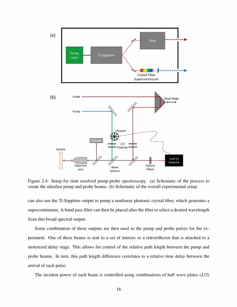
Figure 2.4: Setup for time resolved pump-probe spectroscopy. (a) Schematic of the process tocreate the ultrafast pump and probe beams. (b) Schematic of the overall experimental setup.
can also use the Ti:Sapphire output to pump a nonlinear photonic crystal fiber, which generates a
supercontinuum. A band pass filter can then be placed after the fiber to select a desired wavelength
from this broad spectral output.
Some combination of these outputs are then used as the pump and probe pulses for the ex-
periment. One of these beams is sent to a set of mirrors or a retroreflector that is attached to a
motorized delay stage. This allows for control of the relative path length between the pump and
probe beams. In turn, this path length difference correlates to a relative time delay between the
arrival of each pulse.
The incident power of each beam is controlled using combinations of half wave plates (λ /2)
16

and polarizers. An objective lens is used to both focus the beams onto the sample, as well as collect
and collimate the reflections. This reflection is sent through a beam splitter with a small portion of
the beam sent towards a CCD camera in order to track the position of the laser spots on the sample.
The remaining portions of the beams are sent to a photo-detector. Before reaching the detector,
optical filters are used to block the pump beam so only the reflection of the probe is measured. This
is important, as we want to observe how the pump affects the probe reflection. Thus, the pump
is sent through a mechanical chopper before reaching the sample. The chopper is connected to a
lock-in amplifier which filters out contributions without the chopped frequency. This allows us to
directly measure the portion of the probe reflection that is influenced by the pump.
We then track this differential reflection signal as function of delay stage position. This can be
translated into a delay time by simply using the speed of light and the relative path length change.
As explained earlier, over time, excitons excited by the pump will recombine, opening up more
available states for probe photons to be absorbed, subsequently reducing the reflection. This results
in a measured signal that decays with increasing delay time as a result of exciton recombination.
We can, thus, measure the recombination mechanisms and how the carrier distribution evolves over
time.
For heterostructure samples, we can choose appropriate pump and probe wavelengths to ob-
serve dynamics specific to the different materials. As will be discussed in later chapters, this can
provide insights into both the charge and energy transfer across material boundaries.
2.3 Spatiotemporally Resolved Pump-Probe Spectroscopy
In addition to temporally resolving the differential reflection of the probe, it can also be measured
as a function of pump position to spatially resolve the carrier dynamics. Here, the probe spot is
left stationary to keep the reflection, R0, constant. The pump spot is then moved across sample by
rotating the beam splitter that directs the pump beam into the objective lens. This beam splitter
is equipped with pico-motors, allowing for very precise movement of the pump spot. At each
position of the pump, the differential reflection is measure as a function of the delay time. This
17

Figure 2.5: (a) Schematic of the how the carrier distribution is resolved spatially. (b) Sample spatialprofiles of the differential reflection based on this measurement technique. The blue, purple, andred curves represent the expected evolution of these profiles for later delay times (t1 > t2 > t3). Thewidth of the distribution is expected to increase over time as carriers diffuse outward.
general concept is shown in Fig. 2.5. The blue and red circles in (a) represent the focused pump
and probe laser spots, respectively. An depiction of the measured spatial profiles at different time
steps is shown in (b).
Ultimately, the measured spatial profile represents the convolution of the probe spot and the
carrier density distribution. This can be represented by,
S(x, t) =ˆ
P(x)N(x−µ, t)dµ, (2.1)
where P(x) is the spatial shape of the probe (typically Gaussian), N(x, t) is the injected carrier
density as a function of space and time, and µ is the position of the pump relative to the probe.
If both profiles are Gaussian, then the resulting convolution is also Gaussian113 with a convoluted
18

width,
wS =√
wP2 +wN2. (2.2)
This type of experiment can provide insight into a couple different mechanisms related to
the carrier dynamics. In uniform samples, we can observe the diffusion of the injected carrier
distribution and in non-uniform samples, as with lateral heterostructures, this method can be used
to gain insight into the channels of drift transport. Each will be explained in more detail below.
2.3.1 Photocarrier Diffusion
Typically, in isotropic samples without any external fields present, the transport of injected carriers
is dictated strictly by the density gradient. With an initial Gaussian profile, consistent with the
shape of the pump spot, the carrier distribution will spread radially outward from the injection
site114;115. This is a simple diffusion process that follows the diffusion equation,
∂N(r, t)∂ t
= D∂ 2N(r, t)
∂ r2 , (2.3)
where D is the diffusion coefficient, which is assumed to be a constant with dimensions of area
per time. In uniform 2D samples, the injection depth of the laser spot is far greater than the
sample thickness and thus allows us to consider only planar diffusion. If this diffusion is then
also isotropic, we can mathematically treat the injected carrier density in 1D, with a Gaussian
distribution,
N(x, t) =N0
w(t)√
2πe−
12 (
xw(t) )
2, (2.4)
with w(t) representing the time-dependent width of the distribution. It can be shown that the
squared width depends linearly on time as,
19

w2(t) = w20 +2Dt, (2.5)
satisfies the diffusion equation, with w0 being the initial width of the distribution. This can then be
translated to a FWHM by,
FWHM = 2√
2ln(2)w, (2.6)
making the squared width,
w2(t) = w20 +16ln(2)Dt ≈ w2
0 +11.09Dt. (2.7)
We can then track the squared width of the measured spatial profile as a function of the delay
time to find the diffusion coefficient for injected photocarriers in the sample. It is important to note
that this treatment of the diffusion process does not take into account the recombination rate of
the injected carriers. Ultimately, any decay of the signal due to recombination does not affect the
spatial component of the distribution. This leaves the width of the distribution unchanged by the
recombination process.
The extracted diffusion coefficient, D, along with the photocarrier lifetime, τ , can then be used
to infer other material properties. The diffusion length can be found by,
L =√
Dτ. (2.8)
Important to electronic applications is the carrier mobility as it is essentially a measure of how well
carriers move within a material. The diffusion coefficient is related to mobility by the Einstein
relation,
Dµ
=kBT
e, (2.9)
with kB being the Boltzmann constant, T the sample temperature, and e the elementary charge.
20

2.3.2 Photocarrier Drift
In the case of non-uniform samples or when there is an externally applied electric field, many of the
assumptions used in the previous section no longer hold. In many regards, this is because there are
now different mechanisms present. For example, in photodiodes and photovoltaic (PV) devices,
there is an applied voltage across the material that leads to charge separation of injected electron-
hole pairs. These separated charge carriers then travel in opposite directions to their respective
terminals. This type of transport is dictated by the electric field as compared to the density gradient,
and is called drift transport. The drift velocity can be found by,
vd = µE (2.10)
where µ is the carrier mobility, and E is the electric field strength.
Another type of drift transport can occur with Dexter energy transport processes, where both
types of charge carriers move in the same direction across a junction. Here, it becomes exciton
drift as a result of the built-in potentials within the structure. Both of these drift mechanisms
can be observed by spatiotemporally resolved pump probe experiments as outlined in Fig. 2.6.
The experimental setup, in this case, is exactly the same as in the previous subsection. The only
difference is that now the carrier distribution undergoes a drift process that causes it to move over
time. Fig. 2.6(a) shows how the distribution would be expected to change if there is roughly
uniform charge separation. Here, the different peaks would actually represent the movement of
electrons and holes separately. Fig. 2.6(b) depicts the case of exciton transport, where the bound
electron-hole pairs move in a singular direction.
In both cases, the distribution still undergoes a diffusion process and thus can be described by
the Fokker-Planck equation, which is often used to describe systems that undergo a combination
of drift and diffusion processes. In 1D, this equation is given by,
∂
∂ t[N(x, t)] =− ∂
∂x[ρ(x, t)N(x, t)]+
∂ 2
∂x2 [D(x, t)N(x, t)] (2.11)
21

Figure 2.6: Expected spatial profiles for a carrier distribution undergoing different drift transportprocesses. (a) An applied electric field causes charge separation. The distribution will then splitwith two peaks representing their respective carriers. (b) Exciton drift causes the whole distributionto move in one direction.
where ρ(x, t) describes the drift process and D(x, t) the diffusion process.
22

Chapter 3
Vertical Heterostructures Formed by Monolayer TMDs
As discussed in Chapter 1, the most prevalent and widely studied type of heterostructure in flat land
is the layered, vdWs heterostructure. In these structures, different materials can be stacked on top
of one another, adhering only by the relatively weak vdWs force. One of the main advantages of
these heterostructures is the lack of chemical bonding at the interface, which allows for different
layered materials to be combined without much concern for lattice matching. This chapter will
look at studies involving 3 different TMD-TMD vertical heterostructures. The first explores trion
formation in a structure formed by stacking MLs of MoSe2 and WS2. Here, common to most
TMD-TMD heterostructures, type-II band alignment facilitates charge separation leading to trion
formation in WS2. Then, carrier dynamics are examined in two heterostructures that contain less
common TMD MLs. These two heterostructures, WSe2-MoTe2 and MoS2-ReS2, are predicted and
found to exhibit type-I band alignment facilitating exciton transfer across their respective junctions.
3.1 Trion Formation in Type-II MoSe2-WS2 vdWs Heterostructure
One of the prominent features of TMD MLs is strong electron and hole interactions as a result of
reduced dielectric screening from the low dimensionality. This leads to strongly bound excitons
with large binding energies on the order of hundreds of meV27;28. Such strong Coulomb interac-
tions in these materials can also lead to charged exciton formation, known as trions. These trions
have been observed mostly at cryogenic temperatures, but can also be induced by gate-doping29,
photoionization of impurities116, different substrates117, or functionalization layers118. This sec-
tion looks at the formation of trions at room temperature in a vertical heterostructure formed by
23

MLs of MoSe2 and WS2. The type-II band alignment between these layers facilitates charge sepa-
ration, resulting in excess electrons in WS2. The excited excitons and transferred electrons interact
forming these trions. This is observed by an addition peak in the PL spectra of the heterostructure,
not seen in isolated WS2. We also deduce a zero-density trion binding energy of 62 meV. This
study was published in the journal, ACS Nano119.
3.1.1 Sample Fabrication and Characterization
For the samples fabricated in this experiment, monolayers of both MoSe2 and WS2 were exfoli-
ated onto flexible, transparent polydimethylsiloxane (PDMS) substrates. Monolayers were found
using an optical microscope and initially identified by optical contrast. Then, using a specialized
microscope equipped with long working distance objective lenses and micro-manipulators, the
monolayers are transferred to a Si/SiO2 substrate, one on top of the other. After stacking these
monolayers, as shown in Fig. 3.1, the sample is annealed at 200◦C for 2hrs in an Ar/H2 (100sc-
cm/5sccm) environment with a base pressure of 3 torr. The annealing process helps to clear the
heterostructure of trapped contaminants, providing better coupling between the two layers. The
fabrication process is highlighted in more detail in A.1.
Using the sample described above, PL spectra were taken for both individual monolayers and
the overlapping heterostructure region. The sample was excited using a continuous-wave (CW),
405 nm laser and the resulting luminescence was collected by a Horiba iHR550 imaging spec-
trometer. Figure 3.2 shows the PL spectra of the aforementioned regions, WS2 (blue), MoSe2
(red), and the heterostructure (black). The individual monolayers are found to have peaks at 1.58
eV (MoSe2) and 2.01 eV (WS2), and both have widths of about 50 meV. This is consistent with
previously reported values120–125, and also confirms the ML thickness.
3.1.2 Results and Discussion
There are a few clear differences between the individual monolayer spectra and the heterostructure
spectrum. First, there is a huge quenching (factor of 23) of the WS2 monolayer peak in the het-
24

Figure 3.1: Optical images of the MoSe2-WS2 heterostructure sample at different steps of fabrica-tion. (a,b) Images of the MoSe2 and WS2 monolayer samples on the PDMS substrates. (c) Imageof the MoS2 sample after being transferred to a Si/SiO2 substrate. (d) Image of the heterostructureafter the transfer of the WS2 sample. The scale bars are 20 µm. Reproduced with permission fromACS Nano 2015 9 (6), 6459-6464. Copyright 2015 American Chemical Society.
25

Figure 3.2: Photoluminescnece spectra measured from WS2 (blue), MoSe2 (red), and the het-erostructure (black). Reproduced with permission from ACS Nano 2015 9 (6), 6459-6464. Copy-right 2015 American Chemical Society.
erostructure, which is largely believed to be the result of efficient interlayer charge transfer across
the junction. There is also the peak of the indirect exciton, from the recombination of electrons in
the WS2 layer and holes in the MoSe2 layer. A slight broadening of this peak is from the quenched
MoSe2 peak. Lastly, the additional bump next to the WS2 peak is believed to be due to the forma-
tion of trions, and is the primary focus fo this study. As shown in Fig. 3.3, trion formation, often
referred to as charged excitons, are formed in the WS2 layer as electrons are transferred from the
MoSe2 layer.
The type-II band alignment stimulates charge separation in the heterostructure leading to an
excess of electrons in the WS2 layer and an excess of holes in the MoSe2 layer. The PL peak repre-
senting these trions is shifted from the WS2 peak as a result of the extra binding energy associated
with the excess electron. To extract this binding energy and learn more about the suspected trion
peak, we excite the heterostructure with different pump powers, as shown in Fig. 3.4. Here, each
dataset is fit with a two Gaussian functions. The red and blue curves in each are the individual
Gaussian fits to the exciton and trion peaks, respectively, with the orange curve representing the
26

Figure 3.3: Expected band alignment of the MoSe2-WS2 heterostructure. Electrons in MoSe2transfer to WS2 creating bound trions. The resulting recombination of these particle clusters resultsin a shifted peak in the PL. Reproduced with permission from ACS Nano 2015 9 (6), 6459-6464.Copyright 2015 American Chemical Society.
cumulative fit.
From these fits we can reliably separate the trion peak from the exciton peak. The peak energy
as a function of the excitation power for the exciton and trion are shown in Figs. 3.5(a,b). Here, we
find with increasing the the excitation level that energies of both peaks decrease. The change in the
trion peak energy (ET ) is noticeably larger than that of the exciton peak (EX ). Taking the difference
of the two, EX −ET , we find that the separation increases linearly with excitation level, shown in
Fig. 3.5(c). This energy difference is known as the trion binding energy, and is the required energy
to separate the trion into an exciton and free electron or hole. The binding energy increases with
the excitation level, because the free charge needs to be released above the Fermi surface where
there are unoccupied states. Increasing the excitation level increases the Fermi surface, and thus
the binding energy as well.
From the linear extrapolation, we find a trion binding energy of 62 ± 2 meV at zero excitation
power. This is slightly larger than previous reports on trions in WS2121;122. It is interesting to note
27

Figure 3.4: Photoluminescence spectra measured from the heterostructure for different pump exci-tation powers. The red and blue curves are Gaussian fits to the exciton and trion peaks respectively.The orange curve is the cumulative fit from the two Gaussian functions. Reproduced with permis-sion from ACS Nano 2015 9 (6), 6459-6464. Copyright 2015 American Chemical Society.
28

Figure 3.5: Power dependent trends from 3.4 (a,b) The peak energy measured from the exciton andtrion peaks as a function of the excitation power. (c) The difference between (a) and (b). (d,e) Theheight of the exciton and trion peaks as a function of excitation power. (f) The ratio of the peakheights found in (d) and (e). Reproduced with permission from ACS Nano 2015 9 (6), 6459-6464.Copyright 2015 American Chemical Society.
that this binding energy is consistent with the conduction band offset (60 meV) in the heterostruc-
ture126.
We also look at how the heights of each peak, HX and HT , change with excitation power. The
results are summarized in Figs. 3.5(d,e). We see that both peaks scale similarly in a super-linear
fashion. The curves shown are fit using a power of about 1.6 in each case. This superlinear depen-
dence is likely the result of defects in the materials which allow for nonradiative recombination
and exciton trapping that can compete with radiative recombination127–129. With higher excitation
powers, a higher portion of injected carriers recombine radiatively as the number of defects is more
or less fixed. In Fig. 3.5(f), we also see that the ratio of the two peak heights is relatively constant
with excitation power.
29

One would also expect to see evidence of trion formation in the MoSe2 layer. The reason we
do not observe this is likely due to a higher density of defect sites in MoSe2 compared to WS2.
Monolayer WS2 is commonly known to have very strong PL yield due to better growth methods
that incur fewer of these defect sites. With fewer defect sites, charge carriers in WS2 can more
easily form both neutral and charged excitons instead of quickly recombining with defects as in
MoSe2.
The results observed in the MoSe2-WS2 heterostructure are a prime example of the charge
transfer phenomena that can be seen in vdWs heterostructures. The type-II band alignment fa-
cilitates one type of electronic control in these atomically thin materials. Next, we will explore
slightly more exotic combinations of TMD MLs layers that exhibit type-I band alignment.
3.2 Exciton Transfer in Type-I vdW Heterostructures
The above study involved one of the more common TMD heterostructures. It exhibited type-II
band alignment, which drives charge separation at the interface. This type of band alignment is
expected from, and has been observed in, all of the heterostructures formed by combinations of the
four common TMD layers, MoS2, MoSe2, WS2, and WSe274;77;79;101;126. However, finding combi-
nations of layered materials that form type-I alignment is essential for many different applications
like ultrathin quantum wells, optical pumping and wavelength conversion devices. Presented here
are two heterostructures formed by combining different TMD MLs that exhibit type-I band align-
ment. We find that the heterostructure with two similar crystal structures facilitates faster transfer
dynamics than the one with dissimilar crystal structures.
3.2.1 2H-2H MoTe2-WSe2
The first type-I heterostructure we look at is formed by vertically stacking monolayers of MoTe2
and WSe2. In this case, each of the materials have a similar 2H crystal lattice.
In our experiments, the WSe2-MoTe2 heterostructure sample was fabricated in a similar fashion
30

Figure 3.6: (a) Optical image of the MoTe2-WSe2 heterostructure sample. (b) Calculated bandalignment between MLs of WSe2 and MoTe2. The orange and gray circles represent excited elec-trons and holes, respectively, which are expected to transfer to the MoTe2 layer.
to the sample in the previous section, by mechanically exfoliating the MLs of WSe2 and MoTe2
onto PDMS substrates and sequentially transferring the layers to a Si/SiO2 (90 nm) substrate. An
optical image of the heterostructure sample is shown in Fig. 3.6(a). Due to the relative instability of
ML MoTe2 in ambient conditions130, this layer was completely covered by the WSe2 ML, in order
to increase the longevity of the heterostructure sample. Isolated ML regions of both materials were
also present on the same substrate in order to conduct a reliable comparison between each ML and
the heterostructure. The sample was also annealed under the same conditions as the sample in the
previous section. The thickness of each ML is determined by optical contrast (outlined in A.2).
A schematic of the calculated band alignment is shown in Figure 3.6(b). With both the CBM
and VBM residing in MoTe2, excitons induced in WSe2 are expected to transfer to MoTe2 where
they recombine, emitting photons (red arrows) with an energy consistent with the optical bandgap
of MoTe2. In the following, we present experimental results on the photocarrier transfer process,
which show unambiguously the type-I nature of the band alignment.
First, PL spectra were taken from the heterostructure, as well as, from both ML regions. As
shown in Fig. 3.7, the spectra of the WSe2 ML (red) and the heterostructure (blue) both show
a peak located around 1.65 eV which is consistent with the A-exciton resonance in WSe234;131.
31

Figure 3.7: Photoluminescence spectroscopy data measured from WSe2 (blue), MoTe2 (red), andthe heterostructure (black).
There is significant quenching of the peak, about 83% measured from the heterostructure region.
This shows a good interface between the two layers, and provides initial evidence that electrons,
holes, or both are likely transferring from WSe2 to MoTe2.
To observe the photocarrier dynamics in the heterostructure, we employed transient absorption
microscopy experiments setup in reflection geometry. In these measurements, a tightly focused
pump pulse of about 100 fs duration was used to excite certain regions of the sample. Then, a
probe pulse, which arrives at the sample after the pump and overlaps in space with the pump
spot, is used to monitor the dynamics of the photocarriers. The differential reflection of the probe,
∆R/R0=(R-R0)/R0, is measured as a function of the relative time delay between the two pulses.
Here, R and R0 represent the reflection of the probe pulse with and without the presence of the
pump, respectively. By choosing the pump and probe photon energies, we can preferentially inject
and detect photocarriers in different layers of the heterostructure sample.
We first study the photocarrier dynamics in ML MoTe2. A 1.65 eV pump pulse with a peak
injected fluence of 8.44 µJ cm−2 was used to excite the MoTe2 ML. Based on the absorption
32

coefficient of bulk MoTe22 for this photon energy, 2.5×10⁷ m−1, the pump fluence corresponds
to an injected photocarrier density of about 4.4×1011 cm−2. The differential reflection of a 1.31
eV probe pulse is then measured for different delay times, and can be seen as the gray squares in
Fig. 3.8. Note that both the pump and the probe photon energies are significantly larger than the
optical bandgap of MoTe2 of about 1.1 eV. The rising of the signal can be modeled by the integral
of a Gaussian function with a FWHM of 0.63 ps, as indicated by the black curve in Figure 3.8.
This rising time is slightly slower than the instrument response time of about 0.4 ps, which can be
attributed to the time it takes for the photocarriers to relax their energy from the injected energy
states to the states coupled to the probe pulse. The decay of the signal after the first 1 ps can be fit
by a bi-exponential function with two time constants of 2.8 and 28 ps, respectively. The short time
constant could be attributed to the energy relaxation of photocarriers from the probed state to the
band edges, while the long time constant gives the photocarrier lifetime.
Using this same procedure, we then measured the differential reflection signal from the het-
erostructure under the same conditions. Since the optical bandgap of ML WSe2 is about 1.65 eV,
the pump is expected to inject photocarriers in both layers, while the 1.3 eV probe should only
sense photocarriers in MoTe2. The result is shown by the blue squares in Fig. 3.8. The magnitude
of the signal is about 7.5 times larger than that of MoTe2, while the temporal shapes of the two are
very similar. The white squares in Fig. 3.8 show the scaled signal from ML MoTe2 (multiplied
by 7.5), which shows that the signal from the heterostructure has a very similar rising time, with
a small lag, and slightly slower initial decay. Furthermore, by bi-exponential fit (purple curve),
the two time constants from the heterostructure measurement are 4.3 and 28 ps, with the long time
constant matching the MoTe2 ML very well.
These features are strong evidence of electron and hole transfer from WSe2 to MoTe2, as a
result of the type-I band alignment shown in Fig. 3.6. First, without carrier transfer, the two
measurements should yield identical results since carriers injected in WSe2 would not be sensed
by the probe. The larger signal observed in the heterostructure sample is induced by photocarriers
transferred from WSe2 to MoTe2. The existence of carrier transfer is also consistent with the PL
33
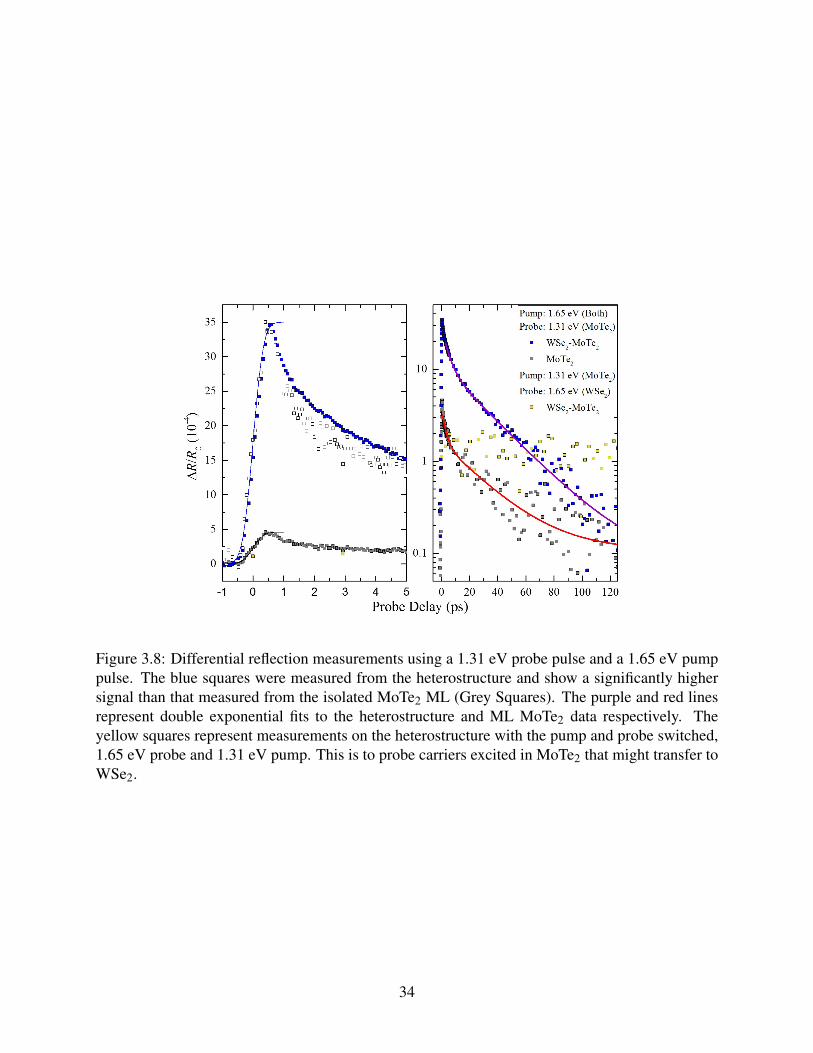
Figure 3.8: Differential reflection measurements using a 1.31 eV probe pulse and a 1.65 eV pumppulse. The blue squares were measured from the heterostructure and show a significantly highersignal than that measured from the isolated MoTe2 ML (Grey Squares). The purple and red linesrepresent double exponential fits to the heterostructure and ML MoTe2 data respectively. Theyellow squares represent measurements on the heterostructure with the pump and probe switched,1.65 eV probe and 1.31 eV pump. This is to probe carriers excited in MoTe2 that might transfer toWSe2.
34

quenching of WSe2, shown in Fig. 3.7. Second, the carrier transfer occurs on a time scale shorter
than the response time of the measurement. If the transfer were a slow process, the signal from the
heterostructure would be expected have a slow rising part as dictated by the transfer rate. Third,
the same decay time observed in the two samples indicates that both electrons and holes excited
in WSe2 transfer to MoTe2, as dictated by the type-I alignment. If the alignment were type-II,
only one type of carrier would transfer. Once the electrons and holes are separated in different
layers, their recombination would be significantly suppressed, resulting in a longer lifetime of
photocarriers in the heterostructure79;132–134.
To ensure that no carriers, neither electrons nor holes, transfer in the opposite direction, i.e.
from MoTe2 to WSe2, we used a 1.31 eV pump and probed at 1.65 eV. In this case, we expect to
inject photocarriers in MoTe2 only. The 1.65 eV probe matches the A-exciton resonance of WSe2
providing the best differential signal from carriers in the WSe2 layer. As shown by the yellow
squares in Fig. 3.8, there is no noticeable signal from the heterostructure observed. It is also
important to note that this signal is from a peak injected fluence of 16.9 µJ cm−2, twice that of the
other 2 curves in Fig. 3.8. With an absorption coefficient of 0.8×10⁷ m−1, this fluence corresponds
to an injected density of 4.5×1011 cm−2. If the band alignment were type-II, there would be charge
separation and we would expect to observe a noticeable differential reflection signal due to either
electrons or holes transferring to WSe2 under these conditions.
To further confirm that the increased signal observed in the heterostructure is from photocarri-
ers injected in WSe2 that subsequently transfer to MoTe2, we studied the dependence on the pump
energy. Using a 1.31 eV probe, we varied the pump energy from 1.65 eV, the A-exciton resonance
of WSe2, to 1.55 eV. Figure 3.9 shows the differential reflection of the heterostructure for the dif-
ferent pump energies. The inset shows the peak signal as a function of the pump energy. It is clear
the signal increases as the pump energy moves towards the exciton resonance of WSe2. This indi-
cates that as more photocarriers are injected in WSe2, subsequently the observed carrier density in
MoTe2 also increases. The trend of this increase is fairly consistent with the energy dependence of
the absorption coefficient in WSe242.
35

Figure 3.9: Pump energy dependence on the differential reflection of 1.31 eV probe measuringthe heterostructure. The inset shows the peak differential reflection signal for the different pumpenergies.
Next, we looked at the carrier dynamics in WSe2. Photocarriers were injected by a 2.1 eV
pump in the WSe2 ML and the heterostructure with a peak fluence of 4.22 µJ cm−2. At this
energy, WSe2 has an absorption coefficient of 1.6×10⁷ m−1, which leads to an injected carrier
density on the order of 1.4×1011 cm−2. From Fig. 3.10, it can be seen that there is an initial fast
decay in the heterostructure that is noticeably faster than the exciton decay in ML WSe2. Fitting
each data set with a bi-exponential function, the initial fast decay is about 0.84 ± 0.3 ps in ML
WSe2 compared to 0.66 ± 0.1 ps in the heterostructure, about a 20 percent decrease. This faster
decay is almost certainly from carriers transferring from WSe2 to MoTe2, another indication of
type-I band alignment. The right panel of Fig. 3.10 shows the dynamics on a longer time scale.
The longer decay times are nearly identical at 33 and 29 ps, respectively. It is also important to
note that the signal from the heterostructure is smaller in magnitude than that of the isolated WSe2
ML. This is evidence that a significant portion of the photocarriers transfer on an ultrafast time
scale, faster than the time resolution of our system of about 300 fs. These transfer dynamics are
consistent with previous reports on TMD heterostructures that point to a coherent transfer process
36

Figure 3.10: Short and long scale differential reflection measurements on WSe2 ML (Blue) andthe heterostructure (Red) using a 1.65 eV probe and 2.1 eV pump.
between layers.
3.2.2 2H-Distorted 1T MoS2-ReS2
The previous section discussed results on a heterostructure comprised of two materials with very
similar lattice constructs, both having hexagonal, 2H, structures. In that heterostructure, as seen in
other 2H-2H vdW heterostructures, we observed ultrafast exciton transfer from one material to the
other. This transport was so fast that it was beyond the response time of our system of about 300 fs.
This section will look at another suspected type-I heterostructure which is formed by combining
two dissimilar crystal structures. In this case, the heterostructure is made from monolayers of
2H-MoS2 and distorted 1T-ReS2. This study was published as the cover article in the journal,
Nanoscale Horizons135.
Similar to the previous structure, the expected band alignment is found from first principle
calculations, which were performed by our collaborators from Dr. Zeng’s group at The University
of Nebraska. In MoS2, the VBM and CBM are found to be -5.91 eV and -4.25 eV, respectively.
37

Figure 3.11: (a) Calculated band alignment of monolayer MoS2 and ReS2. (b) Calculated bandstructure of the MoS2-ReS2 heterosturcture. The red and green symbols represent contributionfrom MoS2 and ReS2, respectively. Reproduced from Ref. 135 with permission from The RoyalChemical Society.
In ReS2, they are -5.78 eV -4.46 eV, respectively, resulting in type-I band alignment between the
layers. Fig. 3.11(a) shows this band alignment. Fig. 3.11(b) shows the calculated band structure
for the heterostructure. Here, the red symbols represent contributions from MoS2, where as the
green is contributions from ReS2. The calculations shows that both the CBM and VBM in the
heterostructure are contributed from ReS2, predicting the type-I alignment at the junction.
Fabricating this heterostructure followed the same procedure used in the previous section, with
both materials being mechanically exfoliated and transferred onto a 90 nm SiO2/Si substrate. The
sample was then annealed under the same conditions previously mentioned. An optical microscope
image of the final sample is shown in Fig. 3.12(a).
To confirm the ML thickness of the materials, we utilized optical contrast and Raman spec-
troscopy. Figure 3.12(b) shows the green channel contrast measured along the yellow line in (a).
The green channel is used as it provides a good standard for the contrast of various monolayers of
about 12-13%, as shown in previous reports136–138. Our measurements are in agreement with the
expected contrast of ML samples (see A.2).
The Raman spectroscopy results are shown in Fig. 3.12(c) for both MoS2 (red) and ReS2
38

Figure 3.12: (a) Optical image of the MoS2-ReS2 sample. (b) Contrast measured from the greencolor channel along the yellow line in (a). (c) Raman spectra measured from MoS2 (red) andReS2 (green) The large peak at a Raman shift of around 520 cm−1 is from the silicon substrate.Reproduced from Ref. 135 with permission from The Royal Chemical Society.
39

(green). Raman measurements were also used to further confirm monolayer thickness of both
layers. In MoS2 the separation between the E12g and A1g peaks is used to confirm the ML thick-
ness139. For ReS2, the separation between the peak labeled I and III in Fig. 3.12(c), also point to
ML thickness (see A.3 for a more in-depth look at the Raman modes in both layers).
Now that we have established both layers to be monolayer,as expected, we again look at the
injected carrier dynamics using transient absorption microscopy to measure the time dependent
differential reflection. First, using a pump pulse with an energy of 1.67 eV and 300 fs duration, we
inject carriers in a portion of the ReS2 monolayer. Because the optical band gap of Re2 is about
1.52 eV, these carriers are injected by inter-band absorption. We focus the laser spot through a 20×
objective lens to a spot size of 2.2 µm, injecting carriers with a fluence of 7 µJ cm−2. With an
absorption coefficient of 8 × 10⁶ m−1 (bulk value), we obtain a peak injected density of about 1.4
× 1011 cm−2. We monitor the dynamics of these carriers by measuring the differential reflection
of a 1.53 eV probe pulse. This is tuned slightly above the bandgap of ReS2. The open red squares
in Fig. 3.13, show the results of this experiment. We fit the decay of the signal using a single-
exponential with a background. From this, we find a decay constant of 65±5 ps which is attributed
to the recombination lifetime of the photocarriers. Similar results were observed when measuring
the heterostructure region of the sample shown by the solid red squares in Fig. 3.13.
In this experiment on the heterostructure, the MoS2 was neither pumped nor probed, as the
lowest excitonic state in MoS2 is at 1.85 eV. If the band alignment were type-II, however, we would
expect to see a change to the measured dynamics as the MoS2 layer would serve as a channel for
charge transfer. Specifically, if the CBM (VBM) were lower (higher) in MoS2 compared to ReS2,
electrons (holes) would be expected to transfer to MoS2. This would results in a smaller magnitude
of the signal (by about a factor of 2) due to the loss of one carrier type in ReS2. We would
also expect to see a longer carrier lifetime from indirect exciton formation across the junction as
observed from other type-II heterostructures79;101;132.
However, the lack of charge transfer is not itself proof of type-I band alignment, as poor inter-
face quality could be a factor. TO rule this out, we next inject carriers in both ReS2 and MoS2 using
40

a 1.85 eV pump. This is tuned to the A-exciton resonance of MoS2. We again inject carriers with
a peak fluence of 7 µJ cm−2, resulting in peak density of 4.8 × 1011 cm−2. This is according to an
absorption coefficient of 3 × 10⁷ m−1 for MoS2. Measuring the differential reflection of the same
1.53 eV probe, we would expect to see an increase in the signal measured from the heterostructure
if there is type-I band alignment. The results are shown by the solid green squares in Fig. 3.13.
We indeed see an increase of the signal, by a factor of 3, and the decay is also very similar to that
of the ReS2 monolayer, with a time constant of 62 ps (blue curve).
Using this more energetic pump, we also again measure the isolated ReS2 monolayer, as shown
by the open green squares in Fig. 3.13. Here, we do not see an increase in the signal magnitude
which confirms that the increased signal from the heterostructure is not from addition carriers
injected in ReS2 due the increased pump energy. This signal is very similar to that measured
with the 1.67 eV pump confirming that the signal from ReS2 is rather insensitive to the the pump
photon energy in this range. This is consistent with other observation that the absorption coefficient
in ReS2 does not change significantly in this range as well.
To provide further evidence of the type-I band alignment between these two layers, we also
probe the MoS2 layer. Here, we measure the differential reflection of a 1.85 eV probe, matching
the A-exciton of monolayer MoS2. The results are summarized in Fig. 3.14. First, using a 3.06 eV
pump, we inject carriers in MoS2 with fluence of 12 µJ cm−2. With an absorption coefficient of
1.5 × 10⁸ m−1, this corresponds to an estimated injected density of 3.4 × 1012 cm−2. The results
are shown as the solid black squares in Fig. 3.14. We observe a differential reflection signal on the
order of 10−3.
Next, using a 1.53 eV pump, we inject carriers in the ReS2 layer of the heterostructure, with
a fluence of 33 µJ cm−2. This corresponds to a peak injected density in ReS2 of 7.6 × 10¹¹.
If the band alignment were type-II, electrons or holes would transfer to MoS2. Given the fairly
high injected carrier density, these transferred carriers would be expected to result in a differential
reflection signal on the order 10−4, using a 1.85 eV probe. However, as shown by the open squares
in Fig. 3.14, no such signal is observed. This further confirms a lack of charge transfer from ReS2
41

Figure 3.13: Differential reflection of a 1.53 eV probe measured from ML ReS2 (open symbols)and the MoS2-Res2 heterostructure (closed symbols) for different pump energies, 1.57 eV (redsymbols) and 1.85 eV (green symbols). Reproduced from Ref. 135 with permission from TheRoyal Chemical Society.
42

Figure 3.14: Differential reflection of a 1.85 eV probe as a function of probe delay. The blacksquares represent the measurements from ML MoS2 using a 3.06 eV pump. The white squaresrepresent the measurements from the heterostructure using a 1.53 eV pump to excite carriers onlyin the ReS2 layer. Reproduced from Ref. 135 with permission from The Royal Chemical Society.
to MoS2.
Finally, with the confirmed observation of type-I band alignment exhibited by this heterostruc-
ture, we can study the interlayer transfer process of photocarriers in this configuration. These
results are outlined in Fig. 3.15. In this figure, all the differential reflection signals are normal-
ized in order to facilitate a visual comparison. First, a 1.85 eV pulse with a peak fluence of 7 µJ
cm−2 was used ot pump the heterostructure. Based on the absorption coefficients of each of the
monolayers, the peak density of injected photocarriers in MoS2 and ReS2 are 4.8× 1011 cm−2 and
1.3 × 1011 cm−2, respectively. Probing the ReS2 layer with a 1.53 eV pulse, we monitored the
evolution of the photocarrier population in that layer and hence time resolved the transfer process.
In Fig. 3.14, the solid and open green squares represent the measurements from this configuration
as observed from the heterostructure and monolayer ReS2, respectively. We found a rather slow
rise of the signal observed from the heterostructure. The contribution of photocarriers directly
injected in ReS2 can be isolated by the control experiment on monolayer ReS2 under the same
43

experimental conditions. The actual magnitude of the signal measured in ReS2 is about one third
that from the heterostructure, which is consistent with the ratio of the carriers injected in the two
layers. Clearly, the rising of the signal is much faster in ReS2, confirming that the slower rise time
observe from the heterostructure originates from the transfer of photocarriers across the interface.
We fit the rising part of the signal using,
N1[1− exp(−t/τT )]+N2, (3.1)
where N1 and N2 represent the initial photocarrier densities in the MoS2 and ReS2 layers, respec-
tively, and, τT represents the transfer time. As shown by the green line in Fig. 3.15, this expression
can satisfactorily describe the data with a transfer time of 1.3 ± 0.1 ps.
Alternative to observing the photocarrier build up in ReS2, we also monitor the photocarrier
population leaving the MoS2 layer of the heterostructure. Using a 3.06 eV pump pulse, we inject
photocarriers in the heterostructure and probe the MoS2 layer with a 1.85 eV probe. Carriers in
ReS2 are not sensed by this probe. The results are shown as the blue squares in Fig. 3.15. The
signal decays single-exponentially with a decay constant of 1.1 ± 0.2 ps, as indicated by the blue
curve. The decay is significantly faster than that observed from monolayer MoS2 under the same
conditions (black squares in Fig. 3.14), which represents the exciton recombination time. This fast
decay is due to the transfer of photocarriers to the ReS2 layer, and the time constant very closely
matches the transfer time, τT , observed in the build up of photocarriers in ReS2.
Several studies on other TMD heterostructures, including the results in the previous subsection,
have shown that transfer processes in these ultrathin structures occurs on a time scale shorter than
100 fs78;79;101. This ultrafast process is thought to be facilitated by quantum coherence. The
transfer process in this heterostructure, however, is noticeably slower, occurring on a ps time scale.
The most notable difference between this heterostructure and the others is the difference in crystal
structures. In each of the previous studies, the two layer each have the same 2H crystal structure.
Here, the heterostructure is formed by MoS2 with a 2H structure and ReS2, which has a distorted
1T structure. It is possible that difference in lattice structures suppresses the coherent transfer
44
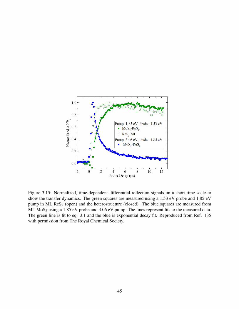
Figure 3.15: Normalized, time-dependent differential reflection signals on a short time scale toshow the transfer dynamics. The green squares are measured using a 1.53 eV probe and 1.85 eVpump in ML ReS2 (open) and the heterostructure (closed). The blue squares are measured fromML MoS2 using a 1.85 eV probe and 3.06 eV pump. The lines represent fits to the measured data.The green line is fit to eq. 3.1 and the blue is exponential decay fit. Reproduced from Ref. 135with permission from The Royal Chemical Society.
45

process, resulting in a slower incoherent transfer process.
3.3 Summary
The experimental observation of Type-I aligned heterostructures in the landscape of vdWs het-
erostructures is of critical importance for the broader applications of 2D materials. These studies
help to introduce the possibility for quantum well applications at the atomic limit which could
prove pivotal for future developments in laser technologies, wavelength manipulation and more.
Most notably, ultrathin semiconducting structures that can combine different types of band align-
ment, will provide unprecedented opportunities to control charge transport on an atomic scale.
The above studies help to initiate a thorough platform for the development of band engineering
at an atomic level, highlighting different types of band alignment, as well as possible effects due
to differences in crystal structures. We found that the charge separation found in the combination
of MoSe2 and WS2, can lead to exotic excitonic behavior with the formation of charged excitons
called trions. We also observed the photocarrier dynamics in two heterostructures, WSe2-MoTe2
and MoS2-ReS2, which both exhibited properties consistent with type-I band alignment, facilitat-
ing exciton transfer across the junction.
We also observed a noticeable difference in the transfer time seen from the two type-I struc-
tures. We believe this to be the results of different crystal structures. The WSe2-MoTe2 het-
erostructure is formed by two layers with similar 2H crystal structures. As seen in other similar
2H-2H heterostructures, this results in a transfer process shorter than 100 fs, facilitated by quantum
coherence. The MoS2-ReS2 heterostructure has a 2H-Dist. 1T combination that results in a much
slower transfer process, on the order of 1 ps. This difference in crystal structure likely breaks the
coherence, resulting in slower photocarrier transfer.
46
Chapter 4
2D Amorphous-Crystalline Semiconducting Heterostructures
After exploring various TMD-TMD vertical heterostructures, we now shift the focus to another
type of vertical heterostructure, between a TMD monolayer and an ultrathin amorphous semicon-
ductor layer. It is important to look at unique heterostructures formed between different lattice
structures to learn more about the mechanisms that facilitate charge and energy transfer in these
low dimensional systems. In the previous chapter, for instance, it was shown that a heterostructure
with similar lattice structures showed faster energy transfer than one with dissimilar lattice struc-
tures. Studies have shown that charge transfer mechanisms in various TMD-TMD heterostructures
are likely dictated by quantum coherence and effective coupling between donor and accepter states
which reside in opposite layers79;107. Previously, it was assumed that these vdWs structures would
exhibit incoherent transfer due to suspected weak interlayer coupling and relatively large interfacial
spacing compared to chemically bound structures.
Recently, the effect of layer-coupled states has been explored in TMD homobilayers109;140. In
these the structures, the individual layers constitute a perfect lattice match. The results suggest
that it is likely states in the Q or Γ valleys are coupled between layers and could be a dominant
mechanism for ultrafast transfer processes. If these layer-coupled states are responsible for ultrafast
transfer, it would imply that similar efficient transfer would not occur in layered combinations with
significantly different lattice structures. It is thus interesting to study the heterostructure between
2D crystalline and amorphous layers, as it presents an extreme case for exploring this hypothesis.
However, due to the lack of studies on amorphous materials in the 2D realm and specifically
amorphous black phosphorus (aBP), the material used in our study, we will begin by examining
properties of aBP thin films. This will include samples of different thicknesses of 2, 5, and 10
47

Figure 4.1: Top and side view of the lattice structure of (a) crystalline and (b) amorphous blackphosphorus.
nm. Once we establish an understanding for the aBP films, we will look at the interaction of
photocarriers between a TMD ML and the thinnest of these amorphous sheets. The resulting
charge transfer phenomena will be explored in detail.
4.1 Introduction to Amorphous Semiconductors
Amorphous semiconductors are of great importance in the electronics industry. They are an inter-
esting class of materials, as their amorphous structure omits one of the most fundamental charac-
teristics utilized in solid state physics, crystallinity. The difference in structure is highlighted in
Fig. 4.1. This shows the lattice structure of crystalline (a) and amorphous (b) black phosphorus,
the material studied in this chapter. Here, in a stable crystalline form, BP exhibits a puckered
hexagonal structure14, where as the amorphous form, by nature, is much more randomized.
In amorphous solids, this lack of long-range periodicity often leads to very fuzzy electronic
states and poor electronic performance compared to their crystalline counterparts. However, low
fabrication costs makes these types of materials highly desirable for applications that do not re-
quire superior performance. Most notably, amorphous silicon has been widely used for common
48

photovoltaic devices141 and thin-film transistors142. Amorphous In-Ga-Zn-O has shown promise
for transparent thin-film transistors with reported mobilities exceeding 10 cm2 V−1 s−1 143. Addi-
tionally, amorphous SiO2 is widely used as a gate dielectric in the electronics industry. Tin-based
oxides have been used in lithium-ion storage applications144. Amorphous materials have also been
used as reaction catalysts, with amorphous iron being used to aid in the hydrogenation of carbon
monoxide145, and amorphous metal-oxides as an oxygen evolution reaction catalyst146.
The majority of applications utilizing amorphous solids to date have focused on bulk mate-
rials. Knowing that ultrathin, 2D materials can exhibit varying properties from their bulk, 3D
counterparts, it is important to investigate 2D amorphous materials. It would be expected that
the electronic properties in dramatically thinned down amorphous semiconductors should follow
similar trends to crystalline 2D materials as many of the differences from bulk to ML spawn from
dielectric screening and confinement effects. These types of effects are not unique to crystalline
materials.
The following sections will focus on studies involving amorphous black phosphorus. The
motivation behind studying ultrathin films of aBP spurs from the promising attributes of crystalline
black phosphorus. Layered black phosphorus (BP) has received an increasing amount of interest
as a 2D semiconductor in recent years, especially with the ability to isolate layers down to ML147.
Ultrathin BP films have exhibited very promising charge transport properties147;148;148–156. Along
with novel quantum confinement effects157;158, crystalline BP has shown a variable band gap that
changes with thickness. This gap has been shown to dramatically increase from 0.35 eV in bulk
to the near IR and even optical range in ML147;159–162. We will look at 3 different thicknesses
of aBP films, 2, 5, and 10 nm. A previous study163 performed by our collaborators, has looked
at various properties of these thin films and found field effect mobilities of 14 cm2 V−1 s−1 and
current On/Off ratios of about 100. This gives some promise or potential applications as thin film
transistors. The following will focus on the photocarrier dynamics in these materials as studied by
ultrafast pump-probe experiments. This study is published in the journal, 2D Materials164.
49

4.2 Carrier Dynamics in Amorphous Black Phosphorus Thin Films
4.2.1 Fabrication and Characterization of aBP thin Films
Amorphous black phosphorus ultrathin films were synthesized on silicon substrates with a 300
nm oxide layer by pulsed laser deposition (PLD). A black phosphorus crystal (Smart-Element)
was used as the target. The growth temperature was set at 150 ◦C and the base pressure of the
chamber was evacuated to around 1.5× 10⁻⁷ Torr. Due to the instability of BP in air, a thin
layer of poly(methyl methacrylate) (PMMA) was applied to protect the a-BP films. These samples
were provided and characterized by Shu Ping Lau and co-workers at The Hong Kong Polytechnic
University.
The structure of the as-grown films was characterized by transmission electron microscopy
(TEM) and X-ray diffraction (XRD). From the energy-dispersive X-ray spectroscopy (EDX) re-
sults shown in Figure 4.2(a), the chemical composition of pure phosphorus (P) was confirmed. The
minor peaks of copper (Cu) are attributed to the TEM grid. The amorphous nature of the samples
was indicated by the high-resolution TEM (HRTEM) and XRD as illustrated in Figure 4.2(b) and
4.2(c) respectively. The films were further characterized by Raman spectroscopy. As shown in
Figure 4.2(d), three BP characteristic peaks were observed in the Raman spectra of the aBP thin
films with thicknesses of 2, 5, and 10 nm. As the thickness decreases, the peaks become broader
and the intensity decreases significantly. For the 2 nm thick sample, the Raman peaks exhibit a
shift of about 5 cm−1 with respect to the thicker films, which is consistent with the previous re-
port163. This can be attributed to the consideration that for ultrathin films, the vibrational modes
are more easily influenced by the highly disordered structure. Finally, the optical properties of the
films were also characterized. The room temperature photoluminescence (PL) spectrum of the 2
nm aBP film is shown in Figure 4.2(e). A 808 nm laser was used as the excitation light source.
The emission peak is located at 0.85 eV, which is attributed to the optical band gap of 2 nm aBP.
No PL was observed from the 5 and 10 nm films, suggesting that their optical band gaps are not in
this spectral range.
50

Figure 4.2: Structural characterization and optical properties of the a-BP thin films. (a) EDXspectrum of the aBP thin films, confirming that pure phosphorus films were obtained. (b) High-resolution TEM image of the 10-nm a-BP film, combining the SAED pattern shown inset, revealingthe highly disordered feature of the obtained films. (c) XRD pattern of the a-BP film grown onSiO2/Si substrate. The only emerged peak is Si (400), further confirming the amorphous nature ofthe BP film. (d) Raman spectra of the aBP thin films with different thicknesses. (e) PL spectrumof the 2 nm aBP film under the excitation of an 808 nm laser. c©IOP Publishing. Reproduced withpermission. All rights reserved.
51

4.2.2 Results and Discussion
Transient reflection measurements were performed to investigate photocarrier dynamics in the
grown aBP samples. We will first focus on the 2 nm film. Figure 4.3(a) illustrates the pump-
probe scheme of the measurement. The sample was excited by a 100 fs pump pulse with a photon
energy of 1.57 eV. The probe pulse with a photon energy of 0.80 eV is tuned to near the optical
band gap of the sample in order to effectively sense the reflectance change of the sample induced
by the pump-injected photocarriers. The differential reflection of the probe was measured as a
function the delay time between the pump and probe pulses. Figures 4.3(b and c) show the ob-
served differential reflection signal, in short and long time ranges, respectively, with various values
of pump fluence. We found that the signals reach their peaks on an ultrafast time scale, and then
decay exponentially.
To understand the observed features, we first establish the relation between the signal and
the photocarrier density. Figure 4.3(d) shows the peak signal as a function of the pump fluence.
With the fluences lower than 100 µJ cm−2, the absorption of the pump can be safely assumed
to be in the linear regime. Hence, the carrier density injected by the pump is proportional to the
pump fluence. That is, the dependence of the signal on the pump fluence reflects its dependence
on the photocarrier density. Figure 4.3(d) shows saturation effect of the differential reflection at
fluences higher than 50 µJ cm−2. The fluence dependence can be fit by a standard saturation
model, ∆R/R0 ∝ F/(F +Fsat), where Fsat = 350 µJ cm−2 is the saturation fluence. Below 50 µJ
cm−2, the differential reflection is approximately proportional to the pump fluence, and hence the
photocarrier density.
With an excess energy of 0.72 eV, the pump pulse injected free electron-hole pairs with high
kinetic energy. As shown in Figure 4.3(b), the signal reaches the peak on an ultrafast time scale,
even though the probe is tuned to near the optical band gap. The rising part of the signal can
be modeled by the integral of a Gaussian function with a full width of 0.45 ps, which is similar
to (or slightly larger than) the cross-correlation width of the pump and probe pulses used. The
initially injected non-equilibrium distributions of the electrons and holes are expected to undergo
52

Figure 4.3: Differential reflection of then 2 nm aBP ultrathin film. (a) Schematics of pump andprobe scheme with respect to the electronic bands of the 2 nm aBP film. (b) Differential reflectionof the 2 nm aBP film for different values of pump fluence. (c) Same as (b), but on a larger timerange and in semi-logarithm scale (d) Peak ∆R/R0 signal as a function of pump fluence. Thesolid line shows a fit to a standard saturation model. (e) The decay times, t1 (black) and t2 (red),obtained from from double exponential fits of the data in (c) as a function of pump fluence. c©IOPPublishing. Reproduced with permission. All rights reserved.
53

a thermalization process first, in which a thermal distribution is established via electron-electron
and hole-hole scattering, followed by an energy relaxation process via carrier-phonon scattering, in
which these hot carriers cool down to the lattice temperature of 300 K. Both processes increase the
population of carriers in the probed states near the band edge, and hence are expected to cause an
increase of the signal. The observed ultrafast rising time suggests that these processes occur on sub-
picosecond time scales in the aBP ultrathin film. Ultrafast thermalization and energy relaxation of
hot carriers have been observed in other 2D materials, such as transition metal dichalcogenides32
and graphene165;166, which can be attributed to the enhanced carrier-carrier and carrier-phonon
interactions due to the reduced dielectric screening effect. Since such enhancement also exists in
ultrathin a-BP, it is reasonable that these processes occur on a similar time scale. On the other
hand, carrier thermalization and relaxation can take several tens of picoseconds in traditional bulk
semiconductors and quantum wells167.
The decay of the signal can be fit by double exponential functions, as shown by the solid
curves in Figure 4.3(b) and 4.3(c). The two constants are plotted as a function of the pump fluence
in Figure 4.3(e). The fast time constant of about 2 ps could be attributed to exciton formation. Due
to the enhanced coulomb interaction between electrons and holes in this 2D system, the exciton
binding energy is expected to be large, and excitons should be stable at room temperature. Ultrafast
exciton formation from nonresonantly excited electron-hole pairs has been observed in monolayer
transition metal dichalcogenides, as a fast decay of the transient reflection signal shorter than 1
ps33;168. After this short transient in the first few picoseconds, the rest of the decay can be described
by a time constant of about 400 ± 20 ps, which is attributed to the exciton lifetime. We note that
the longer time constants at high pump fluences could be attributed to the nonlinear dependence of
the signal on the carrier density, as shown in Figure 4.3(d). In that regime, the time evolution of
the differential reflection signal does not accurately reflect that of the carrier density.
It is interesting to note that even in the saturation regime, there is no sign of exciton-exciton
annihilation. Previous studies have shown that exciton-exciton annihilation dominates dynam-
ics of high density exciton populations in 2D TMDs169–172. In our measurement, the injected
54

exciton density is comparable to the saturation density, as evident by the sub-linear power depen-
dence shown in Figure 4.3(d). In this regime, exciton-exciton scattering is expected to be strong.
Exciton-exciton annihilation caused faster decay of exciton population at higher density, which is
not observed in Figure 4.3(c). The absence of exciton-exciton annihilation suggests that the defect
density of the aBP sample is rather high. This is also consistent with the relatively long exciton
lifetime compared to most 2D TMDs.
To study the transport properties of excitons in aBP, we performed spatially resolved differ-
ential reflection measurements. Using the focused 1.57 eV pump pulse, we inject carriers in the
aBP samples with a Gaussian profile of 2.5 µm full width at half maximum. Due to the induced
density gradient, excitons diffuse two-dimensionally. We do not consider a 3D diffusion as the
samples are thinner than the injection depth of the lasers and thus carriers are injected throughout
the sample thickness and diffuse in a planar direction. We then measured the differential reflection
as a function of both probe position and time delay, relative to the pump.
The result of this spatiotemporal measurement for the 2 nm aBP sample is shown in Figure
4.4(a). Here, the probe position is defined as the distance between the centers of the pump and
probe spots. As the excitons diffuse, the spatial Gaussian profile can be seen to expand, showing a
clear sign of diffusive transport. Figure 4.4(b) shows the Gaussian profiles for several probe delays.
Each profile was fit with a Gaussian function to extract its full width at half maximum. The squared
width, w2, is plotted as a function of the probe delay in Figure 4.4(c). In the diffusion process with
an initial Gaussian density profile, the width of the profile expands as w2 = w20 +11.09Dt, where
w0 is the initial width and D, the diffusion coefficient of the excitons. With a linear fit to the
squared widths in Figure 4.4(c), we find a diffusion coefficient of about 5.3 ± 0.2 cm2 s−1. By
using the exciton lifetime of 400 ps, we obtain a diffusion length of√
Dτ = 460 nm.
The exciton diffusion coefficient obtained is significantly larger than other amorphous semicon-
ductors. For example, in amorphous silicon, the most widely used amorphous semiconductor, the
photocarrier diffusion coefficient is on the order of 0.01 to 0.001 cm2 s−1 173–176. Using Einstein’s
relation, µ/e = D/kBt, where µ , e, and kB are the mobility, the elementary charge, and Boltzmann
55

Figure 4.4: Exciton diffusion in the 2 nm aBP ultrathin film measured by spatially resolved dif-ferential reflection. (a) Spatiotemporal differential reflection signal. (b) Spatial Gaussian profilesfor different delay times. (c) The squared width of the Gaussian profiles as a function of the probedelay. The data is fit with a linear function in order to extract the diffusion coefficient from theslope. c©IOP Publishing. Reproduced with permission. All rights reserved.
56

constant, respectively, we deduce an exciton mobility of 200 ± 10 cm2 V−1 s−1. These superior
photocarrier transport properties make aBP an attractive amorphous materials for optoelectronic
applications.
Similar experiments were performed on both the 5 nm and 10 nm aBP film. Figure 4.5(a)
shows, again, the differential reflection of a 0.80 eV probe pulse for different relative time delays of
the 1.57 eV 100 fs pump pulse as measured for the varying aBP thicknesses, 2 nm (black squares),
5 nm (red squares), 10 nm (blue squares). It can be clearly seen that the longer decay portion of
the signal, which more accurately represents the exciton population in the sample is significantly
larger in the 2 nm sample. This is likely due to the probe energy more closely matching the exciton
resonance for this thickness of aBP. Similar to crystalline BP, we expect the band gap of aBP to
significantly depend on sample thickness, likely decreasing with thickness. It is also not surprising
that we observe a more prominent transient process in the first several ps in the thicker samples, as
the pump energy is higher relative the gap energy.
We also performed spatially and temporally resolved differential reflection measurements on
both the 5 nm and 10 nm aBP samples, in order to measure their respective diffusion coefficients.
These results on the 5 nm and 10 nm samples can be seen in Figures 4.5(b) and 4.5(c), respectively.
The squared FWHM, found by fitting the spatiotemporal data with Gaussian functions for the
different relative delay times between the pump and probe pulses can be seen in Figure 4.5(d).
The results from the 2 nm sample (black squares) is added for comparison. As before, all three
datasets were linearly fit in order to extract the diffusion coefficients from the respective slopes. It
can clearly be seen that the slope decreases with thickness of a-BP. Excitons were found to diffuse
in the 5 nm film with a diffusion coefficient of 3.4 ± 0.4 cm2 s−1. This corresponds to an exciton
mobility of about 130 cm2 V−1 s−1. It is interesting to note that there is no diffusion observed in
the 10 nm thick sample.
In summary, charge carrier dynamics were measured in amorphous black phosphorus. Optical
pump probe experiments were utilized to resolve the differential reflection of an ultrafast probe
pulse in both space and time. We found the exciton lifetime to be as high as 400 ps in 2 nm thick
57

Figure 4.5: Differential reflection and exciton diffusion in the 5 and 10 nm aBP ultrathin films (a)Differential reflection of the 2, 5, and 10 nm aBP thin films plotted on a log scale vs relative probedelay. (b) Spatiotemporal differential reflection signal of the 5 nm aBP film (c) Spatiotemporaldifferential reflection signal of the 10 nm aBP film (d) The squared width of the Gaussian profilesas a function of the probe delay for the 2, 5, and 10 nm aBP films. Each dataset is fit with a linearfunction in order to extract the diffusion coefficient from the slope. c©IOP Publishing. Reproducedwith permission. All rights reserved.
58

aBP samples, decreasing in thicker samples. The diffusion coefficients were also extracted and
found to be in the range of 3-6 cm2 s−1 for 2 nm and 5 nm thick samples. This corresponds to
exciton mobilities on the order of 100-200 cm2 V−1 s−1, which is about 2 orders of magnitude
larger than many amorphous semiconductors currently used in a variety of applications. Amor-
phous black phosphorus could thus have a lot of potential for less expensive, better performing
electronic and optoelectronic devices.
4.3 Carrier Transfer in 2D WS2-aBP Vertical Heterostructure
With the promising characteristics of these amorphous samples, it is important to explore avenues
for possible applications. One such direction is to use them in semiconducting heterostructures.
However, it is typically difficult to find ideal growth conditions to create a quality semiconducting
junction with an amorphous sample. Layered materials provide a unique solution to this problem
since they adhere through vdWs forces as compared to chemical bonds. This allows for the easy
formation of such heterostructures, but little is known as to the extent with which the two will
interact, if at all. The following begins to explore the interaction between ultrathin aBP films with
TMD MLs, specifically WS2.
With the largest band gap of the three aBP samples studied previously, the 2 nm aBP sample
provides the best platform for studying carrier dynamics in these ultrathin amorphous-crystalline
heterostructures. Due to the thinness of this sample, it also fits best into the discussion of 2D
semiconductor junctions.
The heterostructure samples are made by mechanically exfoliating and subsequently transfer-
ring ML flakes of WS2 onto the aBP covered substrate. In order to create reasonable control
conditions, we first transferred flakes of hBN with varying thicknesses onto regions of the aBP
substrates. This is done by mechanically exfoliating flakes of hBN from bulk crystals onto PDMS
substrates. The hBN flakes are then transferred onto the aBP covered substrate. Next, monolayer
WS2 samples are similarly exfoliated onto PDMS substrates and identified by optical contrast. Us-
ing the same method as with hBN, they are transferred to the aBP sample, with different regions
59

of the same WS2 flake overlapping both the hBN samples and the aBP substrate. After the WS2 is
transferred, the samples are annealed for 2 hrs at 75◦C in an Ar environment held at a base pressure
of 3 torr. This is to help the van der Waals materials adhere better to the aBP. Next, to help preserve
the aBP surface from degrading in the ambient conditions of our measurements, the samples are
coating in a thin layer of PMMA.
The samples used in this study are shown in Fig. 4.6(a,b). In each, the blue outline is the
ML region of the WS2 sample, and the white outline is the hBN sample. The substrate, which is
shown here as the pinkish colored background, is the aBP covered substrate. Figure 4.6(a) shows
a sample using a relatively thick (>15 layers) hBN flake between WS2 and aBP. This should create
a sufficiently thick insulating barrier allowing us to study the properties of ML WS2. The sample
in Fig. 4.6(b) uses a much thinner barrier, using a few layer (<5 layers) hBN flake. Thicknesses of
the hBN layers are estimated by optical contrast on PDMS.
With so little known about the electronic structure of the aBP samples, such as its work func-
tion, it is difficult to know how carriers will behave in the heterostructure. However, we attempt
to estimate the expected alignment using previously calculated values for the CBM and VBM of
appropriately thick crystalline black phosphorus (BP). Figure 4.7 shows the estimated band align-
ment and the resulting charge transfer.
With both the work function and band gap of BP being highly sensitive to thickness, we use the
values from literature that best represent our 2 nm thick aBP, which correlates to about 3 layers.
Relative to a 0 eV vacuum level, the calculated CBM and VBM for 3 layer BP is found to be about
-4.09 eV and -4.85 eV, respectively177. From reports on the band alignment of various TMD MLs,
the CBM and VBM of WS2 are -3.96 eV and -5.50 eV, respectively126. As shown in Fig. 4.7
this results in type-I band alignment. However, with such a small conduction band offset between
the materials and the ambiguity of aBP’s alignment, we speculate the band alignment could be
either type-I or type-II. With a large valence band offset, holes are expected to transfer from WS2
to aBP, but the uncertainty in CBM alignment leaves us less certain of the transfer of electrons.
It is important to reiterate, however, that much of this is speculation as no studies have yet to be
60

Figure 4.6: (a,b) Optical images of the samples used in this study. ML WS2 is outlined by blue andhBN by white. (a) Optical image of the sample with bulk hBN. (b) Optical image of the sampleusing few layer hBN. (c) Photoluminescence spectroscopy results of ML WS2 on bulk hBN (red),few layer hBN (blue), and directly on aBP (black). The inset shows the normalized PL.
61

Figure 4.7: Estimated band alignment and expected charge transfer of the WS2 and aBP het-erostructure based on the calculated CBM and VBM values from literature. The fairly large va-lence band offset results in hole transfer from WS2 to aBP, whereas with a small conduction bandoffset and relative uncertainty of the true alignment of aBP, the direction of electron transfer is lesscertain. From this, we would expect the band alignment to be either type-I or type-II.
performed on aBP to determine its work function or band alignment.
The WS2 is characterized using photoluminescence spectroscopy. A continuous wave, 405 nm
laser, is focused through a 100× objective lens on to the WS2 sample. As seen in Fig. 4.6(c), the
WS2 placed on thick hBN exhibits a strong luminescent peak at 2.02 eV (red), which is consistent
with previous reports and confirms the ML thickness of the WS2121;122;124;125. There is significant
quenching of this peak, about 95 percent, for the portion of the WS2 placed directly on aBP (black).
This quenching is a likely indication of some sort of charge or energy transfer mechanism from
WS2 to aBP. Without the transfer of carriers, excitons would be expected to stay in WS2 and
recombine, contributing to the PL signal. It is well known that hBN serves as a near ideal substrate
for many 2D materials. It is then possible that some quenching could arise as a result of simply
being placed on a less ideal surface, however, it is hard to justify such a large effect on this basis
alone.
Looking at the sample on thinner hBN (blue), some interesting results arise. First, despite the
62

thin insulating layer, there is still noticeable quenching compared to the sample on thick hBN.
There is also a secondary peak present at 1.97 eV. The emission energy of this peak is consis-
tent with that of charged excitons or trion formation, which has been previously observed in ML
WS2119;178. The presence of trions would suggest that there are either excess electrons or holes
in WS2, pointing towards a charge transfer process. It is interesting to note that this only occurs
in the heterostructure with a thin hBN barrier and not the direct junction, which may indicate a
discernible difference in the transfer mechanisms in the two cases. As briefly discussed in the pre-
vious section, the aBP films are thought to have a fairly high density of defect states, due at least in
part to the amorphous structure. Suppression of radiative recombination due to these defects could
play a role in this difference.
Looking into this further, we examine the emission spectrum for different excitation powers
in the sample on few layer hBN. The different spectra can be seen in Fig. 4.8. In most of these
measurements there are actually 3 discernible peaks. This third peak could be attributed to bi-
exciton formation, where two excitons are bound together. Each spectra is fit for 3 Lorentzian
peaks, except in the 1 µW case, as no third peak was found for unknown reasons. In this case,
the data was fit with a bi-Lorentzian function. The neutral, A-exciton peak of WS2 is the blue
fitted curve, with the secondary fitted peaks shown in green and red. The yellow curves show the
cumulative fit from all three Lorentzian peaks.
Figure 4.9 shows the basic trends of these peaks for the different excitation powers. In Fig.
4.9(a), we see that each of these peaks experiences a slight blue shift with increasing excitation
power. As discussed in 3.1.2, the difference between the emission energy of the neutral exciton
and trion peaks represents the trion binding. This binding energy, as function of excitation power,
is shown in Fig. 4.9(b). Extrapolating a rough linear fit back to zero power, we find a zero density
binding energy of about 42.5 ± 0.9 meV. This value is consistent with previous reports121;122.
The trend of the peak heights is shown in (c), and in each case seems to increase fairly linearly,
especially in the neutral exciton case (blue). This shows that in this power range, no saturation
effects are present. Finally the the FWHM of each fitted peak is shown in (d). Here, both the
63

Figure 4.8: Power dependent PL spectroscopy results of ML WS2 on few layer hBN. The coloredlines are triple Lorentzian fits to the data. The blue lines are the main the A-exciton peak,the greenlines are the secondary peak, and the red lines are the third peak. The yellow lines represent thecumulative fit.
64

Figure 4.9: Power dependent trends from the Lorentz fits in Fig. 4.8. These are the (a) emissionenergy, (b) peak height, (c) FWHM, and (d) integrated PL intensity of the neutral exciton (blue),trion (green), and biexciton (red). All fit lines are linear fits to these trends.
exciton and trion peak widths appear independent of excitation power, where as the bi-exciton
peak broadens with increased power.
With a clear observation of charge transfer and interaction between WS2 and aBP, we next
look at the dynamics of injected carriers in the different layers of the sample. This is done utilizing
ultrafast pump-probe spectroscopy methods.
First, we look at the dynamics in the ML WS2 layer, by probing the A-exciton resonance of
WS2 of about 2.0 eV. We inject carriers using a 3.2 eV pump with a peak fluence of 0.46 µJ cm−2.
With an absorption coefficient of 0.72× 10⁶ m−1, this corresponds to an injected carrier density of
4.37×1010 cm−2. The results measured from aBP, WS2 on aBP, and WS2 on bulk hBN are shown
65

Figure 4.10: Time dependent differential reflection measurements of a 2.0 eV probe. (a) Log scalewith measurements of aBP alone (grey), WS2 on aBP (blue), and WS2 on bulk hBN (red). (b)Same measurements as in (a) but normalized to more dramatically show the difference in decayfeatures.
in Fig. 4.10. As can be seen in Fig. 4.10(a), these measurements yield no signal from the aBP
(gray) itself. Here, we are probing about 1.2 eV above the expected A-exciton resonance of aBP,
and thus expect little to no response.
Tracking the differential reflection in WS2 on bulk hBN (blue) should provide a control for
measuring the exciton lifetime in the WS2, minimally influenced by the aBP. Comparing the data
from WS2 on bulk hBN (blue) and WS2 directly on aBP (yellow), we see a significant quenching of
the signal about 86 percent, similar to what we observed from the PL measurements. Both datasets
are fit with bi-exponential functions, shown by the solid color coordinated lines in Fig.4.10(a). Fig.
4.10(b), shows the normalized data, to better visualize the difference in dynamics. The fit of the
ML WS2 control, on hBN, gives fast and slow time constants of 0.81 ± 0.07 ps and 12.5 ± 0.4 ps,
respectively. WS2, directly on aBP, gave noticeably longer decay times of 1.33 ± 0.13 ps and 26.5
± 1.8 ps, about twice as long as on bulk hBN. Although not shown here, it is important to note that
data for WS2 on thinner hBN trended more similarly to the results of WS2 on thicker hBN.
The longer decay of the signal for the direct heterostructure would suggest that there is charge
separation at the interface. The longer decay is a result of the larger spatial separation of the
66

Figure 4.11: Normalized time dependent differential reflection measurements of a 2.0 eV probe ona short, few ps time scale. The blue line represents a Gaussian integral with a FWHM of 0.43 ps.The red line is a transfer model following the equation in the legend.
induced electron-hole pairs across the junction as compared to being in the same material. We
also look at the dynamics on a short time scale to see if we observe any difference in the rise time
of the signal. This is shown in Fig. 4.11, where the two signals are normalized to highlight the
any differences. There is a noticeable, albeit small, increase in signal rise time measured from
the direct heterostructure between WS2 and aBP. We quantify this difference by first modeling the
instrument response time with a Gaussian integral having a FWHM of 0.43 ps. This is shown by
the blue curve, fit to the isolated WS2 response in Fig. 4.11. The red curve is based on a transfer
model, similar to eq. 3.1. The transfer time, τT , is found to be about 0.23 ps.
Next, we look at the dynamics of carriers in the 2 nm aBP film, using a 0.8 eV probe. First, we
look at the dynamics in the aBP sample injecting carriers with an energy of 1.55 eV. This pump is
focused through a 20× objective lens to spot size between 2-3 µm, injecting carriers with a peak
fluence of about 53 µJ cm−2. In this case, the energy is below the optical band gap of WS2 and
thus should only excite carriers in the aBP layer. We measure the differential reflection of the 0.8
eV probe in areas of both aBP alone, and the aBP-WS2 heterostructure, as a function of probe
delay. The results are shown in Fig. 4.12. The data is then fit with single exponential functions
67

Figure 4.12: Differential reflection of a 0.8 eV probe from aBP (red) and WS2 on aBP (blue),injecting carriers only in aBP with a 1.55 eV pump.
to extract the exciton lifetime in each part of the sample. We find a time constant of 220±45 ps
measured from the aBP sample and 290±47 ps in the heterostructure. The slightly longer lifetime
in the heterostructure provides further evidence of charge separation in the crystalline-amorphous
vdW heterostructure.
Overall, there is substantial evidence of charge transfer between ultrathin aBP films and mono-
layer WS2. The strong quenching of both the PL and the differential reflection signal from WS2
both provide an initial indication of this. The presence of exotic peaks in the PL spectrum in
the sample on thin hBN, representing the formation of trions and possibly biexcitons, suggests that
there is charge separation in the heterostructure, as well as, evidence of coupling between the mate-
rials strong enough to illicit tunneling through an insulating barrier, albeit a thin one. A noticeably
longer exciton lifetimes measured from the heterostructure region compared to the isolated indi-
vidual materials additionally supports the observation of charge separation at the junction. These
findings hold much promise for future applications involving amorphous semiconductors and 2D
materials alike. The result of charge transfer and thus electronic interaction between amorphous
68

and crystalline 2D layers can open up new avenues for device functionality. Combining the inex-
pensive and easy application of amorphous materials and the superior performance of crystalline
layered materials like the TMDs could prove promising for future applications in photovoltaics,
thin film transistors, and beyond.
69

Chapter 5
Exciton Dynamics in 2D Lateral Heterostructures
5.1 Introduction to 2D Lateral Heterostructures
In the previous sections, we highlighted several examples of vertically stacked heterostructures.
The ability to use van der Waals interaction to weakly adhere two individual layers, virtually ig-
noring lattice parameters, is a significant advantage that 2D materials possess. However, it is also
very intriguing to explore the opportunities of in-plane, lateral heterostructures in the 2D realm.
Lateral modulation of electronic and optical properties of 2D materials is necessary for planar
devices with high-density integration potentials, such as atomically thin p-n diodes, light-emitting
devices, and photovoltaic devices. Since 2014, several groups have reported on the fabrication of
lateral heterostructures made from ML TMDs, such as chalcogen-changing MoS2-MoSe2179 and
WS2-WSe2179;180, and metal-changing MoS2-WS2
180–184 and MoSe2-WSe2185. These TMD lat-
eral heterostructures have atomically sharp, high-quality interfaces and coherent lattice matching
between the two materials. Furthermore, using two-step epitaxy growth, it is possible to fabricate
heterostructures with both chalcogen and metal atoms changing, such as WSe2-MoS2, where alloy
formation in the junction region can be avoided, and the shape of the junction can be precisely con-
trolled186. There has also been patterned growth of lateral heterostructures utilizing lithography187
or focused ion beam etching188;189, illustrating the potential of device integration.
The successful fabrication of lateral heterostructures has enabled the study of electron transport
across semiconducting junctions at the atomic limit, a core issue for applications in electronics
and optoelectronics. Many of the TMD lateral heterostructures have been found to form type-II
band alignment, which will facilitate the separation of electrons and holes at the junction190–192.
70

When the two materials forming a heterostructure have different types of charge carriers, effective
p-n junctions can form, as confirmed by observations of current rectification and photovoltaic
effects179;181;183;186;193. Others have found certain lateral TMD-TMD structures can exhibit type-I
band alignment187, allowing for full spectrum of charge and energy transfer mechanisms.
Although these pioneer studies have revealed the effectiveness of electron transport in these
materials, quantitative information on the mechanisms of this process is rare. The following study
explores the drift transport of optically injected carriers near the planar junction between MoS2 and
MoSe2. Spatially and temporally resolved pump-probe experiments are utilized to track the spatial
profile of the injected photocarrier density, providing a more quantitative approach for studying
the lateral transport of charge carriers in 2D materials.
5.2 Photocarrier Drift Across Type-I MoS2-MoSe2 Lateral Heterostructure
The samples for this project were provided by Dr. Kai Xiao and team at Oak Ridge National
Laboratory. These lateral heterostructures are formed using a pulsed laser vaporization method
outlined in more detail in Ref. [187]. First, MoSe2 MLs are grown by a pulsed laser deposition
assisted vapor transport technique. Using electron beam lithography, different sized strips are
patterned for SiO2 deposition. For this project, these strips varied in width from 0.5 µm to 7 µm.
A sulfurization process is then used to convert exposed areas, not covered by SiO2, from MoSe2 to
MoS2. The physical junction size at the interface is found to be about 5 nm wide187.
An ideal representation of the samples crystal structure is shown in Fig. 5.1(a). The gray atoms
are molybdenum, with the red and blue atoms representing sulfur and selenide, respectively. Figure
5.1(b) shows an optical image of one of the samples used in this study, which has alternating MoS2
and MoSe2 strips, 7 µm wide. The blueish color regions are MoSe2 covered with about 50 nm
thick SiO2, leaving the uncovered areas to be MoS2 after the sulfurization process. The wide strips
provide isolated areas of each material for a direct comparison of properties, as well as the ability
to look at the behavior of a single junction. We later study samples with 500 nm strips which
provides further insight into more aspects of the carrier dynamics in these heterostructures and a
71

Figure 5.1: (a) Schematic of the crystal structure for an ideal MoS2-MoSe2 heterostructure. (b)Optical image of the sample with alternating 7 µm strips of MoS2 and MoSe2. Tge bluish coloredregion is the MoSe2 covered by a SiO2 film. (c) Schematic of the band alignment of the sampleand the pump-probe experiment. The blue and red arrows represent the pump and probe energies,respectively. A probe resonant with the gap energy in MoSe2 will not be sensitive to carriers inMoS2 (d) Peak differential reflection scanned across the 7 µm sample shown in (b). The yellowarrow in (b) shows the path of the scan.
72

chance to observe more general junction behavior.
5.2.1 Exciton Dynamics in MoSe2 and MoS2
To study the photocarrier dynamics in these samples we utilize transient absorption measurements.
Pump and probe laser pulses, of about 100 fs in duration, are focused onto the sample, through
a 20x objective lens, to a size of about 1.5 µm in FWHM. As defined in previous chapters, we
measure the differential reflection of the probe.
For much of the experiment, we use a 1.53 eV probe, which closely matches the A-exciton
resonance of ML MoSe2187. Figure 5.1(c) shows the expected band alignment and justification for
using this probe. With the smaller of the two band gaps, probing MoSe2 allows us to selectively
probe carriers only in this material. This will be more important later, when trying to resolve
transport mechanisms near the junction.
To confirm this, we first measure the differential reflection at zero delay (peak signal), and scan
across the sample. The results are shown in Fig. 5.1(d), with the yellow arrow in Fig. 5.1(b)
showing the scan path. Here, a 1.85 eV pump, with a spot size of 1.5 µm in FWHM, is used with
a peak fluence of about 20 µJ cm−2. With estimated absorption coefficients of 2 × 105 cm−1 in
MoSe2 and 3.5 × 105 cm−1 in MoS242, we expect this to correspond to injected carrier densities
of 1012 cm−2 and 1.8 × 1012 cm−2, respectively. Despite injecting carriers in both materials, it is
clear from the results in Fig. 5.1(d) that the probe in this case is only sensitive to the MoSe2 portion
of the sample. It is also important to note that a portion of the deposited SiO2 that is not covering
MoSe2, is measured in this scan, and expectedly produces no ∆R/R0 signal. This confirms that the
signal we see from MoSe2 is indeed from MoSe2 and not from the protective SiO2 layer.
Next, we measure the differential reflection as a function of the relative time delay, gaining
insight into the dynamics of photocarriers in the two ML regions. Figure 5.2 shows the decay
profiles for different regions of the sample. The blue and gray symbols represent the differential
reflection of the same 1.53 eV probe, used previously, as measured from the MoSe2 and MoS2
regions, respectively. In MoSe2, the decay of the signal was fit by a bi-exponential function,
73

Figure 5.2: (a) Time resolved differential reflection signal measured in different regions of thesample. The blue and gray squares represent the signal from a 1.53 eV probe, resonant withMoSe2, measured from MoSe2 and MoS2, respectively. The black lines represent bi-exponentialfits to the data. (b) The same measurements as in (a), but on a shorter (few ps) time scale.
∆R/R0 = A1× exp(−t/τ1)+A2× exp(−t/τ2)+A0, as shown by the black curve over the data.
The two decay constants are found to be τ1 = 13± 1 ps and τ2 = 190± 50 ps, respectively, with
A1 : A2 ≈ 4 : 1. We attribute the long time constant to the exciton lifetime in MoSe2. The short
time constant could originate from effects of exciton-exciton annihilation169;170 or hot excitons.
As expected, there is no signal detected from the MoS2 region (gray symbols), which is attributed
to the probe energy being below the exciton resonance of MoS2.
Considering that the MoS2 was fabricated by the sulfurization of MoSe2, it is necessary to
probe the photocarrier dynamics in MoS2. For this purpose, we measured the differential reflection
of a 1.86 eV probe, which is tuned near the A-exciton resonance of MoS2, with a 3.20 eV pump.
The results of this configuration as measured from the MoS2 region are shown in Fig. 5.2 as the
red symbols. Here, we find an initial fast decay of about 1 ps, highlighted in Fig. 5.2(b), which
represents a short transient process as free-carriers form excitons33;34. After this short process,
we can fit the decay of the signal with a single exponential function, ∆R/R0 = A∗exp(−t/τ)+A0,
74

where τ again represents the exciton lifetime. The fit is shown by the respective black curve in Fig.
5.2(a) and is has a time constant of 24 ± 2 ps. This exciton lifetime is comparable to exfoliated
MoS2 MLs112;132, confirming the high quality of MoS2 fabricated by this method.
5.2.2 Observation of Type-I Band Alignment
The previous section established the dynamics in the two materials in isolated regions of each. To
gain a better understanding of the dynamics near the junction we change our focus to a sample
with 0.5 µm alternating strips. It is not sufficient to look at the decay profile at a single junction.
This is because the physical junction size (~5 nm)187 is far too small to contribute to the signal,
since the probe spot size is larger than a micrometer. Having thinner strips of the two materials
allows for a greater contribution, from multiple junctions, to the overall signal.
Figure 5.3(a) shows an optical image of the sample used for this purpose. As before, the blueish
strips are the SiO2 covered MoSe2 regions, with the uncovered regions being MoS2. Again, the
sample is excited using a 1.85 eV pump and the differential reflection of a 1.53 eV probe is measure
as a function of relative delay time. The results are shown in Fig. 5.3(b) for the 0.5 µm strips
(orange). For comparison, the results from the isolated MoSe2 sample are re-plotted from Fig. 5.2
(blue). The magnitude of the signal from the heterostructure sample is significantly less than that
from MoSe2 alone. This is largely attributed to the probe partially overlapping regions of MoS2,
to which it is not sensitive. Additionally, some sample to sample variation could contribute to the
decreased magnitude of the probe reflection. In fitting this data with a bi-exponential function, we
find short and long time constants of 14 ± 9 ps and 67 ± 20 ps, with comparable contributions.
The lack of a slow component would suggest that both electrons and holes transfer, as expected
from type-I alignment. If type-II, the charge separation at the junction would be expected to create
a longer exciton lifetime, similar to observations in TMD vertical heterostructures35;78;79;102;194.
The early part of the dynamics are shown in Fig. 5.3(c). Here, the two signals are normalized
to facilitate a better comparison between the signal rise time in each case. There is a noticeably
longer rise of the signal in the heterostructure case compared to the isolated MoSe2 ML. The gray
75

Figure 5.3: (a) Optical image of the sample with 0.5 µm alternating strips of MoS2 and MoSe2.(b) Time resolved differential reflection of a 1.53 eV probe for isolated MoSe2 (blue) and the 500nm strips (orange). The black curves represent exponential fits to the data. (c) Short time scalemeasurements of the same regions in (b). The gray line represents a Gaussian integral fit to the risetime of the isolated MoSe2 data and the red line is a transfer model for the rise time of the signalfrom the heterostructure.
line, fit to the MoSe2 ML data, is calculated using a Gaussian integral with a width of 0.275 ps.
This value is close to the cross-correlation width of the pump and probe pulses, and thus represents
the time resolution of the experiment. The red line, fit to the heterostructure data, is represented
by N1[1− exp(−t/τT )]+N2, where N1 and N2 represent the initial exciton densities in MoS2 and
MoSe2, respectively. Here, τT represents the transfer time for the signal to reach its peak and is
found to be about 0.8 ps. This increased rise time is strong evidence of exciton transfer from MoS2
to MoSe2 and type-I band alignment.
5.2.3 Observation of Exciton Drift
With strong evidence that carriers are indeed transferring from MoS2 to MoSe2, we next want to
observe more about the dynamics of this carrier transfer. This is done by tracking the differential
reflection of a 1.53 eV probe over time, as well as, a function of the relative spatial separation
between the pump and probe pulses. A schematic of this spatiotemporal measurement scheme is
shown in Fig. 5.4. To keep the relative pump-probe separation consistent with the sample position,
the probe is kept stationary near the junction while the position of the pump is swept across the
sample.
76

Figure 5.4(a) shows the expected band alignment and exciton transfer at the junction. The
blue and red arrows represent the pump and probe energies, respectively. Carriers are injected
in both layers, but the band offsets at the junction create a built-in electrical potential facilitating
the transfer of both types of charge. As shown earlier, the probe is only sensitive to the carriers
near the band edge in MoSe2. Figure 5.4(b) shows a schematic of the initial carrier distribution
near the junction (zero delay). The yellow and red circles represent excitons injected in MoS2
and MoSe2, respectively. At later probe delays, the excitons in MoS2 transfer to MoSe2 and take
on the properties of MoSe2 excitons, as shown in Fig. 5.4(c). It is also important to note that
band alignment additionally prevents either charge carrier to transfer in the opposite direction (into
MoS2). Thus, the expectation would be for a build-up of carriers near the junction.
For this experiment a more energetic 2.21 eV pump is focused through a 100× objective lens,
to a spot size of 0.65 µm, injecting carriers with a peak fluence of 78.3 µJ cm−2. With absorption
coefficients of 3 × 105 cm−1 and 2.6 × 105 cm−1 42, this corresponds to injected carrier densities
of 4.6× 1012 cm−2 and 4.0× 1012 cm−2 in MoS2 and MoSe2, respectively. In this experiment, the
probe with a FWHM spot size of about 0.9 µm, is positioned about 0.5 µm onto the MoSe2 side
of a single junction of the 7 µm sample. This is done to help increase the signal to noise ratio, but
still see effects from carriers injected in MoS2. The results of these spatiotemporal measurements
are shown in Fig. 5.5. The signal shows a clear trend towards the MoS2 side of the junction with
increased delay time, which is consistent with the expectations discussed early and strong evidence
for carriers moving from MoS2 to MoSe2. Fig. 5.5(b) shows the measured spatial profiles at each
time step. A plot of the normalized spatial profiles is shown in Fig. 5.5(c) in order to provide a
better visual of the shift at later delay times.
Each profile is fit with an asymmetric double sigmoidal function in order to extract the center
position of the profile. The fitting function is given by,
y = y0 +A · 1
1+ e−x−xc+
w12
w2
·
1− 1
1+ e−x−xc−
w12
w3
(5.1)
77

Figure 5.4: (a) Schematic of the expected band alignment and exciton transport. The blue and redarrows represent the energy of the pump and probe, respectively. (b) Schematic of the differentialreflection scheme near the junction at the time of carrier injection. The yellow and red circlesare excitons injected in MoS2 and MoSe2, respectively. The black line represents the measuredcenter of the distribution (c) Schematic of the experiment at a later time, after carrier injection.The measured center of the profile (black line) shifts towards the junction as excitons transfer fromMoS2. 78

Figure 5.5: (a) Spatiotemporal differential reflection measurements measured across a singleMoS2-MoSe2 junction. The red line shows the peak signal in time. The vertical white line, atx = 0, represents the junction between materials. (b) Spatial profiles of the differential reflectionmeasurements for different delay times with the colors going from violet to red representing earlyto late delay times. The color coordinated lines are asymmetric double sigmoidal fits to the data.(c) A sampling of normalized spatial profiles with the same fits from (b) providing a better visualof the shifting profile. (d) The position of the peak center of each fit as a function of delay time.
79

Figure 5.6: Width of the left (red) and right (blue) contributions to the asymmetric double sig-moidal fits to the spatial profiles.
where xc is the center of the profile, w1 is the full width at half maximum of the profile, and w2 and
w3 are the variance or width of the left and right sides, respectively.
Ultimately, the fairly large shift of xc towards the junction with increasing delay time, as shown
in Fig. 5.5(d), as well as by the red overlay in (a), provides strong evidence of carrier transport from
MoS2 to MoSe2. Further evidence of this is shown in Fig. 5.6, where the width of each side of this
double sigmoidal fit is tracked as function of delay time. It is clearly seen that the left side, trending
further into MoSe2, expands, whereas the right side, trending towards the junction remains fairly
constant. With the position of the highest carrier density trending towards the junction, but the
profile width only expanding away from the junction, this is a clear indication of carrier build-up
near the junction.
Finally, to additionally confirm that this observation is not a result of unforeseen impacts of the
experimental process and that the result is from carrier transport across the junction, we perform
80

Figure 5.7: (a) Spatiotemporal differential reflection of a 1.53 eV probe for a pump energy of 1.72eV. (b) The spatial profiles at a sample of delay time. The fits in this case are Gaussian fits. (c) Plotof the Gaussian center of each spatial profile fit as a function of the delay time.
the experiment again with a 1.72 eV pump. This pump energy is below the band gap of MoS2, and
thus selectively injects carriers in MoSe2. The results of this experiment are shown in Fig. 5.7.
Here, each spatial profile, Fig. 5.7(b), is fit with a Gaussian function to extract the center position.
This center position is tracked as a function of delay time, as shown in Fig. 5.7(c). With no carriers
injected in MoS2, the position of the distribution remains relatively constant. This would indicate
that the previously observed shift of the distribution is certainly from the transfer of carriers from
MoS2 to MoSe2.
81

5.2.4 Model of Carrier Dynamics
With clear evidence of exciton transfer across the junction, we next attempt to quantify this result.
Had this study involved a uniform sample under the influence of an external electric field, it would
be relatively simple to quantify a drift velocity. One could simply track the position of the distri-
bution over time. However, in our case, the movement of the measured distribution is opposite of
the expected transfer direction, because we are selectively probing carriers on one side. Thus, we
modeled the experiment in order to extract the evolution of the injected carrier profile.
In the spatiotemporal measurements, the spatial profile measured at each time step is considered
to be a spatial convolution of the injected carrier density and the sensitivity profile of the probe. In
general terms, the convolution of any two functions, A and B, is given by:
C(x) =ˆ
∞
−∞
A(x)B(x−µ)dµ (5.2)
where µ is the spatially shifted position of B. In this simulation, the probe profile, P(x), is taken as
the measured Gaussian profile of the probe laser spot multiplied by a Heaviside function centered
at the MoS2-MoSe2 junction, taken as x = 0,
P(x) =1
σ√
2πe−(x−xo)
2σ2 Θ(x) (5.3)
Θ(x) =
0 x < 0
1 x≥ 0(5.4)
Here, σ is the full width half maximum (FWHM) of the Gaussian and xo is the center of the profile
relative to the junction. This way the sensitivity of the probe only considers the contribution from
carriers present in MoSe2. This profile is shown in Fig. 5.8 (red) for σ = 0.9 µm and xo = 0.5 µm.
A similar treatment is used for building the injected carrier density. First, it is important to
recognize that the pump laser injects carriers differently in the two materials. This means we cannot
simply treat the initial injected carrier density as the pump laser spot, but rather as two halves of the
82

measured pump Gaussian profile with different amplitudes. Their respective amplitudes are based
on the absorption coefficients of the two materials for the pump energy used in the experiment,
2.21 eV. We also correct for the loss of transmission into the MoSe2 layer due to the protective
SiO2 layer.
To construct the overall profile for the injected carrier density, we use the same Gaussian profile
for each side of the junction, multiply each half by opposing Heaviside functions, and include
appropriate coefficients to the respective sides,
NMoS2(x) =αMoS2
σ√
2πe−(x−xo)2
2σ2 Θ(−x), (5.5)
NMoSe2(x) =αMoSe2
σ√
2πe−(x−xo)2
2σ2 Θ(x), (5.6)
The two sides are then added to one another to create the overall profile of the injected carrier
density,
N(x) = NMoS2(x)+NMoSe2(x). (5.7)
This profile at different values of xo are shown in Fig. 5.8 (teal).
The convolution of P(x) and N(x) is then found according to 5.2,
C(x) =ˆ
∞
−∞
P(x)N(x− xo)dxo (5.8)
and shown in Fig. 5.8 (black).
Since the goal of this simulation is to mimic the results of the spatiotemporal measurements,
we also need to include the dynamics of the injected carrier density. Since the dynamics are
measured in the experiment by considering a relative difference in arrival time between the pump
and probe pulses, we disregard any time dependence of the probe and focus on the appropriate
time dependence in, N = N(x, t).
The dynamics of the injected carriers have two main components, exciton lifetime and dif-
83

Figure 5.8: Depiction of how the spatial convolution is found in the simulation of the pump-probeexperiment. The red curve represents the probe sensitivity profile. The teal curves are the injectedcarrier density profiles for different sample positions. The black curve is the convolution of thetwo at time, t=0.
84

Figure 5.9: (a) Simulation of the spatiotemporal transient absorption experiment without the inclu-sion of carrier transfer. (b) Peak position as a function of probe delay as calculated by the model(red) and from the data (blue).
fusion. We will later consider the effects of transport across the junction. The exciton lifetime
is included by multiplying N(x) by the bi-exponential decay function previously fit to the data.
Diffusion of the injected carriers is included by adding a time dependence to the Gaussian width,
σ = σ(t). This gives us
N(x, t) = (A1e−t
τ1 +A2e−t
τ2 )α
σ(t)√
2πe−(x−xo)2
2σ2(t) Θ(x) (5.9)
where,
σ2(t) = σ
20 +11.09Dt (5.10)
with σ0 being the initial width of the profile and D as the diffusion coefficient.
From this, we can calculate the convolution at several time steps and build a representation of
the experiment, as shown in Fig. 5.9(a). Tracking the peak position, shown in Fig. 5.9(b), we show
that the modeled distribution trends slightly towards the MoSe2 side of the heterostructure, contrary
to the measured data. This suggests that the model requires some sort of transfer component to
better represent the mechanisms observed in the data.
Until now, we have not included any influences of the expected behavior of carriers at, or
85

near, the junction in this model. Regardless of injection site, the resulting excitons are expected to
diffuse radially outward. However, due to the type-I band alignment, what happens at the junction
is entirely dependent of which side they are injected. On the MoS2 side, carriers can transfer across
the junction. This can occur through the continuation of diffusive transport into MoSe2 or through
drift transport as a result of the built-in electrical potential from the conduction and valence band
offsets at the junction. With the actual junction constituting such a small percentage of the total
measured area, we only consider the diffusive aspect of this transfer.
In the model, this is implemented by adding a dynamic aspect to the Heaviside function that
forms the MoS2 side of the injected carrier distribution. For simplicity, we consider this process to
be linearly time dependent, shown by,
NMoS2(x, t) = (A1e−t
τ1 +A2e−t
τ2 )α
σ(t)√
2πe−(x−xo)2
2σ2(t) Θ(−x− vt) (5.11)
where v, can be thought of as a transfer velocity parameter.
Figure 5.10 shows how this transfer effects the injected carrier distribution profile in the simu-
lation. Here, the carrier density is only shown for the pump spot centered at the junction, x0 = 0.
For times t > 0, NMoS2 extends further into the MoSe2 side, adding to the distribution in MoSe2.
One way to look at this effect is as a maximum distance that carriers injected in MoS2 can diffuse
into MoSe2 after a certain duration of time.
As for carriers injected on the MoSe2 side of the junction, they are prohibited from transferring
into MoS2. This likely results in a built up of carriers near the junction. Previously, the model did
not take into account the loss of the distribution on the MoSe2 due to diffusive broadening across
the junction. This is fixed by taking the difference between the integrals of the initial injected
distribution in MoSe2 and that at time, t, to find the total density lost. This is calculated as a
function of both delay time and pump position. This contribution is then added back to the MoSe2
side of the distribution with a fairly quickly decaying exponential profile to represent the build up
of carriers at the junction.
Tuning both the transfer velocity parameter and the shape of the build up function, we try
86

Figure 5.10: Injected carrier density profile centered at the junction for different probe delays. Forsimplicity, the displacement parameter, here, is varied linearly in time at a rate of 8×105 cm/s.
to match the observed shift of the distribution observed from the experiment. With the modeled
distribution resulting in smooth convolutions, we can simply take the position of the maximum to
represent the center position. The results of this fit are shown in Fig. 5.11(a). The fit was based on
the first 20 ps. After 20 ps, the measured signal becomes significantly reduced making it difficult
to reliably extract the center position.
The transfer velocity parameter is found to be about 106 cm s−1. It is important to mention
that this velocity results in a transfer length of 0.35 µm from the junction, which is reasonable
considering a diffusion length of about 0.5 µm calculated from the diffusion coefficient and exciton
lifetime in MoSe2. Figure 5.11(b) shows the modeled evolution of the carrier distribution at a
single injection site, a little more than 0.5 µm from the junction in MoSe2. Here, we can see that
the distribution diffuses outward over time from the center of injection, and the carriers transferring
from MoS2 provide a contribution near the junction that increases over time.
Ultimately, these results give great promise not only for the potential of 2D lateral heterostruc-
tures, but the ability to observe different transport phenomena in ultrathin systems. We find that
87

Figure 5.11: (a) Peak position extracted from the measured data (black squares) and the model(red line) as a function of probe delay. The model uses a value of 0.01 µm/ps for the velocityparameter. (b) Contour plot of the modeled carrier density as function of sample position andprobe delay. This is for a single injection site (pump spot position), centered a little more than 0.5µm into MoSe2, to show how the transfer and build up functions effect the distribution.
lithographically patterned MoS2-MoSe2 heterostructures indeed form a semiconductor junction
with type-I band alignment. This facilitates exciton transport from MoS2 to MoSe2 at a rate on the
order of 106 cm s−1. This proven ability to directly observe the evolution of an optically injected
carrier distribution is especially promising for the discovery of new revelations in carrier transport
phenomena in 2D materials and heterostructures.
88

Chapter 6
Lateral Homostructures Formed in Monolayer TMDs
6.1 Introduction to TMD Lateral Homostructures
The previous section looked at carrier dynamics at the 1D interface between two different TMD
MLs. Another area of importance for 2D materials research is the formation of electronic junc-
tions within the same sheet of a single material, referred to, here, as a homojunction. Several
studies in recent years have shown the ability to create effective homojunctions within monolayer
TMDs. This has been demonstrated through electronic doping92–94, chemically doping95, as well
as through altering the dielectric environment surrounding a 2D material36;96.
From an applications standpoint, the use of local gates to modify the electronic structure in
different areas of a semiconducting material holds a lot of promise. Several groups have shown
the ability of this method to create semiconducting junctions that effectively modulate current
flow under certain dual-gate bias conditions92–94. In cases where the material is ambipolar, the
different gate biases will actually create both a P-doped and N-doped side, making a true P-N
junction. This can lead to multi-functional devices, which under different bias configurations can
operate as transistors, LEDs, or photovoltaics. The use of chemical doping or other methods
involving more permanent homojunction formation will tend to create a sharper interface. This
is due to the formation of the junction by either lithographic techniques or simply at the straight
edge between a ML and multilayer sample. In chemical doping, the two sides are oppositely
doped to either N or P, making a PN junction95. With a layer-dependent band energy in many 2D
materials, lateral junctions can also form at the interface between ML and multilayer samples96.
With the mechanism often being explained by Coulomb screening effects, altering the dielectric
89

environment of a sample area effectively creates a junction36. For example, partially covering a
ML region through vdWs stacking would be expected to alter the band structure in the covered
portion creating a junction at the interface between the covered and non-covered regions.
Ultimately, studying this effect is not only important for potential applications, but also for
the understanding of more complex layered structures. With industry trends beginning to move
towards 3D device integration, it is likely that future applications of 2D materials will also involve
the 3D integration of several diverse layers. Thus, a thorough understanding of in-plane effects
as a result of vertical layering is imperative to the discussion. In this section we will begin to
explore this by looking at the formation of a lateral junction within a ML TMD, MoSe2, by adding
relatively thick layers of hBN over a portion of the ML. With hBN being an electrically insulating
material, we do not expect any out-of-plane interaction, and thus focus on the in-plane junction
created at the boundary between the covered and uncovered regions of the samples.
6.2 Junction Formation in MoSe2 Monolayer by Increased Coulomb Screen-
ing
Samples for this project were fabricated by mechanical exfoliation onto PDMS substrates. First,
ML MoSe2 flakes are transferred from the PDMS onto Si/SiO2 (90 nm) substrates and annealed
at 200◦C in a H2/Ar environment for 2 hrs. Relatively thick hBN flakes (~5-10 nm), estimated by
optical contrast, are then transferred on top of the MoSe2 partially covering the material, leaving
enough area exposed to facilitate measurements across the junction, as well as, either side. One of
the samples used in this study is shown in Fig. 6.1(a).
To characterize the samples, we perform photoluminescence spectroscopy measurements. Here,
a 405 nm continuous wave laser is focused through a 100× objective lens. The resulting emission
spectra for the uncovered and hBN-covered regions of the ML MoSe2 sample are shown, normal-
ized, in Fig. 6.1(b) in red and blue, respectively. The magnitude of the PL peak from the covered
sample was found to be noticeably larger, by factor of about 2.4, which can be attributed to fewer
90

Figure 6.1: (a) Optical image of one of the samples used in this experiment. (b) Photoluminescencemeasurements for ML MoSe2 (red) and ML MoSe2 covered with hBN (blue)
defects in the covered area. With measurements taken under ambient conditions, influences such
as H2O absorption and moderate sample degradation from slow oxidation processes can increase
defect sites and thus reduce radiative recombination yields. The use of hBN as a passivation layer
has been widely shown to lessen these effects and preserve sample integrity.Fitting the peaks with
Lorenz functions, we find that the ML MoSe2 has an emission energy of 1.569 eV, that blue shifts
as much as 12 meV when covered by hBN.
Initially, one would expect to observe a larger shift in the PL emission energy as a result of
the changing dielectric environment. Increased dielectric screening in the hBN covered region, is
expected to largely reduce the exciton binding energy, as previous reports have shown, up to several
hundred meV36. However, as seen from the layer dependent electronic structure, it is known that
increased screening effects significantly alter the band gap in these materials38. As mentioned in
Sect. 2.1, the optical band gap is lower than the electronic band gap due to exciton binding energy.
The optical gap is actually considered to be the difference between the electronic gap energy and
the exciton binding energy. In our case, then, it actually makes sense that we do not see a large
change in the energy of PL emission as one of these effects would increase the energy, while the
other decreases it.
91

Figure 6.2: Normalized peak differential reflection signal for different probe wavelengths as mea-sured from ML MoSe2 (red) and hBN covered MoSe2 (blue)
Next, we measure the peak differential reflection on each side of the junction as a function of
the probe wavelength. We inject carriers in the sample using a 1.75 eV pump focused through a
100× objective lens to a spot size of about 0.9 µm. With a peak injected fluence of 13.9 µJ cm−2,
this corresponds to a carrier density of about 4.74×1011 cm−2, based on an absorption coefficient
of 1.37×10⁷ m−1 in MoSe2 for this pump energy. The normalized peak differential reflection at
each probe energy is shown in Fig. 6.2. Here, the results measured from the uncovered MoSe2 is
shown in red and the hBN-covered area shown in blue. The fit lines are based on an asymmetrical
double sigmoidal function (eq. 5.1). From these fits, we find peak positions of about 1.55 eV and
1.56 eV from the uncovered and covered regions, respectively. Similar to the PL results, there is a
noticeable blue shift (10 meV) of the dependence when covered with hBN.
Measuring the differential reflection signal in both regions as a function of probe delay, we find
a noticeable difference in the exciton lifetime in the two regions. This is shown in Fig. 6.3, for a
1.57 eV probe. Here, we use the same injected fluence and pump energies as above for a 1.75 eV
pump. Each curve is fit with a bi-exponential decay with a baseline,
∆RR0
= A0 +A1e−t
τ1 +A2e−t
τ2 (6.1)
92

Figure 6.3: Differential reflection measurements as a function of relative probe delay for MoSe2(red) and hBN covered MoSe2 (blue)
as shown by the black curves. Each of these fits begins after an very short lived decay process that is
attributed to exciton formation. From this bi-exponential fit, we find two different time-dependent
processes. The first, represented by τ1, takes 16 ± 2 ps on each side of the junction, and is likely
attributed to the exciton-exciton annihilation or hot excitons33;34. The second process, found by
τ2, represents the exciton lifetime on each side. This is found to be 114 ± 9 ps on the uncovered
side, and 88 ± 4 ps on the hBN-covered side. The decreased exciton lifetime when covered with
hBN is likely the result of decreased exciton binding energy from increased dielectric screening. It
is also interesting to note, similarly to the PL yield in the two regions, the covered region provides
a signal about 2.5× stronger than the uncovered region.
6.2.1 Spatiotemporally Resolved Carrier Distributions in MoSe2 and hBN
Covered MoSe2
In addition to measuring the differential reflection as a function of probe delay, we also measure
∆R/R0 as a function of the relative separation between the pump and probe positions. Here, the
93

Figure 6.4: (a) Spatiotemporally resolved differential reflection measurements on uncovered MLMoSe2. (b) Spatial profiles at each time step for the data in (a). The color-coded lines are Gaussianfits to each data data.
1.75 eV probe is held at a constant position on the sample and the intensity of the reflection is
measured for different spatial positions of the pump.
First, we use this technique to look at the dynamics in the uncovered portion of the MoSe2
sample. The same 1.75 eV pump, as used above, again injects carriers in the sample with a density
of about 4.74 × 1011 cm−2, at different relative positions to the probe spot. The resulting differen-
tial reflection of the probe as a function of this separation and probe delay is shown in Fig. 6.4(a).
The corresponding spatial profiles for several probe delays are shown in Fig. 6.4(b). These profiles
are the spatial convolution of the injected carrier density and the probe profile. Since both the
pump and probe beams are spatially Gaussian, this convolution is also expected to be Gaussian at
each time step, assuming the carrier density diffuses isotropically outward. We thus fit the spatial
profiles using Gaussian functions (color coordinated lines) to extract both the center position and
FWHM of each. Here, it is important to note that the center of each profile is found to be roughly
constant.
Next, using the same experimental setup, we measure the response from the hBN covered area
of the sample. Here, we try to measure sufficiently far away from the junction, as well as, find an
area free from interlayer contaminants. The results are shown in Fig. 6.5(a). The spatial profiles for
different delay times are shown in Fig. 6.5(b). Oddly, we see the distribution shift to the right. This
94

Figure 6.5: (a) Spatiotemporally resolved differential reflection measurements on hBN coveredML MoSe2. (b) Spatial profiles at various time steps for the data in (a). The color-coded lines areGaussian fits to each set of data.
could be caused by non-uniformity in the sample due to trapped contaminants between the MoSe2
and hBN layers. Nonetheless, the profiles maintain a Gaussian shape and are thus fit accordingly
(color coordinated lines).
From the Gaussian fits of each dataset, the FWHM and center position for every time step is
extracted. Using the squared width, we deduce the diffusion coefficients in the two regions of
the sample. The squared widths as a function of delay time for the covered (blue) and uncovered
(red) regions are shown in Fig. 6.6. By the relation w2 = w20 +11.09Dt, we are able to obtain the
diffusion coefficient from the slope of the linear fits (blue and red lines). The diffusion coefficients
are found to be 4.36 ± 0.08 cm2 s−1 and 3.12 ± 0.15 cm2 s−1 for the covered and uncovered
regions, respectively.
6.2.2 Exciton Drift at the Lateral Junction Between Uncovered and Covered
MoSe2
Next, we focus our attention on the junction between the covered and uncovered areas. If there is
transport of injected carriers across the junction due to a change in band energy in the hBN-covered
MoSe2, performing the same experiment should show a drift of the carrier distribution towards one
95

Figure 6.6: Squared width of the Gaussian profiles in 6.4(b) (red) and 6.5(b) (blue) as a functionof probe delay. The lines are linear fits to extract the diffusion coefficients.
side or the other. If there is no carrier transport, the shape of the spatial profiles would be expected
to simply broaden and not shift in either direction. It should also be mentioned a shift in the
effective work function of MoSe2, without a change to the gap energy, would be expected to create
a type-II junction, resulting in charge separation. In this case, one would expect the distribution to
split into two peaks.
Here, trying to better resolve any possible transfer, we inject carriers with a less energetic,
1.675 eV pump. With an absorption coefficient of 1.34×10⁷ m−1, and peak injected fluence of
27.8 µJ cm−2, we are injecting a peak areal density of 9.64 × 1011 cm−2. Since we are injecting
and probing carriers in both layers, a lower energy pump should reduce the effects seen from hot
carriers in the early stage dynamics and should help us to observe more of the effects from transport
phenomena.
For these measurements, the probe laser spot is centered as close to the junction as possible.
This is to more reliably track the center position of the distribution. The peak signal at zero delay
should be at the best overlap position of the pump and probe, which here is very near the junction.
This way, any shift of the profile is likely a sign of transport in that direction. The results are
shown in Fig. 6.7(a). The black line represents the estimated position of the junction between the
96

Figure 6.7: (a) Spatiotemporally resolved differential reflection measurements with the probeplaced at the junction between the hBN covered and uncovered areas of MoSe2. (b) Spatial profilesat various time steps for the data in (a). The color-coded lines are Gaussian fits to each set of data.
hBN-covered and uncovered sample regions. The corresponding spatial profiles for different probe
delays are shown in Fig. 6.7(b). Again, each profile is fit with a Gaussian function.
From the Gaussian fits, we extract the peak position of the distribution at each time step. Track-
ing this position provides a good way to observe if there is carrier transport across the junction.
The center position as a function of the probe delay is shown in Fig. 6.8 for all three datasets,
uncovered MoSe2 (red), hBN-covered MoSe2 (blue) and the junction (white).
As expected, the uncovered region shows no noticeable deviation from the initial center posi-
tion. We do see a shift of the profile in the covered region, which as explained earlier, may be due
to non-uniformity in that region from trapped residue during the transfer process. Finally, we see
a very noticeable shift of the peak position when focusing on the junction. The shift is towards
the uncovered side of the junction and would suggest that there is exciton transfer in the observed
direction and thus type-I band alignment. In an attempt to quantify the dynamics across the junc-
tion, we can simply take derivative of the peak position over time. To do this, we first fit the peak
position data measured at the junction. At this point, we are trying to extract a mathematical ex-
pression for the data over this range and are less focused on the underlying physics. Given this, we
fit the data using a simple rational function,
97

Figure 6.8: Center position of each spatial profile from the peak fitting of the spatial profiles forML MoSe2 (red), hBN covered MoSe2 (blue), and the junction between them (white)
y =cx
(a+ x)(6.2)
with fitting parameters c and a. With this fit representing the position of the distribution as a
function of time, the derivative can be considered the distribution velocity or drift velocity. We
can then plot this velocity as a function of sample position based on the previous relation between
position and time. This is shown in Fig. 6.9. The inset shows the data and fitting function.
With an expectedly sharp interface between the covered and uncovered regions, and thus a very
localized built-in potential, this trend of the velocity would seem to agree with assumptions. The
peak velocity of about 8× 105 cm s−1 is also reasonable compared to previously studies on exciton
transport, which found excitons could be acoustically driven, on the order of the speed of sound
in GaAs based quantum wells195;196. Given the exciton lifetime and diffusion coefficient found in
MoSe2, it is important to note that the observed drift length of roughly 100 nm is consistent with
the diffusion length, L =√
Dτ .
98

Figure 6.9: Derivative of the peak position with respect to probe delay plotted as function ofposition. The inset shows the fit of the peak position using eq. 6.2.
99

6.3 Summary
In this chapter, lateral, in-plane homojunctions were explored in 2D materials. Specifically, the for-
mation of an electronic interface between bare ML MoSe2 and hBN-covered MoSe2 was studied.
The electronic structure of MoSe2 was expected to be altered due to increased dielectric screening
when covered by fairly thick hBN. These effects were observed by slight blue shifts in both the
photoluminescence spectrum and peak differential reflection measurements. A reduced exciton
lifetime in the covered region is also strong evidence of increased screening effects.
Through spatiotemporally resolved differential reflection measurements, it was shown that the
injected photocarrier distribution diffuses isotropically in the uncovered MoSe2, but near the junc-
tion the distribution shifts away from the hBN-covered region and more into the uncovered region.
By tracking the peak position of the distribution as a function of delay time, we are able to infer
information about the drift transport near the junction. As expected, the distribution moves fastest
near the junction due to a sharp built-in potential, quickly slowing down as it moves away.
These results provide important information about the formation of electronic interfaces in 2D
materials. The ability to modulate the electronic structure of MLs through vdWs stacking is also a
key observation. Although other methods of homojunction formation in layered materials may be
more relevant or easily implemented in applications, it is crucial to understand the in-place effects
resulting from out-of-plane interactions.
100

Chapter 7
Summary and Outlook
With the emergence of research on 2D materials and their vast potential for uses in the electronics
and optoelectronics industries, it is imperative to continue studying their properties both individ-
ually and in heterostructures. This dissertation has been focused on ultrafast optical studies of
carrier dynamics in several unique heterostructure configurations. The goal has been to highlight
different mechanisms that dictate charge and energy transfer across low dimensional, electronic
interfaces.
We started by looking at vertical heterostructures between crystalline TMD layers. These ver-
tical structures all involved the stacking of individual MLs by vdWs adhesion. Despite fairly
weak mechanical coupling between layers, the electronic interaction between the two surfaces is
shown to actually promote ultrafast charge or energy transfer. Here, we looked at 3 different sam-
ples. Photoluminescence measurements showed charge separation and the formation of trions in a
MoSe2-WS2 heterostructure. These results displayed the type-II, band alignment at the interface,
which is common to most TMD heterostructures.
With type-II structures so prevalent in the 2D realm, we next looked at two heterostructures
predicted to have type-I band alignment. These were WSe2-MoTe2 and MoS2-ReS2. Ultrafast
pump-probe experiments showed that both types of charge carriers indeed transferred from the
larger gap materials to the smaller gap materials, confirming the suspected type-I alignment. With
a transfer process in the WSe2-MoTe2 sample occurring more than twice as fast as in the MoS2-
ReS2 sample, it is believed that the matching of crystal structures could play an important role in
the mechanisms behind charge and energy transfer across 2D sheets.
Next, the results from studies on heterostructures formed between atomically thin crystalline
101

and amorphous semiconductors were explored. The amorphous material in this case was amor-
phous black phosphorus. Obtaining these ultrathin aBP samples near the infancy of their discovery,
little was known about their basic properties as it pertains to our measurements. These properties,
such as exciton lifetime and diffusion characteristics, were studied first to better understand the
carrier dynamics in these samples. Temporally and spatially resolved pump-probe experiments
showed exciton diffusion coefficients in the thinner samples were orders of magnitude larger than
those found in more established amorphous materials like silicon. With the promising character-
istics in the thinnest of aBP samples, we attempted to look at possible charge transfer between
aBP and TMD MLs. Using both PL spectroscopy and transient absorption measurements, we
studied the interaction between aBP and ML WS2. Despite the junction being held together by
vdWs adhesion between very dissimilar material structures, we found there to be efficient charge
transfer between the two materials. The evidence for this included exotic excitonic behavior when
separated by a thin insulating barrier and significant differences in the exciton lifetime observed be-
tween isolated WS2 and the direct heterostructure. These results showed promise for applications
involving the enhancement of amorphous materials.
The focus was then shifted to in-plane, lateral heterostructures. These samples consisted of
alternating strips of ML MoS2 and MoSe2, patterned by lithographic techniques. With type-I band
alignment at the junction, we observed strong evidence of lateral exciton transport from MoS2 to
MoSe2. By selectively probing the smaller gap material, MoSe2, we directly measured the build
up of carriers near the junction using spatially resolved transient absorption techniques. From this,
a model was derived to extract a more quantitative analysis of the exciton drift across the junction.
Finally, with a method in place to resolve the movement of a carrier distribution over time, we
studied the possible transport across a lateral homostructure. In this case, partially covering a ML
TMD, namely MoSe2, with thick flakes of insulating hBN, forms a lateral interface in MoSe2 be-
tween the two regions. Stacking hBN on top of the ML significantly alters the electronic structure
in MoSe2 by increasing the out-of-plane dielectric screening, thus reducing the Coulomb inter-
action of injected electron-hole pairs. Evidence of this effect is found from a decreased exciton
102

lifetime in the covered region of the sample as a result of a smaller exciton binding energy. With
an effective junction created at the interface between the two regions, we then use the spatially
and temporally resolved pump-probe technique used previously to observe the drift of the distri-
bution over time. We find that the distribution moves towards the uncovered side, implying both
an increase in the gap energy in the covered region and type-I band alignment at the junction.
Overall this work highlights several different attributes of transfer phenomena at low dimen-
sional semiconducting interfaces. Not only do these projects highlight the vast diversity of this re-
search area, but also explore some previously unexplored structures. With a likely more prevalent
implementation of 2D materials for industry applications in the future, it is important to understand
these mechanism.
103

Appendix A
Fabrication and Characterization of vdWs Heterostructures
A.1 Mechanical Exfoliation and vdWs Stacking
Since the experimental isolation of monolayer graphene in 2004, one of the most common meth-
ods for fabricating monolayer samples for small scale experiments is mechanical exfoliation2. In
this process, bulk crystals of a layered material are placed on to an adhesive tape. The tape is then
folded over to cover both sides of the bulk crystal and then pulled apart, separating the crystal
into two thinner pieces. This process is repeated several times, resulting in thinner and thinner
fragments of the material on the tape. Once thinned down enough, the tape is then placed onto a
desired substrate and pulled off. For most of the samples made for the projects in this dissertation,
polydimethylsiloxane (PDMS) and oxide capped silicon substrates were used. Resulting from the
vdWs interaction between the layered material and the substrate, several flakes, varying in thick-
ness, adhere to the substrate rather than remaining attached to the bulk crystal. This process has
proven effective at creating high quality flakes, as thin as monolayer. Factors such as the surface
energy between the layered material and substrate, type of adhesive tape, and environmental con-
ditions can all play roles in size and yield of ML flakes. Due to this variability and with the desire
to fabricate large scale crystals for future industry use, other methods such as chemical vapor de-
position and epitaxial growth of ML samples have been widely explored. However, for small scale
experiments aimed at more fundamental exploration of material properties, exfoliated samples are
used because of their superior quality.
With the ability to exfoliate layered materials down to their ML limit, it is of increasing interest
to stack these MLs to form ultrathin heterostructures. This can be done by utilizing the same
104

procedure mentioned above for as many layers are desired. The stacking process is outlined in Fig.
A.1. Monolayer flakes are exfoliated onto PDMS substrates that are adhered to glass slides by the
natural interaction between the them. The PDMS provides a transparent medium so that MLs can
be identified from both the top and bottom, under a microscope. The glass slide is then flipped
upside down under a microscope equipped with long working distance objective lenses so that the
ML sample is facing downward. Using micro-manipulators, the sample is then slowly lowered
onto a SiO2 substrate until contact is made. The exfoliated flakes then interact more strongly with
the SiO2 substrate than the PDMS completing the transfer process. The use of the microscope
and micro-manipulators allows for very precise control over the placement of transferred samples
to within about 1 µm. This makes it attainable to stack separately exfoliated flakes into effective
heterostructures.
Figure A.1: Schematic of the process for transferring and stacking 2D materials. The green andblue shapes in the bottom to panels represent flakes of the materials being transferred.
Once stacked, the samples are often annealed to better couple the interaction between layers
and clean possible residue and contaminants left from adhesive tape or other steps in the fabrication
process. The annealing process involves placing the samples in a controlled environment under the
flow of Ar/H2 gases held at a base pressure of about 3 Torr. Using a furnace, the sample is then
heated to around 200 ◦C. This temperature can vary based on the materials involved as some, like
105

black phosphorus, easily degrade if too hot.
A.2 Optical Contrast Methods
Once fabricated, it is important to confirm the suspected thickness of these layered samples. In
most cases, this is done by determining how many discrete layers comprise the sample, which
can later be related to a more physical thickness if needed. Because of this layered nature, one
of the most common practices is the measurement of optical contrast from a sample image. The
main advantage of this method is that it does not require special equipment uncommon to most
laboratory settings. Simply using a CCD equipped microscope to take an optical image of the
sample and free computer software to extract image data is all that is needed.
The optical contrast for a certain region of the sample can be found by
C =Isubstrate− Isample
Isubstrate, (A.1)
where I represents the measured gray scale intensity. This intensity is found by splitting a color
image into its three channels, blue, green, and red, and choosing the one that provides the best
contrast. Studies have been done to calculate the expected optical contrast for various atomically
thin materials as a function of wavelength and substrate thickness136;197;198. Most find that either
red or green color channel provides a reasonable contrast for commonly accessible Si2 substrate
thicknesses of around either 90 or 300 nm. One the other advantageous results is that in the few
layer limit, the contrast scales linearly with layer number, with each layer contributing about a
10-15 % contrast.
An example of this process, using the sample from Sect. 3.2.2, is shown in Fig. A.2. Here,
an optical image taken from a CCD attached to a microscope is split into the three color channels.
Using the green channel image, the profile of the gray scale intensity is measured along path of the
yellow line. Using eq. A.1, the contrast is calculated relative to the substrate, inset of Fig. A.2, for
the two materials involves, ReS2 and MoS2. It is seen that both layers have a very similar contrast
106

of about 12.5 %, which is consistent with other reports using comparable methods136–138.
Figure A.2: Green channel image of the ReS2-MoS2 heterostructure. The inset shows the measuredcontrast along the yellow line. Adapted from Ref. 135 with permission from The Royal ChemicalSociety.
A.3 Other Characterization Methods
Although optical contrast is a fairly quick and easy way to characterize sample thickness of layered
materials, it is important to have other methods to confirm its reliability. A few of the common
tools employed are atomic force microscopy (AFM), Raman spectroscopy, and as mentioned in
2.1, PL spectroscopy.
The first, AFM, involves a more direct measurement of thickness by mapping the topography
of a sample. As the name suggests, AFM measures the force between an atomically sharp tip
and the sample. This tip is typically mounted on a small cantilever, which when very close to the
sample, gets deflected based on the interaction between the two. A common way to measure this
deflection utilizes a photo-detector to track the position of a laser beam reflected off the back of the
cantilever110. Scanning the tip across the sample area provides a map of this deflection and thus
107

the resulting topography. AFM has been shown to have sub-nm resolution in measuring topogra-
phy, making it suitable for even the thinnest 2D materials. However, with thicknesses comparable
to the resolution, it can still sometimes be difficult to confirm between 1-2 layers. Using func-
tionalized probes can also provide other information beyond topography, like in magnetic force
microscopy (MFM) where magnetic nano-particles are attached to the tip to measure the magnetic
forces between tip and sample.
Spectroscopic techniques can provide other useful insights into material properties, as well
as help determine thickness based on layer dependent trends. As discussed previously, PL spec-
troscopy gives insights into energy relaxation mechanisms in semiconductor materials. The tran-
sition from direct band gap semiconductors in ML to indirect gap semiconductors in 2+ layers,
results in significantly larger PL signals in ML samples. This phenomenon, as well as trends in
optical band gap with thickness makes PL a useful tool for characterization.
Raman spectroscopy, on the other hand, is useful in determining vibration modes, crystal struc-
ture, and again due to layer dependent trends sample thickness for layered materials. This tech-
nique indirectly measures vibration transitions based on photon scattering mechanisms. Typically,
a laser is shown incident on a sample with much of the light being reflected back with the same
energy, i.e. Rayleigh scattering. Due to excited vibrational states of the crystal lattice, some of
the incident photons either lose or gain energy through either Stokes or anti-Stokes Raman scatter-
ing, respectively. A Raman spectrum, then, consists of peaks related to the Raman shift of these
scattered photons relative to the energy of the incident photons199;200
For 2D materials, in particular, Raman spectroscopy illuminates impacts of interlayer interac-
tions as out-of-plane vibrational modes are intuitively sensitive to their surroundings139;173. This
becomes useful for determining the number of layers of a 2D sample using well established trends
from literature. A few examples as they pertain to the projects in this dissertation are highlighted
in Fig. A.3. Both of these are expansions on the characterization of the MoS2 and ReS2 layers in
Sect. 3.2.2.
First, the Raman spectra measured from ML (blue) and bulk (red) MoS2 are shown in Fig.
108

A.3(a). Here, a 532 nm laser is used to excite the sample. There are two noticeable peaks that
are each fit the with Lorentzian functions. The resulting positions for monolayer were found to be
385.05 ± 0.05 and 404.10 ± 0.04 cm-−1, representing the E2g and A1g vibrational modes, respec-
tively. Previous studies have shown that the separation between these two peaks is a strong indica-
tion of layer number with relative Raman shift between them increasing with increased number of
layers. From our measurements on bulk, we see a clear broadening of this separation, consistent
with previous studies139.
Raman measurements for the ReS2 sample are presented in Fig. A.3(b). As discussed in
Chenet et al201, four characteristic peaks in ReS2 between 120-170 cm−1 can be used to identify
sample thickness. These peaks are labeled I - IV in Fig. A.3(b). Taking the difference between the
positions of peaks I and III leads to a significant difference between monolayer and thicker ReS2.
They observed a difference of 16.8 cm−1 between these peaks in monolayer that drops to 14.9
cm−1 in bilayer and drops further in thicker samples201. Our result of 16.7 cm−1 closely matches
their results for monolayer ReS2. Other reports on ReS2 Raman spectra also show the presence
of low frequency, shear and breathing, modes that occur in bilayer ReS2, but are not present in
monolayer202;203.
Figure A.3: Raman spectroscopy measurements from the (a) MoS2 and (b) ReS2 regions of thesample. (a) Shows both the spectrum for ML MoS2 (blue) and bulk MoS2 (red). The fitted curvesin each are Lorentz fits. Adapted from Ref. 135 with permission from The Royal Chemical Society.
109

References
[1] A. K. Geim and K. S. Novoselov. The rise of graphene. Nat. Mater., 6:183–191, 2007.
[2] K. S. Novoselov, A. K. Geim, S. V. Morozov, D. Jiang, Y. Zhang, S. V. Dubonos, I. V.
Grigorieva, and A. A. Firsov. Electric field effect in atomically thin carbon films. Science,
306:666–669, 2004.
[3] C. Berger, Z. Song, X. Li, X. Wu, N. Brown, C. Naud, D. Mayou, T. Li, J. Hass, A. N.
Marchenkov, E. H. Conrad, P. N. First, and W. A. de Heer. Electronic confinement and
coherence in patterned epitaxial graphene. Science, 312:1191, 2006.
[4] K. S. Kim, Y. Zhao, H. Jang, S. Y. Lee, J. M. Kim, K. S. Kim, J. H. Ahn, P. Kim, J. Y. Choi,
and B. H. Hong. Large-scale pattern growth of graphene films for stretchable transparent
electrodes. Nature, 457:706, 2009.
[5] S. Park and R. S. Ruoff. Chemical methods for the production of graphenes. Nat. Nanotech-
nol., 47:12, 2009.
[6] E. Gibney. The super materials that could trump graphene. Nature, 522:274–276, 2015.
[7] A. H. C. Neto and K. Novoselov. New directions in science and technology: two-
dimensional crystals. Rep. Prog. Phys., 74:082501, 2011.
[8] Q. H. Wang, K. Kalantar-Zadeh, A. Kis, J. N. Coleman, and M. S. Strano. Electronics and
optoelectronics of two-dimensional transition metal dichalcogenides. Nat. Nanotechnol., 7:
699–712, 2012.
[9] S. Z. Butler, S. M. Hollen, L. Cao, Y. Cui, J. A. Gupta, H. R. Gutierrez, T. F. Heinz,
S. S. Hong, J. Huang, A. F. Ismach, E. Johnston-Halperin, M. Kuno, V. V. Plashnitsa,
110

R. D. Robinson, R. S. Ruoff, S. Salahuddin, J. Shan, L. Shi, M. G. Spencer, M. Terrones,
W. Windl, and J. E. Goldberger. Progress, challenges, and opportunities in two-dimensional
materials beyond graphene. ACS Nano, 7:2898, 2013.
[10] L. Britnell, R. V. Gorbachev, R. Jalil, B. D. Belle, F. Schedin, A. Mishchenko, T. Geor-
giou, M. I. Katsnelson, L. Eaves, S. V. Morozov, N. M. R. Peres, J. Leist, A. K. Geim,
K. S. Novoselov, and L. A. Ponomarenko. Field-effect tunneling transistor based on vertical
graphene heterostructures. Science, 335(6071):947–950, 2012.
[11] Liam Britnell, Roman V. Gorbachev, Rashid Jalil, Branson D. Belle, Fred Schedin,
Mikhail I. Katsnelson, Laurence Eaves, Sergey V. Morozov, Alexander S. Mayorov, Nuno
M. R. Peres, Antonio H. Castro Neto, Jon Leist, Andre K. Geim, Leonid A. Ponomarenko,
and Kostya S. Novoselov. Electron tunneling through ultrathin boron nitride crystalline
barriers. Nano Letters, 12(3):1707–1710, 2012.
[12] H. Tian, M. L. Chin, S. Najmaei, Q. S. Guo, F. N. Xia, H. Wang, and M. Dubey. Optoelec-
tronic devices based on two-dimensional transition metal dichalcogenides. Nano Res., 9:
1543–1560, 2016.
[13] M. Batmunkh, M. Bat-Erdene, and J. G. Shapter. Phosphorene and phosphorene-based
materials - prospects for future applications. Adv. Mater., 28(39):8586–8617, 2016.
[14] S. Balendhran, S. Walia, H. Nili, S. Sriram, and M. Bhaskaran. Elemental analogues of
graphene: Silicene, germanene, stanene, and phosphorene. Small, 11(6):640–652, 2015.
[15] Han Liu, Adam T. Neal, Zhen Zhu, Zhe Luo, Xianfan Xu, David Tománek, and Peide D.
Ye. Phosphorene: An unexplored 2d semiconductor with a high hole mobility. ACS Nano,
8(4):4033–4041, 2014.
[16] M. Freitag. Graphene: Trilayers unravelled. Nat. Phys., 7:596–597, 2011.
111

[17] A. Splendiani, L. Sun, Y. Zhang, T. Li, J. Kim, C. Y. Chim, G. Galli, and F. Wang. Emerging
photoluminescence in monolayer MoS2. Nano Lett., 10:1271–1275, 2010.
[18] K. F. Mak, C. Lee, J. Hone, J. Shan, and T. F. Heinz. Atomically thin MoS2: A new direct-
gap semiconductor. Phys. Rev. Lett., 105:136805, 2010.
[19] L. K. Li, J. Kim, C. H. Jin, G. J. Ye, D. Y. Qiu, F. H. da Jornada, Z. W. Shi, L. Chen,
Z. C. Zhang, F. Y. Yang, K. Watanabe, T. Taniguchi, W. Ren, S. G. Louie, X. H. Chen,
Y. B. Zhang, and F. Wang. Direct observation of the layer-dependent electronic structure in
phosphorene. Nat. Nanotechnol., 12:21–25, 2017.
[20] Y. Zhang, T. Tang, C. Girit, Z. Hao, M. C. Martin, A. Zettl, M. F. Crommie, Y. R. Shen, and
F. Wang. Direct observation of a widely tunable bandgap in bilayer graphene. Nature, 459:
820, 2009.
[21] Yi Zhang, Tay-Rong Chang, Bo Zhou, Yong-Tao Cui, Hao Yan, Zhongkai Liu, Felix
Schmitt, James Lee, Rob Moore, Yulin Chen, Hsin Lin, Horng-Tay Jeng, Sung-Kwan Mo,
Zahid Hussain, Arun Bansil, and Zhi-Xun Shen. Direct observation of the transition from
indirect to direct bandgap in atomically thin epitaxial MoSe2. Nature Nanotechnology, 9:
111, 2013.
[22] N. Kumar, S. Najmaei, Q. Cui, F. Ceballos, P. M. Ajayan, J. Lou, and H. Zhao. Second
harmonic microscopy of monolayer MoS2. Phys. Rev. B, 87:161403, 2013.
[23] Y. Li, Y. Rao, K. F. Mak, Y. You, S. Wang, C. R. Dean, and T. F. Heinz. Probing symmetry
properties of few-layer MoS2 and h-BN by optical second-harmonic generation. Nano Lett.,
13:3329–3333, 2013.
[24] D. Xiao, G. B. Liu, W. Feng, X. Xu, and W. Yao. Coupled spin and valley physics in
monolayers of MoS2 and other group-VI dichalcogenides. Phys. Rev. Lett., 108:196802,
2012.
112

[25] H. Zeng, J. Dai, W. Yao, D. Xiao, and X. Cui. Valley polarization in MoS2 monolayers by
optical pumping. Nat. Nanotechnol., 7:490–493, 2012.
[26] K. F. Mak, K. He, J. Shan, and T. F. Heinz. Control of valley polarization in monolayer
MoS2 by optical helicity. Nat. Nanotechnol., 7:494–498, 2012.
[27] A. Chernikov, T. C. Berkelbach, H. M. Hill, A. Rigosi, Y. L. Li, O. B. Aslan, D. R. Reich-
man, M. S. Hybertsen, and T. F. Heinz. Exciton binding energy and nonhydrogenic Rydberg
series in monolayer WS2. Phys. Rev. Lett., 113:076802, 2014.
[28] K. He, N. Kumar, L. Zhao, Z. Wang, K. F. Mak, H. Zhao, and J. Shan. Tightly bound
excitons in monolayer WSe2. Phys. Rev. Lett., 113:026803, 2014.
[29] K. F. Mak, K. He, C. Lee, G. H. Lee, J. Hone, T. F. Heinz, and J. Shan. Tightly bound trion
in monolayer MoS2. Nat. Mater., 12:207–211, 2013.
[30] Y. M. You, X. X. Zhang, T. C. Berkelbach, M. S. Hybertsen, D. R. Reichman, and T. F.
Heinz. Observation of biexcitons in monolayer WSe2. Nat. Phys., 11:477–481, 2015.
[31] K. Hao, J. F. Specht, P. Nagler, L. Xu, K. Tran, A. Singh, C. K. Dass, C. Schüller, T. Korn,
M. Richter, A. Knorr, X. Li, and G. Moody. Neutral and charged inter-valley biexcitons in
monolayer MoSe2. Nat. Commun., 8:15552, 2017.
[32] Z. Nie, R. Long, L. Sun, C. C. Huang, J. Zhang, Q. Xiong, D. W. Hewak, Z. Shen, O. V.
Prezhdo, and Z. H. Loh. Ultrafast carrier thermalization and cooling dynamics in few-layer
MoS2. ACS Nano, 8:10931–10940, 2014.
[33] F. Ceballos, Q. Cui, M. Z. Bellus, and H. Zhao. Exciton formation in monolayer transition
metal dichalcogenides. Nanoscale, 8:11681–11688, 2016.
[34] P. Steinleitner, P. Merkl, P. Nagler, J. Mornhinweg, C. Schuller, T. Korn, A. Chernikov, and
R. Huber. Direct observation of ultrafast exciton formation in a monolayer of WSe2. Nano
Lett., 17:1455–1460, 2017.
113

[35] J. He, N. Kumar, M. Z. Bellus, H. Y. Chiu, D. He, Y. Wang, and H. Zhao. Electron transfer
and coupling in graphene-tungsten disulfide van der Waals heterostructures. Nat. Commun.,
5:5622, 2014.
[36] A. Raja, A. Chaves, J. Yu, G. Arefe, H. M. Hill, A. F. Rigosi, T. C. Berkelbach, P. Na-
gler, C. Schuller, T. Korn, C. Nuckolls, J. Hone, L. E. Brus, T. F. Heinz, D. R. Reichman,
and A. Chernikov. Coulomb engineering of the bandgap and excitons in two-dimensional
materials. Nat. Commun., 8:15251, 2017.
[37] S. Cui, H. Pu, S. A. Wells, Z. Wen, S. Mao, J. Chang, M. C. Hersam, and J. Chen. Ul-
trahigh sensitivity and layer-dependent sensing performance of phosphorene-based gas sen-
sors. Nat. Commun., 6:8632, 2015.
[38] S. Borghardt, J. Tu, F. Winkler, J. Schubert, W. Zander, K. Leosson, and B. E. Kardynał. En-
gineering of optical and electronic band gaps in transition metal dichalcogenide monolayers
through external dielectric screening. Physical Review Materials, 1(5):054001, 2017.
[39] D. Akinwande, N. Petrone, and J. Hone. Two-dimensional flexible nanoelectronics. Nat.
Commun., 5:5678, 2014.
[40] T. Georgiou, R. Jalil, B. D. Belle, L. Britnell, R. V. Gorbachev, S. V. Morozov, Y. J. Kim,
A. Gholinia, S. J. Haigh, O. Makarovsky, L. Eaves, L. A. Ponomarenko, A. K. Geim, K. S.
Novoselov, and A. Mishchenko. Vertical field-effect transistor based on graphene-WS2
heterostructures for flexible and transparent electronics. Nat. Nanotechnol., 8:100–103,
2013.
[41] L. Britnell, R. M. Ribeiro, A. Eckmann, R. Jalil, B. D. Belle, A. Mishchenko, Y.-J. Kim,
R. V. Gorbachev, T. Georgiou, S. V. Morozov, A. N. Grigorenko, A. K. Geim, C. Casiraghi,
A. H. C. Neto, and K. S. Novoselov. Strong light-matter interactions in heterostructures of
atomically thin films. Science, 340:1311–1314, 2013.
114

[42] H.-L. Liu, C.-C. Shen, S.-H. Su, C.-L. Hsu, M.-Y. Li, and L.-J. Li. Optical properties of
monolayer transition metal dichalcogenides probed by spectroscopic ellipsometry. Appl.
Phys. Lett., 105:201905, 2014.
[43] M. Bernardi, M. Palummo, and J. C. Grossman. Extraordinary sunlight absorption and one
nanometer thick photovoltaics using two-dimensional monolayer materials. Nano Lett., 13
(8):3664–3670, 2013.
[44] L. Y. Yang, N. A. Sinitsyn, W. B. Chen, J. T. Yuan, J. Zhang, J. Lou, and S. A. Crooker.
Long-lived nanosecond spin relaxation and spin coherence of electrons in monolayer MoS2
and WS2. Nat. Phys., 11:830–834, 2015.
[45] B. Radisavljevic, A. Radenovic, J. Brivio, V. Giacometti, and A. Kis. Single-layer MoS2
transistors. Nat. Nanotechnol., 6:147–150, 2011.
[46] B. Radisavljevic and A. Kis. Mobility engineering and a metal-insulator transition in mono-
layer MoS2. Nat. Mater., 12:815–820, 2013.
[47] B. Radisavljevic, M. B. Whitwick, and A. Kis. Integrated circuits and logic operations based
on single-layer MoS2. ACS Nano, 5:9934–9938, 2011.
[48] H. Wang, L. L. Yu, Y. H. Lee, Y. M. Shi, A. Hsu, M. L. Chin, L. J. Li, M. Dubey, J. Kong,
and T. Palacios. Integrated circuits based on bilayer MoS2 transistors. Nano Lett., 12:
4674–4680, 2012.
[49] B. W. H. Baugher, H. O. H. Churchill, Y. Yang, and P. Jarillo-Herrero. Optoelectronic
devices based on electrically tunable p-n diodes in a monolayer dichalcogenide. Nat. Nan-
otechnol., 9:262–267, 2014.
[50] Y. J. Zhang, T. Oka, R. Suzuki, J. T. Ye, and Y. Iwasa. Electrically switchable chiral light-
emitting transistor. Science, 344:725–728, 2014.
115

[51] J. S. Ross, P. Klement, A. M. Jones, N. J. Ghimire, J. Yan, D. G. Mandrus, T. Taniguchi,
K. Watanabe, K. Kitamura, W. Yao, D. H. Cobden, and X. Xu. Electrically tunable excitonic
light-emitting diodes based on monolayer WSe2 p-n junctions. Nat. Nanotechnol., 9:268–
274, 2014.
[52] A. Pospischil, M. M. Furchi, and T. Mueller. Solar-energy conversion and light emission in
an atomic monolayer p-n diode. Nat. Nanotechnol., 9:257–261, 2014.
[53] A. K. Geim and I. V. Grigorieva. Van der waals heterostructures. Nature, 499:419–425,
2013.
[54] Y. Liu, N. O. Weiss, X. Duan, H.-C. Cheng, Y. Huang, and X. Duan. van der Waals het-
erostructures and devices. Nat. Rev. Mater., 1:16042, 2016.
[55] K. S. Novoselov, A. Mishchenko, A. Carvalho, and A. H. C. Neto. 2D materials and van der
Waals heterostructures. Science, 353:461, 2016.
[56] L. A. Ponomarenko, R. V. Gorbachev, G. L. Yu, D. C. Elias, R. Jalil, A. A. Patel,
A. Mishchenko, A. S. Mayorov, C. R. Woods, J. R. Wallbank, M. Mucha-Kruczynski, B. A.
Piot, M. Potemski, I. V. Grigorieva, K. S. Novoselov, F. Guinea, V. I. Fal’ko, and A. K.
Geim. Cloning of dirac fermions in graphene superlattices. Nature, 497:594, 2013.
[57] G. Li, A. Luican, J. M. B. Lopes dos Santos, A. H. Castro Neto, A. Reina, J. Kong, and E. Y.
Andrei. Observation of van hove singularities in twisted graphene layers. Nature Physics,
6:109, 2009.
[58] M. Yankowitz, J. Xue, D. Cormode, J. D. Sanchez-Yamagishi, K. Watanabe, T. Taniguchi,
P. Jarillo-Herrero, P. Jacquod, and B. J. LeRoy. Emergence of superlattice dirac points in
graphene on hexagonal boron nitride. Nature Physics, 8:382, 2012.
[59] S. V. Morozov, K. S. Novoselov, M. I. Katsnelson, F. Schedin, D. C. Elias, J. A. Jaszczak,
116
and A. K. Geim. Giant intrinsic carrier mobilities in graphene and its bilayer. Phys. Rev.
Lett., 100:016602, 2008.
[60] Y. Liu, H. Wu, H. C. Cheng, S. Yang, E. B. Zhu, Q. Y. He, M. N. Ding, D. H. Li, J. Guo,
N. O. Weiss, Y. Huang, and X. F. Duan. Toward barrier free contact to molybdenum disulfide
using graphene electrodes. Nano Lett., 15:3030–3034, 2015.
[61] D. Qu, X. Liu, F. Ahmed, D. Lee, and W. J. Yoo. Self-screened high performance multi-layer
MoS2 transistor formed by using a bottom graphene electrode. Nanoscale, 7:19273–19281,
2015.
[62] W. J. Yu, Y. Liu, H. Zhou, A. Yin, Z. Li, Y. Huang, and X. Duan. Highly efficient gate-
tunable photocurrent generation in vertical heterostructures of layered materials. Nat. Nan-
otechnol., 8:952–958, 2013.
[63] D. De Fazio, I. Goykhman, D. Yoon, M. Bruna, A. Eiden, S. Milana, U. Sassi, M. Bar-
bone, D. Dumcenco, K. Marinov, A. Kis, and A. C. Ferrari. High responsivity, large-area
Graphene/MoS2 flexible photodetectors. ACS Nano, 10:8252–8262, 2016.
[64] W. J. Yu, Q. A. Vu, H. Oh, H. G. Nam, H. L. Zhou, S. Cha, J. Y. Kim, A. Carvalho, M. Jeong,
H. Choi, A. H. C. Neto, Y. H. Lee, and X. F. Duan. Unusually efficient photocurrent extrac-
tion in monolayer van der Waals heterostructure by tunnelling through discretized barriers.
Nat. Commun., 7:13278, 2016.
[65] W. J. Yu, Z. Li, H. L. Zhou, Y. Chen, Y. Wang, Y. Huang, and X. F. Duan. Vertically
stacked multi-heterostructures of layered materials for logic transistors and complementary
inverters. Nat. Mater., 12:246–252, 2013.
[66] L. Britnell, R. V. Gorbachev, R. Jalil, B. D. Belle, F. Schedin, A. Mishchenko, T. Geor-
giou, M. I. Katsnelson, L. Eaves, S. V. Morozov, N. M. R. Peres, J. Leist, A. K. Geim,
K. S. Novoselov, and L. A. Ponomarenko. Field-effect tunneling transistor based on vertical
graphene heterostructures. Science, 335:947–950, 2012.
117

[67] C. J. Shih, Q. H. Wang, Y. Son, Z. Jin, D. Blankschtein, and M. S. Strano. Tuning on-
off current ratio and field-effect mobility in a MoS2-graphene heterostructure via Schottky
barrier modulation. ACS Nano, 8:5790–5798, 2014.
[68] J. Y. Kwak, J. Hwang, B. Calderon, H. Alsalman, N. Munoz, B. Schutter, and M. G. Spencer.
Electrical characteristics of multilayer MoS2 FET’s with MoS2/graphene heterojunction
contacts. Nano Lett., 14:4511–4516, 2014.
[69] K. Roy, M. Padmanabhan, S. Goswami, T. P. Sai, G. Ramalingam, S. Raghavan, and
A. Ghosh. Graphene-MoS2 hybrid structures for multifunctional photoresponsive memory
devices. Nat. Nanotechnol., 8:826–830, 2013.
[70] Y. Sata, R. Moriya, S. Morikawa, N. Yabuki, S. Masubuchi, and T. Machida. Electric
field modulation of schottky barrier height in graphene/MoS2 van der Waals heterointerface.
Appl. Phys. Lett., 107:023109, 2015.
[71] M. V. Zhao, Y. Ye, Y. M. Han, Y. Xia, H. Y. Zhu, S. Q. Wang, Y. Wang, D. A. Muller, and
X. Zhang. Large-scale chemical assembly of atomically thin transistors and circuits. Nat.
Nanotechnol., 11:954–959, 2016.
[72] D. McManus, S. Vranic, F. Withers, V. Sanchez-Romaguera, M. Macucci, H. F. Yang,
R. Sorrentino, K. Parvez, S. K. Son, G. Iannaccone, K. Kostarelos, G. Fiori, and C. Casir-
aghi. Water-based and biocompatible 2D crystal inks for all-inkjet-printed heterostructures.
Nat. Nanotechnol., 12:343–350, 2017.
[73] X. Chen, Y. J. Park, T. Das, H. Jang, J. B. Lee, and J. H. Ahn. Lithography-free plasma-
induced patterned growth of MoS2 and its heterojunction with graphene. Nanoscale, 8:
15181–15188, 2016.
[74] M. H. Chiu, C. D. Zhang, H. W. Shiu, C. P. Chuu, C. H. Chen, C. Y. S. Chang, C. H. Chen,
M. Y. Chou, C. K. Shih, and L. J. Li. Determination of band alignment in the single-layer
MoS2/WSe2 heterojunction. Nat.Commun., 6:7666, 2015.
118

[75] H. Fang, C. Battaglia, C. Carraro, S. Nemsak, B. Ozdol, J. S. Kang, H. A. Bechtel, S. B.
Desai, F. Kronast, A. A. Unal, G. Conti, C. Conlon, G. K. Palsson, M. C. Martin, A. M. Mi-
nor, C. S. Fadley, E. Yablonovitch, R. Maboudian, and A. Javey. Strong interlayer coupling
in van der Waals heterostructures built from single-layer chalcogenides. Proc. Natl. Acad.
Sci. U. S. A., 111:6198–6202, 2014.
[76] S. Latini, K. T. Winther, T. Olsen, and K. S. Thygesen. Interlayer excitons and band align-
ment in MoS2/hBN/WSe2 van der Waals heterostructures. Nano Lett., 17:938–945, 2017.
[77] H. M. Hill, A. F. Rigosi, K. T. Rim, G. W. Flynn, and T. F. Heinz. Band alignment in
MoS2/WS2 transition metal dichalcogenide heterostructures probed by scanning tunneling
microscopy and spectroscopy. Nano Lett., 16:4831–4837, 2016.
[78] X. Hong, J. Kim, S. F. Shi, Y. Zhang, C. Jin, Y. Sun, S. Tongay, J. Wu, Y. Zhang, and
F. Wang. Ultrafast charge transfer in atomically thin MoS2/WS2 heterostructures. Nat.
Nanotechnol., 9:682–686, 2014.
[79] F. Ceballos, M. Z. Bellus, H. Y. Chiu, and H. Zhao. Ultrafast charge separation and indirect
exciton formation in a MoS2-MoSe2 van der waals heterostructure. ACS Nano, 8:12717–
12724, 2014.
[80] P. Rivera, J. R. Schaibley, A. M. Jones, J. S. Ross, S. Wu, G. Aivazian, P. Klement, K. Seyler,
G. Clark, N. J. Ghimire, J. Yan, D. G. Mandrus, W. Yao, and X. Xu. Observation of long-
lived interlayer excitons in monolayer MoSe2-WSe2 heterostructures. Nat. Commun., 6:
6242, 2015.
[81] B. Miller, A. Steinhoff, B. Pano, J. Klein, F. Jahnke, A. Holleitner, and U. Wurstbauer.
Long-lived direct and indirect interlayer excitons in van der Waals heterostructures. Nano
Lett., 17:5229–5237, 2017.
[82] C. H. Lee, G. H. Lee, A. M. van der Zande, W. Chen, Y. Li, M. Han, X. Cui, G. Arefe,
119

C. Nuckolls, T. F. Heinz, J. Guo, J. Hone, and P. Kim. Atomically thin p-n junctions with
van der Waals heterointerfaces. Nat. Nanotechnol., 9:676–681, 2014.
[83] J. S. Ross, P. Rivera, J. Schaibley, E. Lee-Wong, H. Y. Yu, T. Taniguchi, K. Watanabe, J. Q.
Yan, D. Mandrus, D. Cobden, W. Yao, and X. D. Xu. Interlayer exciton optoelectronics in a
2D heterostructure p-n junction. Nano Lett., 17:638–643, 2017.
[84] P. Rivera, K. L. Seyler, H. Y. Yu, J. R. Schaibley, J. Q. Yan, D. G. Mandrus, W. Yao,
and X. D. Xu. Valley-polarized exciton dynamics in a 2D semiconductor heterostructure.
Science, 351:688–691, 2016.
[85] J. R. Schaibley, P. Rivera, H. Y. Yu, K. L. Seyler, J. Q. Yan, D. G. Mandrus, T. Taniguchi,
K. Watanabe, W. Yao, and X. D. Xu. Directional interlayer spin-valley transfer in two-
dimensional heterostructures. Nat. Commun., 7:13747.
[86] J. Kim, C. H. Jin, B. Chen, H. Cai, T. Zhao, P. Lee, S. Kahn, K. Watanabe, T. Taniguchi,
S. Tongay, M. F. Crommie, and F. Wang. Observation of ultralong valley lifetime in
WSe2/MoS2 heterostructures. Sci. Adv., 3:e1700518, 2017.
[87] W. G. Xu, W. W. Liu, J. F. Schmidt, W. J. Zhao, X. Lu, T. Raab, C. Diederichs, W. B.
Gao, D. V. Seletskiy, and Q. H. Xiong. Correlated fluorescence blinking in two-dimensional
semiconductor heterostructures. Nature, 541:62, 2017.
[88] M. M. Furchi, A. Pospischil, F. Libisch, J. Burgdorfer, and T. Mueller. Photovoltaic effect
in an electrically tunable van der Waals heterojunction. Nano Lett., 14:4785–4791, 2014.
[89] R. Cheng, D. Li, H. Zhou, C. Wang, A. Yin, S. Jiang, Y. Liu, Y. Chen, Y. Huang,
and X. Duan. Electroluminescence and photocurrent generation from atomically sharp
WSe2/MoS2 heterojunction p-n diodes. Nano Lett., 14:5590–5597, 2014.
[90] K. Chen, X. Wan, J. X. Wen, W. G. Xie, Z. W. Kang, X. L. Zeng, H. J. Chen, and J. B.
120

Xu. Electronic properties of MoS2–WS2 heterostructures synthesized with two-step lateral
epitaxial strategy. ACS Nano, 9(10):9868–9876, 2015.
[91] Y. Gong, S. Lei, G. Ye, B. Li, Y. He, K. Keyshar, X. Zhang, Q. Wang, J. Lou, Z. Liu,
R. Vajtai, W. Zhou, and P. M. Ajayan. Two-step growth of two-dimensional WSe2/MoSe2
heterostructures. Nano Letters, 15(9):6135–6141, 2015.
[92] Jason S. Ross, Philip Klement, Aaron M. Jones, Nirmal J. Ghimire, Jiaqiang Yan, D. G.
Mandrus, Takashi Taniguchi, Kenji Watanabe, Kenji Kitamura, Wang Yao, David H. Cob-
den, and Xiaodong Xu. Electrically tunable excitonic light-emitting diodes based on mono-
layer WSe2 p–n junctions. Nature Nanotechnology, 9:268, 2014.
[93] A. Pospischil, M. M. Furchi, and T. Mueller. Solar-energy conversion and light emission in
an atomic monolayer p–n diode. Nature Nanotechnology, 9:257, 2014.
[94] B. W. H. Baugher, H. O. H. Churchill, Y. Yang, and P. Jarillo-Herrero. Optoelectronic
devices based on electrically tunable p–n diodes in a monolayer dichalcogenide. Nature
Nanotechnology, 9:262, 2014.
[95] M. S. Choi, D. Qu, D. Lee, X. Liu, K. Watanabe, T. Taniguchi, and W. J. Yoo. Lateral MoS2
p–n junction formed by chemical doping for use in high-performance optoelectronics. ACS
Nano, 8(9):9332–9340, 2014.
[96] C. Zhang, Y. Chen, J. Huang, X. Wu, L. Li, W. Yao, J. Tersoff, and C. Shih. Visualizing
band offsets and edge states in bilayer–monolayer transition metal dichalcogenides lateral
heterojunction. Nature Communications, 7:10349, 2016.
[97] H. Kwon, K. Lee, J. Heo, Y. Oh, H. Lee, S. Appalakondaiah, W. Ko, H. W. Kim, J. Jung,
H. Suh, H. Min, I. Jeon, E. Hwang, and S. Hwang. Characterization of edge contact: Atom-
ically resolved semiconductor–metal lateral boundary in MoS2. Advanced Materials, 29
(41):1702931, 2017.
121

[98] F. J. M. Hoeben, P. Jonkheijm, E. W. Meijer, and A. Schenning. About supramolecular
assemblies of pi-conjugated systems. Chem. Rev., 105:1491–1546, 2005.
[99] D. L. Dexter. A theory of sensitized luminescence in solids. J. Chem. Phys., 21:836–850,
1953.
[100] C. B. Murphy, Y. Zhang, T. Troxler, V. Ferry, J. J. Martin, and W. E. Jones. Probing förster
and dexter energy-transfer mechanisms in fluorescent conjugated polymer chemosensors. J.
Phys. Chem. B, 108:1537–1543, 2004.
[101] F. Ceballos, M. Z. Bellus, H. Y. Chiu, and H. Zhao. Probing charge transfer excitons in a
MoSe2-WS2 van der Waals heterostructure. Nanoscale, 7:17523–17528, 2015.
[102] B. Peng, G. Yu, X. Liu, B. Liu, X. Liang, L. Bi, L. Deng, T. C. Sum, and K. P. Loh. Ultrafast
charge transfer in MoS2/WSe2 p-n heterojunction. 2D Mater., 3:025020, 2016.
[103] H. M. Zhu, J. Wang, Z. Z. Gong, Y. D. Kim, J. Hone, and X. Y. Zhu. Interfacial charge trans-
fer circumventing momentum mismatch at two-dimensional van der waals heterojunctions.
Nano Lett., 17:3591–3598, 2017.
[104] A. F. Rigos, H. M. Hill, Y. L. Li, A. Chernikov, and T. F. Heinz. Probing interlayer
interactions in transition metal dichalcogenide heterostructures by optical spectroscopy:
MoS2/WS2 and MoSe2/WSe2. Nano Lett., 15:5033–5038, 2015.
[105] D. Kozawa, A. Carvalho, I. Verzhbitskiy, F. Giustiniano, Y. Miyauchi, S. Mouri, A. H. C.
Neto, K. Matsuda, and G. Eda. Evidence for fast interlayer energy transfer in MoSe2/WS2
heterostructures. Nano Lett., 16:4087–4093, 2016.
[106] X. Zhu, N. R. Monahan, Z. Gong, H. Zhu, K. W. Williams, and C. A. Nelson. Charge
transfer excitons at van der Waals interfaces. J. Am. Chem. Soc., 137:8313–8320, 2015.
[107] R. Long and O. V. Prezhdo. Quantum coherence facilitates efficient charge separation at a
MoS2/MoSe2 van der Waals junction. Nano Lett., 16:1996–2003, 2016.
122

[108] H. Wang, J. Bang, Y. Y. Sun, L. B. Liang, D. West, V. Meunier, and S. B. Zhang. The role
of collective motion in the ultrafast charge transfer in van der Waals heterostructures. Nat.
Commun., 7:11504, 2016.
[109] Y. Wang, Z. Wang, W. Yao, G. B. Liu, and H. Y. Yu. Interlayer coupling in commensurate
and incommensurate bilayer structures of transition-metal dichalcogenides. Phys. Rev. B,
95:115429, 2017.
[110] Charles Kittel. Introduction to Solid State Physics. John Wiley & Sons, Inc., 8th edition,
2005.
[111] I. G. Lezama, A. Arora, A. Ubaldini, C. Barreteau, E. Giannini, M. Potemski, and A. F.
Morpurgo. Indirect-to-direct band gap crossover in few-layer MoTe2. Nano Lett., 15:2336–
2342, 2015.
[112] F. Ceballos and H. Zhao. Ultrafast laser spectroscopy of two-dimensional materials beyond
graphene. Adv. Funct. Mater., 27:1604509, 2017.
[113] E. W Weisstein. Convolution, 2018. URL http://mathworld.wolfram.com/
Convolution.html.
[114] J. He, D. He, Y. Wang, Q. Cui, F. Ceballos, and H. Zhao. Spatiotemporal dynamics of
excitons in monolayer and bulk ws2. Nanoscale, 7:9526, 2015.
[115] H. Zhao, B. Dal Don, S. Moehl, H. Kalt, K. Ohkawa, and D. Hommel. Spatio-temporal
dynamics of quantum-well excitons. Phys. Rev. B, 67:035306, 2003.
[116] A. A. Mitioglu, P. Plochocka, J. N. Jadczak, W. Escoffier, G. Rikken, L. Kulyuk, and D. K.
Maude. Optical manipulation of the exciton charge state in single-layer tungsten disulfide.
Phys. Rev. B, 88:245403, 2013.
[117] Y. Li, Z. Qi, M. Liu, Y. Wang, X. Cheng, G. Zhang, and L. Sheng. Photoluminescence of
monolayer MoS2 on LaAlO3 and SrTiO3 substrates. Nanoscale, 6:15248–15254, 2014.
123
[118] J. D. Lin, C. Han, F. Wang, R. Wang, D. Xiang, S. Qin, X. A. Zhang, L. Wang, H. Zhang,
A. T. Wee, and W. Chen. Electron-doping-enhanced trion formation in monolayer molyb-
denum disulfide functionalized with cesium carbonate. ACS Nano, 8:5323–5329, 2014.
[119] M. Z. Bellus, F. Ceballos, H.-Y. Chiu, and H. Zhao. Tightly bound trions in transition metal
dichalcogenide heterostructures. ACS Nano, 9:6459–6464, 2015.
[120] J. S. Ross, S. Wu, H. Yu, N. J. Ghimire, A. M. Jones, G. Aivazian, J. Yan, D. G. Man-
drus, D. Xiao, W. Yao, and X. Xu. Electrical control of neutral and charged excitons in a
monolayer semiconductor. Nat. Commun., 4:1474, 2013.
[121] Z. Ye, T. Cao, K. O’Brien, H. Zhu, X. Yin, Y. Wang, S. G. Louie, and X. Zhang. Probing
excitonic dark states in single-layer tungsten disulphide. Nature, 513:214–218, 2014.
[122] B. Zhu, H. Zeng, J. Dai, Z. Gong, and X. Cui. Anomalously robust valley polarization and
valley coherence in bilayer WS2. Proc. Nat. Acad. Sci. USA, 111:11606–11611, 2014.
[123] P. Tonndorf, R. Schmidt, P. Bottger, X. Zhang, J. Borner, A. Liebig, M. Albrecht, C. Kloc,
O. Gordan, D. R. T. Zahn, S. M. de Vasconcellos, and R. Bratschitsch. Photoluminescence
emission and Raman response of monolayer MoS2, MoSe2, and WSe2. Opt. Express, 21:
4908, 2013.
[124] W. J. Zhao, Z. Ghorannevis, L. Q. Chu, M. L. Toh, C. Kloc, P. H. Tan, and G. Eda. Evolution
of electronic structure in atomically thin sheets of WS2 and WSe2. ACS Nano, 7:791–797,
2013.
[125] N. Peimyoo, J. Z. Shang, C. X. Cong, X. N. Shen, X. Y. Wu, E. K. L. Yeow, and T. Yu.
Nonblinking, intense two-dimensional light emitter: Mono layer WS2 triangles. ACS Nano,
7:10985–10994, 2013.
[126] C. Gong, H. J. Zhang, W. H. Wang, L. Colombo, R. M. Wallace, and K. J. Cho. Band
124

alignment of two-dimensional transition metal dichalcogenides: Application in tunnel field
effect transistors. Appl. Phys. Lett., 103:053513, 2013.
[127] T. Schmidt, K. Lischka, and W. Zulehner. Excitation-power dependence of the near-band-
edge photoluminescence of semiconductors. Phy. Rev. B, 45:8989–8994, 1992.
[128] F. Vietmeyer, P. A. Frantsuzov, B. Janko, and M. Kuno. Carrier recombination dynamics in
individual CdSe nanowires. Phys. Rev. B, 83:115319, 2011.
[129] Michael A. Reshchikov, Anita J. Olsen, Marilyn F. Bishop, and Tom McMullen. Superlinear
increase of photoluminescence with excitation intensity in zn-doped GaN. Phys. Rev. B, 88:
075204, 2013.
[130] B. Chen, H. Sahin, A. Suslu, L. Ding, M. I. Bertoni, F. M. Peeters, and S. Tongay. Envi-
ronmental changes in MoTe2 excitonic dynamics by defects-activated molecular interaction.
ACS Nano, 9:5326–5332, 2015.
[131] T. Yan, X. Qiao, X. Liu, P. Tan, and X. Zhang. Photoluminescence properties and exciton
dynamics in monolayer WSe2. Appl. Phys. Lett., 105:101901, 2014.
[132] F. Ceballos, P. Zereshki, and H. Zhao. Separating electrons and holes by monolayer incre-
ments in van der waals heterostructures. Phys. Rev. Mater., 1:044001, 2017.
[133] F. Ceballos, M. Z. Bellus, H. Y. Chiu, and H. Zhao. Charge separation and indirect
exciton formation in a mos2-mose2 van der waals heterostructure. ACS Nano, page
10.1021/nn505736z, 2014.
[134] S. Pan, F. Ceballos, M. Z. Bellus, and H. Zhao. Ultrafast charge transfer between MoTe2
and MoS2 monolayers. 2D Mater., 4:015033, 2017.
[135] M. Z. Bellus, M. Li, S. Lane, F. Ceballos, Q. Cui, X. C. Zeng, and H. Zhao. Type-I van der
Waals heterostructure formed by MoS2 and ReS2 monolayers. Nanoscale Horiz., 2:31–36,
2016.
125

[136] A Castellanos-Gomez, N. Agraït, and G Rubio-Bollinger. Optical identification of atomi-
cally thin dichalcogenide crystals. Appl. Phys. Lett., 96:213116, 2010.
[137] M. M. Benameur, B. Radisavljevic, J. S. Heron, S. Sahoo, H. Berger, and A. Kis. Visibility
of dichalcogenide nanolayers. Nanotechnology, 22:125706, 2011.
[138] O. B. Aslan, D. A. Chenet, A. M. van der Zande, J. C. Hone, and T. F. Heinz. Linearly
polarized excitons in single- and few-layer ReS2 crystals. ACS Photon., 3:96–101, 2016.
[139] H. Li, Q. Zhang, C. C. R. Yap, B. K. Tay, T. H. T. Edwin, A. Olivier, and D. Baillargeat.
From bulk to monolayer MoS2: Evolution of raman scattering. Adv. Funct. Mater., 22:
1385–1390, 2012.
[140] Y. Li, Q. Cui, F. Ceballos, S. D. Lane, Z. Qi, and H. Zhao. Ultrafast interlayer electron
transfer in incommensurate transition metal dichalcogenide homobilayers. Nano Letters, 17
(11):6661–6666, 2017.
[141] A. Shah, P. Torres, R. Tscharner, N. Wyrsch, and H. Keppner. Photovoltaic technology: The
case for thin-film solar cells. Science, 285:692–698, 1999.
[142] P. G. Lecomber, W. E. Spear, and A. Ghaith. Amorphous-silicon field-effect device and
possible application. Electron. Lett., 15:179–181, 1979.
[143] K. Nomura, H. Ohta, A. Takagi, T. Kamiya, M. Hirano, and H. Hosono. Room-temperature
fabrication of transparent flexible thin-film transistors using amorphous oxide semiconduc-
tors. Nature, 432:488–492, 2004.
[144] Y. Idota, T. Kubota, A. Matsufuji, Y. Maekawa, and T. Miyasaka. Tin-based amorphous
oxide: A high-capacity lithium-ion-storage material. Science, 276:1395–1397, 1997.
[145] K. S. Suslick, S. B. Choe, A. A. Cichowlas, and M. W. Grinstaff. Sonochemical synthesis
of amorphous iron. Nature, 353:414–416, 1991.
126

[146] R. D. L. Smith, M. S. Prevot, R. D. Fagan, Z. P. Zhang, P. A. Sedach, M. K. J. Siu, S. Trudel,
and C. P. Berlinguette. Photochemical route for accessing amorphous metal oxide materials
for water oxidation catalysis. Science, 340:60–63, 2013.
[147] H. Liu, A. T. Neal, Z. Zhu, Z. Luo, X. Xu, D. Tomanek, and P. D. Ye. Phosphorene: An
unexplored 2D semiconductor with a high hole mobility. ACS Nano, 8:4033–4041, 2014.
[148] L. Li, Y. Yu, G. J. Ye, Q. Ge, X. Ou, H. Wu, D. Feng, X. H. Chen, and Y. Zhang. Black
phosphorus field-effect transistors. Nat. Nanotechnol., 9:372–377, 2014.
[149] J. Qiao, X. Kong, Z. X. Hu, F. Yang, and W. Ji. High-mobility transport anisotropy and
linear dichroism in few-layer black phosphorus. Nat. Commun., 5:4475, 2014.
[150] Y. Du, H. Liu, Y. Deng, and P. D. Ye. Device perspective for black phosphorus field-
effect transistors: Contact resistance, ambipolar behavior, and scaling. ACS Nano, 8:10035–
10042, 2014.
[151] F. Xia, H. Wang, and Y. Jia. Rediscovering black phosphorus as an anisotropic layered
material for optoelectronics and electronics. Nat. Commun., 5:4458, 2014.
[152] H. Liu, A. T. Neal, M. W. Si, Y. C. Du, and P. D. Ye. The effect of dielectric capping on
few-layer phosphorene transistors: Tuning the Schottky barrier heights. IEEE Electr. Dev.
Lett., 35:795–797, 2014.
[153] S. Das, M. Demarteau, and A. Roelofs. Ambipolar phosphorene field effect transistor. ACS
Nano, 8:11730–11738, 2014.
[154] J. Na, Y. T. Lee, J. A. Lim, K. Hwang do, G. T. Kim, W. K. Choi, and Y. W. Song. Few-
layer black phosphorus field-effect transistors with reduced current fluctuation. ACS Nano,
8:11753–11762, 2014.
[155] J. D. Wood, S. A. Wells, D. Jariwala, K. S. Chen, E. Cho, V. K. Sangwan, X. Liu, L. J.
127

Lauhon, T. J. Marks, and M. C. Hersam. Effective passivation of exfoliated black phospho-
rus transistors against ambient degradation. Nano Lett., 14:6964–6970, 2014.
[156] J. He, D. He, Y. Wang, Q. Cui, M. Z. Bellus, H.-Y. Chiu, and H. Zhao. Exceptional and
anisotropic transport properties of photocarriers in black phosphorus. ACS Nano, 9:6436–
6442, 2015.
[157] A. Favron, E. Gaufres, F. Fossard, A. L. Phaneuf-L’Heureux, N. Y. Tang, P. L. Levesque,
A. Loiseau, R. Leonelli, S. Francoeur, and R. Martel. Photooxidation and quantum confine-
ment effects in exfoliated black phosphorus. Nat. Mater., 14:826–832, 2015.
[158] L. K. Li, F. Y. Yang, G. J. Ye, Z. C. Zhang, Z. W. Zhu, W. K. Lou, X. Y. Zhou, L. Li,
K. Watanabe, T. Taniguchi, K. Chang, Y. Y. Wang, X. H. Chen, and Y. B. Zhang. Quantum
hall effect in black phosphorus two-dimensional electron system. Nat. Nanotechnol., 11:
592–596, 2016.
[159] S. Das, W. Zhang, M. Demarteau, A. Hoffmann, M. Dubey, and A. Roelofs. Tunable trans-
port gap in phosphorene. Nano Lett., 14:5733–5739, 2014.
[160] L. Liang, J. Wang, W. Lin, B. G. Sumpter, V. Meunier, and M. Pan. Electronic bandgap and
edge reconstruction in phosphorene materials. Nano Lett., 14:6400–6406, 2014.
[161] S. Zhang, J. Yang, R. Xu, F. Wang, W. Li, M. Ghufran, Y. W. Zhang, Z. Yu, G. Zhang,
Q. Qin, and Y. Lu. Extraordinary photoluminescence and strong temperature/angle-
dependent Raman responses in few-layer phosphorene. ACS Nano, 8:9590–9596, 2014.
[162] X. M. Wang, A. M. Jones, K. L. Seyler, V. Tran, Y. C. Jia, H. Zhao, H. Wang, L. Yang, X. D.
Xu, and F. N. Xia. Highly anisotropic and robust excitons in monolayer black phosphorus.
Nat. Nanotechnol., 10:517–521, 2015.
[163] Z. Yang, J. Hao, S. Yuan, S. Lin, H. M. Yau, J. Dai, and S. P. Lau. Field-effect transis-
128

tors based on amorphous black phosphorus ultrathin films by pulsed laser deposition. Adv.
Mater., 27:3748–3754, 2015.
[164] M. Z. Bulles, Z. B. Yang, J. H. Hao, S. P. Lau, and H. Zhao. Amorphous two-dimensional
black phosphorus with exceptional photocarrier transport properties. 2D Mater., 4:025063,
2017.
[165] D. Sun, Z. K. Wu, C. Divin, X. B. Li, C. Berger, W. A. de Heer, P. N. First, and T. B. Norris.
Ultrafast relaxation of excited Dirac fermions in epitaxial graphene using optical differential
transmission spectroscopy. Phys. Rev. Lett., 101:157402, 2008.
[166] B. A. Ruzicka, N. Kumar, S. Wang, K. P. Loh, and H. Zhao. Two-probe study of hot carriers
in reduced graphene oxide. J. Appl. Phys., 109:084322, 2011.
[167] H. Zhao, S. Moehl, S. Wachter, and H. Kalt. Hot exciton transport in ZnSe quantum wells.
Appl. Phys. Lett., 80:1391, 2002.
[168] A. Thilagam. Exciton formation assisted by longitudinal optical phonons in monolayer
transition metal dichalcogenides. J. Appl. Phys., 120:124306, 2016.
[169] N. Kumar, Q. Cui, F. Ceballos, D. He, Y. Wang, and H. Zhao. Exciton-exciton annihilation
in MoSe2 monolayers. Phys. Rev. B, 89:125427, 2014.
[170] D. Sun, Y. Rao, G. A. Reider, G. Chen, Y. You, L. Brezin, A. R. Harutyunyan, and T. F.
Heinz. Observation of rapid exciton-exciton annihilation in monolayer molybdenum disul-
fide. Nano Lett., 14:5625–5629, 2014.
[171] L. Yuan and L. B. Huang. Exciton dynamics and annihilation in WS2 2d semiconductors.
Nanoscale, 7:7402–7408, 2015.
[172] C. Poellmann, P. Steinleitner, U. Leierseder, P. Nagler, G. Plechinger, M. Porer, R. Brats-
chitsch, C. Schuller, T. Korn, and R. Huber. Resonant internal quantum transitions and
129

femtosecond radiative decay of excitons in monolayer WSe2. Nat. Mater., 14:889–893,
2015.
[173] A. C. Ferrari, J. C. Meyer, V. Scardaci, C. Casiraghi, M. Lazzeri, F. Mauri, S. Piscanec,
D. Jiang, K. S. Novoselov, S. Roth, and A. K. Geim. Raman spectrum of graphene and
graphene layers. Phys. Rev. Lett., 97:187401, 2006.
[174] Q. Gu, E. A. Schiff, S. Grebner, F. Wang, and R. Schwarz. Non-gaussian transport mea-
surements and the einstein relation in amorphous silicon. Phys. Rev. Lett., 76:3196–3199,
1996.
[175] U. Haken, M. Hundhausen, and L. Ley. Analysis of the moving-photocarrier-grating tech-
nique for the determination of mobility and lifetime of photocarriers in semiconductors.
Phys. Rev. B, 51:10579–10590, 1995.
[176] F. Wang and R. Schwarz. Electrically detected transient photocarrier grating method. Appl.
Phys. Lett., 65:884–886, 1994.
[177] Y. Cai, G. Zhang, and Y. W. Zhang. Layer-dependent band alignment and work function of
few-layer phosphorene. Sci. Rep., 4:6677, 2014.
[178] A. Boulesbaa, B. Huang, K. Wang, M. W. Lin, M. Mahjouri-Samani, C. Rouleau, K. Xiao,
M. Yoon, B. Sumpter, A. Puretzky, and D. Geohegan. Observation of two distinct negative
trions in tungsten disulfide monolayers. Physical Review B, 92(11), 2015.
[179] X. Duan, C. Wang, J. C. Shaw, R. Cheng, Y. Chen, H. Li, X. Wu, Y. Tang, Q. Zhang, A. Pan,
J. Jiang, R. Yu, Y. Huang, and X. Duan. Lateral epitaxial growth of two-dimensional layered
semiconductor heterojunctions. Nat. Nanotechnol., 9:1024–1030, 2014.
[180] X. Q. Zhang, C. H. Lin, Y. W. Tseng, K. H. Huang, and Y. H. Lee. Synthesis of lateral
heterostructures of semiconducting atomic layers. Nano Lett., 15:410–415, 2015.
130

[181] Y. Gong, J. Lin, X. Wang, G. Shi, S. Lei, Z. Lin, X. Zou, G. Ye, R. Vajtai, B. I. Yakobson,
H. Terrones, M. Terrones, B. K. Tay, J. Lou, S. T. Pantelides, Z. Liu, W. Zhou, and P. M.
Ajayan. Vertical and in-plane heterostructures from WS2/MoS2 monolayers. Nat. Mater.,
13:1135–1142, 2014.
[182] K. Bogaert, S. Liu, J. Chesin, D. Titow, S. Gradecak, and S. Garaj. Diffusion-mediated
synthesis of MoS2/WS2 lateral heterostructures. Nano Lett., 16:5129–5134, 2016.
[183] K. Chen, X. Wan, W. G. Xie, J. X. Wen, Z. W. Kang, X. L. Zeng, H. J. Chen, J. B. Xu, and
B. V. P. Ldas. Lateral built-in potential of monolayer MoS2-WS2 in-plane heterostructures
by a shortcut growth strategy. Adv. Mater., 27:6431, 2015.
[184] H. Heo, J. H. Sung, G. Jin, J. H. Ahn, K. Kim, M. J. Lee, S. Cha, H. Choi, and M. H. Jo.
Rotation-misfit-free heteroepitaxial stacking and stitching growth of hexagonal transition-
metal dichalcogenide monolayers by nucleation kinetics controls. Adv. Mat., 27:3803–3810,
2015.
[185] C. Huang, S. Wu, A. M. Sanchez, J. J. Peters, R. Beanland, J. S. Ross, P. Rivera, W. Yao,
D. H. Cobden, and X. Xu. Lateral heterojunctions within monolayer MoSe2-WSe2 semi-
conductors. Nat. Mater., 13:1096–1101, 2014.
[186] M. Y. Li, Y. M. Shi, C. C. Cheng, L. S. Lu, Y. C. Lin, H. L. Tang, M. L. Tsai, C. W. Chu,
K. H. Wei, J. H. He, W. H. Chang, K. Suenaga, and L. J. Li. Epitaxial growth of a monolayer
WSe2-MoS2lateral p-n junction with an atomically sharp interface. Science, 349:524–528,
2015.
[187] M. Mahjouri-Samani, M. W. Lin, K. Wang, A. R. Lupini, J. Lee, L. Basile, A. Boulesbaa,
C. M. Rouleau, A. A. Puretzky, I. N. Ivanov, K. Xiao, M. Yoon, and D. B. Geohegan. Pat-
terned arrays of lateral heterojunctions within monolayer two-dimensional semiconductors.
Nat. Commun., 6:7749, 2015.
131

[188] H. N. Li, P. Li, J. K. Huang, M. Y. Li, C. W. Yang, Y. M. Shi, X. X. Zhang, and L. J.
Li. Laterally stitched heterostructures of transition metal dichalcogenide: Chemical vapor
deposition growth on lithographically patterned area. ACS Nano, 10:10516–10523, 2016.
[189] J. Y. Chen, W. Zhou, W. Tang, B. B. Tian, X. X. Zhao, H. Xu, Y. P. Liu, D. C. Geng, S. J. R.
Tan, W. Fu, and K. P. Loh. Lateral epitaxy of atomically sharp WSe2/WS2 heterojunctions
on silicon dioxide substrates. Chem. Mater., 28:7194–7197, 2016.
[190] J. Kang, H. Sahin, and F. M. Peeters. Tuning carrier confinement in the MoS2/WS2 lateral
heterostructure. J. Phys. Chem. C, 119:9580–9586, 2015.
[191] Y. Z. Guo and J. Robertson. Band engineering in transition metal dichalcogenides: Stacked
versus lateral heterostructures. Appl. Phys. Lett., 108:233104, 2016.
[192] J. Lee, J. S. Huang, B. G. Sumpter, and M. Yoon. Strain-engineered optoelectronic prop-
erties of 2D transition metal dichalcogenide lateral heterostructures. 2D Mater., 4:021016,
2017.
[193] K. Chen, X. Wan, J. X. Wen, W. G. Xie, Z. W. Kang, X. L. Zeng, H. J. Chen, and J. B.
Xu. Electronic properties of MoS2-WS2 heterostructures synthesized with two-step lateral
epitaxial strategy. ACS Nano, 9:9868–9876, 2015.
[194] F. Ceballos, M. G. Ju, S. D. Lane, X. C. Zeng, and H. Zhao. Highly efficient and anomalous
charge transfer in van der Waals trilayer semiconductors. Nano Lett., 17:1623–1628, 2017.
[195] M. M. de Lima, R. Hey, J. A. H. Stotz, and P. V. Santos. Acoustic manipulation of elec-
tron–hole pairs in gaas at room temperature. Applied Physics Letters, 84(14):2569–2571,
2004.
[196] C. Rocke, S. Zimmermann, A. Wixforth, J. P. Kotthaus, G. Böhm, and G. Weimann. Acous-
tically driven storage of light in a quantum well. Physical Review Letters, 78(21):4099–
4102, 1997.
132

[197] P. Blake, E. W. Hill, A. H. C. Neto, K. S. Novoselov, D. Jiang, R. Yang, T. J. Booth, and
A. K. Geim. Making graphene visible. Appl. Phys. Lett., 91:063124, 2007.
[198] G. Rubio-Bollinger, R. Guerrero, D. de Lara, J. Quereda, L. Vaquero-Garzon, N. Agraït,
R. Bratschitsch, and A. Castellanos-Gomez. Enhanced visibility of MoS2, MoSe2, WSe2
and black-phosphorus: Making optical identification of 2d semiconductors easier. Electron-
ics, 4(4):847, 2015.
[199] R.L. McCreery. Raman Spectroscopy for Chemical Analysis. Wiley, 2005. ISBN
9780471231875. URL https://books.google.com/books?id=qY4MI0Zln1YC.
[200] X. Zhang, X. Qiao, W. Shi, J. Wu, D. Jiang, and P. Tan. Phonon and raman scattering of two-
dimensional transition metal dichalcogenides from monolayer, multilayer to bulk material.
Chemical Society Reviews, 44(9):2757–2785, 2015.
[201] D. A. Chenet, O. B. Aslan, P. Y. Huang, C. Fan, A. M. van der Zande, T. F. Heinz, and J. C.
Hone. In-plane anisotropy in mono- and few-layer ReS2 probed by raman spectroscopy and
scanning transmission electron microscopy. Nano Lett., 15:5667–5672, 2015.
[202] R. He, J. A. Yan, Z. Y. Yin, Z. P. Ye, G. H. Ye, J. Cheng, J. Li, and C. H. Lui. Coupling and
stacking order of ReS2 atomic layers revealed by ultralow-frequency raman spectroscopy.
Nano Lett., 16:1404–1409, 2016.
[203] E. Lorchat, G. Froehlicher, and S. Berciaud. Splitting of interlayer shear modes and photon
energy dependent anisotropic raman response in n-layer ReSe21 and ReS2. ACS Nano, 10:
2752–2760, 2016.
133