Characterization Of Scannable Leaky Wave Antennas Using An ...
61
Washington University in St. Louis Washington University Open Scholarship All eses and Dissertations (ETDs) January 2010 Characterization Of Scannable Leaky Wave Antennas Using An Extended Metamaterial Framework Garre Gilchrist Washington University in St. Louis Follow this and additional works at: hps://openscholarship.wustl.edu/etd is esis is brought to you for free and open access by Washington University Open Scholarship. It has been accepted for inclusion in All eses and Dissertations (ETDs) by an authorized administrator of Washington University Open Scholarship. For more information, please contact [email protected]. Recommended Citation Gilchrist, Garre, "Characterization Of Scannable Leaky Wave Antennas Using An Extended Metamaterial Framework" (2010). All eses and Dissertations (ETDs). 461. hps://openscholarship.wustl.edu/etd/461
Transcript of Characterization Of Scannable Leaky Wave Antennas Using An ...

Washington University in St. LouisWashington University Open Scholarship
All Theses and Dissertations (ETDs)
January 2010
Characterization Of Scannable Leaky WaveAntennas Using An Extended MetamaterialFrameworkGarrett GilchristWashington University in St. Louis
Follow this and additional works at: https://openscholarship.wustl.edu/etd
This Thesis is brought to you for free and open access by Washington University Open Scholarship. It has been accepted for inclusion in All Theses andDissertations (ETDs) by an authorized administrator of Washington University Open Scholarship. For more information, please [email protected].
Recommended CitationGilchrist, Garrett, "Characterization Of Scannable Leaky Wave Antennas Using An Extended Metamaterial Framework" (2010). AllTheses and Dissertations (ETDs). 461.https://openscholarship.wustl.edu/etd/461

WASHINGTON UNIVERSITY IN ST. LOUIS
School of Engineering and Applied Science
Department of Computer Science and Engineering
Thesis Examination Committee:
Barry Spielman, Chair
Jung-Tsung Shen
Lan Yang
CHARACTERIZATION OF SCANNABLE LEAKY WAVE ANTENNAS USING AN EXTENDED METAMATERIAL FRAMEWORK
by
Garrett Gilchrist
A thesis presented to the School of Engineering
of Washington University in partial fulfillment of the
requirements for the degree of
MASTER OF SCIENCE
December 2010
Saint Louis, Missouri

ii
Abstract
CHARACTERIZATION OF SCANNABLE LEAKY WAVE ANTENNAS USING AN
EXTENDED METAMATERIAL FRAMEWORK
by
Garrett Gilchrist
Master of Science in Electrical Engineering
Washington University in St. Louis, 2010
Research Advisor: Professor Barry Spielman
In the past decade, metamaterials have shown new and exciting ways to treat
electromagnetic problems, which have gained popularity within the antenna and
microwave circuit fields. A composite right left handed (CRLH) transmission line
approach for characterizing the TE10 dominate mode rectangular waveguide scannable
leaky wave antenna will be treated. This is explained by transmission line theory using
the lumped element inductor/capacitor (LC) model. The treatment will develop the ideal
lossless CRLH transmission line and show how it can be successfully applied to treat the
scannable leaky wave antenna (LWA).

iii
Acknowledgments
I would like to express my highest gratitude to the following people for their continuing
support and guidance through this adventure, and without whom this research would have
had a decidedly different outcome: my wife and son, Heather and Everett, for their
steadfast patience, my mentor, Michael Hurst, PhD., for his enthusiastic guidance through
many obstacles, and Professor Barry Spielman, PhD., for asking the hard questions as I
navigated an under-explored aspect of metamaterials. I would also like to thank: James
Bornholdt, D.Sc., Cyrus Davis, Curt Larson, Terry Ganley, Erik Funk, James Elking, and
Kenneth Kraus, D.Sc.
iv
Table of Contents
Abstract ............................................................................................................................... ii
Acknowledgments.............................................................................................................. iii
1.0 Introduction ................................................................................................................... 1
2.0 Waveguide Impedance/Admittance Derivation ............................................................ 3
2.1 TE Mode Equivalent Circuit Model ................................................................... 8
3.0 Antennas ....................................................................................................................... 9
3.1 Slot Self Impedance ............................................................................................ 9
3.2 Slot Equivalent Circuit Model .......................................................................... 11
3.3 Mutual Impedance ............................................................................................ 12
4.0 Metamaterials .............................................................................................................. 15
4.1 LC Parameter Extraction ................................................................................... 16
5.0 Antenna Model ............................................................................................................ 24
6.0 Physical Antenna ........................................................................................................ 29
6.1 Test Setup.......................................................................................................... 31
6.2 Full Wave Simulation and Measured Results ................................................... 34
6.3 Backlobes .......................................................................................................... 35
6.3.1 8.3 GHz Data ............................................................................................ 36
6.3.2 9.3 GHz Data ............................................................................................ 37
6.3.3 10.3 GHz Data .......................................................................................... 39
6.3.4 11.3 GHz Data .......................................................................................... 40
6.3.5 12.3 GHz Data .......................................................................................... 42

v
6.3.6 LC Parameter Extraction Prediction Results ............................................ 43
7.0 Conclusion .................................................................................................................. 44
8.0 Future Work ................................................................................................................ 45
Bibliography ..................................................................................................................... 46
Vita .................................................................................................................................... 52

vi
List of Figures
Figure 1: Longitudinal Slotted Rectangular Waveguide, Top View .................................. 3
Figure 2: 2-D Longitudinal Slotted Planar Array, Top View ............................................. 3
Figure 3: Tilted Slot Rectangular Waveguide, Top View .................................................. 3
Figure 4: Waveguide Coordinate System ........................................................................... 4
Figure 5: Physical Waveguide to Block Diagram ............................................................... 8
Figure 6: Waveguide Per Unit Length Circuit Model ........................................................ 9
Figure 7: Physical Slot to Block Diagram ........................................................................ 11
Figure 8: Slot Per Unit Length Circuit Model .................................................................. 12
Figure 9: Three Slot Linear Array .................................................................................... 12
Figure 10: Coplanar Skewed Dipoles ............................................................................... 14
Figure 11: Mutual Impedance between Coplanar Skewed Dipoles .................................. 15
Figure 12: Ideal Metamaterial Transmission Line Model ................................................ 16
Figure 13: Half Wavelength Waveguide Section CAD Model ........................................ 17
Figure 14: Half Wavelength Dipole CAD Model ............................................................. 18
Figure 15: Waveguide Cell Circuit Equivalent Model ..................................................... 19
Figure 16: Slot Cell Circuit Equivalent Model ................................................................. 19
Figure 17: T-Network ....................................................................................................... 20
Figure 18: Block Diagram of a Two-Port Network .......................................................... 20
Figure 19: T-Network Model ............................................................................................ 22
Figure 20: Angled View of the 10 Slot LWA ................................................................... 25
Figure 21: Cross Section of the LWA Looking Down the Waveguide ............................ 26

vii
Figure 22: Top Down View of the LWA .......................................................................... 26
Figure 23: Angled View of the Faceted 3-D Model ......................................................... 27
Figure 24: Close Up View of a Faceted Slot .................................................................... 27
Figure 25: Angled Waveguide View ................................................................................ 28
Figure 26: Excited Waveguide Cross Section .................................................................. 29
Figure 27: X-Band Leaky Wave Antenna ........................................................................ 29
Figure 28: Leaky Wave Antenna with Excitation and Matched Load .............................. 30
Figure 29: Leaky Wave Antenna Mounted on the Positioner Pole .................................. 31
Figure 30: Test Setup Block Diagram .............................................................................. 32
Figure 31: Test Setup, Controller and Network Analyzer Hardware ............................... 33
Figure 32: Transmitter View of the Anechoic Chamber .................................................. 33
Figure 33: Receiver View of the Anechoic Chamber ....................................................... 34
Figure 34: Predicted/Measured Coordinate System ......................................................... 35
Figure 35: E- and H-plane Diffraction by a Rectangular Waveguide. Figure Copied From
[30 pg. 808]) ..................................................................................................................... 36
Figure 36 (8.3 GHz) Predicted Data ................................................................................ 36
Figure 37 (8.3 GHz) Measured Data ................................................................................. 36
Figure 38: (8.3 GHz) Combined Normalized Gain Plot, With a Constant Azimuth (270o)
and Varying Elevation ...................................................................................................... 37
Figure 39 (9.3 GHz) Predicted Data ................................................................................. 38
Figure 40 (9.3 GHz) Measured Data ................................................................................. 38
Figure 41: (9.3 GHz) Combined Normalized Gain Plot, With a Constant Azimuth (270o)
and Varying Elevation ...................................................................................................... 38

viii
Figure 42 (10.3 GHz) Predicted Data ............................................................................... 39
Figure 43 (10.3 GHz) Measured Data ............................................................................... 39
Figure 44: (10.3 GHz) Combined Normalized Gain Plot, With a Constant Azimuth
(270o) and Varying Elevation ........................................................................................... 40
Figure 45 (11.3 GHz) Predicted Data ............................................................................... 41
Figure 46 (11.3 GHz) Measured Data ............................................................................... 41
Figure 47: (11.3 GHz) Combined Normalized Gain Plot, With a Constant Azimuth (270o)
and Varying Elevation ...................................................................................................... 41
Figure 48 (12.3 GHz) Predicted Data ............................................................................... 42
Figure 49 (12.3 GHz) Measured Data ............................................................................... 42
Figure 50: (12.3 GHz) Combined Normalized Gain Plot, With a Constant Azimuth (270o)
and Varying Elevation ...................................................................................................... 43
Figure 51: LC Parameter Predictions on a Polar Plot ....................................................... 44

1
1.0 Introduction
The first work performed with the slotted waveguide dates back to 1943 when
W. H. Watson introduced the slotted waveguide array [1]. Since then various people have
worked with the slotted waveguide. In 1957 Arthur A. Oliner characterized the
impedance properties of the narrow radiating slot [2, 3]. In 1963 John F. Ramsay and
Boris V. Popovich studied the series inclined slot [4]. Several groups did mutual coupling
work throughout the 1960’s and 1970’s and in the 1981 Robert S. Elliot published an
antenna book talking extensively about longitudinal slotted waveguide antennas [5].
The first work theorizing metamaterials started in 1967 – 1968 when Victor
Veselago speculated “What if a material exhibited negative permittivity and
permeability?” [6]. Nothing came about this thought until 1998 when John Pendry at
Imperial College London found a way to create the effects of negative permittivity and
permeability [7]. Then David Smith at University of California, San Diego (UCSD) in
2000 combine these effects to create a metamaterial that exhibits both negative
permittivity (ε) and negative permeability (μ) [8]. In June 2002 three groups introduced a
different, more practical approach using transmission line theory: George Eleftheriades,
O. Siddiqui and Ashwin Iyer [9], Arthur A. Oliner [10] and Christophe Caloz and Tatsuo
Itoh. The last group Christophe Caloz and Tatsuo Itoh wrote a book and many peer
reviewed journal papers that spurred this research [11, 12, 13, 14, 15, 16, and 17].
The slotted waveguide has been investigated for many years. It has been
implemented in several configurations: off set longitudinal slots, alternating slots on
either side of the centerline of the waveguide Figure 1 [5], 2-D planar array Figure 2 [5],
and it has also been in a collinear alternating tilted configuration down the centerline of
2
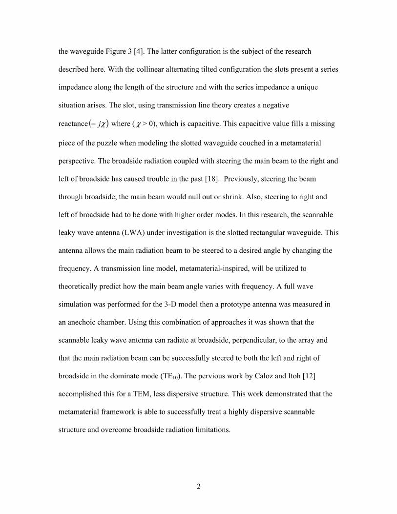
the waveguide Figure 3 [4]. The latter configuration is the subject of the research
described here. With the collinear alternating tilted configuration the slots present a series
impedance along the length of the structure and with the series impedance a unique
situation arises. The slot, using transmission line theory creates a negative
reactance ( )χj− where ( χ > 0), which is capacitive. This capacitive value fills a missing
piece of the puzzle when modeling the slotted waveguide couched in a metamaterial
perspective. The broadside radiation coupled with steering the main beam to the right and
left of broadside has caused trouble in the past [18]. Previously, steering the beam
through broadside, the main beam would null out or shrink. Also, steering to right and
left of broadside had to be done with higher order modes. In this research, the scannable
leaky wave antenna (LWA) under investigation is the slotted rectangular waveguide. This
antenna allows the main radiation beam to be steered to a desired angle by changing the
frequency. A transmission line model, metamaterial-inspired, will be utilized to
theoretically predict how the main beam angle varies with frequency. A full wave
simulation was performed for the 3-D model then a prototype antenna was measured in
an anechoic chamber. Using this combination of approaches it was shown that the
scannable leaky wave antenna can radiate at broadside, perpendicular, to the array and
that the main radiation beam can be successfully steered to both the left and right of
broadside in the dominate mode (TE10). The pervious work by Caloz and Itoh [12]
accomplished this for a TEM, less dispersive structure. This work demonstrated that the
metamaterial framework is able to successfully treat a highly dispersive scannable
structure and overcome broadside radiation limitations.

3
Figure 1: Longitudinal Slotted Rectangular Waveguide, Top View
Figure 2: 2-D Longitudinal Slotted Planar Array, Top View
Figure 3: Tilted Slot Rectangular Waveguide, Top View
2.0 Waveguide Impedance/Admittance Derivation
The metamaterial inspired transmission line modeling has four components: two
capacitive elements and two inductive elements, this is explained later in the thesis. The
waveguide contributes three of the four elements in the transmission line modeling, two
inductive and one capacitive; the other capacitive element is from the slot. It is shown
below how waveguide portion is derived. From two of Maxwell’s Equations,
( HjE ωμ−=×∇ ) and ( EjH ωε=×∇ ) you can get the following for the loss-free region
within the waveguide, ( )ω is angular frequency [19, 20].

4
xyz EjH
yH ωεγ =+∂
∂ (a)
yxz EjH
xH ωεγ −=+∂
∂ (b)
zxy Ej
yH
xH
ωε=∂
∂−
∂∂
(c) (1)
xyz HjE
yE ωμγ −=+∂
∂ (d)
yxz HjE
xE ωμγ =+∂
∂ (e)
zxy Hj
yE
xE
ωμ−=∂
∂−
∂∂
f)
βαγ j+=
Figure 4: Waveguide Coordinate System The above equations can be solved for four transverse equations in terms of ( zE ) and
( zH ) [21].

5
⎟⎟⎠
⎞⎜⎜⎝
⎛∂
∂−
∂∂
=x
Hy
EkjH zz
cx βωε2 (a)
⎟⎟⎠
⎞⎜⎜⎝
⎛∂
∂+
∂∂−=
yH
xE
kjH zz
cy βωε2 (b)
(2)
⎟⎟⎠
⎞⎜⎜⎝
⎛∂
∂+
∂∂−=
yH
xE
kjE zz
cx ωμβ2 (c)
⎟⎟⎠
⎞⎜⎜⎝
⎛∂
∂+
∂∂
−=x
Hy
EkjE zz
cy ωμβ2 (d)
222 β−= kkc , λπ2=k ,
gλπβ 2= , roεεε = , ro μμμ = , and fπω 2=
(kc) is the cutoff wavenumber, (k) is the free space wavenumber, (β) is the propagation
constant, (ε) is the permittivity with (εo) being permittivity of free space and (εr) being the
relative permittivity, (μ) is the permeability with (μo) being the permeability of free space
and (μr) being the relative permeability, and (ω) is the angular frequency with ( f) being
the frequency of interest.
In the longitudinal direction of propagation for the TE-mode (Ez = 0) and (Hz ≠ 0). With
this, the above equations reduce to the following.

6
xH
kjH z
cx ∂
∂−= 2
β (a)
y
Hk
jH z
cy ∂
∂−= 2
β (b) (3)
yH
kjE z
cx ∂
∂−= 2
ωμ (c)
xH
kjE z
cy ∂
∂−= 2
ωμ (d)
Now dividing the E-field by the H-field for the characteristic wave impedance of the TE-
mode (ZoTE):
γμωj
HE
HE
Zx
y
y
xTEo =
−== (4)
With this said the transmission line analogy for a waveguide can be shown using
rectangular coordinate field equations.

7
xyz Ej
zH
yH ωε=
∂∂
−∂
∂ (a)
yzx Ej
xH
zH ωε=
∂∂
−∂
∂− (b)
zxy Ej
yH
xH
ωε=∂
∂−
∂∂
(c) (5)
xyz Hj
zE
yE ωμ−=
∂∂
−∂
∂ (d)
yzx Hj
xE
zE ωμ−=
∂∂
−∂
∂ (e)
zxy Hj
yE
xE
ωμ−=∂
∂−
∂∂
(f)
From (5) we are interested in (5a) and (5d). Since ( 0=zE ) and ( 0=Hcurlxy ) it is
possible to define a magnetic scalar potential (U):
xUH x ∂
∂−= yUH y ∂
∂−=
Now using (U), and (5a), (5d), and (2) we will get the following.
xUj
xH
kj
zz
c ∂∂−=⎟⎟
⎠
⎞⎜⎜⎝
⎛
∂∂
∂∂ ωμωμ
2 y
Hkz
Hy
H z
c
yz
∂∂
=∂
∂−
∂∂
2
2μεω
Therefore
UjHkj
z zc
ωμωμ −=⎟⎟⎠
⎞⎜⎜⎝
⎛
∂∂
2 ⎟⎟⎠
⎞⎜⎜⎝
⎛⎟⎟⎠
⎞⎜⎜⎝
⎛+−=
∂∂
zc
c Hkjj
jk
zU
2
2 ωμωεωμ

8
The quantity ⎟⎟⎠
⎞⎜⎜⎝
⎛z
c
Hkj
2
ωμ has voltage dimensions and (U) has current dimensions.
The waveguide series impedance [20]:
ωμωμ jZjZIVZZI
zV =⇒−=−⇒=−⇒−=
∂∂ (6)
The waveguide shunt admittance [20]:
⎟⎟⎠
⎞⎜⎜⎝
⎛+=⇒⎟
⎟⎠
⎞⎜⎜⎝
⎛+−=−⇒=−⇒−=
∂∂ ωε
ωμωε
ωμj
jk
Yjjk
YVIYYV
zI cc
22
(7)
There is a useful relationship between the constitutive parameters ( )εμ and per unit
length parameters ( )LC ′′ [22]:
( ) ( )εμ=′′LC (8)
2.1 TE Mode Equivalent Circuit Model
Below is a TE mode equivalent circuit flow chart of how a section of waveguide is
represented with a complex series impedance and shunt admittance per unit length. The
sinusoidal wave indicates the direction of propagation in the waveguide. The ( )Z ′ , ( )Y ′ ,
( )C ′ , and ( )L′ are per unit length values.
Figure 5: Physical Waveguide to Block Diagram
9
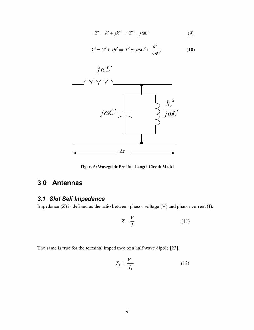
LjZXjRZ ′=′⇒′+′=′ ω (9)
Lj
kCjYBjGY c
′+′=′⇒′+′=′
ωω
2
(10)
Figure 6: Waveguide Per Unit Length Circuit Model
3.0 Antennas
3.1 Slot Self Impedance Impedance (Z) is defined as the ratio between phasor voltage (V) and phasor current (I).
IVZ = (11)
The same is true for the terminal impedance of a half wave dipole [23].
1
1111 I
VZ = (12)
zΔ
Cj ′ω
Lj ′ω
Ljkc
′ω
2

10
According to John D. Kraus [23] § 10.3 there is a good derivation using the Sine and
Cosine Integrals where the dipole impedance becomes complex with a real and imaginary
(inductive) part:
jXRZ += (13)
with
)2(30 πCinR = (14)
)2(30 πSiX = (15)
where Ci(x) = Cosine Integral, n = odd number multiple, and Si(x) = Sine Integral. The
cosine and sine integrals are defined mathematically as [23]:
( ) ( )∫∞=
xdv
vvxCi cos (16)
( ) ( )dvv
vxSix
∫=0
sin (17)
The above impedance value is for non-resonant antennas. Resonant antennas just have a
real (R) part. Then, H.G Booker used Babinet’s Principle (optics) in electromagnetics to
relate the known impedance of a dipole antenna to calculate the impedance of a
complementary slot [24]:
4
2η=sd ZZ (18)
11
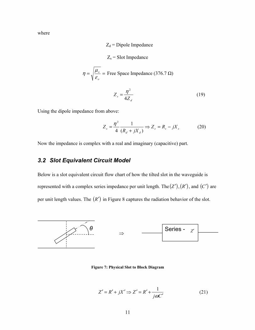
where
Zd = Dipole Impedance
Zs = Slot Impedance
==o
o
εμη Free Space Impedance (376.7 Ω)
d
s ZZ
4
2η= (19)
Using the dipole impedance from above:
sssdd
s jXRZjXR
Z −=⇒+
=)(
14
2η (20)
Now the impedance is complex with a real and imaginary (capacitive) part.
3.2 Slot Equivalent Circuit Model
Below is a slot equivalent circuit flow chart of how the tilted slot in the waveguide is
represented with a complex series impedance per unit length. The ( )Z ′ , ( )R′ , and ( )C ′ are
per unit length values. The ( )R′ in Figure 8 captures the radiation behavior of the slot.
Figure 7: Physical Slot to Block Diagram
Cj
RZXjRZ′
+′=′⇒′+′=′ω1 (21)
θ ⇒
Series - Z′

12
Figure 8: Slot Per Unit Length Circuit Model
3.3 Mutual Impedance
When dealing with more than one radiator, mutual impedance has to be taken into
account.
j
iij I
VZ = (22)
This means the total impedance (ZTi) of one radiator is dependant on the other radiators.
In Figure 9 there is a linear array of three slots and using the (NxN) matrix, (23), for a
three port network the total impedance of each slot can be found.
1 2 31 2 3
Figure 9: Three Slot Linear Array
per slot
R′ Cj ′ω1

13
⎥⎥⎥
⎦
⎤
⎢⎢⎢
⎣
⎡
⎥⎥⎥
⎦
⎤
⎢⎢⎢
⎣
⎡=
⎥⎥⎥
⎦
⎤
⎢⎢⎢
⎣
⎡
3
2
1
333231
232221
131211
3
2
1
III
ZZZZZZZZZ
VVV
(23)
Distributing the current using matrix algebra for the first slot in the array, the voltage will
be:
Now divide both sides by the current of the first slot (I1) to get the total impedance of the
slot.
(24)
Without including the mutual impedance from the other slots will result in, an incorrect
total slot impedance. Doing this for the rest of the slots will result in the following
equations.
⇒
⇒
The LWA used in this thesis has ten slots down the center of the waveguide with a tilt.
This may be referred to as coplanar skewed slots. In a center line configuration of series
slots, the angle (±θ), in Figure 10, from horizontal has to be greater than (0 degrees) in
order to interrupt the longitudinal current flow in the top broadwall of the waveguide to
1
313
1
21211
1
11 I
IZIIZZ
IVZT ++==
3132121111 IZIZIZV ++=
3232221212 IZIZIZV ++=2
32322
2
121
2
22 I
IZZIIZ
IVZT ++==
3332321313 IZIZIZV ++= 333
232
3
131
3
33 Z
IIZ
IIZ
IVZT ++==
14
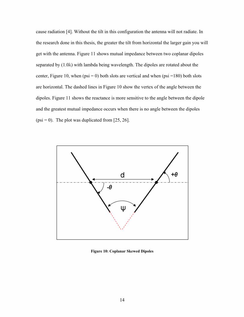
cause radiation [4]. Without the tilt in this configuration the antenna will not radiate. In
the research done in this thesis, the greater the tilt from horizontal the larger gain you will
get with the antenna. Figure 11 shows mutual impedance between two coplanar dipoles
separated by (1.0λ) with lambda being wavelength. The dipoles are rotated about the
center, Figure 10, when (psi = 0) both slots are vertical and when (psi =180) both slots
are horizontal. The dashed lines in Figure 10 show the vertex of the angle between the
dipoles. Figure 11 shows the reactance is more sensitive to the angle between the dipole
and the greatest mutual impedance occurs when there is no angle between the dipoles
(psi = 0). The plot was duplicated from [25, 26].
Figure 10: Coplanar Skewed Dipoles

15
Figure 11: Mutual Impedance between Coplanar Skewed Dipoles
4.0 Metamaterials
Metamaterials is a relatively new area of research in electromagnetics/antennas.
Figure 12 shows an ideal lossless cell from a multi-cell metamaterial transmission line
model. This model has series impedance (Z) and shunt admittance (Y) per unit cell.
Using the model inspired by a metamaterial modeling approach applied to the LWA, it
can be shown the main beam radiation is accurately predicted.

16
CL LR
LLCR
Z
Y
p
CL LR
LLCR
Z
Y
p
Figure 12: Ideal Metamaterial Transmission Line Model
4.1 LC Parameter Extraction
The LC parameter extraction is an approach to evaluate the series/shunt inductances (L)
and capacitances (C) for the transmission line model. This approach allows a design to be
predicted without creating the entire structure. The idea is to the predict radiation angle of
the main beam of the radiating structure by extracting the capacitances and inductances
of one cell of the structure. This approach stems from work published by Caloz, Atsushi,
and Itoh who used it to extract the right handed capacitance (CR), right handed inductance
(LR), left handed capacitance (CL), and left handed inductance (LL) for a transverse
electromagnetic (TEM) structure [11]. The structure they used was a microstrip antenna
which is a transverse electromagnetic (TEM) mode, two conductor, ground plane and top
structure separated by a dielectric [11]. A similar approach is used in this research to treat
a more dispersive transmission structure.

17
The LC Parameter Extraction approach:
• Have the initial design and run physical components of the cell model in a full
wave simulator to evaluate the scattering parameters (S-parameters).
• Convert the S-parameters to impedance parameters (Z-parameters) or admittance
parameters (Y-parameters).
• Solve for each of the right/left handed L’s and C’s.
• Use the right/left handed L’s and C’s to determine the phase constant (β).
• Place (β) in the main beam angle equation.
The approach was employed in this research to extract the L’s and C’s for the LWA. The
LWA, tilted slot rectangular waveguide, under investigation is a dispersive radiating
structure. In order to get the impedance parameters first the design has to be broken into
the components of the cell and predicted separately, the waveguide section is predicted
separate from the slot and vice versa. Figure 13 is the half wavelength waveguide section
that was run in the full wave simulator to get the S-parameters for the waveguide portion
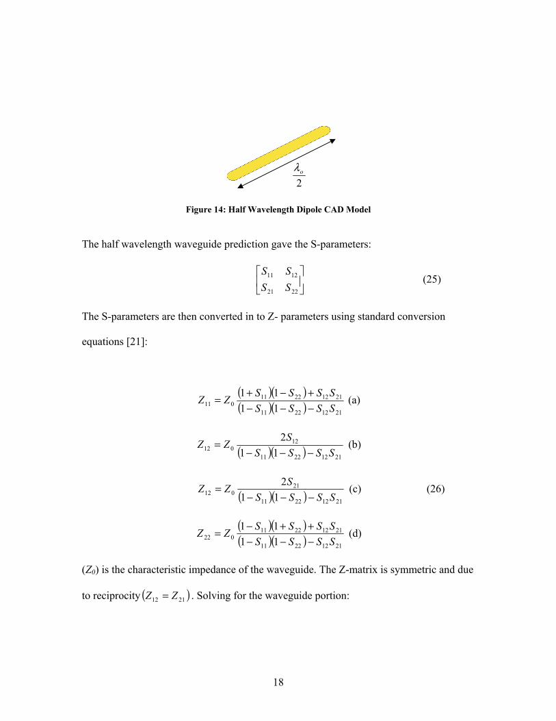
of the model. Figure 14 is the half wavelength dipole that was evaluated in the full wave
simulator to get the impedance values for the slot portion of the model.
Figure 13: Half Wavelength Waveguide Section CAD Model
2oλ
18
Figure 14: Half Wavelength Dipole CAD Model
The half wavelength waveguide prediction gave the S-parameters:
⎥⎦
⎤⎢⎣
⎡
2221
1211
SSSS
(25)
The S-parameters are then converted in to Z- parameters using standard conversion
equations [21]:
( )( )( )( ) 21122211
21122211011 11
11SSSSSSSS
ZZ−−−+−+
= (a)
( )( ) 21122211
12012 11
2SSSS
SZZ
−−−= (b)
( )( ) 21122211
21012 11
2SSSS
SZZ
−−−= (c) (26)
( )( )( )( ) 21122211
21122211022 11
11SSSSSSSS
ZZ−−−++−
= (d)
(Z0) is the characteristic impedance of the waveguide. The Z-matrix is symmetric and due
to reciprocity ( )2112 ZZ = . Solving for the waveguide portion:
2oλ

19
SWGZ
PWGY
SWGLjω
PWG
c
Ljk
ω
2P
WGCjω
SWGZ
PWGY
SWGLjω
PWG
c
Ljk
ω
2P
WGCjω
Figure 15: Waveguide Cell Circuit Equivalent Model
S
WGSWG LjZ ω= (27)
PWG
cPWG
PWG Lj
kCjY
ωω
2
+= (28)
The half wavelength dipole’s prediction gave the impedance value which is converted to
a slot impedance value by using the Babinet-Booker Principle mentioned above. The slot
impedance has a real component in it however; the real part can be neglected for the
phase calculation (β).
Figure 16: Slot Cell Circuit Equivalent Model
SSlotZ
SSlotCjω
1

20
SSlot
SSlot Cj
Zω
1= (29)
The Z- parameters for the waveguide are:
⎥⎥⎥⎥
⎦
⎤
⎢⎢⎢⎢
⎣
⎡
+−
−+=⎥
⎦
⎤⎢⎣
⎡=
SWGP
WGP
WG
PWG
SWGP
WGWGWG
WGWG
WG
ZYY
YZ
YZZZZ
Z 11
11
2221
1211 (30)
SWGZ S
WGZ
PWGY
SWGZ S
WGZ
PWGY
Figure 17: T-Network
The negative sign for ( )WGZ12 and ( )WGZ 21 in (30) conforms to the convention of having the
current coming into either side of two port network as shown in Figure 18 [27].
Figure 18: Block Diagram of a Two-Port Network

21
The Z-parameter for the slot is:
SSlot
SlotSlot ZZZ == 11 (31)
Each of the inductances and capacitances in (27, 28, and 29) are:
( )12112 ZZj
LSWG −=
ω (32)
112
1Zj
C SSlot ω
= (33)
⎟⎟⎠
⎞⎜⎜⎝
⎛−= P
WG
cPWG Lj
kY
jC
ωω
21 (34)
⎟⎟⎠
⎞⎜⎜⎝
⎛−
= PWG
cPWG CjY
kj
Lωω
21 (35)
In order to solve for the parallel capacitance and inductance see Figure 15, the partial
derivative of ( )PWGY is taken with respect to angular frequency ( )ω :
0=⎟⎟⎠
⎞⎜⎜⎝
⎛∂
∂ω
PWGY
(36)

22
This is done to create a second equation in order to solve for each variable. Once the
partial derivative is taken, it is set equal to zero and solved, for either the capacitance or
inductance. The right/left hand L’s and C’s for the metamaterials model are shown
below.
Series Impedance:
SlotSSlotL Zj
CC112
1ω
== (37)
( )WGWGSWGR ZZ
jLL 1211
2 −==ω
(38)
The “2” in the denominator of (37) and the numerator of (38) results from representing
these elements as a T-network that combines properly with elements adjacent in the
metamaterials transmission line model Figure 19.
Figure 19: T-Network Model
23
Shunt Admittance:
ω2j
YCC
PWGP
WGR == (39)
PWG
cPWGL Yj
kLL
ω
22== (40)
The LC extracted parameters are: LL = 6.683 nH, CL = 0.149 pF, LR = -12.886 μH, and
CR = -0.349 pF. These four variables LL, CL, LR, and CR, are used to calculate the phase
constant (β) with the following equation [11]:
( ) ⎟⎟⎠
⎞⎜⎜⎝
⎛−=
LLRR CL
CLp ω
ωωβ 11 (41)
( )p is the physical cell size. Once (β) is known for each of the different frequencies, it
can be substituted in the following equation to determine the main beam angle (θMB) for
an alternating titled slot LWA [5, 11].
⎟⎠⎞
⎜⎝⎛ −= −
dkMB 2cos 1 λβθ (42)
(42) is the ( )ψpsi variable from array theory, which is used in many variations of the
array factor (AF) equation [28, 29].
24
( )∑=
−=N
n
njeAF1
1 ψ (43)
where
ddko βθψ −= )cos( (44)
For the tilted slot rectangular waveguide array case it is [28]:
ππβθ mddko 2)cos( =+− ; ( )...3,2,1,0=m (45)
Here ⎟⎟⎠
⎞⎜⎜⎝
⎛=
ook
λπ2 , d is the inter-element slot spacing, β is given by (41), and θ is solved
for, ( )MBθθ = for (42) and (45). The addition of ( )π accounts for the possible (180o)
phase change due to the tilt of the slot [4, 28]. The calculation from (42) is only accurate
if there is negligible mutual coupling between the slots in the array [4, 29]. Using the
dispersive tilted slot rectangular waveguide this is not the case as the LC parameter
extraction predicted results will show.
5.0 Antenna Model
The full wave simulator used to predict the main beam angle (θMB) for the LWA is (In-
situ Large ANtenna Aperture & Array Simulations) (Code for the Analysis of Radiators
on LOssy Surfaces) (ILANS CARLOS). CARLOS implements the method of moments
(MoM) analysis technique. This analysis will give the solution for a fully arbitrary three
dimensional (3-D) complex radiator. The solutions are obtained for perfectly conducting
bodies (PEC) as well as partially penetrable ones. The electromagnetic solution is based
25
on the electric field integral equation (EFIE). CARLOS uses planar triangular patch
representation for all of the surfaces and boundaries of the radiator [30].
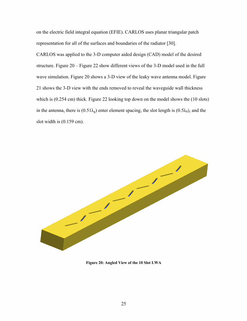
CARLOS was applied to the 3-D computer aided design (CAD) model of the desired
structure. Figure 20 – Figure 22 show different views of the 3-D model used in the full
wave simulation. Figure 20 shows a 3-D view of the leaky wave antenna model. Figure
21 shows the 3-D view with the ends removed to reveal the waveguide wall thickness
which is (0.254 cm) thick. Figure 22 looking top down on the model shows the (10 slots)
in the antenna, there is (0.51λg) enter element spacing, the slot length is (0.5λ0), and the
slot width is (0.159 cm).
Figure 20: Angled View of the 10 Slot LWA

26
Figure 21: Cross Section of the LWA Looking Down the Waveguide
Figure 22: Top Down View of the LWA
After the structure is designed in the CAD environment it must be sub-divided into
surface facets. This means the structure is broken into small triangular segments in order
to calculate the currents on the surface. Once the interactions between each of the facets
are known the currents are determined and the ( )fieldE −r
and ( )fieldH −r
for the
problem can be solved. Figure 23 and Figure 24 shows the faceted model used in the
simulation. Notice the grid is finer around each of the slots; this is to capture the detail of
the slot. For example there are ten facets at each end of each slot to reveal the rounded
slot ends. Figure 23 shows the facetized model with (104661 unknowns) and the grid
density is (λ/20). Figure 24 shows a close-up view of a slot and the grid density. The blue
outline helps identify the slot edges in the grid.
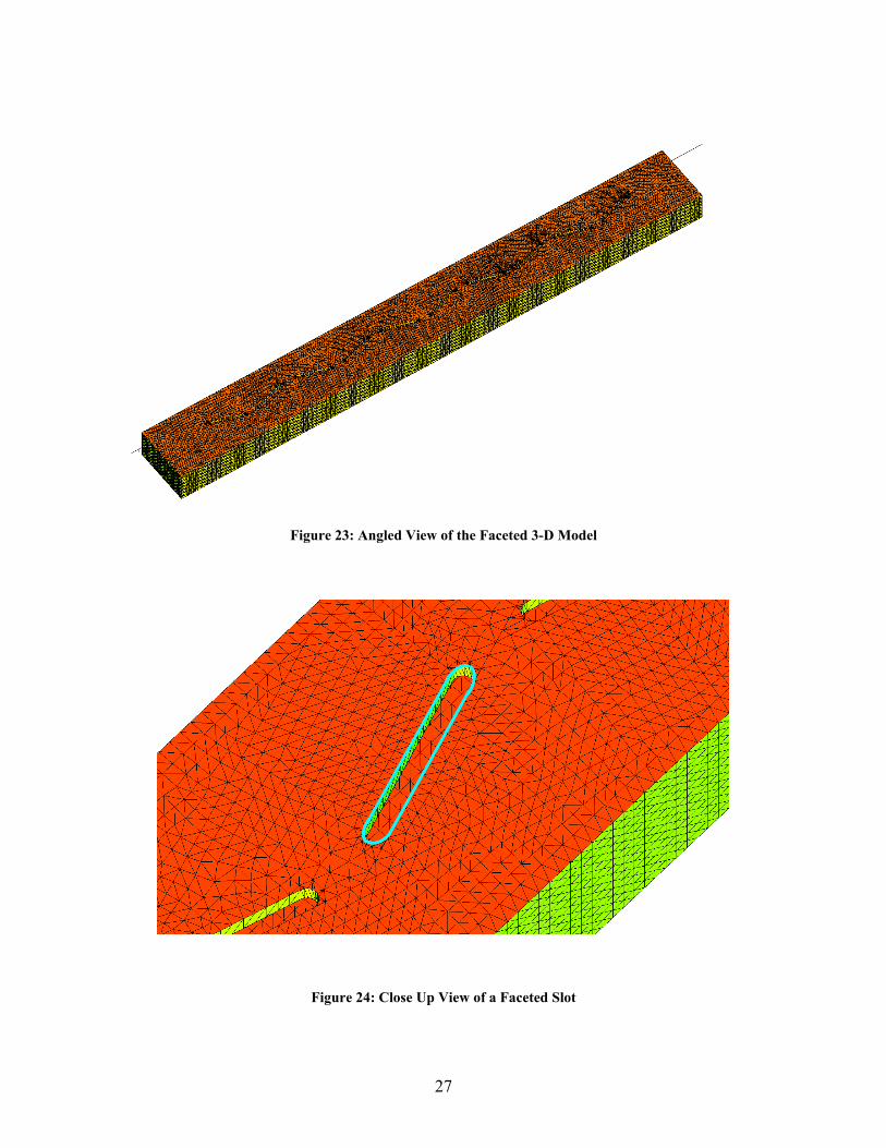
27
Figure 23: Angled View of the Faceted 3-D Model
Figure 24: Close Up View of a Faceted Slot

28
Figure 25 shows the excitation of the LWA. This figure shows the TE10 mode in the
waveguide and also shows the slots being excited. The subscripts in (TEmn) are the
number of half cycles of the propagating mode. The (m) is the number of half cycles in
the x-direction and (n) is the number of half cycles in the y-direction. To show the range
of excitation the dark blue shows no excitation and the red is peak excitation.
Figure 25: Angled Waveguide View
Figure 26 is a cross section looking down the LWA. Here the color presentation shows
TE10 mode clearly dies off at the sidewalls and peaks in the middle. This view also shows
the closed region of the model, the dark blue perimeter. At the top of the TE10 mode are
the excited slot walls.
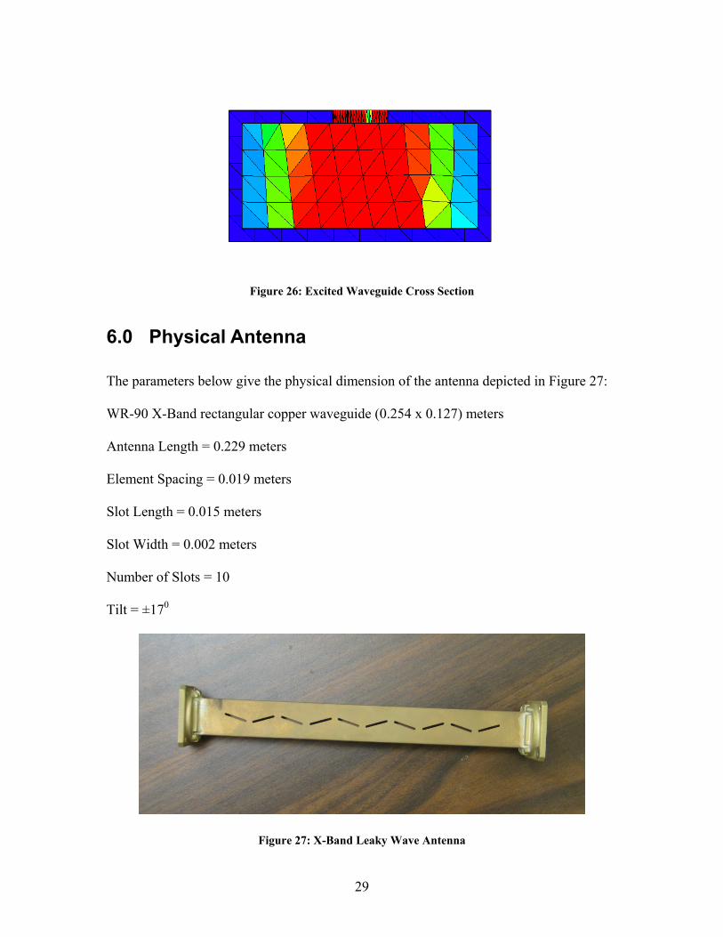
29
Figure 26: Excited Waveguide Cross Section
6.0 Physical Antenna
The parameters below give the physical dimension of the antenna depicted in Figure 27:
WR-90 X-Band rectangular copper waveguide (0.254 x 0.127) meters
Antenna Length = 0.229 meters
Element Spacing = 0.019 meters
Slot Length = 0.015 meters
Slot Width = 0.002 meters
Number of Slots = 10
Tilt = ±170
Figure 27: X-Band Leaky Wave Antenna

30
In Figure 28 the antenna has attachments at both ends. The gray box on the left end of the
LWA is the probe feed excitation for the antenna. There is a probe located at the bottom
of the small gray box and launches the wave in the guide. The antenna was excited with a
TE10 mode this is the fundamental mode for the waveguide. The copper section between
the excitation and the antenna is a spacer to position the excitation in the anechoic
chamber on the pole. At the other end of the antenna is a blue rectangular box which is
the load, this is a match load for the X-Band (TE10) mode and does not allow any
reflections in the antenna.
Figure 28: Leaky Wave Antenna with Excitation and Matched Load
Figure 29 is the antenna mounted in the anechoic chamber on the positioner pole. The
positioner moves in both theta and phi directions. The blueish box with the circular disk
allows the phi-direction movement. The box itself is seen in the measurements for the
different frequencies, this will be discussed later.

31
Figure 29: Leaky Wave Antenna Mounted on the Positioner Pole
6.1 Test Setup
The measurements of the antenna were taken in an anechoic chamber. Figure 30 is a
block diagram of the test setup. The transmitter (TX) is a Scientific Atlanta Standard
Gain Horn Model 12 - 8.20, Frequency Range (8.2 - 12.4 GHz) and the receiver (RX) is
the leaky wave antenna. The measurement system controller is a desktop PC which
collects the measurement data. The network analyzer is an Agilent Technologies E8363B
10MHz - 40GHz, PNA Series Network Analyzer.

32
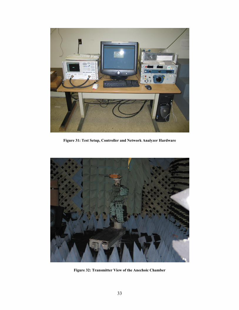
Figure 30: Test Setup Block Diagram
The objects in Figure 31 are the network analyzer on the left, the Measurement System
Controller monitor in the middle, and the Positioner Control on the right.
Figure 32 is looking into the anechoic chamber from the transmitting horn antenna
position. The positioner in the chamber spins on an imaginary axis from the floor to the
ceiling allowing the theta angles in the measurements. The measurements taken in this
research hold the phi positioner constant while the theta positioner varies. Figure 33 is
looking at the transmitting antenna from the positioner.
RX
Positioner
Network Analyzer
Measurement System
Controller
Positioner Control
Theta/Phi
TX
33
Figure 31: Test Setup, Controller and Network Analyzer Hardware
Figure 32: Transmitter View of the Anechoic Chamber

34
Figure 33: Receiver View of the Anechoic Chamber
6.2 Full Wave Simulation and Measured Results
The following radiation gain patterns are the full wave simulator (predicted) data using
CARLOS and the measured data from the test setup mentioned above. The patterns are
far field conic cuts with a constant phi of (270 degrees) and a varying theta
(0 – 360 degrees). The plots are normalized to peak gain. Figure 34 is the coordinate
system used for the data.

35
Figure 34: Predicted/Measured Coordinate System
6.3 Backlobes
The leaky wave antenna’s predicted and measured data shown below are not predicted or
measured with an infinite ground plane. With this said, the finite length of the broadwall,
where the slots are, of the antenna (2.54 cm) has some effects that would not be there if it
were possible to have an infinite ground plane behind the antenna during data collection.
The effects are backlobes. The currents that are induced on the broadwall during radiation
travel along the surface. When those currents reach the edge of the surface they will
radiate and diffract around the edge of the surface and radiate in a different direction.
With this diffraction you will get backlobes. The diffraction can be explained by
Geometric Theory of Diffraction (GTD) [29, 31]. Figure 35 shows the edge diffraction
from a finite surface mounted on the end of a truncated rectangular waveguide [31].
2700
1800
00 Phi900
00 Theta
900
2700

36
Figure 35: E- and H-plane Diffraction by a Rectangular Waveguide. Figure Copied From [31 pg. 808])
6.3.1 8.3 GHz Data
The data taken for (8.3 GHz) is in good agreement for the predicted and measured results,
the main beam peak points to (190) for the predicted and (18.880) for the measured. The
figures below are the far patterns, Figure 36 is the predicted pattern and Figure 37 is the
measured pattern. Figure 38 is the predicted and measured combined patterns.
Figure 36 Figure 37
These are the (8.3 GHz) predicted data Figure 36 and measured data Figure 37
normalized gain plots, with a constant azimuth (270o) and varying elevation.

37
Figure 38: (8.3 GHz) Combined Normalized Gain Plot, With a Constant Azimuth (270o) and Varying Elevation
6.3.2 9.3 GHz Data
The data taken for (9.3 GHz) is in good agreement for the predicted and measured results,
the main beam peak points to (70) for the predicted and (8.250) for the measured. The
figures below are the far patterns, Figure 39 is the predicted pattern and Figure 40 is the
measured pattern. Figure 41 is the predicted and measured combined patterns.
38
Figure 39 Figure 40
These are the (9.3 GHz) predicted data Figure 39 and measured data Figure 40
normalized gain plots, with a constant azimuth (270o) and varying elevation.
Figure 41: (9.3 GHz) Combined Normalized Gain Plot, With a Constant Azimuth (270o) and Varying Elevation

39
6.3.3 10.3 GHz Data
The data taken for (10.3 GHz) is in good agreement for the predicted and measured
results, the main beam peak points to (359.00) for the predicted and (360.00) for the
measured. The figures below are the far patterns, Figure 42 is the predicted pattern and
Figure 43 is the measured pattern. Figure 44 is the predicted and measured combined
patterns. Notice the backlobe pointing at (1800) for the predicted data and see that it is not
there for the measured data. This is due to mounting the antenna in front of the phi
rotator, Figure 29, and the backlobe diffracting around the rotator and splitting into two
backlobes at (~1550) and (~2050).
Figure 42 Figure 43
These are the (10.3 GHz) predicted data Figure 42 and measured data Figure 43
normalized gain plots, with a constant azimuth (270o) and varying elevation.

40
Figure 44: (10.3 GHz) Combined Normalized Gain Plot, With a Constant Azimuth (270o) and Varying Elevation
6.3.4 11.3 GHz Data
The data taken for (11.3 GHz) is in good agreement for the predicted and measured
results, the main beam peak points to (353.00) for the predicted and (354.00) for the
measured. The figures below are the far patterns, Figure 45 is the predicted pattern and
Figure 46 is the measured pattern. Figure 47 is the predicted and measured combined
patterns.
41
Figure 45 Figure 46
These are the (11.3 GHz) predicted data Figure 45 and measured data Figure 46
normalized gain plots, with a constant azimuth (270o) and varying elevation.
Figure 47: (11.3 GHz) Combined Normalized Gain Plot, With a Constant Azimuth (270o) and Varying Elevation

42
6.3.5 12.3 GHz Data
The data taken for (12.3 GHz) is in good agreement for the predicted and measured
results, the main beam peak points to (348.00) for the predicted and (348.370) for the
measured. The figures below are the far patterns, Figure 48 is the predicted pattern and
Figure 49 is the measured pattern. Figure 50 is the predicted and measured combined
patterns.
Figure 48 Figure 49
These are the (12.3 GHz) predicted data Figure 48 and measured data Figure 49
normalized gain plots, with a constant azimuth (270o) and varying elevation
43
Figure 50: (12.3 GHz) Combined Normalized Gain Plot, With a Constant Azimuth (270o) and Varying Elevation
6.3.6 LC Parameter Extraction Prediction Results
The main beam angle (θMB) predictions are in Table 1. The polar plot in Figure 51 shows
(900) at broadside, endfire to the right of broadside, and backfire to the left of broadside.
The LWA’s fundamental frequency (f0) is (10.3 GHz) and the table below shows it is not
at broadside. None of the predictions in Table 1 below or on the polar plot in Figure 51
show the correct predicted main beam angle. If the predictions were correct, then the
frequencies (8.3 GHz and 9.3 GHz) would be to the left of broadside, backfire, and the
frequencies (11.3 GHz and 12.3 GHz) would be to the right of broadside, endfire. The
suspected reason for the incorrect predictions is the lack of mutual coupling in the
prediction equations. Another possible explanation for the LC parameter extraction

44
predictions being incorrect is the application of the Babinet-Booker Principle in
determining the slot impedance.
Frequency 8.3 GHz 9.3 GHz 10.3 GHz 11.3 GHz 12.3 GHz
Angle (degree) 86.964 81.088 76.292 72.275 68.844
Table 1: LC Parameter Extraction Main Beam Predictions
Figure 51: LC Parameter Predictions on a Polar Plot
7.0 Conclusion
In this research there are three different approaches in determining the main beam
angle ( )MBθ . The first approach used the metamaterial LC parameter extraction developed
by C. Caloz and T. Itoh. The second approach was a full wave 3-D simulation using
CARLOS and the third was a prototype that was measured. The LC parameter extraction
did not work in this case due to the mutual coupling that takes place with tilted slot leaky

45
wave antenna, or possibly due to the Babinet-Booker Principal as mentioned previously.
If the LC parameter extraction approach would have worked it would have let the
designer design a portion of the radiating structure by using the parameters extracted
from the single unit cell: CL, LL, CR, and LL. The full wave simulator approach and
prototype antenna did have good agreement. The results show that tilted slot leaky wave
antenna can radiate at broadside and move through both the right and left of broadside at
the dominate mode (TE10) by scanning the frequency. The radiation patterns show a
relative narrow beam and the measured data shows the physical interaction between the
antenna and the mounting pole, unlike the ideal conditions in the full wave simulator.
8.0 Future Work
There remains an opportunity for continued work on this problem. The mutual coupling
needs to be accounted for in calculating the main beam pointing angle ( )MBθ . This would
give greater insight in the type of radiating element that may be used on a given antenna
by showing how the elements interact with each other. This would also allow a wider
range of radiating structures to use (42) in determining main beam radiation angles. Other
future work is determining if the Babinet-Booker Principle was applied correctly.

46
Bibliography
1. Watson, W. H. "The Physical Principles of Waveguide Transmission and Antenna
Systems," Oxford University Press, New York, 1947.
2. Oliner, A. A. “The Impedance Properties of Narrow Radiating Slots in the Broad
Face of Rectangular Waveguide. Part I – Theory.” IRE Transactions on Antennas
and Propagation Jan., 1957.
3. Oliner, A. A. “The Impedance Properties of Narrow Radiating Slots in the Broad
Face of Rectangular Waveguide. Part II– Comparison with Measurements.” IRE
Transactions on Antennas and Propagation Jan., 1957.
4. Ramsay, J. F., Popovich, B. V. “Series-Slotted Waveguide Array Antennas.”
Cutler-Hammer, Inc., Deer Park, NY, USA. IRE International Convention Record
Vol. 11, pg. 30-55, Mar. 1963.
5. Elliott, R. S. Antenna Theory and Design. Englewood Cliffs, New Jersey:
Prentice-Hall, Inc, 1981.
6. Veselago, V. “The electrodynamics of substances with simultaneously negative
values of ε and μ,” Soviet Physics Uspekhi, vol. 10, no. 4, pp. 509–514, 1968.
7. Pendry, J.B. “Negative refraction makes a perfect lens,” Phys. Rev. Lett., vol. 85,
pp. 3966–3969, Oct. 2000.
8. Shelby, R.A., Smith, D.R. and Schultz, S. “Experimental verification of a
negative index of refraction,” Science, vol. 292, no. 5514, pp. 77–79, 2001.
9. Eleftheriades, G. V., Siddiqui, O. and Iyer, A.K. “Transmission line models for
negative refractive index media and associated implementations without excess

47
resonators,” IEEE Microwave Wireless Compon. Lett., vol. 13, pp. 51–53, Feb.
2003.
10. Oliner, A. A., “A Periodic-Structure Negative-Refraction-Index Medium without
Resonant Elements”. IEEE-AP-S Digest, San Antonio, TX p. 41. 2002.
11. Caloz, C., and Itoh, T. Electromagnetic Metamaterials: Transmission Line Theory
and Microwave Applications. Hoboken, New Jersey: John Wiley & Sons, Inc.
2006.
12. Caloz, C., Sanada, A., and Itoh, T. “A Novel Right/Left-Handed Coupled-Line
Directional Coupler with Arbitrary Coupling Level and Broad Bandwidth.” IEEE
Transactions on Microwave Theory and Techniques Vol. 52, No. 3, March 2004.
13. Caloz, C. and Itoh, T. “Transmission Line Approach of Left-Handed (LH)
Materials and Microstrip Implementation of an Artificial LH Transmission Line.”
IEEE Transactions on Antennas and Propagation Vol. 52, No. 5, May, 2004.
14. Liu, L., Caloz, C., and Itoh, T. “Dominant Mode Leaky Wave Antenna with
Backfire-to-Endfire Scanning Capability.” Electronic Letters Vol. 38, No. 23,
Nov. 7th, 2002.
15. Caloz, C. and Itoh, T. “Invited – Novel Microwave Devices and Structures on the
Transmission Line Approach of Meta-Materials.” IEEE MTT-S Digest, 2003.
16. Lai, A., Caloz, C., and Itoh, T. “Composite Right/Left-Handed Transmission Line
Metamaterials.” IEEE Microwave Magazine Sept. 2004.
17. Caloz, C., Itoh, T., and Rennings, A. “CRLH Metamaterial Leaky-Wave and
Resonant Antennas.” IEEE Transactions on Antennas and Propagation Vol. 50,
No. 5, October, 2008.

48
18. Johnson, R. C. Antenna Engineering Handbook 3rd Edition. New York: McGraw-
Hill, 1993.
19. Harrington, R. F. Time-Harmonic Electromagnetic Fields. New York: McGraw-
Hill, 1961.
20. Jordan, E. C. Electromagnetic Waves and Radiating Systems. Englewood Cliffs,
New Jersey: Prentice-Hall, Inc. 1950.
21. Pozar, D. M. Microwave Engineering 2nd Ed. New York: Wiley, 1998.
22. Ulaby, F. T. Fundamentals of Applied Electromagnetics 2001 Media Ed. Upper
Saddle River, New Jersey: Prentice-Hall, Inc. 2001.
23. Kraus, J. D. Antennas 2nd Edition. New York: McGraw Hill. 1988.
24. Milligan, T. Modern Antenna Design. . New York: McGraw-Hill Book Company,
1985.
25. Richmond, J. H. “Mutual Impedance between Coplanar-Skew Dipoles.” IEEE
Transactions on Antennas and Propagation May 1970.
26. Richmond, J. H. and Geary, N. H. “Mutual Impedance between Coplanar-Skew
Dipoles.” Department of the Army Ballistic Research Laboratory Aberdeen
Proving Ground Maryland 21005, Technical Report 2708-2. Contract No.
DAAD05-69-C-0031. Aug. 6th, 1969.
27. Orfanidis, S. J. Electromagnetic Waves and Antennas. 2008.
www.ece.rutgers.edu/~orfanidi/ewa/
28. Collin, R. E. and Zucker, F. J. Antenna Theory Part 1. New York: McGraw-Hill
Book Company, 1969.

49
29. Balanis, C. A. Antenna Theory and Analysis and Design 3rd Ed. Hoboken, New
Jersey: John Wiley & Sons, Inc. 2005.
30. Putnam, J. M, Medgyesi-Mitschang, L. N, and Gedera, M. B. “CARLOS 3-D
Three Dimensional Method of Moments Code: Vol. 1: Theory and Code Manual”
St. Louis: New Aircraft and Missile Products McDonnell Douglas Aerospace-
East, 1992.
31. Balanis, C. A. Advanced Engineering Electromagnetics. Hoboken, New Jersey:
John Wiley & Sons, Inc. 1989.
32. Collin, R. E. Field Theory of Guide Waves. New York: McGraw-Hill, 1960.
33. Collin, R. E. Foundations for Microwave Engineering. New York: McGraw-Hill
Book Company, 1966.
34. Collin, R. E. and Zucker, Francis J. Antenna Theory Part 2. New York: McGraw-
Hill Book Company, 1969.
35. Sadiku, M. N.O. Elements of Electromagnetics 3rd Ed. New York: Oxford U.
Press, 2001.
36. Ramo, S., Whinnery, J. R and Van Duzer, T. Fields and Waves in
Communications Electronics 3rd Ed. New York: John Wiley & Sons, Inc, 1994.
37. Engheta, N., and Ziolkowski, R. C. Metamaterials:Physics and Engineering
Exploration. Piscataway, New Jersey: IEEE Press, 2006.
38. Elliott, R. S. An Introduction to Guided Waves and Microwave Circuits.
Englewood Cliffs, New Jersey: Prentice Hall, 1993.
39. LePage, W. R. and Seely, S. General Network Theory. New York: McGraw-Hill
Book Company, 1952.

50
40. Irwin, J. D. Basic Engineering Circuit Analysis. New York: John Wiley & Sons,
Inc. 2002.
41. Ludwig, R., and Bretchko, P. RF Circuit Design: Theory and Applications. Upper
Saddle River, New Jersey: Prentice-Hall, Inc. 2000.
42. Walter, C. H. Traveling Wave Antennas. Los Altos, California USA: Peninsula
Publishing, 1990.
43. Stutzman, W. L. and Thiele, G. A. Antenna Theory and Design. New York: John
Wiley & Sons, Inc. 1981.
44. Montgomery, C. G, and Dicke, R. H, and Purcell, E. M. Principles of Microwave
Circuits. New York: McGraw-Hill Book Company Inc. 1948.
45. Ragan, G. L. Microwave Transmission Circuits. New York: McGraw-Hill Book
Company Inc. 1948.
46. Marcuvitz, N. Waveguide Handbook. New York: McGraw-Hill Book Company
Inc, 1951.
47. Silver, S. Microwave Antenna Theory and Design. New York: McGraw-Hill
Book Company Inc, 1949.
48. King, H. E. “Mutual Impedance of Unequal Length Antennas in Echelon.” IRE
Transactions on Antennas and Propagation Jul. 1957.
49. Baker, H. C. and LaGrone, A. H. “Digital Computation of the Mutual Impedance
between Thin Dipoles.” IRE Transactions on Antennas and Propagation Jan.,
1962.
50. Richmond, J. H. “Coupled Linear Antennas with Skew Orientation.” IEEE
Transactions on Antennas and Propagation, Sept. 1970.

51
51. Orefice, M. and Elliot, R. S. “Design of Waveguide-Fed Series Slot Arrays.” IEE
Proc., Vol. 129, Pt. H, No. 4, Aug. 1982.

52
Vita
Garrett Gilchrist
Date of Birth September 23, 1976 Place of Birth Wichita, Kansas Degrees B.S. Electrical Engineering, December 2004 Employment The Boeing Company, January 2005, Computational Electromagnetics
December, 2010