Characterization of Optimized Si-MOSFETs for Terahertz ...
119
Rochester Institute of Technology Rochester Institute of Technology RIT Scholar Works RIT Scholar Works Theses 5-18-2017 Characterization of Optimized Si-MOSFETs for Terahertz Characterization of Optimized Si-MOSFETs for Terahertz Detection Detection Jack D. Horowitz [email protected] Follow this and additional works at: https://scholarworks.rit.edu/theses Recommended Citation Recommended Citation Horowitz, Jack D., "Characterization of Optimized Si-MOSFETs for Terahertz Detection" (2017). Thesis. Rochester Institute of Technology. Accessed from This Thesis is brought to you for free and open access by RIT Scholar Works. It has been accepted for inclusion in Theses by an authorized administrator of RIT Scholar Works. For more information, please contact [email protected].
Transcript of Characterization of Optimized Si-MOSFETs for Terahertz ...

Rochester Institute of Technology Rochester Institute of Technology
RIT Scholar Works RIT Scholar Works
Theses
5-18-2017
Characterization of Optimized Si-MOSFETs for Terahertz Characterization of Optimized Si-MOSFETs for Terahertz
Detection Detection
Jack D. Horowitz [email protected]
Follow this and additional works at: https://scholarworks.rit.edu/theses
Recommended Citation Recommended Citation Horowitz, Jack D., "Characterization of Optimized Si-MOSFETs for Terahertz Detection" (2017). Thesis. Rochester Institute of Technology. Accessed from
This Thesis is brought to you for free and open access by RIT Scholar Works. It has been accepted for inclusion in Theses by an authorized administrator of RIT Scholar Works. For more information, please contact [email protected].

i
Characterization of Optimized Si-MOSFETs for Terahertz
Detection
by
Jack D. Horowitz
B.S. Sonoma State University, 2013
A thesis submitted in partial fulfillment of the
requirements for the Degree of Master of Science in
Imaging Science
Chester F. Carlson Center for Imaging Science
College of Science
Rochester Institute of Technology
May 18, 2017
Signature of the Author_______________________________________________
Accepted by _______________________________________________________
Dr. Charles Bachmann, Graduate Program Coordinator

ii
CHESTER F. CARLSON CENTER FOR IMAGING SCIENCE
COLLEGE OF SCIENCE
ROCHESTER INSITITUTE OF TECHNOLOGY
ROCHESTER, NEW YORK
CERTIFICATE OF APPROVAL
M.S. DEGREE THESIS
The M.S. Degree Thesis of Jack D. Horowitz
has been examined and approved by the
thesis committee as satisfactory for the
thesis required for the
M.S. Degree in Imaging Science
______________________________________________
Dr. Zoran Ninkov, Advisor
__________________________________________
Dr. Kenny Fourspring, Committee member
__________________________________________
Dr. Michael Gartley, Committee Member
__________________________________________
Date
iii
Characterization of Optimized Si-MOSFETs for Terahertz Detection
by
Jack D. Horowitz
Abstract
Research into components needed to utilize the THz region of the electromagnetic spectrum has
recently gained more attention due to advances in semiconductor technology and materials science.
These advances have led to the desire of create CMOS focal plane arrays (FPA) for THz imaging
in a range of applications such as astronomy, security, earth science, industry, and
communications. Si-MOSFETs are being investigated as the sensing node in THz FPAs due to
their ability to detect THz and their ease of integration into the CMOS process facilitating the
fabrication of large format arrays. To investigate the performance of devices fabricated at a
commercial foundry, a test chip containing MOSFETs with appropriately sized dipole bowtie
antennae were fabricated using a 0.35 micron CMOS process. A number of fabrication parameters
were varied including both MOSFET geometry and antenna design to investigate optimizing
detection for the 200 GHz atmospheric window. To test these devices an experimental low noise
setup comprising of a lock-in amplifier, low noise current pre-amplifier, and various low noise
techniques has been assembled. Different biasing conditions and temperature were used to analyze
the mechanisms of detection and find the best operating parameters. The devices that implemented
a 2 µm source extension, and antennae attached to the source and gate region yielded the largest
response to 200 GHz incident radiation. The peak THz response varied little between room
temperature and when cooled to 130K. Responsivities as high as 4.5 mA/W were measured and
NEP as low as 6 nW/√Hz were achieved at room temperature. These results show agreement with
other works regarding THz response to temperature and different biasing conditions.

iv
Acknowledgments
Obtaining this MS degree in Imaging Science has been a grand journey of learning, with highs,
lows, and devotions of large amounts of time; and completion could not have been possible without
help. The first and foremost person who helped me with this journey from the beginning was Dr.
Zoran Ninkov. Dr. Ninkov has showed unending patience and mentorship, in training this student
with very basic and incomplete knowledge, nurturing what talent there was, and transforming that
student into the scientist he is today. I also wish to acknowledge my fellow graduate student
working on the THz project, Katherine Seery. Seery has been essential in the daily running of the
THz project at LAIR and has provided invaluable support in much of the data acquisition and
analysis needed to continue this project. Then I wish to thank Dr. Kenny Fourspring, for helping
me to learn and grow on this project by providing valuable insight into detectors, experimental
setups, and tips to complete this degree to the best of my abilities.
I would also acknowledge the THz collaboration members: Judy Pipher, Craig McMurtry, Zeljko
Ignjatovic, Moeen Hassanalieragh, Dan Newman, Andy Sacco, Paul Lee and Greg Pettis. These
men and women taught me a lot about the world of detectors and THz, and were an important part
in helping me achieve the goals of this thesis. I am also grateful to these scientists along with Dr.
Ninkov and Dr. Fourspring for allowing me to take part in this unique project.
My fellow colleagues at LAIR: Kevan Donlon, Anton Travinsky, Dmitry Vorobiev, have also
helped shape my knowledge and approach to semiconductor physics. The CIS faculty and staff
have helped to achieve success through the MS program curriculum. I also acknowledge Dr.
Michael Gartley for being a part of my committee and providing valuable insight to ready this
thesis for publication.
Finally, I would like to thank my parents and friends. It was my parents and friends who during
the low times were able to lift my spirits, save my sanity, and carry my morale to the finish line.
To them and everyone else I have met and learned from along this incredible journey, I can never
truly express how grateful I am for what you have done.
v
Contents List of Figures .................................................................................................................... viii
List of Tables ...................................................................................................................... xiii
List of Abbreviations ..................................................................................................... xiv
List of Mathematical Terms ....................................................................................... xv
1. Introduction ...................................................................................................................... 1
1.1 THz Radiation ................................................................................................. 1
1.1.1 THz background ............................................................................................................. 1
1.1.2 Properties ........................................................................................................................ 2
1.1.3 Atmospheric Transmission ............................................................................................. 3
1.1.4 The THz Gap and Detection ........................................................................................... 5
1.2 THz Detectors .................................................................................................. 8
1.2.1 Bolometers ...................................................................................................................... 8
1.2.2 Schottky Barrier Diodes ............................................................................................... 13
1.2.4 Field Effect Transistor .................................................................................................. 14
1.3 THz Applications ..........................................................................................15
1.3.1 Astronomy .................................................................................................................... 15
1.3.2 Security ......................................................................................................................... 16
1.3.3 Medical Applications .................................................................................................... 18
1.3.4 Communications ........................................................................................................... 20
1.3.5 Remote Sensing and Earth Science .............................................................................. 21
1.3.6 Industrial Quality Control ............................................................................................. 21
1.4 Thesis Details ................................................................................................. 22
1.5 Summary ........................................................................................................ 23
2. Theory ................................................................................................................................. 24
2.1 MOSFET Basics ............................................................................................ 24
2.1.1 MOSFET Structure and Operation ............................................................................... 24
2.1.2 MOSFET I-V Characteristics ....................................................................................... 26
2.2 Temperature Effects on MOSFETs ............................................................ 29
Contents
vi
2.3 Terahertz Detection Mechanisms ................................................................ 30
2.3.1 Plasmonic Detection ..................................................................................................... 30
2.3.2 Non-Resonant Detection............................................................................................... 32
2.3.4 Thermionic Emission Detection ................................................................................... 33
3. Design and Operation of Low Noise Test Setup: ..................................... 36
3.1 Design and Fabrication of GEN2 Test Device............................................ 36
3.1.1 Antenna-MOSFET Integration ..................................................................................... 36
3.1.2 GEN2 Chip and Pixel Design ....................................................................................... 38
3.2 Experimental Setup ...................................................................................... 40
3.2.1 Cold Temperature Setup ........................................................................................................ 43
3.3 Data Acquisition ............................................................................................44
4. Results and Discussion ............................................................................................. 48
4.1 Characterization of T5 110% ...................................................................... 48
4.1.1 Threshold Vgs Evaluation ............................................................................................. 48
4.1.2 Subthreshold Characterization ...................................................................................... 49
4.1.3 MOSFET Resistance Calculation ................................................................................. 50
4.1.4 Noise Results for T5 110% ........................................................................................... 51
4.2 Room Temperature THz Response ............................................................. 54
4.2.1 THz Response ............................................................................................................... 54
4.2.3 Figures of Merit ............................................................................................................ 58
4.3 Characterization of Temperature Effects on T5 110% Response ........... 62
4.3.1 T5 110 I-V-T Characterization ..................................................................................... 62
4.3.2 THz detection Vs. Temperature .................................................................................... 65
5. Conclusion ........................................................................................................................ 71
5.1 Future work ................................................................................................... 71
Appendix ................................................................................................................................ 75
A Test equipment and Setup .............................................................................. 75
A.1 SR570 Low Noise Current Preamplifier......................................................................... 75
A.2 SR850 Lock-In Amplifier ............................................................................................... 76
A.3 Power Measurements ...................................................................................................... 77

Contents
vii
A.4 Noise System Analysis ................................................................................................... 78
B MATLAB Code ............................................................................................... 80
References .............................................................................................................................. 98
List of Figures
viii
List of Figures: 1.1 Image of the EM spectrum. Each region of the spectrum is highlighted for its
corresponding designation including THz. A simple receiver/source map has been
given for the spectrum as well. While [1] marks THz as .1 to 10 THz, others like [2]
have gone farther to 30 THz. Reprinted from [1]. ............................................................. 1
1.2 a) shows the atmospheric transmission of THz at various PWV modeled using
MODTRAN 5. Atmospheric windows that exist between heavy water lines have been
marked. b) shows the “THz Wall” in action as it becomes exponentially more difficult
to propagate THz at farther distances and at higher THz frequencies. a) is reprinted
from [64], c) is reprinted from [5] ..................................................................................... 4
1.3 a) shows the general layout of a thermal detector, b) shows its corresponding circuit
diagram with Cth being the thermal capacitance, Rth being the thermal resistance and
T0 being the temperature of the thermal reservoir (or in a’s case the heat sink). a) and
b) are reprinted from [6] .................................................................................................... 8
1.4 Concept image of a microbolometer, with the different elements of absorbing layer,
reflector, cavity, electrodes, and ROIC substrate. Reprinted from [3]. ............................. 9
1.5 a) shows the NEP of the commercialized microbolometer arrays for the three
companies NEC, INO, and CEA-LETI. b) shows the schematics of a LETI
microbolometer pixel with antennae integrated into the design to enhance THz
response. a) reprinted from [56], b) reprinted from [6]. .................................................. 11
1.6 a) Shows the common layout for Golay cells, where light enters into the cavity, out
the membrane through an optical read-out, then onto the detecting mechanism. b)
Shows the common circuit layout of a pyroelectric detector, where light hits one of
the electrodes to cause a change in capacitance. a) and b) reprinted from [12] .............. 13
1.7 A layout of a SBD fabricated in a CMOS process placed on an intrinsic GaAs
substrate. Two anode contacts are placed on a n++ type GaAs semiconductor
material. Metal contacts provide bias voltage to establish a depletion region.
Reprinted from [56] ......................................................................................................... 14
1.8 There are many absorption bands that lie within this region and much of the
background light emitted since the big bang at a temperature of 2.7 K. Reprinted from
[1] .................................................................................................................................... 15
1.9 Shows two types of THz setup implementation for security. a) transmission mode
good for seeing through bags and containers, while b) reflection mode is good for
detecting dangerous object on people. Reprinted from [17] ........................................... 16
1.10 a) is an image of a person in the visible range of the EM spectrum. b) is the THz
image of the same man revealing that under his jacket is a gun and another metal

List of Figures
ix
object. The image was taken with TES sensors operating at 0.35 THz, 5 m from the
subject showing the effectiveness of a system like this. Reprinted from [3] .................. 17
1.11 a) shows a visible image with little information on MDMA, methamphetamine, and
aspirin. When THz absorption features are measured in b) and c) between 1 and 2
THz, each drug exhibits different absorption behaviors. The THz absorption features
are overlaid with the visible image in a) to display each drug as different from each
other in d). a) through d) are Reprinted from [62] .......................................................... 18
1.12 a) Shows TeraView’s TPS Spectra 3000 probe while b) shows the absorption and
refractive indexes of cancerous, fibrous, and fatty tissues. There are clear differences
between the three tissues that can be seen in the THz band. a) and b) Reprinted from
[19] and [63] .................................................................................................................... 20
2.1 VD is drain bias, VG is gate bias, d is insulator thickness, L is the length of the channel
(and often the gate), and Z is the channel width. Source is often held at ground in
many applications, though it is the line of detection for us. VBS is the substrate bias,
that for us, is held at ground. Reprinted from [26] .......................................................... 25
2.2 The different regimes of the modes of operation with increase of Vgs are shown. The
figure also notes a parabolic like behavior that will be seen in chapter 4. Adapted
from [27]. ......................................................................................................................... 26
2.3 Standard model for drain I-V curve of a MOSFET showing standard regions of
operation compared to drain biasing. The linear region is known as the Ohmic/Triode
region and behaves like a resistor. The non-linear region is where current begins to
saturate. The saturation region is where the velocity of the carriers of the channel can
no longer become faster, leading to flat curve as shown. Adapted from [26] ................. 28
2.4 Shows Ids and transconductance (gm) as Vgs is increases. At a certain Vgs, Ids and gt
will be independent from temperature, then increase with temperature as Vgs
increases. Reprinted from [33] ........................................................................................ 30
2.5 Shows Broadband Plasmonic THz Detection. As the THz wave hits the MOSFET on
the right, the electrons are excited in an oscillation that becomes overdamped as the
electrons reach the drain region. Adapted from [4]. ........................................................ 32
2.6 Barrier region separating the n-semiconductor channel and the N+ doped source
region. Electron more over the barrier qφBn via TE or through it via diffusion. Ec is
the conduction band, EF is the fermi energy level, qφn is the barrier between the
conduction band and fermi level. Adapted from [26] ..................................................... 34
3.1 2D Cut-Out of proposed MOSFET setup, with source extended region and ½ bowties
connected to gate and source region. A SiO2 layer sits between the antenna and
MOFSET, as well as, acts as the insulator between gate and channel. The metal
contact to bias drain is not presented. .............................................................................. 37
List of Figures
x
3.2 Corresponding circuit diagram of proposed setup. Vgs is set between gate and
reference ground, with half the bowtie antenna connected to gate. Vds is set between
drain and reference ground, while the other half of the antenna is tied to source.
Current is measured out of source. .................................................................................. 37
3.3 A microscope image of GEN2 with a FPA, 15 test structures, and a correlated double
sampling amplifier with 35db gain. ................................................................................. 38
3.4 Plot of THz response [Arms] vs Vgs for 14 test devices. T5 110% and T5 Fat Bowtie
gave the highest response at 198 GHz. They also showed higher response than the
other test structures at surrounding frequencies of 178 to 230 GHz. .............................. 39
3.5 a) GDS image of T5 110%. The pixel is defined as 344 µm across, and the antenna is
242 µm from end to end. b) Close up of T5 showing a guard ring (with 3.3 V)
surrounding the pixel; as well as how the antennas are attached to gate and source.
Antenna attached to source is slightly longer than the one attached to gate to promote
asymmetry in the coupling. ............................................................................................. 40
3.6 This image shows the physical setup with source, camera, LNB, voltage mainframe,
then from top to bottom: function generator, temperature controller, current to voltage
preamplifier, and lock-in amplifier. The TPX lens is left absent from this image. ......... 42
3.7 Shows the signal path just described using the instruments shown in Figure 3.6. This
entire setup is controlled from a computer in an adjacent room to limit human
blackbody interference. The THz Gaussian beam is collimated through a lens, the
detected signal goes through the LNB to the SR570, then to the LI. A frequency
modulator controls the source shutter, and feeds a reference frequency to the LI.
Matlab is set up to control everything. ............................................................................ 42
3.8 Signal path of temperature cooling testing setup. The TPX lens is absent from this
setup, but there is the addition of the helium refrigeration system and a Lakeshore
controller to monitor and control the temperature in the Dewar. .................................... 43
3.9 The CAN in Figure 3.6 is replaced with the Janis Dewar and closed cycle refrigerator
with a helium compressor hooked up with the metal hoses leading out of frame.
Instruments used in signal path after Dewar and the temperature controller can be
seen in Figure 3.7. The external shutter shown was used to aid in set up, but was
removed during testing. .................................................................................................. 44
3.10 This is the measured AC photocurrent from the MOSFET gate region. Red is source
on, blue is source off, and black is the subtracted of the two. The Subtracted lines up
well with the red, because the noise at 200 Hz alone is much smaller than the
measured AC THz current. .............................................................................................. 46

List of Figures
xi
3.11 This is the DC Current read out from the MOSFET with the red line being shutter
open and the blue line being shutter closed. The black line is shutter open minus
shutter closed, and is to be the measured THz DC rectified current. .............................. 47
4.1 T5 110 Drain-Source Current (Ids) taken by sweeping Vgs from 0 to 0.8 V, at Vds=3.0
V. Error bars are calculated from max and min currents measured. ............................... 48
4.2 An I-V curve with a linear line fit showing that its x-intercept is 0.64 V. This intercept
is threshold voltage. Error bars are calculated from max and min currents measured. ... 49
4.3 Data from Figure 4.1 in subthreshold region. Calculation for diffusion was done from
Equation 2.1, and the slope is seen as the inverse of the subthreshold swing factor S.
Error bars are calculated from max and min currents measured. .................................... 50
4.4 Resistance of T5 110 channel with respect to Vgs. The resistance decreases with
increasing Vgs. ................................................................................................................. 51
4.5 Noise power spectral density of T5 110 as Vgs increases, taken within a bandwidth of
2 kHz and at Vds= 3.0 V. It is observed that for most Vgs values, noise is exponentially
dependent on frequency. .................................................................................................. 52
4.6 Shows the subtracted DC current that should yield the DC rectified THz response.
The data was subtracted in the method described in Figure 3.11; where the shutter
open values where subtracted from shutter closed values. The DC THz response was
unable to overcome the large amount of system noise described in Section 4.1.4. ........ 56
4.7 Detected THz induced AC signal from the 204 GHz source with calculated values of
plasmonic and thermionic detection mechanisms. A 4th plasmonic calculation was
made and multiplied by a factor of 3, an increase factor observed from [4] with a 2
µm increase in source extension. ..................................................................................... 56
4.8 Reexamination of the Ids from Figure 4.1 vs the THz response from Figure 4.7. The
peak THz induced AC response occurs around 10 µA. Error bars calculated using min
and max of measured values at each point. ..................................................................... 58
4.9 Responsivity at various Vgs and Vds. We see a typical increase of responsivity with
biasing conditions, with 4.5 mA/W being the highest measured responsivity. ............... 59
4.10 NEP measured using the Responsivity from Figure 4.9, and noise measurements from
the spectrum analyzer. ..................................................................................................... 61
4.11 Measured DC Bias Current without THz at temperatures of 294, 180, 150, 140, 130
Kelvin. ............................................................................................................................. 63
4.12 Drain Source current held at a single Vgs of 0.45 and Vds of 3.0, while sweeping
temperature from 130 K to 294 K. Calculated diffusion vs temperature is overlaid on
top of measured data. Error bars are calculated from max and min measurements. ....... 64
4.13 Vgs sweep of measured THz response at temperatures of 294, 150, 140 K. ................... 65
List of Figures
xii
4.14 THz signal current held at multiple Vgs bias in subthreshold, at Vds=3.0 V, for varying
temperatures of 295 → 130 K. ........................................................................................ 66
4.15 Measured THz response at Vgs=0.45, 0.56 V, Vds=3.0 V and their corresponding
Drain-Source Current with varying temperature. ............................................................ 67
4.16 Most peak signal occurs at or just above the threshold voltage calculated by Equation
2.6. However, peak shifts at relatively the same linear rate as the threshold voltage
with temperature. ............................................................................................................. 68
4.17 Peak THz Response with respect to its corresponding DC bias current. Peak THz
current signals occur at ~10 µA. Error bars are calculated using min and max
measured THz response. .................................................................................................. 69
5.1 This image shows GEN4 with 29 new test structures, each varying in source extension
length, antenna coupling configurations, and dipole antenna configurations. ................ 74
A.1 a) shows the front panel of the preamp with warning light indicating an overload of
current at the input causing an overload of voltage on the output. b) Shows what the
data looks like when overloaded. The preamp has built in redundancy (with help from
the DC input impedance) that prevents the output voltage from going over 5 V. That
is why in part b, the signal immediately flattens. ............................................................ 76
A.2 Shows the room temperature setup from Figure 3.6 with the addition of the Erikson
PM5 power meter. The stages move along the XYZ axis with a 6.5 micron stepping
size to move the meter into the exact position the DUT was at prior. This image also
includes the TPX lens. ..................................................................................................... 78
A.3 Many of the spikes, are 60 Hz noise, in that they occur every multiple of 60. This
figure has the additional benefactor, that for every gain setting, the noise of T5
remains above the Preamplifier’s noise floor. ................................................................. 79
A.4 Shows the inside of the LNB, with its corresponding jumpers to control bias and
signal readouts from the desired MOSFET. ..................................................................... 80

List of Tables
xiii
List of Tables: 1.1 Lists the THz band frequency windows displayed in Figure 1.2. Adapted from [10] ........ 5
1.2 Shows typical values for some of the THz detectors currently being used and
developed. HEB and HEMTs stand for Hot Electron Bolometer and High Electron
Mobility Transistor respectively. Adapted from [12] ......................................................... 7
4.1 This table shows the calculated Johnson noise for several different Vgs values, using
resistances extracted from section 4.1.4. .......................................................................... 53
4.2 Table indicating the shot noise of different Vgs biases with Vds = 0.1, 1.0, 2.0, 3.0 V. .... 54
4.3 Table of estimated parameters for calculations of plasmonic and thermionic DC
rectification. ...................................................................................................................... 55
4.4 Table of NEP values from shot noise at various Vgs and Vds biases. ................................ 62
4.5 Extrapolated S at several temperatures between room and 130 K. ................................... 64
A.1 Table of gains available on the SR570 preamp. Noise floor is decreased as gain is
increased. This is achieved by decreasing the bandwidth. Reprinted from [59] .............. 75

List of Abbreviations
xiv
List of Abbreviations A/D Analog to Digital
AC Alternating Current
CEIS Center for Emerging and Innovative Sciences
CMOS Commentary Metal-Oxide Semiconductor
CRS Cold Rolled Steel
DC Direct Current
DUT Device Under Test
EM Electromagnetic
FDTD Finite Difference Time Domain
FET Field Effect Transistor
FIR Far Infrared Region
FOM Figures of Merit
FPA Focal Plane Array
GHz Gigahertz
GUI Guide User Interface
HEB Hot Electron Bolometer
HEMT High Electron Mobility Transistor
IC Integrated Circuit
IR Infrared
JFET Junction-Gate Field Effect Transistor
LAIR Laboratory for Advanced Instrumentation Research
MIS Metal Insulator Semiconductor
MMW Millimeter Wave
MOSFET Metal-Oxide Semiconductor Field Effect Transistor
NDP Non-Destructive Readout
NEDT Noise Equivalent Differential Temperature
NEP Noise Equivalent Power
PSD Phase-Sensitive-Detection
PWV Precipitable Water Vapor
RF Radio Frequency
RIT Rochester Institute of Technology
RMS Root Mean Square
SBD Schottky Barrier Diode
SNR Signal to Noise Ratio
TCR Temperature Coefficient of Resistance
TE Thermionic Emission
TES Transition Edge Sensor
THz Terahertz
TSMC Taiwan Semiconductor Manufacturing Company Limited
TPI Terahertz Pulsed Imaging
TPX Polymethylpentene
UR University of Rochester

List of Mathematical Terms
xv
List of Mathematical Terms Constants
Symbol Value Units Description
q 1.62e-19 C Elementary Charge of and Electron
m 9.11e-31 kg Mass of an electron
𝒎𝒆∗ 0.19*9.11e-31 kg Effective Mass of an Electron in
Silicon
𝝁𝒆 100 - 1400 cm2/(V-S) Electron Mobility (Typical Range
for Silicon)
kb 1.38e-23 J/K Boltzmann Constant
α 3 -> 0.5 mV/K Empirically derived constant
κ 1.5 Unitless Exponential Factor for Mobility
temperature variation
Variables
Symbol Unit Description
ADUT m2 Area of the DUT (Pixel Pitch)
APM5 m2 Area of the power meter waveguide
aperture
As m2 Cross sectional area of the source-channel
boundary
Cox F/cm2 Gate-Oxide Capacitance per area
Cov F Capacitance of the source channel region
d Nm Thickness of the SiO2 layer
eta Unitless Ideality
EF eV Fermi Energy Level
Ec eV Energy level of the Conductance Band
f Hz Frequency
gt A V-1 Transconductance
Ids, Id A Drain-Source Current
Ishot A/√Hz DC Current Shot Noise
Idc A DC Drain-Source Current
Ijohn A/√Hz Thermal (Johnson) Noise
J0 Unitless 0 order Bessel function of the 1st kind
j0 A/cm2 Gate Leakage Current Density
L µm Gate Length
LS µm Source Region Length
λ Unitless Ratio of the current density to the saturation
current density
NEP W/√Hz Noise Equivalent Power
θsignal Deg/rad Phase of input signal to Lock-In

List of Mathematical Terms
xvi
ΘLI Deg/rad Phase if internally generated signal of
Lock-In
qφBn eV Potential barrier of source-channel region
qφBn eV Potential Barrier between Fermi and
Conduction levels
PDUT W Power onto the device under test
PPM5 W Power onto the calibrated power meter
Rch Ω Channel Resistance
RI A/W Current Responsivity
S mV/decade Subthreshold Slope Factor
SI A Signal Current
Sp m/s Plasma Velocity
SVI A/√Hz Current Noise Spectral Density
T K Temperature
τr s Electron momentum relaxation time
ΔUdc V Plasmonic photoinduced voltage at the
drain (DC)
Ua, V0 V Plasmonic photoinduced voltage at the gate
(AC)
Vg V Bias to the gate
Vgs V Bias between gate and source
Vd V Bias to the drain
Vds V Bias between drain and source
VBS V Bias to the substrate
Vth V Threshold voltage
Vth0 V Nominal Threshold Voltage
Vgt V Difference between Vgs and Vth
VLI V Amplitude of the internally generated
reference signal of the Lock-In
Vsignal V Amplitude of the input signal to the Lock-
In
VPsd V Voltage of the phase-sensitive-detector
signal
VT V Thermal voltage defined by T, q, and kb
ω 2π Hz Angular frequency
ω0 Hz Resonant Plasma frequency
Z µm MOSFET channel width

1
1. Introduction
1.1 Terahertz Radiation
1.1.1 THz background
Figure 1.1: Image of the EM spectrum. Each region of the spectrum is highlighted for its
corresponding designation including THz. A simple receiver/source map has been given for the
spectrum as well. While [1] marks THz as .1 to 10 THz, others like [2] have gone farther to 30
THz. Reprinted from [1].
Terahertz Radiation is generally agreed to be the 0.1 to 30 THz (3mm to 10 micron) range of the
electromagnetic region located between infrared and microwave [2]. THz radiation exhibits
energies on the order of 100 meV to ~0.4 meV, and can be related back to blackbody
temperatures of ~10 K. This means that any object that radiates at temperatures higher than 10 K
will emit THz radiation (humans included).
Research in the THz band has increased recently from advancements in semiconductor and
material processing, as well as new THz sources that have allowed it to be used for many unique
applications. While THz has entered a new renaissance of research, the actual study of the THz
regime dates back to ~100 years near the beginning of the 20th century. The field of THz study
(then called Far Infrared Region or FIR) was pioneered by professor Heinrick Rubens at the now
called Technische Universität Berlin [3]. In the early 1910s, Rubens created the first THz source,

1. Introduction
2
a mercury arc lamp, which remained the predominate source for THz well into the 1970s, and
oversaw the spectral mapping of water vapor up to and past 400 microns [3].
In the 1960s research in the THz regime took another leap forward with the first international
THz conference on applications and advancements in cheaper detectors like the pyroelectric
detector and other types of bolometers [3]. In 1964, the material Polymethylpentene (TPX) was
found to have the same index of refraction (~1.43) in THz as it did in visible, making it an
excellent window/lens material for THz (the experimental setup discussed in Chapter 3 uses TPX
in this manner) [3].
In the 1970s, the word Terahertz saw its first use in describing the 0.1 to 30 THz band in a
paper by J.W. Fleming [4]. The 70s became the first time THz was used in an application; CO in
the interstellar medium was measured at frequencies of 115 and 345 GHz [3]. With the
advancement of space observatories and Germanium detectors, THz became a widely studied
area in the field of astronomy (more will be discussed on this in section 1.3). The technology and
list of applications of THz research has only increased since the last part of the 20th and first part
of the 21st, and shows no sign of decreasing.
1.1.2 Properties
The THz band of the EM spectrum is home to interesting properties that make it appealing to
numerous different applications. The first property of interest is that THz radiation is non-
ionizing, meaning its photons do not have enough energy to ionize the atoms and molecules of
human tissue [5]. The ionization of molecules in human tissue can cause harmful chemical
reactions and mutations, leading to serious medical issues, and in some cases death. Ultra-Violet
(UV) and X-Rays are among the types of radiation listed in [5] with high enough energy to be
ionizing. However, with the application of THz to human tissue increasing recently, the question
of safety has been posed to the THz field.
While THz is non-ionizing and has energies on the order of meV, recent models have
suggested that THz has the possibility of "unzipping" the double strands of DNA, leading to
errors and unwanted genetic mutations [6]. Evidence for this "unzipping" is poor and many of its
experiments are not yet repeatable. However, it has been reported, THz might be the cause of
unusual effects such as growth enhancements, wound healing, and changes in anxiety levels [7].

1. Introduction
3
Safety standards cited in [8] state that for 1 second exposure ~10 mW/cm2 and under is safe for
human tissue.
A second useful property of THz radiation is its penetration power; it has the potential to
"see" through many materials that aren't metal or H20. This makes the THz band invaluable to
applications in security and astronomy, and has the potential to replace X-ray imaging in some
medical imaging diagnostics depending on desired penetration depth.
1.1.3 Atmospheric Transmission
Before applications of THz imaging can be discussed, it is necessary to describe the limitations
of the THz band imposed by atmospheric attenuation. THz radiation is absorbed by water, of
which our atmosphere has large quantities of in the form of clouds, water vapor, ice particles,
etc. The atmosphere contains other molecules that have THz absorption features (these will be
discussed later in the chapter). The atmosphere attenuates THz radiation by such an amount, that
[5] has nicknamed the distance where, no matter how much power you boost your signal no THz
gets can be measured, the "THz wall." An example of the "THz wall" would be a 1 W THz
signal that disappears almost entirely by 1 km after emission; the atmosphere absorbs the signal
so that by 1 km, 10-31 percent of it would be left. Figure 1.2b shows, the “THz wall” effect. As
frequency is increased transmission becomes increasingly more difficult with increasing
distance. Figure 1.2a and 1.2b shows the amount of attenuation of THz caused by different levels
of precipitable water vapor (PWV) in the atmosphere.

1. Introduction
4
a)
b)
Figure 1.2: a) shows the atmospheric transmission of THz at various PWV modeled using
MODTRAN 5. Atmospheric windows that exist between heavy water lines have been marked. b)
shows the “THz Wall” in action as it becomes exponentially more difficult to propagate THz at
farther distances and at higher THz frequencies. a) is reprinted from [22], c) is reprinted from [5]
In Figure 1.2a, atmospheric transmission curves modeled in MODTRAN 5 show that with
more water vapor in the atmosphere the less of the THz band will be transmitted. The PWV in
the atmosphere grows smaller the higher one is from sea level. Figure 1.2a indicates that at a
PWV of 16 mm, a typical PWV for sea level, very little THz can be transmitted through
atmosphere at frequencies higher than ~400 GHz. However, with PWV of 1.6 mm, typical for
heights of 14,000 feet, more than 50% of 400 GHz is transmitted. At high enough altitudes
where PWV is less than .002 mm, there is almost no attenuation. Figure 1.2a also indicates

1. Introduction
5
atmospheric windows that exist along the THz band that allow for the transmission of certain
THz frequencies. Table 1.1, provides the exact frequency and their corresponding bandwidths of
the THz transmission windows.
Atmospheric Windows of Interest
Window Frequency (THz) Bandwidth (GHz)
1.48 200
1.35 100
1.03 100
0.92 100
0.85 200
0.68 100
0.41 100
0.25 200
0.1 50
Table 1.1: Lists the THz band frequency windows displayed in Figure 1.2. Adapted from [10]
1.1.4 The THz Gap and Detection
Out of ~100 years of research only the last 30 have produced substantial progress in THz source
generation and detection. Before 30 years ago, there was lack of inexpensive sources, sensitive
detectors, and high speed modulators [11]. Sources and detectors are well established for the
microwave and infrared regions, however, there is a gap of technology between these two in the
THz band. This gap is called the "THz gap" and was first referenced as such, as far back as the
late 1940s [3].
Figure 1.1 showed as simple technology map available to the EM spectrum through normal
commercially available electronic components and natural sources. However, when THz is
approached from the low frequency side electronic components are unable to handle signals at
increasing frequencies. This leads to a problem in creating cheap and efficient sources for the
THz region. As the THz band is approached from higher frequencies (IR side of the EM
spectrum) optical detection becomes difficult with the increasing dimensions of wavelength.

1. Introduction
6
Advances in semiconductor material research, physics research, and fabrication processes have
allowed both sources and detectors to overcome the road blocks into the THz band.
All types of detectors have drawbacks depending on the wavelength of the EM spectrum
being measured. Some of the parameters (especially to the newly developing THz field) that help
define the drawbacks are as follows: band of response, responsivity, noise characteristics,
dynamic range, speed of response, sensitive area, and acceptance solid angle [3]. Band of
response (i.e. bandwidth) refers to the spectral range in which a detector can measure in the EM
band (for this thesis it’s how much of the THz band). Responsivity is the measurement of how
much signal can be measured to incident power on the detector, and will discussed in more in
Chapter 4. Noise characteristics are a limiting factor of detection, as noise is all of the unwanted
signal that the desired detection signal has to overcome. Two parameters of noise characteristics
include signal-to-noise ratio (SNR), of which a factor of 5 is required to distinguish a signal at
100% certainty, and Noise Equivalent Power (NEP). NEP will be discussed in more detail in
Chapter 4; however, for THz low NEPs are some of the most desired parameters, and is seen as
the incident power needed to overcome the noise of a detector. Speed of response (i.e. response
time) is how fast a device responds to an incident power, and is important for video detection and
fast imaging [3]. Table 1.2 below shows some of these detector parameters for some THz
detectors. The more commonly used of these THz detectors in table 1.2 will be discussed further
in Section 1.2.

1. Introduction
7
Terahertz
Detectors:
NEP
(W/√Hz)
Responsivity
(V/W)
Response
Time (s)
Operating
Temperature
(K)
Bandwidth
in THz
band (THz)
Bolometers 10-16-10-20 105-107 10-2-10-3 ≤ 4.2 0.1-30
HEB 10-19 - 10-17 109 10-8 ≤ 0.3 0.1-30
Microbolometer 10-11-10-10
[16],[56]
17-107
[1],[6],[16]
10-7-10-6
[3],[39]
≤ 300 0.1-30
[3],[64]
Golay Cell 10-10 – 10-8 105–104 10-2 300 0.1-20
Pyroelectric 10-9 105 10-2 240-350 0.1-30
Schottky Diodes 10-12 103 10-11 10-420 0.1-1.7
Silicon FETs 10-11 [43] 103 [43] 10-9 10-420 0.1-4.3
HEMTs 10-11 103 10-11 4.2-420 0.1-4
Table 1.2: Shows typical values for some of the THz detectors currently being used and
developed. HEB and HEMTs stand for Hot Electron Bolometer and High Electron Mobility
Transistor respectively. Adapted from [12]

1. Introduction
8
1.2 THz Detectors
1.2.1 Bolometers
a) b)
Figure 1.3: a) shows the general layout of a thermal detector, b) shows its corresponding circuit
diagram with Cth being the thermal capacitance, Rth being the thermal resistance and T0 being the
temperature of the thermal reservoir (or in a’s case the heat sink). a) and b) are reprinted from [6]
Bolometers detect radiation through a temperature-dependent resistor whose resistance changes
with the smallest change in temperature, resulting from the energy of an incident radiation. The
normal structure of a bolometer, laid out in Figure 1.3, shows that the first element is a metal
absorber attached to a silicon bridge. When incident radiation (say THz) hits the silicon bridge
through the absorber, it raises the temperature of the silicon by a small amount proportional to
the energy of the incident radiation [12]. This is why, for some types of bolometers, the silicon
bridge (i.e. the sensing element in Figure 1.3a) is kept at cryogenic temperatures through an
attached thermal reservoir normally at liquid nitrogen (77 K) or helium (4 K) temperatures,
depending on the application. Since any black body can generate THz above 10K, THz
bolometers would therefore have thermal reservoirs of liquid helium. The change in temperature
in the sensing element from the reservoir can be related back to the incident power through a
change in resistance of the device (as shown in Figure 1.3b) [12]. Because bolometers operate at
such low temperatures, they can achieve high sensitivities and detection of the entire THz
frequency range (as shown in Table 1.2). The noise equivalent power (NEP) has been dropped
over 70 years, from 10-11 W/√Hz to 10-20 W/√Hz, while the past 20+ years have seen arrays 4
1. Introduction
9
times larger than the original made [1]. The drawbacks of such a sensitive device is the speed of
the bolometer’s detection; the reset time and response time are on the order of tens of
milliseconds. As of recently superconducting transition edge sensor (TES) bolometers have been
created, allowing for faster response times than normal bolometers [13]. However, bolometers
(even TES) have the additional drawback in that they are large and bulky since they contain the
necessary cryogenic cooling systems.
Not all bolometers operate at cryogenic temperatures however, some can operate with high
sensitivity even at room temperature. One type of room temperature bolometer is the
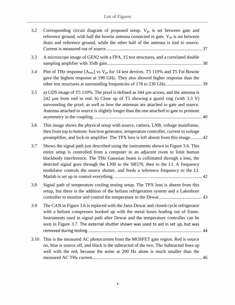
microbolometer. As shown in Figure 1.4 the microbolometer is made of several elements
including an absorbing material, a cavity between the absorbing membrane and mirror above the
substrate, two electrodes, a reflector, and a ROIC substrate.
Figure 1.4: Concept image of a microbolometer, with the different elements of absorbing layer,
reflector, cavity, electrodes, and ROIC substrate. Reprinted from [3].
The absorbing material is a membrane typically made of an amorphous Si or some type of
vanadium oxide (i.e. VOx) and is tens to hundreds of nanometers in thickness. The membrane
only absorbs a fraction of the incident light, so the underside of the membrane and a mirror
located on top of the membrane create a cavity for resonance [3]. The distance of the cavity is
used to optimize the microbolometer to the desired detection frequency and is sometimes filled
with a dielectric material to aid with response. Figure 1.4 from [3] and work conducted in [6] list
the resonant cavity as λ/4 and λ/2 in distance depending on application. Microbolometers are a

1. Introduction
10
desired technology due to the ease of operation, reliability, sensitivity at room temperature, low
cost, and ease of integration with silicon microcircuits; all useful when creating high number
focal plane arrays [56].
Three companies that have taken advantage of these properties of microbolometers to design
commercialized THz high density focal plane arrays are: NEC (Japan), INO (Canada), and CEA-
LETI (France). As shown in Figure 1.5a, the NEP of their microbolometer arrays range from 10
pW to hundreds of pW with NEC offering the lowest. NEC was the first company to take
advantage of changing the sheet resistance of the absorption layer; by doing so it was possible to
optimize the absorption of different THz frequencies. LETI made optimizations to the
technology by adding antennae to their microbolometers to further enhance detection at THz (as
was done for Si-FETs). Figure 1.5b, shows a typical LETI microbolometer structure with the
antennae integrated into the design on top of the dielectric material filled cavity. With the
antennae integrated design, LETI have achieved responsivity values of 5 - 14 MV/W [6]. While
microbolometers are normally designed for operation at 8-14 microns, NEC, INO, and LETI
have achieved detection of frequencies between 1 and 7 THz.

1. Introduction
11
a)
b)
Figure 1.5: a) shows the NEP of the commercialized microbolometer arrays for the three
companies NEC, INO, and CEA-LETI. b) shows the schematics of a LETI microbolometer pixel
with antennae integrated into the design to enhance THz response. a) reprinted from [56], b)
reprinted from [6].
The largest limitations of microbolometers is 1/f noise located in the absorbing material; the
lower the frequency and smaller the bolometer pitch, the higher it will be. One solution of
decreasing 1/f, is to increase the temperature coefficient of resistance (TCR) of the absorbing
material. This has a negative effect of increasing the dynamic range requirements of the ROIC
[65]. NEC overcomes the 1/f of its cameras by using a lock-in technique, which increases the

1. Introduction
12
size of the detection set up (considering Lock-Ins tend to be large instruments) [66]. Work
provided by [65] creates a figure of merit (FOM) dependent on the noise equivalent differential
temperature (NEDT) and the thermal time constant. [65] then discusses different methods of
modifying microbolometers to improve that FOM; each improvement however, comes with a
drawback on NEDT and/or thermal time constant. One method is to reduce pixel pitch which
reduces system size, this increases NEDT which increases the FOM (smaller the better). Another
method is to reduce thermal conductance of the electrodes attached to the membrane, seen in
figures 1.4 and 1.5b, to reduce NEDT; however, this leads to an increase in time constant and
thereby an increase in FOM. If the electrode thermal conductance is increased for reduction in
time constant, there is an increase in NEDT. The benefits and limitations of microbolometers
keep them in competition with photonic detectors such as SBDs and FETs.
Two other types of room temperature bolometer setups that exist are Golay cells and
pyroelectric detectors. Golay cells contain gas filled cavities held by a window for receiving
radiation and a flexible membrane capable of changing shape with temperature (as shown in
Figure 1.6a) [12]. As incident radiation enters the cavity it heats up the gas which deforms the
membrane, bending the light that leaves the cavity. The bending of the light can then be related
back to the incident power hitting the cavity. Pyroelectric detectors act as capacitors that change
capacitance with incident radiation. A thin film is deposited on one of the plates of the capacitor
(the pyroelectric material seen in Figure 1.6b) and, with an increase of temperature from incident
radiation, creates a polarization change and hence a new capacitance [12]. While both detectors
are able to decrease their size while keeping their frequency of operation, they lose sensitivity by
operating at room temperature (as described in Table 1.2). The two detectors also retain the slow
response times seen in most cryogenic bolometers.

1. Introduction
13
a) b)
Figure 1.6: a) Shows the common layout for Golay cells, where light enters into the cavity, out
the membrane through an optical read-out, then onto the detecting mechanism. b) Shows the
common circuit layout of a pyroelectric detector, where light hits one of the electrodes to cause a
change in capacitance. a) and b) reprinted from [12]
1.2.2 Schottky Barrier Diodes
Schottky Barrier Diodes (SBDs) are used in RF applications where its non-linear I-V (current-
voltage) characteristics aid in detection [14]. SBDs have p-n junction setups, where a Schottky
junction is created from an anode (usually metal) and a cathode (usually n-type semiconductor)
[12]. Figure 1.7 shows the SBD setup just described, where metal contacts are attached to n-type
GaAs at a site called a Schottky junction. At this Schottky contact you end up with a Schottky
barrier, a potential barrier that electrons are confined to unless in a high enough energy state to
escape. Electrons cross from one region to the next through a carrier transport method called
thermionic emission that has been found to be more efficient than diffusion through the barrier
[1]. More on thermionic emission will be discussed as a THz detection mechanism in Chapter 2.
SBDs have a relatively simple fabrication process, generally high response speeds, and are the
only diodes that can operate under 0 DC biasing. It is this zero biasing that allows SBDs to be
sensitive to THz waves.

1. Introduction
14
Figure 1.7: A layout of a SBD fabricated in a CMOS process placed on an intrinsic GaAs
substrate. Two anode contacts are placed on a n++ type GaAs semiconductor material. Metal
contacts provide bias voltage to establish a depletion region. Reprinted from [56]
A disadvantage of SBDs are that they have a low conversion gain [15]. Part of the motivation
of this project is to create a focal plane array. While it is easy to fabricate one or a few of the
SBDs, the ease of make and the cost to make them become a problem the more pixels needed.
1.2.4 Field Effect Transistor
Field Effect Transistors (FETs) offer the most promising potential for THz imaging on a focal
plane array level and have only seen research as a solid-state electronic THz detector as far back
as the early 1990s. Through a process known as Complementary Metal Oxide Semiconductor
(CMOS), they offer much easier fabrication and cost effective methods of establishing focal
plane arrays. However, the CMOS process can be noisy and lead to unwanted effects such as 1/f
and Random Telegraph Noise. These types of noise are dependent on the number of
imperfections (traps) that are created in the FET channel during the fabrication process.
Compared to bolometers, CMOS FETS give higher NEP; however, they operate at room
temperature, are relatively cheaper to fabricate, and have much faster response times. Readout
speed for a FET is limited by cutoff speed and can be on the order of GHz. While SBDs have the
similar problems, operation, and ease of fabrication, FETs are expected to eventually have better
NEP and responsivity as the technology becomes more mature [12].

1. Introduction
15
Since detection with the fabricated Metal-Oxide Semiconductor Field Effect Transistor is the
topic of focus for the work in this thesis, discussion of its history, design, operation, and
detection of THz waves will be discussed in Chapter 2.
1.3 THz Applications
1.3.1 Astronomy
The first application where THz imaging was applied was astronomy, where it servers an
important role [1] [9]. The NASA missions Cosmic Background Explorer (COBE) and Diffuse
Infrared Background Experiment (DIRBE) both showed that half the luminosity of the universe
and 98% of the light emitted since the big bang were in the THz band [9]. This means that a vast
amount of information about our universe since its beginning is located in this EM band.
Additionally, as seen in Figure 1.8, a large amount of interstellar dust is at temperatures where
the blackbody emission is in the THz regime.
Figure 1.8: There are many absorption bands that lie within this region and much of the
background light emitted since the big bang at a temperature of 2.7 K. Reprinted from [1]
It is believed that likely 40,000 individual spectral lines are emitted by molecules and ions
found in these dust clouds and that only around a thousand have been studied with many in the
THz band to yet be mapped with decent spectral resolution [9]. The absorption effects of the
earth’s atmosphere, means that study of the THz region is best achieved from space or high

1. Introduction
16
altitudes, where the atmosphere is thin or nonexistent. It is because of these absorption lines and
the atmospheric reason mentioned in section 1.1 that many astronomical telescopes for the
submillimeter and millimeter are found to be in the upper atmosphere or space. Some examples
of such instruments include the submillimeter wave astronomy satellite (SWAS), submillimeter
probe of the evolution of cosmic structure (SPECS), space infrared interferometric telescope
(SPIRIT), and the Atacama Large Millimeter Array (ALMA) [9] [1]. Most, if not all, of these
instruments use deeply cooled bolometers so that high sensitivities can be achieved [16].
1.3.2 Security
Figure1.9: Shows two types of THz setup implementation for security. a) transmission mode
good for seeing through bags and containers, while b) reflection mode is good for detecting
dangerous object on people. Reprinted from [17]
The THz band has the potential to play an important role in security applications, from explosive
and narcotics detection to biometric security [2]. THz has three attributes that make it
particularly applicable to this field [17]. The first is that THz can easily pass through most non-
metallic and non-polar materials like cardboard, clothing, shoes, and bags, with little absorption.
A focal plane array of THz sensitive pixels would be particularly useful in the application shown
in Figure 1.9, where it would provide a large instantaneous field of view. This is very useful, for
example, in airport security systems, for detection of guns, knives, and liquids; where scanning
systems using single element THz detectors cause delay and long lines. Figure 1.10 shows an
example an image taken with a reflective THz system (i.e. as shown in Figure 1.9b). Valuable
information not seen in the visible image (Figure 1.10a) is revealed in the THz region (Figure
1.10b). The second attribute for application of THz imaging in security is the non-ionizing

1. Introduction
17
characteristic that would allow for safe operation for the people being scanned at the airport and
for the operator.
Figure 1.10: a) is an image of a person in the visible range of the EM spectrum. b) is the THz
image of the same man revealing that under his jacket is a gun and another metal object. The
image was taken with TES sensors operating at 0.35 THz, 5 m from the subject showing the
effectiveness of a system like this. Reprinted from [3]
The third THz attribute of value to security would be that many explosives and biological
agents have characteristic THz absorption features that can be used as a fingerprint to identify
them even when concealed. Explosives such as c-4, HMX, TNT and TNS as well as drugs like
methamphetamines have absorption features in their transmission spectra in the THz range that
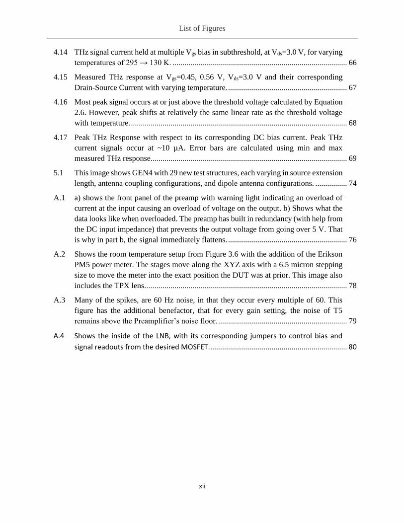
can be distinguished from other materials [17]. Figure 1.11 shows an example of THz absorption
features being used to distinguish three drugs that are nearly identical in the visible domain.
When law enforcement is faced with three identical bags such as in Figure 1.11a, using
techniques in Figures 1.11b and 1.11c, they can display an image such as Figure 1.11d to
distinguish the type of drug without ever opening the bag. Other established means of security
imaging include Millimeter Wave imaging systems (MMWs). MMWs normally operate around
30 GHz and below. THz imaging offers better spatial resolution and a larger range of
spectroscopic signatures [17]. For example, explosives tend to have low vapor pressure
signatures that are unable to be detected by MMWs however, these vapor pressure signatures
1. Introduction
18
have key spectroscopic fingerprints that are detectable in the THz range with suitable detectors
[17].
a) b)
c) d)
Figure 1.11: a) shows a visible image with little information on MDMA, methamphetamine, and
aspirin. When THz absorption features are measured in b) and c) between 1 and 2 THz, each
drug exhibits different absorption behaviors. The THz absorption features are overlaid with the
visible image in a) to display each drug as different from each other in d). a) through d) are
Reprinted from [62]
1.3.3 Medical Applications
There is continuing interest in applying THz imaging and techniques to medical imaging. THz
radiation is non-ionizing and poses less health risk during exposure vs UV and X-rays, making it
a substitute in some cases from UV and X-ray imaging. Other applications in medical imaging

1. Introduction
19
include disease diagnostics, label-free DNA sequencing, and tissue identification [18]. In
detecting diseases, direct imaging of tumors, skin, or wounds through bandaging becomes viable
and in vivo (experimentation on live organisms without removing sample) imaging for vascular
and gastro-intestinal disease diagnosis are being evaluated [18]. As for tissue identification, in-
vivo and in-vitro (experimentation on living organisms by removing samples) detection is being
explored for refractive index changes in the THz on surface skin legions. THz imaging is also
being studied in the evaluation of assessing burn damage.
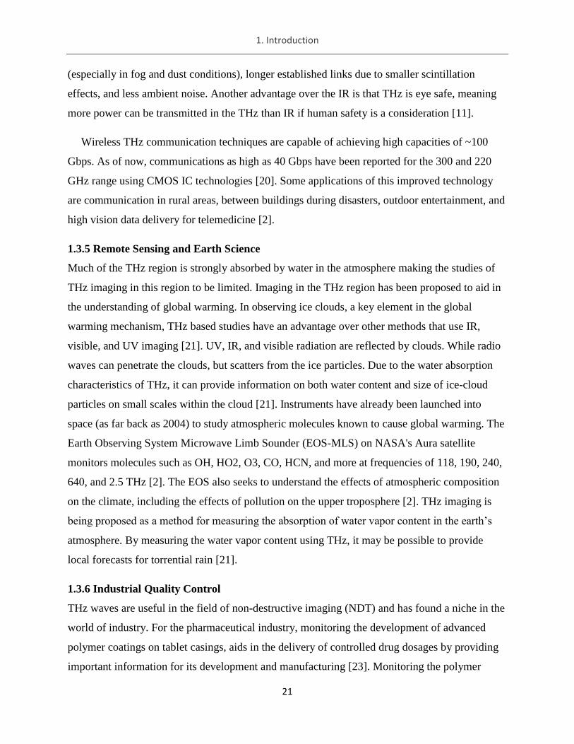
Companies such as TeraView have developed terahertz pulsed imaging (TPI) detectors for
skin and various surface cancers. Using TPI methods, TeraView have also made an intra
operation THz probe, shown in Figure 1.12a, for imaging of cancerous tissue, such as breast
cancer, to aid in the removal during operation. Normally, during breast cancer surgery, surgeons
make a best estimate of where to remove diseased tissue [19]. Then over the course of 2-3
weeks, the tissue is tested for surrounding healthy tissue to show that the entire cancer has been
removed. In 30% of cases, women are called back for a second operation because not all
cancerous material has been removed leading to increase risks and cost [19]. Cancerous, fatty,
and fibrous tissues all have different THz absorption and refractive indexes as shown in Figure
1.12b. By using TPI methods during the operation, the surgeon can distinguish between the three
main tissues and have a higher chance of removing the entire cancer in a single operation.
1. Introduction
20
a)
b)
Figure 1.12: a) Shows TeraView’s TPS Spectra 3000 probe while b) shows the absorption and
refractive indexes of cancerous, fibrous, and fatty tissues. There are clear differences between the
three tissues that can be seen in the THz band. a) and b) Reprinted from [19] and [63]
1.3.4 Communications
While it remains true that THz waves have poor transmission over long distances through the
atmosphere, it has been proposed as a means of short distance communication. Some of the
advantages of THz communication over its lower frequency counterpart MMW are the ultra-high
bandwidth, unregulated frequencies, directional beams, and high security [11]. The directional
beams benefit comes from the fact that THz waves have less free space diffraction than those in
the millimeter range. Advantages over using the infrared (IR) include lower attenuation
1. Introduction
21
(especially in fog and dust conditions), longer established links due to smaller scintillation
effects, and less ambient noise. Another advantage over the IR is that THz is eye safe, meaning
more power can be transmitted in the THz than IR if human safety is a consideration [11].
Wireless THz communication techniques are capable of achieving high capacities of ~100
Gbps. As of now, communications as high as 40 Gbps have been reported for the 300 and 220
GHz range using CMOS IC technologies [20]. Some applications of this improved technology
are communication in rural areas, between buildings during disasters, outdoor entertainment, and
high vision data delivery for telemedicine [2].
1.3.5 Remote Sensing and Earth Science
Much of the THz region is strongly absorbed by water in the atmosphere making the studies of
THz imaging in this region to be limited. Imaging in the THz region has been proposed to aid in
the understanding of global warming. In observing ice clouds, a key element in the global
warming mechanism, THz based studies have an advantage over other methods that use IR,
visible, and UV imaging [21]. UV, IR, and visible radiation are reflected by clouds. While radio
waves can penetrate the clouds, but scatters from the ice particles. Due to the water absorption
characteristics of THz, it can provide information on both water content and size of ice-cloud
particles on small scales within the cloud [21]. Instruments have already been launched into
space (as far back as 2004) to study atmospheric molecules known to cause global warming. The
Earth Observing System Microwave Limb Sounder (EOS-MLS) on NASA's Aura satellite
monitors molecules such as OH, HO2, O3, CO, HCN, and more at frequencies of 118, 190, 240,
640, and 2.5 THz [2]. The EOS also seeks to understand the effects of atmospheric composition
on the climate, including the effects of pollution on the upper troposphere [2]. THz imaging is
being proposed as a method for measuring the absorption of water vapor content in the earth’s
atmosphere. By measuring the water vapor content using THz, it may be possible to provide
local forecasts for torrential rain [21].
1.3.6 Industrial Quality Control
THz waves are useful in the field of non-destructive imaging (NDT) and has found a niche in the
world of industry. For the pharmaceutical industry, monitoring the development of advanced
polymer coatings on tablet casings, aids in the delivery of controlled drug dosages by providing
important information for its development and manufacturing [23]. Monitoring the polymer
1. Introduction
22
casing development is done with NDT methods and the spectral fingerprints of drugs absorbed
the THz band. Other uses are to be found in the food and agricultural industry where THz NDT
methods can be used to find contaminants in food packaging without having to open them [23].
Also, due to the heavy absorption by water in the THz band, damage in fruits and vegetables can
be observed [2].
The semiconductor industry has also found uses for terahertz imaging. Terahertz time domain
spectroscopy has been proved capable of evaluating semiconductor wafer properties such as
mobility conductivity, carrier densities, and visualize doping level of ion-implanted silicon
wafers [2].
1.4 Thesis Details
The purpose of the work in this thesis is to aid in the creation of a high pixel density FPA for
THz detection, fabricated using a commercially available CMOS process [10]. Detectors are first
being developed for the 0.2 THz atmospheric window in the hopes of using the FPA for standoff
detection in security, medical, and industrial applications (like those mentioned in Section 1.3)
[24]. The performance goal for this THz radiation sensitive FPA is to show background limited
performance at room temperature and achieve a spatial resolution of less than 0.5 cm at a 5-10 m
distance [10] [24]. This goal is to be achieved by first testing a variety of pixel design including
varying both antenna and MOSFET design. This thesis will focus on evaluating one of the pixel
designs over a range of temperatures to come to a better understanding of its operation and
proper biasing parameters.
The evaluation of the pixel design is to support research of a collaboration between Harris
Corporation, the University of Rochester (UR), and the Rochester Institute of Technology (RIT).
The collaboration was brought together by Center for Emerging and Innovative Sciences (CEIS);
an advanced technology center, located at the UR, that is funded by the New York State
Department of Economic Development. The goal of CEIS is to match funding with corporate-
sponsored research and partner it with UR and RIT researchers in hopes of increasing impact on
research and development of advanced technology [25]. Characterization of individual test
structures in this thesis is carried out in the Laboratory for Advanced Instrumentation Research
(LAIR) at the Chester F. Carlson Center for Imaging Science, RIT.
1. Introduction
23
1.5 Summary
While the idea of THz imaging and detection is not new, this spectral region has seen a
renaissance of interest recently due to advances in materials and semiconductor processing. The
THz band of the EM spectrum offers unique properties that researches wish to take advantage of
in many applications of security, industry, astronomy, communications, and earth sciences.
Various detector designs for THz detection do exist and each offers its own benefits and
drawbacks. However, due to the commercial availability and relatively low cost of silicon
foundry based manufacturing, a CMOS THz detector is particularly attractive. This thesis will
evaluate one of the best performing MOSFET THz detectors fabricated and optimized to operate
at 0.2 THz, to better understand performance and limitations of the device.

24
2. Theory
2.1 MOSFET Basics
2.1.1 MOSFET Structure and Operation
The idea of the field effect has been researched the 1920's; however, it wasn't until 1930 that the
first Field-Effect Transistor (FET) was proposed by Lilienfeld and Heil [26] [27] [28]. Lilienfeld
and Heil did not understand enough about the device to create a working one, so it wasn't until
1948 that the first successful FET made by Shockley and Pearson of Bell Laboratories. 12 years
of further research by Kahng and Atalla yielded the Metal-Oxide Semiconductor Field-Effect
Transistor (MOSFET) structure. Since then, MOSFETs have revolutionized integrated circuits
(ICs) and have been studied many times over for use in multiple applications [26] [29]. There are
many types of FETs; but the MOSFET belongs to the metal insulator semiconductor (MIS)
family. Since most of the MIS family use Si as a substrate and silicon-oxide SiO2 as the
insulation, the MOS term was given [27]. A MOSFET in its simplest form is an electronic switch
with 4 main terminals: gate, source, drain, and substrate. The n-type MOSFET (of which is used
in this work) is made with a p-type semiconductor substrate on which two n+ regions are put in
through ion implantation. Then through a thermal oxidation process a layer of SiO2 is grown on
the surface of the substrate with a metal planted on top that acts as the gate terminal [27]. The
basic structure of the MOSFET is presented in Figure 2.1:

2. Theory
25
Figure 2.1: VD is drain bias, VG is gate bias, d is insulator thickness, L is the length of the
channel (and often the gate), and Z is the channel width. Source is often held at ground in many
applications, though it is the line of detection for us. VBS is the substrate bias, that for us, is held
at ground. Reprinted from [26]
Conduction of the MOSFET channel is controlled by the voltage applied to the gate terminal.
At a state of zero bias, theoretically the channel is under equilibrium and the carriers (in our case
electrons) are unable to flow from source region to drain region [27]. Even at a state of zero bias
however, there is still come degree of conduction for electrons to travel from source to drain; this
is known as leakage current. Bias to the gate terminal creates a positive potential at the gate-
oxide layer which attracts electrons to the channel surface, creating a depletion region below in
the substrate [26] [27]. When enough gate voltage is applied to establish a good conductive
channel it is known as the threshold voltage (Vth). While conduction is enabled the source region
acts as an emitter of carriers and the drain region collects them. But when a voltage is applied
across drain and source (Vds), that increases the potential difference between the source side
(which is at zero) and the drain side [26]. As the potential on the drain side increases due to
increasing Vds we see a rise in potential at the drain side until the electron velocity becomes
constant and current is unable to increase [4] [26]. This is known as saturation of the channel,
and the region at the drain is known as the pinch off region [27]. If Vds is increased further the
pinch off moves closer to the source region. For applications where leakage current is too high
under threshold biasing conditions, a bias to the substrate terminal is applied. By doing so, Vth is

2. Theory
26
increased and the leakage current is decreased, however, when decreasing leakage current is not
needed, the substrate terminal is often held at ground (as is the case of our MOSFET).
2.1.2 MOSFET I-V Characteristics
To help better understand the plasmonic and thermionic detection methods, as well as better
analyze our test device, it will be important to derive the I-V characteristic concepts of a typical
MOSFET for drain current vs gate-source voltage (Id vs Vgs).
When voltage is applied across gate and source (Vgs) of the MOSFET it attracts electrons to
the surface of the substrate establishing a conductive channel; this is what’s known as inversion
[27]. As Vgs is increased the channel changes into different modes of operation, each containing
different types of inversion. Figure 2.2 shows the change of modes of operation and inversion as
Vgs is increased from 0 V.
Figure 2.2: The different regimes of the modes of operation with increase of Vgs are shown. The
figure also notes a parabolic like behavior that will be seen in chapter 4. Adapted from [27].
The first mode of operation is subthreshold, when Vgs < Vth. It is desired for the drain current
in subthreshold to be as small as possible. MOSFETs are often operated in this regime for
devices that require low power usage, like digital circuits and memory devices [30]. There exist
3 regions of the subthreshold mode, 'OFF-State', weak inversion, and moderate inversion. The
‘OFF State’ is the region of the subthreshold mode that is dominated by leakage current. As Vgs
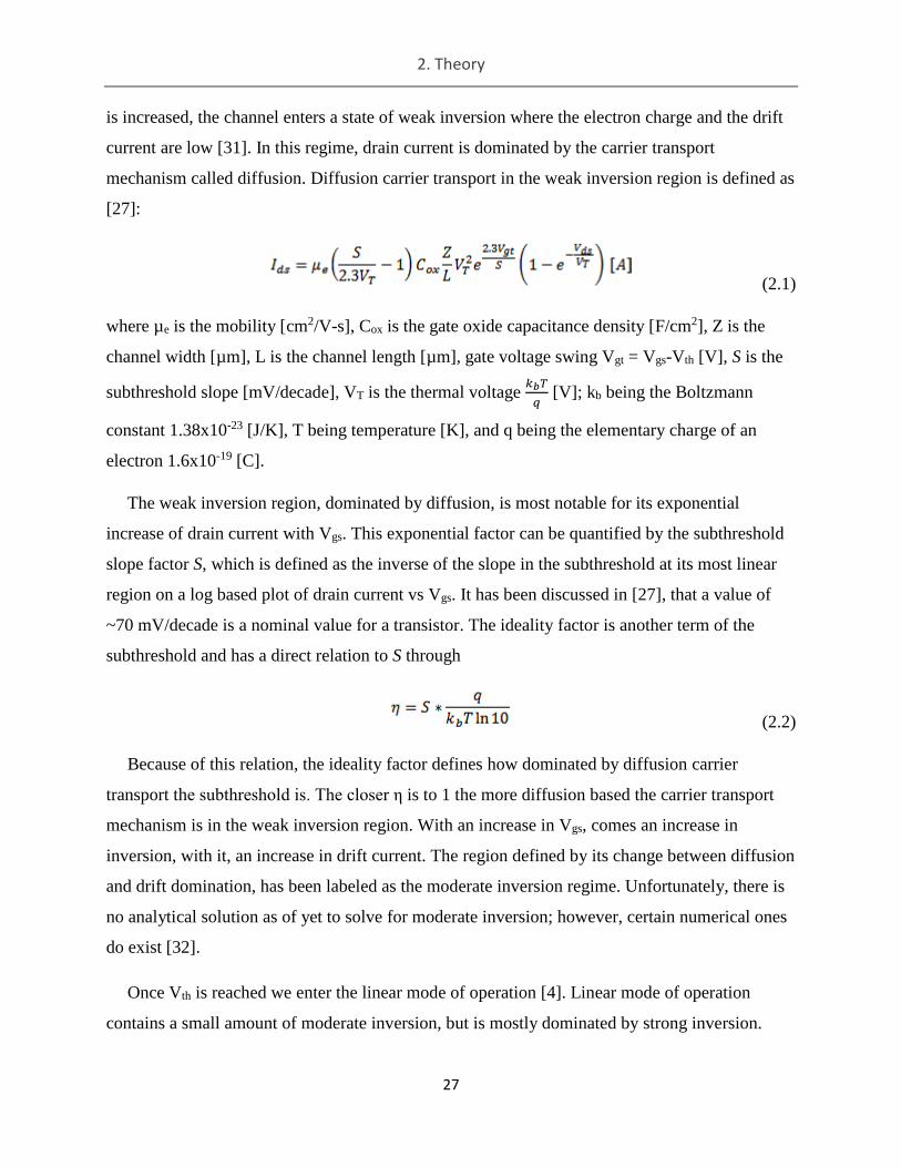
2. Theory
27
is increased, the channel enters a state of weak inversion where the electron charge and the drift
current are low [31]. In this regime, drain current is dominated by the carrier transport
mechanism called diffusion. Diffusion carrier transport in the weak inversion region is defined as
[27]:
(2.1)
where µe is the mobility [cm2/V-s], Cox is the gate oxide capacitance density [F/cm2], Z is the
channel width [µm], L is the channel length [µm], gate voltage swing Vgt = Vgs-Vth [V], S is the
subthreshold slope [mV/decade], VT is the thermal voltage 𝑘𝑏𝑇
𝑞 [V]; kb being the Boltzmann
constant 1.38x10⁻²³ [J/K], T being temperature [K], and q being the elementary charge of an
electron 1.6x10⁻¹⁹ [C].
The weak inversion region, dominated by diffusion, is most notable for its exponential
increase of drain current with Vgs. This exponential factor can be quantified by the subthreshold
slope factor S, which is defined as the inverse of the slope in the subthreshold at its most linear
region on a log based plot of drain current vs Vgs. It has been discussed in [27], that a value of
~70 mV/decade is a nominal value for a transistor. The ideality factor is another term of the
subthreshold and has a direct relation to S through
(2.2)
Because of this relation, the ideality factor defines how dominated by diffusion carrier
transport the subthreshold is. The closer η is to 1 the more diffusion based the carrier transport
mechanism is in the weak inversion region. With an increase in Vgs, comes an increase in
inversion, with it, an increase in drift current. The region defined by its change between diffusion
and drift domination, has been labeled as the moderate inversion regime. Unfortunately, there is
no analytical solution as of yet to solve for moderate inversion; however, certain numerical ones
do exist [32].
Once Vth is reached we enter the linear mode of operation [4]. Linear mode of operation
contains a small amount of moderate inversion, but is mostly dominated by strong inversion.

2. Theory
28
Strong inversion indicates the domination of drift as the minority carrier transport mechanism.
The current flow from drain to source in this mode is treated like the flow through a resistor and
is defined as [4] [26] [27] [33]:
(2.3)
It is important to note that equation 2.3 goes to zero once Vgs=Vth. This would be the case for
an ideal transistor acting as an electronic switch. However, subthreshold evaluation shows that
actual FETs do not behave ideally.
The final mode of operation is saturation. In this region Vds is high enough for the gate
voltage swing to pinch off as stated in Section 2.1.1, and is defined in [33] as:
(2.4)
Saturation is not readily identifiable on an Ids vs Vgs plot, so it is observed on an Ids vs Vds
plot. Figure 2.3 shows a typical Ids vs Vds plot, with different regions identified.
Figure 2.3: Standard model for drain I-V curve of a MOSFET showing standard regions of
operation compared to drain biasing. The linear region is known as the Ohmic/Triode region and
behaves like a resistor. The non-linear region is where current begins to saturate. The saturation
region is where the velocity of the carriers of the channel can no longer become faster, leading to
flat curve as shown. Adapted from [26]
2. Theory
29
2.2 Temperature Effects on MOSFETs
THz detection for Si-MOSFETs with drain-source current (Ids) at varying temperatures will be
characterized in Chapter 4, therefore, this section will discuss the temperature effects on drain
source current of Si-MOSFETs. Temperature is an important variable in the operation of a
semiconductor; it effects mobility, electron density, diffusion, saturation, current density,
threshold voltage, and more [34]. For Ids, the mode of operation determines its dependence on
temperature. In subthreshold mode equation 2.1 contains both proportional and exponential
dependencies on temperature, these temperature dependences are µe, VT, Vth, and S.
For context, mobility is the result of several different scattering mechanisms of electrons in
the inversion layer, each with some type of temperature dependency to them. A general term for
mobility is defined in [33] as:
(2.5)
where µ0 is the mobility at room temperature [cm2/V-s], T0 is room temperature [K], and k is an
empirically derived constant. Mobility has derivations from the intrinsic carrier concentration
which has a dependence of 1.5 on change in temperature, so k for the discussion performed in
Chapter 4 will be 1.5 [27].
For threshold voltage an empirically derived temperature relation found in the works of [31]
[33] [34] is defined as:
(2.6)
where Vth0 is the nominal threshold voltage that is independent of temperature, alpha is an
empirical constant said to be between 3 and 0.5 mV/K, and T0 is the temperature [K] in which
the nominal threshold voltage occurs. S from equation 2.2 also has a T relation in VT, and is
expected to decrease with decrease in temperature. Subthreshold decreases with decreasing
temperature and does so exponentially with the temperature dependencies in the exponential
term being the dominant factor.
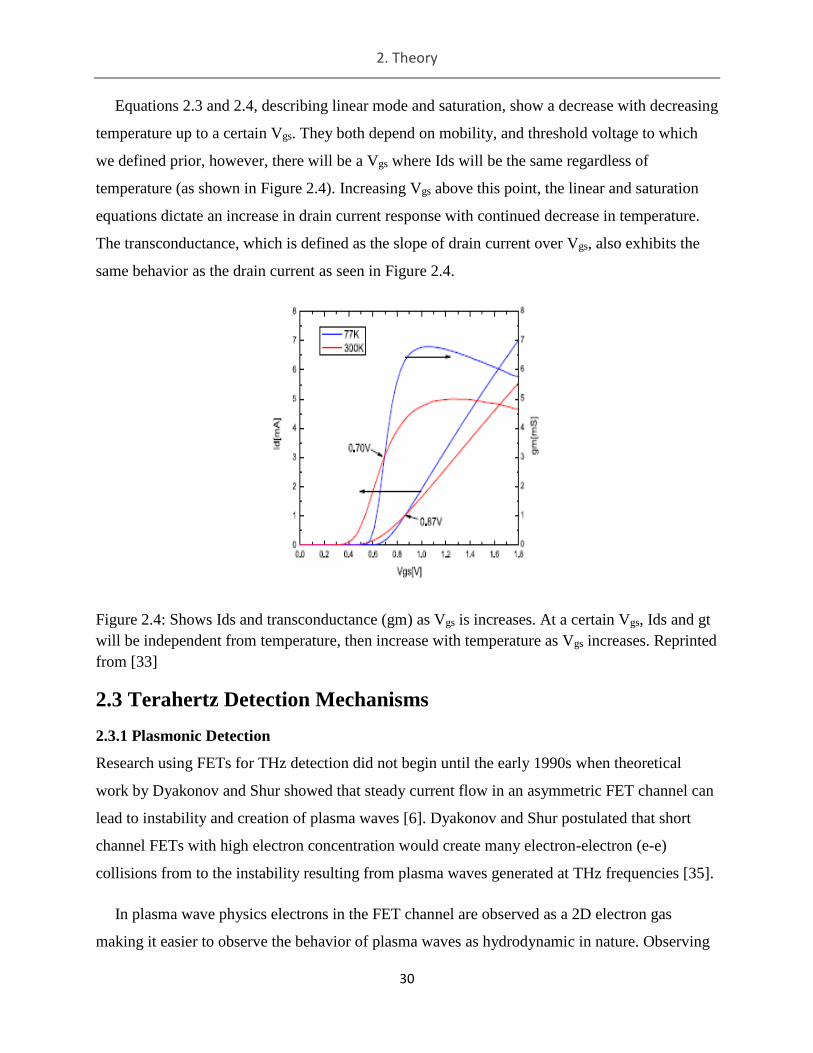
2. Theory
30
Equations 2.3 and 2.4, describing linear mode and saturation, show a decrease with decreasing
temperature up to a certain Vgs. They both depend on mobility, and threshold voltage to which
we defined prior, however, there will be a Vgs where Ids will be the same regardless of
temperature (as shown in Figure 2.4). Increasing Vgs above this point, the linear and saturation
equations dictate an increase in drain current response with continued decrease in temperature.
The transconductance, which is defined as the slope of drain current over Vgs, also exhibits the
same behavior as the drain current as seen in Figure 2.4.
Figure 2.4: Shows Ids and transconductance (gm) as Vgs is increases. At a certain Vgs, Ids and gt
will be independent from temperature, then increase with temperature as Vgs increases. Reprinted
from [33]
2.3 Terahertz Detection Mechanisms
2.3.1 Plasmonic Detection
Research using FETs for THz detection did not begin until the early 1990s when theoretical
work by Dyakonov and Shur showed that steady current flow in an asymmetric FET channel can
lead to instability and creation of plasma waves [6]. Dyakonov and Shur postulated that short
channel FETs with high electron concentration would create many electron-electron (e-e)
collisions from to the instability resulting from plasma waves generated at THz frequencies [35].
In plasma wave physics electrons in the FET channel are observed as a 2D electron gas
making it easier to observe the behavior of plasma waves as hydrodynamic in nature. Observing
2. Theory
31
plasma waves as hydrodynamic is possible because the e-e collisions do not degrade the electron
gas due to the Pauli principle, allowing for there to be lack of external friction [35]. By allowing
the 2D electron gas to be viewed as a fluid, Dyakonov and Shur in [36] defined the electron flow
with Euler’s formula:
𝛿𝑣
𝛿𝑡+ 𝑣
𝛿𝑣
𝛿𝑥+
𝑞
𝑚
𝛿𝑈
𝛿𝑥+
𝑣
𝜏= 0 (2.7)
where U is the longitudinal electric field in the channel [V], v is the local electron velocity [m/s],
m is the mass of an electron 9.11x10⁻³¹ [kg], x is the position in the FET channel [m], and τ is the
momentum relaxation time [s]. In solving this equation, Dyakonov and Shur used gradual
channel approximation as boundary conditions in [36] to obtain the fluid relation:
(2.8)
To evaluate the Plasmon fluid relation further it will be necessary to mention the following
parameters: Average free time between electron collisions:
𝜏𝑟 =𝜇𝑒𝑚𝑒
∗
𝑞 [𝑠] (2.9)
where me* is the effective electron mass in silicon (.19*9.11e-31 kg). The plasmon wave
velocity:
𝑠𝑜 = √𝜂𝑘𝑏𝑇
𝑚𝑒∗ [
𝑚
𝑠] (2.10)
(2.11)
(2.12)
where sp is the plasmon velocity, Vgt is the gate voltage swing. And finally the fundamental
plasma frequency determined by:
(2.13)

2. Theory
32
Gate length and plasma velocity will determine the frequency at which the FET will produce
the highest detection, as shown in equations 2.12 and 2.13. Depending on how these parameters
are set up, it is possible to have two types of plasmonic detection: resonant and non-resonant.
Resonant detection (where ω0τr >1) is only occurs when the gate length is short enough and the
electron mobility is high enough. Since Si-MOSFETs have low electron mobility, resonant
detection does not occur in the channel under most circumstances, therefore, resonant detection
will not be covered.
2.3.2 Non-Resonant Detection
Figure 2.6: Shows Broadband Plasmonic THz Detection. As the THz wave hits the MOSFET on
the right, the electrons are excited in an oscillation that becomes overdamped as the electrons
reach the drain region. Adapted from [4].
For Si-MOSFETS and other FETs of short gate length and low mobility where resonance quality
factor ω0τr << 1, non-resonant detection (or broadband detection [36]) is the predominant
detection mechanism. In broadband detection, the plasma wave is over-dampened before
reaching the drain as shown in Figure 2.6. Many studies, such as [4] [6] [37] [38] [39], have
evaluated the plasmon fluid equation 2.8 for photo induced DC voltage broadband detection as:
(2.15)

2. Theory
33
Where Ua is the photo induced AC voltage onto the gate leads to the DC rectification of voltage
at the drain ΔUdc, that is measured out. Q and the gate leakage factor κ are defined as:
𝑄 =𝐿
𝑠𝑝 √
𝜔0
2𝜏𝑟 (2.16)
𝜅 =𝑗0𝐿2𝑚𝑒
∗𝑞
2𝐶𝑜𝑥𝜏𝑟𝜂2𝑘𝑏𝑇2 (2.17)
Where j0 is the gate leakage current density. For JFETs j0 is known to be ~1 pA, however, as bias
to the drain is increased, so is j0 [29].
Equation 2.15 only gives the rectified DC voltage at the drain region with an open drain
configuration (i.e. where signal is measured between drain and source and neither is held at
ground). It has been shown by other works, such as [4] [40] [39] [41], that by adding an induced
drain current to the MOSFET you can increase the photo detection by a sharp amount.
The increased response is seen as:
(2.18)
Where lambda is the ratio of drain current density to the saturation current density. As lambda
approaches 1 the detector response increases dramatically. According to work done in [38], with
an Ids=0, the previous equation should yield the open drain response, so equation 2.18 can be
rewritten as:
(2.19)
Where is the open drain response without drain current enhancement is ΔUdc0 [V].
2.3.4 Thermionic Emission Detection
Thermionic Emission (TE) is a carrier transport mechanism associated with the potential barrier
height, and is found in devices with semiconductor-metal contacts like schottkey diodes. In order
for TE to work, the barrier region must not be dominated by diffusion; on the other side of the
potential barrier the material must be metal or an n-type semiconductor so that a potential

2. Theory
34
difference can be created [26]. When the majority carriers contain enough energy or when the
barrier is lowered, they are injected over the barrier, which is then measured as current flow [26].
Figure 2.7 shows TE in comparison with the diffusion carrier transport mechanism, where
electrons have enough energy to escape over the barrier qϕBn.
Figure 2.7: Barrier region separating the n-semiconductor channel and the N+ doped source
region. Electron more over the barrier qφBn via TE or through it via diffusion. Ec is the
conduction band, EF is the fermi energy level, qφn is the barrier between the conduction band and
fermi level. Adapted from [26]
THz detection from TE has been proposed as an alternative detection method in Si-MOSFETs
over plasmonic detection. The benefits to TE detection is the stronger dependence on applied
THz radiation and MOSFET geometry; by extending the source region it is possible to increase
sensitivity [42].
Depletion of the channel of any free carriers caused while in subthreshold mode, creates a
potential barrier between the source and channel [42]. The large difference in doping
concentrations between the source and channel regions, diffusion would not be dominant over
this potential barrier. When THz radiation is absorbed by the antenna, it creates oscillations in
electron charge at the gate terminal. The relaxation frequency of the silicon (up to 20 THz due to
high mobility), can help the electron density at the source boundary quickly track the oscillations
at the gate [42]. The oscillations create an electric field that linearly builds a potential in the
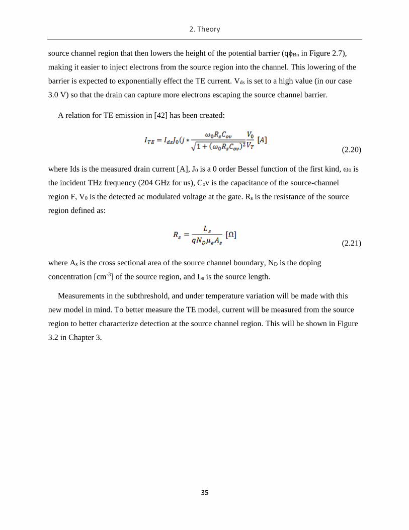
2. Theory
35
source channel region that then lowers the height of the potential barrier (qϕBn in Figure 2.7),
making it easier to inject electrons from the source region into the channel. This lowering of the
barrier is expected to exponentially effect the TE current. Vds is set to a high value (in our case
3.0 V) so that the drain can capture more electrons escaping the source channel barrier.
A relation for TE emission in [42] has been created:
(2.20)
where Ids is the measured drain current [A], J0 is a 0 order Bessel function of the first kind, ω0 is
the incident THz frequency (204 GHz for us), Cov is the capacitance of the source-channel
region F, V0 is the detected ac modulated voltage at the gate. Rs is the resistance of the source
region defined as:
(2.21)
where As is the cross sectional area of the source channel boundary, ND is the doping
concentration [cm-3] of the source region, and Ls is the source length.
Measurements in the subthreshold, and under temperature variation will be made with this
new model in mind. To better measure the TE model, current will be measured from the source
region to better characterize detection at the source channel region. This will be shown in Figure
3.2 in Chapter 3.

36
3. Design and Operation of Low Noise Test Setup:
3.1 Design and Fabrication of GEN2 Test Device
3.1.1 Antenna-MOSFET Integration
On its own the Si-MOSFET is a poor detector of THz radiation, thus many works such as [4]
[24] [43], use antennae to collect the THz radiation like mini telescopes that then couple the THz
to the MOSFET to enhance the detection. By coupling the antennae and MOSFET efficiently,
peak responsivity can be measured. To do this, the antenna's resonant frequency needs to match
the resonant frequency of the MOSFET channel (which can be calculated from Equation 2.13)
[44]. A numerical simulation based on the Finite Difference Time Domain (FDTD) method was
conducted in [45] to determine the best antenna design to use in the range of ~200 GHz. It was
observed that a bowtie shaped antenna had the best broadband response and easiest path to
integration into the CMOS process [24]. Other research groups have noted that when connecting
the antennae to the gate and source terminals rather than the source and drain terminals, they
yielded better THz responses [43]. It is believed that the nonlinearity of antenna coupling is what
yields a better response. When simulations were done with a symmetric setup in [12] it was
found that photocurrents generated in the source side canceled out with the ones generated on the
drain side.
With these ideas of gate-source broadband antennas, and the new various ways that the
MOSFET design will be biased and measured for photocurrent; the resulting device and
corresponding circuit is shown in Figures 3.1 and 3.2.
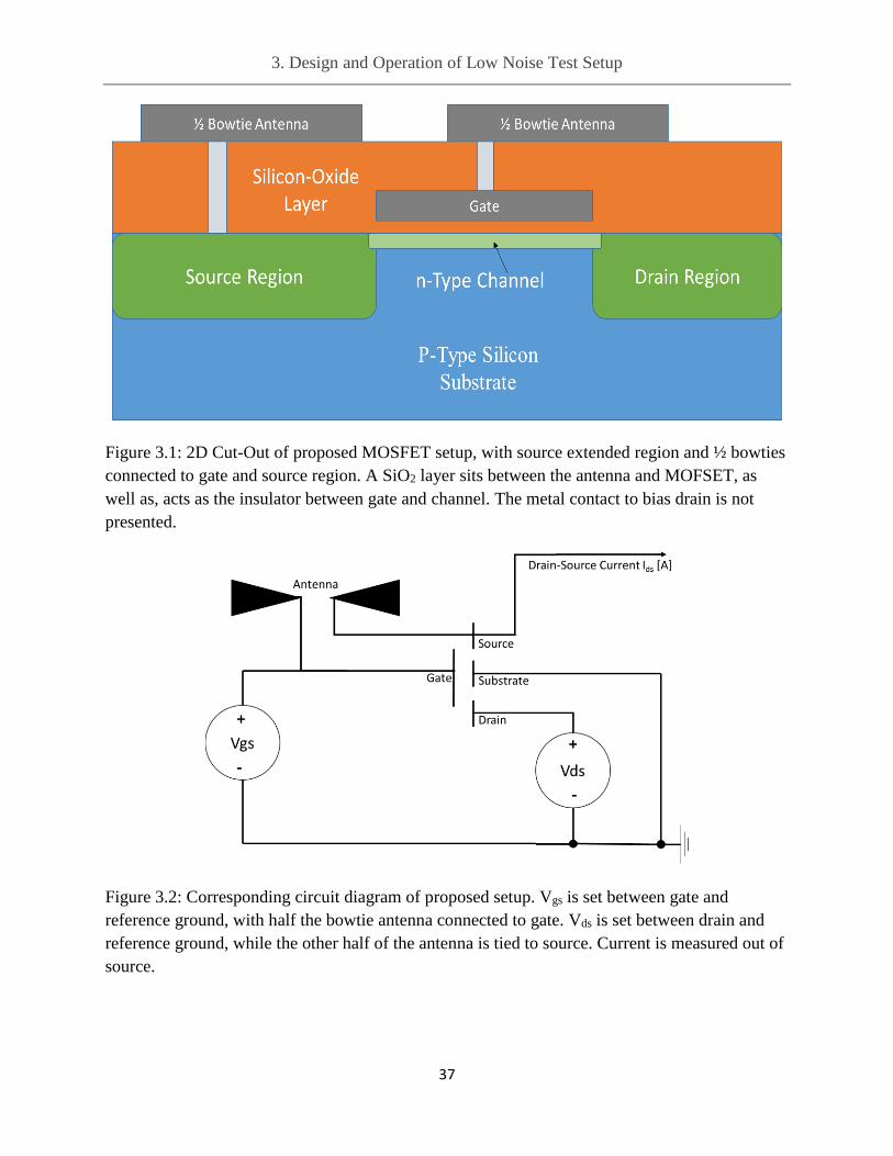
3. Design and Operation of Low Noise Test Setup
37
Figure 3.1: 2D Cut-Out of proposed MOSFET setup, with source extended region and ½ bowties
connected to gate and source region. A SiO2 layer sits between the antenna and MOFSET, as
well as, acts as the insulator between gate and channel. The metal contact to bias drain is not
presented.
Figure 3.2: Corresponding circuit diagram of proposed setup. Vgs is set between gate and
reference ground, with half the bowtie antenna connected to gate. Vds is set between drain and
reference ground, while the other half of the antenna is tied to source. Current is measured out of
source.

3. Design and Operation of Low Noise Test Setup
38
3.1.2 GEN2 Chip and Pixel Design
The chip GEN2, shown in Figure 3.3, was fabricated in a 0.35 micron CMOS process using the
foundry Taiwan Semiconductor Manufacturing Company Limited (TSMC) and the fabrication
house MOSIS. GEN2 was built with substrate thicknesses of 250 nm and is the direct successor
to a first generation chip (named GEN1) which varied source extension and antenna design.
Research in [4] using GEN1 revealed that a MOSFET design with a bowtie antenna tied to gate
and source, and a source extension of 2 µm yielded the highest THz signal response. In response
to this observation, GEN2 was designed to vary antenna structures and various channel width
and length designs of the successful, bowtie, 2 µm source extended GEN1 pixel, here after
referred to as T5.
Figure 3.3: A microscope image of GEN2 with a FPA, 15 test structures, and a correlated double
sampling amplifier with 35db gain.
The FPA in the middle of Figure 3.3 was an experiment to provide a proof of concept array
design for the UR collaborators to verify, therefore it will not be covered in the work of this
thesis. Upon evaluation of GEN2 test structures, T5 110% test device was measured to be the
highest response at around a frequency of 200 GHz.

3. Design and Operation of Low Noise Test Setup
39
Figure 3.4: Plot of THz response [Arms] vs Vgs for 14 test devices. T5 110% and T5 Fat Bowtie
gave the highest response at 198 GHz. They also showed higher response than the other test
structures at surrounding frequencies of 178 to 230 GHz.
T5 110% was an antenna 10% larger than the original GEN1 T5 bowtie, while T5 Fat was a
device with a bowtie antenna design at a broader angle then GEN1 T5 (60° for Fat vs 30° for the
other antennae). Since Figure 3.4 shows T5 110% giving the highest response at ~200 GHz and
showed a similar response to T5 Fat Bowtie, the measurements and analysis in this thesis will
pursue the characteristics of T5 110%. It is expected for T5 Fat Bowtie to differ from T5 110
only in measurement of changing THz frequency, where the THz response is expected to have a
broader spectral range. The spectral range (bandwidth) of T5 110% was measured to be 10 GHz
with a center at 200 GHz. T5 110% also showed polarization of ~94% at a 90° rotation. Figure
3.5 shows the GDS design image of T5 110%. The GDS image shows the source region
extended by 2 µm, with the gate contact above, and the drain contact above the gate.
Surrounding the MOSFET, in purple, is a guard ring powered by a 3.3 V supply. From Figure
3.5a the pixel is measured as 343.95 µm in pitch, while the antenna is 242 µm across with a 30°
angle as stated earlier.

3. Design and Operation of Low Noise Test Setup
40
a) b)
Figure 3.5: a) GDS image of T5 110%. The pixel is defined as 344 µm across, and the antenna is
242 µm from end to end. b) Close up of T5 showing a guard ring (with 3.3 V) surrounding the
pixel; as well as how the antennas are attached to gate and source. Antenna attached to source is
slightly longer than the one attached to gate to promote asymmetry in the coupling.
3.2 Experimental Setup
To measure the response of GEN2 test devices for both THz signal response and DC bias
current, a low noise computer controlled setup.
THz radiation is provided by a VDI tunable Gunn Diode capable of frequencies between 170
GHz and 250 GHz; the source is also equipped with an electronic shutter. The THz radiation
then needs to be collimated by a TPX lens due to it being emitted as a Gaussian beam from the
horn in front of the source. By collimating the Gaussian beam, an even distribution of power
from the source can be applied across GEN2. The Device Under Test (DUT) is enclosed in an
aluminum dewar (nicknamed The CAN) designed by Craig McMurtry from the UR team, while
mounted to a Velmex XYZ motorized stage. All current and voltages being applied to and from
The CAN are routed through a low noise faraday box (named the LNB)1. The LNB contains a
fan out board with jumpers to switch between the 15 different test devices on GEN2. Battery
1 More on the LNB and its construction is described in the appendix section A.4.
2 µm Source
Extension

3. Design and Operation of Low Noise Test Setup
41
operated voltage sources in a SIM900 mainframe, provide the necessary voltages into the LNB
to be routed to The CAN. By operating off of a battery, the addition of 60 Hz noise can be
minimized in the supply voltage lines. From the LNB, the DUT signal current is fed into a
SR570 low noise current to voltage preamplifier, with gains available up to 1 pA/V2. The preamp
output voltage is then fed into a SR850 Lock-In Amplifier (provided by Harris Corporation). The
Lock-In uses a reference frequency from a frequency generator3, so that unwanted signals (aka
noise) from all other frequencies, except the one the signal is modulating at, will be filtered out.
The Lock-In creates a narrow bandwidth that only one’s desired signal frequency can be
detected. More on how this setup uses the LI in data acquisition will be described in section 3.3
and appendix A.3. The frequency generator (FG) in this setup modulates a TTL ON/OFF voltage
from a shutter controller to turn the Gunn Diode's electronic shutter on and off at the specific
frequency the Lock-In’s narrow bandwidth is at (for us that is 200 Hz4). All instruments (except
the FG) in this setup are controlled using MATLAB 2014b from a computer in an adjacent room,
so that there is no human interference. From Chapter 1 it was noted that any blackbody over 10
K, could emit low levels of THz radiation, including humans. Figures 3.6 and 3.7 show the
instrumentation and physical signal path just described.
2 The gain settings could not be set that low. They also needed to be changed with different biasing conditions. More on the use of the preamplifier with data acquisition is described in appendix section A.1. 3 A frequency generator was used instead of an internal LI reference because use this type of setup was the only one that physically allowed the source to be modulated and kept off for shutter close measurements. 4 The reason for use of this specific reference frequency has to do with the SR570 preamp BW and is also described in appendix A.1.

3. Design and Operation of Low Noise Test Setup
42
Figure 3.6: This image shows the physical setup with source, camera, LNB, voltage mainframe,
then from top to bottom: function generator, temperature controller, current to voltage
preamplifier, and lock-in amplifier. The TPX lens is left absent from this image5.
Figure 3.7: Shows the signal path just described using the instruments shown in Figure 3.6. This
entire setup is controlled from a computer in an adjacent room to limit human blackbody
interference. The THz Gaussian beam is collimated through a lens, the detected signal goes
through the LNB to the SR570, then to the LI. A frequency modulator controls the source
shutter, and feeds a reference frequency to the LI. Matlab is set up to control everything.
5 Figure A.2 in the appendix, contains an image with the TPX lens in use.
Camera head
THz
Source
LNB
Voltage
Mainframe
Function Generator
Temperature Controller
Preamplifier
Lock-In

3. Design and Operation of Low Noise Test Setup
43
3.2.1 Cold Temperature Setup
To measure the response of GEN2 test devices for both THz signal response and DC bias current
under changing temperature conditions, the same low noise computer controlled setup as section
3.2.1 was used, but with two added instruments.
Similar to Figure 3.6, the experimental setup is operated with the LI, Preamp, LNB, FG, and
voltage mainframe. However, the TPX lens is absent from this setup. The TPX lens was not
added until much later in the project when cooling was no longer viable. The second difference
in the system was the addition of the Closed Cycle Refrigerator System from Janis Research
Company, Inc. This is a cryogenic system that was used to cool the DUT down to temperatures
of 130 K. To monitor and control the temperature of the refrigeration system, the Lake Shore
Model 321 Autotuning Temperature Controller was used, which was also interfaced with
MATLAB 2014b GUI. Figures 3.8 and 3.9 show the change in experimental testing setup.
Figure 3.8: Signal path of temperature cooling testing setup. The TPX lens is absent from this
setup, but there is the addition of the helium refrigeration system and a Lakeshore controller to
monitor and control the temperature in the Dewar.

3. Design and Operation of Low Noise Test Setup
44
Figure 3.9: The CAN in Figure 3.6 is replaced with the Janis Dewar and closed cycle refrigerator
with a helium compressor hooked up with the metal hoses leading out of frame. Instruments used
in signal path after Dewar and the temperature controller can be seen in Figure 3.7. The external
shutter shown was used to aid in set up, but was removed during testing.
3.3 Data Acquisition
Data acquired using the setups in Section 3.2 explores a simple and automated data acquisition
format to measure THz response and drain current from the DUT.
Data Acquisition list:
1. Connection to all instrumentation by MATLAB Guide User Interface (GUI).
2. Biasing of test enabling, drain, and gate voltages are turned on.
3. Source is turned ON at a modulating frequency of 200 Hz.
4. LI autophase finds largest magnitude of AC signal.
5. Take DUT measurement with (AC) THz signal by sweeping test biasing voltage (either
Vds or Vgs)
6. Source is turned OFF.
7. Take DUT measurement without (AC) THz signal by sweeping test biasing voltage
(either Vds or Vgs)
8. Subtract shutter closed (illumination off) from shutter open (illumination on)
measurement to obtain THz Signal measured

3. Design and Operation of Low Noise Test Setup
45
9. Simultaneously take (DC) Drain-Source Current measurements with aux A/D input in
back of SR850 LI during steps 5 and 7.
For step 2, turning on the biasing voltages test enable, drain and gate is described. Drain and
gate refer to the MOSFET drain and gate terminals as explained in Chapter 2. Test Enable is the
gate terminal to an additional MOSFET located on GEN2 that acts as a switch to allow the use of
the other gate terminals of all test devices. The enable FET must always be switched on first to
allow the operation of any DUT on GEN2.
LI amplifiers operate on technique known as phase-sensitive detection. The LI starts by
generating an internal reference signal at the same frequency as the external frequency (in our
case the function generator at 200 Hz). According to [46] the LI then amplifies the incoming
signal (the MOSFET current) and multiplies it by the internal reference using a phase-sensitive
detector (PSD). The product of the PSD contains two AC signals; one at the difference of the two
frequencies and one at the sum [46]. Since the internal reference frequency and the modulated
frequency are the same, that leaves the detected signal to be:
(3.1)
Where VPSD is the voltage measured by the PSD, VSignal and θSignal are the amplitude and phase
of the signal being measured respectively, and VLI and θLI are the amplitude and phase of the LI
reference function respectively. In step 4, the LI changes its phase to match the incoming signal
to get a phase difference of 0°, yielding a PSD detection signal directly dependent off of the
incoming signal amplitude.
Steps 5 through 9 acquire the DC drain-source bias current and THz response of the DUT
while performing its corresponding test bias sweeps. As the Lock-In collects data, it does so
while the Vgs (or Vds depending on the experiment) is increasing to observe the change in signal
with changing bias voltage. Figure 3.10 shows a typical figure that would be achieved at the end
of step 8. In Figure 3.10 each Vgs has 1024 samples, 512 points are taken with source on and 512
are then taken with source off each with a sampling time of 1 second (512 Hz sampling rate for
each). While the LI creates a narrow bandwidth to only allow signals of ~200 Hz, that includes
not just the modulating 200 Hz signal but also the noise present in the system at 200 Hz. This is

3. Design and Operation of Low Noise Test Setup
46
why there is still a signal present with the source off. To obtain the actual signal and not the
signal + noise, step 8 performs a subtraction, where the 512 source ON points are subtracted
from the 512 source off points to arrive at only the measured signal of the system. Figure 3.10
measured the AC current at the gate created by incident THz waves onto the gate.
Figure 3.10: This is the measured AC photocurrent from the MOSFET gate region. Red is source
on, blue is source off, and black is the subtracted of the two. The Subtracted lines up well with
the red, because the noise at 200 Hz alone is much smaller than the measured AC THz current.
The Lock-In only measures signals being modulated at 200 Hz, so the induced DC bias
current (which is not modulating) from the DUT cannot be measured. So we must use an A/D
converter not under LI conditions. This specific LI model (the SR850) has an A/D converter in
the back of the instrument which simply measures any incoming signal. With it the induced DC
bias current was measured yielding the data shown in figure 3.11.
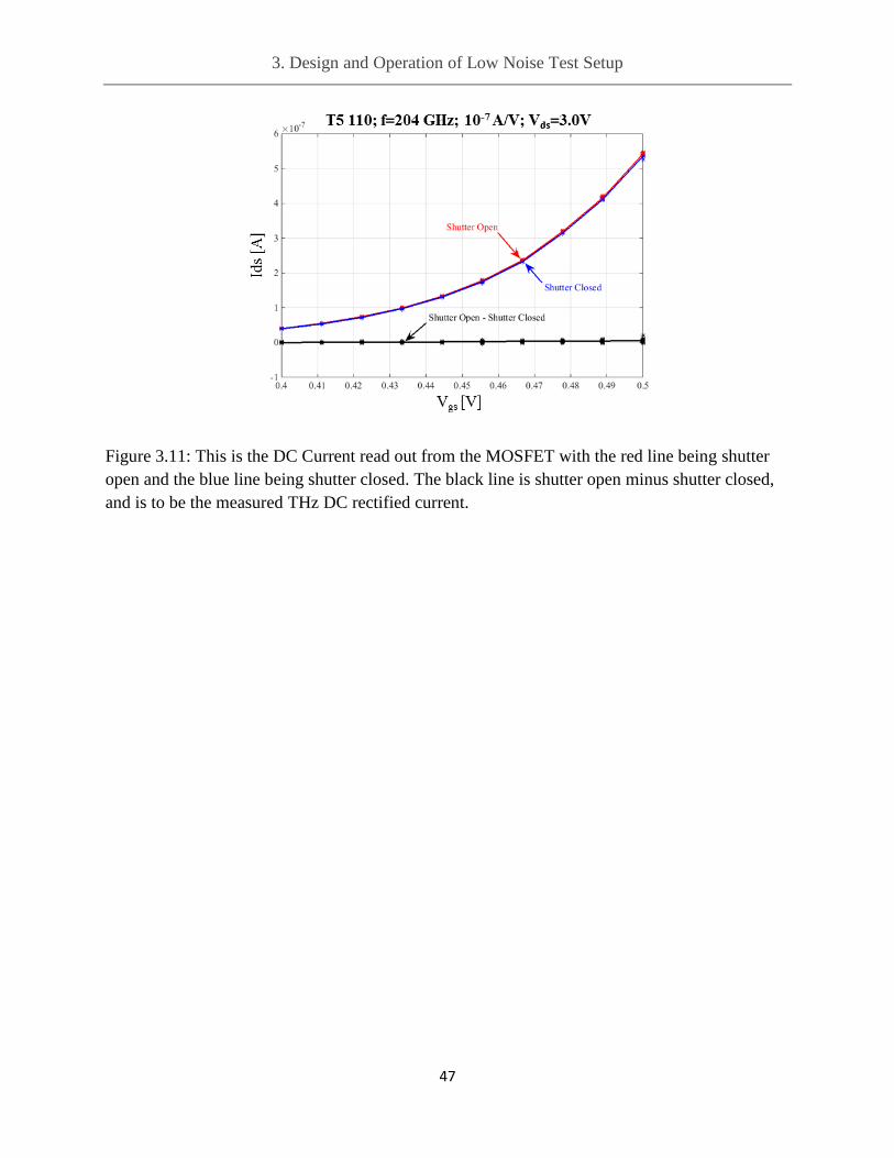
3. Design and Operation of Low Noise Test Setup
47
Figure 3.11: This is the DC Current read out from the MOSFET with the red line being shutter
open and the blue line being shutter closed. The black line is shutter open minus shutter closed,
and is to be the measured THz DC rectified current.

48
4. Results and Discussion
4.1 Characterization of T5 110%
This section seeks to characterize T5 110's DC bias current, at room temperature, with respect to
Vgs, to determine if the MOSFET behavior matches typical curves like those in Chapter 2.
Chapter 2 displayed two methods to characterize the DC bias current, drain-source current (Ids)
vs Vgs plots and Ids vs Vds plots. The analysis and results used in this chapter rely on Ids Vs Vgs
curves to display and monitor the conductance of the FET channel. An aspect that plasmonic
detection response depends on. It is also desired to leave the drain region biased at a high voltage
to observe any thermionic emission detection effects that might occur during THz response
measurement. Figure 4.1 shows T5 characterization by setting Vds = 3.0 V and sweeping Vgs
from 0 to 0.8 V to measure its corresponding Ids. To determine if Figure 4.1 represents a
functioning FET we will use it to characterize threshold voltage, subthreshold minority carrier
transport, and shot noise.
Figure 4.1: T5 110 Drain-Source Current (Ids) taken by sweeping Vgs from 0 to 0.8 V, at Vds=3.0
V. Error bars are calculated from max and min currents measured.
4.1.1 Threshold Vgs Evaluation
Characterization equations for the MOSFET and THz detection mechanisms that were laid out in
Chapter 2 depend on the gate threshold voltage (Vth); so this section seeks to solve for Vth. To

4. Results and Discussion
49
solve for the threshold gate voltage, the Extrapolation in the Linear Region (ELR) method as
described in [47] is used. The ELR method extracts the MOSFET threshold voltage by fitting a
line to the linear region of an I-V curve to find the x-axis intercept. That intercept is then the
threshold voltage. It is important to fit the line to the most linear portion of the I-V curve, since I-
V characteristics can vary after threshold due to mobility degradation [47].
Figure 4.2: An I-V curve with a linear line fit showing that its x-intercept is 0.64 V. This
intercept is threshold voltage. Error bars are calculated from max and min currents measured.
In Figure 4.2 a linear line is fit to Vgs values 0.76 through 0.8 V as this is T5's most linear
region at room temperature. The intercept in Figure 4.2 shows T5 threshold voltage to be 0.64 V.
Any gate-source voltage above 0.64 V is known as the superthreshold mode containing moderate
to saturation inversion, while anything below is known as the subthreshold mode [31] [48].
4.1.2 Subthreshold Characterization
From section 2.1.2, it is expected that weak inversion in subthreshold mode is dominated by
diffusion carrier transport up to moderate inversion when the drift carrier transport mechanism
begins to take over. In Figure 4.3 the subthreshold equation 2.1 was fit to the T5 drain current
data shown in Figure 4.1 where subthreshold was most linear.
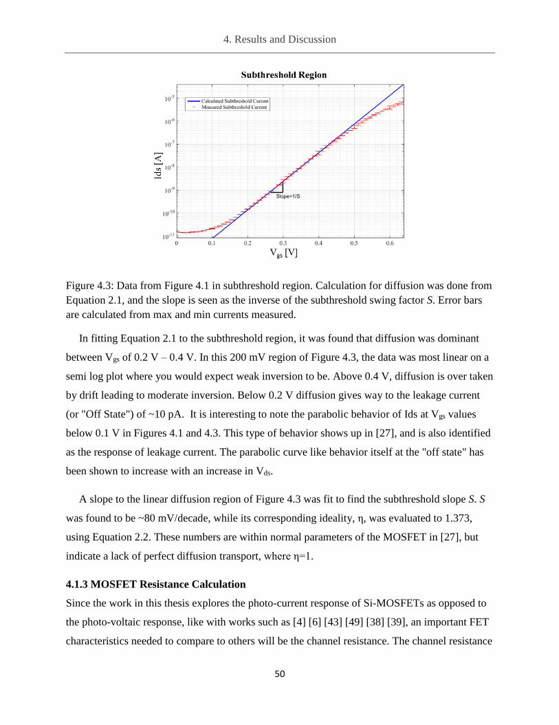
4. Results and Discussion
50
Figure 4.3: Data from Figure 4.1 in subthreshold region. Calculation for diffusion was done from
Equation 2.1, and the slope is seen as the inverse of the subthreshold swing factor S. Error bars
are calculated from max and min currents measured.
In fitting Equation 2.1 to the subthreshold region, it was found that diffusion was dominant
between Vgs of 0.2 V – 0.4 V. In this 200 mV region of Figure 4.3, the data was most linear on a
semi log plot where you would expect weak inversion to be. Above 0.4 V, diffusion is over taken
by drift leading to moderate inversion. Below 0.2 V diffusion gives way to the leakage current
(or "Off State") of ~10 pA. It is interesting to note the parabolic behavior of Ids at Vgs values
below 0.1 V in Figures 4.1 and 4.3. This type of behavior shows up in [27], and is also identified
as the response of leakage current. The parabolic curve like behavior itself at the "off state" has
been shown to increase with an increase in Vds.
A slope to the linear diffusion region of Figure 4.3 was fit to find the subthreshold slope S. S
was found to be ~80 mV/decade, while its corresponding ideality, η, was evaluated to 1.373,
using Equation 2.2. These numbers are within normal parameters of the MOSFET in [27], but
indicate a lack of perfect diffusion transport, where η=1.
4.1.3 MOSFET Resistance Calculation
Since the work in this thesis explores the photo-current response of Si-MOSFETs as opposed to
the photo-voltaic response, like with works such as [4] [6] [43] [49] [38] [39], an important FET
characteristics needed to compare to others will be the channel resistance. The channel resistance

4. Results and Discussion
51
is known to follow Ohms law, where the inverse of the I-V curve slope 𝛿𝑉𝑑𝑠
𝛿𝐼𝑑𝑠 is the resistance; at a
specific Vgs.
Figure 4.4: Resistance of T5 110 channel with respect to Vgs. The resistance decreases with
increasing Vgs.
As Vgs increases the FET will move closer to the "ON" position where conductance of a
current through the channel is more easily allowed, this means a decrease in the resistance of the
electrons path. By time the FET reaches its "ON" position of threshold voltage 640 mV, the
resistance is approximately 1MΩ.
4.1.4 Noise Results for T5 110%
Section 3.2 discusses the steps taken to limit the external noise introduced into the system in the
setup. This means noises inherent to the MOSFET T5 (i.e. 1/f, shot, and thermal noise) should be
left. Using an Agilent Spectrum analyzer (provided by Harris Corporation), the power spectral
density of T5 was measured within a bandwidth of 2 kHz, Vds = 3.0 V, and at room temperature
300 K.

4. Results and Discussion
52
Figure 4.5: Noise power spectral density of T5 110 as Vgs increases, taken within a bandwidth of
2 kHz and at Vds= 3.0 V. It is observed that for most Vgs values, noise is exponentially dependent
on frequency6.
The linear behavior on a semi log of the power spectrum in Figure 4.5 means that, at the
modulating frequency of 200 Hz, T5 is 1/f noise dominated. The choice of this modulated
frequency despite the clear 1/f noise, was due to the SR570 preamplifier and its limiting 200 Hz
bandwidth at the highest gain used, 10-10 A/V 7. As Vgs is increased in Figure 4.5, there is an
increase in the measured 1/f noise.
Thermal noise is inherent in all semiconductors and no signal can be measured below it. As
1/f decreases with increasing frequency, there will be a frequency where thermal (also known as
Johnson noise) becomes the dominant noise trait. This transition frequency is known as the
corner frequency. Johnson noise is defined as:
(4.1)
where Rch is the channel resistance [Ω]. Using the channel resistance extrapolated from section
4.1.4, we obtain Johnson noises of:
6 All noise spectrum measurements were made from the output of the current preamplifier with an Agilent 89441V VSB/QAM Signal Analyzer. 7 More on limitation of the modulating frequency is given in the appendix section A.1

4. Results and Discussion
53
Vgs: [V] Johnson noise at Vds= 3.0V:
[𝑓𝐴
√𝐻𝑧]
0.25 1.3
0.35 5.6
0.4 11.2
0.47 28
0.55 63.8
0.64 123.2
Table 4.1: This table shows the calculated Johnson noise for several different Vgs values, using
resistances extracted from section 4.1.4.
From values obtained in table 4.1, it is determined that the corner frequency is out of
measurement range of the 200 Hz bandwidth of the SR570 preamplifier. These Johnson values
obtained, were lower than the SR570 preamplifier noise at their corresponding gains8.
While a 200 Hz bandwidth, in T5, is 1/f noise dominated and outside the range of Johnson, it
is worth determining what noise would present should 1/f be decreased; this leaves current shot
noise. Shot noise limited detectors are the lowest noise case you can theoretically obtain, and it is
the noise level in which a photo-current detector should achieve. Shot noise is defined by [50] as
the result of discreteness of charge in a biased device (like the MOSFET), and along with
thermal is designated as a white noise.
Using the shot noise current equation from [46], and the dc bias values in Figure 4.1 a list of
shot noise values were calculated and displayed in Table 4.2:
(4.2)
8 Figure A.3 shows a noise spectrum with various Vgs, Vds=3.0 V and their corresponding gain noise floors. While figure A.1 shows the preamp gain table with its corresponding flat frequency noise response.

4. Results and Discussion
54
Vgs: [V] Vds=0.1 V: [𝑨
√𝑯𝒛] Vds=1.0 V: [
𝑨
√𝑯𝒛] Vds=2.0 V: [
𝑨
√𝑯𝒛] Vds=3.0 V: [
𝑨
√𝑯𝒛]
0.25 8.26E-15 1.00E-14 1.14E-14 1.28E-14
0.35 3.72E-14 4.42E-14 5.00E-14 5.59E-14
0.4 7.48E-14 8.91E-14 1.01E-13 1.12E-13
0.47 1.93E-13 2.30E-13 2.59E-13 2.87E-13
0.55 4.96E-13 5.90E-13 6.51E-13 7.09E-13
0.64 1.05E-12 1.27E-12 1.37E-12 1.46E-12
Table 4.2 Table indicating the shot noise of different Vgs biases with Vds = 0.1, 1.0, 2.0, 3.0 V.
where Idc is the current value in [A] at a particular Vgs. Table 4.2 shows shot noise increasing as
Vgs increases. In the region of weak inversion, Figure 4.5 shows that 1/f noise remains just above
shot, however, as in the moderate regime, the order of magnitude difference between the two
grow. Therefore, T5 is, in all modes of operation, 1/f dominated; which is common for most
CMOS detectors under some type of drain biasing condition [51].
4.2 Room Temperature THz Response
Since Section 4.1 showed T5 to be a normal operating MOSFET compared to expectations from
Chapter 2, this section will characterize T5’s THz photo-current response and figures of merit at
room temperature. By doing so it will be possible to compare results when temperature is
decreased in Section 4.3.
4.2.1 THz Response
The following measurements were made by sweeping Vgs while holding Vds = 3.0 V using the
room temperature experimental setup described in Chapter 3. The source of THz radiation was
modulated at 200 Hz, the current preamplifier was used up to a gain of (10-10 A/V) limiting its
bandwidth to ~200 Hz. T5 was then illuminated at a sub-THz frequency of 204 GHz. Since the
example data in Figure 3.11 and DC subtracted data in Figure 4.6 showed that DC rectification
could not be seen through the inherent system and detector noise, Figure 4.7 only shows the AC
induced THz signal current and calculated DC rectified current signals of plasmonic and
thermionic detection mechanisms. More discussion regarding the noise will be provided in

4. Results and Discussion
55
section 4.2.2, to clarify why the DC rectified current could not be measured. The currents values
in Figure 4.7 were calculated using the parameters listed in Table 4.3. The parameters threshold,
ideality, and frequency in Table 4.3 were all extrapolated or known. Information on doping,
mobility, and some other fabrication parameters are proprietary information of MOSIS. So these
parameters in Table 4.3 were estimated from known sources [4] [42]. The rest of the parameters
of the plasmonic and thermionic equations from Chapter 2 are known constants.
Parameters: Values:
Threshold Voltage 0.64 V
Ideality Factor 1.373
Mobility 500 cm^2/V-s
Leakage Factor 0.1
Frequency for TE
calculation 204 GHz
Capacitance of the
Source/Channel Region 3 fF
Resistance of the Source
Region 80 Ohm.
Table 4.3: Table of estimated parameters for calculations of plasmonic and thermionic DC
rectification.

4. Results and Discussion
56
Figure 4.6: Shows the subtracted DC current that should yield the DC rectified THz response.
The data was subtracted in the method described in Figure 3.11; where the shutter open values
where subtracted from shutter closed values. The DC THz response was unable to overcome the
large amount of system noise described in Section 4.1.4.
Figure 4.7: Detected THz induced AC signal from the 204 GHz source with calculated values of
plasmonic and thermionic detection mechanisms. A 4th plasmonic calculation was made and
multiplied by a factor of 3, an increase factor observed from [4] with a 2 µm increase in source
extension.
The AC THz response at the gate in Figure 4.7 increases at an exponential rate similar to the
DC bias current until peaking at around threshold voltage 0.64 V. This is seen from the linear

4. Results and Discussion
57
behavior of the curve on the log plot in the subthreshold mode. While the THz response is
measured in current rather than voltage, [6] [38] [49] [52] show similar trends, where THz
response builds up in subthreshold and peaks at or around threshold, only to then decrease again.
[4] notes that for no drain bias, DC rectified peak plasmonic response the measured DC should
only vary by 1.5% from its AC induced counterpart. With that being said, both plasmonic and
thermionic detection mechanisms fail to fully characterize T5's detection in Figure 4.7. It is
possible that due to induced drain current enhancement and 2 µm source region extension of the
MOSFET, the signal in the strong inversion region of T5 cannot ideally be solved for with
plasmonic detection. No other works found deal with plasmonic detection, MOSFET geometry,
and drain bias at the same time. To compare to work performed in [4], the ~3x factor increase in
THz response from source extension (increased from 0 to 2 µm) was applied to the plasmonic
equation 2.19. Figure 4.7 shows that even with the 3x factor increase from [4], THz response was
still much lower than measured. For the subthreshold region, plasmonic detection theory is not
fully suited to predict response. The reason for this, is because plasmonic detection was created
using gradual channel approximation, which means the boundary conditions used to solve Euler's
formula (Equation 2.7) were assumed under strong inversion, and therefore do not take into
account the exponential behavior of subthreshold [53].TE detection was proposed to solve this
subthreshold problem; however, while its subthreshold seems to match the slope of the AC
induced current, the DC rectification is predicted to be an order of magnitude higher. It is noted
that TE does not take into account the diffusion transport mechanism that exists in the drain
current in the subthreshold region, which might be leading to the higher predicted response in
Figure 4.7 and in [42]. Finally, TE detection predicts the peak response to be in the subthreshold
region, where Figure 4.7 noted the peak at ~Vth.
While the Vgs biasing conditions in Figure 4.7 do not seem to produce results that match
predicted, it is interesting to note the detected AC current response versus T5’s drain induced DC
bias current in Figure 4.8. This figure shows a different THz response curve to DC bias current
than known response vs bias, such as [40], where as you increase bias current towards a
saturation regime the signal increases exponentially then plateaus at saturation. While there is an
exponential increase with bias current in Figure 4.8, seen by its linear behavior on a log plot,
after reaching a maximum of ~10 µA, the response begins to roll off instead of plateau with
continued increase in bias. This is caused by the increase of Vgs leading to an increase of the

4. Results and Discussion
58
region where saturation occurs, which would lower the DC drain enhancement term of equation
2.19. [40] increases drain current but keeps Vgs the same, so the saturation condition never
changes.
Figure 4.8: Reexamination of the Ids from Figure 4.1 vs the THz response from Figure 4.7. The
peak THz induced AC response occurs around 10 µA. Error bars calculated using min and max
of measured values at each point.
4.2.3 Figures of Merit
Some of the important figures of merit (FOM) to the field of detector characterization are
Responsivity and Noise Equivalent Power (NEP) also described by [54] as a detector’s
sensitivity. This section will seek to measure these FOM at different biases of Vds and Vgs, to
determine why the THz DC rectification response could not be observed in Figure 4.6.
Detector responsivity relates the output signal to the power incident to the detector [54] and is
determined by:
(4.3)
where SI is the measured detector output response, and PDUT is the power unto the DUT. To
measure PDUT for the responsivity, a Virginia Diodes Inc. Erickson PM5 calibrated power meter
was used. Before a THz signal was measured, the motorized 3D stage that the camera head sits
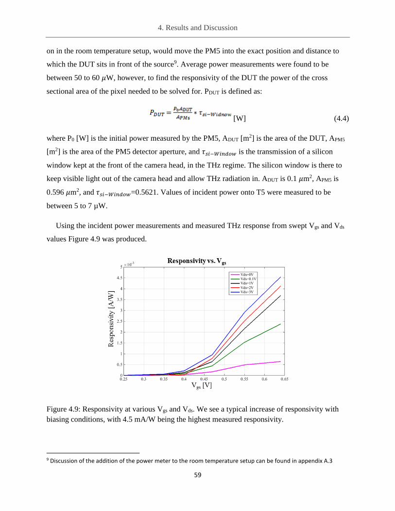
4. Results and Discussion
59
on in the room temperature setup, would move the PM5 into the exact position and distance to
which the DUT sits in front of the source9. Average power measurements were found to be
between 50 to 60 𝜇W, however, to find the responsivity of the DUT the power of the cross
sectional area of the pixel needed to be solved for. PDUT is defined as:
[W] (4.4)
where P0 [W] is the initial power measured by the PM5, ADUT [m2] is the area of the DUT, APM5
[m2] is the area of the PM5 detector aperture, and 𝜏𝑠𝑖−𝑊𝑖𝑛𝑑𝑜𝑤 is the transmission of a silicon
window kept at the front of the camera head, in the THz regime. The silicon window is there to
keep visible light out of the camera head and allow THz radiation in. ADUT is 0.1 𝜇m2, APM5 is
0.596 𝜇m2, and 𝜏𝑠𝑖−𝑊𝑖𝑛𝑑𝑜𝑤=0.5621. Values of incident power onto T5 were measured to be
between 5 to 7 µW.
Using the incident power measurements and measured THz response from swept Vgs and Vds
values Figure 4.9 was produced.
Figure 4.9: Responsivity at various Vgs and Vds. We see a typical increase of responsivity with
biasing conditions, with 4.5 mA/W being the highest measured responsivity.
9 Discussion of the addition of the power meter to the room temperature setup can be found in appendix A.3

4. Results and Discussion
60
Work in [37] noted a trend where responsivity could be increased up to 2-4 times when in
deep saturation. In Figure 4.9 there is a 9x jump in responsivity from Vds=0 V to Vds=3 V, and a
2x jump from Vds=0.1 V to Vds=3.0 V. Figure 4.9's slowing rate of increase with higher drain
bias matches that of work in [54]. It must be noted, that unlike [54], at Vds=0 V the setup shorts
drain to ground; this is not an open drain setup. For comparison to the values in Figure 4.9, work
from [32] roughly estimates that an internal current responsivity from 0.35 µm CMOS n-
MOSFETs can be as high as ~21 A/W at room temperature. Using the estimated parameters in
[32], calculated responsivity can also be as low as 0.5 mA/W in an open drain configuration at
~77GHz. Compared to other technologies, work done on InGaAs HEMTs in [20] showed current
responsivity to be ~5 A/W with incident radiation of 460 GHz. While a comparison of expected
internal current responsivity for SBDs in [56] were expected to be ~15 A/W. When the resistance
at Vth (measured as 1 MΩ in section 4.1.3) is applied to the responsivity in Figure 4.9 at
Vgs=0.64 V, the responsivity is calculated to be 4.5 kV/W. This is similar to the 103 V/W values
of SBDs in table 1.2, but smaller than the highest responsivity of microbolometers (107 V/W). It
should be noted that the high responsivity of 107 V/W was obtained by LETI for frequencies of
2.7 THz [6]. For many other works that use microbolometers in the sub-THz range, the
responsivities tend to be lower. An example would be in works of [64], Nb5N6 microbolometers
were found to have RF responsivity of 480 V/W at a frequency of 0.28 THz.
From the responsivity calculated in Figure 4.9, NEP can then also be calculated. NEP is seen
as the minimum of incident power a device can detect over the noise spectral density. NEP is
seen as:
𝑁𝐸𝑃 =𝑆𝑣𝐼
𝑅𝐼 [
𝑊
√𝐻𝑧] (4.5)
where RI is the responsivity in A/W calculated and found from equation 4.3 and Figure 4.9, and
SVI is the noise spectral density in A/√𝐻𝑧. For SVI Figure 4.5 from section 4.1.4 was used.

4. Results and Discussion
61
Figure 4.10: NEP measured using the Responsivity from Figure 4.9, and noise measurements
from the spectrum analyzer.
Figure 4.10 indicates that 6 -7 nW/√Hz is the lowest NEP for T5 for Vds=0.1 V and up. For a
Vds=3.0 V (our normal biasing condition for room and varying temperature setups), the NEP at
peak responsivity was found to be 80 – 100 nW/√Hz. While responsivity has been shown to
increase with an increase in drain bias current, it also causes an increase in 1/f noise, thereby an
unfortunate increase in NEP. This is the reason that, while T5 may have its highest responsivity
at threshold, its NEP is larger than expected (see table 1.2) and makes THz DC rectification more
difficult to detect.
If shot noise limited detection were achieved, calculations (using section 4.1.4 shot noise
values) of the NEP would be the values listed in Table 4.4.
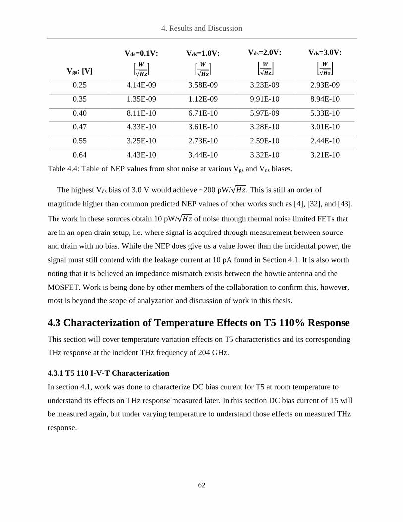
4. Results and Discussion
62
Vgs: [V]
Vds=0.1V:
[𝑾
√𝑯𝒛]
Vds=1.0V:
[𝑾
√𝑯𝒛]
Vds=2.0V:
[𝑾
√𝑯𝒛]
Vds=3.0V:
[𝑾
√𝑯𝒛]
0.25 4.14E-09 3.58E-09 3.23E-09 2.93E-09
0.35 1.35E-09 1.12E-09 9.91E-10 8.94E-10
0.40 8.11E-10 6.71E-10 5.97E-09 5.33E-10
0.47 4.33E-10 3.61E-10 3.28E-10 3.01E-10
0.55 3.25E-10 2.73E-10 2.59E-10 2.44E-10
0.64 4.43E-10 3.44E-10 3.32E-10 3.21E-10
Table 4.4: Table of NEP values from shot noise at various Vgs and Vds biases.
The highest Vds bias of 3.0 V would achieve ~200 pW/√𝐻𝑧. This is still an order of
magnitude higher than common predicted NEP values of other works such as [4], [32], and [43].
The work in these sources obtain 10 pW/√𝐻𝑧 of noise through thermal noise limited FETs that
are in an open drain setup, i.e. where signal is acquired through measurement between source
and drain with no bias. While the NEP does give us a value lower than the incidental power, the
signal must still contend with the leakage current at 10 pA found in Section 4.1. It is also worth
noting that it is believed an impedance mismatch exists between the bowtie antenna and the
MOSFET. Work is being done by other members of the collaboration to confirm this, however,
most is beyond the scope of analyzation and discussion of work in this thesis.
4.3 Characterization of Temperature Effects on T5 110% Response
This section will cover temperature variation effects on T5 characteristics and its corresponding
THz response at the incident THz frequency of 204 GHz.
4.3.1 T5 110 I-V-T Characterization
In section 4.1, work was done to characterize DC bias current for T5 at room temperature to
understand its effects on THz response measured later. In this section DC bias current of T5 will
be measured again, but under varying temperature to understand those effects on measured THz
response.

4. Results and Discussion
63
Figure 4.11: Measured DC Bias Current without THz at temperatures of 294, 180, 150, 140, 130
Kelvin.
In Figure 4.11, we see close agreement with works like [33] and [53] where Ids changes more
in the subthreshold region with temperature than it does in the superthreshold region. It is
expected for drain-source current in the linear and saturation regions to increase with a decrease
in temperature after reaching a high enough Vgs [53] [55]. This is supported by [26], which states
electron mobility in strong inversion mode changes its dependence from T-1.5 to T-2 with decrease
in temperature. Equations 2.3 and 2.4 also agree with the increase in current in the linear-
saturation region. However, more work was done in this project to characterize the subthreshold
and threshold regions, therefore, Vgs was not biased high enough to observe the linear and
saturated region effects. The subthreshold region expects diffusion to decrease as per the
exponential dependence on temperature in Equation 2.1, where S, VT, and Vth all have
temperature dependencies. S is then extrapolated from the different temperature curves in Figure
4.11 using the inverse slope method. The values of the extrapolated S vs temperature is listed in
Table 4.5.
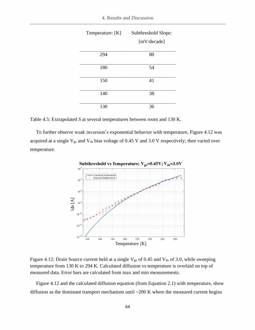
4. Results and Discussion
64
Temperature: [K] Subthreshold Slope:
[mV/decade]
294 80
180 54
150 41
140 38
130 36
Table 4.5: Extrapolated S at several temperatures between room and 130 K.
To further observe weak inversion’s exponential behavior with temperature, Figure 4.12 was
acquired at a single Vgs and Vds bias voltage of 0.45 V and 3.0 V respectively; then varied over
temperature.
Figure 4.12: Drain Source current held at a single Vgs of 0.45 and Vds of 3.0, while sweeping
temperature from 130 K to 294 K. Calculated diffusion vs temperature is overlaid on top of
measured data. Error bars are calculated from max and min measurements.
Figure 4.12 and the calculated diffusion equation (from Equation 2.1) with temperature, show
diffusion as the dominant transport mechanism until ~200 K where the measured current begins
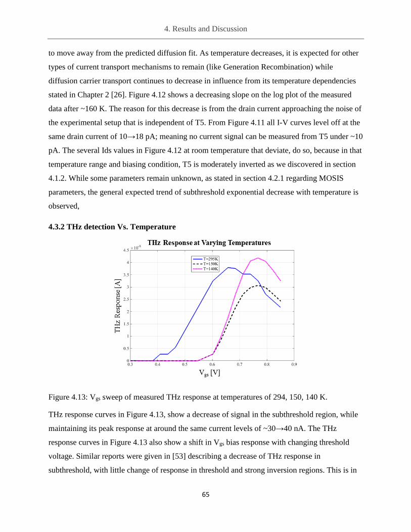
4. Results and Discussion
65
to move away from the predicted diffusion fit. As temperature decreases, it is expected for other
types of current transport mechanisms to remain (like Generation Recombination) while
diffusion carrier transport continues to decrease in influence from its temperature dependencies
stated in Chapter 2 [26]. Figure 4.12 shows a decreasing slope on the log plot of the measured
data after ~160 K. The reason for this decrease is from the drain current approaching the noise of
the experimental setup that is independent of T5. From Figure 4.11 all I-V curves level off at the
same drain current of 10→18 pA; meaning no current signal can be measured from T5 under ~10
pA. The several Ids values in Figure 4.12 at room temperature that deviate, do so, because in that
temperature range and biasing condition, T5 is moderately inverted as we discovered in section
4.1.2. While some parameters remain unknown, as stated in section 4.2.1 regarding MOSIS
parameters, the general expected trend of subthreshold exponential decrease with temperature is
observed,
4.3.2 THz detection Vs. Temperature
Figure 4.13: Vgs sweep of measured THz response at temperatures of 294, 150, 140 K.
THz response curves in Figure 4.13, show a decrease of signal in the subthreshold region, while
maintaining its peak response at around the same current levels of ~30→40 nA. The THz
response curves in Figure 4.13 also show a shift in Vgs bias response with changing threshold
voltage. Similar reports were given in [53] describing a decrease of THz response in
subthreshold, with little change of response in threshold and strong inversion regions. This is in

4. Results and Discussion
66
contrast to many GaAs FETs that increase in THz response with a decrease in temperature, as
see in works of [6] [38] [53] and [56], while also having a narrower detection peak with
decreasing temperature. Further evaluation of peak signal at shifting threshold will be given in
section 4.3.3.
Figure 4.14 shows the THz response held under multiple subthreshold Vgs biasing conditions
at a Vds=3.0V, while sweeping temperature from room to 130 K.
Figure 4.14: THz signal current held at multiple Vgs bias in subthreshold, at Vds=3.0 V, for
varying temperatures of 295 → 130 K.
Measurement of subthreshold response vs temperature in Figure 4.14, indicates that not only
does T5 see an almost linear decrease of THz response on a semi-log plot, but the rate of
decrease in THz response grows smaller the larger Vgs becomes. From 250 to 160 K, Vgs=0.45 V
decreases by ~2 orders of magnitude, while for Vgs=0.56 V there is a ~1.5 order magnitude
decrease.

4. Results and Discussion
67
Figure 4.15: Measured THz response at Vgs=0.45, 0.56 V, Vds=3.0 V and their corresponding
Drain-Source Current with varying temperature.
To determine if the DC current (with THz source off) showed any similarity to the THz
response behavior in the subthreshold with decreasing temperature, Figure 4.15 was assembled.
Figure 4.15 shows that while both the DC current and THz response do decrease faster with
decreasing Vgs, they do not decrease at the same rate. At 295 K the DC currents at different Vgs
are 1 order of magnitude apart, the THz responses a factor of ~7; while at 130 K the DC current
curves are 2 orders of magnitude apart, the THz response at 3 orders of magnitude apart. Figure
4.15 also shows that regardless of Vgs, DC current and THz response curves remain parallel to
each other with decreasing temperature. At room temperature, DC current and THz response for
both Vgs are ~2 orders of magnitude apart, and at 130 K they remain ~2 orders of magnitude
apart. It is important to note that this is happening while Figure 4.12 shows the Vgs = 0.45 V
curve to change dominant carrier transport with decreasing temperature.
In section 4.1.4 it was noted that T5 NEP was dominated by 1/f, however, it is known that 1/f
decreases with a decrease in temperature [55]. It was expected for responsivity to rise (from
maintained drain biasing) and NEP to fall from decrease in 1/f. From Figures 4.13 and 4.14 the
THz response with varying temperature did not match the expectation. However, it was
discussed in Section 4.2.3 that with increasing drain current comes an increase in responsivity as
well as increase in NEP from 1/f. It was found that with a decrease in drain-source current from

4. Results and Discussion
68
Figure 4.11, there was a decrease in THz response measured in Figures 4.13, 4.14, and 4.15.
Whereas, for threshold THz response, drain-source current does not seem to decrease by much
and neither does responsivity. More on threshold biasing response will be discussed in Section
4.3.3.
4.3.3 Peak Response at Vth vs. Temperature
In sections 4.2.1 and 4.3.2 it was observed that at room temperature, peak THz response
appeared around threshold voltage, and discussed how works like [53] showed similar
dependencies of peak response to threshold voltage. In this section, peak THz response is
measured in relation to the temperature dependency of the MOSFET threshold voltage and drain-
source bias current at that threshold bias.
Using the ELR method from section 4.1.1, threshold voltage from the curves in Figure 4.11
were extrapolated for the temperatures of 294, 180, 150, 140, 130 K. The extrapolated threshold
voltages were then used with Equation 2.6 to calculate threshold voltages across a sweeping
range of temperature between room and 130 K. Then the Vth values were plotted in Figure 4.16
to observe where peak THz response would occur relative to Vth with temperature.
Figure 4.16: Most peak signal occurs at or just above the threshold voltage calculated by
Equation 2.6. However, peak shifts at relatively the same linear rate as the threshold voltage with
temperature.

4. Results and Discussion
69
Figure 4.17: Peak THz Response with respect to its corresponding DC bias current. Peak THz
current signals occur at ~10 µA. Error bars are calculated using min and max measured THz
response.
Figure 4.16 shows most THz response peaks were measured at or above threshold voltage at a
consistent rate, indicating a relation between threshold voltage and peak THz current regardless
of temperature. Work from [53] and [39] mentions similar results where peak follows the
threshold voltage shift with temperature. For further understanding THz peak response at
changing Vth with temperature, THz peak response was plotted alongside DC bias current at their
corresponding temperatures in Figure 4.17.
Figure 4.17 shows that peak THz response stays relatively the same regardless of temperature
which is in agreement with the work found in [53], where peak THz response seems to hover
around the same magnitude. However, work in [61] shows the opposite response, in that THz
peak increases with decreasing temperature, with an exponential increase after 120 K. Figure
4.17 only measures temperatures of up to 130 K, therefore, whether the THz peak response
would suddenly increase sharply after 120 K and below is unknown. While [61] did measure
channel conductance, there is no indication that a large drain bias was applied similar to the
Vds=3.0 V that was used to obtain Figure 4.17. Work found in [39] reports a different peak THz
response with temperature found in Figure 4.17. The work in [39] measured a continuing drop in
THz response due to poor performance of silicon at cryogenic temperatures.
4. Results and Discussion
70
It is also interesting to note how in Figure 4.17, the peak THz response occurs at the same DC
drain-source bias current regardless of temperature. For room temperature, Figure 4.8 showed
the peak at 10 µA, and as temperature is swept from room to 130 K in Figure 4.17, all THz
response peaks occur around 10 µA. Whereas, in subthreshold mode, diffusion current transport
decreases with temperature as shown in figure 4.11, and it’s corresponding THz response
decreases as shown in Figure 4.14. This was shown in detail in Figure 4.15, where both DC bias
current and THz response decreased at relatively the same rate with decrease in temperature.
From Figures 4.15 and 4.17, it can be inferred that there is some dependence on the DC drain-
source bias current and the measured THz response.
71
5. Conclusion
This work’s focus was to optimize Si-MOSFETs for use in making a THz Si-CMOS FPA
sensitive enough for standoff detection. A standoff THz FPA would be invaluable in a multitude
of applications including medical, security, earth sciences, communication and industry. The
desire was to optimize the MOSFET in a way that highlights the benefits of this technology
while outweighing the trade-offs compared of competing technologies like bolometers and
Schottky Diodes. Since THz detection and frequency depend on gate length and MOSFET
geometry, using a bowtie antenna, 2 µm source extension, and 350 nanometer gate length, that
detection could be achieved with high responsivity and low NEP at the THz frequency of ~200
GHz. To further optimize THz detection in the MOSFET, the THz detection mechanisms under
different biasing conditions were examined.
To carry out the work, a low noise experimental setup was created to filter out as much
outside interference as possible. A lock-in amplifier was used in the detection of the AC induced
drain current from the incident THz radiation. At the same time DC drain-source bias current
was measured to observe the effects of detection from drain current enhancement. The low noise
test setup utilized battery operated voltage sources to ensure no extra ground noise entered the
biasing part of the MOSFET circuit. A low noise current to voltage preamplifier was used to
enhance any current signal measured out of the MOSFET. Finally, to ensure no added noise
interference, a low noise steel enclosure was created to shield a fanout board, which routed the
test devices on the GEN2 chip to its corresponding separate circuits of detection, biasing, and
other.
THz radiation at ~200 GHz was measured by the Si-MOSFET, T5. System noise (in the form
of 1/f noise) led to the inability to measure DC rectified THz response current from the
MOSFET. Predicted plasmonic and thermionic detection mechanisms were calculated but
showed different behavior from the AC measurement depending on biasing conditions. The
predicted thermionic response was calculated to be higher than the AC measurements, however,
this would have led to a measurement of DC rectification current. The peak THz response was
also found to be at or above threshold voltage, this does not follow the thermionic emission
model prediction that peak response occurs in the subthreshold region. Responsivity and NEP
were found to be at best 4.5 mA/W and 6 nW/√Hz respectively depending on biasing conditions.
5. Conclusion
72
While the peak responsivity proved to be consistent with Table 1.2, and on the same level with
its competing technology of SBDs, it was still lower than its other competing technology of
microbolometers (depending on frequency of operation). T5's NEP, however, proved to be on the
same level as microbolometers, when shot noise limited. It is believed that higher responsivity is
possible, however, an impedance mismatch between the antenna and the MOSFET lowered the
responsivity. The higher NEP compared to other works utilizing Si-MOSFETs was thought to be
from the presence of the large 1/f noise, known to occur under large drain biasing conditions.
Properties of the MOSFET were characterized such as its induced DC drain-source bias current
(Ids) and its noise power spectrum. It was found that the MOSFET operated within normal range
of other MOSFETs including its bias current in the subthreshold and superthreshold regions.
However, it's noise characteristics showed 1/f to be at nearly the same level as the AC induced
THz detection signal. Since 1/f is inherent to all CMOS processes and is known to increase under
heavy bias it was not possible to have Ids enhancement without the increase of 1/f.
To better characterize the THz detection, T5 was cooled down to down to 130 Kelvin to
observe the AC THz response on the gate with its corresponding DC drain-source behavior. It
was found that although THz response decreased with temperature in the subthreshold region it
remained relatively the same at just above threshold bias regardless of temperature. The DC
drain-source current (Ids) from the MOSFET was also measured under the same temperature
conditions and found to operate in agreement with other works using Si-MOSFETs under
decreasing temperature conditions. The temperature data under the different biasing conditions
showed the THz response to have a strong relation to the DC Ids. The first indication of this are
the measurements in the subthreshold region, which showed both the THz response and DC Ids
decrease at an exponential rate with decreasing temperature. The rate of decrease for THz
response and DC Ids with decreasing temperature also went down with increasing Vgs. The
second indication are the measurements showing that both the peak THz response and DC Ids do
not change with decreasing temperature of room to 130 K. With every peak THz response
measurement (at 10 nA) was an observed ~10 µA of DC Ids.
Threshold voltage was measured and calculated with change in temperature and was found to
increase with decreasing temperature. As temperature was decreased, it was observed that peak
THz response consistently occurred at just above threshold voltage at a rate following the

5. Conclusion
73
increase of threshold voltage with temperature. This consistency in peak occurring above
threshold regardless of temperature is a mark against the validity of the thermionic emission
model which indicated that peak would occur in subthreshold.
5.1 Future work
This modified Si-MOSFET (T5) has an expected responsivity (compared to other works), high
NEP, and a circuit too noisy to measure accurately the DC rectified THz response. Future steps
will be taken to better account for all these factors by further optimizing the MOSFET and
experimental setup. To improve responsivity more FTDT analysis of antenna response to THz
frequencies will be done. By better understanding the how the bowtie antenna couples the THz
radiation to the MOSFET gate and source regions better coupling configurations can be made to
increase the responsivity. It has been found in works such as [57] and [58], that by thinning the
substrate of the MOSFET, responsivity can also be improved. The work in [57] found that by
thinning the substrate by a ~1/2, it is possible to measure an order of magnitude improvement in
responsivity. Therefore, future MOSFETs are being thinned to measure this increase in
responsivity with decrease in substrate thickness.
To decrease NEP T5 must overcome the 1/f noise inherent to the CMOS process. One
method to accomplish this is to undergo a cleaner CMOS fabrication to lessen the number of
defects in the MOSFET channel. The other method is to modulate (or chop) the incident THz
radiation at a higher frequency above the 1/f. As our current-to-voltage preamplifier does not
allow any higher modulation of signal with its low bandwidths at the desired gains of around
10-10 A/V, the SR560 voltage preamplifier will. Any gain added to the THz response will be
moved into the camera head by placing an op-amp directly after the MOSFET. By putting gain
onto the THz response immediately after detection, the signal will be enhanced to a higher level
than any external noise entering the circuit later. Adding an op-amp for a single MOSFET can be
seen as the next logical step in a CMOS FPA.

5. Conclusion
74
Figure 5.1: This image shows GEN4 with 29 new test structures, each varying in source
extension length, antenna coupling configurations, and dipole antenna configurations.
It is still a goal to better optimize detection of THz at 200 GHz and other atmospheric window
frequencies, therefore another generation of chip will be made (nicknamed GEN4) that will vary
the source region geometry to other various lengths. Since GEN1 and GEN2 chips showed an
increase of response with an increase in source extension, it is desired to know at what length of
source extension will the THz response stop increasing. Conceivably the source extension also
affects the frequency response of the MOSFET. A GDS image of GEN4 is showed in Figure 5.1.
While GEN2 and the Si-MOSFET T5 (with 2 µm source extension) yielded an average
responsivity and high NEP, it is hoped that the next generation of low noise test setup and
optimized MOSFET parameters will yield better results for a standoff FPA in the THz regime.
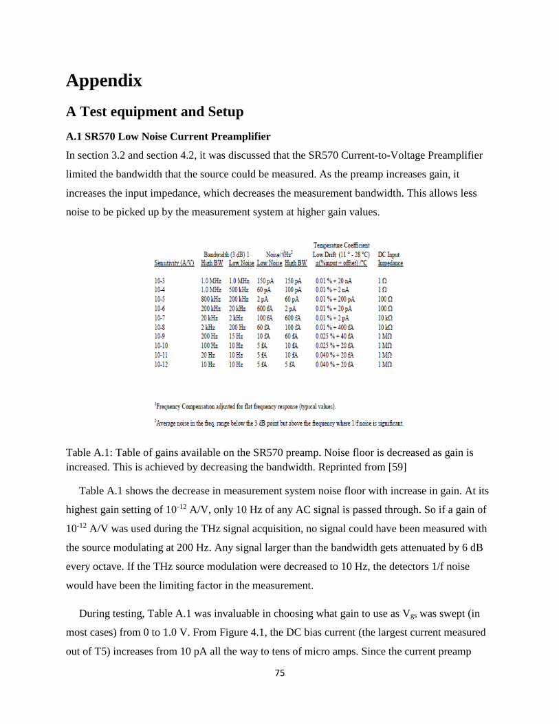
75
Appendix
A Test equipment and Setup
A.1 SR570 Low Noise Current Preamplifier
In section 3.2 and section 4.2, it was discussed that the SR570 Current-to-Voltage Preamplifier
limited the bandwidth that the source could be measured. As the preamp increases gain, it
increases the input impedance, which decreases the measurement bandwidth. This allows less
noise to be picked up by the measurement system at higher gain values.
Table A.1: Table of gains available on the SR570 preamp. Noise floor is decreased as gain is
increased. This is achieved by decreasing the bandwidth. Reprinted from [59]
Table A.1 shows the decrease in measurement system noise floor with increase in gain. At its
highest gain setting of 10-12 A/V, only 10 Hz of any AC signal is passed through. So if a gain of
10-12 A/V was used during the THz signal acquisition, no signal could have been measured with
the source modulating at 200 Hz. Any signal larger than the bandwidth gets attenuated by 6 dB
every octave. If the THz source modulation were decreased to 10 Hz, the detectors 1/f noise
would have been the limiting factor in the measurement.
During testing, Table A.1 was invaluable in choosing what gain to use as Vgs was swept (in
most cases) from 0 to 1.0 V. From Figure 4.1, the DC bias current (the largest current measured
out of T5) increases from 10 pA all the way to tens of micro amps. Since the current preamp
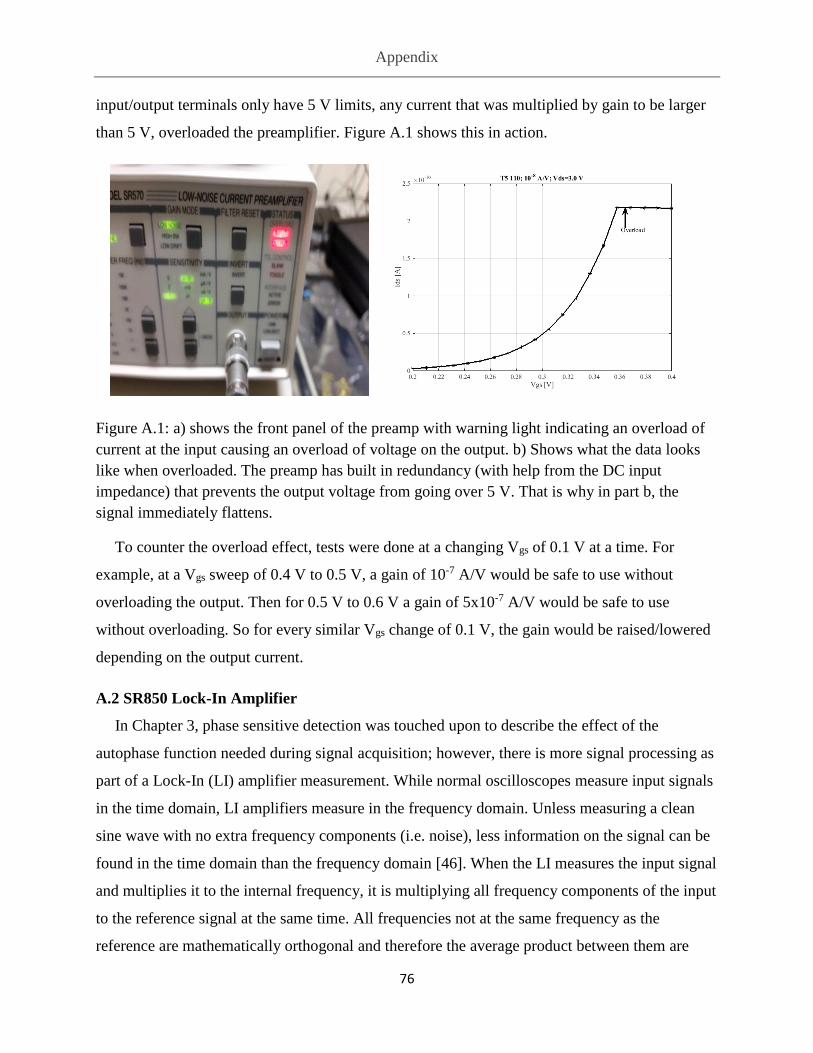
Appendix
76
input/output terminals only have 5 V limits, any current that was multiplied by gain to be larger
than 5 V, overloaded the preamplifier. Figure A.1 shows this in action.
Figure A.1: a) shows the front panel of the preamp with warning light indicating an overload of
current at the input causing an overload of voltage on the output. b) Shows what the data looks
like when overloaded. The preamp has built in redundancy (with help from the DC input
impedance) that prevents the output voltage from going over 5 V. That is why in part b, the
signal immediately flattens.
To counter the overload effect, tests were done at a changing Vgs of 0.1 V at a time. For
example, at a Vgs sweep of 0.4 V to 0.5 V, a gain of 10-7 A/V would be safe to use without
overloading the output. Then for 0.5 V to 0.6 V a gain of 5x10⁻⁷ A/V would be safe to use
without overloading. So for every similar Vgs change of 0.1 V, the gain would be raised/lowered
depending on the output current.
A.2 SR850 Lock-In Amplifier
In Chapter 3, phase sensitive detection was touched upon to describe the effect of the
autophase function needed during signal acquisition; however, there is more signal processing as
part of a Lock-In (LI) amplifier measurement. While normal oscilloscopes measure input signals
in the time domain, LI amplifiers measure in the frequency domain. Unless measuring a clean
sine wave with no extra frequency components (i.e. noise), less information on the signal can be
found in the time domain than the frequency domain [46]. When the LI measures the input signal
and multiplies it to the internal frequency, it is multiplying all frequency components of the input
to the reference signal at the same time. All frequencies not at the same frequency as the
reference are mathematically orthogonal and therefore the average product between them are
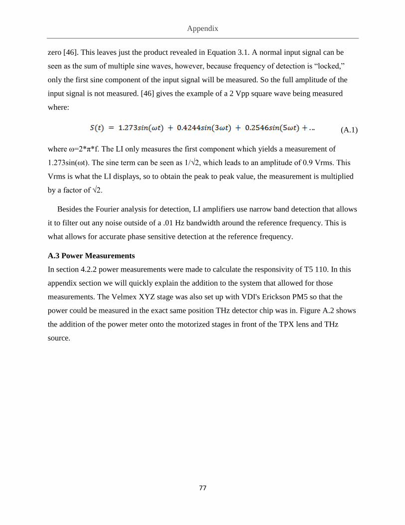
Appendix
77
zero [46]. This leaves just the product revealed in Equation 3.1. A normal input signal can be
seen as the sum of multiple sine waves, however, because frequency of detection is “locked,”
only the first sine component of the input signal will be measured. So the full amplitude of the
input signal is not measured. [46] gives the example of a 2 Vpp square wave being measured
where:
(A.1)
where ω=2*π*f. The LI only measures the first component which yields a measurement of
1.273sin(ωt). The sine term can be seen as 1/√2, which leads to an amplitude of 0.9 Vrms. This
Vrms is what the LI displays, so to obtain the peak to peak value, the measurement is multiplied
by a factor of √2.
Besides the Fourier analysis for detection, LI amplifiers use narrow band detection that allows
it to filter out any noise outside of a .01 Hz bandwidth around the reference frequency. This is
what allows for accurate phase sensitive detection at the reference frequency.
A.3 Power Measurements
In section 4.2.2 power measurements were made to calculate the responsivity of T5 110. In this
appendix section we will quickly explain the addition to the system that allowed for those
measurements. The Velmex XYZ stage was also set up with VDI's Erickson PM5 so that the
power could be measured in the exact same position THz detector chip was in. Figure A.2 shows
the addition of the power meter onto the motorized stages in front of the TPX lens and THz
source.

Appendix
78
Figure A.2: Shows the room temperature setup from Figure 3.6 with the addition of the Erikson
PM5 power meter. The stages move along the XYZ axis with a 6.5 micron stepping size to move
the meter into the exact position the DUT was at prior. This image also includes the TPX lens.
Over the course of 12 hours, the VDI THz source varied in power by 2. So power was taken
with the PM5 at the beginning and end of a measurement session, where a typical session ranged
from 5 to 8 hours. The PM5 meter was also used to characterize the THz source beam. It was
through the PM5 measurements that it was determined that a TPX lens would be useful in
collimating the beam to create an equal power distribution across the test chip.
A.4 Noise System Analysis
Chapter 3 discusses the low noise experimental setup, and while the instruments aided in
filtering out noise, much more work was performed on optimizing the grounding scheme to
further decrease the system noise inherent in the setup. One of the largest problems was 60 Hz
noise as Figure A.3 will show.
Camera CAN w/Chip
PM5 Calibrated Detector
TPX Lens
THz Source

Appendix
79
Figure A.3: Many of the spikes, are 60 Hz noise, in that they occur every multiple of 60. This
figure has the additional benefactor, that for every gain setting, the noise of T5 remains above the
Preamplifier’s noise floor.
To obtain the noise figures showed in Figure 4.5 from Figure A.3, the first thing that was
done, was to eliminate any grounding noise present in the system. One potential reason for all of
the 60 Hz noise are ground loops, when ground lines from multiple points all lead up to the same
circuit. To avoid this, the ground for every instrument chassis and circuit, was all rooted through
a single conductor back to the computer then to a SOLA HD power conditioner plugged into the
wall designed to filter 60 Hz noise. The power conditioner attenuates the noise by 120 dB to 60
dB depending on the mode of operation.
Another method to keep out low frequency noise was the low noise box designed to house the
jumper board to switch between test structurers of GEN2. Figure A.4 shows the inside of the low
noise box.

Appendix
80
Figure A.4: Shows the inside of the LNB, with its corresponding jumpers to control bias and
signal readouts from the desired MOSFET.
The LNB was designed to filter out EM frequencies of 60 Hz and up, to prevent the signal
traveling through the line from picking it up. Protocase Inc., was used to help make and build the
design. The overlap on the edges of the box, was designed to attenuate the EM frequencies that
made it through the lid. The material is 3 mm of cold rolled steel (CRS), a material used in many
RF shielding applications, and is known for being a good option when materials like aluminum
do not block low enough frequencies [60]. The 3 mm CRS was also chosen in consideration for
skin depth, an important parameter when shielding against higher frequencies as well as low
frequencies [50]. Lastly to ensure the case acted as a Faraday cage, the ground line was attached
to the LNB chassis.
B MATLAB Code
This section of the appendix includes the Matlab 2014b code written to conduct the automatic
testing described in section 3.3 from instrument connection and commands to data display. All
experiments performed in this thesis utilized some variation of the following 4 codes: Vgs sweep,
Vds sweep for resistance channel measurement, temperature sweep (take data while temperature
warms back up to room), and power measurement with the VDI calibrated power meter. Code to
connect to and from devices were created by Kenny Fourspring from Harris Corporation, while
data display and various other changes were done by Katie Seery and Jack Horowitz.

Appendix
81
Vgs Sweep Code
%Created by: Kenny Fourspring 10-25-2015
%edits: Katie Seery & Jack Horowitz
%harris inc------------------------------------------------------------
%LAIR-------------------------------------------------------------------
%Test code created to sweep Vgs at a single Vds.
[mainframeComPort,srsComPort, shutterComPort,stageComPort] = define_comports();
%Defines connection ports for instruments.
%-configuration variables-------------------------------------------------
testnum=testnum+1;
teststruct='Gen2';
d=date;
da=datestr(datenum(d,'dd-mmm-yyyy'),'mmddyyyy');
string='T5_05to060';
gainFactor=1*10^-6; %A/V
Vds =3.0;
VgsStart = 0.5;
VgsEnd = 0.6;
nVgs =10.0;
VgsSettleTime =8; %seconds
shutterDelay = 0.10;%seconds
gain=CorrectGain(gainFactor); %Function to change gainFactor to a number, to give to Preamp.
objP=srsPre_open('COM19',gain) %Sends command to change gain of preamplifier.
%srs freqency stuff-------------------------------------------------------
refFreq = 170; % reference frequency in Hz.
%refPhase = 0;
LIsens=0.02; %V %Sets LI sensitivity
modeName = 'external';
scanLenSec = 1;
sampRate = 13; %10 = 64 Hz %don’t use 10
scanMode = 'shot' ; %valid values are loop and shot
%calcualte voltages--------------------------------------------------------
VgsInc = (VgsEnd - VgsStart)./(nVgs-1);
if nVgs == 1
vtgsMat = VgsStart;
else
VgsMat = VgsStart:VgsInc:VgsEnd;
end
%setup the SRS lockin ----------------------------------------------------
objS=srs_open(srsComPort);
srs_set_sensitiviy(objS,LIsens); %Sets Lock-In Sensitivity
srs_set_ref_freq(objS,refFreq); %Sets reference Frequency
%srs_set_ref_phase(objS,refPhase); %Sets reference Phase
srs_auto_phase(objS); % auto phase at the start of each measurement
srs_set_ref_mode(objS,modeName) %Sets reference mode
srs_setup_traces(objS) %Sets up traces
Appendix
82
sampRateVal=srs_set_sample_rate(objS,sampRate); %Sets sample rate-from fn.
srs_set_scan_mode(objS,scanMode); %Sets scan mode
srs_set_scan_len(objS,scanLenSec); %Sets scan time?
%chanel #l 3.3, channel #4 = Vds, #8 Vgs-------------------------------------
[mainframeObj] = mainframe_open_connection(mainframeComPort);
mainframe_reset_powersupplies(mainframeObj); %reset power supplies
mainframe_set_voltage(mainframeObj,1,3.3)
mainframe_output_on(mainframeObj,1) % tun output on
mainframe_set_voltage(mainframeObj,4,Vds)%set DRAIN voltage
mainframe_output_on(mainframeObj,4) % tun drain output on
objShutter=shutter_open_connection(shutterComPort);
shutter_open(objShutter)
for vCount = 1:nVgs
%take measurmenet with shutter open as reference
mainframe_set_voltage(mainframeObj,8,VgsMat(vCount))%set GATE voltage
mainframe_output_on(mainframeObj,8) % turn output on
pause(VgsSettleTime)
%---------------------------------------------------------------------
srs_clear_all(objS); % clears all data out of srs
nPts = srs_get_npts(objS); %make sure buffer is cleared
srs_start(objS);
disp('running test.....')
pause(scanLenSec+1);
disp('done running test')
srs_pause(objS);
nPts = srs_get_npts(objS);
% nPts=33
traceDataOpen(:,:,vCount) = srs_get_data_ascii(objS,nPts);
%----------------------------------------------------------------------
mainframe_output_off(mainframeObj,8) %turn off gate
%---------------------------------------------------------------------
%take measurement with shutter closed
shutter_close(objShutter)
pause(shutterDelay)
mainframe_set_voltage(mainframeObj,8,VgsMat(vCount))%set GATE voltage
mainframe_output_on(mainframeObj,8) % turn output on
pause(VgsSettleTime)
srs_clear_all(objS); % clears all data out of srs
nPts = srs_get_npts(objS);
srs_start(objS);
disp('running test.....')
pause(scanLenSec+1);

Appendix
83
disp('done running test')
srs_pause(objS);
nPts = srs_get_npts(objS);
traceDataClosed(:,:,vCount) = srs_get_data_ascii(objS,nPts); %puts data from specified inputs
(LI/DC) into traces.
shutter_open(objShutter)
mainframe_output_off(mainframeObj,8) %turn off gate
end
mainframe_output_off(mainframeObj,4) %turn off Vds
%Data Reduction
traceData=traceDataOpen-traceDataClosed;
mainframe_output_off(mainframeObj,1) %turn off 3.3
mainframe_close_connection(mainframeObj);
shutter_close_connection(objShutter)
%% AC DATA FIGURES
%Compiles Figure for AC measurement of THz induced current in MOSFET
%channel in the LIs rms units
str=sprintf('T5 110 %.0f GHz %0.5e AV Vds=%f',freq,gainFactor,Vds);
figure;
meanVolts = zeros(nVgs,3);
for vCount = 1:nVgs
curVgs = zeros(nPts(1),1);
curVgs(:) = VgsMat(vCount);
plot(curVgs,traceDataOpen(:,3,vCount)*gainFactor,'*r')
hold on
plot(curVgs,traceDataClosed(:,3,vCount)*gainFactor,'*b')
hold on
plot(curVgs,traceData(:,3,vCount)*gainFactor,'*k')
meanVolts(vCount,1) = mean(traceDataOpen(:,3,vCount));
meanVolts(vCount,2) = mean(traceDataClosed(:,3,vCount));
meanVolts(vCount,3) = mean(traceDataOpen(:,3,vCount))-
mean(traceDataClosed(:,3,vCount));
end
plot(VgsMat,meanVolts(:,1)*gainFactor,'-r')
plot(VgsMat,meanVolts(:,2)*gainFactor,'-b')
plot(VgsMat,meanVolts(:,3)*gainFactor,'-k')
title(str)
xlabel('Vgs (V)')
ylabel('Measured Ids (A_r_m_s)')
filenamefigs=sprintf('C:\\Users\\A270-
THz\\Dropbox\\kennys_thz_matlab\\Tests\\%s\\%s\\figures\\Test%d__AC%.0fGHz_gain%.0d_
%s',da,teststruct,testnum,freq,gainFactor,string);

Appendix
84
savefig(filenamefigs)
%% AC Correction DATA FIGURES
%Compiles Figure for AC measurement of THz induced current in MOSFET
%channel with peak-peak signal
str=sprintf('T5 110 %.0f GHz %0.5e AV Vds=%f Correction',freq,gainFactor,Vds);
figure;
meanVolts = zeros(nVgs,3);
for vCount = 1:nVgs
curVgs = zeros(nPts(1),1);
curVgs(:) = VgsMat(vCount);
plot(curVgs,traceDataOpen(:,3,vCount)*gainFactor/(2/pi*1/sqrt(2)),'*r')
hold on
plot(curVgs,traceDataClosed(:,3,vCount)*gainFactor/(2/pi*1/sqrt(2)),'*b')
hold on
plot(curVgs,traceData(:,3,vCount)*gainFactor/(2/pi*1/sqrt(2)),'*g')
meanVolts(vCount,1) = mean(traceDataOpen(:,3,vCount));
meanVolts(vCount,2) = mean(traceDataClosed(:,3,vCount));
meanVolts(vCount,3) = mean(traceDataOpen(:,3,vCount))-
mean(traceDataClosed(:,3,vCount));
end
plot(VgsMat,meanVolts(:,1)*gainFactor/(2/pi*1/sqrt(2)),'-r')
plot(VgsMat,meanVolts(:,2)*gainFactor/(2/pi*1/sqrt(2)),'-b')
plot(VgsMat,meanVolts(:,3)*gainFactor/(2/pi*1/sqrt(2)),'-g')
title(str)
xlabel('Vgs')
ylabel('Measured Ids (A)')
%
filenamefigs=sprintf('C:\\Users\\A270-
THz\\Dropbox\\kennys_thz_matlab\\Tests\\%s\\%s\\figures\\Test%d__ACFix%.0fGHz_gain%.0
d_%s_Fcorrection',da,teststruct,testnum,freq,gainFactor,string);
savefig(filenamefigs)
%% DC DATA FIGURES
%Code to assemble data taken with the A/D, not through the LI.
str=sprintf('T5 110 %.0f GHz %0.5e AV Vds=%f',freq,gainFactor,Vds);
figure
meanVolts = zeros(nVgs,3);
for vCount = 1:nVgs
curVgs = zeros(nPts(1),1);
curVgs(:) = VgsMat(vCount);
plot(curVgs,traceDataOpen(:,1,vCount)*gainFactor,'*r')
hold on
plot(curVgs,traceDataClosed(:,1,vCount)*gainFactor,'*b')

Appendix
85
hold on
plot(curVgs,traceData(:,1,vCount)*gainFactor,'*k')
meanVolts(vCount,1) = mean(traceDataOpen(:,1,vCount));
meanVolts(vCount,2) = mean(traceDataClosed(:,1,vCount));
meanVolts(vCount,3) = mean(traceDataOpen(:,1,vCount))-
mean(traceDataClosed(:,1,vCount));
end
plot(VgsMat,meanVolts(:,1)*gainFactor,'-r')
plot(VgsMat,meanVolts(:,2)*gainFactor,'-b')
plot(VgsMat,meanVolts(:,3)*gainFactor,'-k')
title(str)
xlabel('Vgs')
ylabel('Ids (A)')
filenamefigs=sprintf('C:\\Users\\A270-
THz\\Dropbox\\kennys_thz_matlab\\Tests\\%s\\%s\\figures\\Test%d__DC%.0fGHz_gain%.0d_
%s',da,teststruct,testnum,freq,gainFactor,string);
savefig(filenamefigs)
%% To save data in Matlab workshop
filename=sprintf('C:\\Users\\A270-
THz\\Dropbox\\kennys_thz_matlab\\Tests\\%s\\%s\\Test%d_%.0fGHz_gain%.0d_%s',da,teststru
ct,testnum,freq,gainFactor,string);
save(filename)
Vds sweep for Channel resistance
%Kenny Fourspring 10-25-2015
%Edits: Katie Seery & Jack Horowitz
%Harris Inc.------------------------------------------------------------
%LAIR------------------------------------------------------------------
%Test code to sweep VDS at a single Vgs.
[mainframeComPort,srsComPort, shutterComPort,stageComPort] = define_comports();
% testnum=testnum+1;
%-configuration variables-------------------------------------------------
testnum=testnum+1;
teststruct='Gen2';
d=date;
da=datestr(datenum(d,'dd-mmm-yyyy'),'mmddyyyy');
string=sprintf('T5110_Resistance_%dVgs',dVgsn(a));
gainFactor=dg(a);
Appendix
86
Vds =dVgs(a); %Vgs value
VgsStart = 0.0; %Vds value start
VgsEnd = 3.0; %Vds Value end
nVgs = 30.0; %number of Vds points
gain=CorrectGain(gainFactor);
objP=srsPre_open('COM19',gain)
settletimeinc=10./(nVgs-1);
VgsSettleTime =8; %5.0:settletimeinc:20.0; %seconds
shutterDelay = 0.10;%seconds
%srs freqency stuff-------------------------------------------------------
refFreq = 0; % reference frequency in Hz.
%refPhase = 0;
LIsens=dli(a); %V
modeName = 'external';
scanLenSec = 1;
sampRate = 13; %10 = 64 Hz %don’t use 10
scanMode = 'shot' ; %valid values are loop and shot
%calcualte voltages--------------------------------------------------------
VgsInc = (VgsEnd - VgsStart)./(nVgs-1);
if nVgs == 1
vtgsMat = VgsStart;
else
VgsMat = VgsStart:VgsInc:VgsEnd;
end
%setup the SRS lockin ----------------------------------------------------
objS=srs_open(srsComPort);
srs_set_ref_freq(objS,refFreq); %Sets reference Frequency
%srs_set_ref_phase(objS,refPhase); %Sets reference Phase
srs_set_sensitiviy(objS,LIsens); %Sets Lock-In Sensitivity
srs_auto_phase(objS); % atuo phase at the start of each measurement
srs_set_ref_mode(objS,modeName) %Sets reference mode
srs_setup_traces(objS) %Sets up traces
sampRateVal=srs_set_sample_rate(objS,sampRate); %Sets sample rate-from fn.
srs_set_scan_mode(objS,scanMode); %Sets scan mode
srs_set_scan_len(objS,scanLenSec); %Sets scan time?
%chanel #l 3.3, channel #4 = Vds, #8 Vgs-------------------------------------
[mainframeObj] = mainframe_open_connection(mainframeComPort);
mainframe_reset_powersupplies(mainframeObj); %reset power supplies
mainframe_set_voltage(mainframeObj,1,3.3)
mainframe_output_on(mainframeObj,1) % turn output on
mainframe_set_voltage(mainframeObj,4,VgsStart)%set DRAIN voltage
mainframe_output_on(mainframeObj,4) % turn drain output on
mainframe_set_voltage(mainframeObj,8,Vds)%set GATE voltage
mainframe_output_on(mainframeObj,8) % turn output on

Appendix
87
objShutter=shutter_open_connection(shutterComPort);
shutter_open(objShutter)
% pause(5)
for vCount = 1:nVgs
mainframe_set_voltage(mainframeObj,4,VgsMat(vCount))%set Drain voltage
mainframe_output_on(mainframeObj,4) % turn output on
pause(VgsSettleTime)
%---------------------------------------------------------------------
srs_clear_all(objS); % clears all data out of srs
nPts = srs_get_npts(objS); %make sure buffer is cleared
srs_start(objS);
disp('running test.....')
pause(scanLenSec+1);
disp('done running test')
srs_pause(objS);
nPts = srs_get_npts(objS);
traceDataOpen(:,:,vCount) = srs_get_data_ascii(objS,nPts);
shutter_close(objShutter)
pause(shutterDelay)
pause(VgsSettleTime)
srs_clear_all(objS); % clears all data out of srs
nPts = srs_get_npts(objS);
srs_start(objS);
disp('running test.....')
pause(scanLenSec+1);
disp('done running test')
srs_pause(objS);
nPts = srs_get_npts(objS);
traceDataClosed(:,:,vCount) = srs_get_data_ascii(objS,nPts);
shutter_open(objShutter)
%
end
mainframe_output_off(mainframeObj,8) %turn off Vgs
% % %Data Reduction
mainframe_output_off(mainframeObj,4) % turn off Vds
traceData=-(traceDataOpen-traceDataClosed);
mainframe_output_off(mainframeObj,1) %turn off 3.3
mainframe_close_connection(mainframeObj);
shutter_close_connection(objShutter)
%% DC DATA FIGURES
%Creates plots for normal A/D data
str=sprintf('T5 110 %.0f GHz %0.5e AV Vds=%f',freq,gainFactor,Vds);
figure

Appendix
88
meanVolts = zeros(nVgs,3);
for vCount = 1:nVgs
curVgs = zeros(nPts(1),1);
curVgs(:) = VgsMat(vCount);
plot(curVgs,traceDataOpen(:,1,vCount)*gainFactor,'*r')
hold on
plot(curVgs,traceDataClosed(:,1,vCount)*gainFactor,'*b')
hold on
plot(curVgs,traceData(:,1,vCount)*gainFactor,'*g')
meanVolts(vCount,1) = mean(traceDataOpen(:,1,vCount));
meanVolts(vCount,2) = mean(traceDataClosed(:,1,vCount));
meanVolts(vCount,3) = mean(traceDataOpen(:,1,vCount))-
mean(traceDataClosed(:,1,vCount));
end
plot(VgsMat,meanVolts(:,1)*gainFactor,'-r')
plot(VgsMat,meanVolts(:,2)*gainFactor,'-b')
plot(VgsMat,-meanVolts(:,3)*gainFactor,'-g')
title(str)
xlabel('Vds')
ylabel('Ids')
filenamefigs=sprintf('C:\\Users\\A270-
THz\\Dropbox\\kennys_thz_matlab\\Tests\\%s\\%s\\figures\\Test%d__DC%.0fGHz_gain%.0d_
%s',da,teststruct,testnum,freq,gainFactor,string);
savefig(filenamefigs)
%% DC Resistance
%Creates plots for Channel Resistance Data
str4=sprintf('T5 110 %.0f GHz %0.5e AV Vgs=%f',freq,gainFactor,Vds);
dy=diff(mean(trdc))./diff(VgsMat);
dymax=diff(max(trdc))./diff(VgsMat);
dymin=diff(min(trdc))./diff(VgsMat);
dx=VgsMat(2:end);
figure;
plot(dx,dy.^-1)
title(str4)
xlabel('Vds')
ylabel('Resistance Ohm')
filenamefigs=sprintf('C:\\Users\\A270-
THz\\Dropbox\\kennys_thz_matlab\\Tests\\%s\\%s\\figures\\Test%d__R%.0fGHz_gain%.0d_%s
',da,teststruct,testnum,freq,gainFactor,string);

Appendix
89
savefig(filenamefigs)
figure;
errorbar(dx,dy.^-1,dy.^-1-dymin.^-1,dy.^-1-dymax.^-1)
title(str4)
xlabel('Vds V')
ylabel('Resistance Ohm')
filenamefigs=sprintf('C:\\Users\\A270-
THz\\Dropbox\\kennys_thz_matlab\\Tests\\%s\\%s\\figures\\Test%d__Rerror%.0fGHz_gain%.0
d_%s',da,teststruct,testnum,freq,gainFactor,string);
savefig(filenamefigs)
%% Saves data in MATLAB workshop
filename=sprintf('C:\\Users\\A270-
THz\\Dropbox\\kennys_thz_matlab\\Tests\\%s\\%s\\Test%d_%.0fGHz_gain%.0d_%s',da,teststru
ct,testnum,freq,gainFactor,string);
save(filename)
Power Measurement
%Katie Seery: August 23rd, 2016
%Edited: Jack Horowitz
%RIT: LAIR-----------------------------------
%Description: Code to measure the power on a pixel with the lens in the
%path and scan a few values around as well, then translate over to the
%camera head precisely to T5 110%
%--------------------------------------------------------------------------
[mainframeComPort,srsComPort, shutterComPort,stageComPort] = define_comports();
stageObj=stage_initialize(0,stageComPort);
fprintf 'REMINDER: Hit a button to continue the test'
PM5=pmConnect;
objShutter=shutter_open_connection(shutterComPort);
rangeval=1;
data=sContinuousWave(source,200)
freq=sReadCWResponse(data)
fprintf 'Pausing...'
pause(120)
clearvars powermeas powermeas2 powerdark powerlight powerdark2 powerlight2
repmeas=10;
%%%%%%%%%%%%%%%%%%%%%%%%%%%%%%%%
fprintf 'Starting measurements now...'
for a=1:repmeas

Appendix
90
shutter_close(objShutter) %Opens the internal shutter
pause(10);
powerlight(a)=pmReadOneValue(PM5,rangeval);
disp(a)
end
powermeas=powerlight;
save('C:\\Users\\A270-THz\\Dropbox\\kennys_thz_matlab\Tests\02032017\Orange\')
fprintf 'Done measuring the power!!'
Warm UP tests with change in Vgs
%Kenny Fourspring 10-25-2015
%Edits; Jack Horowitz 06/09/2016
%Harris Inc.------------------------------------------------------------
%RIT: LAIR------------------------------------------------------------
%description: Automatically takes Data at 2 separate Vgs sweep locations
%with increasing temperature.
%clear all variables; clear variables; close all; clc;
gainsetting45=15; %Initial Gain settings for preamp at 130 K
gainsetting55=18; %Initial Gain settings for preamp at 130 K
x0=0;
tn=0;
tempchange=[128:2:290];
TEmp=str2num(query(objl,'CDAT?','%s' ,'%s'))
while TEmp<291.0
TEmp=str2num(query(objl,'CDAT?','%s' ,'%s')) %query sensor for temp
l=find(TEmp<tempchange+.3 & TEmp>tempchange-.3); %asks if any of the preset
temperatures are within 0.1 range of sensor read
if round(TEmp,0)~=round(TEmp2,0)
if any(l)==1
if mod(tn,2)==1
%
tn=tn+1;
[mainframeComPort,srsComPort, shutterComPort,stageComPort] =
define_comports();
% testnum=testnum+1;
%-configuration variables-------------------------------------------------
testnum=testnum+1;
teststruct='T5_110_HeDewar';
d=date;
da=datestr(datenum(d,'dd-mmm-yyyy'),'mmddyyyy');
string='dark_DC_47mVgs_20Hz_200mVSens_1STC';

Appendix
91
Vds =0.47;
VgsStart = 0.5;
VgsEnd = 3.0;
nVgs = 3.0;
settletimeinc=10./(nVgs-1);
VgsSettleTime =8; %5.0:settletimeinc:20.0; %seconds
shutterDelay = 0.10;%seconds
%srs freqency stuff-------------------------------------------------------
refFreq = 1000; % reference frequency in Hz.
%refPhase = 0;
modeName = 'external';
scanLenSec = 1;
sampRate = 11; %10 = 64 Hz %don’t use 10
scanMode = 'shot' ; %valid values are loop and shot
sensitivity=26;
%calcualte voltages--------------------------------------------------------
if nVgs == 1
VgsMat = Vgs;
else
VgsMat = Vgs.*ones(1,nVgs);
end
%setup the SRS lockin ----------------------------------------------------
objS=srs_open(srsComPort);
srs_set_ref_freq(objS,refFreq); %Sets reference Frequency
%srs_set_ref_phase(objS,refPhase); %Sets reference Phase
srs_auto_phase(objS); % atuo phase at the start of each measurement
srs_set_ref_mode(objS,modeName) %Sets reference mode
srs_setup_traces(objS) %Sets up traces
sampRateVal=srs_set_sample_rate(objS,sampRate); %Sets sample rate-from fn.
srs_set_scan_mode(objS,scanMode); %Sets scan mode
srs_set_scan_len(objS,scanLenSec); %Sets scan time?
srs_set_sensitiviy(objS,sensitivity); %Sets LI sensitivity
%--------------------------------------------------------------------------
%Preamplifier gain setting
%PreampcomPort='COM7';
srsPre_open('COM7',gainsetting45) %opens connection with Premamp and sets the
gain
gainFactor=CorrectGain(gainsetting45); %Converts gain number command back to
gain factor A/V
%--------------------------------------------------------------------------
%channel #l 3.3, channel #4 = Vds, #8 Vgs-------------------------------------
[mainframeObj] = mainframe_open_connection(mainframeComPort);
mainframe_reset_powersupplies(mainframeObj); %reset power supplies
mainframe_set_voltage(mainframeObj,1,3.3)
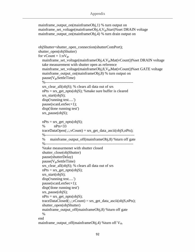
Appendix
92
mainframe_output_on(mainframeObj,1) % turn output on
mainframe_set_voltage(mainframeObj,4,VgsStart)%set DRAIN voltage
mainframe_output_on(mainframeObj,4) % turn drain output on
objShutter=shutter_open_connection(shutterComPort);
shutter_open(objShutter)
for vCount = 1:nVgs
mainframe_set_voltage(mainframeObj,4,VgsMat(vCount))%set DRAIN voltage
take measurement with shutter open as reference
mainframe_set_voltage(mainframeObj,8,VgsMat(vCount))%set GATE voltage
mainframe_output_on(mainframeObj,8) % turn output on
pause(VgsSettleTime)
%---------------------------------------------------------------------
srs_clear_all(objS); % clears all data out of srs
nPts = srs_get_npts(objS); %make sure buffer is cleared
srs_start(objS);
disp('running test.....')
pause(scanLenSec+1);
disp('done running test')
srs_pause(objS);
nPts = srs_get_npts(objS);
% nPts=33
traceDataOpen(:,:,vCount) = srs_get_data_ascii(objS,nPts);
%----------------------------------------------------------------------
% mainframe_output_off(mainframeObj,8) %turn off gate
%---------------------------------------------------------------------
%take measurmenet with shutter closed
shutter_close(objShutter)
pause(shutterDelay)
pause(VgsSettleTime)
srs_clear_all(objS); % clears all data out of srs
nPts = srs_get_npts(objS);
srs_start(objS);
disp('running test.....')
pause(scanLenSec+1);
disp('done running test')
srs_pause(objS);
nPts = srs_get_npts(objS);
traceDataClosed(:,:,vCount) = srs_get_data_ascii(objS,nPts);
shutter_open(objShutter)
mainframe_output_off(mainframeObj,8) %turn off gate
%
end
mainframe_output_off(mainframeObj,4) %turn off Vds
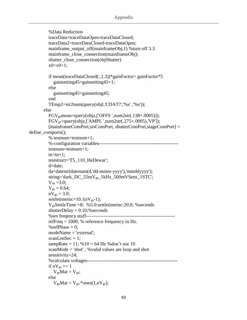
Appendix
93
%Data Reduction
traceData=traceDataOpen-traceDataClosed;
traceData2=traceDataClosed-traceDataOpen;
mainframe_output_off(mainframeObj,1) %turn off 3.3
mainframe_close_connection(mainframeObj);
shutter_close_connection(objShutter)
x0=x0+1;
if mean(traceDataClosed(:,1,3))*gainFactor> gainFactor*5
gainsetting45=gainsetting45+1;
else
gainsetting45=gainsetting45;
end
TEmp2=str2num(query(objl,'CDAT?','%s' ,'%s'));
else
FGVgsmean=query(objz,['OFFS ',num2str(.138+.0005)]);
FGVgs=query(objz,['AMPL ',num2str(.275+.0005),'VP']);
[mainframeComPort,srsComPort, shutterComPort,stageComPort] =
define_comports();
% testnum=testnum+1;
%-configuration variables-------------------------------------------------
testnum=testnum+1;
tn=tn+1;
teststruct='T5_110_HeDewar';
d=date;
da=datestr(datenum(d,'dd-mmm-yyyy'),'mmddyyyy');
string='dark_DC_55mVgs_1kHz_500mVSens_1STC';
Vds =3.0;
Vgs = 0.64;
nVgs = 3.0;
settletimeinc=10./(nVgs-1);
VgsSettleTime =8; %5.0:settletimeinc:20.0; %seconds
shutterDelay = 0.10;%seconds
%srs freqency stuff-------------------------------------------------------
refFreq = 1000; % reference frequency in Hz.
%refPhase = 0;
modeName = 'external';
scanLenSec = 1;
sampRate = 11; %10 = 64 Hz %don’t use 10
scanMode = 'shot' ; %valid values are loop and shot
sensitivity=24;
%calculate voltages--------------------------------------------------------
if nVgs == 1
VgsMat = Vgs;
else
VgsMat = Vgs.*ones(1,nVgs);

Appendix
94
end
%setup the SRS lockin ----------------------------------------------------
objS=srs_open(srsComPort);
srs_set_ref_freq(objS,refFreq); %Sets reference Frequency
%srs_set_ref_phase(objS,refPhase); %Sets reference Phase
srs_auto_phase(objS); % atuo phase at the start of each measurement
srs_set_ref_mode(objS,modeName) %Sets reference mode
srs_setup_traces(objS) %Sets up traces
sampRateVal=srs_set_sample_rate(objS,sampRate); %Sets sample rate-from fn.
srs_set_scan_mode(objS,scanMode); %Sets scan mode
srs_set_scan_len(objS,scanLenSec); %Sets scan time?
sensitivity=26;
%--------------------------------------------------------------------------
%Preamplifier gain setting
srsPre_open('COM7',gainsetting55)
gainFactor=CorrectGain(gainsetting55);
%channel #l 3.3, channel #4 = Vds, #8 Vgs-------------------------------------
% [mainframeObj] = mainframe_open_connection(mainframeComPort);
% mainframe_reset_powersupplies(mainframeObj); %reset power supplies
mainframe_set_voltage(mainframeObj,1,3.3)
mainframe_output_on(mainframeObj,1) % turn output on
mainframe_set_voltage(mainframeObj,4,Vds)%set DRAIN voltage
mainframe_output_on(mainframeObj,4) % turn drain output on
objShutter=shutter_open_connection(shutterComPort);
shutter_open(objShutter)
for vCount = 1:nVgs
%take measurmenet with shutter open as reference
% mainframe_set_voltage(mainframeObj,8,VgsMat(vCount))%set GATE voltage
% mainframe_output_on(mainframeObj,8) % turn output on
pause(VgsSettleTime)
%---------------------------------------------------------------------
srs_clear_all(objS); % clears all data out of srs
nPts = srs_get_npts(objS); %make sure buffer is cleared
srs_start(objS);
disp('running test.....')
pause(scanLenSec+1);
disp('done running test')
srs_pause(objS);

Appendix
95
nPts = srs_get_npts(objS);
% nPts=33
traceDataOpen(:,:,vCount) = srs_get_data_ascii(objS,nPts);
%----------------------------------------------------------------------
% mainframe_output_off(mainframeObj,8) %turn off gate
%---------------------------------------------------------------------
%take measurmenet with shutter closed
shutter_close(objShutter)
pause(shutterDelay)
% mainframe_set_voltage(mainframeObj,8,VgsMat(vCount))%set GATE voltage
% mainframe_output_on(mainframeObj,8) % turn output on
pause(VgsSettleTime)
srs_clear_all(objS); % clears all data out of srs
nPts = srs_get_npts(objS);
srs_start(objS);
disp('running test.....')
pause(scanLenSec+1);
disp('done running test')
srs_pause(objS);
nPts = srs_get_npts(objS);
traceDataClosed(:,:,vCount) = srs_get_data_ascii(objS,nPts);
% fprintf(shuttercon,'A'); %close shutter
shutter_open(objShutter)
% mainframe_output_off(mainframeObj,8) %turn off gate
%
end
mainframe_output_off(mainframeObj,4) %turn off Vds
%Data Reduction
traceData=traceDataOpen-traceDataClosed;
traceData2=traceDataClosed-traceDataOpen;
mainframe_output_off(mainframeObj,1) %turn off 3.3
% mainframe_close_connection(mainframeObj);
shutter_close_connection(objShutter)
x0=x0+1;
if mean(traceDataClosed(:,3,1))*gainFactor>gainFactor
gainsetting55=gainsetting55+1;
else
gainsetting55=gainsetting55;
end
TEmp2=str2num(query(objl,'CDAT?','%s' ,'%s'));
end
%% AC DATA FIGURES

Appendix
96
%Plots LI RMS measurements
str=sprintf('T5 110 %.0f GHz %0.5e AV Vds=%f',freq,gainFactor,Vds);
figure;
meanVolts = zeros(nVgs,3);
vcount=1:nVgs;
for vCount = 1:nVgs
curVgs(:) = (vCount);
plot(curVgs,traceDataOpen(:,3,vCount)*gainFactor,'*r')
hold on
plot(curVgs,traceDataClosed(:,3,vCount)*gainFactor,'*b')
hold on
plot(curVgs,traceData(:,3,vCount)*gainFactor,'*g')
meanVolts(vCount,1) = mean(traceDataOpen(:,3,vCount));
meanVolts(vCount,2) = mean(traceDataClosed(:,3,vCount));
meanVolts(vCount,3) = mean(traceDataOpen(:,3,vCount))-
mean(traceDataClosed(:,3,vCount));
end
plot(vcount,meanVolts(:,1)*gainFactor,'-r')
plot(vcount,meanVolts(:,2)*gainFactor,'-b')
plot(vcount,meanVolts(:,3)*gainFactor,'-g')
title(str)
xlabel('Test Number')
ylabel('Measured Ids (A)')
%
filenamefigs=sprintf('C:\\Users\\A270-
THz\\Dropbox\\kennys_thz_matlab\\Tests\\%s\\%s\\figures\\Test%d__AC%.0fGHz_gain%.0d_
%s_%d',da,teststruct,testnum,freq,gainFactor,string,round(TEmp,0));
savefig(filenamefigs)
%% DC DATA FIGURES
%Plots A/D data
str=sprintf('T5 110 %.0f GHz %0.5e AV Vds=%f',freq,gainFactor,Vds);
figure
meanVolts = zeros(nVgs,3);
vcount=1:nVgs;
for vCount = 1:nVgs
curVgs(:) = (vCount);
plot(curVgs,traceDataOpen(:,1,vCount)*gainFactor,'*r')
hold on
plot(curVgs,traceDataClosed(:,1,vCount)*gainFactor,'*b')
hold on
% plot(curVgs,traceData(:,1,vCount)*gainFactor,'*g')
meanVolts(vCount,1) = mean(traceDataOpen(:,1,vCount));

Appendix
97
meanVolts(vCount,2) = mean(traceDataClosed(:,1,vCount));
meanVolts(vCount,3) = mean(traceDataOpen(:,1,vCount))-
mean(traceDataClosed(:,1,vCount));
end
plot(vcount,meanVolts(:,1)*gainFactor,'.r')
plot(vcount,meanVolts(:,2)*gainFactor,'.b')
plot(vcount,meanVolts(:,3)*gainFactor,'.g')
title(str)
xlabel('Test Number')
ylabel('Ids')
filenamefigs=sprintf('C:\\Users\\A270-
THz\\Dropbox\\kennys_thz_matlab\\Tests\\%s\\%s\\figures\\Test%d__DC%.0fGHz_gain%.0d_
%s_%d',da,teststruct,testnum,freq,gainFactor,string,round(TEmp,0));
savefig(filenamefigs)
%% Saves Matlab Workshop
filename=sprintf('C:\\Users\\A270-
THz\\Dropbox\\kennys_thz_matlab\\Tests\\%s\\%s\\Test%d_%.0fGHz_gain%.0d_%s_%d',da,tes
tstruct,testnum,freq,gainFactor,string,round(TEmp,0));
save(filename)
else
disp('not yet')
end
else
disp('not yet')
end
pause(30)
end

98
References
[1] A. Rogalski. F. Sizov, "Terahertz detectors and focal plane arrays," Opto-Electronics Review, vol.
19, no. 3, pp. 346-404, 2011. Springer. DOI: 10.2478/s11772−011−0033−3
[2] T. M., "Cutting-edge terahertz technology," nature photonics, vol. 01, pp. 97-105, February 2007.
www.nature.com/naturephotonics
[3] E. Brundermann. et al., Terahertz Techniques, Springer Series in Optical Sciences, Berlin
Heidelberg: Springer-Verlag, 2012. DOI: 10.1007/978-3-642-02592
[4] G. Fertig, "Evaluation of MOSFETs for Terahertz Detector Arrays," 15 August, 2014. Rochester
Institute of Technology
[5] C. M. Armstrong, The truth about terahertz, IEEE Spectrum, 2012.
[6] M. Perenzoni and D. J. Paul, Eds., Physics and Applications of Terahertz Radiation, vol. Springer
Series in Optical Sciences 173, Springer Science+Business Media Dordrecht, 2014.
[7] R. Appleby and J. M. Chamberlain, "Terahertz Frequency Security Systems and Terahertz Safety
Considerations," in Physics and Applications of Terahertz Radiation, vol. Springer Series in Optical
Sciences 173, M. Perenzoni and D. J. Paul, Eds., Springer, 2014, pp. 233-255. DOI: 10.1007/978-
94-007-3837-9_2
[8] M. Saviz, O. Spathmann, J. Streckert, V. Hansen, M. Clemens and R. Faraji-Dana, "Theoretical
Estimations of Safety Thresholds for Terahertz Exposure of Surface Tissues," IEEE Transactions
on Terahertz Science and Technology, vol. 3, no. 5, pp. 635-640, September 2013. DOI:
10.1109/TTHZ.2013.2264327
[9] P. H. Siegel, "Terahertz Technology," IEEE TRANSACTIONS ON MICROWAVE THEORY AND
TECHNIQUES, vol. 50, no. 3, pp. 910-927, March 2002. PII: 0018-9480(02)01958-0
[10] D. J. Newman, et al., "Compact THz Imaging Detector," in SPIE DSS 2013, 2013.
[11] K. Su, "Terahertz Wireless Communication," New Jersey Institute of Technology and Rutgers,
January 2012.
[12] J. Sun, Field-effect Self-mixing Terahertz Detectors, Springer, 2016. DOI: 10.1007/978-3-662-
48681-8
[13] D. J. Benford, J. G. Staguhn, G. J. Stacey, L. A. Page, S. H. Moseley, K. D. Irwin, J. A. Chervenak
and C. A. Allen, "Design and Fabrication of Two-Dimensional Superconducting Bolometer
Arrays," Millimeter and Submillimeter Detectors for Astronomy II, vol. 5498, pp. 647-658, 2004.
[14] A. Pletersek and J. Trontelj, "A Self-Mixing NMOS Channel-Detector Optimized," J Infrared Milli
Terahz Waves, vol. 33, pp. 615-626, 2012. DOI: 10.1007/s10762-012-9901-2

References
99
[15] Y. Huo, "A TERAHERTZ RADIATION DETECTION SYSTEM DESIGN AND," University of
Connecticut, 2003. UMI: 3078042 fix
[16] F. F. Sizov, V. P. Reva, A. G. Golenkov and V. V. Zabudsky, "Uncooled Detectors Challenges for
THz/sub-THz," J Infrared Milli Terahz Waves, vol. 32, pp. 1192-1206, 2011. Springer
Science+Business Media. DOI: 10.1007/s10762-011-9789-2
[17] J. F. Federici, B. Shulkin, F. Huang, D. Gary, R. Barat, F. Oliveira and D. Zimdars, "THz imaging
and sensing for security," Semicond. Sci. Technol., vol. 20, pp. 266-280, 2005.
[18] P. H. Siegel, "Terahertz Technology in Biology and Medicine," IEEE MIT-S Digest, pp. 1575-1578,
2004.
[19] TeraView Limited, "Using the TPS Spectra 3000 as a Tool for the Investigation of Cancers: Using
the Hand-held Probe to Investigate Breast Cancer," [Online]. Application note, Available:
http://www.teraview.com.
[20] S. Suzuki, T. Nukariya, Y. Ueda, T. Otsuka and M. Asada, "High Current Responsivity and Wide
Modulation," J Infrared Milli Terahz Waves, vol. 37, pp. 658-667, 2016. Springer. DOI:
10.1007/s10762-016-0260-2
[21] K. Yasuko, "7 Terahertz-Wave Remote Sensing," Journal of the National Institute of Information
and Communications Technology, vol. 55, no. 1, 2008. URL:
http://www.nict.go.jp/publication/shuppan/kihou-journal/journal-vol55no1/07-01.pdf
[22] Suen J.Y, Fang M.T., Lubin P.M. “Global Distribution of Water Vapor and Cloud Cover—Sites for
High Performance THz Applications” http://www.deepspace.ucsb.edu/projects/b-machine 2014
[23] K. Peiponen, J. A. Zeitler and M. Kuwata-Gonokami, Eds., Terahertz Spectroscopy and Imaging,
vol. 171, Springer, 2013. DOI: 10.1007/978-3-642-29564-5
[24] A. P. Sacco, J. D. Newman, P. P. K. Lee, K. D. Fourspring and e. a. John H. Osborn, "THz imaging
Si MOSFET system design at 215 GHz," in Terahertz Physics, Devices, and Systems VIII, May 21,
2014. DOI: 10.1117/12.2050906. URL: http://dx.doi.org/10.1117/12.2050906
[25] CEIS, "Center for emerging and innovative sciences.," [Online]. Available:
http://www.ceis.rochester.edu/about/index.html. [Accessed 2017].
[26] S. M. Sze and K. N. Kwok, Physics of Semiconductor Devices, Third ed., New Jersey: John Wiley
& Sons, Inc, 2007.
[27] B. G. Streetman and S. K. Banerjee, Solid State Electronic Devices, Sixth ed., Prentice-Hall, 2006.
[28] D. Kahng, "A Historical Perspective on the Development of MOS Transistors and Related
Devices," IEEE Transactions on Electron Devices, vol. 7, pp. 655-657, 07 July 1976.
[29] P. Horowitz and W. Hill, Art of Electronics, Second ed., Cambridge University Press, 1989.

References
100
[30] A. Wang, B. H. Calhoun and A. P. Chandrakasan, Sub-threshold Design for Ultra Low-Power
Systems, Springer, 2006, p. 209. URL: http://www.springer.com/978-0-387-33515-5
[31] A. Tajalli and Y. Leblebici, Extreme Low-Power Mixed Signal IC Design, Springer, 2010, pp. pp
15-58. DOI: 10.1007/978-1-4419-6478-6_2
[32] M. Sakhno, F. Sizov and A. Golenkov, "Uncooled THz/sub-THz Rectifying Detectors," J Infrared
Milli Terahz Waves, pp. 798-814, 2013. DOI: 10.1007/s10762-013-0023-2
[33] J. Ma, "Hot Carrier Study of MOSFET at 300K and 77K," Stony Brook University, December 2015.
ProQuest: 10017965
[34] D. Wolpert and P. Ampadu, Managing Temperature Effects in Nanoscale Adaptive Systems,
Springer, 2012, p. 174. URL: http://www.springer.com/978-1-4614-0747-8
[35] M. Dyakonov and M. Shur, "Shallow Water Analogy for a Ballistic Field Effect Transistor: New
Mechanism of Plasma Wave Generation by dc Current," Physical Review Letters, vol. 71, no. 15,
11 October 1993.
[36] M. Dyakonov and M. S. Shur, "Plasma Wave electronics: Novel Terahertz Devices using Two
Dimensional Electron Fluid," IEEE Transactions on Electron Devices, vol. 43, no. 10, October
1996.
[37] T. A. Elkhatib, "Terahertz Response of Field-Effect Transistors in Saturation Regime," Rensselaer
Polytechnic Institute, April 2010. UMI: 3420916
[38] W. J. Stillman, "Silicon CMOS FETs as Terahertz and Sub-Terahertz Detectors," Rensselaer
Polytechnic Institute, 2008. UMI: 3329048
[39] D. B. Veksler, "Plasma Wave Electronics Devices for THz Detection," Rensselaer Polytechnic
Institute, August 2007. UMI: 3286347
[40] A. Gutin, "Terahertz Plasmonic Field Effect Transistor," Rensselaer Polytechnic Institute,
November 2012. UMI: 3571044
[41] D. M. Yermolayev, E. A. Polushkin, S. Shapoval, V. V. Popov, K. V. Marem'yanin, V. I.
Davrilenko, V. M. Ustinov and e. al, "Detection of Terahertz Radiation by Dense Arrays of InGaAs
Transistors," International Journal of High Speed Electronics and Systems, vol. 24, no. 1&2, 2015.
DOI: 10.1142/S0129156415500020
[42] J. B. Dayalu, et al., "Terahertz Detection in Si MOSFET based on Thermionic Emission," in IEEE
International Conference on Microwaves, Communications, Antennas and Electronic Systems, Tel
Aviv, 2015.
[43] F. Schuster, D. Coquillat, H. Videlier, M. Sakowicz, F. Teppe, L. Dussopt, B. Giffard, T. Skotnicki
and W. Knap, "Broadband terahertz imaging with highly sensitive silicon CMOS detectors,"
OPTICS EXPRESS, vol. 19, no. 8, 07 April 2011.
References
101
[44] P. Kopyt, B. Salski, J. Marczewski, P. Zagrajek and J. Luskowski, "Parasitic Effects Affecting
Responsivity of Sub-THz Radiation Detector Built of a MOSFET," J Infrared Milli Terahz Waves,
vol. 36, pp. 1059-1075, 2015. DOI: 10.1007/s10762-015-0188-y
[45] C. Zhang, "Optical Simulation of terahertz antenna using finite difference time domian method,"
Rochester Institute of Technology. 2015.
[46] Stanford Research Systems, "SR850 Manual". 2015 URL:
http://www.thinksrs.com/products/SR850.htm
[47] A. Ortiz-Conde, F. G. Sanchez, J. J. Liou, A. Cerderia, M. Estrada and Y. Yue, "A review of recent
MOSFET threshold voltage," Microelectronics Reliability, vol. 42, pp. 583-596, 2002. Elsevier
Science Ltd. PII: S0026-2714(02)00027- 6. URL: www.elsevier.com/locate/microrel
[48] S. M. Sharroush, Y. S. Abdalla, A. A. Dessouki and E. A. El-Badawy, "Subthreshold MOSFET
Transistor Amplifier Operation," November 2009. URL:
https://www.researchgate.net/publication/261095502 [Date Accessed: 21 November, 2016].
DOI: 10.1109/IDT.2009.5404144
[49] P. Foldesy, "Characterization of silicon field effect transistor sub-THz detectors for imaging
systems," May 2012. URL: https://www.researchgate.net/publication/236888504. DOI:
10.1109/ISCAS.2012.6272198
[50] P. Mayer, "Current Fluctuations in Semiconductor Devices," Department of Electrical Engineering
and Computer Science, 2002. Massachusetts Institute of Technology.
[51] C. Jakobson, I. Bloom and Y. Nemirovsky, "1/F NOISE IN CMOS TRANSISTORS FOR
ANALOG APPLICATIONS FROM SUBTHRESHOLD TO SATURATION," Solid-State
Electronics, vol. 42, no. 10, pp. 1807-1817, 1998. DOI: S0038-1101(98)00162-2
[52] D. B. But, et al., "Silicon Field-Effect Transistors as Radiation Detectors for the Sub-THz Range,"
Fizika i Tekhnika Poluprovodnikov, vol. 46, no. 5, pp. 695-700, 2012. Pleiades Publishing, Ltd.
DOI: 10.1134/S1063782612050107
[53] M. Sakowicz, et al., "Terahertz responsivity of field effect transistors versus their static channel
conductivity and loading effects," Journal of Applied Physics, vol. 110, 2011. DOI:
10.1063/1.3632058
[54] M. Azlishah bin Othman, "Sub-Terahertz: Generation and Detection," The University of
Nottingham, June 2013.
[55] J. F. Allnutt, Testing and Characterization of Silicon Devices at Cryogenic Temperatures,
University of Maryland, College Park, 2007.
[56] C. Corsi, F. Sizov, "THz And Security Applications: Detectors, Sources, and Associated Electronics
for THz Applications," in NATO Advanced Research Workshop on THz and Security Applications-
Detectors, Sources and Associated Electronics for THz Applications, Kiev, 2013.
[57] D. B. But, C. N. Dyakonova, F. Teppe, S. Ruffenach, W. Knap, P. Kopyt and J. Marczewski,
"Substrate Optimization for a planar antenna of terahertz Si field effect transistor detectors," 2016
References
102
21st International Conference on Microwave, Radar, and Wireless Communications (MIKON),
2016.
[58] D. Coquillat, J. Marczewski, P. Kopyt, N. Dyakonova, B. Giffard and W. Knap, "Improvement of
terahertz field effect transistor detectors by substrate thinning and radiation losses reduction,"
Optics Express 272, vol. 24, no. 1, 2016.
[59] Stanford Research Systems, "SR570 Low Noise Current Preamplifier," 2015. URL:
http://www.thinksrs.com/products/SR570.htm
[60] J. Weibler, "Properties of Metals Used for RF Shielding," EMC Test & Design, December 1993.
Lindgren RF Enclosures, Inc.
[61] Klimenko, O., Knap, W., Iniguez, B., Coquillat, D., & Mityagin, e. (2012). Temperature
enhancement of terahertz responsivity of plasma field effect transistors. Journal of Applied Physics,
112(014506), 1-5. doi:10.1063/1.4733465
[62] Kawase, K., Ogawa, Y., Watanabe, Y., & Inoue, H. (2003). Non-destructive terahertz imaging of
illicit drugs using spectral fingerprints. Optics Express 2549-2554, vol 11 no. 20, Optical Society of
America
[63] TeraView Limited, "Using the TPS Spectra 3000 as a Tool for the Investigation of Cancers:
Terahertz Spectroscopy of Human Breast Cancer," [Online]. Application note, Available:
http://www.teraview.com.
[64] Mao Q., et al. “Effective receiving area of the antenna-coupled terahertz detector,” Optical
Engineering. Vol 53 no.2. SPIE. February 2014
[65] Kohin M., Butler N. “Performance Limits of Uncooled VOx Microbolometer Focal Plane Arrays,”
Infrared Technology and Applications XXX, Proc. Of SPIE Vol. 5406 DOI: 10.1117/12.542482
[66] NEC, Terahertz Imager, Website: http://www.nec.com/en/global/prod/terahertz/index.html