Characterization of Magnetic Nanostructures Using … · ARIZONA STATE UNIVERSITY ... This...
146
Characterization of Magnetic Nanostructures Using Off-Axis Electron Holography by Desai Zhang A Dissertation Presented in Partial Fulfillment of the Requirements for the Degree Doctor of Philosophy Approved April 2015 by Graduate Supervisory Committee: Martha R. McCartney, Co-Chair David J. Smith, Co-Chair Peter A. Crozier Ralph V. Chamberlin William T. Petuskey ARIZONA STATE UNIVERSITY May 2015
Transcript of Characterization of Magnetic Nanostructures Using … · ARIZONA STATE UNIVERSITY ... This...

Characterization of Magnetic Nanostructures
Using Off-Axis Electron Holography
by
Desai Zhang
A Dissertation Presented in Partial Fulfillment
of the Requirements for the Degree
Doctor of Philosophy
Approved April 2015 by
Graduate Supervisory Committee:
Martha R. McCartney, Co-Chair
David J. Smith, Co-Chair
Peter A. Crozier
Ralph V. Chamberlin
William T. Petuskey
ARIZONA STATE UNIVERSITY
May 2015

i
ABSTRACT
This dissertation research has involved microscopic characterization of magnetic
nanostructures using off-axis electron holography and Lorentz microscopy. The
nanostructures investigated have included Co nanoparticles (NPs), Au/Fe/GaAs shell/core
nanowires (NWs), carbon spirals with magnetic cores, magnetic nanopillars, Ni-Zn-Co
spinel ferrite and CoFe/Pd multilayers. The studies have confirmed the capability of
holography to describe the behavior of magnetic structures at the nanoscale.
The phase changes caused by the fringing fields of chains consisting of Co NPs were
measured and calculated. The difference between chains with different numbers of Co NPs
followed the trend indicated by calculations. Holography studies of Au/Fe/GaAs NWs
grown on (110) GaAs substrates with rotationally non-uniform coating confirmed that Fe
was present in the shell and that the shell behaved as a bar magnet. No fringing field was
observed from NWs with cylindrical coating grown on (111)B GaAs substrates. The most
likely explanation is that magnetic fields are confined within the shells and form closed
loops. The multiple-magnetic-domain structure of iron carbide cores in carbon spirals was
imaged using phase maps of the fringing fields. The strength and range of this fringing
field was insufficient for manipulating the carbon spirals with an external applied magnetic
field. No magnetism was revealed for CoPd/Fe/CoPd magnetic nanopillars. Degaussing
and MFM scans ruled out the possibility that saturated magnetization and sample
preparation had degraded the anisotropy, and the magnetism, respectively. The results
suggested that these nanopillars were not suitable as candidates for prototypical bit
information storage devices.

ii
Observations of Ni-Zn-Co spinel ferrite thin films in plan-view geometry indicated a
multigrain magnetic domain structure and the magnetic fields were oriented in-plane only
with no preferred magnetization distribution. This domain structure helps explain this
ferrite’s high permeability at high resonance frequency, which is an unusual character.
Perpendicular magnetic anisotropy (PMA) of CoFe/Pd multilayers was revealed
using holography. Detailed microscopic characterization showed structural factors such as
layer waviness and interdiffusion that could contribute to degradation of the PMA.
However, these factors are overwhelmed by the dominant effect of the CoFe layer
thickness, and can be ignored when considering magnetic domain structure.

iii
This dissertation is dedicated to
my cat, Athena.
I did,
like Don Quixote challenging the windmill.
iv
ACKNOWLEDGMENTS
I would like to express my deepest appreciation to my mentors Professor Martha R.
McCartney and Regents’ Professor David J. Smith for their guidance and training that
helped me achieving toward my degree. What I learned from them is not only knowledge
and experience, but also the positive attitude and determination in solving the tasks that
sent to test me. I would also like to thank my supervisory committees, Professors Peter A.
Crozier, Ralph V. Chamberlin and William T. Petuskey, for their time and suggestions.
I would like to acknowledge the stuff members as well as the use of facilities in John
M. Cowley Center for High Resolution Electron Microscopy at Arizona State University.
Special thanks to Mr. Karl Weiss and Dr. Toshihiro Aoki for their technical assistance.
Most of the works in this dissertation were supported by US Department of Energy (Grant
DE-FG02-04ER46168). Financial supports without any expectation of return from my
parents, Mr. Zhang and Mrs. Pan, are also gratefully acknowledged.
I appreciate collaborations with Dr. N. Ray (Arizona State University), Prof. J. K.
Furdyna (University of Notre Dame), Dr. J. Shaw (NIST), Prof. J. Pyun (University of
Arizona), Prof. C-L. Chien (John Hopkins University), Prof. F. Hellman (University of
California, Berkeley), Prof. E. Fullerton (University of California, San Diego), Dr. H.
Shiozawa (University of Vienna), Dr. S. Parkin (IBM Almaden Research Center), Prof. C.
Felser (Max-Planck Institut) and Prof. A. Demkov (University of Texas at Austin), who
provided the samples. I also thank Prof. T. Chen (Arizona State University) and Prof. L.
Gu (Institute of Physics, Chinese Academy of Science) for use of their facilities.

v
Particular thanks to my colleagues in ‘MDG’ who generously share their knowledge
and expertise with me.

vi
TABLE OF CONTENTS
Page
LIST OF FIGURES .............................................................................................................x
LIST OF TABLE ............................................................................................................. xix
CHAPTER
1 INTRODUCTION ............................................................................................................1
1.1. Background .................................................................................................................. 1
1.2. Principles of Magnetism .............................................................................................. 2
1.3 Characterization of Magnetic Material ......................................................................... 8
1.3.1 Bulk Methods ..................................................................................................... 8
1.3.2 Microscopic Methods ......................................................................................... 9
1.3.3 TEM Based Methods ........................................................................................ 10
1.4 Examination and Applications of Magnetic Nanostructures ...................................... 12
1.4.1 Magnetic Nanoparticles .................................................................................... 12
1.4.2 Magnetic Nanowires and Nanorods. ................................................................ 13
1.4.3 Magnetic Structures for Spin Electronics ......................................................... 16
1.4.4 Patterned Magnetic Nanostructures .................................................................. 17
1.5 Outline of Dissertation ................................................................................................ 19
References ......................................................................................................................... 21
2 EXPERIMENTAL DETAILS AND METHODS ..........................................................24

vii
CHAPTER Page
2.1 Material Growth and Sample Preparation................................................................... 24
2.1.1 Magnetron Sputtering Deposition .................................................................... 24
2.1.2 Molecular Beam Epitaxy .................................................................................. 25
2.2 TEM Sample Preparation ............................................................................................ 26
2.3 Instrumentation ........................................................................................................... 27
2.4 Electron Holography ................................................................................................... 29
2.4.1 Experimental Settings ....................................................................................... 29
2.4.2 Processing of Phase Maps ................................................................................ 35
References ......................................................................................................................... 40
3 EXAMINATION OF MAGNETIC NANOSTRUCTURES ..........................................41
3.1 Co Nanoparticles ......................................................................................................... 41
3.2 Core/Shell Magnetic Nanowires ............................................................................... 47
3.3. Carbon Spirals from Symmetric Iron Carbide Magnetic Core .................................. 59
3.4 Magnetic Nanopillars .................................................................................................. 62
References ......................................................................................................................... 73
4 CHARACTERIZATION OF DOMAIN STRUCTURE IN THIN FILM OF
NANOCRYSTALLINE Ni-Zn-Co SPINEL FERRITE ....................................................75
4.1 Introduction ................................................................................................................. 75
4.2 Experimental Details ................................................................................................... 77

viii
CHAPTER Page
4.3 Results and Discussion ............................................................................................... 78
4.3.1 Sample Permeability ......................................................................................... 78
4.3.2 Crystal Structure ............................................................................................... 79
4.3.3. Chemical Composition. ................................................................................... 81
4.3.4. Magnetic Domain Structure............................................................................. 82
4.4 Conclusions ................................................................................................................. 89
References ......................................................................................................................... 91
5 PERPENDICULAR MAGNETIC ANISOTROPY AND MAGNETIC DOMAINS IN
CoFe/Pd MULTILAYERS ................................................................................................93
5.1 Introduction ................................................................................................................. 93
5.2 Experimental Details ................................................................................................... 94
5.3 Results and Discussion ............................................................................................... 96
5.3.1 Surface Morphology ......................................................................................... 96
5.3.2 Crystalline Structure ......................................................................................... 98
5.3.3 Magnetic Domain Structure............................................................................ 101
5.4 Conclusions ............................................................................................................... 106
References ....................................................................................................................... 108
6 SUMMARY AND POSSIBLE FUTURE WORK .......................................................110
6.1 Summary ................................................................................................................... 110

ix
CHAPTER Page
6.2 Future Work: Skyrmions........................................................................................... 112
6.2.1 Introduction .................................................................................................... 112
6.2.2 Target Material ............................................................................................... 113
6.2.3 Revealing Skyrmions using Off-axis Electron Holography ........................... 114
References ....................................................................................................................... 117
References ........................................................................................................................119

x
LIST OF FIGURES
Figure Page
1. 1. Hysteresis Loop of a Ferromagnetic Material, Where Ms is Saturated Magnetization,
Mr is Remnant Magnetization and Hc is Coercivity Field. ........................................ 3
1. 2. Magnetization Distributions of (a) Classic U-Shaped Magnet, and (b) U-Shaped
Magnetic Nanostructure. ............................................................................................ 5
1. 3. Illustration of the Crystallographic Alignments of the Magnetic Moments in Iron
which is a Body-Centered-Cubic Material, and Nickel, which is Face-Centered-Cubic.
.................................................................................................................................... 5
1. 4. Schematic of Domain Wall Structures for: (a) Bloch Wall, and (b) Néel Wall.4 ....... 7
1. 5. Schematic of Ray Diagram Indicating the Paths Followed by Electrons Passing
through a Magnetic Specimen with Domain Walls, Together with the Contrast that
would be Visible in the Image using the Fresnel and Foucault Modes of Lorentz
TEM.22 ..................................................................................................................... 11
1. 6. Phase Contours Showing the Strength of the Local Magnetic Induction in Two
Different Chains of Fe0.56Ni0.44 Particles, Recorded using Off-axis Electron
Holography, Indicating Vortex in: (a) Single Particle, and (b) Ring of Particles.24-25
.................................................................................................................................. 12
1. 7. (a) Hologram (Acquired at 120 keV) and (b) Associated Remnant B Map of A
Cu/CoFeB (50/50 nm) NW for a Magnetic Field Applied Parallel to the Axis of the
NW prior to the Hologram Acquisition. 31 ............................................................... 14

xi
Figure Page
1. 8. Schematic of Racetrack Memory using Ferromagnetic Nanowire in (a) Vertical
Configuration and (b) Horizontal Configuration. Data Encoded as a Pattern of
Magnetic Domains Along a Portion of the Wire. Pulses of Highly Spin-Polarized
Current Move the Entire Pattern of Domain Walls Coherently along the Length of
the Wire Past Read-and-Write Elements.32 .............................................................. 15
1. 9. (a) Synthesis Procedure for Nanorods with Cobalt (Cobalt Oxide) Nanoparticle ‘Tip’
with Platinum Core; (b) and (c) TEM Images of Low and High Magnification
Showing Network Consisting of Nanorods.33 .......................................................... 16
1. 10. (a) Band Structure of Spintronic Diode. (b) Schematic of Spintronic MOSFET.35 17
1. 11. Magnetic Induction Maps for C-Shaped Cobalt Nanostructure Obtained using
Electron Holography.36 ............................................................................................ 18
1. 12. Schematic Illustration of Method Used to Fabricate Magnetic Nanopillars.40 ....... 19
2. 1. Schematic of Planar Magnetron Sputtering System.3 ……………………………25
2. 2. Schematic of Procedure Used for Preparing Cross-Section TEM Samples. ............ 27
2. 3. Microscopes Used for the Majority of the Research Described in this Dissertation.
.................................................................................................................................. 29
2. 4. (a) Schematic Showing the Essential TEM Components for Off-axis Electron
Holography, (b) Photo of CM-200 Showing Locations of Key Components. ........ 30
2. 5. Schematic Illustration of the Origin of the Phase Shifts Studied by Off-axis Electron
Holography.12 ........................................................................................................... 32

xii
Figure Page
2. 6. (a) Schematic Diagram Showing the Use of Specimen Tilt to Provide the In-plane
Component of the Applied Field Needed for In Situ Magnetization Reversal
Experiments; (b) and (c) Hall Probe Measurement of Magnetic Field in the Specimen
Plane of Philips CM200 and TITAN as a Function of Objective Lens Current.10 .. 34
2. 7. Image Reconstruction for Extracting Phase and Amplitude Information from
Hologram of AlFeNiCo Alloy. ................................................................................ 37
2. 8. (a) Reconstructed Phase Image in Pseudo-Color Mode Showing Relative Phase
Change; (b) and (c) Gradient of Phase, Directions of Derivatives are Marked by Black
Arrows 1 and 2 in (a); (d) Phase Gradient Vectors Map; (e) Magnetic Induction Map
Using RGB Color Encoding the Directions; (f) Color Wheel Indicating Relation
between Colors and Directions of the Magnetic Induction. .................................... 39
3. 1. Bright-Field TEM Images of Co Nps at: (a) Low; and (b) High Magnification.
……………………………………………………………………………………42
3. 2. (a) Selected-area Electron Diffraction Pattern From Co Nanoparticles; (b) High-
Resolution Phase Contrast Image of a Single Co NP Used for Lattice-spacing
Measurement. ........................................................................................................... 43
3. 3. Original Hologram of a Chain of Seven Co Particles. .............................................. 44
3. 4. (a) and (b) Phase Maps Generated Using Opposite Tilting Technique; (c) and (d)
Corresponding Line Profiles from the Positions Indicated by Square Boxes in (a) and
(b), Respectively. ..................................................................................................... 45
3. 5. SEM Images of GaAs/Fe/Au Core/Shell NWs Grown on ZB GaAs: (a) (111)B, and
(b) (110), Respectively............................................................................................. 48

xiii
Figure Page
3. 6. Angular Dependence of the Resonance Field (Hres) of GaAs/Fe/Au Core/Shell NWs
Grown on (110) Substrate.16 .................................................................................... 50
3. 7. SANS Data of Nws Grown on (111)B Substrate: Sum of the Spin-Flip Scattering (+-
And -+).16 ................................................................................................................ 50
3. 8. TEM Images of GaAs/Fe/Au Core/Shell NWs Grown on: (a) (111)B and (b) (110) ZB
GaAs, Respectively. ................................................................................................. 52
3. 9. High-resolution TEM Images of GaAs/Fe/Au Core/Shell NWs: (a) GaAs Core
Showing Highly Defective WZ Structure. (b) Shell Region with Au 2.35 Å Lattice
Fringes Visible. ........................................................................................................ 52
3. 10. Bright Field Cross-section TEM Image of GaAs/Fe/Au Core/Shell Sample Including
NWs, Buffer Layer, and Substrate. .......................................................................... 53
3. 11. High-resolution Cross-section TEM Image near the Bottom Part of a GaAs/Fe/Au
Core/Shell NW. ........................................................................................................ 53
3. 12. Cross-section TEM Image Showing Highly Defective Top Surface of Buffer Layer
with ZB GaAs Phase. Lattice Direction in Each Grain Indicated by Arrows.......... 54
3. 13 EDXS Line Profile. Scan Position and Direction as Indicated in the Insert HAADF
Image. Overlap of Fe and O Signals Indicates Presence of Iron Oxide. ................. 55
3. 14 EELS Spectrum Taken on Shell of GaAs/Fe/Au Core/Shell NW Showing Oxygen K-
Edge and Iron L-Edge. ............................................................................................. 55
3. 15. Phase Maps of Au/Fe/GaAs Shell/Core Nanowires Grown on (a) (111)B and (b)
(110) ZB GaAs. The Directions of Magnetic Field Used to Magnetize the Sample are
Indicated. .................................................................................................................. 56
xiv
Figure Page
3. 16 Phase Map of GaAs/Fe/Au Core/Shell NW after Eliminating Phase Contribution from
Mean Inner Potential (Left), Line Profiles from Positions Marked by Arrows in Phase
Map (Right). ............................................................................................................. 58
3. 17. (a) Lorentz Image Showing the Line Profile Position; (b), (c) and (d) Line Profiles
from Reconstructed Phase Images Taken at Different Temperatures. .................... 59
3. 18. SEM Images of Carbon Spirals of Different Sizes. Bright Contrast at Center of Each
Spiral Correspond to Fe-rich Catalyst Particle.27 ..................................................... 60
3. 19. (a) TEM Image of Carbon Spirals formed from Iron Carbide Core; (b) and (c) SAED
from the Areas Marked in (a)................................................................................... 61
3. 20. (a) Lorentz Image of Carbon Spirals; (b), (c), (d) and (e) Phase Maps Generated on
Different Locations Marked in (a); (f) Schematic of Magnetic Field Lines that can
Possibly Cause the Phase Distribution in (d). .......................................................... 62
3. 21. Schematic Illustration of Processing Two Sets of Nanopillars. .............................. 64
3. 22. Plan-view TEM Images of (a) ‘Ref’ and (b) ‘80deg’ Nanopillars.......................... 64
3. 23. Cross-section TEM Image of ‘Ref’ Nanopillars in (a) Low and (c) High
Magnification; Cross-section TEM Image of ‘80deg’ Nanopillars in (b) Low and (d)
High Magnification. ................................................................................................. 65
3. 24. Schematic of Directions of Magnetic Field for In Situ Magnetizing. ..................... 66
3. 25. Phase Maps of ‘Ref’ Nanopillars in: (a) Cross-section, and (b) Plan-view Geometry.
.................................................................................................................................. 66
3. 26. Phase Maps of ‘80deg’ Nanopillars in: (a) Cross-section, and (b) Plan-view
Geometry.................................................................................................................. 67

xv
Figure Page
3. 27. Phase Maps after Degaussing Operation: (a) 'Ref' Sample in Cross-section Geometry,
(b) '80deg' Sample in Cross-section Geometry, (c) '80deg' Sample in Plan-view
Geometry.................................................................................................................. 68
3. 28. (a) MFM Scan, and (b) AFM Scan of 'Ref' Sample................................................ 69
3. 29. (a) MFM Scan, and (b) AFM Scan of '80deg' Sample............................................ 70
3. 30. ‘Out of Plane’ Hysteresis Loops Measured on ‘80deg’ Sample by VSM. ............. 71
3. 31. Lorentz Image of ’80deg’ Sample Taken with Sample Tilted and Objective Lens
Turned On. ............................................................................................................... 71
3. 32. Phase Map of ’80deg’ Sample Taken with Sample Tilted and Objective Lens Turned
On. ............................................................................................................................ 72
4. 1. Complex Permeability Spectrum of Ni0.24Zn0.61Co0.02Fe2.13O4 Spin-spray Ferrite Thin
Film. Solid Line Represents Real Part of Permeability ’ and Dash Line Represents
Imaginary Permeability
’’……………………………………………...…………………………………...79
4. 2. Low-magnification (a), and High-magnification (b), Bright-field TEM Images
Showing Cross-sections of Spin-spray Ferrite Film Deposited on Glass Substrate. 80
4. 3. Plan-view Bright-field TEM Image Showing Spin-spray Ferrite Deposited on Silicon
Substrate. Arrows Indicate Possible Porosity within the Film. ............................... 81
4. 4. Plan-view Bright-field TEM Image Showing Spin-spray Ferrite Deposited on Silicon
Substrate. Arrows Indicate Possible Porosity within the Film. ............................... 82

xvi
Figure Page
4. 5. (a) Plan-view Image Recorded Using Lorentz Mini-lens. (b) Reconstructed Phase Map
in Plan-view Obtained by Subtracting Two Electron Holograms to Eliminate
Contribution from Mean Inner Potential. (c) Magnetic Domain Map. Inserted Color
Wheel Indicates the Relation Between Color Wheel Indicates the Relation Between
Color and Magnetic Induction Direction. (d) Contrast-reversed Lorentz Image of (a)
with Magnetic Domains Indicated. .......................................................................... 85
4. 6. High-resolution Cross-section TEM Image of Grain Boundary Region Showing
Presence of Crystal Lattice Fringes. ........................................................................ 86
4. 7. (a) and (b) Reconstructed Phase Maps in Plan-view Geometry Recorded at Saturated
Remanence States Before and After Magnetization Following a Complete Hysteresis
Loop. (c) Phase Map Obtained by Subtracting (a) from (b). ................................... 88
4. 8. MFM (a), and AFM (b), Images from Polished Surface of Ferrite Sample. ............ 89
5. 1. AFM Images (Left), and Corresponding MFM Images (Right), from the CoFe/Pd
Multilayer Surfaces. Scale Bar for AFM Images = 1 m, for MFM Images = 200 nm.
……………………………………………………………………………………97
5. 2. (a) Cross-section TEM Image of CoFe/Pd Multilayer Sample with tCoFe = 0.8 nm
Showing Columnar Morphology; (b) HRTEM Image Showing Bottom Part of
Multilayer for tCoFe = 0.8 nm Showing Textured Crystal Grains with Random In-plane
Orientations. Enlargement Shows Layer just above SiOx. ...................................... 99

xvii
Figure Page
5. 3. Cross-section HAADF Images of CoFe/Pd Multilayer Samples with (a) tCoFe = 0.45
nm, and (b) tCoFe = 1 nm. (c) & (d) Line Profiles of the Intensity Positions and
Directions as Indicated by Red Arrows in (a) & (b). Simulated Intensity Profiles are
Inserted as Bold Lines. ........................................................................................... 100
5. 4. (a) Reconstructed Holography Phase Map of Multilayers with tCoFe = 0.45 nm, (b)
Amplified (8) Phase Image Showing Distribution of Magnetic Domains. (c) and (d)
Line Profiles from Positions 1 and 2, Respectively, Marked in (a) by White Arrows.
................................................................................................................................ 102
5. 5. Phase Maps for CoFe/Pd Multilayer Sample with tCoFe = 0.8 nm. Sample Thicknesses
in Beam Direction are: (a) 412 nm, (b) 525 nm, (c) 729 nm. Scale Bar = 100 nm in
each Case. .............................................................................................................. 104
5. 6. (a) Phase Map for CoFe/Pd Multilayers Sample with tCoFe = 0.45 nm. (b) Modified
(cos) Phase Image of (a) Showing Contour Lines; (c) Phase Map of Multilayers with
tCoFe = 0.8 nm. (d) Modified (cos) Phase Image of (c) Showing Contour Lines. .. 105
5. 7. Lorentz Image for CoFe/Pd Multilayers Sample with tCoFe = 1 nm, Magnetic Domain
Walls in Imaging Area are Indicated by Red Arrows. Phase Map Used for Locating
Domain Wall Shown as Insert. .............................................................................. 106
6. 1. Magnetic Phase Diagram under H || [111], Deduced for (a) Bulk and (b) Thin-film
Forms of Cu2OSeO3, Respectively.8 …………………………………………..112
6. 2. Mn2YZ Heusler Compounds with Antiparallel Interactions between MnI-Z and MnII-
Y Planes Cause Spin Order.18 ................................................................................ 113
6. 3. Bright-field Plan-view TEM Image of FeGe Film Grown on Silicon. ................... 115

xviii
Figure Page
6. 4. Cross-section TEM Image of Co/Ni/Co/Ru/Co/Ni/Co Film, Which is a Possible
Candidate for Skyrmion Observation Using Electron Holography. ...................... 116
6. 5. Phase Map of Co/Ni/Co/Ru/Co/Ni/Co Film in Plan-view Geometry. .................... 116

xix
LIST OF TABLES
Table Page
3. 1. Summary of Calculated and Measured Phase Changes for Chains Consisting of
Different Numbers of Magnetic Co Particles.
........………………………………………………………………………………46

1
CHAPTER 1
INTRODUCTION
1.1. Background
Magnetism, one of the oldest topics in science, has been studied for centuries. After
the relationship between magnetism and electricity was proposed by Oersted,1 the
principles of magnetism have become well established. From electric generators, motors
and volatile memory hard disks, human society nowadays relies on many inventions and
devices based on magnetism and magnetic properties. As rare-earth purification techniques
are continually improved, elements from all rows of the periodic table are being targeted
to enhance magnetic properties. Magnetic materials that are super soft, hard and strong are
being developed. Moreover, benefiting from modern metallurgical processes, domain-
refining techniques such as laser scribing, spark ablation and chemical etching are being
developed and can be used to further enhance the properties of magnetic alloys.2
The boom in nanotechnology in recent years brings new possibilities for magnetism.
When the physical dimensions of a magnetic system become comparable to the
characteristic length scales of its magnetic domains, the magnetic properties are likely to
be severely affected. The primary characteristic length scales of a magnetic system are
exchange length, domain size, and domain wall thickness, which are all on the order of ten
to several tens of nanometers for most common magnetic materials. When the magnetic
structures and devices are fabricated on this scale, which can be easily achieved in modern
scientific laboratories, novel and unexpected magnetic properties can be expected.

2
The successful applications of nanotechnology to magnetic materials has led to
extensive investigation of nanoscale magnetism. The research of this dissertation has
involved qualitative and quantitative characterization of different nanoscale magnetic
structures, which contribute towards the development of enhanced solid state memory,3
spin-electronic devices and catalysis .
1.2. Principles of magnetism
The magnetic properties of materials determine how the materials behave when they
are exposed to an external magnetic field. From this point of view, the basic parameters
are magnetic field (H), magnetization (M), and magnetic induction (B). Materials generally
respond to an applied magnetic field H with a change in their magnetic dipole moment pm.
The macroscopic magnetic dipole density or magnetization, M = npm, is given by
M = mH (1.1)
Where m is the magnetic susceptibility. Bulk magnetic materials can be classified into
diamagnets, paramagnets and ferromagnets according to their susceptibility. The magnetic
induction B is related to M and H by the permeability μ = μrμ0, where the permeability of
free space 𝜇0 = 4𝜋 × 10−7henry/m (Systéme International (SI) units will primarily be
used in this dissertation).
𝐵 = 𝜇0(𝐻 + 𝑀) = 𝜇0(𝐻 + 𝜒𝑚𝐻) = 𝜇0(1 + 𝜒𝑚)𝐻 = 𝜇𝐻 (1.2)
The magnetic response M of a material to H causes 𝐵 𝜇0⁄ to differ from H inside the
material. Thus, H is the cause and M is the material effect. B is a field that includes both
the external field, 𝜇0𝐻, and the material response, 𝜇0𝑀, due to macroscopic currents.4 B,

3
H and electric field E are related to each other, and to charge and current densities and j,
by the fundamental set of differential equations described by Maxwell.5
The magnetization of ferromagnets, such as iron, cobalt, nickel, and their alloys, are
mostly orders of magnitude greater than the field strengths that produce them, which thus
makes ferromagnets attractive both for research and especially applications. The magnetic
moments in ferromagnetic materials are spontaneously aligned in a regular manner,
resulting in strong net magnetization even without any applied field. Ferromagnetic
materials have the property of hysteresis, which can be technically characterized by a
hysteresis loop, which is determined by plotting out magnetization M (or magnetic
induction B) versus applied field H. Figure 1.1 shows a typical hysteresis loop of a
ferromagnetic material.
Figure 1. 1. Hysteresis loop of a ferromagnetic material, where Ms is saturated
magnetization, Mr is remnant magnetization and Hc is coercivity field.
The ferromagnet is initially not magnetized. Application of the field H causes the
magnetic induction to increase in the direction of the applied field. If H is increased
indefinitely, then the magnetization eventually reaches saturation at a value which is

4
designated as Ms. When the external field is reduced to zero, the remaining magnetic
induction is called the remnant magnetization Mr. The magnetic induction can be reduced
to zero by applying a reverse magnetic field of specific strength, which is known as the
coercivity Hc. The shape of a hysteresis loop reflects the properties of the ferromagnet. The
area inside the hysteresis loop is proportional to the energy needed to rotate the magnetic
moment of the material. Based on the strength of the coercive field, ferromagnets can be
roughly defined as hard or soft magnetic materials. Hard magnets can have coercivity as
high as 2106 A/m (~25,000 Oe), whereas soft magnets have much lower coercivity, some
as low as 1.0 A/m (0.0126 Oe).
Magnetic domains and domain walls are among the most important features of
ferromagnets. In a bulk magnetic material, literally millions of magnetic domains may exist
in the whole volume. The general distribution of magnetic induction is mainly decided by
the material shape. However, when the physical size shrinks to be small enough to compare
with the magnetic domain length, each domain will play an important role in determining
the general properties. Figure 1.2 shows an example. A macroscopic U-shaped magnet has
its magnetization well defined by the shape. However, in the case of a U-shaped nano-
ferromagnet, all of the magnetic domains need to be separately characterized. Moreover,
the magnetic domains in the U-shaped nanostructure can move, flip and rotate under an
applied magnetic field, which makes interpretation of magnetic response more difficult.
The factors that determine the magnetization in each of the domains can be quite
complicated. If the interactions between domains are ignored, the first thing that should be
considered is the crystal structure and orientation. It has also to be mentioned that the easy
axes can be modified by changing crystal structure.6 For example, figure 1.3 depicts the

5
easy magnetization axes of Fe and Ni. To establish any comprehensive connection between
crystalline orientation and magnetic domain directions, microscopic characterization is an
essential and indispensable tool.
Figure 1. 2. Magnetization distributions of (a) classic U-shaped magnet, and (b) U-shaped
magnetic nanostructure.
Figure 1. 3. Illustration of the crystallographic alignments of the magnetic moments in iron
which is a body-centered-cubic material, and nickel, which is face-centered-cubic.

6
A quantitative measurement of the strength of the magnetocrystalline anisotropy is
Ha, the field needed to saturate the magnetization in the hard direction. This field is called
the anisotropy field. In addition to considering the general origins of magnetic anisotropy
in crystalline magnetic materials such as uniaxial and cubic anisotropy, magnetic
nanostructures need additional treatment. For homogeneous magnetic particles that are free
of defects, the rotational coercivity is often governed by magnetic shape anisotropy because
the boundaries of the structure serve as the boundaries of the magnetic domains, which
makes shape anisotropy more important. When the length scales of the nanostructure are
smaller than the exchange length, the spins in a continuous magnetic material can
experience randomly oriented local magnetic anisotropy and they may be exchange-
coupled to each other. This behavior is usually found among single-domain particles in an
exchange-coupled matrix. Single-domain particles will be seen to play a central role in the
history and present engineering of hard magnetic materials, including thin-film magnetic
recording media.
Exchange coupling refers to the preference for specific orientation of the moments of
two different magnetic materials when they are intimate contact with each other or when
they are separated by a layer thin enough to allow spin information to be transferred
between the materials. This occurrence is more often found in magnetic nanostructures
because the surface to volume ratio is usually large.7-8 Ferromagnetic-antiferromagnetic or
ferromagnetic-ferromagnetic coupling is developed in various kinds of magnetic
nanostructures, especially in multilayers. Exchange coupling can create local magnetic
anisotropy even in amorphous material.9

7
Another important concept for understanding the behavior of magnetic materials is
the magnetic domain wall. The magnetostatic energy of a magnetic domain wall is
determined by the product of the anisotropy and exchange stiffness. The energy density
increases with decreasing sample thickness. For a given angle between two domains, the
domain wall thickness is determined in order to reach the minimum energy density. This
type of domain wall is usually called a Bloch wall.10 When the magnetic material is in the
form of a thin film, domain walls known as Néel walls can be found, as shown in Fig. 1.4.
Néel walls do not occur in bulk specimens because they generate a rather high
demagnetization energy within the volume of the domain wall. It is only in thin films that
this energy becomes lower than the demagnetization energy of the Bloch wall, therefore
leading to the appearance of the Néel wall.11 Domain walls reduce the magnetostatic energy
of a magnetic material but raise the domain wall energy. In a magnetic nanostructure with
dimensions comparable to the magnetic domain size, this additional domain wall energy
will also affect the magnetic domain morphology. For magnetic nanoparticles, closure
domains or single domain may be preferable for a minimum energy configuration. If
mobile domain walls are present, then the coercivity can be appreciably smaller.
Figure 1. 4. Schematic of domain wall structures for: (a) Bloch wall, and (b) Néel wall.4
8
Composite magnetic materials in which one of the component microstructures has
one, two, or three nanoscale dimensions allow new properties and functions to be realized
that are not achievable in simpler materials. These unique properties of magnetic
nanostructures require comprehensive characterization using special microscopic
techniques. Moreover, engineering using such magnetic nanostructures can bring new
possibilities for modern electronic devices and for catalysis applications.
1.3 Characterization of magnetic material
1.3.1 Bulk methods
Almost all bulk magnetic materials that are fabricated in a laboratory can be checked
by vibrating-sample magnetometer (VSM), which was first described by Foner.12 A VSM
is a gradiometer measuring the difference in magnetic induction between regions of space
with and without the specimen. This equipment is well suited for the determination of the
saturation magnetization measurement but has limited accuracy for giving intrinsic
magnetization or determining hysteresis loop.
The superconducting quantum interference devices (SQUID) is a power device with
resolution of 10-14 T that is widely used to characterize magnetic materials.13 A ring which
includes a Josephson junction is located in the core of the SQUID. When magnetic flux,
even very tiny amounts, enter the ring, the supercurrent in the ring tries to oppose the flux
and generates a relatively large signal. Using this sensitive device, an accurate hysteresis
loop can be acquired. Although this device requires liquid helium to operate, and can only
hold samples with small volume, it is indispensable for studying magnetic nanostructures.

9
Elastic neutron scattering14 and X-ray magnetic circular dichoism15 (XMCD) use
polarized neutron and X-rays to interact with the magnetic moments in the sample. These
two instruments can identify magnetic anisotropy from bulk magnetic materials, which is
often important in studying magnetism.
1.3.2 Microscopic methods
Two common microscopic methods involved in characterizing magnetic materials
are magneto-optic Kerr effect (MOKE) and magnetic force microscope (MFM). MOKE
involves measurement of the reflected light from a magnetized surface which is changed
in both polarization and reflectivity. Since the change in polarization or reflectivity is
directly proportional to the magnetization close to the surface, MOKE is commonly used
to measure magnetic hysteretic response, especially in thin films.16-17 Depending on the
different geometries of the magnetization vector with respect to the reflection surface and
the plane of incidence, the technique can reveal comprehensive magnetic domain maps of
the wafer surfaces.
The MFM is a special type of atomic force microscope (AFM). The principle of MFM
is based on AFM except that the probe consists of a magnetic material, and magnetic
interactions between probe and specimen can be detected. The magnetic tip is brought into
close proximity with the sample and then scanned over the surface in order to reveal the
magnetic domain structure. The spatial resolution of MFM is determined by the size and
the fringing field of the magnetic tip. Using modern fabrication methods, fine MFM tips
can achieve spatial resolution of near-surface magnetic features down to 50 nm. 18-19

10
1.3.3 TEM based methods
The spatial resolution of most techniques is rather limited for characterizing magnetic
nanostructures. The transmission electron microscope (TEM) can resolve atomic
structure20 but it is not normally suitable for the study of magnetic materials because the
specimen is immersed in the magnetic field of the objective lens, which is usually
sufficiently strong (up to 2 T) to saturate the material and thus destroy any domain structure
of interest. In contrast, the so-called Lorentz TEM mode can provide a field-free
environment for imaging magnetic materials when the normal objective lens is switched
off.21 The interaction of electrons passing through a region of magnetic induction in the
specimen results in magnetic image contrast because of the bean deflection. The two major
imaging modes of Lorentz microscopy are the Fresnel mode and Foucault mode, as
described in the following paragraph.
For Fresnel imaging mode, the Lorentz mini-lens is defocused so that an out-of-focus
image of the specimen is formed. Under these conditions, the magnetic domain walls are
imaged as alternate bright and dark lines. This imaging mode is useful for real-time studies
of magnetization reversal, as it is relatively easy to implement. However, the spatial
resolution is not usually as high as for the Foucault mode. In the Foucault mode, the Lorentz
lens is kept in focus, but one of the split spots in the electron diffraction pattern is blocked
by displacing an aperture located in the same plane as the diffraction pattern. The magnetic
contrast then results from any magnetization within the domains. Bright areas will
correspond to domains where the magnetization orientation is such that electrons are
deflected through the aperture and dark areas correspond to those domains where the

11
orientation of magnetizations are aligned antiparallel to this direction. Schematics of the
ray diagrams for these two imaging modes are shown in Fig. 1.5.22
Another technique based on the Fresnel imaging mode, called transport-of-intensity
equation (TIE), can be used to give quantitative characterization of magnetic feature within
the sample.23 TIE calculates the phase distribution using over- and under- focus Lorentz
images including contributions from the magnetic field.
Figure 1. 5. Schematic of ray diagram indicating the paths followed by electrons passing
through a magnetic specimen with domain walls, together with the contrast that would be
visible in the image using the Fresnel and Foucault modes of Lorentz TEM.22
The most powerful approach to carry out qualitative and quantitative characterization
of magnetic nanostructures with nanometer resolution is no doubt off-axis electron
holography. This technique was used extensively to carry out the research described in this
dissertation, and will be described in detail later.
12
1.4 Examination and applications of magnetic nanostructures
1.4.1 Magnetic nanoparticles
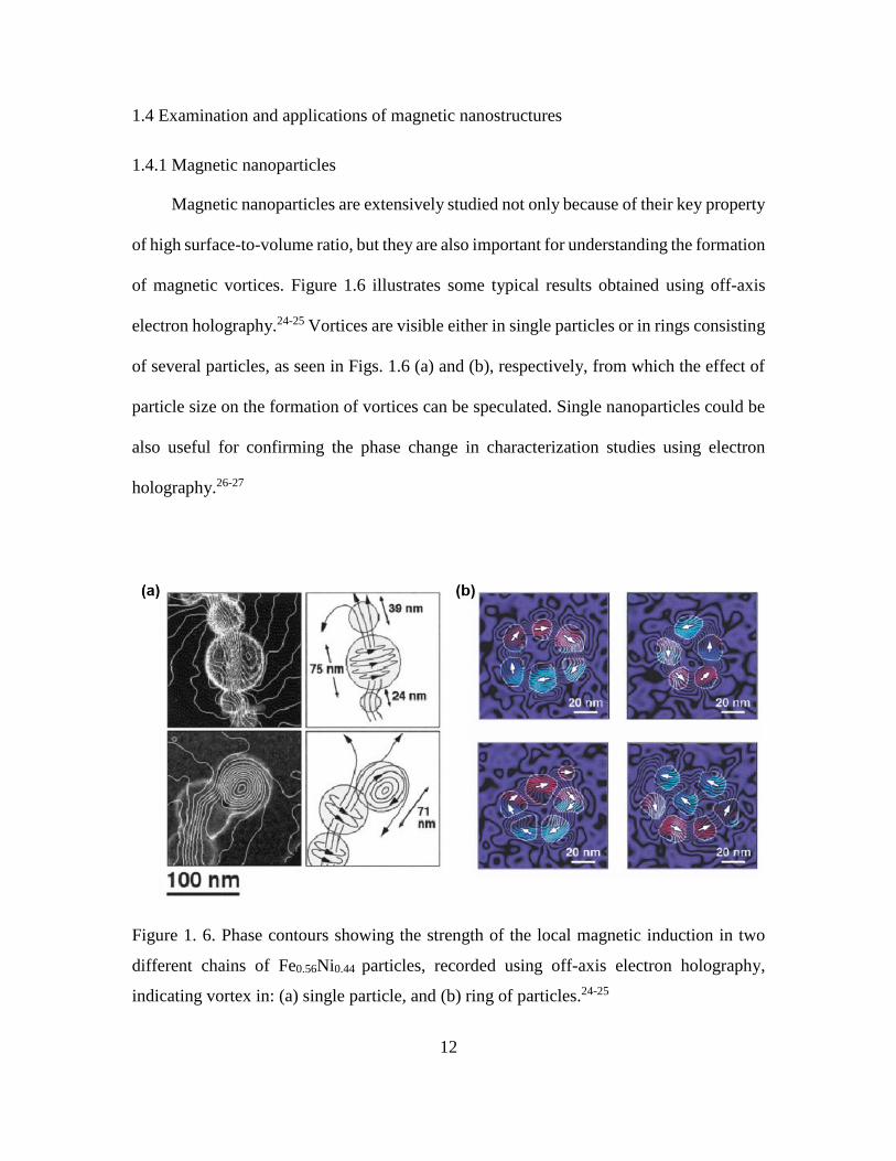
Magnetic nanoparticles are extensively studied not only because of their key property
of high surface-to-volume ratio, but they are also important for understanding the formation
of magnetic vortices. Figure 1.6 illustrates some typical results obtained using off-axis
electron holography.24-25 Vortices are visible either in single particles or in rings consisting
of several particles, as seen in Figs. 1.6 (a) and (b), respectively, from which the effect of
particle size on the formation of vortices can be speculated. Single nanoparticles could be
also useful for confirming the phase change in characterization studies using electron
holography.26-27
Figure 1. 6. Phase contours showing the strength of the local magnetic induction in two
different chains of Fe0.56Ni0.44 particles, recorded using off-axis electron holography,
indicating vortex in: (a) single particle, and (b) ring of particles.24-25

13
The ability to remotely control the spatial position of a nanoparticle while tracking
its motion in real time provides an exciting new tool for nanoscale sensing. Iron oxide or
iron oxide – gold particles are the most intensively developed magnetic nanoparticle
because they exhibit both magnetic and plasmonic behavior.28 As well as the property of
single magnetic particles, the behavior of a cluster or group of particles is more important
for biomedicine applications29 because manipulating the motion of nanoparticles is quite
challenging. Nano-sized particles are extremely susceptible to Brownian motion and the
inertial forces associated with their motion are negligible.
1.4.2 Magnetic nanowires and nanorods.
Manipulating the location of magnetic nanostructures is challenging. To improve the
control of magnetic structures and to assemble possible networks in desired locations,
various kinds of structure have been developed.
Magnetic nanowires consisting of ferromagnetic material are often prepared using
nanoporous track-etched polycarbonate membranes which are then filled by
electrodeposition.30 One interesting feature of magnetic nanowires is that they may contain
multiple magnetic domains along their long axis. This may be achieved by modifying the
wire morphology and adding antiferromagnetic or diamagnetic sections into the wire, as
shown by the example in Fig. 1.7.31

14
Figure 1. 7. (a) Hologram (acquired at 120 keV) and (b) associated remnant B map of a
Cu/CoFeB (50/50 nm) NW for a magnetic field applied parallel to the axis of the NW prior
to the hologram acquisition. 31
The multiple domain structure of nanowires could be used to represent binary
information as part of a memory device. Precise control of the domain wall between
adjacent recording bits would enable read-and-write processing in a nanowire-based device.
Based on this principle, Parkin and co-workers have proposed and developed the ‘racetrack
memory’ as an emerging technology for non-volatile magnetic random access memory.32
In the racetrack memory mechanism, the series motion of domain walls along a magnetic
nanowire shift register would be controlled using spin-polarized current pulses. The
physical effect in current-driven domain wall motion is based on a spin-momentum transfer
torque that is exerted by spin-polarized conduction electrons on the magnetic moments in
the wire, so that the domain wall moves as the torque rotates the moments, as illustrated in
Fig. 1.8.

15
Figure 1. 8. Schematic of racetrack memory using ferromagnetic nanowire in (a) vertical
configuration and (b) horizontal configuration. Data encoded as a pattern of magnetic
domains along a portion of the wire. Pulses of highly spin-polarized current move the entire
pattern of domain walls coherently along the length of the wire past read-and-write
elements.32
Using specific chemical processing methods, magnetic nanostructures, especially
nanoparticles, can be embedded in other materials. Heterostructured colloids composed of
semiconductor nano-rods tipped with magnetic or noble materials in either “matchstick”
or “dumbbell” topologies have received recent attention as a route towards well-defined 1-
D nanocrystals.33 Figure 1.9 illustrates the processing and morphology of CdSe and CdS
nanorods with cobalt nanoparticle tips with platinum core. From Figs. 1.9 (b) and (c), these
nanorods with ferromagnetic tips form a self-assembled square-shaped network which may
possibly be used for novel applications.33

16
Figure 1. 9. (a) Synthesis procedure for nanorods with cobalt (cobalt oxide) nanoparticle
‘tip’ with platinum core; (b) and (c) TEM images of low and high magnification showing
network consisting of nanorods.33
1.4.3 Magnetic structures for spin electronics
Electrons have charge and spin but, until recently, these were considered separately.
In classical electronics, charges are moved by electric fields to transmit information and
are saved in a capacitor for storage. In magnetic recording, magnetic fields are used to read
or write information stored by the magnetization, which ‘measures’ the local orientation of
spins in ferromagnets. A novel device mechanism where magnetization dynamics and
charge currents act on each other in nanostructured magnetic materials is being developed.

17
Ultimately, ‘spin currents’ could replace charge currents for the transfer and storage of
information, allowing faster, low-energy operations.34
Spintronic devices use polarized electrons as carriers. The advantages lie in the
combination of equilibrium magnetism and nonequilibrium spin to manipulate the minority
carrier population. Spin injection and detection could also achieve ideal switching.35 The
original concept of a spintronic device combines a ferromagnetic material with MOSFET
and diode, as shown as Fig. 1.10. In a spintronic diode, a ferromagnetic p-region would
hold the polarized electron in the conduction band with Zeeman splitting, and in a
spintronic MOSFET, the spin injector and detector would serve as the source and drain.
The magnetic field originating from the gate would control the channel switching.
Figure 1. 10. (a) Band structure of spintronic diode. (b) Schematic of spintronic
MOSFET.35
1.4.4 Patterned magnetic nanostructures
For the purposes of data recording applications, the ideal properties for patterned
media are well-defined remnant states, a reproducible magnetization reversal process and
a narrow switching field distribution. In practice, there are two major factors that affect the
magnetic response of patterned nanomagnets: size and anisotropy.36-37 Figure 1.11 is an

18
example of the effect of shape anisotropy and shows the magnetic induction map for a
patterned C-shaped Co structure at different stages of a hysteresis half cycle.
Figure 1. 11. Magnetic induction maps for C-shaped Cobalt nanostructure obtained using
electron holography.36
Another extensively studied type of patterned magnetic structure which could also
involve exchange coupling are nanopillars consisting of multilayer structures. Current-
induced magnetic reversal of nanopillars with perpendicular anisotropy and high coercive
fields holds great promise for faster and smaller magnetic bits in data-storage applications.
The best results have been observed for Co/Ni multilayers, which have larger giant
magnetoresistance values and spin-torque efficiencies than Co/Pt multilayers.38 Electron-
beam lithography is the general method used for processing patterned nanostructure
because the shape can be edited using computer programing. However, lithography
requires lift-out and has low productivity. Alternative methods using mask and ion-milling
on multilayer films deposited by DC magnetron sputtering have recently been developed
and widely used to generate nanopillars.39-40 This procedure is illustrated in Fig. 1.12.40

19
Figure 1. 12. Schematic illustration of method used to fabricate magnetic nanopillars.40
1.5 Outline of dissertation
The research of this dissertation has concentrated on the characterization of magnetic
nanostructures and devices using advanced electron microscopy techniques, especially off-
axis electron holography. Examples of work on similar types of material have already been
discussed in the preceding text.
This dissertation research can be roughly separated into three major parts, according
to different materials of interest: i) magnetic nanostructures; ii) thin-film ferrites; iii)
magnetic multilayers.
Chapter 1 has provided the motivation for this research and introduced some basic
physics concepts.
Chapter 2 summarizes important experimental aspects of this dissertation, including
growth methods, preparation of samples, and characterization methods.

20
Chapter 3 describes the characterization of magnetic properties of several different
types of magnetic nanostructures, including Co nanoparticles, Fe/GaAs shell/core
nanowires, carbon spiral with magnetic core and nanopillars consisting of Co/Pd
multilayers.
Chapter 4 describes an investigation of NiZnCo thin-film ferrites grown by a novel
spin-spray coating method, which showed the in-plane nature of the magnetization and a
multigrain magnetic domain structure. The major results from this specific research have
been published elsewhere.41
The research in Chapter 5 illustrates the magnetic domain structure of CoFe/Pd
multilayers. It was found that by changing the thicknesses of single layers, the
perpendicular magnetic anisotropy could be controlled. The results of this research have
been submitted for publication.42

21
References
1H. C. Oersted, Annals of Philosophy. 16, 273 (1820).
2F. Fiorillo, J. Magn. Magn. Mater. 157, 428 (1996).
3ITRS, “International Technology Roadmap for Semiconductors 2011, Emerging
Research Devices,” 2011.
4R. C. O’Handley, Modern Magnetic Materials, Wiley, New York (2000).
5J. C. Maxwell, Phil. Trans. R. Soc. A 155, 459 (1865). 6W. L. O’ Brien and B. P. Tonner, Phys. Rev. B 49, 21 (1994).
7R. Jungblut, R. Coehorn, M. T. Johnson, J. aan de Stegge and A. Reinders, J. Appl.
Phys. 75, 6659 (1994).
8R. Jungblut, R. Coehoorn, M. T. Jognson, Ch. Sauer, P. J. van der Zaag, A. R. Ball, Th.
G. G. M. Rijks, J. aan de Stegge and A. Reinders, J. Magn. Magn. Mater. 148, 300
(1995).
9E. H. M. van der Heijden, K. J. Lee, Y. H. Choi, T. W. Kim, H. J. M. Swagten, C. Y.
You, and M. H. Jung, Appl. Phys. Lett. 102, 102410 (2013).
10M. R. Scheinfein, J. Unguris, R. J. Celotta and D. T. Pierce, Phys. Rev. Lett. 63, 668
(1989).
11Néel. L, C. R. Acad. Sci. 241, 533 (1955).
12S. Foner, Rev. Sci. Inst. 27, 261 (1959).
13W. Webb, IEEE Trans. Mag. 8, 51 (1972).
14C. G. Shull, E. O. Wollan and W. C. Koehler, Phys. Rev. 84, 912 (1951).
15G. Schütz, W. Wagner, W. Wilhelm, P. Kienle, R. Zeller, R. Frahm and G. Materlik,
Phys. Rev. Lett. 58, 737 (1987).
16D. A. Allwood, G. Xiong, M. D. Cooke and R. P. Cowburn, J. Phys. D: Appl. Phys. 36,
2175 (2003).
17Z. Q. Qiu and S. D. Bader, Rev. Sci. Instrum. 71, 1243 (2000).
18Y. Martin and H. K. Wickramasinghe, Appl. Phys. Lett. 50, 1455 (1987).

22
19D. Rugar, H. J. Mamin, P. Guethner, S. E. Lambert, J. E. Stern, I. McFayden and T.
Yogi, J. Appl. Phys. 68, 1169 (1990).
20D. J. Smith, Ultramicroscopy 108, 159 (2008).
21J. N. Chapman, J. Appl. Phys.: D 17, 623 (1984).
22H. Hopster and H. P. Oepen, Magnetic Microscopy of Nanostructures, (Springer-Verlag
Berlin Heidelberg, 2005). P. 71.
23K. Ishizuka and B. J. Allman, Electron Microsc. 54, 191 (2005).
24R. E. Dunin-Borkowski, T. Kasama, A. Wei, S. L. Tripp, M. J. Hÿtch, E. Snoech, R.
J. Harrison, A. Putnis, Microsc. Res. Tech. 64, 390-402 (2004).
25M. J. Hÿtch, R. E. Dunin-Borkowski, M. R. Scheinfein, J. Moulin, C. Duhamel, F.
Mazaleyrat and Y. Champion, Phys. Rev. Lett. 91, 25 (2003).
26M. Beleggia and Y. Zhu, Philos. Mag. 83, 8 (2003).
27M. Beleggia and Y. Zhu, Philos. Mag. 83, 9 (2003).
28J. Lim and S. A. Majetich, Nano Today 8, 98-113 (2013).
29D. Nieciecka, K. Nawara, K. Kijewska, A. M. Nowicka, M. Mazur, P. Krysinski,
Bioelectrochemistry 93, 2-14 (2013).
30C. R. Martin, Chem. Mater. 8, 1739-1746 (1996).
31A. Akhtari-Zavareh, L. P. Carignan, A. Yelon, D. Ménard, T. Kasama, R. Herring, R.
E. Dunin-Borkowski, M. R. McCartney, and K. L. Kavanagh, J. Appl. Phys. 116, 023902
(2014);
32S. S. P. Parkin, M. Hayashi, L. Thomas, Science 320 190 (2008).
33L. J. Hill, M. M. Bull, Y. Sung, A. G. Simmonds, P. T. Dirlam, N. E. Richey, S. E.
DeRosa, I, Shim, D. Guin, P. J. Costanzo, N. Pinna, M. Willinger, W. Vogel, K. Char
and J. Pyun, ACS NANO 6, 10 (2012).
34C. Chappert, A. Fert and F. Nguyen Van dau, Nat. Mater. 6, 813 - 823 (2007).
35I. Žutić, J. Fabian, S. Das Sarma, Rev. Mod. Phys. 76, 323 (2004).
36K. He, D. J. Smith, and M. R. McCartney, J. Appl. Phys. 107, 09D307 (2010).

23
37K. He, D. J. Smith, and M. R. McCartney, J. Appl. Phys. 105, 07D517 (2009). 38S. Mangin, D. Ravelosona, J. A. Katine, M. J. Carey, B. D. Terris and E. E. Fullerton,
Nat. Mater. 5, 210 - 215 (2006).
39J. I. Martín, J. Nogué, K. Liu, J. L. Vicente and I. K. Schuller, J. Magn. Magn. Mater.
256, 449 (2003)
40K. Naito, H. Hieda, M. Sakurai, Y. Kamata and K. Asakawa, IEEE Trans. Magn. 38, 5
(2002).
41D. Zhang, N. M. Ray, W. T. Petuskey, D. J. Smith and M. R. McCartney, J. Appl. Phys.
116, 083901 (2014).
42Desai Zhang, Justin M. Shaw, David J. Smith and Martha R. McCartney, J. Magn. Magn.
Mater. 388, 16 (2015).

24
CHAPTER 2
EXPERIMENTAL DETAILS AND METHODS
This chapter provides a brief overview of the experimental techniques used for
sample preparation and observation in this dissertation research.
2.1 Material growth and sample preparation
2.1.1 Magnetron sputtering deposition
Transition metals like iron and cobalt in Row 4 of the Periodic Table are widely used
to provide ferromagnetism in magnetic structures. Sputter deposition is a highly efficient
method to deposit thin film of magnetic materials. This technique was first discussed by
Grove.1 Sputtering is initiated by the bombardment of energetic particles on the target.
These energetic particles are generally ions. It is straightforward to use an ion source aimed
towards the target, although an ion gun is not generally suitable for large-scale industrial
film deposition. Another source of ions is plasma. Typically, a cathode and an anode are
positioned opposed to each other in a vacuum chamber pumped to a base pressure on the
order of 1 10-4 Pa or lower. A noble gas (usually argon) is introduced into the chamber,
reaching a pressure between 1 and 10 Pa. When a high voltage in the range of 2 keV is
applied between the cathode and anode, a glow discharge is ignited. By applying this high
negative voltage to the cathode, positively charged ions are attracted from the plasma
toward the target.2 The deposition rate can be adjusted by changing the Ar pressure.
Different high voltage values are selected, depending on the type of metal that is deposited.
25
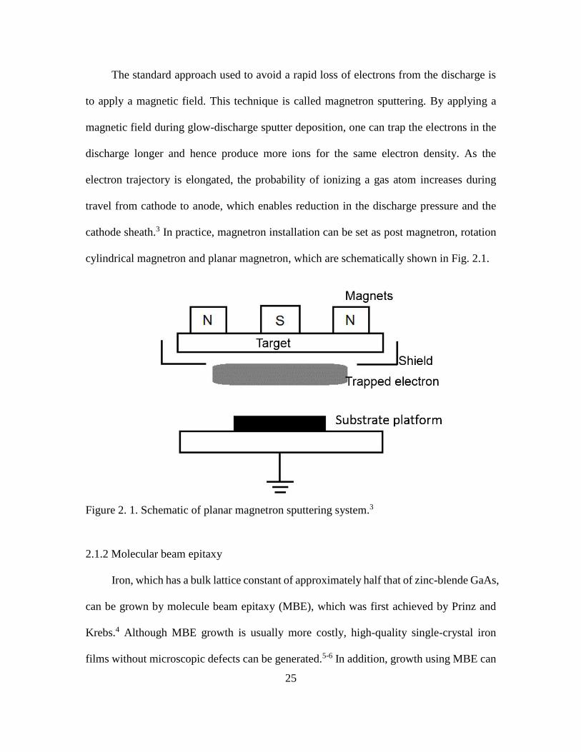
The standard approach used to avoid a rapid loss of electrons from the discharge is
to apply a magnetic field. This technique is called magnetron sputtering. By applying a
magnetic field during glow-discharge sputter deposition, one can trap the electrons in the
discharge longer and hence produce more ions for the same electron density. As the
electron trajectory is elongated, the probability of ionizing a gas atom increases during
travel from cathode to anode, which enables reduction in the discharge pressure and the
cathode sheath.3 In practice, magnetron installation can be set as post magnetron, rotation
cylindrical magnetron and planar magnetron, which are schematically shown in Fig. 2.1.
Figure 2. 1. Schematic of planar magnetron sputtering system.3
2.1.2 Molecular beam epitaxy
Iron, which has a bulk lattice constant of approximately half that of zinc-blende GaAs,
can be grown by molecule beam epitaxy (MBE), which was first achieved by Prinz and
Krebs.4 Although MBE growth is usually more costly, high-quality single-crystal iron
films without microscopic defects can be generated.5-6 In addition, growth using MBE can

26
be monitored and controlled using techniques such as reflection-high-energy electron
diffraction. Studies on Fe/GaAs(001) epitaxial structures have increased significantly over
the last two decades, largely due to the emergence of the fields of magnetoelectronics,
spintronics and in-plane magnetic anisotropy.7 The growth of Fe/GaAs(001) is an
extension of existing MBE techniques for growing magnetic material.
2.2 TEM sample preparation
For TEM characterization, the specimen needs to be thin enough to be electron-
transparent. Thus, nanostructures such as magnetic particles and nanowires can still be
observed directly when they are resting on TEM grids covered by carbon or SiN films.
Some types of nanostructures can be suspended in isopropanol and then simply placed onto
TEM grids by pipette.
Specimens grown on solid substrates are usually observed in cross-section and/or
plan-view geometry, which will require some sort of thinning. The thinning process often
starts with cleaving, and mechanical polishing, which is followed by dimpling to create
thinner areas of close to 10μm in thickness. Finally, the sample is argon-ion-milled to create
electron-transparent areas. In some cases, substrates such as commercial Si wafers are
strong enough, that the dimpling stage can be substituted. Alternatively, the wedge-
polishing technique can be used to create thin areas with thicknesses of close to 1μm. Thus,
the ion-milling time can be drastically reduced and possible defects generated from sample
preparation can be avoided, or at least minimized. The mechanical thinning procedure for
cross-section observation is schematically shown in Fig 2.2.

27
Figure 2. 2. Schematic of procedure used for preparing cross-section TEM samples.
The focused ion beam (FIB) is currently the most versatile technique for preparing
TEM samples. This technique has also been adopted for studying specimen in this
dissertation research. However, compared to the method illustrated in Fig. 2.2, samples
generated by FIB usually have smaller thin areas. Considering the size of magnetic
domains, which are typically on the order of several tens of nanometers, a comprehensive
characterization of magnetic induction distribution within a sample often demands more
thin area than FIB can provide. Moreover, the Ga beam used in the FIB thinning process
can cause sample damage as well as Ga implantation, which can seriously degrade any
magnetism present in the material.
2.3 Instrumentation
The transmission electron microscope (TEM) is a powerful instrument that allows
high-resolution imaging of materials over a wide range of magnifications up to the atomic
scale. Inside the TEM column, a beam of electrons is emitted by an electron gun,
accelerated by a high voltage, focused by electromagnetic condenser lenses, and then
28
transmitted through an ultrathin specimen. A TEM image is formed by an objective lens
from the electrons transmitted through the specimen, which is then magnified onto the final
imaging screen or detector. Images can be viewed on a fluorescent screen and recorded on
photographic film or by a charge-coupled device (CCD) camera. Alternatively, by using
the condenser lenses and the pre-field of the objective lens, a small probe at the Ångstrom
scale can be formed at the specimen plane. By scanning the focused probe across the
specimen, it is possible to obtain high-angle annular-dark-field (HAADF) images. Using a
large detector collection angle, the contrast in this imaging mode is dominated by Z-
contrast (Z = atomic number), meaning that the intensity I of the image is given roughly
by the expression I ∝ Zα where α ~ 1.4 – 1.7 depending on the inner collection angle.8
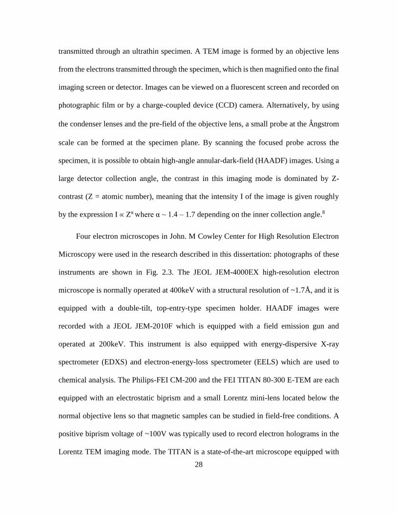
Four electron microscopes in John. M Cowley Center for High Resolution Electron
Microscopy were used in the research described in this dissertation: photographs of these
instruments are shown in Fig. 2.3. The JEOL JEM-4000EX high-resolution electron
microscope is normally operated at 400keV with a structural resolution of ~1.7Å, and it is
equipped with a double-tilt, top-entry-type specimen holder. HAADF images were
recorded with a JEOL JEM-2010F which is equipped with a field emission gun and
operated at 200keV. This instrument is also equipped with energy-dispersive X-ray
spectrometer (EDXS) and electron-energy-loss spectrometer (EELS) which are used to
chemical analysis. The Philips-FEI CM-200 and the FEI TITAN 80-300 E-TEM are each
equipped with an electrostatic biprism and a small Lorentz mini-lens located below the
normal objective lens so that magnetic samples can be studied in field-free conditions. A
positive biprism voltage of ~100V was typically used to record electron holograms in the
Lorentz TEM imaging mode. The TITAN is a state-of-the-art microscope equipped with

29
an X-FEG field emission gun and a CEOS image aberration corrector. This particular
microscope can be operated at 80, 200 and 300keV.
Figure 2. 3. Microscopes used for the majority of the research described in this dissertation.
2.4 Electron holography
2.4.1 Experimental settings
Off-axis electron holography is a powerful electron microscopy technique that
allows the amplitude and phase of the electron wave that has passed through a sample to
be determined, rather than its intensity, which is normally the case for TEM imaging.9 The
phase shifts of the electron wave deduced from reconstructed electron hologram can then
be used to provide quantitative information about the distribution of magnetic fields within
and outside the sample with a spatial resolution that can approach the nanometer scale
under optimal conditions.10

30
The basic experimental setting for off-axis electron holography for the CM-200 is
illustrated schematically in Fig. 2.4. The field emission gun (FEG) provides a coherent
source of electrons, the electrostatic biprism provides overlap of the object wave with the
vacuum (reference) wave, and the CCD camera permits quantitative hologram recording.
Figure 2. 4. (a) Schematic showing the essential TEM components for off-axis electron
holography, (b) Photo of CM-200 showing locations of key components.
As illustrated in Figs. 2.4 and 2.5, the recorded holography information is embedded
in the hologram which consists of interference fringes obtained by overlapping the object
wave with the vacuum or reference wave. The change in phase of the electron is represented
by the change in spacing and distribution of these fringes. The basic interaction between
an electron with electrostatic and magnetic fields can be expressed simply by the Lorentz
force as:
𝐅 = 𝑒(𝐄 + 𝐯 × 𝐁) (2.1)

31
where E is the electric field, v is the electron velocity and B is the magnetic induction.
The phase shift of an electron wave that has passed through the sample, relative to the
wave that has passed only through the vacuum, is given in one dimension by the
expression11:
ϕ(x) = CE ∫ V(x, z)dz −e
ℏ∬ B⊥(x, z)dxdz (2.2)
In equation 2.2, z is the incident beam direction, x is a direction in the plane of the
sample, V contains contributions to the potential from electrostatic fields and the mean
inner potential (MIP), 𝐵⊥is the component of the magnetic induction perpendicular to both
x and z, and CE is an constant that depends on the energy of the incident electron. Assuming
that neither V nor B vary with z within the sample thickness in small local areas, then the
expression for the phase can be simplified to:
ϕ(x) = CEV(x)t(x) −e
ℏ∫ B⊥(x)t(x)dx (2.3)
Differentiation with respect to x leads to an expression for the phase gradient of
d𝜙(𝑥)
dx= 𝐶𝐸
𝑑
𝑑𝑥[𝑉(𝑥)𝑡(𝑥)] −
𝑒
ℏ𝐵⊥(𝑥)𝑡(𝑥) (2.4)
Equations (2.3) and especially (2.4) are fundamental to the measurement and quantification
of magnetic induction using electron holography for phase imaging, as illustrated in Fig
2.5. Notice, if the sample is uniform in composition and thickness, then the term
CEd
dx[V(x)t(x)] in equation 2.4 is zero. Phase contributions from both electrostatic and
mean inner potentials can be solved in certain geometries, as will be discussed later. More
imaging theory for electron holography can be found in Refs. 12-14.

32
Figure 2. 5. Schematic illustration of the origin of the phase shifts studied by off-axis
electron holography.12
To quantify the in-plane magnetization within the sample, the phase contribution
from the MIP [V(x) t(x)] needs to be removed. Theoretically, if the sample thickness profile
can be obtained, it would be possible to calculate the MIP using the recorded amplitude
image but this requires knowledge of the electron inelastic mean-free-path (MFP) relevant
to specific acceleration voltages and the materials. Currently, there is a lack of MFP data,
making this method difficult to carry out.
One approach to obtaining the magnetic induction of the sample involves recording
a second hologram after reversely magnetizing the specimen to change the sign of the
magnetic induction.10 From equation 2.4, these two holograms will include the same MIP
contribution but opposite contributions from magnetic induction. By using half of the sum

33
and difference of the phase deduced from these two holograms, then the MIP and magnetic
contributions, respectively, can be separated and calculated. This approach can be easily
realized by tilting the sample and turning on the current in the objective lens. Since the
sample is located in the pole piece of the objective lens, the vertical magnetic field
originating from the objective lens will create an in-plane portion when the sample is tilted.
Turning on the objective-lens current after the sample is tilted also provides in situ
magnetizing of the sample. The tilt angle of the specimen holder can be read digitally from
the microscope control unit. Combined with prior calibration of the magnetic field as a
function of objective lens current, it is possible to determine the value of the in-plane
magnetic field exerted on the sample. Figure 2.6 shows the tilting procedure and magnetic
field – current (H-I) curve of objective lens. The curve shown in Fig. 2.6 (b) was previously
generated for the CM200 used in this dissertation.10 Fig. 2.6 (c) shows the calibrated curve
for the FEI TITAN similar to the one used in this dissertation, which is installed in
Technical University of Denmark. Both the CM200 and the TITAN 80-300 ETEM allow
tilting angles of up to 30o. According to their H-I curve, the objective lens can then provide
enough in-plane magnetic field to magnetize most magnetic materials into saturation.
Another approach is to acquire two holograms at different electron energies, which
according to equation 2.3 only affects the MIP contribution.15 However, in practice,
electron microscopes are usually optimally aligned and operated at their highest operation
voltage. Even after careful alignment to ensure that the microscope is fully functional at
lower voltage, electrons with lower voltage can only penetrate thinner samples causing loss
in observation area. In addition, the inelastic mean free path varies with electron energy,
so that the lack of data causes further complications for interpreting the MIP.

34
Figure 2. 6. (a) Schematic diagram showing the use of specimen tilt to provide the in-plane
component of the applied field needed for in situ magnetization reversal experiments; (b)
and (c) Hall probe measurement of magnetic field in the specimen plane of Philips CM200
and TITAN as a function of objective lens current.10
Finally, it should be noted that this approach of inverting magnetism in the sample
may fail when the magnetization within the sample does not reach exactly opposite states.
35
An alternative approach to solve this problem is by flipping the sample over. By reversing
the direction of the vector v in equation 2.1, the Lorentz force will be reversed, in turn
causing opposite phase contribution. Chapter 4 will provide an example in more detail.
2.4.2 Processing of phase maps
From equation 2.3, magnetic information about the sample is embedded in the phase
distribution. Thus, the electron phase shift needs to be extracted from the original hologram.
Figure 2.7 illustrates an example of this phase extraction using an AlFeNiCo alloy sample.
This material is not related to the research of this dissertation but it provides very strong
magnetic signals which are suitable for demonstration purposes.
A hologram is obtained by superimposing a reference wave on an object wave. This
superimposition region is filled with interference fringes which contain both amplitude and
phase information. Figure 2.7 (a) shows an example of hologram obtained from the
AlFeNiCo sample. Bending of the interference fringes is visible within the sample, caused
either by magnetic induction or an abrupt change in MIP. The bending can be observed
more clearly in the enlargement shown in Fig. 2.7 (b), taken from the position indicated by
the dashed box in Fig. 2.7 (a). A Fast Fourier Transform (FFT) is carried out using the
desired region of the hologram, to produce a central auto-correlation peak and two
sidebands in reciprocal space. To remove phase changes caused by the illumination and
recording systems, another hologram is recorded from vacuum using the same illuminating
conditions. Dividing the FFT of the original hologram by the FFT of this reference
hologram, characteristic phase and amplitude information of the sample can be obtained,
as indicated in Fig. 2.7 (c). The central auto-correlation peak contains Fourier transform of
uniform intensity of the reference wave and the intensity distribution of a normal TEM

36
image. The two sidebands contain identical information apart from a change in sign of the
phase. One of these two sidebands is selected using a numerical aperture to obtain the
desired phase information. The sideband selection must be done carefully to avoid overlap
with the streak of the central peak which results from Fresnel diffraction. Smaller
interference-fringe spacing obtained by increasing the biprism voltage can achieve full
separation of the side bands in reciprocal space. However, an increase in biprism voltage
also results in a decrease in fringe contrast. An aperture with a wavy mask edge is often
used in practice to extract the desired sideband. The complex image is reconstructed by
obtaining an Inverse Fast Fourier Transform (IFFT) of the extracted sideband, as indicated
in Fig. 2.7 (d). The IFFT here is applied on both sample and reference sidebands, then the
resulting complex images are divided to normalize the amplitude and subtract any phase
shifts associated with the biprism or the illumination. The phase information can be
retrieved from the reconstructed complex image by taking 𝑎𝑟𝑐𝑡𝑎𝑛𝑖
𝑟, where i and r are the
imaginary and real part of the complex image, followed by unwrapping any phase
discontinuities that result from the fact it is initially calculated modulo 2π. The
reconstructed phase images can be expressed in the pseudo-color mode, as shown in Fig.
2.7 (e), where different colors represent equal phase value. Figure 2.7 (e) is referred to as
a phase map in this dissertation. As illustrated by the color coding shown in Fig. 2.7 (g),
the color sequence corresponds to each phase increase by 2π. The relative phase change
relevant to different positions in the phase map can be determined. Amplitude information
can be retrieved by calculating√𝑖2 + 𝑟2 . As mentioned above, it is possible from the
inelastic electron MFP to calculate the thickness of the observed area using amplitude
information. On the other hand, it is sometimes useful to estimate the relative thickness

37
variation within the sample by assuming constant MFP, as shown in the thickness map in
Fig. 2.7 (f).
Figure 2. 7. Image reconstruction for extracting phase and amplitude information from
hologram of AlFeNiCo alloy.
The color scheme for the relative phase change, as shown in Fig. 2.7, is very useful
for determining the direction and gradient of the phase shift, i.e., the magnetic induction
distribution can be obtained as a phase gradient vector map using equation 2.4 and pseudo-
color phase map. Figure 2.8 shows an example of obtaining the magnetic induction map

38
from the phase map shown in Fig. 2.7 (e). Magnetization components along the directions
indicated by arrows 1 and 2 perpendicular to each other are obtained by taking derivatives
with respect to the corresponding normal orientations, as shown in Fig. 2.8 (b) and (c),
respectively. By combining two orthogonal gradient vectors in Fig. 2.8 (b) and (c) by
calculating the modulus, then a gradient vector map can be generated, as shown in Fig. 2.8
(d). The directions of the vectors are encoded using a specific RGB color scheme, as shown
in Fig. 2.8 (e). The relationship between directions and colors is indicated by the color
wheel shown in Fig. 2.8 (f). Some dark stripe features within the magnetic domains are
visible in Fig. 2.8 (e) which do not correspond to any in-plane directions. These areas may
include only out-of-plane magnetization.
The magnitude of the vector can be obtained using amplified phase contour lines.
The amplitude of the magnetic induction can then be estimated from the density of the
contour lines. An example with more details is given in Chapter 5.
Signal-to-noise ratio is one of the key features determining the phase resolution of
holography.16 One drawback of the above procedure is that noise in the hologram will be
present in the final phase map. When placing an aperture to select sidebands, the noise
from the original hologram is inevitably included. Since the noise appears randomly, it is
difficult to subtract it using FFT operation. In practice, the most effective way to limit the
noise is averaging multiple holograms to improve the signal-to-noise ratio.

39
Figure 2. 8. (a) Reconstructed phase image of AlFeNiCo alloy in Pseudo-color mode
showing relative phase change; (b) and (c) gradient of phase, directions of derivatives are
marked by black arrows 1 and 2 in (a); (d) Phase gradient vectors map; (e) Magnetic
induction map using RGB color to encode the directions; (f) Color wheel indicating relation
between colors and directions of the magnetic induction.

40
References
1W. R. Grove, Phil. Trans. R. Soc. Lond. 142, 87 (1852).
2 K. Wasa and S. Hayakawa, Handbook of Sputter Deposition Technology, Noyes, New
Jersey (1992).
3P. M. Martin, Handbook of Deposition Technologies for Films and Coatings, Elsevier,
Burlington (2010)
4G. A. Prinz and J. J. Krebs, Appl. Phys. Lett. 39, 397 (1981).
5 H, Schönherr, Richard Nötzel, W, Ma and K. H. Ploog, J. Appl. Phys. 89, 169 (2001).
6L. R. Fleet, K. Yoshida, H. Kobayashi, Y. Kaneko, S. Matsuzaka, Y. Ohno, H. Ohno, S.
Honda, J. Inoue and A. Hirohata, Phys. Rev B 87, 024401 (2013).
7G. Wastlbauer and J. Bland, Adv. Phys. 54, 137 (2005).
8S.Hillyard and J. Silcox, Ultramicroscopy, 58, 6 (1995).
9M. R. McCartney and D. J. Smith, Annu. Rev. Mater. Res. 37, 729 (2007).
10R. E. Dunin-Borkowski, M. R. McCartney, B. Kardynal, S. S. P. Parkin, M. R.
Scheinfein, and D. J. Smith, J. Microsc. 200, 187–205 (2000).
11M. R. McCartney, N. Agarwal, S. Chung, D. A. Cullen, M. Han, K. He, L. Li, H.
Wang, L. Zhou, D. J. Smith, Ultramicroscopy, 110, 375-382 (2010).
12D. J. Smith and M. R. McCartney, Introduction to Electron Holography, Edited by E.
Völkl, L. F. Allard and D. C. Joy, Kluwer Academic-Plenum Publisher, New York,
Chapter 4 (1999).
13H. Lichte, P. Formanek, A. Lenk, M. Linck, C. Matzeck, M. Lehmann and P. Simon,
Annu. Rev. Mater. Res. 37, 539 (2007).
14A. Tonomura, Surf. Sci. Rep. 20, 317 (1994).
15A. Tonomura, Rev. Mod. Phys. 59, 639 (1987).
16F. Lenz, Optik 79, 13 (1988).
41
CHAPTER 3
EXAMINATION OF MAGNETIC NANOSTRUCTURES
Magnetic nanostructures with sizes in the range of 2–10 nm are of much interest in
many different areas, including magnetic fluids, catalysis, data storage, medicine delivery
and magnetic resonance imaging (MRI). The technique of off-axis electron holography
represents a powerful approach for studying such magnetic nanostructures. This chapter
describes four examples which illustrate the procedures used to reveal and quantify
magnetic fields using electron holography.
3.1 Co nanoparticles
Cobalt nanoparticles (NPs) were provided for examination by the group of Professor
Pyun at University of Arizona. These NPs were prepared by thermal deposition via the
chemical reaction:1
𝐶𝑜2(𝐶𝑂)8 + 𝐶18𝐻38 → 𝐶𝑜 + 𝐻2 + 𝐶𝑂𝑥 + 𝐶𝐻𝑦
Under Ar gas atmosphere, 1.04g of cobalt octacarbonyl Co2(CO)8 dissolved in 3ml 1, 2-
dichlorobenzene (DCB) for 30 min was rapidly injected at 180 C into 20 mL of air-free
octadecene (C18H38) containing 0.67m mol of oleylamine under vigorous stirring. The
resulting solution was reacted at 180oC for 20 min. In order to oxidize the Co NPs, the
colloidal solution was reacted chemically at 250oC or 300oC for 12 hours under the mixture
of dry oxygen and argon gas. Particles were placed in acetone and transferred onto uniform
carbon films supported on TEM grid.
The morphology of the Co NPs is shown in Fig. 3.1. Figure 3.1 (a) indicates that the
NP sizes ranged from 10 to 20nm. The particles tend to clump together as clusters or chains
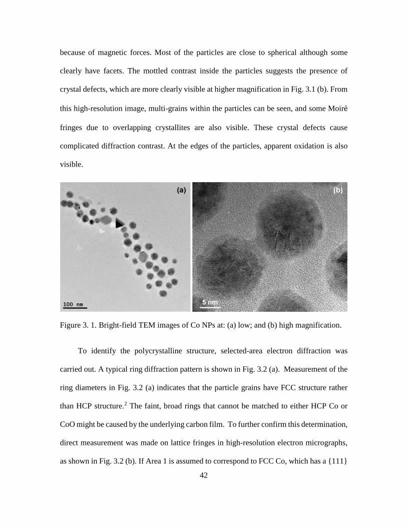
42
because of magnetic forces. Most of the particles are close to spherical although some
clearly have facets. The mottled contrast inside the particles suggests the presence of
crystal defects, which are more clearly visible at higher magnification in Fig. 3.1 (b). From
this high-resolution image, multi-grains within the particles can be seen, and some Moiré
fringes due to overlapping crystallites are also visible. These crystal defects cause
complicated diffraction contrast. At the edges of the particles, apparent oxidation is also
visible.
Figure 3. 1. Bright-field TEM images of Co NPs at: (a) low; and (b) high magnification.
To identify the polycrystalline structure, selected-area electron diffraction was
carried out. A typical ring diffraction pattern is shown in Fig. 3.2 (a). Measurement of the
ring diameters in Fig. 3.2 (a) indicates that the particle grains have FCC structure rather
than HCP structure.2 The faint, broad rings that cannot be matched to either HCP Co or
CoO might be caused by the underlying carbon film. To further confirm this determination,
direct measurement was made on lattice fringes in high-resolution electron micrographs,
as shown in Fig. 3.2 (b). If Area 1 is assumed to correspond to FCC Co, which has a {111}

43
lattice-fringe spacing of 2.05 Å, then Area 2 has a lattice-fringe spacing of 2.19 Å, and Area
3 has a lattice-fringe spacing of 2.56 Å. Area 2 would most likely correspond to the CoO
{200} reflection which has a spacing of 2.13 Å and Area 3 would correspond to CoO {111}
which has a spacing of 2.46 Å. Thus, these results are consistent with fcc Co NPs with thin
CoO shells.
Figure 3. 2. (a) Selected-area electron diffraction pattern from Co nanoparticles; (b) High-
resolution phase contrast image of a single Co NP used for lattice-spacing measurement.
In holography observations of these Co NPs, the samples were magnetized in situ
using the magnetic field of the objective lens of the CM200. With the sample tilted by 30o,
the lens current was increased to 1000mA, providing an in-plane magnetic field of ~1 T
along the direction of the sample tilt.3 The objective lens was turned off and the sample
was tilted back to the horizontal position. Holograms were then recorded using the Lorentz
mini-lens with the specimen in a field-free condition. Knowing that the chain magnet will
have magnetic anisotropy along its long axis, the sample can be easily magnetized by tilting
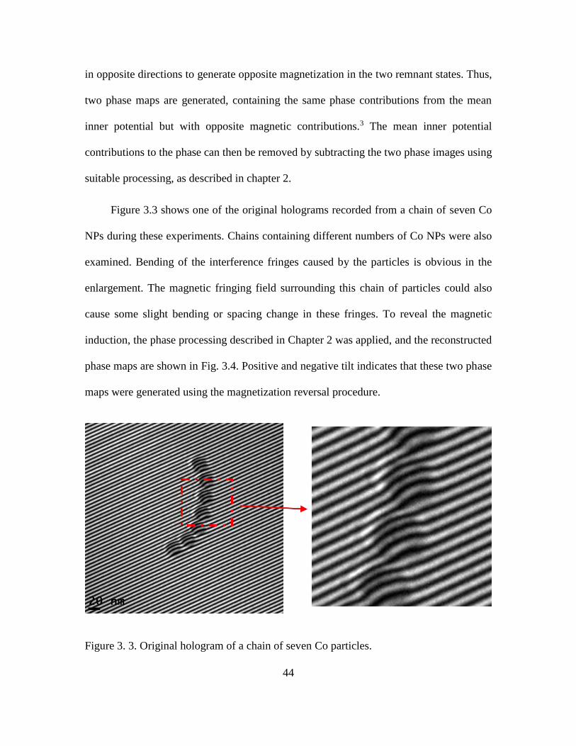
44
in opposite directions to generate opposite magnetization in the two remnant states. Thus,
two phase maps are generated, containing the same phase contributions from the mean
inner potential but with opposite magnetic contributions.3 The mean inner potential
contributions to the phase can then be removed by subtracting the two phase images using
suitable processing, as described in chapter 2.
Figure 3.3 shows one of the original holograms recorded from a chain of seven Co
NPs during these experiments. Chains containing different numbers of Co NPs were also
examined. Bending of the interference fringes caused by the particles is obvious in the
enlargement. The magnetic fringing field surrounding this chain of particles could also
cause some slight bending or spacing change in these fringes. To reveal the magnetic
induction, the phase processing described in Chapter 2 was applied, and the reconstructed
phase maps are shown in Fig. 3.4. Positive and negative tilt indicates that these two phase
maps were generated using the magnetization reversal procedure.
Figure 3. 3. Original hologram of a chain of seven Co particles.

45
The two color maps in Fig. 3.4 show reversal of color on the two opposite sides of
the chain, thus representing reversal of the magnetic induction. Since the phase change is
perpendicular to the chain, the magnetic field must be aligned along the chain. From
measurements of the two profiles, the magnetic induction from this NP chain creates a
phase change of about 0.42 rad.
Figure 3. 4. (a) and (b) Phase maps generated using opposite tilting technique; (c) and (d)
corresponding line profiles from the positions indicated by square boxes in (a) and (b),
respectively.
Based on the saturation value of B for Co of 1.7 T,4-7 the expected phase change due
to magnetic induction from the chains of Co NPs can be calculated. For simplicity, the Co
particles are modeled as spheres and curving of the chain is ignored. The calculation was
done with Cartesian coordinates with the y axis along the chain. The phase contribution
can be expressed as:
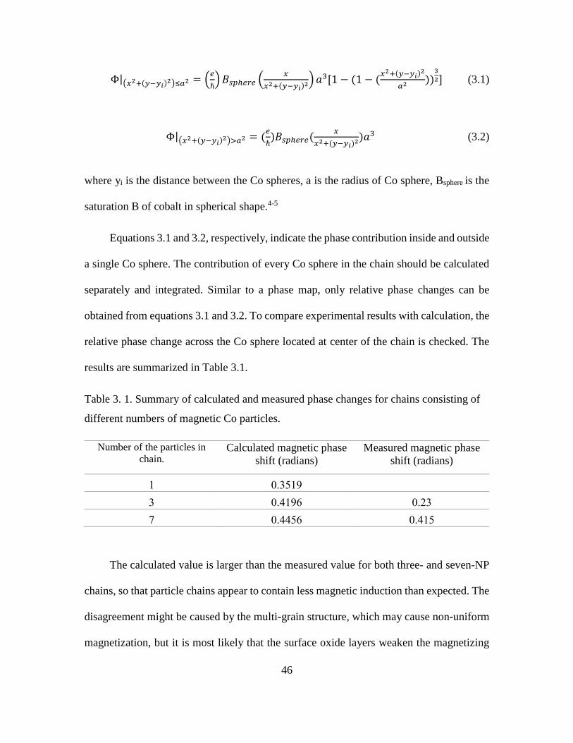
46
Φ|(𝑥2+(𝑦−𝑦𝑖)2)≤𝑎2 = (𝑒
ℏ) 𝐵𝑠𝑝ℎ𝑒𝑟𝑒 (
𝑥
𝑥2+(𝑦−𝑦𝑖)2) 𝑎3[1 − (1 − (𝑥2+(𝑦−𝑦𝑖)2
𝑎2 ))3
2] (3.1)
Φ|(𝑥2+(𝑦−𝑦𝑖)2)>𝑎2 = (𝑒
ℏ)𝐵𝑠𝑝ℎ𝑒𝑟𝑒(
𝑥
𝑥2+(𝑦−𝑦𝑖)2)𝑎3 (3.2)
where yi is the distance between the Co spheres, a is the radius of Co sphere, Bsphere is the
saturation B of cobalt in spherical shape.4-5
Equations 3.1 and 3.2, respectively, indicate the phase contribution inside and outside
a single Co sphere. The contribution of every Co sphere in the chain should be calculated
separately and integrated. Similar to a phase map, only relative phase changes can be
obtained from equations 3.1 and 3.2. To compare experimental results with calculation, the
relative phase change across the Co sphere located at center of the chain is checked. The
results are summarized in Table 3.1.
Table 3. 1. Summary of calculated and measured phase changes for chains consisting of
different numbers of magnetic Co particles.
Number of the particles in
chain. Calculated magnetic phase
shift (radians)
Measured magnetic phase
shift (radians)
1 0.3519
3 0.4196 0.23
7 0.4456 0.415
The calculated value is larger than the measured value for both three- and seven-NP
chains, so that particle chains appear to contain less magnetic induction than expected. The
disagreement might be caused by the multi-grain structure, which may cause non-uniform
magnetization, but it is most likely that the surface oxide layers weaken the magnetizing

47
effect. Although Bsphere already includes the effect of demagnetizing field of sphere,4-5 the
difference between the calculated and measured values differs more for the case of the
three-NP chain, most likely because of the greater effect of the demagnetizing field which
has not been estimated correctly. No obvious phase change was observed across the single
sphere. The phase change related to a single sphere might be too small to be detected.
Moreover, a magnetic vortex could possibly form in a single sphere, which would not cause
any phase change cross it.8-9
3.2 Core/shell magnetic nanowires
Ferromagnetic nanowires (NWs) with nanoscale diameter are of interest because of
their potential applications in magnetic recording and storage, and also because of the novel
behavior that is predicted for magnetic materials with dimensions that approach the atomic
scale.10-12 Using electron holography, the remanent states of magnetic NWs consisting of
ferromagnetic material has been successfully studied.13 In this present example,
GaAs/Fe/Au core/shell NWs were studied by electron holography. This novel geometry
could possibly generate magnetic anisotropy by control of the Fe layer thickness. The
samples were provided by the group of Professor Furdyna at Notre Dame, and the detailed
growth procedure can be found in references [14-15].
Two sets of NWs were grown in these experiments. One set was grown on GaAs
(111)B substrates, and the other was grown on GaAs (110) substrates. Scanning electron
microscopy (SEM) images confirmed the NW morphology, as shown in Figs. 3.5 (a) and
(b), respectively. The GaAs NWs grew on (111)B Zincblende (ZB) GaAs with their growth
axis normal to the substrate. Due to the preferred direction of epitaxial growth, the NWs
grown on (110) substrates had an inclination of ~ 35.3o with respect to the substrate normal.

48
This inclination is visible in Fig. 3.5 (b), where the NWs are imaged with the substrate in
plan-view geometry. It was later discovered that this tilting of the NWs grown on (110)
substrates resulted in rotationally non-uniform Fe coating rather than uniform coating, as
observed for the NWs grown on (111)B substrates.
Figure 3. 5. SEM images of GaAs/Fe/Au core/shell NWs grown on ZB GaAs: (a) (111)B,
and (b) (110), respectively.
The macroscopic magnetic properties of these core/shell NWs were measured by
ferromagnetic magnetic resonance (FMR) and small-angle neutron scattering (SANS).16
The FMR technique was carried out to check the NWs grown on (110) substrate with the
sample mounted such that the magnetic field could be rotated full circle in the (110) plane.
The angular dependence of the resonance field (Hres) of NWs is shown in Fig. 3.6, where
35o and 215o correspond to H pointing along the NWs, 0o and 90o correspond to H pointing
perpendicular and parallel to substrate surface. From Fig. 3.6, two spectrum sets are visible,
as marked by “x” and “o”. The resonance field marked “x” reaches minimum and
maximum, which correspond to field orientation parallel and perpendicular to the wires,
consistent with demagnetization fields of the elongated NW geometry. The resonances

49
marked “o” show maxima at 0o and 180o, consistent with fringing field of a flat magnetic
plate with a normal along those directions, which could be ascribed to Fe film coating the
surface of the substrate.
Magnetic contributions from the NW shells and coating on the substrate will overlap
if the wires are perpendicular to the substrate when using the FMR technique. To
discriminate between these two contributions, the SANS technique was applied with the
magnetic field perpendicular to the NW growth direction. The incident neutron beam had
a propagation vector parallel to the wire growth direction, and was polarized to be
alternately spin-up (+) or spin-down (-) with respect to H. The scattered beam intensity I
was measured as a function of scattering vector Q. Using a wide-angle polarized 3He
neutron, allows detection of spin-flip scattering I+- and I-+ and indicating the presence of
wire magnetization parallel to the NW growth direction.17-18 Figure 3.7 shows the sum of
the measured I+- and I-+ signals, and reveals no statistically significant scattering. Thus, in
a magnetic field perpendicular to the NWs, the SANS measurements demonstrated that the
wires exhibit magnetization along the field direction, with no detectable axial component.
To determine the relation between the magnetic domain structure and magnetic anisotropy,
electron holography characterization of individual NWs is thus required.

50
Figure 3. 6. Angular dependence of the resonance field (Hres) of GaAs/Fe/Au Core/Shell
NWs grown on (110) substrate.16
Figure 3. 7. SANS data of NWs grown on (111)B substrate: Sum of the spin-flip
scattering (+- and -+).16

51
It is anticipated that iron can grow epitaxially on ZB GaAs since their respective
lattice spacings are 2.86Å and 5.65Å, so that an atomically-matched interface can be
constructed.15 Corresponding TEM images of these nanowires are shown in Fig. 3.8, where
uniform and non-uniform metal coatings are clearly visible. The Fe shell does not appear
to grow as a uniform epitaxial layer and metal clusters are also visible. The clear absence
of this epitaxial coating can be understood by referring to Fig. 3.9. Figure 3.9 (a) shows the
core of GaAs NW, which primarily has the Wurtzite (WZ) structure, as well as containing
many stacking faults. This defective core structure will not permit epitaxial Fe growth.
Furthermore, detailed observations of the shell regions, as shown in Fig. 3.9 (b), indicate
only Au lattice fringes but no Fe is visible.
Growth of the WZ phase often takes place preferentially when using the vapor-liquid-
solid (VLS) growth.19 Stacking-fault-free ZB GaAs NW growth can be achieved by locally
reducing vapor supersaturation and limiting growth speed.20 To explain formation of the
WZ phase in these NWs, cross-section TEM images of NWs grown on (111)B ZB GaAs
standing on the substrate were taken, as shown in Fig. 3.10. Between NWs and original ZB
GaAs substrate, a buffer layer of thickness about 500 nm is visible. Figure 3.11 shows a
high-resolution TEM image from the bottom area of an NW, which indicates that the GaAs
buffer grew with high density of stacking faults. These would make GaAs transform to the
WZ phase and the NWs could adopt this structure. In some locations, GaAs remains in the
ZB phase and grows to the top surface of the buffer layer, as shown in Fig. 3.12. Two ZB
structure grains are visible in Fig. 3.12, with arrows that indicate the lattice direction in
each grain. However, these limited areas of the ZB phase can only be found in the gap

52
between NWs and do not support NW growth. In addition, Figs. 3.11 and 3.12 indicate that
the metal coating on the substrate has a similar morphology as the shell layer of the NW.
Figure 3. 8. TEM images of GaAs/Fe/Au core/shell NWs grown on: (a) (111)B and (b)
(110) ZB GaAs, respectively.
Figure 3. 9. High-resolution TEM images of GaAs/Fe/Au core/shell NWs: (a) GaAs core
showing highly defective WZ structure. (b) shell region with Au 2.35 Å lattice fringes
visible.

53
Figure 3. 10. Bright field cross-section TEM image of GaAs/Fe/Au core/shell sample
including NWs, buffer layer, and substrate.
Figure 3. 11. High-resolution cross-section TEM image near the bottom part of a
GaAs/Fe/Au core/shell NW.

54
Figure 3. 12. Cross-section TEM image showing highly defective top surface of buffer
layer with ZB GaAs phase. Lattice direction in each grain indicated by arrows.
To check for the presence of Fe, EDXS line scans were carried out, as shown in Fig.
3.13. The line profile shows the presence of Fe signal overlapping with the Au shell
suggesting Au/Fe is formed. However, an oxygen signal is also detected overlapping with
iron, indicating that all or part of the iron was oxidized. However, even if all of the iron in
the shell is oxidized, Fe3O4 and γ-Fe2O3 can still hold magnetic moments.
To further identify the type of iron oxide, one needs a technique such as electron-
energy-loss spectrum (EELS) to discriminate chemical bonds or quantify the atomic ratio
between elements. The Gatan EELS detector on the JEOL 2010F was used to record the
EELS spectrum shown in Figure 3.14. Different types of iron oxide can be resolved by
different shapes of fine structure of the oxygen K-edge.21 However, this fine structure was
not successfully revealed in these experiments. Instead, the Gatan EELS analysis package
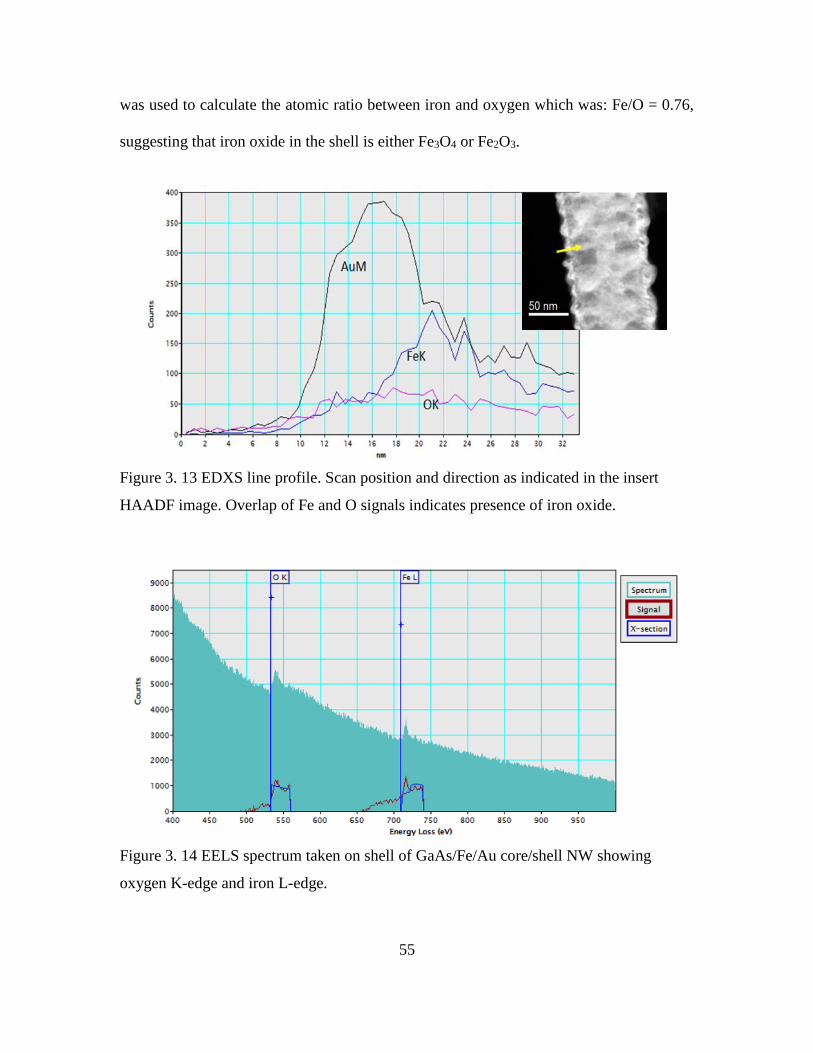
55
was used to calculate the atomic ratio between iron and oxygen which was: Fe/O = 0.76,
suggesting that iron oxide in the shell is either Fe3O4 or Fe2O3.
Figure 3. 13 EDXS line profile. Scan position and direction as indicated in the insert
HAADF image. Overlap of Fe and O signals indicates presence of iron oxide.
Figure 3. 14 EELS spectrum taken on shell of GaAs/Fe/Au core/shell NW showing
oxygen K-edge and iron L-edge.

56
The magnetic nature of the NWs was characterized by off-axis electron holography.
Corresponding phase maps of the two types of NWs are shown in Fig. 3.15. Reconstructed
phase maps show no sign of any fringing magnetic field around nanowires grown on
(111)B substrates [Fig. 3.15 (a)]. On the other hand, a phase jump typically of about 3 rad
is visible across NWs grown on (110) substrates [Fig 3.15 (b)]. Based on these results, it
appears that NWs grown on (111)B substrates have cylindrical shells with magnetic fields
confined within the shell and forming closed loops. In effect, these NWs display an
intriguing toroidal-shape field geometry, which would seem to warrant further
investigation. To examine the possibility that iron (iron oxide) in the shell is
nanocrystalline and below the limit of superparamagnetism, NWs grown on (111)B were
checked at liquid nitrogen temperature, which is lower than the Néel temperature of iron
or iron oxide. Phase maps generated at liquid nitrogen temperature again did not show any
sign of magnetism.
Figure 3. 15. Phase maps of Au/Fe/GaAs shell/core nanowires grown on (a) (111)B and (b)
(110) ZB GaAs. The directions of magnetic field used to magnetize the sample are
indicated.
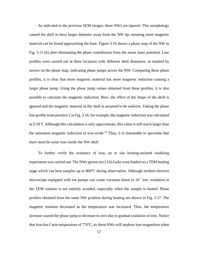
57
As indicated in the previous SEM images, these NWs are tapered. This morphology
caused the shell to have larger diameter away from the NW tip, meaning more magnetic
material can be found approaching the base. Figure 3.16 shows a phase map of the NW in
Fig. 3.15 (b) after eliminating the phase contribution from the mean inner potential. Line
profiles were carried out at three locations with different shell diameters, as marked by
arrows on the phase map, indicating phase jumps across the NW. Comparing these phase
profiles, it is clear that more magnetic material has more magnetic induction causing a
larger phase jump. Using the phase jump values obtained from these profiles, it is also
possible to calculate the magnetic induction. Here, the effect of the shape of the shell is
ignored and the magnetic material in the shell is assumed to be uniform. Taking the phase
line profile from position 2 in Fig. 3.16, for example, the magnetic induction was calculated
as 0.59 T. Although this calculation is only approximate, this value is still much larger than
the saturation magnetic induction of iron oxide.22 Thus, it is reasonable to speculate that
there must be some iron inside the NW shell.
To further verify the existence of iron, an in situ heating-assisted oxidizing
experiment was carried out. The NWs grown on (110) GaAs were loaded on a TEM heating
stage which can heat samples up to 800oC during observation. Although modern electron
microscope equipped with ion pumps can create vacuums down to 10-7 torr, oxidation in
the TEM column is not entirely avoided, especially when the sample is heated. Phase
profiles obtained from the same NW position during heating are shown in Fig. 3.17. The
magnetic moment decreased as the temperature was increased. Thus, the temperature
increase caused the phase jump to decrease to zero due to gradual oxidation of iron. Notice
that Iron has Curie temperature of 770oC, so these NWs will anyhow lose magnetism when

58
heated to 800oC. However, after the holder was cooled down to room temperature, the NWs
were fully magnetized again but no phase jump was visible, verifying that magnetism
decreased because of oxidation.
Figure 3. 16 Phase map of GaAs/Fe/Au core/shell NW after eliminating phase contribution
from mean inner potential (left), line profiles from positions marked by arrows in phase
map (right).
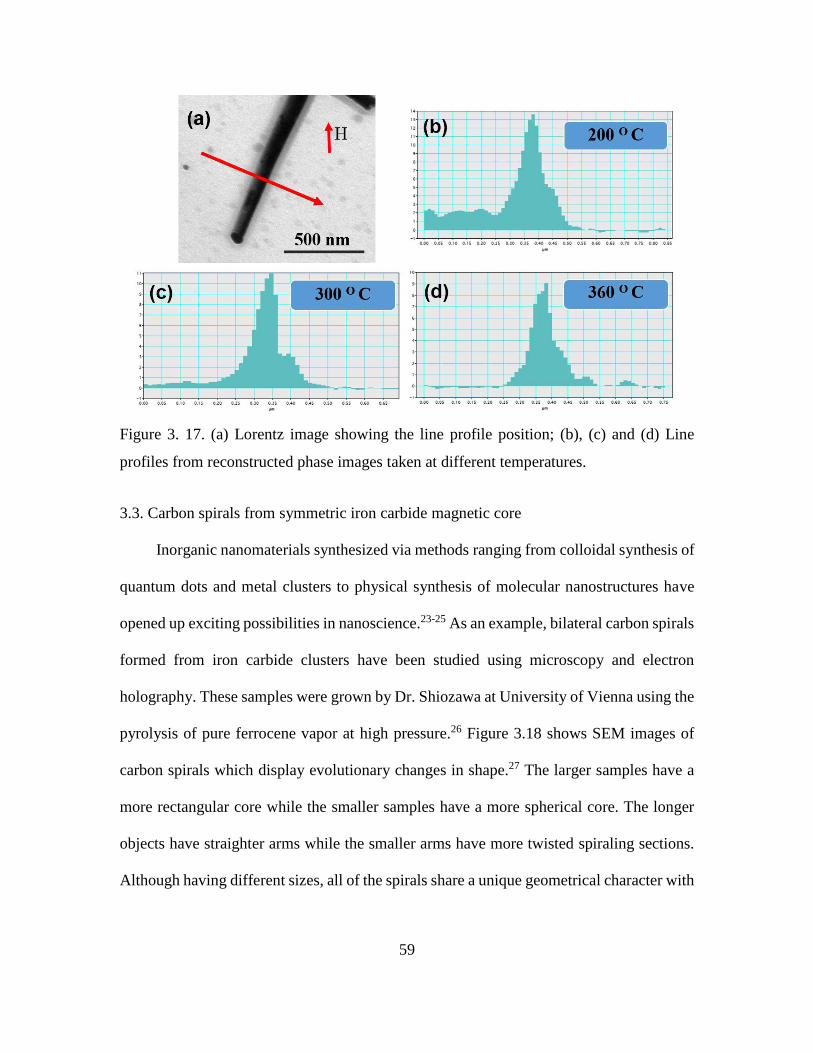
59
Figure 3. 17. (a) Lorentz image showing the line profile position; (b), (c) and (d) Line
profiles from reconstructed phase images taken at different temperatures.
3.3. Carbon spirals from symmetric iron carbide magnetic core
Inorganic nanomaterials synthesized via methods ranging from colloidal synthesis of
quantum dots and metal clusters to physical synthesis of molecular nanostructures have
opened up exciting possibilities in nanoscience.23-25 As an example, bilateral carbon spirals
formed from iron carbide clusters have been studied using microscopy and electron
holography. These samples were grown by Dr. Shiozawa at University of Vienna using the
pyrolysis of pure ferrocene vapor at high pressure.26 Figure 3.18 shows SEM images of
carbon spirals which display evolutionary changes in shape.27 The larger samples have a
more rectangular core while the smaller samples have a more spherical core. The longer
objects have straighter arms while the smaller arms have more twisted spiraling sections.
Although having different sizes, all of the spirals share a unique geometrical character with
60
reflectional symmetry. This morphology stands out in contrast to growth of carbon
nanotube where sp2 carbon layers grow unilaterally from one side of the catalyst only.
Figure 3. 18. SEM images of carbon spirals of different sizes. Bright contrast at center of
each spiral correspond to Fe-rich catalyst particle.27
Due to the large dimensions of these carbon spirals, applying TEM characterization
to these structure is difficult because only small spirals are transparent to electrons. Figure
3.19 shows a TEM image and the corresponding selected-area electron diffraction (SAED)
from a small spiral. As indicated in the TEM image, small spirals with twist shape form
from the iron carbide core. SAED at the core region shows the diffraction pattern of
cementite (Fe3C) in [112] zone axis, as visible in Fig. 3.19 (b). Figure 3.19 (c) shows the
SAED pattern from the carbon arm, indicating that the arm has no long-range crystalline
order. Some mottled contrast is visible within the carbon arm, which is due to small iron
carbide clusters accidentally deposited on the surface during the synthesis process.

61
Figure 3. 19. (a) TEM image of carbon spirals formed from iron carbide core; (b) and (c)
SAED from the areas marked in (a).
Due to the geometry of the Lorentz lens imaging mode, about only 20 percent of
electrons are used for imaging compared to the regular TEM mode, making the sample
appear to be less electron-transparent. Thus, when checking the carbon spirals, no
information can be extracted from within the carbon arm. Figure 3.20 shows reconstructed
phase maps from different locations of one carbon spiral. The corresponding Lorentz image
of the same spiral is also shown in order to identify the locations. Figure 3.20 (b) shows
uniform phase distribution around the tip of the carbon spiral indicating no fringing
magnetic field originated from the tip. Equal phase for the carbon arm shown in Fig. 3.20
(c) indicates no magnetic induction along the arm. Figures 3.20 (d) and (e) show local
phase variations around the core part of the carbon spiral. Based on the relation between

62
phase distribution and magnetic induction explained in Chapter 2, this phase distribution
can be interpreted as being caused by three magnetic domains, which are schematically
illustrated in Fig. 3.20 (f). Thus, Figure 3.20 overall indicates that the Fe3C core behaves
as a ferromagnet and includes multiple magnetic domains, whereas the carbon arm does
not hold any magnetization.
Figure 3. 20. (a) Lorentz image of carbon spirals; (b), (c), (d) and (e) Phase maps generated
on different locations marked in (a); (f) Schematic of magnetic field lines that can possibly
cause the phase distribution in (d).
3.4 Magnetic nanopillars
Materials that show magnetic anisotropy normal to the film surface hold great
promise for smaller and faster magnetic media in data-storage devices. As mentioned in
Chapter 1, multilayer structures with exchange coupling are strong candidates for this

63
application. If data storage is considered as a digital procedure, then magnetic storage bits
consisting of nanopillars become attractive.28 Although several studies have provided
deeper understanding of the interaction between electrons and multilayer magnetization
that gives rise to effects such as GMR,29-31 the practical use of such technologies requires
that the speed and efficiency of spin-torque switching of the magnetic element is improved
so that high-anisotropy, thermally stable bits can be reliably written. Thus, the
magnetization of nanopillars in the remnant state has been investigated using electron
holography.
The nanopillars studied here were grown on Si substrates and consisted of multilayers
with the structure Ta(2nm)/[Co(0.2nm)/Pd(0.7nm)]5/Fe(1.5nm)/[Pd(0.7nm)/Co (0.2
nm)]5/ Pd(1nm). These samples were provided by the group of Professor Fullerton at
University of California, San Diego. The method used for sample growth is illustrated in
Fig. 3.21. To further study the magnetic anisotropy of these nanopillars, two sets of sample
were prepared, namely ‘ref’ and ‘80deg’, as shown in Fig. 3.22. The sample ‘ref’ was
processed by Ar milling perpendicular to the substrate, while sample ‘80deg’ was
processed with Ar milling inclined at 80 degree to the substrate.
To carry out TEM characterization, samples were prepared in both cross-section and
plan-view geometry, and by wedge polishing and dimpling, respectively. Final thinning
was achieved by Ar ion-milling. Cross-section TEM images are shown in Fig. 3.23. From
low magnification micrographs, Figures 3.23(a) and (b), it is clear that the nanopillars are
successfully fabricated. The heights of the pillars and the separations between the pillars
are basically identical in these two sets of samples. The plan-view TEM images shown in

64
Fig. 3.23 indicate that the pillars have no regular shape, although the side walls are often
faceted. However, there are no obvious difference between the ‘ref’ and ‘80deg’ samples.
Diffraction contrast from within the pillar suggests a multigrain structure and the presence
of crystalline defects. High-resolution TEM images indicate differences in morphology
caused by different milling process. The side walls of pillars in ‘ref’ set are perpendicular
to substrate, while the side walls of ‘80deg’ have a slight slope, as shown in Figs. 3.23 (c)
and (d).
Figure 3. 21. Schematic illustration of processing two sets of nanopillars.
Figure 3. 22. Plan-view TEM images of (a) ‘ref’ and (b) ‘80deg’ nanopillars.

65
Figure 3. 23. Cross-section TEM image of ‘ref’ nanopillars in (a) low and (c) high
magnification; Cross-section TEM image of ‘80deg’ nanopillars in (b) low and (d) high
magnification.
For the holography observations, all samples were magnetized in situ using the
objective lens while the sample was tilted by 30 degrees. The out-of-plane and in-plane
magnetization directions for cross-section and plan-view samples are illustrated in Fig.
3.24. Since the pillar spacings can be obtained from the plan-view image, it is possible to
determine the number of pillars observed in the projection geometry once the Si thickness
is known. Using amplitude images and the known mean free path of Si,32-33 it is possible
to estimate the thickness of the areas observed.
Reconstructed phase maps of both samples in cross-section and plan-view geometries
are shown in Fig. 3.25 and Fig. 3.26. The pillars are small in size so that only one or two
interference fringes cover a single pillar (to obtain enough contrast, the fringe spacing
could not be decreased too much), making the pillars insufficiently resolved in phase maps

66
for the cross-section geometry. However, the region of vacuum near the pillars is flat
indicating no out-of-plane fringing field emerging from the top surface. In the cross-section
phase map, some irregular features caused by diffraction, sample bending or thickness
variation, are visible in the silicon substrate. From the phase maps in plan-view geometry,
most pillars are resolved. However, there is again no visible sign of any magnetism within
the sample. Moreover, the flat phase in vacuum area also suggests that no magnetic field
is present.
Figure 3. 24. Schematic of directions of magnetic field for in situ magnetizing.
Figure 3. 25. Phase maps of ‘ref’ nanopillars in: (a) cross-section, and (b) plan-view
geometry.

67
Figure 3. 26. Phase maps of ‘80deg’ nanopillars in: (a) cross-section, and (b) plan-view
geometry.
Measurements carried out on the original wafers using the VSM technique showed
that the remnant magnetic induction could reach as high as 1 T. Such strong magnetic
induction would be expected to create distinct phase changes in the holography
observations. The reason(s) for the absence of any phase change in the holography studies
is unclear at this time. Sample preparation seems the most likely possibility. A complicated
multilayer structure embedded in a pillar of small size could be easily damaged by ion-
milling. Since the magnetic signal is supposed to be generated by exchange coupling
between the multilayers, any damage to the multilayer structure would also destroy the
magnetic anisotropy. Moreover, the magnetic anisotropy might not be strong enough and
could possibly be degraded by the magnetic field of the objective lens.
To recover the magnetic anisotropy, a degaussing procedure was recommended by
our expert colleague. This procedure was carried out using oscillating electronic magnets.
The magnets provided an original magnetic field of 0.8 T, with decreasing amplitude of
0.1 T for every oscillation. Each period of oscillation took about 3 s. The degaussing
magnetic field is also applied in both ‘in plane’ and ‘out of plane’ directions, which is

68
indicated in Fig. 3.24. To avoid saturating the magnetization, the objective lens was
switched off when samples were inserted into the microscope for holography observation.
Sample tilting and microscope aligning were done in field-free Lorentz mode only.
Figure 3.27 shows phase maps taken after degaussing in field-free condition. Based
on the discussions about Fig. 3.25 and 3.26, these results demonstrate that no magnetic
induction or anisotropy was recovered. The samples were then re-magnetized using the
objective lens which provided ~0.7 T ‘out of plane’ and ‘in plane’ magnetic field for cross-
section and plan-view samples, respectively. No magnetism was revealed by phase maps:
these phase maps are omitted here.
Figure 3. 27. Phase maps after degaussing operation: (a) 'ref' sample in cross-section
geometry, (b) '80deg' sample in cross-section geometry, (c) '80deg' sample in plan-view
geometry.

69
Since the damage caused by sample preparation seem like the most likely reason that
causes the missing magnetism, MFM measurements were also done on raw wafers in field-
free conditions, and the results are shown in Fig. 3.28 and 3.29. The MFM developed for
these samples was a modified atomic force microscope (AFM) with a cobalt tip which can
reveal ‘out of plane’ magnetic field. Figure 3.28 (a) shows MFM scan on ‘ref’ sample
surface. Besides some scan noise, the features in MFM scan are caused by surface
morphology which can be found in AFM scan from the same area, which is shown in Fig.
3.28 (b). No obvious feature corresponding to magnetism is visible in Fig. 3.28 (a). Figure
3.39 shows MFM and AFM scans of the ‘80deg’ sample from a larger area. Similar to Fig.
3.28, the contrast variation in MFM scan is due to surface morphology that is also present
in the AFM scan. Although the detection limit of MFM is lower than electron holography,34
the MFM results demonstrate that there is no strong ‘out-of-plane’ magnetic anisotropy.
Figure 3. 28. (a) MFM scan, and (b) AFM scan of 'ref' sample.

70
Figure 3. 29. (a) MFM scan, and (b) AFM scan of '80deg' sample.
Finally, holography experiments were done with an applied magnetic field. With the
objective lens current turned up to 2000 mA and the sample tilted to 35 degree, there was
approximately 3000 Oe ‘out of plane’ magnetic field applied to the cross-section sample.
For the CM200, 2000 mA is the max current that the objective lens can hold while imaging
in Lorentz mode because objective lens will create a new crossover in electron beam path,
making it impossible to focus when the objective lens is so strong. However, according to
the hysteresis loop measured by VSM, which is shown in Fig. 3.30, 3000 Oe should be
enough to magnetize the ‘80deg’ sample to saturation. One of the Lorentz images taken in
such condition is shown in Fig. 3.31. Because of the sample tilt, the overlapped pillars are
visible in projection. The generated phase map is shown in Fig. 3.32. All three rows of
pillars are resolved in the phase map. However, the flat phase distribution in the vacuum
indicates there is no fringing field in either ‘out-of-plane’ or ‘in-plane’ directions.
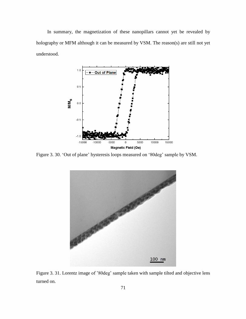
71
In summary, the magnetization of these nanopillars cannot yet be revealed by
holography or MFM although it can be measured by VSM. The reason(s) are still not yet
understood.
Figure 3. 30. ‘Out of plane’ hysteresis loops measured on ‘80deg’ sample by VSM.
Figure 3. 31. Lorentz image of ’80deg’ sample taken with sample tilted and objective lens
turned on.
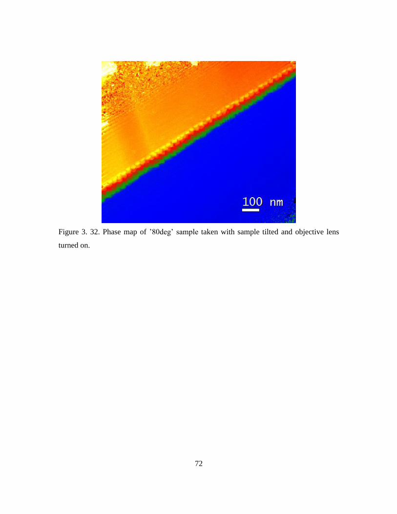
72
Figure 3. 32. Phase map of ’80deg’ sample taken with sample tilted and objective lens
turned on.

73
References
1J. S. Hong, J. Pyun, Y. W. Park, C. S. Kim and I. Shim, IEEE Trans. Magn. 45, 2464
(2009).
2C. Petit, Z. L. Wang, and M. P. Pileni, J. Phys. Chem. B 109, 15309-15316 (2005).
3R. E. Dunin-Borkowski, M. R. McCartney, B. Kardynal, S. S. P. Parkin, M. R.
Scheinfein, and D. J. Smith, J. Microsc. 200, 187–205 (2000).
4M. Beleggia and Y. Zhu, Philos. Mag. 83, 8 (2003).
5M. Beleggia and Y. Zhu, Philos. Mag. 83, 9 (2003).
6C. Phatak, R. Pokharel, M.Beleggia and M. De Graef, J. Magn. Magn. Mater. 323, 2912-
2922 (2011).
7M. De Graef, N. T. Nuhfer and M. R. MCCartney, J. Microsc. 194, 1 (1999).
8R. E. Dunin-Borkowski, T. Kasama, A. Wei, S. L. Tripp, M. J. Hÿtch, E. Snoech, R. J.
Harrison, A. Putnis, Microsc. Res. Tech. 64, 390-402 (2004).
9M. J. Hÿtch, R. E. Dunin-Borkowski, M. R. Scheinfein, J. Moulin, C. Duhamel, F.
Mazaleyrat and Y. Champion, Phys. Rev. Lett. 91, 25 (2003).
10P. Gambardella, A. Dallmeyer, K. Maiti, M. C. Malagoli, W. Eberhardt, K. Kern, and
C. Carbone, Nature, 416, 301 (2002).
11F. J. Himpsel, J. E. Ortega, G. J. Mankey, and R. F. Willis, Adv. Phys. 47, 511 (1998).
12M. Weinert and A. J. Freeman, J. Magn. Magn. Mater. 38, 23 (1983).
13E. Snoeck, R. E. Dunin-Borkowskia, F. Dumestreb, P. Renaud, C. Amiens, B. Chaudret
and P. Zurcher, Appl. Phys. Lett. 82, 1 (2003).
14A. Rudolph, M. Soda, M. Kiessling, T. Wojtowicz, D. Schuh, W. Wegscheider, J.
Zweck, C. Back, and E. Reiger, Nano Lett. 9, 3860 (2009).
15K. Tivakornsasithorn, R. E. Pimpinella, V. Nguyen, X. Liu, M. Dobrowolska, and J. K.
Furdyna, J. Vac. Sci. Technol. 30, 02B115 (2012).
16R. E. Pimpinella, D. Zhang, M. R. McCartney, D. J. Smith, K. L. Krycka, B. J. Kirby,
B. J. O'Dowd, L. Sonderhouse, J. Leiner, X. Liu,M. Dobrowolska and J. K. Furdyna, J.
Appl. Phys. 113, 17B520 (2013).

74
17K. Krycka, J. Borchers, Y. Ijiri, R. Booth and S. Majetich, J. Appl. Crystallogr.
45, 554 (2012).
18W. C. Chen, R. Erwin, J. W. McIver III, S. Watson, C. B. Fu, T. R. Gentile, J. A.
Borchers, J. W. Lynn, and G. L. Jones, Physica B 404, 2663 (2009).
19F. Glas, J. Harmand and G. Patriarche, Phys. Rev. Lett. 99, 146101 (2007).
20H. Shtrikman, R, Popovitz-Biro, A. Kretinin and M, Heiblum, Nano Lett. 9, 215 (2009).
21C. Colliex, T. Manoubi and C. Orbiz, Phys. Rev. B 44, 11402 (1991).
22G. W. Rathenau, Rev. Mod. Phys. 25, 297 (1953).
23H. W. Kroto, J. R. Heath, S. C. O’Brien, R. F. Curl and R. E. Smalley, Nature 318, 162
(1985).
24S. Iijima, Nature 354, 56 (1991).
25K. S. Novoselov, A. K. Geim, S. V. Morozov, D. Jiang, Y. Zhang, S. V. Dubonos, I. V.
Grigorieva and A. A. Firsov, Science 306, 666 (2004).
26H. Shiozawa, A. Skeldon, D. Lloyd, V. Stolojan, D. Cox and S. Silva, Nano Lett. 11,
160 (2011).
27H. Shiozawa, A. Bachmatiuk, A. Stangl, D. Cox, S. Silva, M. Rümmeli and T. Pichler,
Sci. Rep. 3, 1840 (2013).
28S. Mangin, D. Ravelosona, J. A. Katine, M. J. Carey, B. D. Terris and E. E. Fullerton,
Nat. Mater. 5, 210 - 215 (2006).
29J. C. Slonczcewski, J. Magn. Magn. Mater. 247, 324–338 (2002).
30L. Berger, Phys. Rev. B 72, 100402 (2005).
31J. Barnas, A. Fert, M. Gmitra, I. Weymann and V. K. Dugaev, Phys. Rev. B 72, 024426
(2005).
32T. M. Chou and M. Libera, Ultramicroscopy, 94, 31-35 (2003).
33M. R. McCartney, M. Gajdardziska-Josifovska, Ultramicroscopy, 53, 283-289 (1994).
34H. Lichte, Ultramicroscopy 108, 256-262 (2008).

75
CHAPTER 4
CHARACTERIZATION OF DOMAIN STRUCTURE IN THIN FILM OF
NANOCRYSTALLINE Ni-Zn-Co SPINEL FERRITE
This chapter reports a microscopic study of the magnetic domain structure of
nanocrystalline thin films of nickel-zinc ferrite using transmission electron microscopy and
holography. The ferrite films were synthesized by Dr. Nicole Ray in the laboratory of
Professor William Petusky at Arizona State University, using aqueous spin-spray coating
and showed high complex permeability in the GHz range.1 The films consisted of columnar
grains with uniform chemical composition. Off-axis electron holography combined with
magnetic force microscopy in remanence indicated a multigrain domain structure with in-
plane magnetization but the magnetization showed no preferred distribution. The results
present here, which have also been published elsewhere,2 are focusing on microscopic
observations. Dr. Ray is credited with material development and macroscopic function.1
4.1 Introduction
Soft ferrite materials, such as those based on nickel-zinc-ferrite compositions, are of
interest because of their relatively low loss characteristics at high frequencies.3 Due to
technological needs, their applications are being pushed to even higher frequencies into
regimes where magnetic properties exhibit limitations. This behavior is often marked by
what is referred to as Snoek’s Limiting Law, which inversely correlates low frequency
permeability, µ’, and resonance frequency, f, as a product, i.e., (µ’ -1) f, that is usually
constant for a given material structure class and composition.1,3 This constancy is generally
independent of microstructure and other processing related characteristics, where

76
permeability might decrease because of porosity and cracking, and the resonance frequency
correspondingly increases.
These observations tend to hold for ferrite materials with polycrystalline structures
comprising of grains that are relatively large in size, on the order of near-sub-micron scales
or larger. Increases in the Snoek’s product are found in materials where the grain sizes are
substantially in the nanometer and mesoscopic scales (i.e., 10-100 nm).1,4 Matsushita, Abe
and others have reported such combination of properties on extremely fine grained films
of nickel-zinc-ferrite materials that are produced using an aqueous spray deposition
technique that they pioneered.4 For instance, the Snoek’s product for one of their
Ni0.28Zn0.18Fe2.54O4 films is calculated to be about 26.6 GHz, whereas it is about 1-3 GHz
for a bulk ferrite of similar composition.5 In addition, aqueous spray deposition also has
unique advantage of low temperature processing, making this technique possible to be
directly applied on printing circuit board (PCB) or antenna devices.
A detailed explanation of the behavior of nickel-zinc ferrites must correlate
comparative structures of the magnetic domains relative to the physical grain structure. In
large-grained materials, well-defined, multiple magnetic domains are observed within
individual physical grains.3,6 Magnetic domain boundaries interior to nanometer-scaled
grains are likely to be too energetic to be prevalent, so that either single magnetic domains
are defined concurrently with the physical grains or the magnetic domains must be spread
out over multiple physical grains.3,6
This chapter reports a comparison of the magnetic domain structure to the physical
grain structure of nickel-zinc-cobalt ferrite films, as imaged by transmission electron

77
microscopy, off-axis electron holography, and atomic force microscopy. The original
motivations for this study were to discover whether multi-grained magnetic domains could
be directly observed in these materials, or whether the magnetic domains were confined to
the physical grain structure.
4.2 Experimental details
The ferrite thin films in this work were deposited using a method similar to that
developed by Abe and Tamaura.7-8 Different materials were used as substrates, which were
heated to 90oC during the spin-spray process. In this work, we studied samples with
composition of approximately Ni0.20Zn0.60Co0.05Fe2.15O4 that were deposited on silicon and
glass substrates. Details of the processing conditions are reported elsewhere.1 Some of the
ferrite films were also deposited directly onto TEM grids with carbon support films:
however, only clusters were observed after deposition, indicating that a smooth surface
was essential for successful use of the spin-spray coating process. The real µ’ and
imaginary µ’’ permeabilities were measured as a function of frequency using a vector
network analyzer with a customized microstrip permeameter.9
For cross-section TEM and off-axis electron holography characterization, samples
were prepared using cutting, mechanical polishing, followed by dimpling to create thin
areas with total thicknesses of about 10μm. Final thinning was done by low energy (~3keV)
argon-ion-milling giving thin electron-transparent areas of about 200nm in thickness.
Samples in the plan-view geometry were also prepared, with dimpling and ion-milling done
only from the back side of the wafer. JEOL JEM-4000EX operated at 400keV with
interpretable resolution of 1.7Å was used for conventional diffraction-contrast and high-

78
resolution phase-contrast imaging, JEOL JEM-2010F operated at 200keV was used for
annular-dark-field (ADF) imaging and elemental analysis using energy-dispersive X-ray
spectroscopy (EDXS), and FEI CM-200 operated at 200keV was used for off-axis electron
holography observations. This last instrument is equipped with a field emission electron
gun that provides a highly coherent electron source and it has a Lorentz mini-lens located
beneath the normal objective lens so that samples can be studied in field-free conditions.
Magnetic force microscopy, MFM, measurements were done on the sample surfaces. The
equipment used was a home-built atomic force microscope (AFM) which has a cobalt
needle probe with a magnetic fringing field that is parallel to the long axis of the needle.
This magnetic field interacts with the magnetic field perpendicular to the sample surface
and reveals the out-of-plane magnetic domain structure.
4.3 Results and discussion
4.3.1 Sample permeability
Figure 4.1 shows the real and imaginary parts of the complex permeability spectrum
of a typical spin-coating film prepared in this study.1 The purpose of measuring the
complex permeability is for use in the comparison of Snoek’s Limiting Law. This law states
that there is a theoretical limit to the ferromagnetic resonance frequency: however, this
value can be exceeded using non-traditional processing techniques.1,3,5,10-13 The materials
characterized in this study exceeded the theoretical resonance frequency value for
conventional nickel-zinc ferrite.1,3,5 The Snoek’s product for our deposited film is
calculated to be 20.1 GHz, which is on the same order of magnitude as the films deposited
by Abe et al. The imaginary permeability has a value of around 20 in the GHz range, and
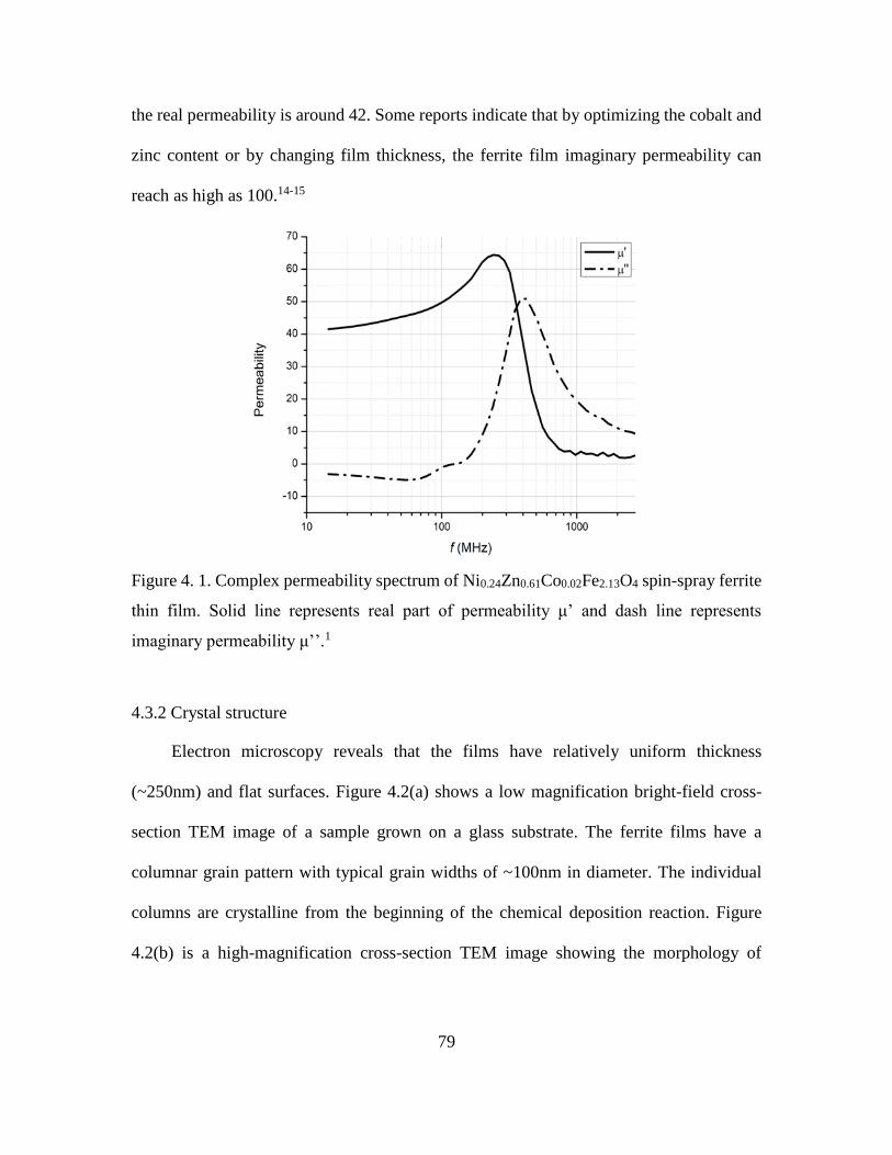
79
the real permeability is around 42. Some reports indicate that by optimizing the cobalt and
zinc content or by changing film thickness, the ferrite film imaginary permeability can
reach as high as 100.14-15
Figure 4. 1. Complex permeability spectrum of Ni0.24Zn0.61Co0.02Fe2.13O4 spin-spray ferrite
thin film. Solid line represents real part of permeability μ’ and dash line represents
imaginary permeability μ’’.1
4.3.2 Crystal structure
Electron microscopy reveals that the films have relatively uniform thickness
(~250nm) and flat surfaces. Figure 4.2(a) shows a low magnification bright-field cross-
section TEM image of a sample grown on a glass substrate. The ferrite films have a
columnar grain pattern with typical grain widths of ~100nm in diameter. The individual
columns are crystalline from the beginning of the chemical deposition reaction. Figure
4.2(b) is a high-magnification cross-section TEM image showing the morphology of
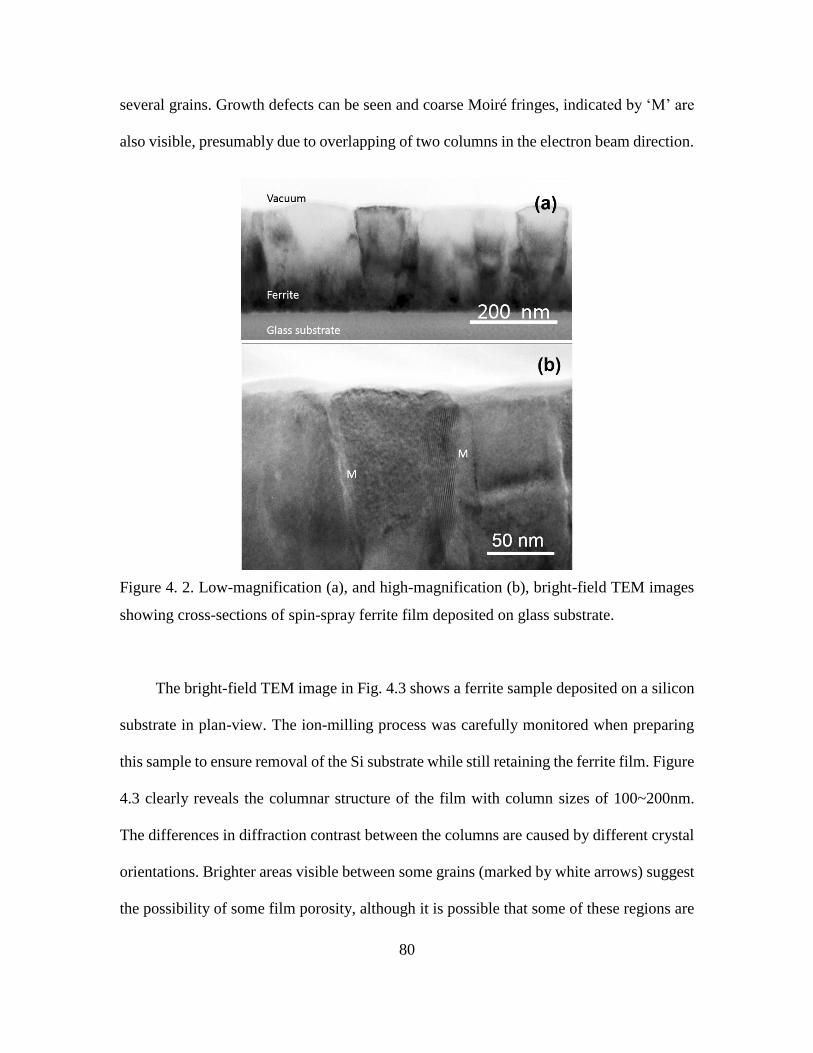
80
several grains. Growth defects can be seen and coarse Moiré fringes, indicated by ‘M’ are
also visible, presumably due to overlapping of two columns in the electron beam direction.
Figure 4. 2. Low-magnification (a), and high-magnification (b), bright-field TEM images
showing cross-sections of spin-spray ferrite film deposited on glass substrate.
The bright-field TEM image in Fig. 4.3 shows a ferrite sample deposited on a silicon
substrate in plan-view. The ion-milling process was carefully monitored when preparing
this sample to ensure removal of the Si substrate while still retaining the ferrite film. Figure
4.3 clearly reveals the columnar structure of the film with column sizes of 100~200nm.
The differences in diffraction contrast between the columns are caused by different crystal
orientations. Brighter areas visible between some grains (marked by white arrows) suggest
the possibility of some film porosity, although it is possible that some of these regions are

81
caused by the ion-milling process. Some mottling is also visible within single columns
(crystal grains) again suggesting the presence of crystal defects such as dislocations and
stacking faults.
Figure 4. 3. Plan-view bright-field TEM image showing spin-spray ferrite deposited on
silicon substrate. Arrows indicate possible porosity within the film.
4.3.3. Chemical composition.
Annular-dark-field images generated by scanning transmission electron microscope
(STEM) are sensitive to atomic number (Z-contrast), and reveal local variations in
chemical composition. Figure 4.4(a) shows a Z-contrast image of the same sample as
shown in Fig. 4.2. The column (grain) boundary regions show darker contrast suggesting
that these areas may be amorphous. By using EDXS with a small electron probe,
quantitative chemical distribution of different elements can be displayed as a line profile.
Figure 4.4(b) shows EDXS line profiles of nickel, zinc, cobalt, and iron from the line
marked by the arrow in Fig. 4.4(a), converted here into fractional cation values. These
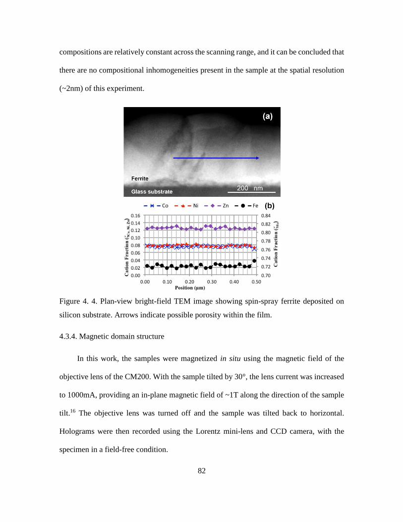
82
compositions are relatively constant across the scanning range, and it can be concluded that
there are no compositional inhomogeneities present in the sample at the spatial resolution
(~2nm) of this experiment.
Figure 4. 4. Plan-view bright-field TEM image showing spin-spray ferrite deposited on
silicon substrate. Arrows indicate possible porosity within the film.
4.3.4. Magnetic domain structure
In this work, the samples were magnetized in situ using the magnetic field of the
objective lens of the CM200. With the sample tilted by 30°, the lens current was increased
to 1000mA, providing an in-plane magnetic field of ~1T along the direction of the sample
tilt.16 The objective lens was turned off and the sample was tilted back to horizontal.
Holograms were then recorded using the Lorentz mini-lens and CCD camera, with the
specimen in a field-free condition.

83
The procedure of generating and interpreting the phase map are already described in
previous chapter. Also, as mentioned above, the phase map contains not only the magnetic
contribution to the phase but also contributions from diffraction and mean inner potential
of the sample.15 Although the uniform chemical composition shown in Fig. 4.4 indicates a
uniform mean inner potential, the phase shift due to diffraction still varies across the field
of view and adds difficulty to interpretation of the phase map.17 To eliminate this effect of
the inner potential, one hologram was recorded using the procedure described above. The
sample was removed from the microscope and flipped over, and another hologram was
then recorded from exactly the same area. Thus, two phase maps are generated, containing
the same phase contributions from the mean inner potential but with opposite magnetic
contributions. Thus the mean inner potential contributions to the phase can be removed by
subtracting the two images using suitable processing.
Figure 4.5 shows an example of this procedure applied to a plan-view sample. The
area observed was first recorded using the Lorentz lens, as shown in Fig. 4.5(a). This image
has limited magnification but this is still adequate to reveal the columnar structure as well
as showing some diffraction contrast. In order to reveal the crystal domain boundary more
clearly, the imaging was set to a slightly over-focus condition. The inserted black arrow
indicates the direction of the magnetizing field. Figure. 4.5(b) was then obtained from two
reconstructed phase images using the subtraction procedure outlined in the paragraph
above. The superimposed contour lines correspond to lines of constant phase. No phase
information is contained in the noisy areas at the top right and bottom left which were
outside the electron interference overlap area in the holograms. Figure 4.5(c) shows the
phase-gradient map obtained from Fig. 4.5(b), which can be interpreted as a magnetic
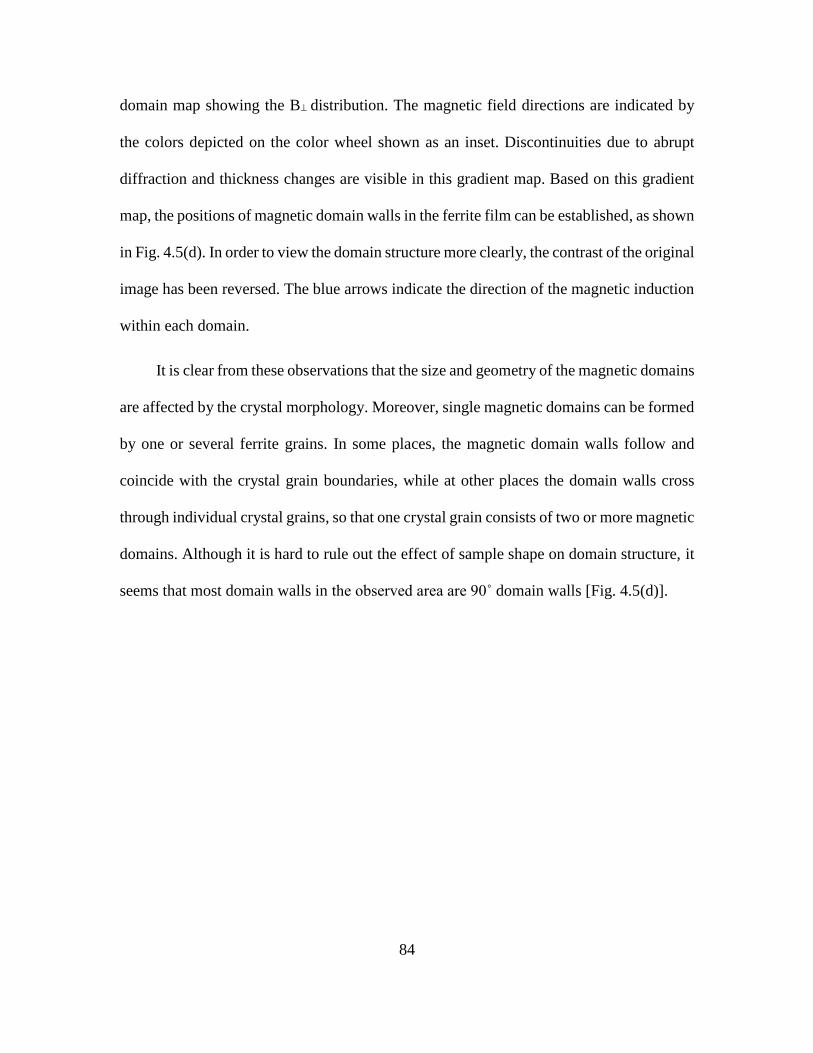
84
domain map showing the B⊥ distribution. The magnetic field directions are indicated by
the colors depicted on the color wheel shown as an inset. Discontinuities due to abrupt
diffraction and thickness changes are visible in this gradient map. Based on this gradient
map, the positions of magnetic domain walls in the ferrite film can be established, as shown
in Fig. 4.5(d). In order to view the domain structure more clearly, the contrast of the original
image has been reversed. The blue arrows indicate the direction of the magnetic induction
within each domain.
It is clear from these observations that the size and geometry of the magnetic domains
are affected by the crystal morphology. Moreover, single magnetic domains can be formed
by one or several ferrite grains. In some places, the magnetic domain walls follow and
coincide with the crystal grain boundaries, while at other places the domain walls cross
through individual crystal grains, so that one crystal grain consists of two or more magnetic
domains. Although it is hard to rule out the effect of sample shape on domain structure, it
seems that most domain walls in the observed area are 90˚ domain walls [Fig. 4.5(d)].

85
Figure 4. 5. (a) Plan-view image recorded using Lorentz mini-lens. (b) Reconstructed phase
map in plan-view obtained by subtracting two electron holograms to eliminate contribution
from mean inner potential. (c) Magnetic domain map. Inserted color wheel indicates the
relation between color wheel indicates the relation between color and magnetic induction
direction. (d) Contrast-reversed Lorentz image of (a) with magnetic domains indicated.

86
It is difficult to construct a model to calculate the sizes of the magnetic domains
because the film is not uniform, but the domain sizes can be directly determined. Some
grains give strong diffraction contrast in plan-view images which indicates that the
orientation is different. However, it is apparent that these grains can also form magnetic
domains together with neighboring grains having different crystal orientations. After close
examination of high-resolution TEM images of the grain (column) boundary regions, some
crystallized areas are found (Fig. 4.6). Such areas could provide a path for magnetization
links between neighboring grains to form single magnetic domains, which would lead to
this multiple-grain magnetic domain structure.
Figure 4. 6. High-resolution cross-section TEM image of grain boundary region showing
presence of crystal lattice fringes.
In addition to determining the magnetic domain structure of these ferrite films in the
remnant state, it is relevant to their potential applications to study domain wall motion or

87
rotation during the magnetization process. Using off-axis holography, it is possible to
follow the magnetization status during complete hysteresis loop cycling of magnetic
nanostructures.18 However, phase maps of these ferrite films often include very
complicated diffraction contrast features which make it difficult to fully interpret the
embedded magnetic information. Here, we only analyze phase gradient maps recorded at
remanence after saturation, as shown in Fig. 4.7. Figure 4.7(a) shows the phase gradient
map of a remnant state. The magnetization process around a complete hysteresis loop was
then performed on the sample. The phase gradient map of the new remnant state was
recorded in Fig. 4.7(b). Although the phase contributed by sample thickness is also
included in Figs. 4.7(a) and (b) and contributes to the phase gradient, this portion of the
phase gradient should be the same in both maps. Thus, the clearly visible differences of the
phase gradient distribution between these two maps is caused only by the magnetic
contribution, indicating that the magnetic domain morphology is not identical for the two
remnant states. This result demonstrates that the domain walls did not return to identical
positions when the sample was returned to the remnant state. Although it is unclear whether
the domain walls rotate or move during our magnetization experiments, the result indicate
that there are no preferred magnetization distributions in these ferrite films. Domain wall
rotation in this type of ferrite has been observed previously using Lorentz microscopy and
under-focus imaging.4 In that work, the applied magnetic field was small (maximum of
130Oe) and far below saturation. The porosity observed in Fig. 4.3 which also appears in
the ferrite film in Ref. 3 might support the notion of domain-wall pinning.

88
Figure 4. 7. (a) and (b) Reconstructed phase maps in plan-view geometry recorded at
saturated remanence states before and after magnetization following a complete hysteresis
loop. (c) Phase map obtained by subtracting (a) from (b).
The holography observations provide information about the in-plane magnetic
domain structure of the ferrite films. To check for possible out-of-plane magnetic
components, AFM/MFM measurements were also made. However, MFM usually requires
a relatively smooth surface, but some chemical residue often attaches to the surface and
cannot be removed by regular cleaning. Moreover, SEM imaging (not shown here) also
indicated that the surface of the spin-spray ferrite might be too rough for this type of
measurement. Cloth polishing plate and artificial diamond solution with average size of

89
40nm were thus used to smooth the surface. The AFM and MFM results after polishing are
shown in Fig. 4.8. Some features are visible in the MFM scan [Fig. 4.8(a)] but these are
almost certainly caused by the surface morphology since corresponding features are also
visible at the same locations in AFM images [Fig. 4.8(b)]. Moreover, no features
resembling magnetic domains are obviously visible in MFM scans. Finally, off-axis
electron holography was done on several cross-section samples. The reconstructed phase
maps (not shown here) showed no evidence of any magnetic fields extending outside the
sample. Thus, it can be concluded that the magnetization of the ferrite films must be
restricted to in-plane.
Figure 4. 8. MFM (a), and AFM (b), images from polished surface of ferrite sample.
4.4 Conclusions
Electron holography and high resolution imaging of the magnetic domain and
physical grain structures in nanocrystalline nickel-zinc-cobalt ferrite films revealed that
magnetic domains could span across several grains. These observations were conducted on

90
~250nm-thick films that were grown by aqueous spray deposition onto silicon and glass
substrates. Characteristically, the grain microstructures of the films were columnar,
comprising of ~100nm diameter grains with their long axes oriented perpendicular to the
substrate plane. Off-axis electron holography of the films in plan-view provided direct
evidence that magnetic domains were formed by multiple crystal grains. The magnetic
domains were somewhat irregular in shape, with domain walls often following the
crystalline grain boundaries, but in some cases crossing through individual grains. Abrupt
disruptions in crystal orientation at grain boundaries did not necessarily cause disruption
in the orientation of the magnetic domains. Because electron holography is a technique that
senses magnetic fields in directions perpendicular to the electron beam, magnetic force
microscopic imaging was also carried out on the same material, again in plan-view. The
latter results revealed no net magnetic structure perpendicular to the film plane and parallel
to the columnar grains, indicating that the internal magnetic fields were oriented in-plane
only.

91
References
1N. Ray, “Synthesis and Characterization of Nanocrystalline Nickel-Zinc Spinel Ferrite
Thin Films Using the Spin-Spray Deposition Method.” UMI Proquest, Arizona State
University. PhD (2013): 140.
2D. Zhang, N. M. Ray, W. T. Petuskey, D. J. Smith and M. R. McCartney, J. Appl. Phys.
116, 083901 (2014).
3A. Goldman, Modern Ferrite Technology, 2nd Ed (Springer, Pittsburgh, 2006) p.273.
4H. Yoshikawa, K. Kondo, S. Yoshida, D. Shindo and M. Abe, IEEJ Trans. 2, 445-449
(2007).
5N. Matsushita, C. P. Chong, T. Mizutani and M. Abe. J. App. Phys. 91, 10 (2002).
6D. Jiles, Introduction to Magnetism and Magnetic Materials, 2nd Ed (Taylor & Francis,
New York, 1998).
7Y. Tamaura, M. Abe, Y. Goto, N. Kitamura, and M. Gomi, J. Appl. Phys. 61, 3211
(1987).
8N. Matsushita, C. Chong, T. Mizutani and M. Abe, IEEE Trans. Magn. 38, 5 (2002).
9T. Sebastian, S. A. Clavijo, and R. E. Diaz, J. Appl. Phys. 113, 033906 (2013).
10K. Kondo, S, Yoshida, H, Ono and M. Abe, J. Appl. Phys. 101, 09M502 (2007).
11K. Kondo, T. Chiba, H. Ono, S. Yoshida, Y. Shimada, N. Matsushita and M. Abe, J.
Appl. Phys. 93, 10 (2003).
12M. Abe, T. Itoh and Y. Tamaura, Thin Solid Film. 216, 155 (1992).
13A. K. Subramani, K. Kondo, M. Tada, M. Abe, M. Yoshimura and N. Matsushita,
Mater. Chem. Phys. 123, 16-19 (2010).
14N. Matsushita, T. Nakamura and M. Abe, J. Appl. Phys. 93, 10 (2003).
15N. Matsushita, T. Nakamura, and M. Abe, Proc. 2002 IEEE Int. Magn. Conf.
Amsterdam, Netherland, April 28-May 2, 2002.
16R. E. Dunin-Borkowski, M. R. McCartney, B. Kardynal, S. S. P. Parkin, M. R.
Scheinfein and D. J. Smith, J. Microsc. 200, 187-205 (2000).

92
17R. E. Dunin-Borkowski, M. R. McCartney, D. J. Smith, and S. S. P. Parkin,
Ultramicroscopy. 74, 61 (1998).
18H. Hu, H. Wang, M. R. McCartney and D. J. Smith, J. Appl. Phys. 97, 054305 (2005).

93
CHAPTER 5
PERPENDICULAR MAGNETIC ANISOTROPY AND MAGNETIC DOMAINS IN
CoFe/Pd MULTILAYERS
Multilayers of Co90Fe10/Pd with different bilayer thicknesses, have been deposited
by dc-magnetron sputtering on thermally oxidized Si wafers. Transmission electron
microscopy showed that the highly textured crystalline films had columnar structure, while
scanning transmission electron microscopy and atomic force microscopy respectively
indicated some layer waviness and surface roughness. The magnetic domain structure and
perpendicular magnetic anisotropy (PMA) of the Co90Fe10/Pd multilayers were
investigated by off-axis electron holography and magnetic force microscopy. The Co90Fe10
layer thickness was the primary factor determining the magnetic domain size and the
perpendicular magnetization: both decreased as the thickness increased. The strongest
PMA was observed in the sample with the thinnest magnetic layer of 0.45 nm. The samples
investigated here were grown by Dr. Justin Shaw of National Institute of Science and
Technology, and the major results have been submitted for publication.1
5.1 Introduction
Magnetic thin films and nanostructures that are magnetized perpendicular to their
surface are essential to many developing technologies, including spintronics devices2 and
patterned media,3-4 especially because of the need to maintain thermal stability as device
dimensions are reduced deeper into the nanoscale. Multilayers or superlattice structures
consisting of alternating ferromagnetic and nonmagnetic layers are highly suitable for these

94
applications due to their tunable perpendicular magnetic anisotropy (PMA) and saturation
magnetization.5-7 The magnetic microstructure is crucial for developing potential devices,
and such multilayered structures have been extensively studied using different
characterization techniques.8-14 For example, magnetic force microscopy (MFM) applied
to samples consisting of Co/Pd multilayers showed striped domain structure,10-11 and X-
ray magnetic circular dichroism (XMCD) revealed changes in the domain structure in
different layers of NiFe/Au/Co/Au multilayers.12 Magnetic optical Kerr (MOKE)
microscopy has also been used to reveal magnetic domain formation and switching
behavior,13 and it was reported that PMA was present in amorphous CoSiB/Pt multilayers
that had similar striped domains.14 In this present work, off-axis electron holography has
been used to investigate the PMA and magnetic domain structure of Co90Fe10/Pd
multilayers of different layer thicknesses. Transmission electron microscopy (TEM), and
high-angle annular-dark-field (HAADF) scanning transmission electron microscopy
(STEM) were used to determine the microstructure, and atomic force microscopy (AFM)
together with magnetic force microscopy (MFM) were used to compare the surface
morphology and domain structure of the films.
5.2 Experimental details
The multilayer system consisted of Co90Fe10/Pd multilayers with the basic structure of
Ta/Pd/[Co90Fe10/Pd] 12/Pd, where the thicknesses of the magnetic layers were tCoFe = 0.45
nm, 0.8 nm or 1 nm, and the ratio of thicknesses between the Co90Fe10 and Pd layers was
kept fixed at 1 : 2. All samples were prepared at room temperature by dc magnetron sputter
deposition at an Ar pressure of ~ 66 mPa (0.5 mTorr) onto oxidized Si(001) substrates.
Deposition rates were calibrated using x-ray reflectivity (XRR), which indicated a

95
maximum drift in deposition rates of 3% throughout the study. All samples contained 3-
nm Ta / 3-nm Pd seed layers, and a final 3-nm Pd capping layer was also used to prevent
oxidation.
Samples suitable for cross-sectional (S)TEM observations were prepared by cleaving
and mechanical wedge-polishing, followed by 2.5-keV Ar-ion-milling at liquid-nitrogen
temperature to create electron-transparent areas. TEM and STEM images were recorded
using a JEOL JEM-2010F† equipped with a thermal-field-emission electron gun operated
at 200 keV. Off-axis electron holography studies were performed using a Philips-FEI
CM200 FEG TEM operated at 200 keV and an FEI Titan 80-300 ETEM operated at 300
keV. The latter two microscopes were each equipped with an electrostatic biprism and a
small (Lorentz) mini-lens located below the lower pole piece of the objective lens, enabling
the samples to be studied in field-free conditions. A positive biprism voltage of ~100 V,
corresponding to an interference-fringe spacing of ~2 nm, was typically used to record
electron holograms in the Lorentz imaging mode using a CCD camera. In the field-free
imaging condition, the presence of PMA was revealed by magnetization perpendicular to
the plane of the multilayer interfaces. To confirm the magnetic easy axis of the multilayers,
all TEM samples were also magnetized in situ using magnetic fields of close to 2 T, with
the direction of the applied field parallel to the multilayer interfaces (i.e. in the film plane).
This external magnetic field was created using the objective lens of the microscope and
was removed before the holograms were recorded.

96
5.3 Results and discussion
5.3.1 Surface morphology
AFM was used to check the sample surfaces after deposition, and results for the three
samples are shown in the left column of Fig. 5.1. Granular surface features were visible for
all samples with the sizes of these features increasing for larger tCoFe. Statistical analysis of
the images indicated that the average grain sizes of the samples were 23 nm, 26 nm and 29
nm for tCoFe = 0.45 nm, 0.8 nm and 1 nm, respectively. MFM scans to reveal out-of-plane
magnetic domain structure were also made after applying in-plane magnetic fields of 1.1
T, and the corresponding results for each sample are shown at the right side of each AFM
image. By comparing images for tCoFe = 0.45nm and 0.8nm, it is clear that increasing tCoFe
changes the magnetic domain structure and decreases the domain size. A striped domain
structure in Fig. 5.1 (e) is apparent for tCoFe = 0.8nm but no out-of-plane domain structure
is visible in Fig. 5.1 (f), corresponding to the sample with tCoFe = 1 nm.

97
Figure 5. 1. AFM images (left), and corresponding MFM images (right), from the CoFe/Pd
multilayer surfaces. Scale bar for AFM images = 1 μm, for MFM images = 200 nm.

98
5.3.2 Crystalline structure
Figure 5.2 (a) is a bright-field TEM image showing a cross section of the Co90Fe10/Pd
multilayers for the sample with tCoFe = 0.8 nm. In this diffraction-contrast image, the
separate Co90Fe10 alloy and Pd layers are visible as roughly horizontal regions of lighter
and darker contrast, respectively. However, the contrast within each layer is not uniform,
indicating that the multilayers are not well defined and/or have considerable thickness
variation and polycrystallinity. Moreover, the image contrast in the direction perpendicular
to the substrate surface indicates that the film has a columnar morphology, which causes
some surface roughness. As indicated in Fig. 5.2 (a), these columns and surface bumps
have dimensions that roughly correspond to the average width of the granular features
visible in AFM scans such as Fig. 5.1 (b). High-resolution phase-contrast images, such as
Fig. 5.2 (b), indicate that the columns are crystalline with pronounced in-plane texture. A
narrow region with dark contrast, corresponding to the Ta and Pd seed layers, is visible
between the SiOx and metal multilayers. This layer can be observed more clearly in the
enlargement inserted in Fig. 5.2 (b), and shows some slight signs of crystallinity. The
samples with larger tCoFe had reduced layer waviness and surface roughness relative to the
sample with tCoFe = 0.45 nm.

99
Figure 5. 2. (a) Cross-section TEM image of CoFe/Pd multilayer sample with tCoFe = 0.8
nm showing columnar morphology; (b) HRTEM image showing bottom part of multilayer
for tCoFe = 0.8 nm showing textured crystal grains with random in-plane orientations.
Enlargement shows layer just above SiOx.
The waviness of the layers is more apparent using STEM HAADF imaging since the
image contrast in this mode is highly dependent on atomic number. Figures 5.3 (a) and (b)
compare HAADF images from the samples with tCoFe = 0.45 nm and 1 nm, respectively.
The multilayer structure is clearly visible, and the thicknesses of the layers are consistent
with the nominal values. The multilayers become increasingly wavy away from the
substrate and the interfaces seem to be less well defined, while the sample with tCoFe = 0.45

100
nm shows greater relative waviness than the sample with tCoFe = 1 nm. Line profiles of
image intensity are shown in Figs. 5.3 (c) and (d). Following the deconvolution method for
determining compositional variations used by Crozier and colleagues,15-16 intensity
simulations were carried out, and these are shown as inserted bold lines in Figs. 5.3 (c) and
(d). In these simulations, the nominal elemental compositions and profiles of the
Co90Fe10/Pd superlattices were used. The differences between the experimental and
simulated profiles indicate that some interdiffusion has occurred at the interfaces. Since all
samples were grown under the same conditions, this interdiffusion will have a relatively
greater effect on samples with smaller layer thicknesses.
Figure 5. 3. Cross-section HAADF images of CoFe/Pd multilayer samples with (a) tCoFe =
0.45 nm, and (b) tCoFe = 1 nm. (c) & (d) Line profiles of the intensity positions and
directions as indicated by red arrows in (a) & (b). Simulated intensity profiles are inserted
as bold lines.

101
5.3.3 Magnetic domain structure
Off-axis electron holography is an interferometric electron–microscope technique that
provides quantitative access to phase shifts experienced by the incident electron wavefront
due to interactions with the electrostatic and magnetic potentials of the sample.17 The
changes in phase of the electron wave deduced from an electron hologram can then be used
to provide quantitative information about the magnetic fields within and outside the sample
with a spatial resolution that can approach the nanometer scale under optimal conditions.18-
19 Figure 5.4 (a) shows a typical example of a reconstructed phase map from the sample
with tCoFe = 0.45 nm, where the magnitude of the local phase change is represented by
changes in color. No clear information is available from within the multilayer region
(labelled ML) because of phase-wrapping issues.19 However, two magnetic domains are
clearly visible in the amplified (8) phase image in Fig. 5.4 (b), showing magnetization
perpendicular to the sample surface. Line profiles of the phase were made in the vacuum
region near the top surfaces of the multilayers, and on the silicon oxide film near the bottom
of the multilayers, as indicated by the dotted lines in Fig. 5.4 (a). These phase profiles are
shown in Figs. 5.4 (c) and (d). The positions of magnetic domain walls can be identified
from these line profiles, as indicated by the arrows. The magnitude of the magnetic field in
projection related to the magnetic domains can also be estimated. Moreover, it can be seen
that the magnetic fields emerging from the top and bottom surfaces of the multilayers are
basically identical. Further observations of the samples with larger tCoFe revealed similar
magnetic domain structure, except that these multilayers generated weaker magnetic field
perpendicular to the sample surface. Perpendicular magnetic field was revealed by
holography for the sample with tCoFe = 1 nm but not apparent in the MFM images. In

102
addition to the enhanced detection limit of holography compared with MFM,20 it is also
possible that additional shape anisotropy resulting from cross-sectioning of the continuous
film caused partial reorientation of the in-plane magnetization of the continuous film to the
perpendicular direction.
Figure 5. 4. (a) Reconstructed holography phase map of multilayers with tCoFe = 0.45 nm,
(b) Amplified (8) phase image showing distribution of magnetic domains. (c) and (d) Line
profiles from positions 1 and 2, respectively, marked in (a) by white arrows.
These holography experiments were done on cross-sectional TEM samples, so it might
be anticipated that the revealed magnetic domain structure could be affected by the
lamellar-like sample geometry. Indeed, our observation revealed that the apparent sizes of
the magnetic domains changed slightly with the projected sample thickness along the
electron-beam direction. The magnetic domain structures observed in phase maps, such as
Fig. 5.4, are different from the structures observed by MFM, as shown in Fig. 5.1. Thus,

103
the TEM sample geometry has some effect on the apparent magnetic domain size because
the domains are constrained by the shorter plane of the multilayers rather than being
randomly distributed. Figure 5.5 shows reconstructed phase maps for the sample with tCoFe
= 0.8 nm indicating slight changes in the magnetic domain structure from areas with
different projected sample thicknesses. The thickness values were estimated using the
reconstructed amplitude image and the known inelastic-mean-free-path of silicon (±10%
error estimate).21-22 The magnetic domains have average widths of 116 nm, 120 nm and
130 nm for areas with projected thicknesses of 412 nm, 525 nm and 729 nm. In addition to
the effect on magnetic domain structure, sample cross-sectioning will affect how much
fringing field could be included in an electron projection. To compare the PMA between
samples with different tCoFe, phase maps were generated from areas with similar local
thickness for each sample. Since the effect of tCoFe on PMA was already well studied using
MFM, such as shown as Fig. 5.1, the holography results comparing PMA are omitted here.

104
Figure 5. 5. Phase maps for CoFe/Pd multilayer sample with tCoFe = 0.8 nm. Sample
thicknesses in beam direction are: (a) 412 nm, (b) 525 nm, (c) 729 nm. Scale bar = 100 nm
in each case.
Figure 5.6 (a) shows another example of a phase map in the vacuum near the top
surface of the sample with tCoFe = 0.45 nm. Contour lines corresponding to two magnetic
domains are visible in the phase-amplified map shown in Fig. 5.6 (b). These contour lines
indicate differences in magnetic domain size, which could be caused either by different
values of the magnetic field in projection or by rotation of the magnetic domains. In
comparison, for the sample with tCoFe = 0.8 nm, as shown in Fig. 5.6 (c) and (d), contour
lines generated from different magnetic domains showed almost the same morphology,
indicating less variability. Considering that PMA has an orientation that follows the
multilayer stacking, layer waviness in the sample with thinner tCoFe is likely to cause
variation among magnetic domains. Studies carried out by ferromagnetic resonance (FMR)

105
also indicate that magnetic inhomogeneity increases as the anisotropy increases.23 This
result agrees with our observations because the PMA for these multilayers increases as tCoFe
decreases.
Figure 5. 6. (a) Phase map for CoFe/Pd multilayers sample with tCoFe = 0.45 nm. (b)
Modified (cos) phase image of (a) showing contour lines; (c) Phase map of multilayers
with tCoFe = 0.8 nm. (d) Modified (cos) phase image of (c) showing contour lines.
To further investigate the relationship between magnetic domain structure and
microstructure, the positions of magnetic domain walls were marked on Lorentz images
taken from the same areas where phase maps were generated. Although Lorentz images
have limited resolution and less intensity than conventional TEM images, columns with
different crystalline orientations are still visible. Figure 5.7 shows a Lorentz image from
the sample with tCoFe = 1 nm, with the positions of magnetic domain walls indicated. The
phase map used to locate these domains is also shown as an insert. As illustrated in Fig.
5.7, two magnetic domains with almost equal size are visible. In this case, there is no
apparent correlation between the positions of magnetic domain walls and columns,
although the crystal structure within the two areas covered by these two magnetic domains
seems different.

106
Figure 5. 7. Lorentz image for CoFe/Pd multilayers sample with tCoFe = 1 nm, magnetic
domain walls in imaging area are indicated by red arrows. Phase map used for locating
domain wall shown as insert.
5.4 Conclusions
Electron holography in conjunction with other characterization techniques has been
used to investigate the variation of domain structure and perpendicular magnetic anisotropy
in CoFe/Pd multilayers of different magnetic layer thickness (tCoFe) in the range of 0.45 nm
to 1.0 nm. All films showed a textured columnar morphology with some chemical
interdiffusion between layers. In addition, for smaller tCoFe, it was observed: i) The average
columnar width within the film decreased but not impact magnetic domain formation; ii)
Layer waviness and surface roughness increased; iii) More relative interdiffusion between
multilayers; iv) The magnetic domain size and the magnetic field originating from each
domain perpendicular to the sample surface increased; v) Variability between the magnetic
107
domains increased. Thus these results confirm that bilayer thickness is the predominant
factor affecting the magnetic domain structure and PMA. It is known that factors such as
surface roughness, structure inhomogeneity and interdiffusion caused by decreasing tCoFe
could deteriorate PMA,24-28 but this study confirmed that the sample with the thinnest CoFe
layer of 0.45 nm still showed the strongest PMA. Overall, these results indicate the
usefulness of off-axis electron holography as an alternative approach for characterizing the
domain structure and PMA of magnetic multilayers, although the possibility of changes
caused by sample cross-sectioning will still need to be taken into account.
108
References
1Desai Zhang, Justin M. Shaw, David J. Smith and Martha R. McCartney, J. Magn. Magn.
Mater. 388, 16 (2015).
2S. Mangin, D. Ravelosona, J. A. Katine, M. J. Carey, B. D. Terris and E. E. Fullerton,
Nature Mater. 5, 210-215 (2006).
3M. Todorovic, S. Schultz, J. Wong and A. Scherer, Appl. Phys. Lett. 74, 2516-2518
(1999).
4J. Ding and A. O. Adeyeye, Adv. Funct. Mater. 23, 1684-1691 (2013).
5C. T. Boone, Hans T. Nembach, Justin M. Shaw and T. J. Silva, J. Appl. Phys. 113,
153906 (2013).
6W. H. Rippard, A. M. Deac, M. R. Pufall, J. M. Shaw, M. W. Keller, Stephen E. Russek,
G. E. W. Bauerand and C. Serpico, Phys. Rev. B 81, 014426 (2010).
7B. D. Terris and T. Thomson, J. Phys. D 38, R199-R222 (2005).
8Y. Xiao, Z. Zhang, B. Ma, Q.Y. Jin and Y. Liu, Appl. Phys. Lett. 104, 072403 (2014).
9W. R. Bennett, C. D. England, D. C. Person and C. M. Falco, J. Appl. Phys. 69, 4384-
4390 (1990).
10R. Sbiaa, Z. Bilin, M. Ranjbar, H. K. Tan, S. J. Wong, S. N. Piramanayagam and T. C.
Chong, J. Appl. Phys. 107, 103901 (2010).
11M. S. Pierce, J. E. Davies, J. J. Turner, K. Chesnel, E. E. Fullerton, J. Nam, R.
Hailstone, S. D. Kevan, J. B. Kortright, Kai Liu, L. B. Sorensen, B. R. York and O.
Hellwig, Phys. Rev B 87, 184428 (2013).
12B. Szymanski, P. Mazalski, M. Urbaniak, F. Stobiecki, A. Maziewski, S. Pizzini and F.
Maccherozzi, IEEE Trans. Magn. 46, 231-234 (2010).
13G. Gubbiotti, G. Carlotti, S. Tacchi, M. Madami, T. Ono, T. Koyama, D. Chiba, F.
Casoli and M.G. Pini, Phys. Rev. B 86, 014401 (2012).
14Y. H. Choi, K. J. Lee, J. B. Yoon, J. H. Cho, C.-Y. You, T. W. Kim and M. H. Jung, J.
Appl. Phys. 115, 183901 (2014).
15P. A. Crozier, M. Catalano and R. Cingolani, Ultramicroscopy, 94, 1-13 (2003).
16P. A. Crozier, M. Catalano, R. Cingolani and A. Passaseo, Appl. Phys. Lett. 79, 3170-
3172 (2001).
109
17M. R. McCartney and D. J. Smith, Annu. Rev. Mater. Res. 37, 729-767 (2007).
18R. E. Dunin-Borkowski, M. R. McCartney, D. J. Smith and S. S. P. Parkin,
Ultramicroscopy 74, 61-73 (1998).
19H. Lichte, P. Formanek, A. Lenk, M. Linck, C. Matzeck, M. Lehmann and P. Simon,
Annu. Rev. Mater. Res. 37, 539-588 (2007).
20H. Lichte, Ultramicroscopy 108, 256-262 (2008).
21T. M. Chou and M. Libera, Ultramicroscopy 94, 31-35 (2003).
22M. R. McCartney and M. Gajdardziska-Josifovska, Ultramicroscopy 53, 283-289
(1994).
23J. M. Shaw, H. T. Nembach and T. J. Silva, Phys. Rev. B 85, 054412 (2012).
24J. M. Shaw, H. T. Nembach, T. J. Silva, S. E. Russek, R. Geiss, C. Jones, N. Clark, T.
Leo and D. J. Smith, Phys. Rev. B 80, 184419 (2009).
25J. M. Shaw, H. T. Nembach, and T. J. Silva, J. Appl. Phys. 108, 093922 (2010)
26Y. Zhu, Z. Zhang, B. Ma and Q. Y. Jin, J. Appl. Phys. 111 07C106 (2012).
27M. Gottwald, K. Lee, J. J. Kan, B. Ocker, J. Wrona, S. Tibus, J. Langer, S. H. Kang and
E. E. Fullerton, Appl. Phys. Lett. 102, 052405 (2013).
28S. Bandiera, R. C. Sousa, B. Rodmacq and B. Dieny, Appl. Phys. Lett. 100, 142410
(2012).
110
CHAPTER 6
SUMMARY AND POSSIBLE FUTURE WORK
6.1 Summary
This dissertation has described applications of off-axis electron holography to
characterizing different types of magnetic nanostructures, both qualitatively and
quantitatively. Representative examples, including Co nanoparticles (NPs), core/shell
magnetic nanowires (NWs), carbon spirals with magnetic core and magnetic nanopillars
were studied using electron holography and Lorentz microscopy. The observations of Co
NP chains involved interpreting magnetic induction based on phase information provided
by reconstructed holograms. The cobalt oxide shell, the multigrain structure and the
demagnetizing field had to be considered when determining the magnetic induction. The
GaAs/Fe/Au core/shell NWs grown on GaAs (111)B substrates had cylindrical shells with
magnetic fields confined within the shells and forming closed loops. On the other hand,
NWs grown on (110) substrate with rotationally non-uniform Fe coating formed magnetic
induction patterns similar to a bar magnet, although on different length scales.1 Holography
experiments using a heating holder combined with EELS confirmed that iron was
responsible for the observed magnetism even though it could not be revealed directly using
high-resolution imaging. Studies of the carbon spirals showed that the iron cores had
formed multi-magnetic-domains and the magnetic field only extended over a limited range.
Finally, it was disappointing that no magnetism was successfully revealed from CoPdFe
nanopillars under different imaging conditions.
The magnetic domain structure present in thin films of nanocrystalline Ni-Zn-Co
spinel ferrite synthesized using aqueous spin-spray coating was characterized in detail.2

111
After subtraction of the phase contribution from the mean inner potential, phase maps in
plan-view provided direct evidence that magnetic domains consisting of multiple crystal
grains were formed. The magnetic domain walls often followed crystalline grain
boundaries but, in many cases, also crossed through individual grains. Observations of
remnant states indicated that there was no preferred magnetization distribution in these
films. Moreover, the magnetization of the ferrite films was shown to be restricted to in-
plane.
The magnetic domain structure and perpendicular magnetic anisotropy (PMA) in
CoFe/Pd multilayers of different magnetic layer (CoFe) thickness were studied using
electron holography in conjunction with other electron microscopy techniques.3 TEM and
STEM observations indicated that all films had columnar morphology but with some
chemical interdiffusion between layers. After carefully evaluating the effect of sample
cross-sectioning, electron holography confirmed that magnetic layer thickness was the
predominant factor affecting the PMA and the magnetic domain structure. Even the
columnar structure itself had little impact on the magnetic domain formation. Although
decreasing the magnetic layer thickness always caused surface roughness, interdiffusion
and some structure inhomogeneity, which are considered to be factors that can deteriorate
PMA, the sample with the thinnest CoFe layer still showed the strongest PMA. Moreover,
phase contours showed that the variability between magnetic domains increased as the
magnetic layer thickness decreased.
Overall, off-axis electron holography was confirmed from these studies to be a unique
and powerful technique able to provide visualization and quantification of magnetic
materials with nano-scale spatial resolution. As a technique based on transmission electron

112
microscopy, holography should provide more opportunities for physics and materials
research, especially with the development of modern state-of-the-art microscopes which
offer the very real prospect of sub-nanometer-scale resolution for studying magnetic
materials.
6.2 Future work: Skyrmions
6.2.1 Introduction
Skyrmions represent topologically stable field configurations with particle-like
properties.4 As a kind of nanoscale spin texture, Skyrmions are viewed as promising
candidates for information carriers in future spintronics devices.5-7 From the viewpoint of
fundamental science, Skyrmions have been described by general concepts in physics
ranging from elementary particles to liquid crystals, Bose-Einstein condensates and
quantum Hall magnets, and show similarities to the vortex lattice in type II
superconductors.8 Temperature-magnetic field phase diagrams have been developed for
studying Skyrmion formation, as shown in Fig. 6.1.9
Figure 6. 1. Magnetic phase diagram under H || [111], deduced for (A) bulk and (B) thin-
film forms of Cu2OSeO3, respectively.9
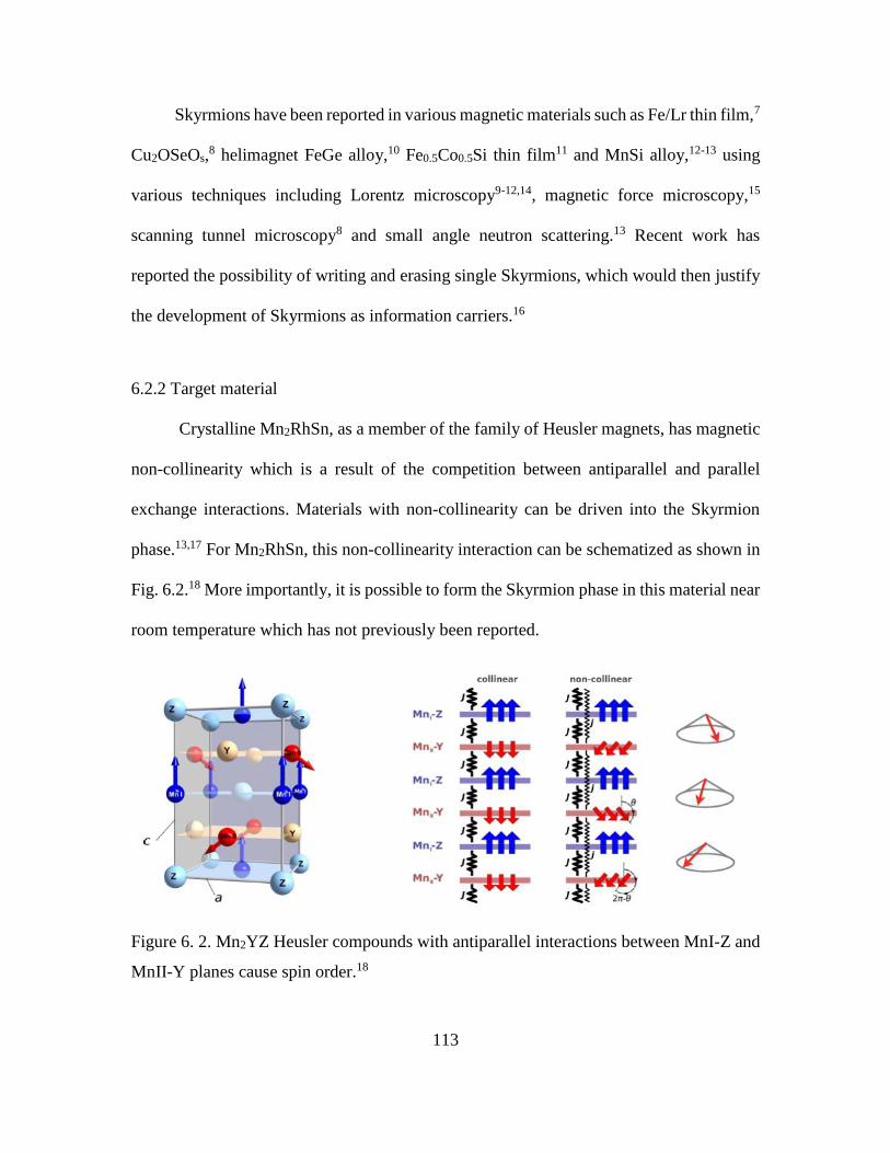
113
Skyrmions have been reported in various magnetic materials such as Fe/Lr thin film,7
Cu2OSeOs,8 helimagnet FeGe alloy,10 Fe0.5Co0.5Si thin film11 and MnSi alloy,12-13 using
various techniques including Lorentz microscopy9-12,14, magnetic force microscopy,15
scanning tunnel microscopy8 and small angle neutron scattering.13 Recent work has
reported the possibility of writing and erasing single Skyrmions, which would then justify
the development of Skyrmions as information carriers.16
6.2.2 Target material
Crystalline Mn2RhSn, as a member of the family of Heusler magnets, has magnetic
non-collinearity which is a result of the competition between antiparallel and parallel
exchange interactions. Materials with non-collinearity can be driven into the Skyrmion
phase.13,17 For Mn2RhSn, this non-collinearity interaction can be schematized as shown in
Fig. 6.2.18 More importantly, it is possible to form the Skyrmion phase in this material near
room temperature which has not previously been reported.
Figure 6. 2. Mn2YZ Heusler compounds with antiparallel interactions between MnI-Z and
MnII-Y planes cause spin order.18

114
6.2.3 Revealing Skyrmions using off-axis electron holography
Similar to the experiments described in previous chapters, off-axis electron
holography could be applied to characterize Skyrmions. Using nano-scale spatial
resolution, quantitative information about the Skyrmions could be provided by the
development of suitable phase maps.
Experimental difficulties still require more effort. First, Skyrmion formation depends
on crystal orientation.13 To reveal possible Skyrmions using holography, the TEM samples
must be prepared in preferred crystalline orientations to ensure that the electron beam
penetrating the sample is parallel or perpendicular to the ‘c’ axis, as shown in Fig. 6.2. The
starting material is normally the bulk alloy, synthesized using arc-melting, and it is
supposed to be polycrystalline, which will make it difficult to locate any desired orientation.
Figure 6.3 shows a region of polycrystalline FeGe film grown on Si, which is a candidate
material for Skyrmion formation. Although one or two grains are in preferred orientation,
the multigrain structure visible here will result in complicated diffraction contrast which
makes this particular sample inherently unsuitable for Skyrmions searching. A similar
problem may also occur for Mn2RhSn alloys.
The estimated diameter of Skyrmions in this material is around 50 nm.10,18
Quantitative phase characterization on such illusive configurations demands high signal to
noise ratio because the phase change caused by them might be very weak. Besides pushing
the imaging condition of electron holography to optimal limit, the effect of static electricity
charging will need to be overcome.

115
Figure 6. 3. Bright-field plan-view TEM image of FeGe film grown on silicon.
Figure 6.4 shows a cross-section TEM image of the Co/Ni/Co/Ru/Co/Ni/Co film
provided by the group of Dr. Stuart Parkin at IBM Almaden Research Center. It is expected
that Skyrmions should be present in this film with rotation axis perpendicular to the
substrate. However, the aluminum oxide beneath the film, caused strong static electricity
which generated an overlapping phase signal that swamped the possible Skymion signal.
This situation is illustrated in Fig. 6.5, which is a phase map of this material generated in
plan-view geometry. The giant rainbow in the phase map looks like a textbook example of
static electricity charging, leaving no possibility for finding electron spin texture. To
resolve this problem, charge-cancelling processing such as thin-metal-film coating or
environmental gas neutralizing need to be attempted.

116
Figure 6. 4. Cross-section TEM image of Co/Ni/Co/Ru/Co/Ni/Co film, which is a
possible candidate for Skyrmion observation using electron holography.
Figure 6. 5. Phase map of Co/Ni/Co/Ru/Co/Ni/Co film in plan-view geometry.

117
References
1R. E. Pimpinella, D. Zhang, M. R. McCartney, D. J. Smith, K. L. Krycka, B. J. Kirby, B.
J. O'Dowd, L. Sonderhouse, J. Leiner, X. Liu,M. Dobrowolska and J. K. Furdyna, J.
Appl. Phys. 113, 17B520 (2013).
2D. Zhang, N. M. Ray, W. T. Petuskey, D. J. Smith and M. R. McCartney, J. Appl. Phys.
116, 083901 (2014).
3Desai Zhang, Justin M. Shaw, David J. Smith and Martha R. McCartney, J. Magn. Magn.
Mater. 388, 16 (2015).
4N. Nagaosa and Y. Tokura, Nature Nanotech. 8, 899 (2013).
5A. Fert, V. Cros and J. Sampaio, Nature Nanotech. 8, 152–156 (2013).
6Iwasaki, J., Mochizuki, M. & Nagaosa, N. Nature Commun. 4, 1463 (2013).
7A. Rosch, Nature Nanotech. 8,160–161 (2013).
8S. Heinze, K. von Bergmann, M. Menzel, J. Brede, A. Kubetzka, R. Wiesendanger, G.
Bihlmayer and S, Blügel, Nature Phys. 7, 713-718 (2011).
9S. Seki, X. Yu, S. Ishiwata and Y. Tokura, Science 336, 198 (2012).
10X. Yu, N. Kanazawa, Y. Onose, K. Kimoto, W. Z. Zhang, S. Ishiwata, Y. Matsui and
Y. Tokura, Nature Materials 10, 106-109 (2011).
11H. Park, X. Yu, S. Aizawa, T. Tanigaki, T. Akashi, Y. Takahashi, T. Matsuda, N.
Kanazawa, Y. Onose, D. Shindo, A. Tonomura and Y. Tokura, Nat. Nanotechnol. 9, 337-
342 (2014).
12A. Tonomura, X. Yu, K. Yanagisawa, T. Matsuda, Y. Onose, N. Kanazawa, H. Park,
and Y. Tokura, Nano Lett. 12, 1673−1677 (2012).
13S. Mühlbauer, B. Binz, F. Jonietz, C. Pfleiderer, A. Rosch, A. Neubauer, R. Georgii and
P. Böni, Science 323, 915 (2009).
14X. Yu, Y. Onose, N. Kanazawa, J. H. Park, J. Han, Y. Matsui, N. Nagaosa and Y.
Tokura, Nature 465, 901-904 (2010).
15P. Milde, D. Köhler, J. Seidel, L. Eng, A. Bauer, A. Chacon, J. Kindervater, S.
Mühlbauer, C. Pfleiderer, S. Buhrandt, C. Schütte and A. Rosch, Science 340, 1076
(2013).
118
16N, Romming, C. Hanneken, M. Menzel, J. Bickel, B. Wolter, K. von Bergmann, A.
Kubetzka and R, Wiesendanger, Science 341, 6146 (2013).
17F. Jonietz, S. Mühlbauer, C. Pfleiderer, A. Neubauer, W. Münzer, A. Bauer, T. Adams,
R. Georgii, P. Böni, R. A. Düine, K. Everschor, M. Garst and A. Rosch, Science 330,
1648 (2010).
18O. Meshcheriakova, S. Chadov, A. K. Nayak, U. K. Rößler, J. Kübler, G. André, A. A.
Tsirlin, J. Kiss, S. Hausdorf, A. Kalache, W. Schnelle, M. Nicklas, and C. Felser, Phys.
Rev. Lett. 113, 087203 (2014).
119
References
A. Akhtari-Zavareh, L. P. Carignan, A. Yelon, D. Ménard, T. Kasama, R. Herring, R. E.
Dunin-Borkowski, M. R. McCartney, and K. L. Kavanagh, J. Appl. Phys. 116, 023902
(2014);
A. Fert, V. Cros and J. Sampaio, Nature Nanotech. 8, 152–156 (2013).
A. Goldman, Modern Ferrite Technology, 2nd Ed (Springer, Pittsburgh, 2006) p.273.
A. K. Subramani, K. Kondo, M. Tada, M. Abe, M. Yoshimura and N. Matsushita, Mater.
Chem. Phys. 123, 16-19 (2010).
A. Rosch, Nature Nanotech. 8,160–161 (2013).
A. Rudolph, M. Soda, M. Kiessling, T. Wojtowicz, D. Schuh, W. Wegscheider, J. Zweck,
C. Back, and E. Reiger, Nano Lett. 9, 3860 (2009).
A. Tonomura, X. Yu, K. Yanagisawa, T. Matsuda, Y. Onose, N. Kanazawa, H. Park, and
Y. Tokura, Nano Lett. 12, 1673−1677 (2012).
A. Tonomura, Rev. Mod. Phys. 59, 639 (1987).
A. Tonomura, Surf. Sci. Rep. 20, 317 (1994).
B. D. Terris and T. Thomson, J. Phys. D 38, R199-R222 (2005).
B. Szymanski, P. Mazalski, M. Urbaniak, F. Stobiecki, A. Maziewski, S. Pizzini and F.
Maccherozzi, IEEE Trans. Magn. 46, 231-234 (2010).
C. Chappert, A. Fert and F. Nguyen Van dau, Nat. Mater. 6, 813 - 823 (2007).
C. Colliex, T. Manoubi and C. Orbiz, Phys. Rev. B 44, 11402 (1991).
C. G. Shull, E. O. Wollan and W. C. Koehler, Phys. Rev. 84, 912 (1951).
C. Petit, Z. L. Wang, and M. P. Pileni, J. Phys. Chem. B 109, 15309-15316 (2005).
C. Phatak, R. Pokharel, M.Beleggia and M. De Graef, J. Magn. Magn. Mater. 323, 2912-
2922 (2011).
C. R. Martin, Chem. Mater. 8, 1739-1746 (1996).
C. T. Boone, Hans T. Nembach, Justin M. Shaw and T. J. Silva, J. Appl. Phys. 113,
153906 (2013).

120
D. A. Allwood, G. Xiong, M. D. Cooke and R. P. Cowburn, J. Phys. D: Appl. Phys. 36,
2175 (2003).
D. J. Smith and M. R. McCartney, Introduction to Electron Holography, Edited by E.
Völkl, L. F. Allard and D. C. Joy, Kluwer Academic-Plenum Publisher, New York,
Chapter 4 (1999).
D. J. Smith, Ultramicroscopy 108, 159 (2008).
D. Jiles, Introduction to Magnetism and Magnetic Materials, 2nd Ed (Taylor & Francis,
New York, 1998).
D. Nieciecka, K. Nawara, K. Kijewska, A. M. Nowicka, M. Mazur, P. Krysinski,
Bioelectrochemistry 93, 2-14 (2013).
D. Rugar, H. J. Mamin, P. Guethner, S. E. Lambert, J. E. Stern, I. McFayden and T.
Yogi, J. Appl. Phys. 68, 1169 (1990).
D. Zhang, N. M. Ray, W. T. Petuskey, D. J. Smith and M. R. McCartney, J. Appl. Phys.
116, 083901 (2014).
Desai Zhang, Justin M. Shaw, David J. Smith and Martha R. McCartney, J. Magn. Magn.
Mater. 388, 16 (2015).
E. H. M. van der Heijden, K. J. Lee, Y. H. Choi, T. W. Kim, H. J. M. Swagten, C. Y.
You, and M. H. Jung, Appl. Phys. Lett. 102, 102410 (2013).
E. Snoeck, R. E. Dunin-Borkowskia, F. Dumestreb, P. Renaud, C. Amiens, B. Chaudret
and P. Zurcher, Appl. Phys. Lett. 82, 1 (2003).
F. Fiorillo, J. Magn. Magn. Mater. 157, 428 (1996).
F. Glas, J. Harmand and G. Patriarche, Phys. Rev. Lett. 99, 146101 (2007).
F. J. Himpsel, J. E. Ortega, G. J. Mankey, and R. F. Willis, Adv. Phys. 47, 511 (1998).
F. Jonietz, S. Mühlbauer, C. Pfleiderer, A. Neubauer, W. Münzer, A. Bauer, T. Adams,
R. Georgii, P. Böni, R. A. Düine, K. Everschor, M. Garst and A. Rosch, Science 330,
1648 (2010).
F. Lenz, Optik 79, 13 (1988).
G. A. Prinz and J. J. Krebs, Appl. Phys. Lett. 39, 397 (1981).
G. Gubbiotti, G. Carlotti, S. Tacchi, M. Madami, T. Ono, T. Koyama, D. Chiba, F. Casoli
and M.G. Pini, Phys. Rev. B 86, 014401 (2012).

121
G. Schütz, W. Wagner, W. Wilhelm, P. Kienle, R. Zeller, R. Frahm and G. Materlik,
Phys. Rev. Lett. 58, 737 (1987).
G. W. Rathenau, Rev. Mod. Phys. 25, 297 (1953).
G. Wastlbauer and J. Bland, Adv. Phys. 54, 137 (2005).
H, Schönherr, Richard Nötzel, W, Ma and K. H. Ploog, J. Appl. Phys. 89, 169 (2001).
H. C. Oersted, Annals of Philosophy. 16, 273 (1820).
H. Hopster and H. P. Oepen, Magnetic Microscopy of Nanostructures, (Springer-Verlag
Berlin Heidelberg, 2005). P. 71.
H. Hu, H. Wang, M. R. McCartney and D. J. Smith, J. Appl. Phys. 97, 054305 (2005).
H. Lichte, P. Formanek, A. Lenk, M. Linck, C. Matzeck, M. Lehmann and P. Simon,
Annu. Rev. Mater. Res. 37, 539 (2007).
H. Lichte, P. Formanek, A. Lenk, M. Linck, C. Matzeck, M. Lehmann and P. Simon,
Annu. Rev. Mater. Res. 37, 539-588 (2007).
H. Lichte, Ultramicroscopy 108, 256-262 (2008).
H. Lichte, Ultramicroscopy 108, 256-262 (2008).
H. Park, X. Yu, S. Aizawa, T. Tanigaki, T. Akashi, Y. Takahashi, T. Matsuda, N.
Kanazawa, Y. Onose, D. Shindo, A. Tonomura and Y. Tokura, Nat. Nanotechnol. 9, 337-
342 (2014).
H. Shiozawa, A. Bachmatiuk, A. Stangl, D. Cox, S. Silva, M. Rümmeli and T. Pichler,
Sci. Rep. 3, 1840 (2013).
H. Shiozawa, A. Skeldon, D. Lloyd, V. Stolojan, D. Cox and S. Silva, Nano Lett. 11, 160
(2011).
H. Shtrikman, R, Popovitz-Biro, A. Kretinin and M, Heiblum, Nano Lett. 9, 215 (2009).
H. W. Kroto, J. R. Heath, S. C. O’Brien, R. F. Curl and R. E. Smalley, Nature 318, 162
(1985).
H. Yoshikawa, K. Kondo, S. Yoshida, D. Shindo and M. Abe, IEEJ Trans. 2, 445-449
(2007).
I. Žutić, J. Fabian, S. Das Sarma, Rev. Mod. Phys. 76, 323 (2004).

122
ITRS, “International Technology Roadmap for Semiconductors 2011, Emerging
Research Devices,” 2011.
Iwasaki, J., Mochizuki, M. & Nagaosa, N. Nature Commun. 4, 1463 (2013).
J. Barnas, A. Fert, M. Gmitra, I. Weymann and V. K. Dugaev, Phys. Rev. B 72, 024426
(2005).
J. C. Maxwell, Phil. Trans. R. Soc. A 155, 459 (1865).
J. C. Slonczcewski, J. Magn. Magn. Mater. 247, 324–338 (2002).
J. Ding and A. O. Adeyeye, Adv. Funct. Mater. 23, 1684-1691 (2013).
J. I. Martín, J. Nogué, K. Liu, J. L. Vicente and I. K. Schuller, J. Magn. Magn. Mater.
256, 449 (2003)
J. Lim and S. A. Majetich, Nano Today 8, 98-113 (2013).
J. M. Shaw, H. T. Nembach and T. J. Silva, Phys. Rev. B 85, 054412 (2012).
J. M. Shaw, H. T. Nembach, and T. J. Silva, J. Appl. Phys. 108, 093922 (2010)
J. M. Shaw, H. T. Nembach, T. J. Silva, S. E. Russek, R. Geiss, C. Jones, N. Clark, T.
Leo and D. J. Smith, Phys. Rev. B 80, 184419 (2009).
J. N. Chapman, J. Appl. Phys.: D 17, 623 (1984).
J. S. Hong, J. Pyun, Y. W. Park, C. S. Kim and I. Shim, IEEE Trans. Magn. 45, 2464
(2009).
K. He, D. J. Smith, and M. R. McCartney, J. Appl. Phys. 105, 07D517 (2009).
K. He, D. J. Smith, and M. R. McCartney, J. Appl. Phys. 107, 09D307 (2010).
K. Ishizuka and B. J. Allman, Electron Microsc. 54, 191 (2005).
K. Kondo, S, Yoshida, H, Ono and M. Abe, J. Appl. Phys. 101, 09M502 (2007).
K. Kondo, T. Chiba, H. Ono, S. Yoshida, Y. Shimada, N. Matsushita and M. Abe, J.
Appl. Phys. 93, 10 (2003).
K. Krycka, J. Borchers, Y. Ijiri, R. Booth and S. Majetich, J. Appl. Crystallogr. 45, 554
(2012).

123
K. Naito, H. Hieda, M. Sakurai, Y. Kamata and K. Asakawa, IEEE Trans. Magn. 38, 5
(2002).
K. S. Novoselov, A. K. Geim, S. V. Morozov, D. Jiang, Y. Zhang, S. V. Dubonos, I. V.
Grigorieva and A. A. Firsov, Science 306, 666 (2004).
K. Tivakornsasithorn, R. E. Pimpinella, V. Nguyen, X. Liu, M. Dobrowolska, and J. K.
Furdyna, J. Vac. Sci. Technol. 30, 02B115 (2012).
K. Wasa and S. Hayakawa, Handbook of Sputter Deposition Technology, Noyes, New
Jersey (1992).
L. Berger, Phys. Rev. B 72, 100402 (2005).
L. J. Hill, M. M. Bull, Y. Sung, A. G. Simmonds, P. T. Dirlam, N. E. Richey, S. E.
DeRosa, I, Shim, D. Guin, P. J. Costanzo, N. Pinna, M. Willinger, W. Vogel, K. Char
and J. Pyun, ACS NANO 6, 10 (2012).
L. R. Fleet, K. Yoshida, H. Kobayashi, Y. Kaneko, S. Matsuzaka, Y. Ohno, H. Ohno, S.
Honda, J. Inoue and A. Hirohata, Phys. Rev B 87, 024401 (2013).
M. Abe, T. Itoh and Y. Tamaura, Thin Solid Film. 216, 155 (1992).
M. Beleggia and Y. Zhu, Philos. Mag. 83, 8 (2003).
M. Beleggia and Y. Zhu, Philos. Mag. 83, 9 (2003).
M. De Graef, N. T. Nuhfer and M. R. MCCartney, J. Microsc. 194, 1 (1999).
M. Gottwald, K. Lee, J. J. Kan, B. Ocker, J. Wrona, S. Tibus, J. Langer, S. H. Kang and
E. E. Fullerton, Appl. Phys. Lett. 102, 052405 (2013).
M. J. Hÿtch, R. E. Dunin-Borkowski, M. R. Scheinfein, J. Moulin, C. Duhamel, F.
Mazaleyrat and Y. Champion, Phys. Rev. Lett. 91, 25 (2003).
M. R. McCartney and D. J. Smith, Annu. Rev. Mater. Res. 37, 729-767 (2007).
M. R. McCartney and M. Gajdardziska-Josifovska, Ultramicroscopy 53, 283-289 (1994).
M. R. McCartney, N. Agarwal, S. Chung, D. A. Cullen, M. Han, K. He, L. Li, H. Wang,
L. Zhou, D. J. Smith, Ultramicroscopy, 110, 375-382 (2010).
M. R. Scheinfein, J. Unguris, R. J. Celotta and D. T. Pierce, Phys. Rev. Lett. 63, 668
(1989).

124
M. S. Pierce, J. E. Davies, J. J. Turner, K. Chesnel, E. E. Fullerton, J. Nam, R. Hailstone,
S. D. Kevan, J. B. Kortright, Kai Liu, L. B. Sorensen, B. R. York and O. Hellwig, Phys.
Rev B 87, 184428 (2013).
M. Todorovic, S. Schultz, J. Wong and A. Scherer, Appl. Phys. Lett. 74, 2516-2518
(1999).
M. Weinert and A. J. Freeman, J. Magn. Magn. Mater. 38, 23 (1983).
N, Romming, C. Hanneken, M. Menzel, J. Bickel, B. Wolter, K. von Bergmann, A.
Kubetzka and R, Wiesendanger, Science 341, 6146 (2013).
N. Matsushita, C. Chong, T. Mizutani and M. Abe, IEEE Trans. Magn. 38, 5 (2002).
N. Matsushita, C. P. Chong, T. Mizutani and M. Abe. J. App. Phys. 91, 10 (2002).
N. Matsushita, T. Nakamura and M. Abe, J. Appl. Phys. 93, 10 (2003).
N. Matsushita, T. Nakamura, and M. Abe, Proc. 2002 IEEE Int. Magn. Conf.
Amsterdam, Netherland, April 28-May 2, 2002.
N. Nagaosa and Y. Tokura, Nature Nanotech. 8, 899 (2013).
N. Ray, “Synthesis and Characterization of Nanocrystalline Nickel-Zinc Spinel Ferrite
Thin Films Using the Spin-Spray Deposition Method.” UMI Proquest, Arizona State
University. PhD (2013): 140.
Néel. L, C. R. Acad. Sci. 241, 533 (1955).
O. Meshcheriakova, S. Chadov, A. K. Nayak, U. K. Rößler, J. Kübler, G. André, A. A.
Tsirlin, J. Kiss, S. Hausdorf, A. Kalache, W. Schnelle, M. Nicklas, and C. Felser, Phys.
Rev. Lett. 113, 087203 (2014).
P. A. Crozier, M. Catalano and R. Cingolani, Ultramicroscopy, 94, 1-13 (2003).
P. A. Crozier, M. Catalano, R. Cingolani and A. Passaseo, Appl. Phys. Lett. 79, 3170-
3172 (2001).
P. Gambardella, A. Dallmeyer, K. Maiti, M. C. Malagoli, W. Eberhardt, K. Kern, and C.
Carbone, Nature, 416, 301 (2002).
P. M. Martin, Handbook of Deposition Technologies for Films and Coatings, Elsevier,
Burlington (2010)

125
P. Milde, D. Köhler, J. Seidel, L. Eng, A. Bauer, A. Chacon, J. Kindervater, S.
Mühlbauer, C. Pfleiderer, S. Buhrandt, C. Schütte and A. Rosch, Science 340, 1076
(2013).
R. C. O’Handley, Modern Magnetic Materials, Wiley, New York (2000).
R. E. Dunin-Borkowski, M. R. McCartney, B. Kardynal, S. S. P. Parkin, M. R.
Scheinfein, and D. J. Smith, J. Microsc. 200, 187–205 (2000).
R. E. Dunin-Borkowski, M. R. McCartney, D. J. Smith and S. S. P. Parkin,
Ultramicroscopy 74, 61-73 (1998).
R. E. Dunin-Borkowski, T. Kasama, A. Wei, S. L. Tripp, M. J. Hÿtch, E. Snoech, R. J.
Harrison, A. Putnis, Microsc. Res. Tech. 64, 390-402 (2004).
R. E. Pimpinella, D. Zhang, M. R. McCartney, D. J. Smith, K. L. Krycka, B. J. Kirby, B.
J. O'Dowd, L. Sonderhouse, J. Leiner, X. Liu,M. Dobrowolska and J. K. Furdyna, J.
Appl. Phys. 113, 17B520 (2013).
R. Jungblut, R. Coehoorn, M. T. Jognson, Ch. Sauer, P. J. van der Zaag, A. R. Ball, Th.
G. G. M. Rijks, J. aan de Stegge and A. Reinders, J. Magn. Magn. Mater. 148, 300
(1995).
R. Jungblut, R. Coehorn, M. T. Johnson, J. aan de Stegge and A. Reinders, J. Appl. Phys.
75, 6659 (1994).
R. Sbiaa, Z. Bilin, M. Ranjbar, H. K. Tan, S. J. Wong, S. N. Piramanayagam and T. C.
Chong, J. Appl. Phys. 107, 103901 (2010).
S. Bandiera, R. C. Sousa, B. Rodmacq and B. Dieny, Appl. Phys. Lett. 100, 142410
(2012).
S. Foner, Rev. Sci. Inst. 27, 261 (1959).
S. Heinze, K. von Bergmann, M. Menzel, J. Brede, A. Kubetzka, R. Wiesendanger, G.
Bihlmayer and S, Blügel, Nature Phys. 7, 713-718 (2011).
S. Iijima, Nature 354, 56 (1991).
S. Mangin, D. Ravelosona, J. A. Katine, M. J. Carey, B. D. Terris and E. E. Fullerton,
Nat. Mater. 5, 210 - 215 (2006).
S. Mühlbauer, B. Binz, F. Jonietz, C. Pfleiderer, A. Rosch, A. Neubauer, R. Georgii and
P. B¨oni, Science 323, 915 (2009).

126
S. S. P. Parkin, M. Hayashi, L. Thomas, Science 320 190 (2008).
S. Seki, X. Yu, S. Ishiwata and Y. Tokura, Science 336, 198 (2012).
S.Hillyard and J. Silcox, Ultramicroscopy, 58, 6 (1995).
T. M. Chou and M. Libera, Ultramicroscopy, 94, 31-35 (2003).
T. Sebastian, S. A. Clavijo, and R. E. Diaz, J. Appl. Phys. 113, 033906 (2013).
W. C. Chen, R. Erwin, J. W. McIver III, S. Watson, C. B. Fu, T. R. Gentile, J. A.
Borchers, J. W. Lynn, and G. L. Jones, Physica B 404, 2663 (2009).
W. H. Rippard, A. M. Deac, M. R. Pufall, J. M. Shaw, M. W. Keller, Stephen E. Russek,
G. E. W. Bauerand and C. Serpico, Phys. Rev. B 81, 014426 (2010).
W. L. O’ Brien and B. P. Tonner, Phys. Rev. B 49, 21 (1994).
W. R. Bennett, C. D. England, D. C. Person and C. M. Falco, J. Appl. Phys. 69, 4384-
4390 (1990).
W. R. Grove, Phil. Trans. R. Soc. Lond. 142, 87 (1852).
W. Webb, IEEE Trans. Mag. 8, 51 (1972).
X. Yu, N. Kanazawa, Y. Onose, K. Kimoto, W. Z. Zhang, S. Ishiwata, Y. Matsui and Y.
Tokura, Nature Materials 10, 106-109 (2011).
X. Yu, Y. Onose, N. Kanazawa, J. H. Park, J. Han, Y. Matsui, N. Nagaosa and Y.
Tokura, Nature 465, 901-904 (2010).
Y. H. Choi, K. J. Lee, J. B. Yoon, J. H. Cho, C.-Y. You, T. W. Kim and M. H. Jung, J.
Appl. Phys. 115, 183901 (2014).
Y. Martin and H. K. Wickramasinghe, Appl. Phys. Lett. 50, 1455 (1987).
Y. Tamaura, M. Abe, Y. Goto, N. Kitamura, and M. Gomi, J. Appl. Phys. 61, 3211
(1987).
Y. Xiao, Z. Zhang, B. Ma, Q.Y. Jin and Y. Liu, Appl. Phys. Lett. 104, 072403 (2014).
Y. Zhu, Z. Zhang, B. Ma and Q. Y. Jin, J. Appl. Phys. 111 07C106 (2012).
Z. Q. Qiu and S. D. Bader, Rev. Sci. Instrum. 71, 1243 (2000).