Characterization of hexagonal defects in gallium nitride...
4
Journal of Ceramic Processing Research. Vol. 8, No. 4, pp. 277~280 (2007) 277 J O U R N A L O F Ceramic Processing Research Characterization of hexagonal defects in gallium nitride on sapphire J. Kim a, * and K.H. Baik a a Department of Chemical & Biological Engineering, Korea University, Anam-dong, Sungbuk-gu, Seoul 136-701, Korea b Samsung Advanced Institute of Technology, Nongseo-dong, Giheung-gu, Younggin-si, Gyunggi 449-712, Korea Hexagonal pits on the surface of GaN grown by an HVPE technique were characterized by SEM, CL-imaging, and micro- Raman scattering techniques. From the CL-imaging, there was seen to be a bright ring around the hexagonal pits, thereby implying disuniformities in the crystal surrounding the hexagonal pits. Then, micro-Raman techniques were employed for detailed analysis both inside and outside the hexagonal pits. E 2 2 phonons were monitored in order to characterize the strain. The film became more tensile by 0.13 GPa when the laser beam was scanned from the outside of the bright ring shown in the CL-imaging to the center of the hexagonal pit. Key words: Gallium Nitride, Defects, SEM. Introduction GaN has shown outstanding potential for high power and high temperature applications in advanced communi- cations and sensor technologies [1-3]. Also, the appli- cations of this material system in optoelectronic devices including light emitting diodes (LED), and laser-diodes (LD) are currently the focus of a great deal of interest [4, 5]. Furthermore, recent advances in GaN-based spin- tronic devices have attracted a large amount of atten- tion because high quality GaN film doped with Gd, Cr, and Mn can be grown, or these rare-earth elements can be implanted into the GaN layer [6-10]. GaN-based devices demonstrated that they are able to outperform the conventional Si-based and GaAs-based devices under harsh environments, but the lack of large, lattice-matched homoepitaxial substrates constitute the principal obstacle to the commercialization of these GaN-based devices. A variety of growth techniques including Molecular Beam Epitaxy (MBE), Metal Organic Chemical Vapor Deposition (MOCVD), and Hybrid Vapor Phase Epitaxy (HVPE) have been applied to the production of high- quality GaN epitaxial layers [11-13]. In our research, we have attempted to characterize a GaN layer grown by an HVPE technique, which can grow thicker and larger areas of GaN more rapidly than other techniques [14]. With regard to the quasi-bulk growth of GaN, thick GaN layers have been demonstrated on sapphire substrate with good electrical properties [14, 15]. The HVPE technique can also be an alternative to high temperature, high pressure bulk crystal growth, but the GaN grown by an HVPE technique has various defects such as cracks, pinholes and hexagonal pits [16]. Hexa- gonal pits commonly form on the surface of HVPE GaN. These defects limit the performance and threaten the reliability of GaN-based devices. Because the struc- tural, electrical, and optical properties of GaN grown by an HVPE technique rely on the growth conditions, the characterization of GaN using various techniques is important to optimize the quality of GaN and growth conditions. Raman scattering is a non-destructive and contact- free technique which is used for the characterization of various semiconductors. The spatial resolution of the micro-Raman scattering technique is typically ≤ 2 micro- meters. Considering that phonon frequencies are sensi- tive to the sample doping concentrations, as well as the strain and temperature conditions of semiconductors, Raman spectroscopy permits the monitoring and meas- urement of these essential semiconductor properties [17, 18]. In this paper, we describe the result of SEM, CL- imaging, and micro-Raman spectroscopy on hexagonal pits in the surface of a GaN layer grown on a sapphire substrate. Experimentals GaN was grown on a sapphire substrate by an HVPE technique. Micro-Raman scattering measurements were performed on the GaN in a backscattering geometry using the 488 nm line of an Ar-ion laser. The charge- coupled devices (CCDs) of the spectrometer were cool- ed with liquid nitrogen. The laser spot size was ≤ 3 μm and the laser power at the sample was ~0.5 mW. The bandgap of GaN was larger than the incident photon energy, thereby minimizing possible laser-induced heat- *Corresponding author: Tel : +82-2-3290-3291 Fax: +82-2-926-6102 E-mail: [email protected]
Transcript of Characterization of hexagonal defects in gallium nitride...

Journal of Ceramic Processing Research. Vol. 8, No. 4, pp. 277~280 (2007)
277
J O U R N A L O F
CeramicProcessing Research
Characterization of hexagonal defects in gallium nitride on sapphire
J. Kima,* and K.H. Baika
aDepartment of Chemical & Biological Engineering, Korea University, Anam-dong, Sungbuk-gu, Seoul 136-701, KoreabSamsung Advanced Institute of Technology, Nongseo-dong, Giheung-gu, Younggin-si, Gyunggi 449-712, Korea
Hexagonal pits on the surface of GaN grown by an HVPE technique were characterized by SEM, CL-imaging, and micro-Raman scattering techniques. From the CL-imaging, there was seen to be a bright ring around the hexagonal pits, therebyimplying disuniformities in the crystal surrounding the hexagonal pits. Then, micro-Raman techniques were employed fordetailed analysis both inside and outside the hexagonal pits. E2
2 phonons were monitored in order to characterize the strain.The film became more tensile by 0.13 GPa when the laser beam was scanned from the outside of the bright ring shown in theCL-imaging to the center of the hexagonal pit.
Key words: Gallium Nitride, Defects, SEM.
Introduction
GaN has shown outstanding potential for high powerand high temperature applications in advanced communi-cations and sensor technologies [1-3]. Also, the appli-cations of this material system in optoelectronic devicesincluding light emitting diodes (LED), and laser-diodes(LD) are currently the focus of a great deal of interest[4, 5]. Furthermore, recent advances in GaN-based spin-tronic devices have attracted a large amount of atten-tion because high quality GaN film doped with Gd, Cr,and Mn can be grown, or these rare-earth elements canbe implanted into the GaN layer [6-10]. GaN-baseddevices demonstrated that they are able to outperformthe conventional Si-based and GaAs-based devices underharsh environments, but the lack of large, lattice-matchedhomoepitaxial substrates constitute the principal obstacleto the commercialization of these GaN-based devices.A variety of growth techniques including MolecularBeam Epitaxy (MBE), Metal Organic Chemical VaporDeposition (MOCVD), and Hybrid Vapor Phase Epitaxy(HVPE) have been applied to the production of high-quality GaN epitaxial layers [11-13]. In our research,we have attempted to characterize a GaN layer grownby an HVPE technique, which can grow thicker andlarger areas of GaN more rapidly than other techniques[14]. With regard to the quasi-bulk growth of GaN,thick GaN layers have been demonstrated on sapphiresubstrate with good electrical properties [14, 15]. TheHVPE technique can also be an alternative to hightemperature, high pressure bulk crystal growth, but the
GaN grown by an HVPE technique has various defectssuch as cracks, pinholes and hexagonal pits [16]. Hexa-gonal pits commonly form on the surface of HVPEGaN. These defects limit the performance and threatenthe reliability of GaN-based devices. Because the struc-tural, electrical, and optical properties of GaN grownby an HVPE technique rely on the growth conditions,the characterization of GaN using various techniques isimportant to optimize the quality of GaN and growthconditions.
Raman scattering is a non-destructive and contact-free technique which is used for the characterization ofvarious semiconductors. The spatial resolution of themicro-Raman scattering technique is typically ≤ 2 micro-meters. Considering that phonon frequencies are sensi-tive to the sample doping concentrations, as well as thestrain and temperature conditions of semiconductors,Raman spectroscopy permits the monitoring and meas-urement of these essential semiconductor properties[17, 18].
In this paper, we describe the result of SEM, CL-imaging, and micro-Raman spectroscopy on hexagonalpits in the surface of a GaN layer grown on a sapphiresubstrate.
Experimentals
GaN was grown on a sapphire substrate by an HVPEtechnique. Micro-Raman scattering measurements wereperformed on the GaN in a backscattering geometryusing the 488 nm line of an Ar-ion laser. The charge-coupled devices (CCDs) of the spectrometer were cool-ed with liquid nitrogen. The laser spot size was ≤ 3 μmand the laser power at the sample was ~0.5 mW. Thebandgap of GaN was larger than the incident photonenergy, thereby minimizing possible laser-induced heat-
*Corresponding author: Tel : +82-2-3290-3291Fax: +82-2-926-6102E-mail: [email protected]
278 J. Kim and K.H. Baik
ing. GaN has a hexagonal Wurtzite structure. Due to itshigher relative intensity at this scattering geometry, aswell as its sensitivity to stress, we selected E2
2 as aprobe to monitor the biaxial strain in the GaN layer.
Initially, the GaN sample was characterized by SEMto find the hexagonal pits. After locating the hexagonalpits, a CL detector was employed in order to obtain animage at the same position. With the detailed image ofthe hexagonal pit, micro-Raman techniques were em-ployed in order to characterize the changes in the strainboth inside and outside the hexagonal pits.
Results and Discussions
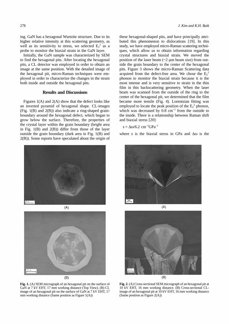
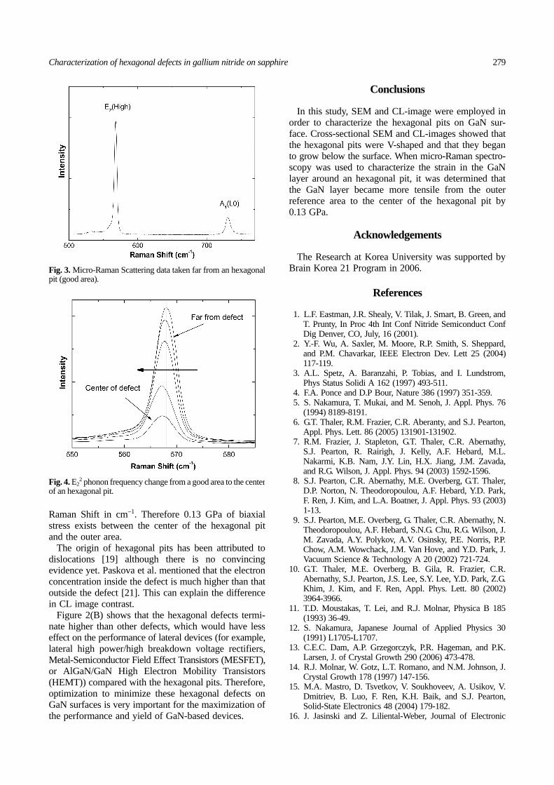
Figures 1(A) and 2(A) show that the defect looks likean inverted pyramid of hexagonal shape. CL-images(Fig. 1(B) and 2(B)) also indicate a ring-shaped grain-boundary around the hexagonal defect, which began togrow below the surface. Therefore, the properties ofthe crystal layer within the grain boundary (bright areain Fig. 1(B) and 2(B)) differ from those of the layeroutside the grain boundary (dark area in Fig. 1(B) and2(B)). Some reports have speculated about the origin of
these hexagonal-shaped pits, and have principally attri-buted this phenomenon to dislocations [19]. In thisstudy, we have employed micro-Raman scattering techni-ques, which allow us to obtain information regardingcrystal structures and biaxial strain. We moved theposition of the laser beam (~2 μm beam size) from out-side the grain boundary to the center of the hexagonalpits. Figure 3 shows the micro-Raman Scattering dataacquired from the defect-free area. We chose the E2
2
phonon to monitor the biaxial strain because it is themost intense and is very sensitive to strain in the thinfilm in this backscattering geometry. When the laserbeam was scanned from the outside of the ring to thecenter of the hexagonal pit, we determined that the filmbecame more tensile (Fig. 4). Lorentzian fitting wasemployed to locate the peak position of the E2
2 phonon,which was decreased by 0.8 cm−1 from the outside tothe inside. There is a relationship between Raman shiftand biaxial stress [20]:
s = Δω/6.2 cm−1GPa−1
where s is the biaxial stress in GPa and Δω is the
Fig. 1. (A) SEM micrograph of an hexagonal pit on the surface ofGaN at 7 kV EHT, 17 mm working distance (Top View). (B) CLimage of an hexagonal pit on the surface of GaN at 7 kV EHT, 17mm working distance (Same position as Figure 1(A))
Fig. 2. (A) Cross-sectional SEM micrograph of an hexagonal pit at10 kV EHT, 16 mm working distance. (B) Cross-sectional CL-image of an hexagonal pit at 10 kV EHT, 16 mm working distance(Same position as Figure 2(A))
Characterization of hexagonal defects in gallium nitride on sapphire 279
Raman Shift in cm−1. Therefore 0.13 GPa of biaxialstress exists between the center of the hexagonal pitand the outer area.
The origin of hexagonal pits has been attributed todislocations [19] although there is no convincingevidence yet. Paskova et al. mentioned that the electronconcentration inside the defect is much higher than thatoutside the defect [21]. This can explain the differencein CL image contrast.
Figure 2(B) shows that the hexagonal defects termi-nate higher than other defects, which would have lesseffect on the performance of lateral devices (for example,lateral high power/high breakdown voltage rectifiers,Metal-Semiconductor Field Effect Transistors (MESFET),or AlGaN/GaN High Electron Mobility Transistors(HEMT)) compared with the hexagonal pits. Therefore,optimization to minimize these hexagonal defects onGaN surfaces is very important for the maximization ofthe performance and yield of GaN-based devices.
Conclusions
In this study, SEM and CL-image were employed inorder to characterize the hexagonal pits on GaN sur-face. Cross-sectional SEM and CL-images showed thatthe hexagonal pits were V-shaped and that they beganto grow below the surface. When micro-Raman spectro-scopy was used to characterize the strain in the GaNlayer around an hexagonal pit, it was determined thatthe GaN layer became more tensile from the outerreference area to the center of the hexagonal pit by0.13 GPa.
Acknowledgements
The Research at Korea University was supported byBrain Korea 21 Program in 2006.
References
1. L.F. Eastman, J.R. Shealy, V. Tilak, J. Smart, B. Green, andT. Prunty, In Proc 4th Int Conf Nitride Semiconduct ConfDig Denver, CO, July, 16 (2001).
2. Y.-F. Wu, A. Saxler, M. Moore, R.P. Smith, S. Sheppard,and P.M. Chavarkar, IEEE Electron Dev. Lett 25 (2004)117-119.
3. A.L. Spetz, A. Baranzahi, P. Tobias, and I. Lundstrom,Phys Status Solidi A 162 (1997) 493-511.
4. F.A. Ponce and D.P Bour, Nature 386 (1997) 351-359.5. S. Nakamura, T. Mukai, and M. Senoh, J. Appl. Phys. 76
(1994) 8189-8191.6. G.T. Thaler, R.M. Frazier, C.R. Aberanty, and S.J. Pearton,
Appl. Phys. Lett. 86 (2005) 131901-131902.7. R.M. Frazier, J. Stapleton, G.T. Thaler, C.R. Abernathy,
S.J. Pearton, R. Rairigh, J. Kelly, A.F. Hebard, M.L.Nakarmi, K.B. Nam, J.Y. Lin, H.X. Jiang, J.M. Zavada,and R.G. Wilson, J. Appl. Phys. 94 (2003) 1592-1596.
8. S.J. Pearton, C.R. Abernathy, M.E. Overberg, G.T. Thaler,D.P. Norton, N. Theodoropoulou, A.F. Hebard, Y.D. Park,F. Ren, J. Kim, and L.A. Boatner, J. Appl. Phys. 93 (2003)1-13.
9. S.J. Pearton, M.E. Overberg, G. Thaler, C.R. Abernathy, N.Theodoropoulou, A.F. Hebard, S.N.G. Chu, R.G. Wilson, J.M. Zavada, A.Y. Polykov, A.V. Osinsky, P.E. Norris, P.P.Chow, A.M. Wowchack, J.M. Van Hove, and Y.D. Park, J.Vacuum Science & Technology A 20 (2002) 721-724.
10. G.T. Thaler, M.E. Overberg, B. Gila, R. Frazier, C.R.Abernathy, S.J. Pearton, J.S. Lee, S.Y. Lee, Y.D. Park, Z.G.Khim, J. Kim, and F. Ren, Appl. Phys. Lett. 80 (2002)3964-3966.
11. T.D. Moustakas, T. Lei, and R.J. Molnar, Physica B 185(1993) 36-49.
12. S. Nakamura, Japanese Journal of Applied Physics 30(1991) L1705-L1707.
13. C.E.C. Dam, A.P. Grzegorczyk, P.R. Hageman, and P.K.Larsen, J. of Crystal Growth 290 (2006) 473-478.
14. R.J. Molnar, W. Gotz, L.T. Romano, and N.M. Johnson, J.Crystal Growth 178 (1997) 147-156.
15. M.A. Mastro, D. Tsvetkov, V. Soukhoveev, A. Usikov, V.Dmitriev, B. Luo, F. Ren, K.H. Baik, and S.J. Pearton,Solid-State Electronics 48 (2004) 179-182.
16. J. Jasinski and Z. Liliental-Weber, Journal of Electronic
Fig. 3. Micro-Raman Scattering data taken far from an hexagonalpit (good area).
Fig. 4. E22 phonon frequency change from a good area to the center
of an hexagonal pit.

280 J. Kim and K.H. Baik
Materials 31 (2002) 429-436.17. C. Wetzel, W. Walukiewicz, E.E. Haller, J. Ager III, I.
Grzegory, S. Porowski, and T. Suski, Physical Review B53 (1996) 1322-1326.
18. T. Kozawa, T. Kachi, H. Kano, H. Nagase, N. Koide, andK. Manabe, Journal of Applied Physics 77 (1995) 4389-4392.
19. T. Kozawa, T. Kaxhi, T. Ohwaki, Y. Taga, N. Koide, and
M. Koide, Journal of Electrochemical Society 143 (1996)L17-L19.
20. W. Rieger, T. Metzger, H. Angerer, R. Dimitrov, O.Ambacher, and M. Stutzmann, Appl. Phys. Lett. 68[7](1996) 970-972.
21. T. Paskova, E.M. Goldys, and B. Monemar, Journal ofCrystal Growth 203 (1999) 1-11.