
Characterization and simulation of electrolyte-gated ...
13
Characterization and simulation of electrolyte-gated organic field-effect transistors Katharina Melzer, * Marcel Br ¨ andlein, Bogdan Popescu, Dan Popescu, Paolo Lugli and Giuseppe Scarpa Received 5th May 2014, Accepted 16th May 2014 DOI: 10.1039/c4fd00095a In this work we fabricate and characterize field-effect transistors based on the solution- processable semiconducting polymer poly(3-hexylthiophene) (P3HT). Applying two independent gate potentials to the electrolyte-gated organic field-effect transistor (EGOFET), by using a conventional SiO 2 layer as the back-gate dielectric and the electrolyte-gate as the top-gate, allows the measurement of the electrical double layer (EDL) capacitance at the semiconductor–electrolyte interface. We record the transfer curves of the transistor in salt solutions of different concentration by sweeping the bottom gate potential for various constant electrolyte-gate potentials. A change of the electrolyte-gate potential towards more negative voltages shifts the threshold voltage of the bottom-gate channel towards more positive back-gate potentials, which is directly proportional to the capacitive coupling factor. By operating the EGOFET in the dual-gate mode, we can prove the dependency of the EDL capacitance on the molarity of the electrolyte according to the Debye–H ¨ uckel theory, and additionally show the difference between a polarizable and non-polarizable electrolyte-gate electrode. With the experimentally obtained values for the EDL capacitance at the semiconductor– electrolyte interface we can model the electrolyte-gate transfer characteristics of the P3HT OTFT. 1 Introduction Organic thin-lm transistors (OTFTs) have been explored for various sensing applications in recent years due to their easy and low-cost fabrication (for recent reviews refer to 1–3 and references therein). In particular, the semiconducting polymer poly(3-hexylthiophene) (P3HT) is well-established as the active semi- conducting component in OTFTs for biosensing applications 4–9 due to several key features offered by the material: its outstanding biocompatibility, 10 its solution Institute for Nanoelectronics, TU M¨ unchen, Arcisstrasse 21, 80333 M¨ unchen, Germany. E-mail: katharina. [email protected] This journal is © The Royal Society of Chemistry 2014 Faraday Discuss. , 2014, 174, 399–411 | 399 Faraday Discussions Cite this: Faraday Discuss. , 2014, 174, 399 PAPER Open Access Article. Published on 02 June 2014. Downloaded on 2/10/2022 1:13:24 AM. This article is licensed under a Creative Commons Attribution 3.0 Unported Licence. View Article Online View Journal | View Issue
Transcript of Characterization and simulation of electrolyte-gated ...
Faraday DiscussionsCite this: Faraday Discuss., 2014, 174, 399
PAPER
Ope
n A
cces
s A
rtic
le. P
ublis
hed
on 0
2 Ju
ne 2
014.
Dow
nloa
ded
on 2
/10/
2022
1:1
3:24
AM
. T
his
artic
le is
lice
nsed
und
er a
Cre
ativ
e C
omm
ons
Attr
ibut
ion
3.0
Unp
orte
d L
icen
ce.
View Article OnlineView Journal | View Issue
Characterization and simulation ofelectrolyte-gated organic field-effecttransistors
Katharina Melzer,* Marcel Brandlein, Bogdan Popescu, Dan Popescu,Paolo Lugli and Giuseppe Scarpa
Received 5th May 2014, Accepted 16th May 2014
DOI: 10.1039/c4fd00095a
In this work we fabricate and characterize field-effect transistors based on the solution-
processable semiconducting polymer poly(3-hexylthiophene) (P3HT). Applying two
independent gate potentials to the electrolyte-gated organic field-effect transistor
(EGOFET), by using a conventional SiO2 layer as the back-gate dielectric and the
electrolyte-gate as the top-gate, allows the measurement of the electrical double layer
(EDL) capacitance at the semiconductor–electrolyte interface. We record the transfer
curves of the transistor in salt solutions of different concentration by sweeping the
bottom gate potential for various constant electrolyte-gate potentials. A change of the
electrolyte-gate potential towards more negative voltages shifts the threshold voltage
of the bottom-gate channel towards more positive back-gate potentials, which is
directly proportional to the capacitive coupling factor. By operating the EGOFET in the
dual-gate mode, we can prove the dependency of the EDL capacitance on the molarity
of the electrolyte according to the Debye–Huckel theory, and additionally show the
difference between a polarizable and non-polarizable electrolyte-gate electrode. With
the experimentally obtained values for the EDL capacitance at the semiconductor–
electrolyte interface we can model the electrolyte-gate transfer characteristics of the
P3HT OTFT.
1 Introduction
Organic thin-lm transistors (OTFTs) have been explored for various sensingapplications in recent years due to their easy and low-cost fabrication (for recentreviews refer to1–3 and references therein). In particular, the semiconductingpolymer poly(3-hexylthiophene) (P3HT) is well-established as the active semi-conducting component in OTFTs for biosensing applications4–9 due to several keyfeatures offered by the material: its outstanding biocompatibility,10 its solution
Institute for Nanoelectronics, TU Munchen, Arcisstrasse 21, 80333 Munchen, Germany. E-mail: katharina.
This journal is © The Royal Society of Chemistry 2014 Faraday Discuss., 2014, 174, 399–411 | 399

Faraday Discussions PaperO
pen
Acc
ess
Art
icle
. Pub
lishe
d on
02
June
201
4. D
ownl
oade
d on
2/1
0/20
22 1
:13:
24 A
M.
Thi
s ar
ticle
is li
cens
ed u
nder
a C
reat
ive
Com
mon
s A
ttrib
utio
n 3.
0 U
npor
ted
Lic
ence
.View Article Online
processability and subsequent applicability in large-scale, exible and cost-effective electronics, and its relatively high mobility.11,12
In organic thin-lm transistors, in general a thin lm of an organic semi-conducting material is utilized as the active layer. Two contacts, the source anddrain electrodes, which are in direct contact with the semiconducting material,are used to apply the source–drain voltage and to measure the current owingbetween them through the organic semiconducting channel. As the third elec-trode, the gate electrode is used to control the number of charge carriers, in p-typematerial holes, in the semiconducting channel at the interface between thesemiconductor and the gate dielectric through an electric eld applied across theinsulating gate dielectric. Therefore one can modulate the source–drain currentowing between the source and drain contacts by applying a given potential to thegate electrode. For a p-type material the transistor is turned “ON” for negative gatevoltages, whereas a positive gate bias switches the device “OFF”.13
In recent years the usage of solid and liquid electrolytes as gate dielectrics inOTFTs has gained great interest. They display a huge capacitance (CG) comparedto the conventional silicon dioxide (SiO2), which is typically in the range of 1–100mF cm�2,�1000 times higher than the one offered by a nm-thick SiO2-layer.1,12,14,15
Especially important in EGOFETs is the formation of an electrical double layer(EDL) at the electrolyte–semiconductor interface as well as the gate electrode–electrolyte interface. At the gate electrode–electrolyte interface the electroniccharges close to the electrode surface are compensated by oppositely charged ionsin the electrolyte close to the interface. At the electrolyte–semiconductor interfacethe EDL consists of ions forming the inner Helmholtz plane in the electrolyte andcharge carriers in the semiconducting channel. Additionally, at both interfaces,hydrated ions of both charges accumulate and form the outer Helmholtz plane. Inthe bulk of the electrolyte, the potential stays constant as the diffuse layer of thehydrated positive and negative ions ensures charge neutrality.12,15,16 The chargedistribution in an EDL can be described by the Gouy–Chapman–Stern model.17–20
In the case of a at electrode surface, the electrostatic capacitance of the EDL canbe related to the Debye length lD, which denes the distance d between theinterface and the outermost layer of ions which is necessary to compensate thegate surface charge fully. The Debye length is inversely proportional to the squareroot of the ionic strength, according to:
CDL � 1
lD(1)
lD ¼ffiffiffiffiffiffiffiffiffiffiffiffiffiffiffiffiffiffi3r30kBT
2C0NAe2
s(2)
where CDL represents the capacitance of the electrical double layer, lD is theDebye length, the parameters 3r and 30 are the relative and the vacuum permit-tivity, respectively, kB is the Boltzmann constant, T is the temperature, C0 is theionic strength of the electrolyte, NA is the Avogadro constant and e is theelementary charge.19 Since the thickness of the electrical double layer is on thesub-nm length scale (a few A to nm), the capacitance per unit area is typically inthe range of tens of mF cm�2. This huge gate capacitance allows a transistor tooperate at very low voltages: already gate potentials of around 0.5 V are sufficient
400 | Faraday Discuss., 2014, 174, 399–411 This journal is © The Royal Society of Chemistry 2014

Paper Faraday DiscussionsO
pen
Acc
ess
Art
icle
. Pub
lishe
d on
02
June
201
4. D
ownl
oade
d on
2/1
0/20
22 1
:13:
24 A
M.
Thi
s ar
ticle
is li
cens
ed u
nder
a C
reat
ive
Com
mon
s A
ttrib
utio
n 3.
0 U
npor
ted
Lic
ence
.View Article Online
to accumulate enough charge carriers in the semiconducting channel to turn thedevice “ON”. By exploiting the electrical double layer capacitance one canmodulate the transistor current response extremely effectively. Another veryimportant advantage of electrolyte-gated organic thin-lm transistors is theconvenient integration into biosensors operated in liquid environments. One is infact independent from the choice of the substrate,21,22 and the analyte is already indirect contact with the active semiconducting layer. Since the accumulation ofcharge carriers in the semiconducting channel and therefore also the source–drain current can be altered by the adsorption of charged analytes on the semi-conductor surface or a change in the amount of solute ions in the electrolyte,electrical detection of certain species is possible.
Therefore it is of great interest for various sensing applications with EGOFETsto obtain information about how changes to the electrolyte–semiconductorinterface, especially to the electrical double layer and its capacitance, inuencethe transistor characteristics.
In this work we concentrate on the inuence of the electrical double-layercapacitance (CDL) and try to gain information about the dependency of CDL on theionic strength of the electrolyte. We operate the OTFT based on the semicon-ducting polymer poly(3-hexylthiophene) (P3HT) in the so-called dual-gate mode23
by using both a conventional back-gate as well as an electrolyte-gate as the top-gate. Exploiting the capacitive coupling factor23,24 allows us to extract the double-layer capacitance from several back-gate sweeps with different constant electro-lyte-gate potentials. Changing the ionic strength of the aqueous potassiumchloride (KCl) solution used as the gate dielectric for the electrolyte-gate gives usthe double-layer capacitance as a function of the salt concentration. Wedemonstrate that the capacitance of the electrical double layer at the semi-conductor–electrolyte interface increases with an exponential increase of theionic strength of the electrolyte. In addition to the electrical characterization ofthe organic thin-lm transistors, we compare the results to theoretical datagained from simulations with a modied dri–diffusion model.
2 Experimental2.1 Device fabrication
Organic thin-lm transistors (OTFTs) were processed using highly p-dopedsilicon wafers (Si-Mat) as a substrate with a thermally grown 65 nm thick silicondioxide layer (SiO2) as the conventional gate dielectric. Source and drain elec-trodes (5 nm Cr as adhesion layer, 40 nm Au) were patterned on top of the oxidelayer by a conventional negative optical photolithography process. An interdigi-tated nger structure (IDES) was used as the electrode structure, with a channellength of 50 mm and a width-to-length ratio of 900. A 1 wt% solution of regiore-gular poly(3-hexylthiophene) (P3HT, Rieke Metals) in anhydrous 1,2-dichloro-benzene (DCB, VWR) was prepared and stirred for 30 min to obtain ahomogeneous solution. The solution was then ltered through a polytetra-uoroethylene (PTFE) syringe lter with a pore size of 200 nm (VWR) and spin-coated (1000 rpm, 90 s) onto the surface of the wafer in a glove box system (N2).Aer spin-coating, the lm was annealed on a hot plate under a nitrogen atmo-sphere at 150 �C for 20 min. The obtained polymer layer was approximately 50 to70 nm thick. Atomic force microscopy (AFM, Jeol, JSPM-5200) measurements
This journal is © The Royal Society of Chemistry 2014 Faraday Discuss., 2014, 174, 399–411 | 401

Faraday Discussions PaperO
pen
Acc
ess
Art
icle
. Pub
lishe
d on
02
June
201
4. D
ownl
oade
d on
2/1
0/20
22 1
:13:
24 A
M.
Thi
s ar
ticle
is li
cens
ed u
nder
a C
reat
ive
Com
mon
s A
ttrib
utio
n 3.
0 U
npor
ted
Lic
ence
.View Article Online
yielded an Rq value of 3.4 nm, which is a measure for the surface roughness of thepolymeric lm, and a peak-to-valley distance of about 22 nm.
2.2 Electrical characterization
Transfer characteristics (ID vs. VG) and output characteristics (ID vs. VDS) of thedevices were recorded using a Keithley 4200-SCS semiconductor parameter ana-lyser system. To operate the transistor in liquid, measurements were performedaer mounting the devices in a PDMS ow-chamber, which has a liquidcompartment volume of 100 mL. The transfer characteristics of the OTFT wereobtained by sweeping either the back-gate potential (VDS ¼ �10 V) or the elec-trolyte-gate potential (VDS ¼ �0.1 V), while a constant drain voltage VDS wasapplied. For the back-gate sweep no electrolyte was on top of the semiconductinglayer, whereas for the electrolyte-gate sweep the back-gate electrode was leoating. The electrolyte-gate potential was chosen from the relatively smallvoltage regime between VTgS ¼ +0.6 V and VTgS ¼ �0.6 V to avoid any waterhydrolysis or any other electrochemical reaction at the gate electrode or thesemiconductor surface.12
For the measurement of the electrical double layer capacitance, the potentialat the electrolyte-gate electrode, either a Pt wire or a homemade Ag/AgCl elec-trode, was kept constant while a scan of the back-gate voltage between VBgS ¼ +20V and VBgS ¼ �7.5 V was performed. The back-gate sweep was recorded for sixdifferent electrolyte-gate potentials between VTgS ¼ +0.1 V and VTgS ¼ �0.4 V,whereas the drain voltage was kept constant for each back-gate sweep at VDS ¼�0.1 V. All characterization measurements were performed in ambient condi-tions. The electrolyte was exchanged manually using a Gilson pipette. Aerexchanging the electrolyte the system was le to equilibrate for 5 minutes beforethe next measurement was started.
2.3 Preparation of electrolytes
The electrical double layer capacitance was characterized using either deionizedwater (DI-H2O, classied with a resistivity of 18.2 MU cm). Potassium chloridesolutions were prepared by dissolving 100mMKCl ($99.0%, Sigma Aldrich) in DI-H2O and further diluting it with DI-H2O to the desired KCl concentrations.
3 Results and discussion3.1 Device characteristics
The transfer characteristics of the OTFT were obtained by sweeping either theback-gate potential or the electrolyte-gate potential, while a constant drain voltageVDS was applied. For the back-gate sweep no electrolyte was on top of the semi-conducting layer, whereas for the electrolyte-gate sweep the back-gate electrodewas le oating. Fig. 1(a) shows the source–drain current ID versus the back-gatepotential; the drain voltage was kept constant at VDS ¼ �10 V. Fig. 1(b) shows IDversus the electrolyte-gate potential VTgS of the OTFT gated with a Pt electrode in a10 mM solution of KCl in DI-water as the electrolyte; the drain voltage was keptconstant at VDS ¼ �0.1 V. Both transfer curves exhibit typical p-type eld-effectcharacteristics with ON/OFF ratios of around 100. When the OTFT is operatedwith the conventional silicon dioxide (SiO2, 65 nm, COx¼ 53.2 nF cm�2) back-gate,
402 | Faraday Discuss., 2014, 174, 399–411 This journal is © The Royal Society of Chemistry 2014
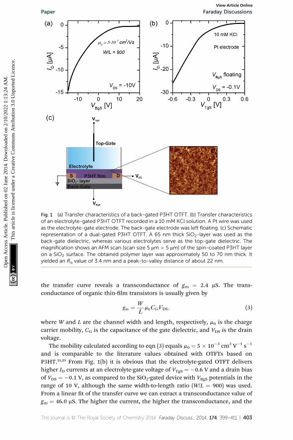
Fig. 1 (a) Transfer characteristics of a back-gated P3HT OTFT. (b) Transfer characteristicsof an electrolyte-gated P3HT OTFT recorded in a 10 mM KCl solution. A Pt wire was usedas the electrolyte-gate electrode. The back-gate electrode was left floating. (c) Schematicrepresentation of a dual-gated P3HT OTFT. A 65 nm thick SiO2-layer was used as theback-gate dielectric, whereas various electrolytes serve as the top-gate dielectric. Themagnification shows an AFM scan (scan size 5 mm � 5 mm) of the spin-coated P3HT layeron a SiO2 surface. The obtained polymer layer was approximately 50 to 70 nm thick. Ityielded an Rq value of 3.4 nm and a peak-to-valley distance of about 22 nm.
Paper Faraday DiscussionsO
pen
Acc
ess
Art
icle
. Pub
lishe
d on
02
June
201
4. D
ownl
oade
d on
2/1
0/20
22 1
:13:
24 A
M.
Thi
s ar
ticle
is li
cens
ed u
nder
a C
reat
ive
Com
mon
s A
ttrib
utio
n 3.
0 U
npor
ted
Lic
ence
.View Article Online
the transfer curve reveals a transconductance of gm ¼ 2.4 mS. The trans-conductance of organic thin-lm transistors is usually given by
gm ¼ W
Lm0CGVDS; (3)
where W and L are the channel width and length, respectively, m0 is the chargecarrier mobility, CG is the capacitance of the gate dielectric, and VDS is the drainvoltage.
The mobility calculated according to eqn (3) equals m0 ¼ 5 � 10�3 cm2 V�1 s�1
and is comparable to the literature values obtained with OTFTs based onP3HT.11,25 From Fig. 1(b) it is obvious that the electrolyte-gated OTFT delivershigher ID currents at an electrolyte-gate voltage of VTgS ¼ �0.6 V and a drain biasof VDS ¼ �0.1 V, as compared to the SiO2-gated device with VBgS potentials in therange of 10 V, although the same width-to-length ratio (W/L ¼ 900) was used.From a linear t of the transfer curve we can extract a transconductance value ofgm ¼ 46.0 mS. The higher the current, the higher the transconductance, and the
This journal is © The Royal Society of Chemistry 2014 Faraday Discuss., 2014, 174, 399–411 | 403

Faraday Discussions PaperO
pen
Acc
ess
Art
icle
. Pub
lishe
d on
02
June
201
4. D
ownl
oade
d on
2/1
0/20
22 1
:13:
24 A
M.
Thi
s ar
ticle
is li
cens
ed u
nder
a C
reat
ive
Com
mon
s A
ttrib
utio
n 3.
0 U
npor
ted
Lic
ence
.View Article Online
lower operating voltages reect the greatly enlarged gate capacitance of theelectrical double layer relative to the 65 nm thick SiO2-layer. In order to derive themobility from the transfer curves of the electrolyte-gated OTFT, we rst have tomeasure the capacitance of the electrical double layer.
3.2 Measurement of the electrical double layer capacitance
To measure the capacitance of the electrical double layer, we operate the OTFT inthe so-called dual-gate mode23 by using both the conventional silicon dioxide(SiO2, 65 nm) back-gate as well as an additional electrolyte-gate. The transfercurves (ID vs. VBgS) of the back-gated transistor can be shied by applying variousxed voltages to the electrolyte-gate electrode immersed in an aqueous solution(see Fig. 1(c)). Here the potential at the electrolyte-gate electrode was keptconstant, while a sweep of the back-gate voltage was performed between VBgS ¼+20 V and VBgS ¼ �7.5 V. If the applied electrolyte-gate voltage is negative, asemiconducting channel at the electrolyte–polymer interface is formed and thecharge carrier accumulation in the semiconducting layer can be controlled bysweeping the back-gate voltage. A back-gate sweep was recorded for six differentelectrolyte-gate potentials between VTgS ¼ 0.1 V and VTgS ¼ �0.4 V. The resultingtransfer curves with DI-water as the electrolyte and a Pt wire as the gate electrodeare shown in Fig. 2(a). The obtained transfer curves rst exhibit a short chargingphase and then follow a linear dependence for ID vs. VBgS. According to a theo-retical model for dual gate transistors,24 the source–drain current of a dual-gatedOTFT in the linear regime can be expressed as follows:23
ID ¼ W
Lm0
�CDLVTgS þ COxVBgS þ si
�VDS; (4)
where W is the width and L is the length of the channel, m0 is the mobility, COx isthe capacitance of the SiO2 layer, CDL is the electrical double layer capacitance,and VDS, VTgS and VBgS are the drain voltage, the electrolyte-gate potential and theback-gate potential, respectively. According to eqn (4), the threshold voltage of theback-gate sweep VBG,th, which is dened as the back-gate voltage where the
Fig. 2 (a) Back-gate transfer curves (black lines) at VDS¼�0.1 V recorded in DI-water witha Pt gate electrode and linear fits (red lines) at different electrolyte-gate voltages VTgS. (b)Threshold voltages extracted from the linear fit curves of the back-gate sweeps as afunction of the electrolyte-gate potential and the corresponding linear fit curve.
404 | Faraday Discuss., 2014, 174, 399–411 This journal is © The Royal Society of Chemistry 2014

Paper Faraday DiscussionsO
pen
Acc
ess
Art
icle
. Pub
lishe
d on
02
June
201
4. D
ownl
oade
d on
2/1
0/20
22 1
:13:
24 A
M.
Thi
s ar
ticle
is li
cens
ed u
nder
a C
reat
ive
Com
mon
s A
ttrib
utio
n 3.
0 U
npor
ted
Lic
ence
.View Article Online
source–drain current equals zero, is directly proportional to the applied electro-lyte-gate potential modulated by the capacitive coupling factor CDL/COx:23
VBG;th f� CDL
COX
VTgS: (5)
The threshold voltages were extrapolated from a linear t (red lines, Fig. 2(a))of the various transfer curves and plotted as a function of the applied top-gatevoltage VTgS, as depicted in Fig. 2(b).
By using the slope k obtained from the linear t of the VBG,th vs. VTgS depen-dence and taking into account the capacitance of the back-gate dielectric(thickness dOx ¼ 65 nm, COx ¼ 53.2 nF cm�2), the capacitance of the electricaldouble layer can be calculated according to eqn (5) (ref. 23).
We obtain a double layer capacitance of CDL (DI-H2O) ¼ 10.8 � 1.2 mF cm�2,which exceeds the literature values for P3HT in contact with deionized water (3–6mF cm�2), as measured by impedance spectroscopy, by a factor of 2, but they areconsistent with values obtained for metallic surfaces in contact with an electro-lyte, �20 mF cm�2 for gold in contact with DI-water.12 Cramer et al.23 determinedthe double layer capacitance with a pentacene thin-lm transistor with deionizedwater as the electrolyte. They obtained values of CDL (DI-H2O) ¼ 7.8 mF cm�2,23
which is generally lower than the results obtained with the P3HT OTFT. Onepossible explanation could be that their semiconducting layer consists of lessthan six monolayers of pentacene and therefore has a much smoother surfacethan the P3HT lm (see the AFM image in Fig. 1(c)) used in this work. Insimplied terms, the huge surface roughness of the P3HT lm results in anincreased capacitance of the electrical double layer at the semiconductor–elec-trolyte interface since the geometrical size of the active area (4 mm � 4 mm) staysconstant, whereas the effective contact area between the electrolyte and semi-conductor increases with increasing surface roughness.
In general, the capacitance of the Debye–Helmholtz layer depends on the ionicstrength of the electrolytic solution (see eqn (1) and (2)), therefore back-gatesweeps were not only recorded for different top-gate voltages but also in KClsolutions with varying ion concentrations. The obtained values for the doublelayer capacitance measured with a Pt wire as the gate electrode are shown inFig. 3(a). The reduction of the capacitance to lower ionic strengths is in generalagreement with theoretical models describing the Debye–Helmholtz layer.17–19
Again, the value obtained by Cramer et al.23 for a 100 mM solution of a mono-valent salt (sodium chloride, NaCl) CDL (100 mM NaCl) ¼ 14.6 mF cm�2 is lowerthan the EDL capacitance measured with the P3HT OTFT.
Additionally, the same measurements were performed with an Ag/AgCl elec-trode. The main difference between these two gate materials is that platinum canbe seen as an ideally polarizable electrode when operated in an electrolyticsolution with these relatively low voltages (|VTgS| < 1 V), which means that anelectrical double layer forms at the interface between the gate-material and theelectrolyte. However, due to the following reaction constantly taking place at thesurface of the Ag/AgCl electrode, a steady-state current ows from the gate elec-trode to the electrolytic solution, and therefore no electrical double layer forms atthe interface between the electrode and the electrolyte.26
This journal is © The Royal Society of Chemistry 2014 Faraday Discuss., 2014, 174, 399–411 | 405

Fig. 3 Capacitance of the electrical double layer CDL obtained (a) for a Pt-gated transistorand (b) with an Ag/AgCl electrode as the gate electrode as a function of the saltconcentration. Panel (c) shows the equivalent circuits28 of a Pt gate electrode and an Ag/AgCl electrode immersed in the electrolytic solution. The right graph depicts the potentialdistribution between the gate electrode and the semiconducting channel for both elec-trode types.26
Faraday Discussions PaperO
pen
Acc
ess
Art
icle
. Pub
lishe
d on
02
June
201
4. D
ownl
oade
d on
2/1
0/20
22 1
:13:
24 A
M.
Thi
s ar
ticle
is li
cens
ed u
nder
a C
reat
ive
Com
mon
s A
ttrib
utio
n 3.
0 U
npor
ted
Lic
ence
.View Article Online
Ag + Cl� 4 AgCl + e� (6)
This means that with a Pt wire immersed as the gate electrode in the elec-trolytic solution, the applied gate potential drops across two electrical doublelayers formed both at the electrode–electrolyte interface as well as at the elec-trolyte–semiconductor interface. On the contrary, for an Ag/AgCl electrode thewhole potential has to drop across the electrical double layer formed at theelectrolyte–semiconductor interface (see Fig. 3(c)).19,20,27,28
In a simple equivalent circuit, the Pt wire immersed in the electrolytic solutioncan be regarded as a capacitor CG (see Fig. 3(c)), which is connected in series withthe capacitor CDL of the interface between the P3HT layer and the electrolyticsolution, as shown in Fig. 3(a). Thus the effective gating capacitance of the OTFToperated with a Pt electrode is given by:28
Ceff ;Pt ¼ CGCDL
CG þ CDL
: (7)
Therefore one would expect to measure a higher double layer capacitance CDL
by operating the device with an Ag/AgCl electrode. Fig. 3(b) shows the double layercapacitance measured with an Ag/AgCl electrode as a function of the saltconcentration present in the electrolyte.
For a KCl concentration of 100 mMwe obtain a double layer capacitance of CDL
(100 mM KCl, Ag/AgCl) ¼ 123.77 � 2.50 mF cm�2, which is about 4 times higherthan with a Pt electrode, where CDL (100 mM KCl, Pt) ¼ 33.78 � 5.25 mF cm�2.
406 | Faraday Discuss., 2014, 174, 399–411 This journal is © The Royal Society of Chemistry 2014

Paper Faraday DiscussionsO
pen
Acc
ess
Art
icle
. Pub
lishe
d on
02
June
201
4. D
ownl
oade
d on
2/1
0/20
22 1
:13:
24 A
M.
Thi
s ar
ticle
is li
cens
ed u
nder
a C
reat
ive
Com
mon
s A
ttrib
utio
n 3.
0 U
npor
ted
Lic
ence
.View Article Online
3.3 Simulation of electrolyte-gated eld-effect transistors
For the simulation of the back-gated and electrolyte-gated OTFT devices we use amodied dri–diffusion model implemented into the commercial TCAD sowareSentaurus. For a given device geometry, this soware simulates charge transportby solving a set of equations, including the dri–diffusion equations, the conti-nuity equations and the Poisson equation
Jn ¼ �emnVf + eDnVn, (8)
JP ¼ �empVf � eDpVp, (9)
V$Jn ¼ e(R � G), (10)
V$Jp ¼ �e(R � G), (11)
V$(303rVf) ¼ e(n � p + N+D � N�
A + pAt), (12)
where Jn (Jp) is the electron (hole) current density, n (p) is the electron (hole)density, mn (mp) is the electron (hole) mobility, Dn (Dp) is the electron (hole)diffusion coefficient, f is the electrostatic potential, G and R are the net genera-tion and recombination rates and pAt is the density of trapped holes. To accountfor the particularities of organic materials, three modications are imple-mented.29,30 Firstly, a low contact barrier height from the source to HOMO level ofthe semiconductor material ensures easy injection of holes, giving the device p-type conductivity. Secondly, a Poole–Frenkel-type eld-dependent mobility needsto be considered:
m ¼ m0ðTÞexp� ffiffiffiffiffiffiffiffiffiffiffi
E=E0
p �; (13)
where m0(T) is the low eld mobility, E is the electric eld and E0 is an effectiveparameter of approximately 3 � 105 V cm�1. Thirdly, an interface trap model atthe oxide–P3HT interface and the electrolyte–semiconductor interface effectivelymodels the hopping-assisted charge transport. Here, an exponential energydistribution of two different trap levels, a shallow trap at 0.1 eV and a deeper trapat 0.4 eV, from the HOMO level is considered. Such a broad energy distribution isjustied by the use of standard spin-coating techniques for the deposition of theorganic semiconductor, inevitably introducing defects into the P3HT activeregion.
In a rst approximation, the electrolyte will be taken into account as aninsulating layer between the electrolyte-gate contact and the organic semi-conductor region, according to the simple Helmholtz model (see Fig. 4(a)).31
That way, the electrical double layer is modelled as a parallel plate capacitor(from here on referred to as the Helmholtz layer) accounting for a linear potentialdrop. The capacitance of this Helmholtz layer is taken from the experimentallyextracted data to 28 mF cm�2 for an ion concentration of 10 mM, according toSection 3.2. As can be seen in Fig. 4(b), when operating with the top-gate contactthe conductive channel is spatially shied towards the electrolyte–semiconductorinterface. This can be intuitively understood considering the electric eld that isgenerated by the applied negative top-gate voltage and which attracts positivecharge carriers towards this interface. The considerably low top-gate voltage is
This journal is © The Royal Society of Chemistry 2014 Faraday Discuss., 2014, 174, 399–411 | 407

Fig. 4 (a) Drift–diffusion simulation layout for the Helmholtz model. The electrolyte istaken into account by an insulating Helmholtz layer. (b) Comparison of back-gate oper-ation and top-gate operation. The values of the boundary conditions are given at therespective contacts and are typical for the different operation modes. The hole densitygives information as to where the conducting channel is formed.
Faraday Discussions PaperO
pen
Acc
ess
Art
icle
. Pub
lishe
d on
02
June
201
4. D
ownl
oade
d on
2/1
0/20
22 1
:13:
24 A
M.
Thi
s ar
ticle
is li
cens
ed u
nder
a C
reat
ive
Com
mon
s A
ttrib
utio
n 3.
0 U
npor
ted
Lic
ence
.View Article Online
due to the large capacitive value of the Helmholtz layer compared to the oxidelayer of the back-gate contact.
With this simulation setup, we simulate transfer and output curves in bothback-gate and top-gate operation and compare them to experimental data toadjust the simulation parameters. The simulation of the back-gate operation hasalready been reported in the literature,32 and serves as a reference for the simu-lation parameters of the organic semiconductor material, such as density ofstates, unintentional doping, trap level distribution, low eld mobility etc. Theseparameters are then used for the simulation of top-gate operation to give aconclusive self-consistent picture. All relevant simulation parameters are given inTable 1. The results of such a tting procedure are shown in Fig. 5 for one selecteddevice. The simulation of transfer curves in back-gate operation (Fig. 5(a)) showsgood agreement with the experimental data in the accessible voltage range, andalso the output curve is in the right order of magnitude. The low eld mobility inthat case is m0 ¼ 5 � 10�3 cm2 V�1 s�1, which is in good agreement with literaturevalues.11,25 When simulating the top-gate operation (Fig. 5(b)), one can see thatusing this value for the low eld mobility leads to a drastic underestimation of thedrain current. There are two parameters in our model which affect the trans-conductance of the device, i.e. the slope of the linear transistor behaviour, the rstbeing the capacitance of the Helmholtz layer and the second being the low eldmobility. By changing the Helmholtz layer capacitance one would have to useunphysical values that are several orders of magnitude larger than what has beenextracted experimentally, in order to t the experimental data. Furthermore, thisleads to large deviations from the experimental data in the sublinear regime asthe curve becomes heavily kinked.
On the other hand, when changing the mobility by about one order ofmagnitude, the transconductance of the experimental data can be matchedcorrectly and also the deviations in the sublinear regime are not as pronounced.Such an elevated low eld mobility hints at a physical change in the transportproperties at the electrolyte–semiconductor interface. Cramer et al.33 stated thatthe reorientation of water dipoles at the electrolyte–semiconductor interfacestabilizes positive charge carriers and leads to a polaronic trap state which
408 | Faraday Discuss., 2014, 174, 399–411 This journal is © The Royal Society of Chemistry 2014

Table 1 Simulation parameters for back-gate and top-gate operation
Device T#01
P3HT LUMO 3 eVHOMO 5 eV3r 3DOS 5 � 1020 cm�3
Doping concentration ND 1.2 � 1017 cm�3
Poole–Frenkel mobility m0 (back) 5 � 10�3 cm2 V�1 s�1
m0 (top) 3 � 10�2 cm2 V�1 s�1
E0 3 � 105 V cm�1
Shallow level trap c0,shall 5 � 1012 cm�2
Emid 0.1 eVEsig 0.2 eV
Deep level trap c0,deep 5 � 1012 cm�2
Emid 0.4 eVEsig 0.3 eV
Fixed charges cx (back) �2.1 � 1012 cm�2
cx (top) �2.1 � 1012 cm�2
Paper Faraday DiscussionsO
pen
Acc
ess
Art
icle
. Pub
lishe
d on
02
June
201
4. D
ownl
oade
d on
2/1
0/20
22 1
:13:
24 A
M.
Thi
s ar
ticle
is li
cens
ed u
nder
a C
reat
ive
Com
mon
s A
ttrib
utio
n 3.
0 U
npor
ted
Lic
ence
.View Article Online
remains highly mobile in the plane parallel to the interface. Their ndings basedon pentacene show a mobility elevated by about one order of magnitude.
They mention that the polaron binding energy depends only on water polari-zation and the spatial extension of the charge carriers in the organic semi-conductor. Therefore, these ndings can be generalized to other organicsemiconductors and might give an explanation for the different mobilities forback-gate operation versus top-gate operation in our sensor devices. However,further investigations are needed in that direction.
In order to rene the simple approximation of the EDL as a parallel platecapacitor, one needs to account for a diffusive layer, the Gouy–Chapman layer, in
Fig. 5 (a) Best fit of the back-gate operation transfer curve for one selected device. Theinset shows an output curve at VBgS ¼�10 V. The mobility is m0 ¼ 5� 10�3 cm2 V�1 s�1. (b)Fit of the top-gate operation transfer curve for device T#01 for different low fieldmobilities according to the Helmholtz model. The ion concentration in the electrolyte is10 mM. All simulation parameters can be found in Table 1.
This journal is © The Royal Society of Chemistry 2014 Faraday Discuss., 2014, 174, 399–411 | 409

Faraday Discussions PaperO
pen
Acc
ess
Art
icle
. Pub
lishe
d on
02
June
201
4. D
ownl
oade
d on
2/1
0/20
22 1
:13:
24 A
M.
Thi
s ar
ticle
is li
cens
ed u
nder
a C
reat
ive
Com
mon
s A
ttrib
utio
n 3.
0 U
npor
ted
Lic
ence
.View Article Online
the form of the Poisson–Boltzmann equation (PBe) according to the Sternmodel.34 The PBe reads
Vð303rVfÞ ¼ �XNi¼1
zieci;0exp
�� zie
�f� VTgS
�kBT
�; (14)
where the sum goes over all ion species present in the electrolyte, zi is the valencyand ci,0 the bulk concentration of ion species i. This is already under investigationand will be the topic of a future contribution.
4 Conclusion
In summary, we reported the measurement of the electrical double layer capac-itance of a dual-gated P3HT OTFT by sweeping the back-gate potential with xedelectrolyte-gate potentials at the top-gate. We proved the dependency of the EDLcapacitance on the ionic strength of the electrolyte and additionally we demon-strated the effect of a non-polarizable gate electrode in comparison to a polariz-able electrode on the gating mechanism. With the experimentally obtained valuesfor the capacitance of the Debye-Helmholtz layer at the semiconductor–electrolyteinterface, we can model the electrolyte-gate transfer characteristics of the P3HTOTFT. Our study suggests that the mobility of the active material close to thesemiconductor–electrolyte interface is larger than the bulk mobility.
Acknowledgements
This work was partially supported by the International Graduate School forScience and Engineering (IGSSE), the Graduate School (TUM-GS) at the Techni-sche Universitat Munchen, and the European Integrated Training Networks“Olimpia” and “OrgBio”.
References
1 L. Kergoat, B. Piro, M. Berggren, G. Horowitz and M.-C. Pham, Anal. Bioanal.Chem., 2012, 402, 1813–1826.
2 P. Lin and F. Yan, Adv. Mater., 2012, 24, 34–51.3 J. T. Mabeck and G. G. Malliaras, Anal. Bioanal. Chem., 2006, 384, 343–353.4 A. M. Munzer, K. Melzer, M. Heimgreiter and G. Scarpa, Biochim. Biophys. Acta,2013, 1830, 4353–4358.
5 C. Bartic, B. Palan, A. Campitelli and G. Borghs, Sens. Actuators, B, 2002, 83,115–122.
6 M. E. Roberts, S. C. B. Mannsfeld, N. Queralto, C. Reese, J. Locklin, W. Knolland Z. Bao, Proc. Natl. Acad. Sci. U. S. A., 2008, 105, 12134–12139.
7 S. Casalini, F. Leonardi, T. Cramer and F. Biscarini, Org. Electron., 2013, 14,156–163.
8 M. D. Angione, S. Cotrone, M. Magliulo, A. Mallardi, D. Altamura, C. Giannini,N. Cioffi, L. Sabbatini, E. Fratini, P. Baglioni, G. Scamarcio, G. Palazzo andL. Torsi, Proc. Natl. Acad. Sci. U. S. A., 2012, 109, 6429–6434.
9 M. Magliulo, A. Mallardi, M. Y. Mulla, S. Cotrone, B. R. Pistillo, P. Favia,I. Vikholm-Lundin, G. Palazzo and L. Torsi, Adv. Mater., 2013, 25, 2090–2094.
410 | Faraday Discuss., 2014, 174, 399–411 This journal is © The Royal Society of Chemistry 2014
Paper Faraday DiscussionsO
pen
Acc
ess
Art
icle
. Pub
lishe
d on
02
June
201
4. D
ownl
oade
d on
2/1
0/20
22 1
:13:
24 A
M.
Thi
s ar
ticle
is li
cens
ed u
nder
a C
reat
ive
Com
mon
s A
ttrib
utio
n 3.
0 U
npor
ted
Lic
ence
.View Article Online
10 G. Scarpa, A.-L. Idzko, S. Gotz and S. Thalhammer,Macromol. Biosci., 2010, 10,378–383.
11 S. M. Goetz, C. M. Erlen, H. Grothe, B. Wolf, P. Lugli and G. Scarpa, Org.Electron., 2009, 10, 573–580.
12 L. Kergoat, L. Herlogsson, D. Braga, B. Piro, M.-C. Pham, X. Crispin,M. Berggren and G. Horowitz, Adv. Mater., 2010, 22, 2565–2569.
13 H. Klauk, Chem. Soc. Rev., 2010, 39, 2643–2666.14 S. H. Kim, K. Hong, W. Xie, K. H. Lee, S. Zhang, T. P. Lodge and C. D. Frisbie,
Adv. Mater., 2013, 25, 1822–1846.15 S. H. Kim, K. Hong, W. Xie, K. H. Lee, S. Zhang, T. P. Lodge and C. D. Frisbie,
Adv. Mater., 2013, 25, 1822–1846.16 T. Cramer, A. Campana, F. Leonardi, S. Casalini, A. Kyndiah, M. Murgia and
F. Biscarini, J. Mater. Chem. B, 2013, 1, 3728–3741.17 P. J. Boddy, J. Electroanal. Chem., 1965, 199–244.18 D. C. Grahame, Chem. Rev., 1947, 41, 441–501.19 A. J. Bard and L. R. Faulkner, Electrochemical Methods-Fundamentals and
Applications, Wiley, New York, 2001.20 M. Waleed Shinwari, M. Jamal Deen and D. Landheer, Microelectron. Reliab.,
2007, 47, 2025–2057.21 M. E. Roberts, S. C. B. Mannsfeld, R. M. Stoltenberg and Z. Bao, Org. Electron.,
2009, 10, 377–383.22 C. J. Bettinger and Z. Bao, Adv. Mater., 2010, 22, 651–655.23 T. Cramer, A. Kyndiah, M. Murgia, F. Leonardi, S. Casalini and F. Biscarini,
Appl. Phys. Lett., 2012, 100, 143302.24 M.-J. Spijkman, K. Myny, E. C. P. Smits, P. Heremans, P. W. M. Blom and
D. M. de Leeuw, Adv. Mater., 2011, 23, 3231–3242.25 A. Salleo, T. W. Chen, A. R. Volkel and R. A. Street, Phys. Rev. B: Condens. Matter
Mater. Phys., 2004, 70, 1–10.26 G. Tarabella, C. Santato, S. Y. Yang, S. Iannotta, G. G. Malliaras and F. Cicoira,
Appl. Phys. Lett., 2010, 97, 123304.27 G. Tarabella, C. Santato, S. Y. Yang, S. Iannotta, G. G. Malliaras and F. Cicoira,
Appl. Phys. Lett., 2010, 97, 123304.28 P. Lin, F. Yan and H. L. W. Chan, ACS Appl. Mater. Interfaces, 2010, 2, 1637–
1641.29 A. Bolognesi, A. Di Carlo and P. Lugli, Appl. Phys. Lett., 2002, 81, 4646.30 A. Bolognesi, M. Berliocchi, M. Manenti, A. Di Carlo, P. Lugli, K. Lmimouni
and C. Dufour, IEEE Trans. Electron Devices, 2004, 51, 1997–2003.31 H. Helmholtz, Ann. Phys. Chem., 1853, 165, 211–233.32 A. Khaliq, F. L. Xue and K. Varahramyan, Microelectron. Eng., 2009, 86, 2312–
2315.33 T. Cramer, T. Steinbrecher, T. Koslowski, D. A. Case, F. Biscarini and
F. Zerbetto, Phys. Rev. B: Condens. Matter Mater. Phys., 2009, 79, 155316.34 O. Stern, Z. Elektrochem. Angew. Phys. Chem., 1924, 30, 508–516.
This journal is © The Royal Society of Chemistry 2014 Faraday Discuss., 2014, 174, 399–411 | 411