Char Act. of GaN SiC
11
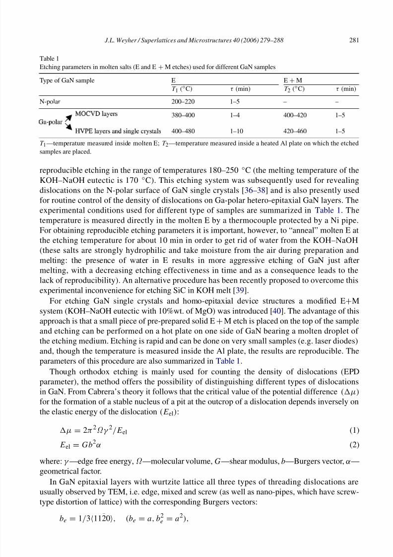
Superlattices and Microstructures 40 (2006) 279–288 www.elsevier.com/locate/superlattices Characterization of wide-band-gap semiconductors (GaN, SiC) by defect-selective etching and complementary methods J.L. Weyher ∗ Radboud University Nijmegen, Applied Materials Science, Toernooiveld 1, 6525 ED Nijmegen, The Netherlands Institute of High Pressure Physics, Polish Academy of Sciences, ul. Sokolowska 29/37, 01-142 Warsaw, Poland Received 9 May 2006; accepted 19 June 2006 Available online 8 August 2006 Abstract Two defect-selective etching approaches used for revealing and analysis of defects in wide-band-gap semiconductors (GaN, SiC) are described in detail: (i) orthodox etching in molten salts (KOH, NaOH) and hot acids (H 2 SO 4 , H 3 PO 4 ) and (ii) electroless photo-etching (photoelectrochemical or PEC) in aqueous solutions of KOH. Cha rac ter ist ic fea tur es of the se two tec hni ques, the ir rel iab ili ty and limita tion in re ve aling different types of defects (dislocations, stacking faults, micro-defects and electrically active chemical non- homogeneities) will be discussed. Examples of the use of both etching approaches to reveal defects in bulk and epitaxial layers of different crystallographic orientation are given. Numerous references to previous work on calibration of the etch features by means of TEM, X-ray diffraction, Raman and PL methods are cited. c 2006 Elsevier Ltd. All rights reserved. Keywords: Etching; Defects; Characterization; Semiconducting III–V materials 1. Introduction Def ect -se lec ti ve etc hing (DSE) pla ys an imp ortant role in str uct ural charac ter iza tio n of semiconductors. This method has several advantages over more sophisticated techniques such as Tr ansmission Ele ctr on Mic rosc opy (TEM), X-ra y dif fra cti on (XRD), Scanning Electron Microscopy-Cathodoluminescence (SEM-CL) or Electron Beam Induced Current (SEM-EBIC) ∗ Corre spon ding addr ess: Radbo ud Uni vers ity Nijme gen, Appli ed Mater ials Scienc e, T oernooiveld 1, 6525 ED Nijmegen, The Netherlands. Tel.: +31 24 3652586; fax: +31 24 3652620. E-mail address: [email protected] . 0749-6036/$ - see front matter c 2006 Elsevier Ltd. All rights reserved. doi:10.1016/j.spmi.2006.06.011
-
Upload
tri-minh-ta -
Category
Documents
-
view
220 -
download
0
Transcript of Char Act. of GaN SiC

8/7/2019 Char Act. of GaN SiC
http://slidepdf.com/reader/full/char-act-of-gan-sic 1/10

8/7/2019 Char Act. of GaN SiC
http://slidepdf.com/reader/full/char-act-of-gan-sic 2/10
8/7/2019 Char Act. of GaN SiC
http://slidepdf.com/reader/full/char-act-of-gan-sic 3/10

8/7/2019 Char Act. of GaN SiC
http://slidepdf.com/reader/full/char-act-of-gan-sic 4/10

8/7/2019 Char Act. of GaN SiC
http://slidepdf.com/reader/full/char-act-of-gan-sic 5/10

8/7/2019 Char Act. of GaN SiC
http://slidepdf.com/reader/full/char-act-of-gan-sic 6/10

8/7/2019 Char Act. of GaN SiC
http://slidepdf.com/reader/full/char-act-of-gan-sic 7/10

8/7/2019 Char Act. of GaN SiC
http://slidepdf.com/reader/full/char-act-of-gan-sic 8/10

8/7/2019 Char Act. of GaN SiC
http://slidepdf.com/reader/full/char-act-of-gan-sic 9/10

8/7/2019 Char Act. of GaN SiC
http://slidepdf.com/reader/full/char-act-of-gan-sic 10/10