Chapter5: DAC and ADC Part-II
27
Chapter5: DAC and ADC Part-II Asst.Prof.Dr.Supakit Nootyaskool
Transcript of Chapter5: DAC and ADC Part-II

Chapter5: DAC and ADC
Part-II
Asst.Prof.Dr.Supakit Nootyaskool

Objective
• To recognize mechanism of conversion from analog signal to digital signal, with digital circuit.
• To explain a R2R circuit to convert digital data to analog signal.
• To understand concept of convert analog signal to digital signal and digital to analog signal.
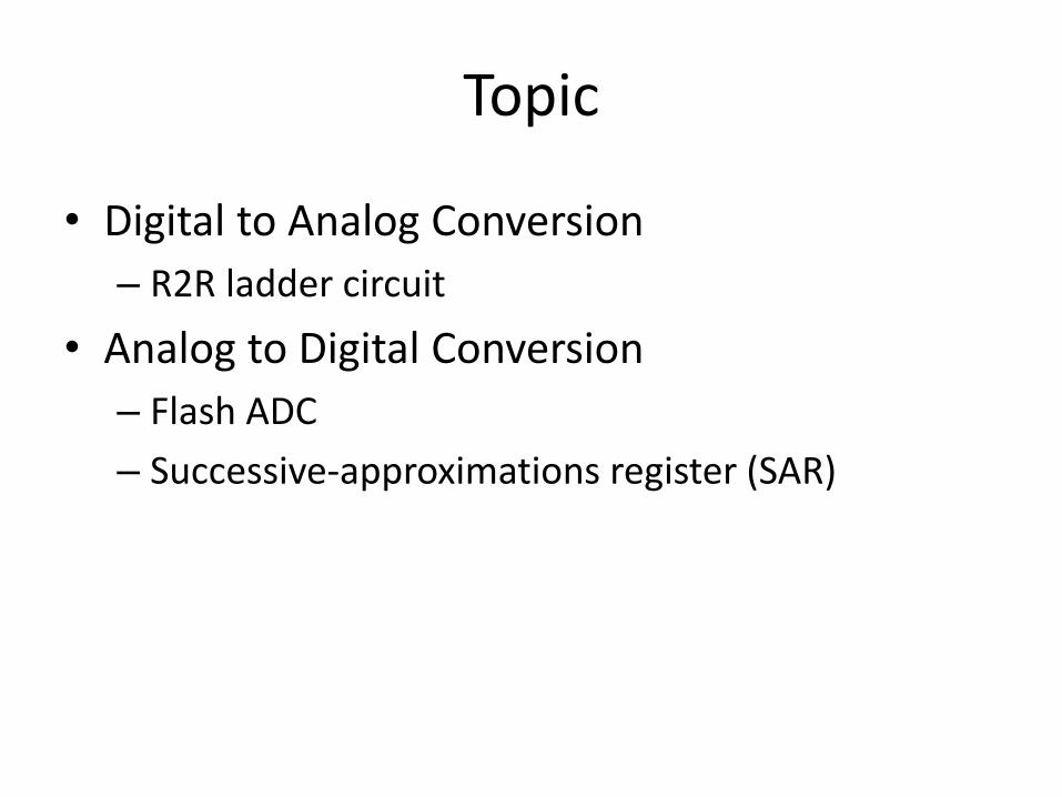
Topic
• Digital to Analog Conversion
– R2R ladder circuit
• Analog to Digital Conversion
– Flash ADC
– Successive-approximations register (SAR)

Overview

MP3 Signal Processor

Signal conversion concept
• DAC (Digital to Analog Conversion)
• ADC (Analog to Digital Conversion)
001100
110011
110001
111000
DAC
ADC
001100
110011
110001
111000

DIGITAL TO ANALOG CONVERSION

Example DAC design
Supposed
• 4-bits system
• Maximum output voltage at 12v

Example DAC design
Supposed
• 4-bits system
• Maximum output voltage at 12v
24 = 16 Levels (0 to 15)D0 D1 D2 D3
D3 D2 D1 D0 bitvalue Voltage
0 0 0 0 0 0
0 0 0 1 1 0.8
0 0 1 0 2 1.6
0 0 1 1 3 2.4
0 1 0 0 4 3.2
0 1 0 1 5 4
0 1 1 0 6 4.8
0 1 1 1 7 5.6
1 0 0 0 8 6.4
1 0 0 1 9 7.2
1 0 1 0 10 8
1 0 1 1 11 8.8
1 1 0 0 12 9.6
1 1 0 1 13 10.4
1 1 1 0 14 11.2
1 1 1 1 15 12

DAC: Resistance and voltage divider

DAC circuit (R2R)
R
2R
R
2R
R
2R
2R
2RD0
D1
D2
D3 Output+-

Opamp• Operational amplifiers is an IC amplifying a
small signal.
• Opamp has a very-high input impedance and having two input polarities (+) and (-).
• With input characteristic, Opamp uses for differential amplifier.

Opamp in the market• Famous IC code
– LM324
– LM741
– AD822

ANALOG TO DIGITAL CONVERSION

ADC circuits
• Characteristic of ADCs– Resolution
– Conversion speed
• Type of ADC circuit in the present– Flash ADC
– Pipelined ADC
– Successive Approximation Register
– Dual-slope convertor– Sigma-Delta converter

Flash ADC
• Serie resistor for voltage dividing to create voltage references
• Compare the voltage reference with an input voltage with Opamps.
• Use encoder circuit convert to BCD data.
• Strength– Very fast conversion
• Weakness– Number of comparator
require 2N-1
R
R
R
2R
+-
+-
+-
+-Vref
Vin
Encoder
Y0
Y1
Y2
Y3
D0
D1
D2
D3

Flash ADC: Example
4.9
1.225
2.45
3.675
2.8

Flash ADC: Example
4.9
1.225
2.45
3.675
2.8
2.8>1.225 1

Flash ADC: Encoder design
No. Y3 Y2 Y1 Y0 D2 D1 D0
0 0 0 0 0 0 0 0
1 0 0 0 1 0 0 1
2 0 0 1 1 0 1 0
3 0 1 1 1 0 1 1
4 1 1 1 1 1 0 0

Encoder design (added don’t care bits)
No. Y3 Y2 Y1 Y0 D2 D1 D0
0 0 0 0 0 0 0 0
1 0 0 0 1 0 0 1
2 0 0 1 1 0 1 0
3 0 1 1 1 0 1 1
4 1 1 1 1 1 0 0
5 1 X X X 1 0 0
6 1 X X X 1 0 0
7 1 X X X 1 0 0

Encoder design (SOP, K-MAP)

Flash ADC applied Arduino decoder

Successive Approximation Register
Key features
- Low energy.
- Interesting for digital circuit studying cause of having a counter, DAC, latch, and a comparator build to the system.

SAR-ADC

SAR-ADC: Example running
Control logic
CounterDAC
clock
Latcher
Up/Down clock
D0
D
3
Vcomp
D0
D
3
up
da
te
D0 D1 D2 D3
Vin
Vco
mp
comparator
D0 D1 D2 D3
6.4V
0V
+V
00
00
up

SAR-ADC: Example getting data
Control logic
CounterDAC
clock
Latcher
Up/Down clock
D0
D
3
Vcomp
D0
D
3
up
da
te
D0 D1 D2 D3
Vin
Vco
mp
comparator
D0 D1 D2 D3
6.4V
6.4V
0V
00
01
upupdatenoclock
0 0 0 1

ReferencesContent Links
Tutorial digital circuit https://www.tutorialspoint.com/digital_circuits/digital_circuits_conversion_of_flip_flops.htm
K-map online http://www.32x8.com/index.html
Encoder circuit design https://www.geeksforgeeks.org/encoder-in-digital-logic/
3bits flash ADC applied Arduino encoder
https://www.electronoobs.com/eng_circuitos_tut15_2.php
Flash ADC https://www.allaboutcircuits.com/textbook/digital/chpt-13/flash-adc/
Example ADC with simulation http://www.onmyphd.com/?p=analog.digital.converter#h3_resolution


![DAC&ADC [EngineeringDuniya.com]](https://static.fdocuments.in/doc/165x107/577cdcbb1a28ab9e78ab41f0/dacadc-engineeringduniyacom.jpg)