Chapter Testing Voltage Regulators 4 - · PDF fileTesting Voltage Regulators ... voltage...
59
Copyright © 2006 by Texas Instruments Inc. All rights reserved. 4-1 Testing Voltage Regulators Goals Understand the requirements for testing Voltage Regulator DC and AC parameters. Objectives Describe the procedure for testing line regulation. Describe the procedure for testing load regulation. In This Chapter DC Tests Line Regulation Load Regulation Standby Current Drain Output Short Circuit Minimum Load Current Drop–Out Voltage Adjust Pin Current AC Tests Voltage Start Up Output Noise Ripple Rejection Thermal Regulation Chapter 4
-
Upload
nguyenkiet -
Category
Documents
-
view
227 -
download
2
Transcript of Chapter Testing Voltage Regulators 4 - · PDF fileTesting Voltage Regulators ... voltage...

Copyright © 2006 by Texas Instruments Inc. All rights reserved.
4-1
Testing Voltage Regulators Goals Understand the requirements for testing Voltage Regulator DC and AC parameters. Objectives Describe the procedure for testing line regulation. Describe the procedure for testing load regulation. In This Chapter
DC Tests
Line Regulation Load Regulation Standby Current Drain Output Short Circuit Minimum Load Current Drop–Out Voltage Adjust Pin Current
AC Tests
Voltage Start Up Output Noise Ripple Rejection Thermal Regulation
Chapter 4

Copyright © 2006 by Texas Instruments Inc. All rights reserved.
4-2
A voltage regulator provides a constant voltage to the load under varying conditions of input level and output load.
Voltage
Regulator
Figure 4.11 xxxxxxx
A simple voltage regulator can be illustrated by two resistors.
Input OutputR1
R2
10V 5V
RL
R1
Figure 4.12 xxxxxxxxx
As long as the input voltage remains stable at 10 volts AND the load resistance RL does not change, the output voltage will remain at 5 volts.
? If the input voltage increases or decreases, then the resistor
ratio must change to continue the same output voltage level.
? If the output load increases or decreases, then resistor ratio must change to provide additional current.
? Resistor R2 dissipates more power than the load resistor.
Theoretical Voltage Regulators

Copyright © 2006 by Texas Instruments Inc. All rights reserved.
4-3
A practical voltage regulator includes three elements:
? Voltage reference
? Pass element
? Feedback control
Reference
Feedback
Input10V Pass Element
Load
Figure 4.13 Voltage regulator block diagram
The feedback element (op amp) compares the voltage delivered to the load with the reference voltage. The output of the feedback control drives the pass element (the NPN transistor). Any change in the input level or the output load is automatically sensed, and used to adjust the input of the pass element; which in turn causes the output level to remain stable.
Voltage Regulator Block Diagram
Copyright © 2006 by Texas Instruments Inc. All rights reserved.
4-4
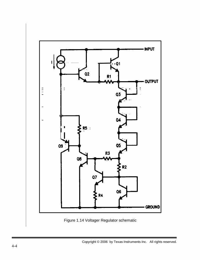
Figure 1.14 Voltager Regulator schematic

Copyright © 2006 by Texas Instruments Inc. All rights reserved.
4-5
Active voltage regulator circuits provide a stable output voltage with varying levels of input levels and output loads, with a minimum power requirement. A simplified schematic for a 5V regulator is shown in Figure 4.10. The emitter-base voltage of Q3, Q4, Q5 and Q8 provide the negative temperature coefficient component of the output voltage. This compensates for the positive temperature co-efficient of the output stage of Q1 and Q2. The voltage dropped across R3 provides a positive temperature-coefficient component. Q6 is operated at a much higher current density than Q7. This generates a voltage drop across R4 that tracks the emitter-base voltage differential of Q6 and Q7. The voltage drop across R3 is proportional to this differential, so a temperature-compensated output voltage can be obtained. In this circuit, Q8 is the gain stage providing regulation. The gain is increased by using a PNP transistor, Q9, as a buffer driving the active collector load from the current source. Q9 drives the output stage Q1 and Q2 which acts as the series pass element.
Transistor Level Circuit Description

Copyright © 2006 by Texas Instruments Inc. All rights reserved.
4-6
Line Regulation: A 20 volt change on the input level causes an output level change of less than 30mV. Load Regulation: A change in the load current from zero to the maximum rated output will cause the output voltage to drop by less than 20mV. Maximum Power Dissipation: Voltage regulators are available with device power dissipation ranges from 100mA for low power applications, up to 3 amps and more for high power requirements. Low Dropout Voltage: Regulators function with an input level several volts greater than the regulated output level. A typical 5 volt regulator needs only 6 or 7 volts on the input to function properly. Specially designed regulators have drop-out voltages of 0.5 volts. Input Voltage Range: The range of DC input voltages for a typical regulator ranges from 2 volts to more than 20 volts over the output level. A 5 volt regulator can operate with an input level from 7 volts to 25 volts.
Output Noise Voltage: The RMS ac voltage at the output with constant load is typically less than 20uV from 10Hz to 100kHz. Quiescent Current: The amount of current used by the regulator (not delivered to the load) is less than 5mA for a 1.0 Amp regulator. Ripple Rejection: The rejection of AC components on the input to the output is typically a 1000:1 ratio. A 1 volt 60Hz component on the input would create only 1mV of ripple on the output. Thermal Regulation: The device temperature can vary by over 100 degrees Centigrade with less than 5mV change on the output voltage. Short Circuit and Over Current Protection: The device protects itself from damage from a short circuit on the output, or excessive load current.
Voltage Regulator Features

Copyright © 2006 by Texas Instruments Inc. All rights reserved.
4-7
OUTIN
IN
COM
OUT
Figure 4.15 Fixed Voltage Regulator
IN OUT
IN
COM
OUT
R2
R1
Figure 4.16 Adjustable Voltage Regulator
Voltage Regulator Features (continued)

Copyright © 2006 by Texas Instruments Inc. All rights reserved.
4-8
Output Voltage (V0UT). The regulated voltage at the output of the voltage regulator referenced to the external zero reference level of the supply voltage (ground or adjust pin as specified). Supply Voltage (VLINE). The voltage supplied at the input of the voltage regulator. Input Voltage Range The range of input supply voltage level over which the regulator will operate. Output Voltage Range The range of output voltage over which the regulator will operate. Line Regulation (VRLINE) The change in output voltage for a specified change in input voltage under a constant load condition. Load Regulation (VRLOAD) The change in output voltage for a specified change in the load current under a constant input voltage. Output Short Circuit Current (IOS) The current from the output of the voltage regulator when the output is at zero volts (ground). For Fixed Voltage Regulators only: Standby Current Drain (ISCD) The supply current drawn by the regulator with no load or with a specified high resistance load. This parameter applies to fixed regulators only. For Adjustable Voltage Regulators only: Minimum Load Current (IMIN) The minimum current at which the voltage regulator will regulate the output voltage. This parameter applies to adjustable regulators only. Adjust Pin Current (IADJ) The current required at the adjust pin of adjustable voltage regulators.
Voltage Regulator DC Tests Fixed and Adjustable

Copyright © 2006 by Texas Instruments Inc. All rights reserved.
4-9
Figure 4.15 Voltage Regulator Test Circuit With Power and Sense Lines
Copyright © 2006 by Texas Instruments Inc. All rights reserved.
4-10
Test Circuit Description
DC Voltmeter (VM1) measures the output voltage of the DUT. The voltmeter must be programmable to make a measurement at a specific interval after the changes in line voltage or load current for the DUT response time tests. DC Current Meter (CM1) measures output short circuit current DC Current Meter (CM2) measures standby or adjustment current. AC Voltmeter (VM2) is used to measure DUT noise voltage and ripple. Input Voltage Supply (VS1) forces positive or negative voltage to the DUT input. The supply must be able to generate a voltage pulse for the DUT response time tests. Standby Voltage Supply (VS2) forces positive or negative voltage to the ground reference of the DUT. The standby voltage supply should have separate voltage sense and power connections. Output Voltage Supply (VS3) simulates a momentary short circuit at the DUT output. Output Current Supply (CS) sources or sinks current to the DUT. The output current supply must be able to generate a current pulse of amplitude and width for measurement of DUT load regulation.
Copyright © 2006 by Texas Instruments Inc. All rights reserved.
4-11
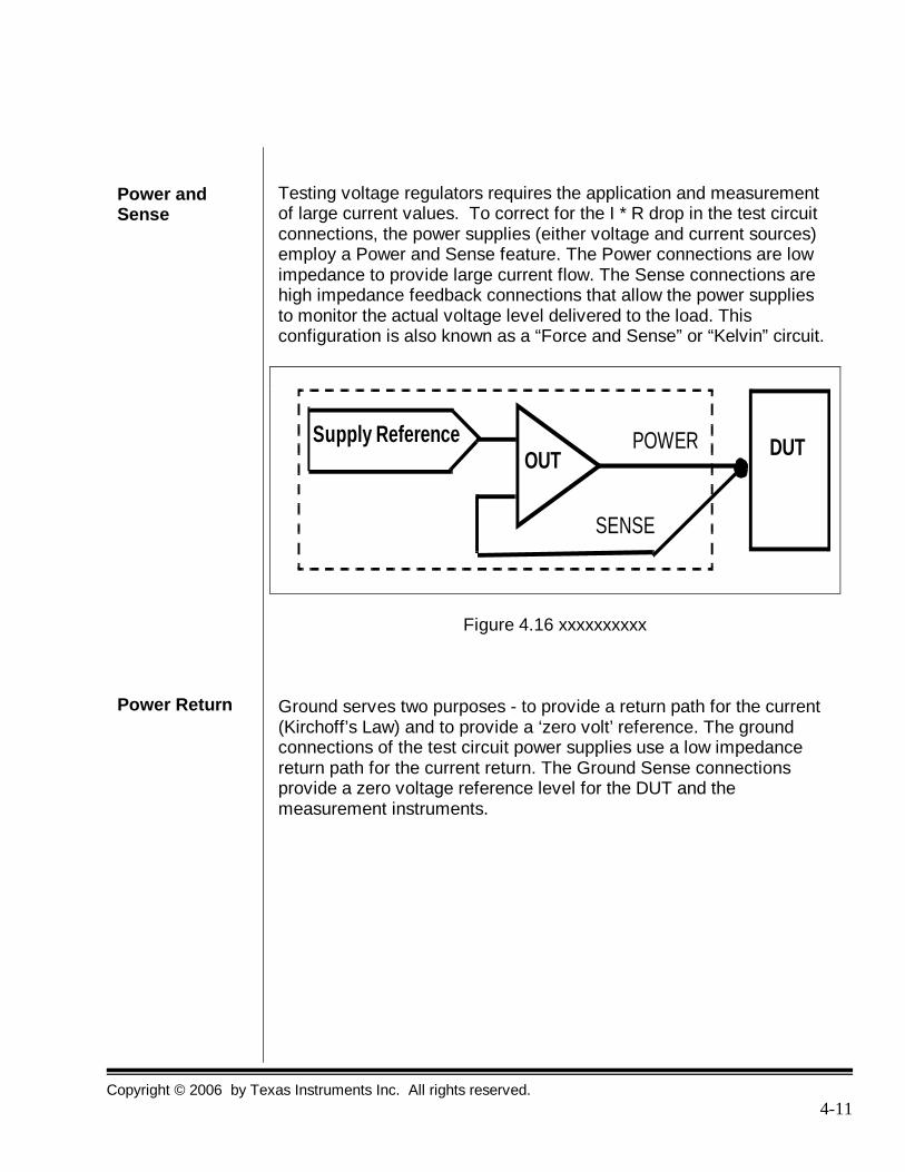
Testing voltage regulators requires the application and measurement of large current values. To correct for the I * R drop in the test circuit connections, the power supplies (either voltage and current sources) employ a Power and Sense feature. The Power connections are low impedance to provide large current flow. The Sense connections are high impedance feedback connections that allow the power supplies to monitor the actual voltage level delivered to the load. This configuration is also known as a “Force and Sense” or “Kelvin” circuit.
POWER Supply ReferenceOUT DUT
SENSE
Figure 4.16 xxxxxxxxxx
Ground serves two purposes - to provide a return path for the current (Kirchoff’s Law) and to provide a ‘zero volt’ reference. The ground connections of the test circuit power supplies use a low impedance return path for the current return. The Ground Sense connections provide a zero voltage reference level for the DUT and the measurement instruments.
Power and Sense Power Return

Copyright © 2006 by Texas Instruments Inc. All rights reserved.
4-12
S2
C11uF
S1
+
-
VS30V
DC~ANO DATA CM2
AC VNO DATA
VM2 (AC)
Is1100mA
DC~VNO DATA
VM1
DC~ANO DATA CM1
+
-
VS20V
IN
COM
OUT
U1
+
-
VS110V
RL
Figure 4.17 Circuit Simulator Version of the Test Circuit
Copyright © 2006 by Texas Instruments Inc. All rights reserved.
4-13
S2
C11uF
S1
+
-
VS30V
DC~A 0.000 A CM2
AC V 21.78pV
VM2 (AC)
Is1100mA
DC~V 5.028 V
VM1
DC~A-3.879mACM1
+
-
VS20V
IN
COM
OUT
U1
+
-
VS110V
RL
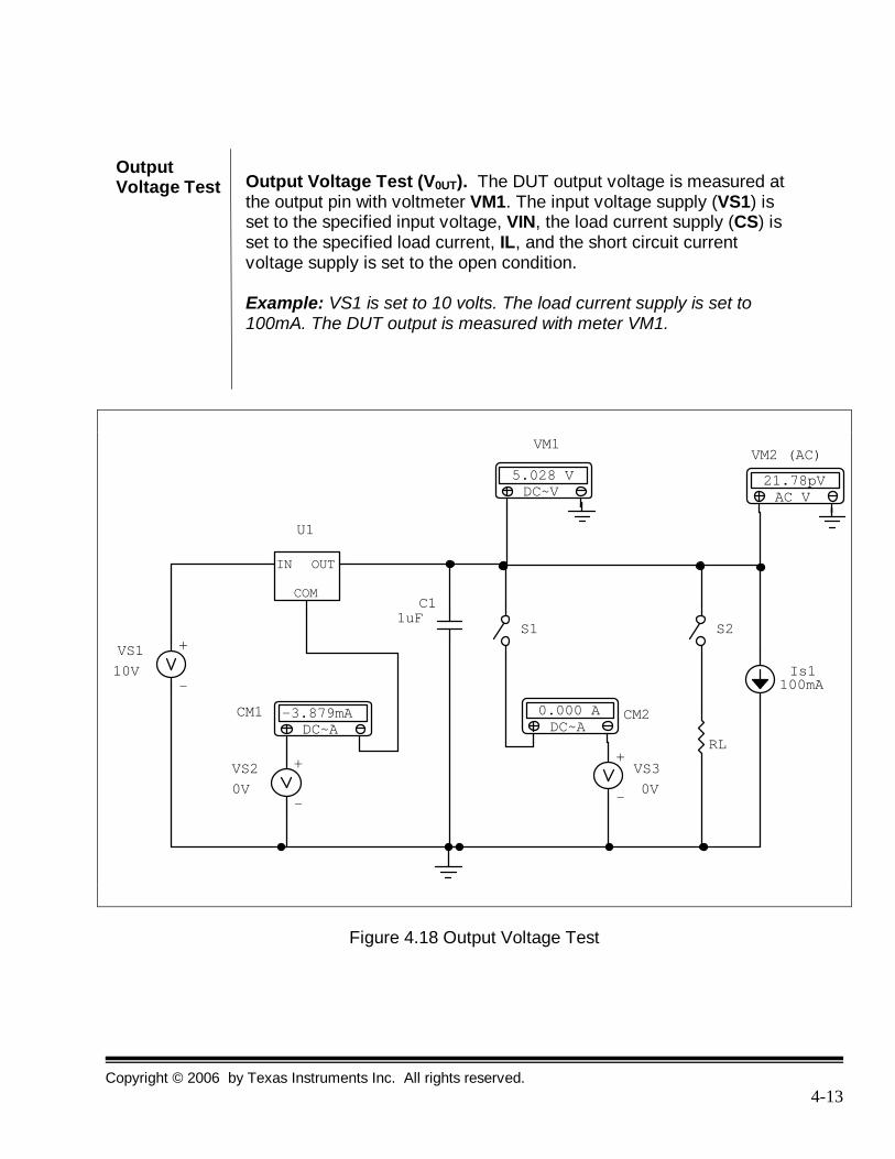
Figure 4.18 Output Voltage Test
Output Voltage Test (V0UT). The DUT output voltage is measured at the output pin with voltmeter VM1. The input voltage supply (VS1) is set to the specified input voltage, VIN, the load current supply (CS) is set to the specified load current, IL, and the short circuit current voltage supply is set to the open condition. Example: VS1 is set to 10 volts. The load current supply is set to 100mA. The DUT output is measured with meter VM1.
Output Voltage Test

Copyright © 2006 by Texas Instruments Inc. All rights reserved.
4-14
Figure 4.19 Load Regulation Test
Load Regulation
Load Regulation (VRLOAD) measures the change in output voltage for a specified change in the load current under a constant input voltage. Load regulation is tested by making two measurements of VOUT at two different values of load current. Vout is measured (E2) at an initial load current, IL1. The load current supply is then switched to a value IL2 and the output voltage is measured again (E3) at a specified time after the current transition. Load regulation is calculated as:
VRLOAD = E3 - E2 Example: VS1 is set to 10 volts. The load current supply is set to 10mA. The DUT output is measured with meter VM1, and reads 5.01 volts (E2). Then the load current supply is set to 150mA. The DUT output is measured again, and reads 5.21 volts (E3). The VRLOAD value is therefore 5.028v – 4.958v = 80mV.
S2
C11uF
S1
+
-
VS30V
DC~A 0.000 A CM2
AC V 21.69pV
VM2 (AC)
Is1150mA
DC~V 4.948 V
VM1
DC~A-3.827mACM1
+
-
VS20V
IN
COM
OUT
U1
+
-
VS110V
RL
A

Copyright © 2006 by Texas Instruments Inc. All rights reserved.
4-15
Figure 4.19 Standby Current Drain (Quiescent Current) Test
Standby Current Drain
Standby Current Drain (ISCD) is supply current drawn by the regulator with no load or with a specified high resistance load Standby current is measured at the control pin output with current meter CM1. Line voltage and load current are set to the specified levels and the standby current voltage supply is set to maintain the control pin voltage level at the ground reference level of the regulator in test. Example: The load current supply (CS) is set to 100mA, and the input level (VS1) is set to 10.0 volts. The standby voltage reference (VS3) is set to 0.0 volts. The standby current is measured at 3.879 mA.
S2
C11uF
S1
+
-
VS30V
DC~A 0.000 A CM2
AC V 21.78pV
VM2 (AC)
Is1100mA
DC~V 5.028 V
VM1
DC~A-3.879mACM1
+
-
VS20V
IN
COM
OUT
U1
+
-
VS110V
RL
Copyright © 2006 by Texas Instruments Inc. All rights reserved.
4-16
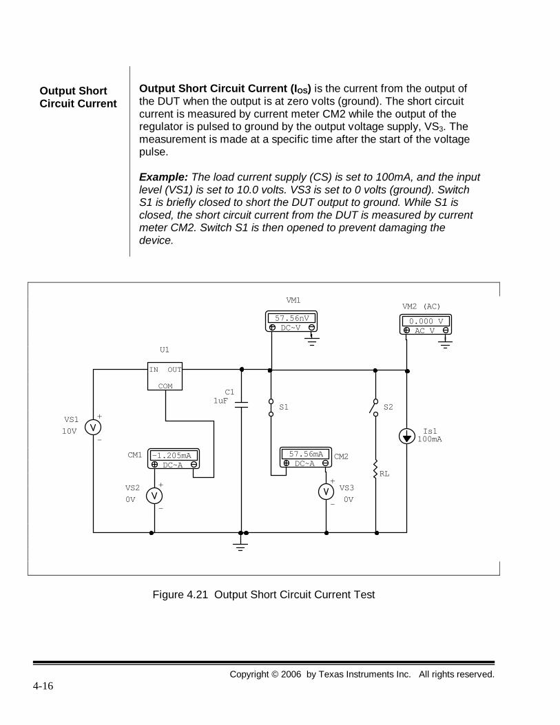
Figure 4.21 Output Short Circuit Current Test
Output Short Circuit Current (IOS) is the current from the output of the DUT when the output is at zero volts (ground). The short circuit current is measured by current meter CM2 while the output of the regulator is pulsed to ground by the output voltage supply, VS3. The measurement is made at a specific time after the start of the voltage pulse. Example: The load current supply (CS) is set to 100mA, and the input level (VS1) is set to 10.0 volts. VS3 is set to 0 volts (ground). Switch S1 is briefly closed to short the DUT output to ground. While S1 is closed, the short circuit current from the DUT is measured by current meter CM2. Switch S1 is then opened to prevent damaging the device.
Output Short Circuit Current
S2
C11uF
S1
+
-
VS30V
DC~A 57.56mA CM2
AC V 0.000 V
VM2 (AC)
Is1100mA
DC~V 57.56nV
VM1
DC~A-1.205mACM1
+
-
VS20V
IN
COM
OUT
U1
+
-
VS110V
RL

Copyright © 2006 by Texas Instruments Inc. All rights reserved.
4-17
VM1
CM1
CM2
Voltage RegulatorTest Circuit
VM2
CSVS1
VS2
(Current Supply)
VS3
DUT
S2
RL
AC VNO DATA
C1
1uFS1
IN
COM
OUT
DC ANO DATA
DC ANO DATA
DC VNO DATA
+
-
0V
+
-
0V
+
-
10V
100mA
Figure 4.21 Voltage Start-Up Test
Voltage Start-up (VSTART) is voltage at the output of the regulator after a step in input voltage from zero volts to a nominal input voltage. Start-up voltage is measured at the output of the regulator by voltmeter VM1. The input voltage supply, VS1, is switched from zero volts to a specified value of VIN and the output voltage is measured at a specified time, T1, after the initiation of the input voltage transition. A load resistor RL, is programmed to a specified value and the control/adjustment pin is biased as specified by either the voltage supply, VS2. or the divider, VD.
Example: The output current source CS is open. Switch S2 is closed to connect load resistor RL. At the beginning of the test, input supply VS1 is programmed to 0 volts. Then VS1 is programmed to 10.0 volts, and the DUT output response is measured at time T1.
Voltage Start-up

Copyright © 2006 by Texas Instruments Inc. All rights reserved.
4-18
Figure 4.22 Thermal Regulation Test
Thermal Regulation (VRTH) is change in output voltage at a specified input voltage after increasing the load current from minimum to a specified value and waiting a specified time. The change in output voltage is due to thermal effects and is specified as a function of power dissipation in the DUT. The output load current is set to specified load current. Output voltages V1 and V2 are then measured at specified times T1 and T2. Example: The load current supply (CS) is set to 100mA, and the input level (VS1) is set to 10.0 volts. VS3 is set to 0 volts (ground). The DUT output is measured with meter VM1 (E9) at time T1, with a value of 5.12 volts. After 5 seconds, (time T2), the output of the DUT is measured again (E10), a value of 5.17 volts. The thermal regulation is calculated as E10 - E9, or 5mV.
Thermal Regulation
VM1
CM1
CM2
Voltage RegulatorTest Circuit
VM2
CSVS1
VS2
(Current Supply)
VS3
DUT
S2
RL
AC VNO DATA
C1
1uFS1
IN
COM
OUT
DC ANO DATA
DC ANO DATA
DC VNO DATA
+
-
0V
+
-
0V
+
-
10V
100mA

Copyright © 2006 by Texas Instruments Inc. All rights reserved.
4-19
Figure 4.21 Adjustable Voltage Regulator Test Circuit
DC Tests - For Adjustable Voltage Regulators The test circuit for adjustable voltage regulators includes a programmable voltage divider (VD), illustrated by resistors R1 and R2.
Adjustable Voltage Regulators
CurrentSupply
DCVM1
ACVM2
CS
CM2
VS1
VS3
DUT
Adjustable Voltage RegulatorTest Circuit
Switch S1 is normally open.Closing S1 shorts the DUT to ground
Switch S3A is normally closed. Switch S3B is normally open.
CM1
100mA
DC A 0.000 A
S3B
S3AS2
AC V 422.0nV
C1
1uF S1
IN
COM
OUT
DC A 0.000 A
DC V 12.19 V
+
-
0V
+
-
20V
R22000
R1240
RL

Copyright © 2006 by Texas Instruments Inc. All rights reserved.
4-20
Figure 4.22 Minimum Load Current Test
Minimum Load Current (IMIN) is the minimum current at which the voltage regulator will regulate the output voltage. The current load source (CS) is programmed to the specified minimum load current. Supply VS1 is set to a nominal level, and the load resistor is opened. The output of the DUT is measured and tested against limits. Example: (12 volt regulator). The load current supply (CS) is set to the specified minimum current load of 10mA. The input level (VS1) is set to 20.0 volts, and switch S2 is opened to disconnect load resistor RL. The output voltage of the DUT is measured and tested against specified limits.
Minimum Load Current
CurrentSupply
DCVM1
ACVM2
CS
CM2
VS1
VS3
DUT
Adjustable Voltage RegulatorTest Circuit
Switch S1 is normally open.Closing S1 shorts the DUT to ground
Switch S3A is normally closed. Switch S3B is normally open.
CM1
100mA
DC A 0.000 A
S3B
S3AS2
AC V 422.0nV
C1
1uF S1
IN
COM
OUT
DC A 0.000 A
DC V 12.19 V
+
-
0V
+
-
20V
R22000
R1240
RL

Copyright © 2006 by Texas Instruments Inc. All rights reserved.
4-21
Adjust Pin Current (IADJ) is current required at the adjust pin of adjustable voltage regulators. The current is measured at the adjust pin with current meter CM1. For this measurement the voltage divider, VD, is disconnected from the output of the DUT by programming resistor R1 to be open. Line voltage (VS1) and load current (CS) are set to specified voltages and the standby current voltage supply is set to maintain the adjust pin voltage level at ground. Example: Supply VS1 is set to 20v. Current load supply CS is set to 100mA. The divider circuit R1/R2 is disconnected from the output of the DUT. The IADJ current is measured by current meter CM1.
Adjust Pin Current
CurrentSupply
DCVM1
ACVM2
CS
CM2
VS1
VS3
DUT
Adjustable Voltage RegulatorTest Circuit
Switch S1 is normally open.Closing S1 shorts the DUT to ground
Switch S3A is normally closed. Switch S3B is normally open.
CM1
100mA
DC A-48.24uA
S3B
S3A S2
AC V 4.327nV
C1
1uF S1
IN
COM
OUT
DC A 0.000 A
DC V 1.298 V
+
-
0V
+
-
20V
R22000
R1240
RL
Figure 4.23 Adjust Pin Current Test Circuit

Copyright © 2006 by Texas Instruments Inc. All rights reserved.
4-22
Figure 4.24 xxxxxxxxxxxxxxx
Thermal Regulation (VRTH) is change in output voltage at a specified input voltage after increasing the load current from minimum to a specified value and waiting a specified time. The change in output voltage is due to thermal effects and is specified as a function of power dissipation in the DUT. The output load current is set to specified load current. Output voltages V1 and V2 are then measured at specified times T1 and T2. Example: The load current supply (CS) is set to 100mA, and the input level (VS1) is set to 10.0 volts. VS3 is set to 0 volts (ground). The DUT output is measured with meter VM1 (E9) at time T1, with a value of 5.12 volts. After 5 seconds, (time T2), the output of the DUT is measured again (E10), a value of 5.17 volts. The thermal regulation is calculated as E10 - E9, or 5mV.
Thermal Regulation
CurrentSupply
DCVM1
ACVM2
CS
CM2
VS1
VS3
DUT
Adjustable Voltage RegulatorTest Circuit
Switch S1 is normally open.Closing S1 shorts the DUT to ground
Switch S3A is normally closed. Switch S3B is normally open.
CM1
100mA
DC A 0.000 A
S3B
S3AS2
AC V 422.0nV
C1
1uF S1
IN
COM
OUT
DC A 0.000 A
DC V 12.19 V
+
-
0V
+
-
20V
R22000
R1240
RL

Copyright © 2006 by Texas Instruments Inc. All rights reserved.
4-23
Figure 4.26 Drop-Out Test Circuit
Drop-out describes the minimum difference between the input level and the output level that is required for the voltage regulator to properly function. Testing low-dropout regulators (LDO) requires that the input voltage be programmed to a level slightly above the normal regulator output level. Example: A 5.0 volt regulator with a 100mV drop-out specification: Step One: Measure the output voltage under nominal conditions (VIN = 10 V) Step Two: Program the input voltage level to the measured output voltage level plus the drop-out (VOUT + Drop-Out) and test the DUT output again.
Low Dropout Tests
S2
C11uF
S1
+
-
VS30V
DC~A 0.000 A CM2
AC V 21.78pV
VM2 (AC)
Is1100mA
DC~V 5.028 V
VM1
DC~A-3.879mACM1
+
-
VS20V
IN
COM
OUT
U1
+
-
VS15.128
RL
+
-
VS15.128

Copyright © 2006 by Texas Instruments Inc. All rights reserved.
4-24
0 833u 1.67m 2.5m 3.33m 4.17m 5m5.04
5.04
5.04
5.04
5.04
5.04
5.04
Xa: 5.000m Xb: 0.000 Yc: 5.036 Yd: 5.036
a-b: 5.000mc-d: 206.7p
freq: 200.0
Ref=Ground X=time(S) Y=voltage
d
cb a
A
Figure 4.27 Output Noise Test Circuit
Figure 4.28 Output Noise across 5mS
Noise Output (N0) is the RMS noise voltage output from the regulator for a specified DC input voltage. The test specification includes the use of the input capacitor C2, and output filter capacitor C1. With the specified voltage applied to the input of the regulator, the RMS noise voltage is measured with AC voltmeter VM2 (which has a specified bandwidth). Example: Supply VS1 is set to 20v. Current load supply CS is set to 100mA. The RMS output is measured with AC meter VM2 at 21.78 pico volts.
Noise Output
C2
S2
C1
S1
+
-
VS30V
DC~A 0.000 A CM2
AC V 21.78pV
VM2 (AC)
Is1100mA
DC~V 5.028 V
VM1
DC~A-3.879mACM1
+
-
VS20V
IN
COM
OUT
U1
+
-
VS110
RL
Copyright © 2006 by Texas Instruments Inc. All rights reserved.
4-25
0 13.9m 27.8m 41.7m 55.6m 69.4m 83.3m0
2
4
6
8
10
12
Xa: 83.33m Xb: 0.000 Yc: 10.00 Yd: 0.000
a-b: 83.33mc-d: 10.00
freq: 12.00
X: 0.000 Offsets Y: 0.000 Offsets
Ref=Ground X=time(S) Y=voltage
d
c
b aAB
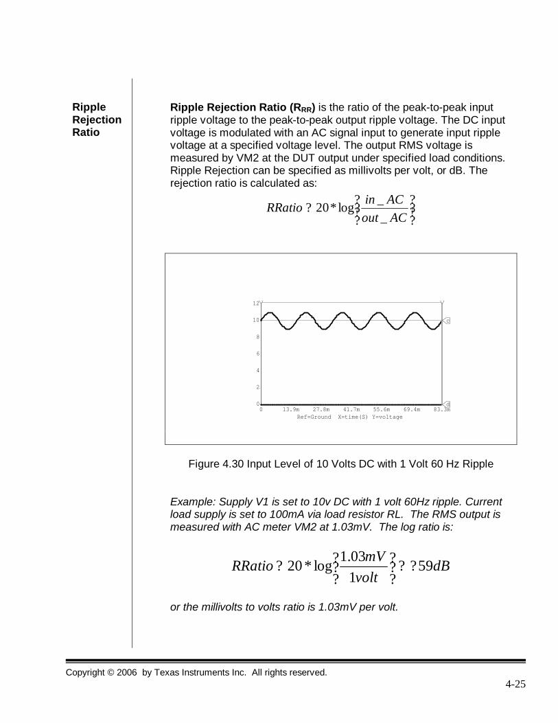
Ripple Rejection Ratio
Ripple Rejection Ratio (RRR) is the ratio of the peak-to-peak input ripple voltage to the peak-to-peak output ripple voltage. The DC input voltage is modulated with an AC signal input to generate input ripple voltage at a specified voltage level. The output RMS voltage is measured by VM2 at the DUT output under specified load conditions. Ripple Rejection can be specified as millivolts per volt, or dB. The rejection ratio is calculated as:
????
?????
ACoutACinRRatio
__log*20
0 13.9m 27.8m 41.7m 55.6m 69.4m 83.3m0
2
4
6
8
10
12
Xa: 83.33m Xb: 0.000 Yc: 10.00 Yd: 0.000
a-b: 83.33mc-d: 10.00
freq: 12.00
X: 0.000 Offsets Y: 0.000 Offsets
Ref=Ground X=time(S) Y=voltage
d
c
b aAB
Figure 4.30 Input Level of 10 Volts DC with 1 Volt 60 Hz Ripple Example: Supply V1 is set to 10v DC with 1 volt 60Hz ripple. Current load supply is set to 100mA via load resistor RL. The RMS output is measured with AC meter VM2 at 1.03mV. The log ratio is:
dBvolt
mVRRatio 59
103.1
log*20 ??????
???
or the millivolts to volts ratio is 1.03mV per volt.

Copyright © 2006 by Texas Instruments Inc. All rights reserved.
4-26
Copyright © 2006 by Texas Instruments Inc. All rights reserved.
4-27
Chapter Four Testing Voltage Regulators
Knowledge Check
1. Sketch the test circuit for testing DC line regulation and DC load regulation. 2. Describe the procedure for testing line regulation. 3. Describe the procedure for testing load regulation.

Copyright © 2006 by Texas Instruments Inc. All rights reserved.
4-28

Copyright © 2006 by Texas Instruments Inc. All rights reserved.
4-29

Copyright © 2006 by Texas Instruments Inc. All rights reserved.
4-30

Copyright © 2006 by Texas Instruments Inc. All rights reserved.
4-31

Copyright © 2006 by Texas Instruments Inc. All rights reserved.
4-32

Copyright © 2006 by Texas Instruments Inc. All rights reserved.
4-33

Copyright © 2006 by Texas Instruments Inc. All rights reserved.
4-34

Copyright © 2006 by Texas Instruments Inc. All rights reserved.
4-35

Copyright © 2006 by Texas Instruments Inc. All rights reserved.
4-36
Copyright © 2006 by Texas Instruments Inc. All rights reserved.
4-37

Copyright © 2006 by Texas Instruments Inc. All rights reserved.
4-38

Copyright © 2006 by Texas Instruments Inc. All rights reserved.
4-39

Copyright © 2006 by Texas Instruments Inc. All rights reserved.
4-40
Copyright © 2006 by Texas Instruments Inc. All rights reserved.
4-41

Copyright © 2006 by Texas Instruments Inc. All rights reserved.
4-42

Copyright © 2006 by Texas Instruments Inc. All rights reserved.
4-43

Copyright © 2006 by Texas Instruments Inc. All rights reserved.
4-44

Copyright © 2006 by Texas Instruments Inc. All rights reserved.
4-45
Copyright © 2006 by Texas Instruments Inc. All rights reserved.
4-46

Copyright © 2006 by Texas Instruments Inc. All rights reserved.
4-47

Copyright © 2006 by Texas Instruments Inc. All rights reserved.
4-48

Copyright © 2006 by Texas Instruments Inc. All rights reserved.
4-49

Copyright © 2006 by Texas Instruments Inc. All rights reserved.
4-50

Copyright © 2006 by Texas Instruments Inc. All rights reserved.
4-51

Copyright © 2006 by Texas Instruments Inc. All rights reserved.
4-52

Copyright © 2006 by Texas Instruments Inc. All rights reserved.
4-53

Copyright © 2006 by Texas Instruments Inc. All rights reserved.
4-54

Copyright © 2006 by Texas Instruments Inc. All rights reserved.
4-55

Copyright © 2006 by Texas Instruments Inc. All rights reserved.
4-56

Copyright © 2006 by Texas Instruments Inc. All rights reserved.
4-57

Copyright © 2006 by Texas Instruments Inc. All rights reserved.
4-58

Copyright © 2006 by Texas Instruments Inc. All rights reserved.
4-59