Chapter 8 Oscillators - SJTUiwct.sjtu.edu.cn/personal/xygan/Chapter 8 Oscillators-2019.pdf ·...
32
1 Chapter 8 Oscillators
Transcript of Chapter 8 Oscillators - SJTUiwct.sjtu.edu.cn/personal/xygan/Chapter 8 Oscillators-2019.pdf ·...
1
Chapter 8 Oscillators
2
Sections to be covered
• 8.2 Basic Principles• 8.3 Cross-Coupled Oscillator• 8.4 Three-Point Oscillators• 8.5 Voltage-Controlled Oscillators

3
Chapter Outline
General Principles
Feedback View One-Port View Cross-Coupled Oscillator Three-Point Oscillators

4
Feedback View of Oscillators
An oscillator may be viewed as a “badly-designed” negative-feedback amplifier—so badly designed that it has a zero or negative phase margin.
What happens if at a sinusoidal frequency, ω1, H(s=jω1)becomes equal to -1? The gain from the input to the output goes to infinity, allowing the circuit to amplify a noise component at ω1
That is, the circuit can sustain an output at ω1.

5
Barkhausen’s Criteria
For the circuit to reach steady state, the signal returning to A must exactly coincide with the signal that started at A. We call ∠ H(jω1) a “frequency-dependent” phase shift to distinguish it from
the 180 ° phase due to negative feedback. H(s) contributes an additional phase shift of 180 ° at ω1, thereby creating
positive feedback at this frequency.
H(jω1) = -1
(a) 1800 frequency-dependent phase shift due to H(s) (b) 3600 total phase shift.

6
Significance of |H(jw1)| = 1
For a noise component at ω1 to “build up” as it circulates around the loop with positive feedback, the loop gain must be at least unity.
We call |H(jω1)| > 1 the “startup” condition.(起振条件)
The growth shown in figure above still occurs but at a faster rate because the returning waveform is amplified by the loop.
The amplitude growth eventually ceases due to circuit nonlinearities.
An input at ω1 propagates through H(s), emerging unattenuated but inverted.
The result is subtracted from the input, yielding a waveform with twice the amplitude.
This growth continues with time.

7
Tuned OscillatorWe wish to build a negative-feedback oscillatory system using “LC-tuned” amplifier stages. Let us examine the frequency response of the stage:
At very low frequencies, L1dominates the load and
|Vout/Vin| is very small and ∠(Vout/Vin) remains around -90°
At the resonance frequency ω0, the tank reduces to Rp
The phase shift from the input to the output is thus equal to 180°
At very high frequencies, C1 dominates
|Vout/Vin| dinimishes∠(Vout/Vin) approaches +90°
Can the circuit oscillate if its input and output are shorted?
No!!!!!!
No frequency satisfies Barkhausen’s criteria;
The total phase shift fails to reach 3600 at any frequency.

8
Cascade of Two Tuned Amplifiers in Feedback Loop The circuit provides a phase shift of 180 ° with possibly adequate gain (gmRp)
at ω0. We need to increase the phase shift to 360 °, perhaps by inserting another
stage in the loop. The idea is to cascade two identical LC-tuned stages so that, at resonance, the
total phase shift around the loop is equal to 3600.
The circuit oscillates if the loop gain is equal to or greater than unity:

9
Cross-Coupled Oscillator
The oscillator above suffers from poorly-defined bias currents. The circuit below is more robust and can be viewed as an inductively-loaded differential pair with positive feedback.
Compute the voltage swings if M1 and M2experience complete current switching with abrupt edges. (refer to Example 8.7)
10
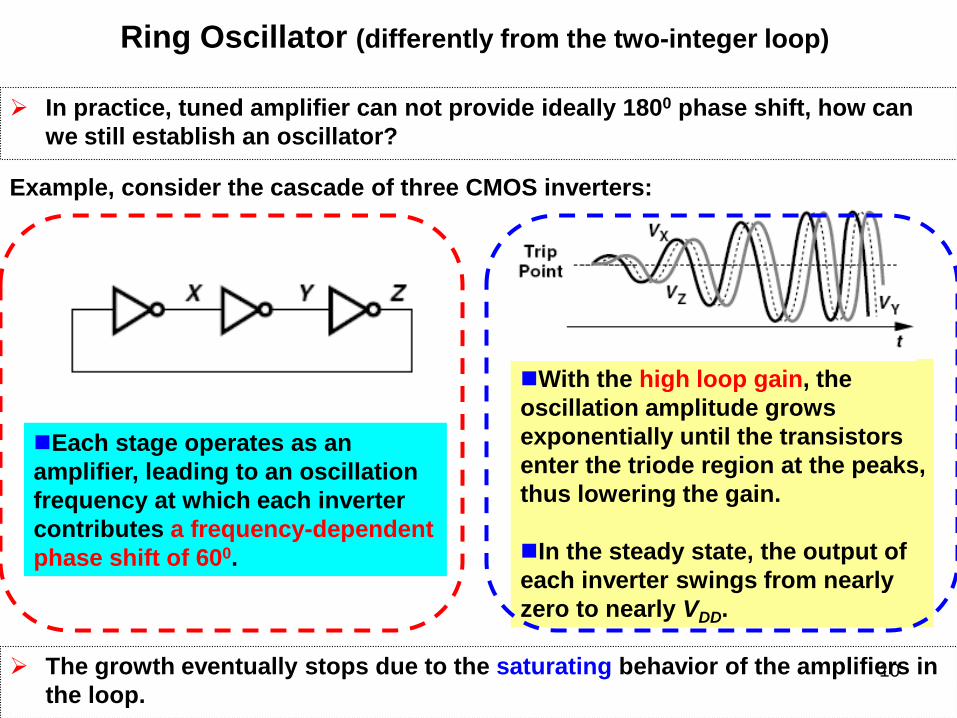
Ring Oscillator (differently from the two-integer loop)
In practice, tuned amplifier can not provide ideally 1800 phase shift, how can we still establish an oscillator?
Example, consider the cascade of three CMOS inverters:
Each stage operates as an amplifier, leading to an oscillation frequency at which each inverter contributes a frequency-dependent phase shift of 600.
With the high loop gain, the oscillation amplitude grows exponentially until the transistors enter the triode region at the peaks, thus lowering the gain.
In the steady state, the output of each inverter swings from nearly zero to nearly VDD.
The growth eventually stops due to the saturating behavior of the amplifiers in the loop.

11
One-Port View of Oscillators An alternative perspective views oscillators as two one-port components,
a lossy resonator an active circuit that cancels the loss.
Let us assume a lossy tank. Such a circuit behaves similarly except that Rpdrains and “burns” some of the capacitor energy in every cycle, causing an exponential decay in the amplitude.
If an active circuit supply the energy lost in each period, then the oscillation can be sustained.
An active circuit exhibiting an input resistance of -Rp can be attached across the tank to cancel the effect of Rp. Recreating the ideal lossless scenario.
A current impulse, I0δ(t), is applied to a lossless tank.
The impulse is entirely absorbed by C1, generating a voltage of I0/C1. The charge on C1 then begins to flow through L1, and the output voltage falls.
When Vout reaches zero, C1 carries no energy but L1 has a current equal to L1dVout /dt, which charges C1 in the opposite direction, driving Vouttoward its negative peak.
This periodic exchange of energy between C1 and L1 continues indefinitely, with an amplitude given by the strength of the initial impulse.
exponential decay

12
How Can a Circuit Present a Negative Input Resistance?
The negative resistance varies with frequency.
Zin=
Negative resistance

13
Connection of Lossy Inductor to Negative-Resistance Circuit
Since the capacitive component in equation above can become part of the tank, we simply connect an inductor to the negative-resistance port.
The circuit oscillates if:
Express the oscillation condition in terms of inductor’s parallel equivalent resistance, Rp, rather than RS.
The startup condition:if Q>3, the series combination can be transformed to a parallel combination:
For oscillation to occur, the transistor must provide sufficient “strength” (transconductance). gmRp ≥4. (The minimum allowable gm is obtained if C1 =C2.)

14
Three-Point Oscillators (1)
Three different oscillator topologies can be obtained by grounding each of the transistor terminals.
If C1 = C2, the transistor must provide sufficient transconductance to satisfy
According to the one-port view of oscillators, a negative resistance is expected:
Colpitts oscillator, gate grounded
Clapp oscillator, drain grounded
source grounded

15
Three-Point Oscillators (2): Hartley oscillator
bC 1R
2R
eReC
C 1L
2L
CE
The two inductors are always magnetically coupled, which limits its application.
1L 2L
C
16
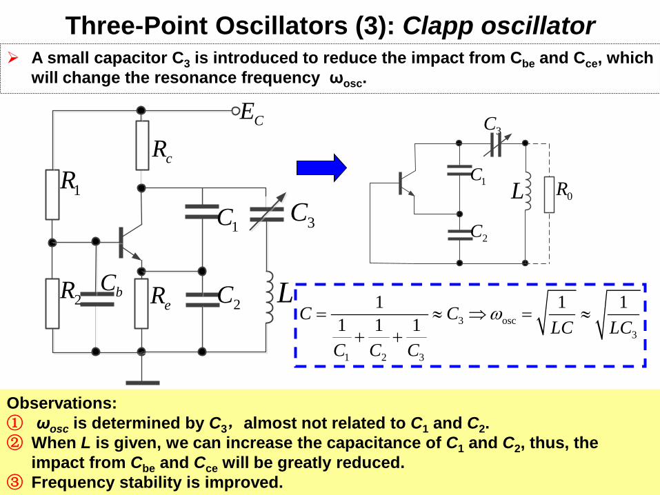
Three-Point Oscillators (3): Clapp oscillator
bC
1R
2ReR
CE
1C
2C L
3C
cR
3 osc3
1 2 3
1 1 11 1 1C C
LC LCC C C
ω= ≈ ⇒ = ≈+ +
Observations: ① ωosc is determined by C3,almost not related to C1 and C2.② When L is given, we can increase the capacitance of C1 and C2, thus, the
impact from Cbe and Cce will be greatly reduced. ③ Frequency stability is improved.
1C
2C
L
3C
0R
A small capacitor C3 is introduced to reduce the impact from Cbe and Cce, which will change the resonance frequency ωosc.

石英晶体振荡器
17

5.7石英晶体振荡器
• 一、晶体的物理特性
• 1.结构特点
• 2. (基波)等效电路• 特点:
等效电感Lq非常大(几~十分之几H);等效电容Cq非常小(百分之几pf);
等效电阻rq非常小(几~几百Ω);C0为静电容(几pF~几十pF, Cq《C0)
切面
石英晶体利用压电效应和反压电效应实现机械能量与电能的转换
C0 Cq
Lq
rq
(几万~几百万) 18

二、电特性• 1.谐振频率及近似电抗特性
1s
q qL Cω =串谐频率:
0
0
1p
q
C CL
C C
ω =
+
并谐频率:
19
工作区域:串联谐振或感性区域

三、晶体振荡器电路1.并联型晶体振荡器
• 晶体工作在ωp附近,晶体等效为电感。
电容三端(皮尔斯) 电感三端(密勒)
20

改进的Clapp振荡器
C1C2
C
C0Cq
Lq
C1
C2
C
1.振荡频率的确定
C0
Cq
LqC1
C2
C
21
0 1111
111
CCC
CCC q
+++
+=∑
21

讨论:调节C可使f0产生微小的变动。
* 若C很大,取C→∞,得:
*若C很小,取C→0,得:
𝐶𝐶 ≪ 𝐶𝐶1,𝐶𝐶 ≪ 𝐶𝐶2CCC
CCCC
q
q
+++
=∑0
0 )(
CCCCCC
Lf
q
qq ++
+=∴
0
00 )(
2
1
π
sqq
fCL
f ==∴π2
10
p
q
f
CCCC
Lf =
+
=∴
0
00
2
1
π
可见,无论如何调节C,f0总是在fp与fs之间。
一般,C取得较小,使f0工作在稍低于fp的数值。 22

2.串联型晶体振荡器
• 反馈信号经石英晶体JT后,才能送到发射极和基极之间。石英晶体的串联谐振阻抗接近于0,可以认为短路。此时正反馈最强,满足振荡条件。
23

3.晶体的正确使用
• 1)作为电路的电感或短路元件;
• 2)按规定配合负载电容;
• 3)激励电平不超过规定;
• 4)合理选择恒温槽温度。
24

25
Voltage-Controlled Oscillators: Characteristic
The output frequency varies from ω1 to ω2 (the required tuning range) as the control voltage, Vcont, goes from V1 to V2.
The slope of the characteristic, KVCO, is called the “gain” or “sensitivity” of the VCO and expressed in rad/Hz/V.

26
Varactors(可变电容)
Varactor is a voltage-dependent capacitor.
Two important attributes of varactor design become critical inoscillator design:
The capacitance range i.e. ratio of maximum to minimumcapacitance that varactor can provide.
The quality factor of the varactor.

27
PN Junction Varactor
Varactor capacitance of reversed-biased PN junction.
Cjo is the capacitance at zero bias,
V0 is the built-in potential, (≈0.7 to 0.8);
m is an exponent around 0.3 in integrated structure;
VD (<1V) is a reverse bias, and 1+VD/V0 varies between 1 to 2;
Thus, the capacitance range, Cj,max/Cj,min is roughly 1.23.

28
MOS Varactor ?
A regular MOSFET exhibits a voltage dependent gate capacitance.The non-monotonic behavior with respect to gate voltage limits the
design flexibility.
Variation of gate capacitance with VGS
Regular MOS device:

29
Accumulation Mode MOS VaractorAccumulation-mode MOS varactor is
obtained by placing an NMOS inside an n-well.
The variation of capacitance with VGSis monotonic.
The C/V characteristics scale well with scaling in technology, approach its saturated levels of Cmax and Cminfor VGS ≈±0.5V in 65-nm devices).
Unlike PN junction varactor, this structure can operate with positive and negative bias so as to provide maximum tuning range.
C/V characteristics of varactor

30
VCO Using MOS Varactors
Since it is difficult to vary the inductance electronically, we only vary the capacitance by means of a varactor.
MOS varactors are more commonly used than pn junctions, especially in low-voltage design.
First, the varactors are stressed for part of the period if Vcont is near ground and VX (or VY ) rises significantly above VDD.
Second, only about half of Cmax - Cmin is utilized in the tuning.

31
Example: VDD as the “Control Voltage”As explained in previous example, the cross-coupled oscillator exhibits sensitivity to VDD. Considering VDD as the “control voltage,” determine the gain.
The junction capacitance, CDB, is approximated as
If C1 includes all circuit capacitances except CDB
where ΦB denotes the junction’s potential and m is around 0.3 to 0.4.

32
VCO as a Frequency Modulator
Let us now consider an unmodulated sinusoid, V1(t) = V0 sin ω1t. Called the “total phase,”the argument of the sine, ω1t, varies linearly with time in this case, exhibiting a slope of ω1.
Define the instantaneous frequency as the time derivative of the phase:
Since a VCO exhibits an output frequency given by ω0 + KVCOVcont, we can express its output waveform as
A VCO is simply a frequency modulator. For example, the narrow-band FM approximation holds here as well.