CHAPTER 7 BEAMFORMING TECHNIQUES -...
39
150 CHAPTER 7 BEAMFORMING TECHNIQUES 7.1 INTRODUCTION Smart antenna technology can be used to increase coverage of the wireless system. Smart antennas have low power dissipation, improved link quality and increased spectral efficiency (Ahmed El Zooghby 2005). These enhancements are achieved by directing multiple radiation lobes towards desired transmitters or receivers and nulls towards interferers (Rappaport 1998). Implementing such a system in real-time is complex and expensive. A simpler, cheaper and sufficiently effective alternative is to use beamforming technique. Beamforming finds its applications in Mobile communication for pointing the beam towards a particular mobile terminal and receive the signal from the mobile. There are two types of beamforming namely analog and digital. In digital beamforming the signals are propagated through individual channels and are finally combined at the baseband level. In analog beamforming the signals from various directions are combined in the front end of the receiver and are given through a single channel for processing at the baseband level. The beamformer combines energy over antenna aperture, obtaining a certain antenna gain in a given direction while having attenuation in other directions. In both analog and digital domains the common methods used to create directional beams are either by time delay (time shift) or phase shift. The time delay approach allows forming and steering the beam by adding adjustable
-
Upload
phungthien -
Category
Documents
-
view
227 -
download
4
Transcript of CHAPTER 7 BEAMFORMING TECHNIQUES -...

150
CHAPTER 7
BEAMFORMING TECHNIQUES
7.1 INTRODUCTION
Smart antenna technology can be used to increase coverage of the
wireless system. Smart antennas have low power dissipation, improved link
quality and increased spectral efficiency (Ahmed El Zooghby 2005). These
enhancements are achieved by directing multiple radiation lobes towards
desired transmitters or receivers and nulls towards interferers (Rappaport
1998). Implementing such a system in real-time is complex and expensive. A
simpler, cheaper and sufficiently effective alternative is to use beamforming
technique. Beamforming finds its applications in Mobile communication for
pointing the beam towards a particular mobile terminal and receive the signal
from the mobile.
There are two types of beamforming namely analog and digital. In
digital beamforming the signals are propagated through individual channels
and are finally combined at the baseband level. In analog beamforming the
signals from various directions are combined in the front end of the receiver
and are given through a single channel for processing at the baseband level.
The beamformer combines energy over antenna aperture, obtaining a certain
antenna gain in a given direction while having attenuation in other directions.
In both analog and digital domains the common methods used to create
directional beams are either by time delay (time shift) or phase shift. The time
delay approach allows forming and steering the beam by adding adjustable

151
time delay steps. Time delay is independent from the operating frequency and
bandwidth. Since it is difficult to generate time delays in both the analog and
digital domains, they are used only strictly with large arrays or when the
bandwidth of the system is wide. In the case of phase shifting approach, a
phase is introduced instead of applying true time delays for each receiver and
it is simple to introduce such compensation as this works properly with
narrow band systems or small arrays.
Many receivers are connected to different antenna elements.
Having antenna elements as separate structures occupies more space.
Therefore antenna elements are combined to form array. In the antenna array
if the individual antenna elements are excited separately the array is Phased
Antenna Array. The Phased Array Antenna (PAA) is capable of steering the
beam electronically in a particular direction. The advantages of PAA are that
it gives very narrow beam width and minimum side lobe levels.
In this chapter, two methods of analog beamforming with Phased
Array Antenna (PAA) are proposed. One is an active beamforming system
and the other method is a passive beamforming system. The active
beamforming system uses PAA, LNA, variable attenuator and phase shifter.
The passive beamforming system uses PAA, Butler matrices, Single Pole
Eight Throw (SP8T) switches to form a directional beam. The steering of the
beam is accomplished by the Butler Matrices. This system has the advantages
of linearity, good dynamic range and is reciprocal in nature. The same
network can be used for transmitter and receiver RF stages.
7.2 LITERATURE SURVEY
Efficient beamforming algorithms are compared by Ronald Mucci
(1984). All the beamforming methods use individual antenna elements. Beam
selection performance analysis of multi-beam antenna system is discussed by

152
Matsumoto et al (1997). Jeon et al (2001) has proposed planar array smart
antenna system for hybrid analog-digital beamforming. Factors to be
considered in implementing smart antenna systems are proposed by Weon-
Ceol Lee et al (2005). Fakoukakis et al (2005) have proposed the
Development of an Adaptive and a Switched Beam Smart Antenna System
for Wireless Communications for 2.4GHz ISM band with separate antenna
systems. The design, working and performance of Microstrip antennas are
discussed by Bahl and Bhartia (1986), Hansen (1997) and James and Hall
(1989). Chao-Wei Wang et al (2007) have proposed a New Planar Artificial
Transmission Line and Its Applications to a Miniaturized Butler Matrix. A
Single-Layer Hollow-Waveguide 8-Way Butler Matrix has been discussed by
Shin-ichi Yamamoto et al (2005). Tayeb Denidni and Taro Eric Libar (2002)
have done Experimental Investigation of a microstrip Planar Feeding Network
for a Switched-Beam Antenna Array.
7.3 ACTIVE ANALOG BEAMFORMING WITH PAA
Active beamforming system for 2.4GHz is designed and
implemented. The active beamforming is implemented in three steps. First,
the design of PAA which produces a narrow beam and Right Hand Circular
Polarization (RHCP) is proposed and simulated. Second, the excitation
amplitudes for non-uniform amplitude distribution of antenna elements are
calculated. The excitation amplitudes are calculated to have low side lobes.
Third, the calculation of complex weights in terms of magnitudes and phase
to provide steering commands for beamforming in particular direction. The
beam can be steered in both azimuth and elevation planes with the help of
beamformer circuits designed at 2.4 GHz with a bandwidth of 20MHz. To
design PAA, first a single patch antenna element is designed and its
performance is studied. The specifications of the design are given in
Table 7.1.

153
Table 7.1 Specifications of PAA
Parameters Values
Frequency 2.4 GHz
Bandwidth 20 MHz
Axial ratio 3dB (maximum)
PolarizationRHCP
(Right Hand Circular Polarization)
Impedance 50 ohms
Axial ratio is the difference between the 'horizontal' and 'vertical'
(or otherwise orthogonal) components. In a pure circularly polarized wave
both electric field components have equal magnitude and the axial ratio is 1 or
0 dB. Axial Ratio of maximum 3 dB is acceptable (Bahl and Bhartia 1986).
7.3.1 Single Circularly Polarized Patch Design
The selection of substrate dielectric constant ‘ r’ and the substrate
thickness ‘h’ plays important role in the antenna design. Low dielectric
constant increases radiated power but at the cost of larger size. A thicker
substrate besides being mechanically strong will increase radiated power and
improves impedance bandwidth. Thicker substrates do have the disadvantages
of increasing weight and dielectric loss. Thicker substrates with low dielectric
constant increases radiated power, providing better efficiency and larger
bandwidth but at the expense of larger element size as given by Balanis
(1997). The dielectric chosen is RT Duroid 5870 with loss tangent, 0.0012;
height, 1.6 mm; and r, 2.32. Selection of these parameters is followed by
calculation of patch dimension. The value of the patch width W is calculated
with resonant frequency fr and the velocity of light, c as

154
r rW c/ 2f 2 / ( 1) (7.1)
The effect of fringing field increases the length (L) on both sides of
the patch. The increase in length by small factor due to fringing is called
effective length (Le). Effective length is calculated by including the effective
dielectric constant re, and is given as
e
r re
cL(2f )
(7.2)
The effective dielectric constant re, and extension in length L on
one side of the patch can be calculated as
1r r 2
re
( 1) ( 1) h[1 12 ]W2 2 (7.3)
re
re
W( 0.300 0.264)
hL 0.412hW
( 0.258 0.813)h
(7.4)
Length of the patch L is given by,
eL L 2 L (7.5)
The patch antenna works when excitation is given through a feed.
Coaxial line feed is used for the excitation of the patch antenna. It is better to
choose yf = W/2 if W L as proposed by Kara (1996). A simple method for
calculating xf that does not need radiation resistance is given by Bhal and
Bhartia (1986) and Kara (1996). The feed is not radiating and only the patch
is radiating.

155
The feed point F (xo, yo) is located at xo = xf and 0 yo = yf W,
where xf is the inset distance from the radiating edge given by (7.6).
f
re
Lx(2 (L))
(7.6)
where, re is the effective dielectric constant with fringing effects and is
given as
2/1rrre ]L/h121[2/)1(2/)1()L( (7.7)
Circular polarization can be achieved by dual feed or single feed
method. In this chapter, single point feed type is chosen because the antenna
should be compact and the bandwidth required is less than 1% of the
operating frequency (20 MHz). Hybrid coupler is not required in single feed
method. Single point feed can be of two types – Type A and Type B
depending on the feed location. It is type A feed when the feed location is on
the x or y axis and the feed is Type B if the feed is placed on the diagonal axis
of a patch as shown in Figure 7.1.
X
Y
F
X
Y
F
Type A Feed Type B Feed
Figure 7.1 Type A and Type B Feed

156
Type A feed is chosen for the design and the design equation given
by Ramesh Garg et al (2000) is chosen to design the feed. For the type-A feed
the design equation is given as
2/1Q/Ss o (7.8)
where, s , area of feed; S, area of the square patch and Qo, unloaded Q
factor. Using the above design equation along with dimensions and dielectric
thickness of single patch, the feed size is calculated. The patch antenna
dimensions with feed location after optimization is shown in Figure 7.2.
Figure 7.2 Dimensions of the patch in mm
Number 1 in the Figure 7.2 near the feed location denotes port
number. The plot of VSWR and return loss are shown in Figure 7.3a and 7.3b
respectively.
F (8.5, 0.7) mm
4.2 mm
40 mm
40 mm(0, 0)

157
(a) VSWR
(b) Return Loss
Figure 7.3 Parameters of Single Patch antenna
The VSWR and the return loss are low at the designed frequency.
The resonant frequency (fr) of the designed antenna is obtained as 2.412565
GHz. Simulation results at resonant frequency of the designed single patch are

158
as follows: VSWR, 1.005; return loss, -51.705dB; axial ratio, 0.145dB;
impedance at feed point, 49.8 + j 0.211 ; Gain, 6.6 dBi; Bandwidth, 20MHz;
resonant frequency, 2412.565 MHz; polarization, RHCP; antenna efficiency,
84.5865%. The radiation pattern at elevation plane and the 3D beam pattern
are shown in Figure 7.4a and 7.4b respectively.
a) Elevation Pattern (b) Main Lobe
Figure 7.4 Plots of antenna parameters.
The radiation properties of the patch antenna observed from the
radiation in elevation plane are given in Table 7.2.
Table 7.2 Radiation properties of patch antenna
Parameters Total fieldRHC
polarization
LHC
polarization
Gain (dBi) 6.64514 6.64483 -6.70265
Directivity(dBi) 7.37213 7.37183 -5.97566
3-dB beam width
, ) (degrees)87.2239, 88.5629 87.0395, 88.2769 18.6259, 147.825
From the Table 7.2 it is inferred that the patch antenna provides
RHC polarization. The gain and directivity are high for RHCP than LHCP. It
is clear from Figure 7.5 and Figure 7.6 that the input impedance obtained is

159
close to 50ohms and the gain is 6.6dBi at resonant frequency of 2.4125GHz
for a single patch antenna.
Figure 7.5 Impedance plot of single patch antenna
Figure 7.6 Gain of single patch antenna
7.3.2 Planar Array Design
The required specification of the array is to produce a beam width
of 15° in both elevation and azimuth planes; scannable to 45° in both planes

160
0.53
0.53
and side lobe should be lees than 25 dB than main lobe. The design procedure
is adopted from Robert Elliot (2000). A planar array of size 8 x 8 with
element spacing of 0.53 in both axes is designed to meet the specifications.
The structure of the designed planar array is shown in Figure 7.7.
Figure 7.7 Planar Array Geometry
The single patch is used as the array element for this planar array.
The simulation results of the designed 8 x 8 planar patch antenna array at
resonant frequency (fr) are as follows: VSWR, 1.0615; Return Loss, -30.49
dB; Axial ratio, 1.1dB; impedance at feed point, 49.3 - j 0.16 ; gain,
19.7dbi; bandwidth, 20MHz; resonant frequency, 2412.565 MHz;
Polarization, RHCP; 3 dB beam width: elevation plane, 15º, azimuth plane,
15º; side lobe level, -25dB.The plot of VSWR and return loss are shown in
Figure 7.8a and 7.8b respectively.

161
(a) VSWR
(b) Return Loss
Figure 7.8 Plots of antenna array parameters
The elevation plane radiation pattern and the main lobe are shown
in Figure 7.9a and 7.9b respectively.

162
(a) Elevation Pattern
(b) Main Lobe
Figure 7.9 Parameters of Array Antenna

163
E theta at 0°
E Theta at 90°
Axial Ratio (AR) is calculated by taking the difference of gain
between the E theta component at phi=0° and phi=90° for broad side case
from Figure 7.10.
(E theta component at phi=0°) - (E theta component at phi=90°) = 17.607 -
15.557 = 2.1 dB.
Figure 7.10 E theta components – Cartesian Plot
7.3.3 Array Beamsteering
In order to steer the beam electronically, necessary phase shifts
along with excitation amplitudes has to be applied. For M x N array, the phase
steering command at each element is given as,
mn m x n y (7.9)

164
where o ox kdxsin cos , sin sino o
y kdy , 2k , o and o are
scan angles in elevation and azimuth planes, n = 1, 2,…..M and m = 1,
2,….N,
The phase shift to be applied for the element at (m,n) position of
array is, x o o y o o
2mn md sin cos nd sin sin , where dx, dy are the element
spacing in x and y axis respectively.
The excitation amplitude applied to each element is
mnj
mn mnV V e where, Vmn is the excitation coefficient calculated from
non-uniform amplitude distribution.
In order to obtain a narrow main beam with lowered side lobe, non-
uniform amplitude distribution has to be used. Two methods of non-uniform
amplitude distribution, namely Taylor and Dolph-Chebyshev distributions are
used. The Taylor distribution array pattern has a wider main lobe than the
corresponding Dolph–Chebyschev distribution, but has low side lobes at the
expense of approximately 2° increase in half power beam width. Thus the
array with the smoothest amplitude distribution will have the smallest side
lobes and larger half power beam widths. Scan angle denotes the direction in
terms of ( , ) in which the beam has to be steered. A comparison of half
power beam widths and side lobe of the array at different scan angles for both
distributions is given in Table 7.3

165
Table 7.3 Beam width and side lobe of Taylor and Dolph – Chebyshev
distribution.
Taylor DistributionDolph – Chebyshev
DistributionScan Angle
(degrees) 3dB Beam
width (degrees)
Side Lobe
at (dB)
3 dB Beam width
(degrees)
Side Lobe
at (dB)
(0,0) (17.2,17.4) -15 (15.4,15.6) -5
(30,0) (21.6,19.3) -12 (19.6,17.4) -3
(45,0) (24.8,19.4) 0 (22.9,17.4) 4
(-45,30) (23.5,17.4) -30 (21.1,15.4) -25
(45,45) (23.3,18.8) -30 (20.9,17.1) -25
(-45, -45) (23.3,17.1) 0 (21.2,15.5) 4
The gain and directivity of the antenna array for different scan
angles for Taylor and Dolph-Chebychev distribution are given in Table 7.4.
Table 7.4 Gain and Directivity for different scan angles
Taylor DistributionDolph-Chebyshev
DistributionScan
Angle
(degrees) Gain (dBi)Directivity
(dBi)
Gain
(dBi)
Directivity
(dBi)
( 0, 0 ) 20.8 21.3 21.9 22.4
( 30, 0) 20.3 20.5 21.3 21.5
( 45, 0) 18.5 19 19.5 19.8
( -45, 30) 19.2 19.6 20.3 20.7
( 45, 45) 18.7 19.2 19.7 20.1
(-45,-45) 18.8 19.6 19.9 20.5

166
The radiation patterns of the array are shown for maximum and
minimum scan angles. The radiation pattern of the array, in elevation and
azimuth plane, for a scan angle of (-45°, -45°) is shown in Figure 7.11, with
dotted line showing Dolph-Chebyschev distribution and thicker line showing
Taylor distribution pattern. Similarly, the radiation pattern of the array for a
scan angle of (45°, 45°) is shown in Figure 7.12.
(a) Elevation Pattern
(b) Azimuth Pattern
Figure 7.11 Elevation and Azimuth Pattern of array at a scan angle of
(-45°, -45°)

167
(a) Elevation Pattern
(b) Azimuth Pattern
Figure 7.12 Elevation and Azimuth Pattern of array at a scan angle of
(45°, 45°)
-30
60
30

168
7.3.4 RF Beamformer
The Phased Array Antenna is composed of a group of similar
antennas, each with its variable attenuator, phase shifter and a summing
network, which gives a resulting signal representing a beam on an expected
location. Figure 7.13 shows the block diagram of the RF beamformer.
LNAVariable
Attenuator
Phase
Shifter
LNAVariable
Attenuator
Phase
Shifter
LNAVariable
Attenuator
Phase
Shifter
1
8
2
Figure 7.13 RF beamformer to combine the output of 8 columns of a row
8 RF beamformers are used to combine all 8 columns of each row
separately. The excitation coefficients are calculated in terms of magnitude
(dB) and phase (degrees) for different scan angles using Dolph-Chebychev
distribution and Taylor distribution. Magnitude of the excitation coefficients
using Taylor distribution for scan angles (45°, 0°), (45°, 45°) and (-45°, -45°)
is same and is given in Table 7.5. Magnitude of the excitation coefficients
using Dolph-Chebychev distribution for scan angles (45°, 0°), (45°, 45°) and
(-45°, -45°) is same and is given in Table 7.6.

169
Table 7.5 Magnitude in dB using Taylor distribution for Scan angle
(45°, 0°), (45°, 45°) and scan angle (-45°, -45°)
Row Column
1
Column
2
Column
3
Column
4
Column
5
Column
6
Column
7
Column
8
1 -67.042 -48.785 -38.814 -33.521 -33.521 -38.814 -48.785 -67.042
2 -48.785 -30.528 -20.557 -15.264 -15.264 -20.557 -30.528 -48.785
3 -38.814 -20.557 -10.587 -5.2936 -5.2936 -10.587 -20.557 -38.814
4 -33.521 -15.264 -5.2936 0 0 -5.2936 -15.264 -33.521
5 -33.521 -15.264 -5.2936 0 0 -5.2936 -15.264 -33.521
6 -38.814 -20.557 -10.587 -5.2936 -5.2936 -10.587 -20.557 -38.814
7 -48.785 -30.528 -20.557 -15.264 -15.264 -20.557 -30.528 -48.785
8 -67.042 -48.785 -38.814 -33.521 -33.521 -38.814 -48.785 -67.042
Table 7.6 Magnitude in dB using Dolph-Chebychev distribution for
Scan angle (45°, 0°), (45°, 45°) and (-45°, -45°).
Row Column
1
Column
2
Column
3
Column
4
Column
5
Column
6
Column
7
Column
8
1 1 1.5464 2.2296 2.6467 2.6467 2.2296 1.5464 1
2 1.5464 2.3913 3.4478 4.0927 4.0927 3.4478 2.3913 1.5464
3 2.2296 3.4478 4.9711 5.901 5.901 4.9711 3.4478 2.2296
4 2.6467 4.0927 5.901 7.0048 7.0048 5.901 4.0927 2.6467
5 2.6467 4.0927 5.901 7.0048 7.0048 5.901 4.0927 2.6467
6 2.2296 3.4478 4.9711 5.901 5.901 4.9711 3.4478 2.2296
7 1.5464 2.3913 3.4478 4.0927 4.0927 3.4478 2.3913 1.5464
8 1 1.5464 2.2296 2.6467 2.6467 2.2296 1.5464 1

170
The phase of excitation coefficients for each antenna element due
to Taylor distribution and Dolph-Chebychev distribution is same for same
scan angle. Phase values for both distributions at scan angle (45°, 0°) is given
in Table 7.7.
Table 7.7 Phase values of elements of array in degrees for scan angle (45°, 0°)
Row Column
1
Column
2
Column
3
Column
4
Column
5
Column
6
Column
7
Column
8
1 -90 -180 90 0 -90 -180 90 0
2 -90 -180 90 0 -90 -180 90 0
3 -90 -180 90 0 -90 -180 90 0
4 -90 -180 90 0 -90 -180 90 0
5 -90 -180 90 0 -90 -180 90 0
6 -90 -180 90 0 -90 -180 90 0
7 -90 -180 90 0 -90 -180 90 0
8 -90 -180 90 0 -90 -180 90 0
The phase of excitation coefficients for each antenna element is
same for both distributions for scan angle (45°, 45°) is given in Table 7.8.
Table 7.8 Phase values of elements of array in degrees for scan angle
(45°, 45°)
Row Column
1
Column
2
Column
3
Column
4
Column
5
Column
6
Column
7
Column
8
1 -180 90 0 -90 -180 90 0 -90
2 90 0 -90 -180 90 0 -90 180
3 0 -90 -180 90 0 -90 -180 90
4 -90 -180 90 0 -90 -180 90 0
5 -180 90 0 -90 -180 90 0 -90
6 90 0 -90 -180 90 0 -90 -180
7 0 -90 -180 90 0 -90 -180 90
8 -90 -180 90 0 -90 -180 90 0

171
The phase of excitation coefficients for each antenna element is
same for both distributions for scan angle (-45°, -45°) is given in Table 7.9.
Table 7.9 Phase values of elements of array in degrees for scan angle
(-45°, -45°)
Row Column
1
Column
2
Column
3
Column
4
Column
5
Column
6
Column
7
Column
8
1 0 90 -180 -90 0 90 -180 -90
2 -90 0 90 -180 -90 0 90 -180
3 -180 -90 0 90 -180 -90 0 90
4 90 -180 -90 0 90 -180 -90 0
5 0 90 -180 -90 0 90 -180 -90
6 -90 0 90 -180 -90 0 90 -180
7 -180 -90 0 90 -180 -90 0 90
8 90 -180 -90 0 90 -180 -90 0
The signal from the each antenna element is applied to attenuator
through the LNA. The signal from each element is processed in the attenuator
and phase shifter based on the excitation coefficients of the Taylor
distribution or Dolph-Chebychev distribution. The signal after the attenuator
is combined column wise. The power received is calculated column wise and
the total power received is calculated by combining the power from individual
columns. The procedure is repeated for different scan angles for both Taylor
distribution and Dolph-Chebychev distributions. The output power at each
column and total power from the array for Dolph-chebychev and Taylor
distributions are given in Table 7.10 for different scan angles.

172
Table 7.10 Output power from the array for Taylor and Dolph-
Chebychev distribution
Taylor Distribution (dB, Degrees)Dolph-Chebychev
Distribution (dB, Degrees)Scan
angle(45°, 0°) (45°, 45°) (-45°, -45°) (45°, 0°) (45°, 45°) (-45°, -45°)
Column 1 0.261, 90 0.155, 79 0.128, -10 12, -90 0.06, -162 0.06, 18
Column 2 2.274, 180 0.08, -178 0.086, 92 11, 179 0.09, 85 0.13, 48
Column 3 5.582, 90 0.485, 31 0.484, -122 8.64, 92 0.17, 37 0.17, -150
Column 4 8.647, 0 0.915, 49 0.906, -41 8.6, 1.8 0.08, -117 0.07, -63
Column 5 7.0468, 90 0.80, -127 0.799, 37 8.7, -92 0.12, 179 0.117, 10
Column 6 9.403, 180 0.421, 143 0.430, 127 8.7, 178 0.23, 126 0.21, 109
Column 7 2.161, 90 0.157, -2 0.139, -91 10.8, 91 0.07, -60 0.07, 120
Column 8 0.261, 0) 0.129, -73 0.133, -19 12, -.01 0.24, 126 0.05, 5.4
Total
power0.687,-34 0.258,-73 0.240, -16 0.1, -133 0.07, 131 0.06, 71
The signals from the different elements of the PAA are combined.
The power received after combining all the signals is found for the Taylor and
Dolph-Chebychev distributions for different scan angles. The signals received
from different directions are combined into a single unidirectional beam in a
particular direction.
7.4 PASSIVE ANALOG BEAMFORMING WITH PAA
Passive beamforming is a switched RF beamforming. Passive
beamforming is implemented using PAA, Butler matrix and Single Pole Eight
Throw (SP8T) switch. The PAA is designed and implemented as a 64 element
patch antenna array.

173
7.4.1 Phased Array Antenna Design and Implementation
A single square patch antenna is designed for 900MHz and the
dimensions of the patch are calculated. In the design procedure of single
patch, first the unloaded Quality factor (Qo) of the patch is determined. For
better accuracy Qo should be selected to ensure the patch radiation efficiency
greater than 90%. The single patch antenna is designed for frequency of 900
MHz producing Right Hand Circular Polarization (RHCP). For this design
with h = 1.6 mm, o =124 mm, h / o = 0.12 and efficiency of 90%, the Qo is
found to be 50. The calculated length is 108.8 mm. Hence the dimension of
square patch is 108.8 x 108.8 mm. The feed point coordinate is (35.9, 64.6)
mm, i.e. 35.9 mm from the edge towards the center of the patch in the x-axis
and at the middle along the y-axis. In this work, the dielectric chosen is RT
Duroid 5870 with loss tangent of 0.0012, height of 1.6 mm (1/16”) and the
dielectric constant of the substrate r 2.32 . The impedance is 50 at the
design frequency. The designed patch is shown in Figure 7.14.
Figure7.14 Single Patch with Dimensions and Feed point

174
The PAA is designed with this single patch antenna as the basic
element and the 8x8 array is formed by arranging the 64 single patch
antennas. The specifications for the PAA are same as for single patch. For
the given side lobe level of –25 dB the beam broadening factor is found to
be 1.06 and this factor is multiplied with the array length to get the actual
array length. Since the beam width required is 15° in both azimuth and
elevation plane and the scanning requirement for both planes are same, the
array length in terms of wavelength is same in both x and y-axis and is
found to be 4.24. To avoid multiple beams (grating lobes) during
scanning, the spacing between elements must be less than 0.59 . With this
condition the number of elements in both x and y-axis is found to be 7.2
which are rounded off to 8. Since the number of elements is rounded off to
eight the spacing between the elements becomes 0.53 . The PAA
structure without feed is shown in Figure 7.15 and its radiation pattern is
shown in Figure 7.16.
Figure 7.15 PAA with 64 elements

175
Figure 7.16 Radiation Pattern of PAA with 64 elements
The PAA is to be fed so that it can be connected to the Butler
matrix. There are two types of feed, series and parallel. The series feed and
the parallel feed are different in many aspects, the parallel feed provides a
larger bandwidth, while the series feed provides narrow bandwidths. The
main disadvantage of the parallel feed is that it suffers from more ohmic
losses since the structures used for feeding in parallel occupy more space. The
feed selected for PAA is combination of both series and parallel type of
feeding to achieve an acceptable tradeoff between bandwidth, radiation losses,
Ohmic losses and space.
The proposed antenna consists of 8 columns each one composed of
8 elements. The series feed of each column allows beam scanning in elevation
plane in the specified bandwidth. The design of the parallel feed provides the
power distribution necessary to maintain the side lobe level in azimuth below
the specifications for the entire bandwidth. The corporate feed provides a
power distribution that allows beam steering avoiding grating lobes. The
layout of corporate feed for the 64 element PAA is shown in Figure 7.17.

176
Figure 7.17 Layout of Corporate Feed for 64 Patches
The designed feed is connected to the PAA with 64 elements as
shown in Figure 7.18.
Figure 7.18 PAA with corporate feed

177
7.4.2 Butler Matrix
Butler Matrix is used to provide the necessary phase shift for a
linear antenna array. An N×N butler matrix can produce beams looking in
different directions with an N-element array (Neron and Jean-Sebastien
2003). A N×N butler matrix requires an (N/2) log2(N) 90° hybrids
interconnected by rows of (N/2)(log2(N)-1) fixed phase shifters to form the
beam pattern.
When a signal impinges upon the input port of the Butler Matrix, it
produces a different inter-element phase shifts between the output ports. The
Butler matrix consists of twelve 90° hybrids and eight cross couplers with two
ports and four cross couplers with four ports. When one of the input ports is
excited by an RF signal, all the output ports feeding the array elements are
equally excited but with a progressive phase between them. This results in the
radiation of the beam at a certain angle. The transmission line length and
width for various angles for impedance of 50 ohms is calculated using line
calculator in ADS tool. Line calculator is used to find the length and width of
the transmission line. The dimensions of the transmission line for various
impedances are given in Table 7.11.
Table 7.11 Dimensions of transmission line for various impedances
AnglesResistance Dimensions
22.5 45 67.5 90
Width(µm) 760.40 760.40 760.40 760.4050
Length(µm) 15247.60 30495.20 45742.00 60990.40
Width(µm) 1270.18 1270.18 1270.18 1270.1835
Length(µm) 14995.80 29991.60 44987.50 59983.30
Width(µm) 204.61 204.61 204.61 204.61100
Length(µm) 15839.90 31679.90 47519.80 63359.80
Width(µm) 425.56 425.56 425.56 425.5670.7
Length(µm) 15527.20 31054.30 46581.50 62108.70

178
7.4.2.1 Quadrature hybrid
The Hybrid coupler is often made of microstrip or stripline. These
couplers are 3 dB directional couplers with a 90° phase difference between
the outputs of the through and coupled lines. It is also known as a branch-line
hybrid. The schematic of hybrid coupler is shown in Figure 7.19.
Figure 7.19 Schematic of 3 dB directional couplers
The Layout of the coupler is shown in Figure 7.20. The length and
width of the coupler for various impedance values are shown in Table 7.12.
Figure 7.20 Layout of 3 dB directional couplers

179
Table 7.12 Dimensions of 3 dB directional couplers
Impedance 0Z =50 2/0Z =35
Length 60990.40 µm 59983.30 µm
Width 760.40 µm 1270.18 µm
The Table 7.13 gives the values of the substrate parameters used in
designing Quadrature hybrid and cross-coupler.
Table 7.13 Substrate parameters for microstrip structure
Substrate
parameter
Values
Er 2.2
Mur 1.0
H 254µm
Hu 3.9e+34 mil
T 17.50µm
Cond 4.1 e+7
TanD 0.0009
Rough 0.000mil
7.4.2.2 Cross-coupler
Cross-coupler also known as 0 dB couplers are an efficient means
of crossing two transmission lines with a minimal coupling between them. It
is observed that the planar implementation is made as a cascade of two hybrid
couplers (with slight modifications on line widths). Figure 7.21 is the
schematic design of Cross-coupler and Figure 7.22 is the layout design Cross-
coupler. The cross-coupler with two ports is used in the design of Butler
matrix.

180
Figure 7.21 Schematic of Microstrip Cross-coupler
a) Layout Design of Cross-coupler four Ports
b) Layout Design of Cross-coupler with two ports
Figure 7.22 Layout of cross couplers

181
7.4.2.3 Vertical Interconnection
The vertical interconnection shown in Figure 7.23 is used to
transmit a signal from one layer to the other by an electromagnetic coupling
only. There is no DC path between the 2 layers since they are AC coupled
only; a signal arriving on the upper transmission line (from the left)
eventually reaches the end of this transmission line. The discontinuity created
here radiates energy that is mostly coupled to the bottom line by the opening
in the ground plane (some power may radiate).
The following aspects must be considered to achieve an optimal
coupling between layers as well as a good matching of the transition:
1. A proper positioning of the line ends relative to the slot center
2. A proper dimensioning of the serial stub added at the end of
the transmission lines is necessary
3. The design of the slot in the ground plane: many shapes are
possible (circular, bowtie, rectangular, and so on), and the
dimensions should be carefully optimized
4. Orientation of the lines over the slot.
Figure 7.23 Layout of vertical interconnection
182
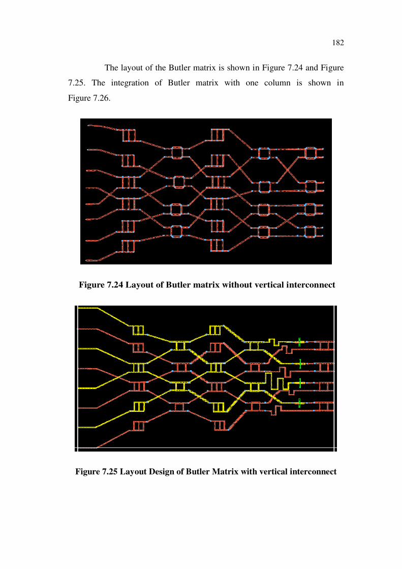
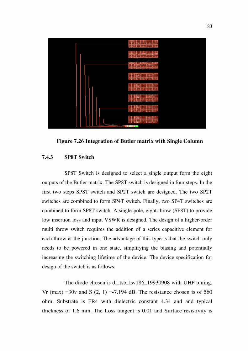
The layout of the Butler matrix is shown in Figure 7.24 and Figure
7.25. The integration of Butler matrix with one column is shown in
Figure 7.26.
Figure 7.24 Layout of Butler matrix without vertical interconnect
Figure 7.25 Layout Design of Butler Matrix with vertical interconnect
183
Figure 7.26 Integration of Butler matrix with Single Column
7.4.3 SP8T Switch
SP8T Switch is designed to select a single output form the eight
outputs of the Butler matrix. The SP8T switch is designed in four steps. In the
first two steps SPST switch and SP2T switch are designed. The two SP2T
switches are combined to form SP4T switch. Finally, two SP4T switches are
combined to form SP8T switch. A single-pole, eight-throw (SP8T) to provide
low insertion loss and input VSWR is designed. The design of a higher-order
multi throw switch requires the addition of a series capacitive element for
each throw at the junction. The advantage of this type is that the switch only
needs to be powered in one state, simplifying the biasing and potentially
increasing the switching lifetime of the device. The device specification for
design of the switch is as follows:
The diode chosen is di_tsb_lsv186_19930908 with UHF tuning,
Vr (max) =30v and S (2, 1) =-7.194 dB. The resistance chosen is of 560
ohm. Substrate is FR4 with dielectric constant 4.34 and and typical
thickness of 1.6 mm. The Loss tangent is 0.01 and Surface resistivity is

184
200K . The SP8T layout is shown in the Figure7.27. The insertion loss in
the SP8T switch is found to be -15dB.
Figure 7.27 Layout of SP8T Switch
7.4.4 Switched RF Beamforming System
The RF beamforming system has the advantage of easy
integration with existing architectures in base stations and offer reduced
complexity compared to IF Beamforming Systems. The front-end of
passive RF Switched beamforming system is shown in Figure 7.28.

185
Butler Matrix
8 x 8
S
P
8
T
S
P
8
T
S
P
8
T
1
8
Butler Matrix
8 x 8
Butler Matrix
8 x 8
Output
Figure 7.28 RF Switched Beamforming System
There are 64 antenna elements in the system that is realized in
the form of PAA with 8 elements in each row and 8 elements in each
column. The output of elements in 8 rows are combined column wise
using the 8×8 Butler matrix and SP8T switch and totally 8 outputs are
taken. This output of eight individual columns are further given to 8×8
Butler matrix and SP8T switch and combined as single output. The system
is implemented as shown in Figure 7.29.

186
Figure 7.29 Complete Layout of Switched RF Beamforming System

187
The results obtained for single cell, PAA without feed for 64
elements, PAA with feed for 64 elements and the complete system are given
in Table7.14.
Table7.14 Results of Passive Beamforming system
Parameters Single Patch
antenna
PAA without
feed for 64
elements
PAA with feed
for 64
elements
Switched RF
Beamforming
System
Power
radiated
(Watts)
4. 37096 e-5 1. 51257 e-5 5. 1301 e-6 0. 0166609
Directivity
(dB)
6. 94928 18. 5318 21. 61831 14. 8938
Gain
(dB)
5. 30524 11. 8807 10. 808 14. 3432
Radiation
Intensity
1.72 e -5 8. 58 e -5 5. 925 e-5 0. 04091
E max
(magnitude,
phase)
0.11, 83.89° 0.20, -3.03° 0.19, -1.4° 5.55, 125.45°
E max
(magnitude,
phase)
9.86x10⁻⁵
, -172.5° 0.14, 176.94° 0.08, 178.65° 0.00018, 51.34°
The results show that both the directivity and gain are improved in
the switched RF Beamforming system when compared with Single patch
antenna. PAA with feed and without feed gives more directivity but the gain
is decreased. The power radiated by the switched RF Beamforming system is
also larger. The maximum radiation is obtained for the maximum values of
Electric field intensity in the and directions. The maximum radiation after
combining the signals from different directions is obtained at an angle of

188
(125.45°, 51.34°) with maximum amplitude of Electric field intensity
5.55V/m in the direction.
7.5 CONCLUSION
Active beamforming circuit with PAA is implemented for 2.4GHz.
Design of Phased array antenna gives axial ratio (AR) of 2.1 dB maximum at
the desired scan angle of 45 . Two types of non-uniform amplitude
distributions namely, Dolph-Chebyshev distribution and Taylor distribution
are used for beamforming. Dolph-Chebyshev distribution gives narrow beam
width than Taylor distribution but the side lobes are constant. Taylor
distribution gives tapering side lobes with 2º broader beam width. This has
been observed at various scan angles. Also from the simulation results, it is
found that the beam broadening is more for scan angles greater than 45º.
Axial ratio (AR) also degrades when scanning away from the broadside.
The front end of Switched RF beamforming system is
implemented for 900MHz. Design and simulation of Sixty four cell patch
antenna has been implemented. Optimization of 64 cell array has been
done to obtain good response at the desired frequency by increasing the
number of sample points during simulation. Corporate feed design for the
phased array antenna is implemented and the antenna properties are
improved. An 8×8 Butler Matrix has been designed to change the
direction of radiated or received energy in a particular angle by the
transmitter or receiver. Butler matrix is interfaced with antenna array and
the radiation pattern is obtained with a phase shift of zero degree. Design
and implementation of Single pole eight throw switch is done and the
insertion loss is found to be -15 dB. The system works in the frequency
range of 900MHz and the results show that switched RF Beamforming
system provides good gain and directivity at 900MHz.