Chapter 7 · PDF fileChapter 7 Interfacing Circuits between the ... = average of two time...
36
Chapter 7 Interfacing Circuits between the Logic Gates Of Same Family, Different Families and Types
-
Upload
nguyenngoc -
Category
Documents
-
view
222 -
download
5
Transcript of Chapter 7 · PDF fileChapter 7 Interfacing Circuits between the ... = average of two time...
Chapter 7
Interfacing Circuits between the Logic Gates Of Same Family, Different Families and Types
Lesson 1
CHARACTERISTIC PARAMETERS
Ch07L1-"Digital Principles and Design", Raj Kamal, Pearson Education, 2006 3
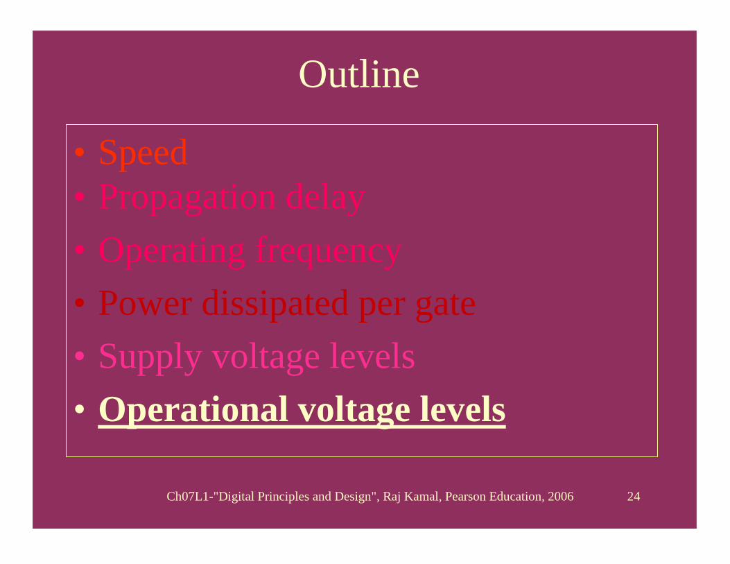
Outline
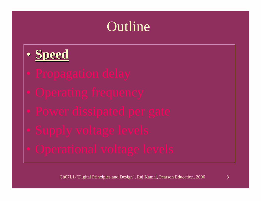
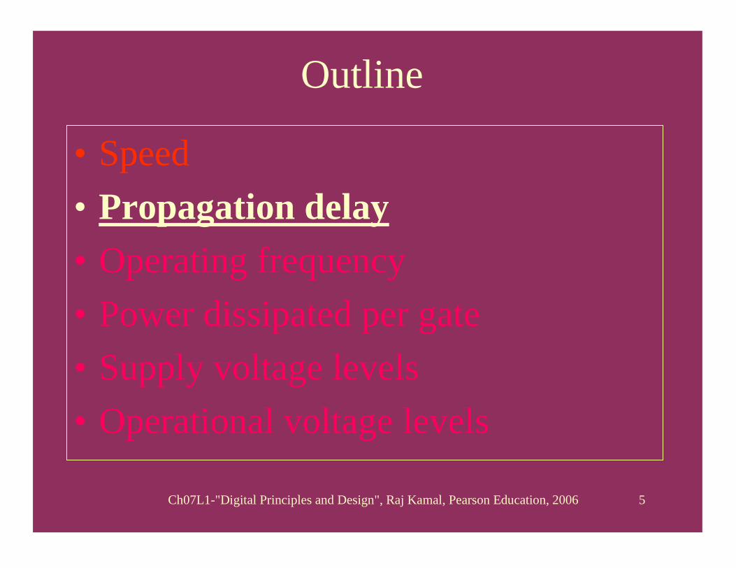
•• SpeedSpeed• Propagation delay • Operating frequency• Power dissipated per gate• Supply voltage levels• Operational voltage levels
Ch07L1-"Digital Principles and Design", Raj Kamal, Pearson Education, 2006 4
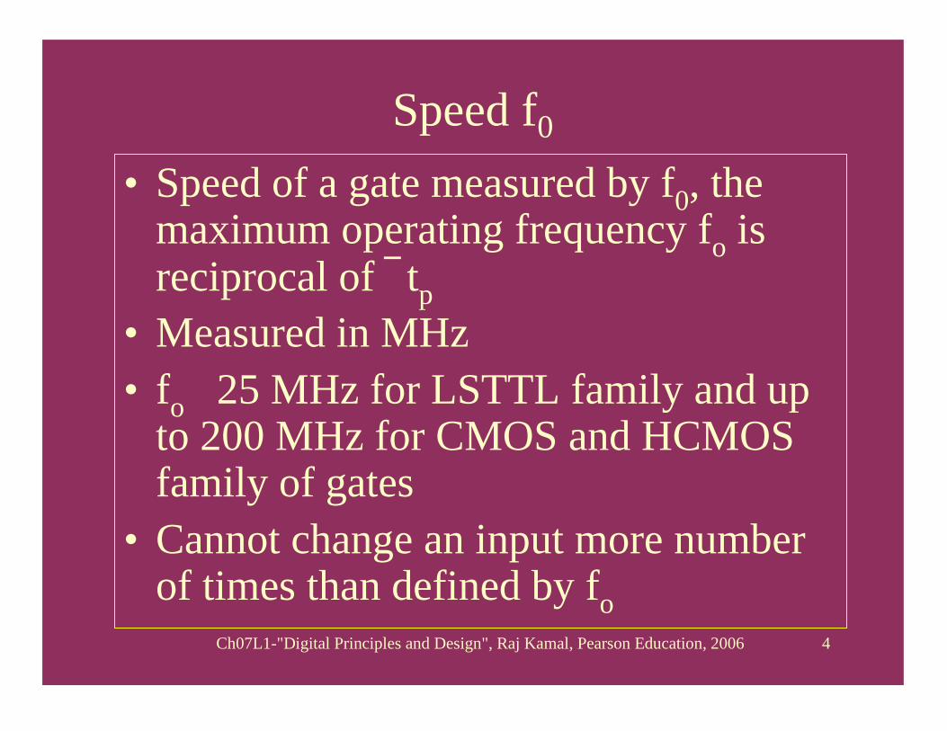
Speed f0
• Speed of a gate measured by f0, the maximum operating frequency fo is reciprocal of tp
• Measured in MHz• fo 25 MHz for LSTTL family and up
to 200 MHz for CMOS and HCMOS family of gates
• Cannot change an input more number of times than defined by fo
Ch07L1-"Digital Principles and Design", Raj Kamal, Pearson Education, 2006 5
Outline
• Speed• Propagation delay• Operating frequency• Power dissipated per gate• Supply voltage levels• Operational voltage levels
Ch07L1-"Digital Principles and Design", Raj Kamal, Pearson Education, 2006 6
Propagation delay
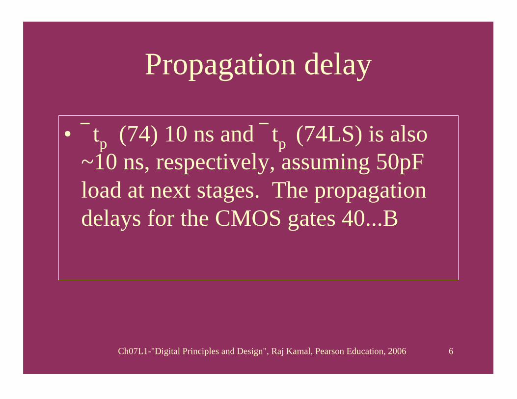
• tp (74) 10 ns and tp (74LS) is also ~10 ns, respectively, assuming 50pF load at next stages. The propagation delays for the CMOS gates 40...B
Ch07L1-"Digital Principles and Design", Raj Kamal, Pearson Education, 2006 7
Propagation Delay
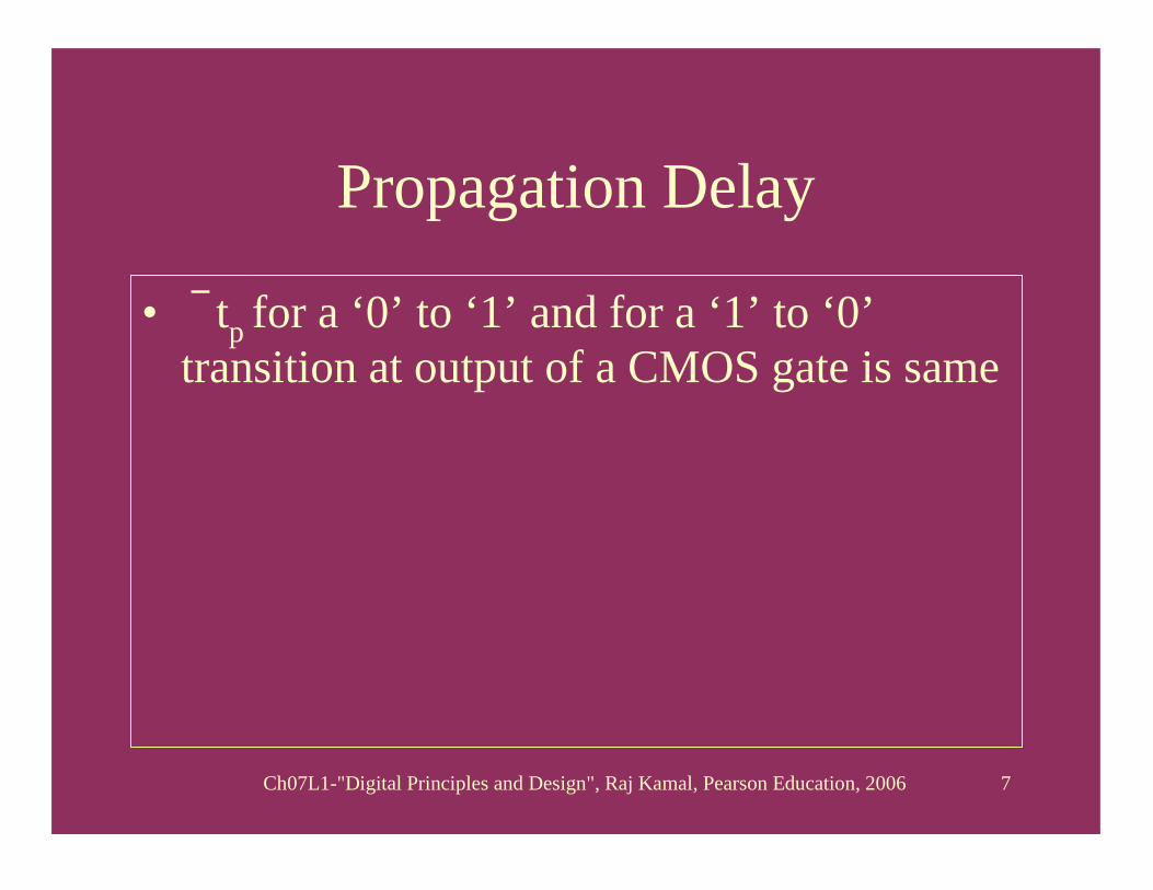
• tp for a ‘0’ to ‘1’ and for a ‘1’ to ‘0’transition at output of a CMOS gate is same
Ch07L1-"Digital Principles and Design", Raj Kamal, Pearson Education, 2006 8
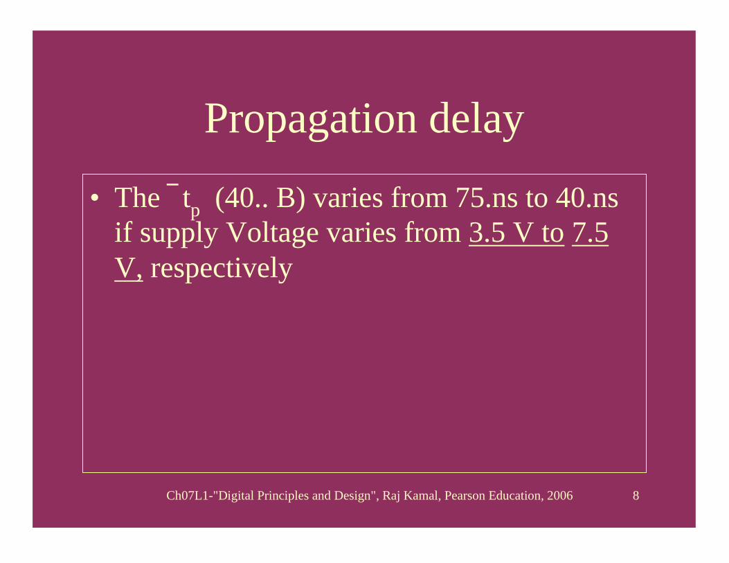
Propagation delay
• The tp (40.. B) varies from 75.ns to 40.ns if supply Voltage varies from 3.5 V to 7.5 V, respectively
Ch07L1-"Digital Principles and Design", Raj Kamal, Pearson Education, 2006 9
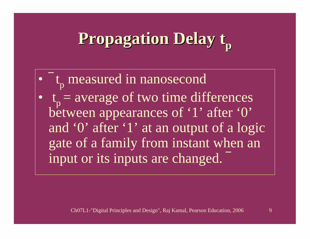
Propagation Delay tPropagation Delay tpp
• tp measured in nanosecond• tp = average of two time differences
between appearances of ‘1’ after ‘0’and ‘0’ after ‘1’ at an output of a logic gate of a family from instant when an input or its inputs are changed.
Ch07L1-"Digital Principles and Design", Raj Kamal, Pearson Education, 2006 10
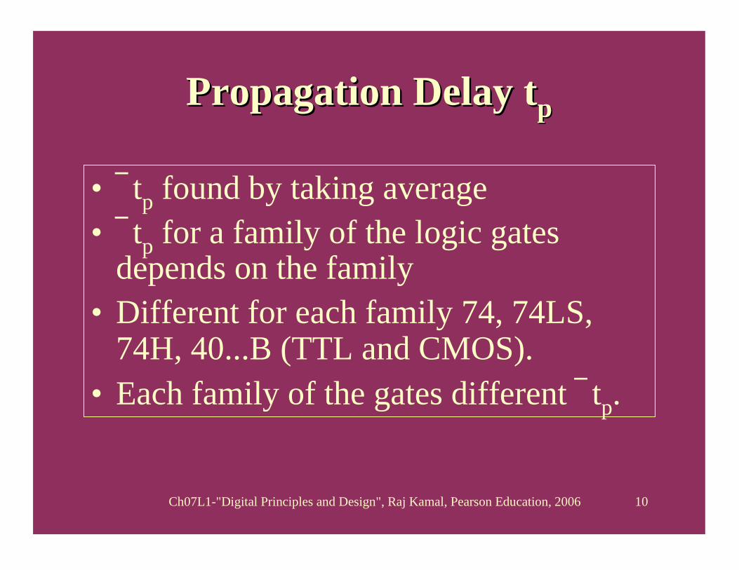
Propagation Delay tPropagation Delay tpp
• tp found by taking average• tp for a family of the logic gates
depends on the family • Different for each family 74, 74LS,
74H, 40...B (TTL and CMOS). • Each family of the gates different tp.
Ch07L1-"Digital Principles and Design", Raj Kamal, Pearson Education, 2006 11
Outline
• Speed• Propagation delay • Operating frequency• Power dissipated per gate• Supply voltage levels• Operational voltage levels
Ch07L1-"Digital Principles and Design", Raj Kamal, Pearson Education, 2006 12
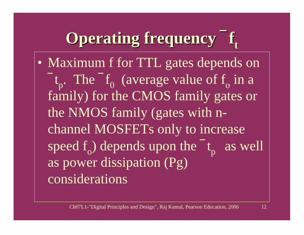
Operating frequency Operating frequency fftt• Maximum f for TTL gates depends on
tp. The f0 (average value of fo in a family) for the CMOS family gates or the NMOS family (gates with n-channel MOSFETs only to increase speed fo) depends upon the tp as well as power dissipation (Pg) considerations
Ch07L1-"Digital Principles and Design", Raj Kamal, Pearson Education, 2006 13
Outline
• Speed• Propagation delay • Operating frequency• Power dissipated per gate• Supply voltage levels• Operational voltage levels
Ch07L1-"Digital Principles and Design", Raj Kamal, Pearson Education, 2006 14
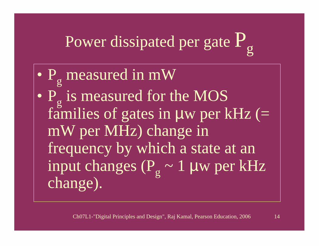
Power dissipated per gate Pg
• Pg measured in mW • Pg is measured for the MOS
families of gates in µw per kHz (= mW per MHz) change in frequency by which a state at an input changes (Pg ~ 1 µw per kHz change).
Ch07L1-"Digital Principles and Design", Raj Kamal, Pearson Education, 2006 15
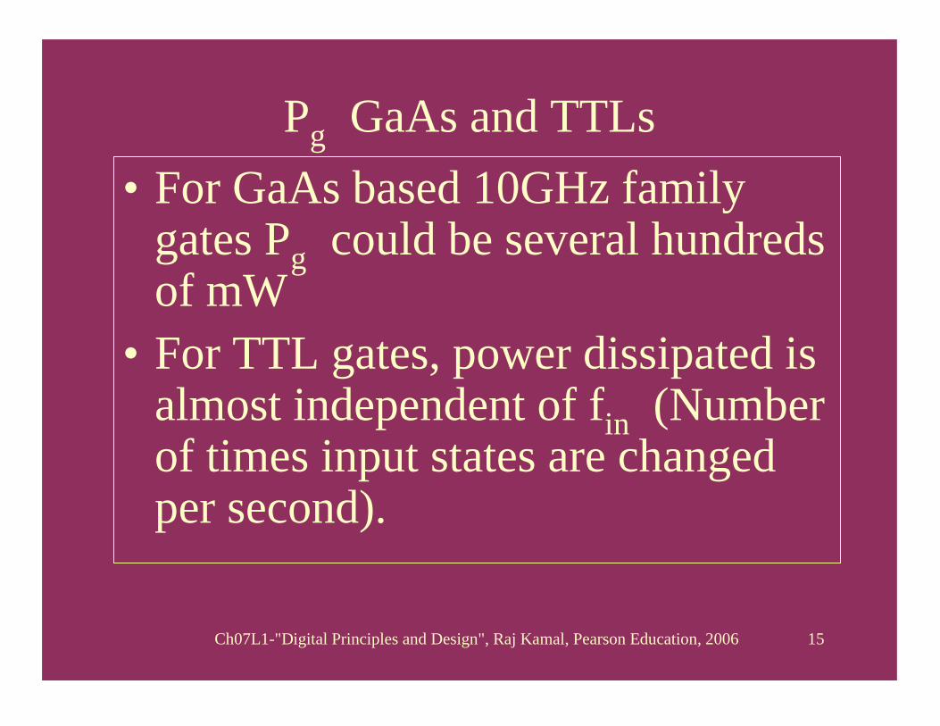
Pg GaAs and TTLs• For GaAs based 10GHz family
gates Pg could be several hundreds of mW
• For TTL gates, power dissipated is almost independent of fin (Number of times input states are changed per second).
Ch07L1-"Digital Principles and Design", Raj Kamal, Pearson Education, 2006 16
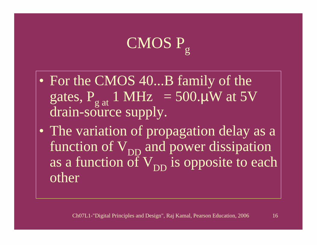
CMOS Pg
• For the CMOS 40...B family of the gates, Pg at 1 MHz = 500.µW at 5V drain-source supply.
• The variation of propagation delay as a function of VDD and power dissipation as a function of VDD is opposite to each other
Ch07L1-"Digital Principles and Design", Raj Kamal, Pearson Education, 2006 17
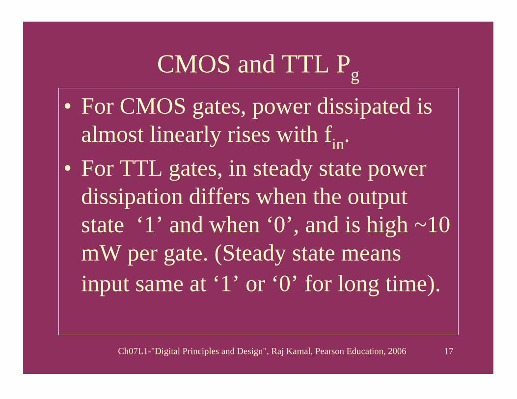
CMOS and TTL Pg
• For CMOS gates, power dissipated is almost linearly rises with fin.
• For TTL gates, in steady state power dissipation differs when the output state ‘1’ and when ‘0’, and is high ~10 mW per gate. (Steady state means input same at ‘1’ or ‘0’ for long time).
Ch07L1-"Digital Principles and Design", Raj Kamal, Pearson Education, 2006 18
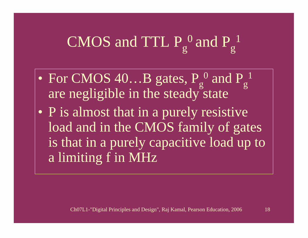
CMOS and TTL Pg0 and Pg
1
• For CMOS 40…B gates, Pg0 and Pg
1
are negligible in the steady state• P is almost that in a purely resistive
load and in the CMOS family of gates is that in a purely capacitive load up to a limiting f in MHz
Ch07L1-"Digital Principles and Design", Raj Kamal, Pearson Education, 2006 19
Outline
• Speed• Propagation delay • Operating frequency• Power dissipated per gate• Supply voltage levels• Operational voltage levels
Ch07L1-"Digital Principles and Design", Raj Kamal, Pearson Education, 2006 20
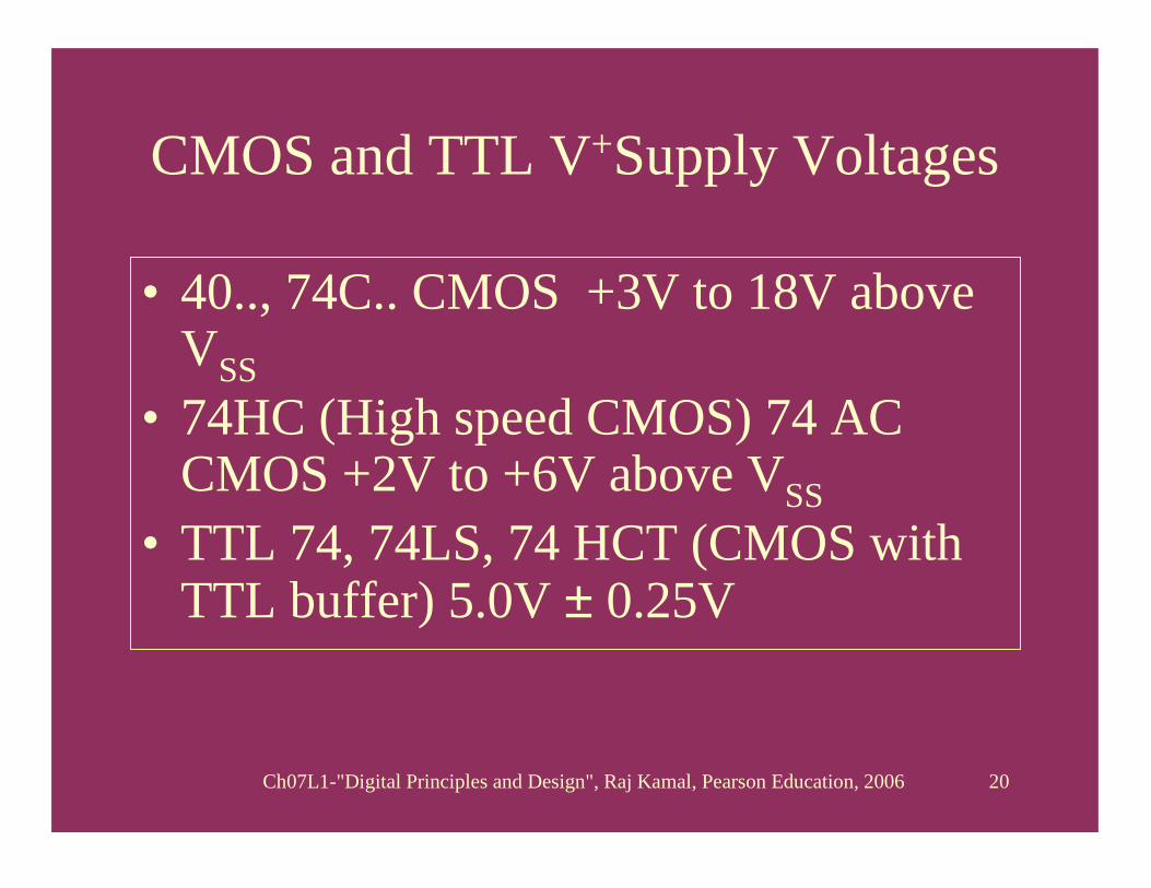
CMOS and TTL V+Supply Voltages
• 40.., 74C.. CMOS +3V to 18V above VSS
• 74HC (High speed CMOS) 74 AC CMOS +2V to +6V above VSS
• TTL 74, 74LS, 74 HCT (CMOS with TTL buffer) 5.0V ± 0.25V
Ch07L1-"Digital Principles and Design", Raj Kamal, Pearson Education, 2006 21
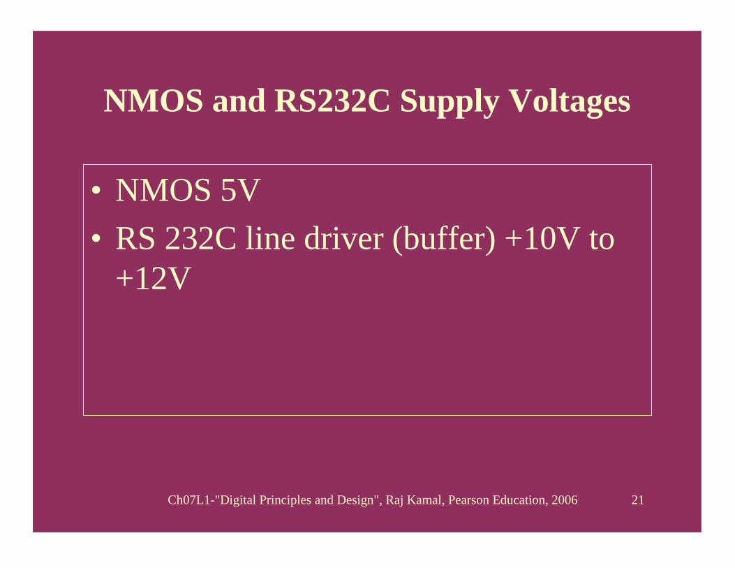
NMOS and RS232C Supply Voltages
• NMOS 5V • RS 232C line driver (buffer) +10V to
+12V
Ch07L1-"Digital Principles and Design", Raj Kamal, Pearson Education, 2006 22
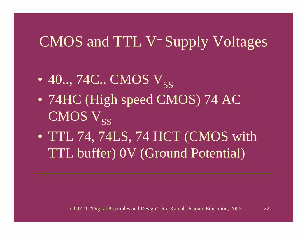
CMOS and TTL V– Supply Voltages
• 40.., 74C.. CMOS VSS
• 74HC (High speed CMOS) 74 AC CMOS VSS
• TTL 74, 74LS, 74 HCT (CMOS with TTL buffer) 0V (Ground Potential)
Ch07L1-"Digital Principles and Design", Raj Kamal, Pearson Education, 2006 23
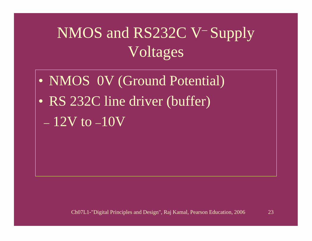
NMOS and RS232C V– Supply Voltages
• NMOS 0V (Ground Potential)• RS 232C line driver (buffer) – 12V to –10V
Ch07L1-"Digital Principles and Design", Raj Kamal, Pearson Education, 2006 24
Outline
• Speed• Propagation delay • Operating frequency• Power dissipated per gate• Supply voltage levels• Operational voltage levels
Ch07L1-"Digital Principles and Design", Raj Kamal, Pearson Education, 2006 25
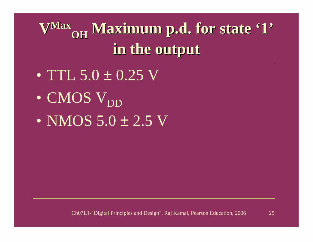
VVMaxMaxOHOH Maximum p.d. for state Maximum p.d. for state ‘‘11’’
in the outputin the output• TTL 5.0 ± 0.25 V• CMOS VDD
• NMOS 5.0 ± 2.5 V
Ch07L1-"Digital Principles and Design", Raj Kamal, Pearson Education, 2006 26
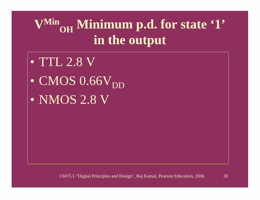
VMinOH Minimum p.d. for state ‘1’
in the output
• TTL 2.8 V• CMOS 0.66VDD
• NMOS 2.8 V
Ch07L1-"Digital Principles and Design", Raj Kamal, Pearson Education, 2006 27
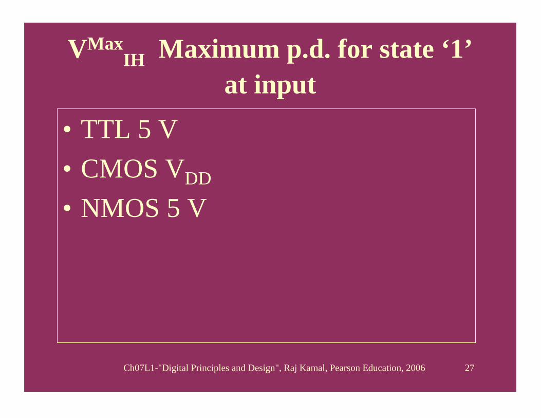
VMaxIH Maximum p.d. for state ‘1’
at input• TTL 5 V• CMOS VDD
• NMOS 5 V

Ch07L1-"Digital Principles and Design", Raj Kamal, Pearson Education, 2006 28
VMinIH Minimum p.d. for state ‘1’
at the input• TTL 2.4 V• CMOS 0.66VDD
• NMOS 2.4 V

Ch07L1-"Digital Principles and Design", Raj Kamal, Pearson Education, 2006 29
VVMaxMaxOLOL Maximum p.d. for state Maximum p.d. for state ‘‘00’’
in the outputin the output• TTL 0.4 V• CMOS 0.33VDD
• NMOS 0.4 V
Ch07L1-"Digital Principles and Design", Raj Kamal, Pearson Education, 2006 30
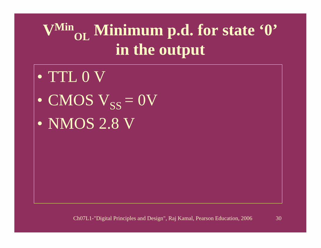
VMinOL Minimum p.d. for state ‘0’
in the output
• TTL 0 V• CMOS VSS = 0V• NMOS 2.8 V
Ch07L1-"Digital Principles and Design", Raj Kamal, Pearson Education, 2006 31
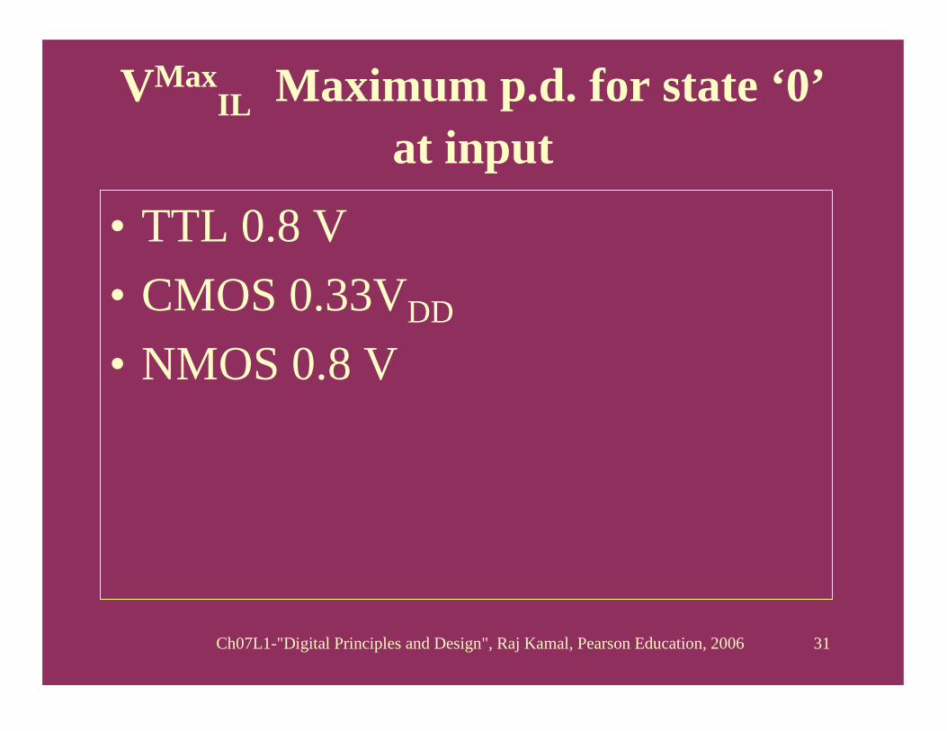
VMaxIL Maximum p.d. for state ‘0’
at input• TTL 0.8 V• CMOS 0.33VDD
• NMOS 0.8 V
Ch07L1-"Digital Principles and Design", Raj Kamal, Pearson Education, 2006 32
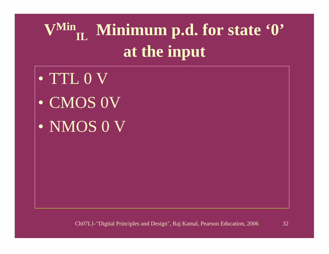
VMinIL Minimum p.d. for state ‘0’
at the input• TTL 0 V• CMOS 0V• NMOS 0 V
Ch07L1-"Digital Principles and Design", Raj Kamal, Pearson Education, 2006 33
Summary
Ch07L1-"Digital Principles and Design", Raj Kamal, Pearson Education, 2006 34
• We learnt characteristic parameters, which are considered when interfacing a gate
Ch07L1-"Digital Principles and Design", Raj Kamal, Pearson Education, 2006 35
End of Lesson 1 on CHARACTERISTIC
PARAMETERS
Ch07L1-"Digital Principles and Design", Raj Kamal, Pearson Education, 2006 36
THANK YOU