
CHAPTER 6 LOW-COMPLEXITY DESIGN FOR...
20
89 CHAPTER 6 LOW-COMPLEXITY DESIGN FOR FOLDED 2-D DWT 6.1 Introduction There is a growing demand for wireless and hand-held communication devices due to its portability and easy to use in remote locations. Many of these devices are run by limited battery power and enabled with multimedia applications. These devices implement many signal processing and communication algorithms to improve the quality of the output. In many cases, these devices need real-time processing speed to deliver better performance. However, most of the portable devices are constrained with area and power. It is well known that multimedia signals are stored or transmitted in compressed form to save time and resource. Efficient coding standards like MP3, JPEG2000 and MPEG-4 are developed to deal with multimedia signals. Due to remarkable advantage of DWT over DCT, the transform coder of MP3, JPEG2000 and MPEG-4 are adopted DWT. The transform coder of JPEG2000 uses wavelet filters 5/3 and 9/7 as default filter for lossless and lossy compression [Skodars et al. (2001)]. Most of the images are lossy-compressed except selected biomedical images, to achieve lower bit-rate. In recent year, portable and mobile devices are enabled with audio and video processing applications, wireless communication and internet application. Mobile devices need to support increasingly diverse and more sophisticated function in the coming years. It requires high speed, low power and low-complexity digital hardware to deliver superior performance under resource constrained environment. Throughput of digital hardware can be increased by introducing higher level of concurrency (parallel and / pipelining). Arithmetic complexity of the digital system increases proportionality with the level of concurrency. Multiplier is the most complex component in an arithmetic unit and it consumes major part of the area and power of a digital hardware. Therefore, limited number of arithmetic unit can be accommodated in the resource constrained devices which may limit the throughput. Recently various schemes have been proposed for multiplierless implementation of DWT based on convolution scheme or lifting scheme for low-complexity solution [Alam et al. (2003); Al-Haj (2005); Cao et al. (2006); Martina and Masera (2006); Martina and Masera
Transcript of CHAPTER 6 LOW-COMPLEXITY DESIGN FOR...

89
CHAPTER 6
LOW-COMPLEXITY DESIGN FOR FOLDED 2-D DWT
6.1 Introduction
There is a growing demand for wireless and hand-held communication devices due to
its portability and easy to use in remote locations. Many of these devices are run by limited
battery power and enabled with multimedia applications. These devices implement many
signal processing and communication algorithms to improve the quality of the output. In
many cases, these devices need real-time processing speed to deliver better performance.
However, most of the portable devices are constrained with area and power. It is well known
that multimedia signals are stored or transmitted in compressed form to save time and
resource. Efficient coding standards like MP3, JPEG2000 and MPEG-4 are developed to deal
with multimedia signals. Due to remarkable advantage of DWT over DCT, the transform
coder of MP3, JPEG2000 and MPEG-4 are adopted DWT. The transform coder of JPEG2000
uses wavelet filters 5/3 and 9/7 as default filter for lossless and lossy compression [Skodars et
al. (2001)]. Most of the images are lossy-compressed except selected biomedical images, to
achieve lower bit-rate.
In recent year, portable and mobile devices are enabled with audio and video
processing applications, wireless communication and internet application. Mobile devices
need to support increasingly diverse and more sophisticated function in the coming years. It
requires high speed, low power and low-complexity digital hardware to deliver superior
performance under resource constrained environment. Throughput of digital hardware can be
increased by introducing higher level of concurrency (parallel and / pipelining). Arithmetic
complexity of the digital system increases proportionality with the level of concurrency.
Multiplier is the most complex component in an arithmetic unit and it consumes major part of
the area and power of a digital hardware. Therefore, limited number of arithmetic unit can be
accommodated in the resource constrained devices which may limit the throughput.
Recently various schemes have been proposed for multiplierless implementation of
DWT based on convolution scheme or lifting scheme for low-complexity solution [Alam et
al. (2003); Al-Haj (2005); Cao et al. (2006); Martina and Masera (2006); Martina and Masera

90
(2007); Jing and Bin (2007); Longa et al. (2008); Acharyya et al. (2009)]. The shift-add and
the memory based designs are the most common techniques used for multiplierless
realization of DWT structure. Both these techniques have some advantages and
disadvantages. The shift-add based structure involves more adder compared with the memory
based structure, while the later one involves extra read only memory (ROM) words to store
the partial results. Using common sub expression elimination technique [Hartley (1996)] the
adder complexity of the shift-add structure may be optimized, but it involves irregular data
flow and involves higher cycle period compared with the memory based structure. Although,
the memory based structure involves extra memory cells, in recent years, it gained popularity
for high throughput, multiplierless processing with increased regularity, which results in cost
effective and area-time efficient VLSI structures [Guo et al. (1992); Chiper et al. (2005);
Meher et al. (2008b); Allread et al. (2005)].
Direct ROM and the distributed arithmetic (DA) are the two basic techniques are used
for memory based design. In direct ROM based implementation, constant multiplication
operation can be performed using ROM based look-up-table (LUT) of size 2L, which store the
pre-computed all possible product values of the input samples of word length size L. In this
case the multiplication operation is simply replaced with ROM memory read operation and
that results low cycle period compared to the multiplier accumulator based designs. Inner
product of two K-points vectors can be expressed in DA [White (1989)]. In DA, 2K possible
pre-computed partial inner product values are stored in a ROM based LUT of size 2K, where
K is the length of the input vector. Both direct ROM and DA-based techniques have some
advantages and disadvantages. The ROM based implementation involves less memory
complexity compared with the DA-based technique when the word length is less than the size
of the input vector, while the later has the less memory complexity otherwise. The time
complexity of the DA-based structures is independent of the size of the input vector and
depends on the word length, while in the case of ROM based structures, the time complexity
depends on the size of the input vector and independent on the word length. Both direct
memory and DA-based designs are suitable for multiplierless realization of DWT. But, we
find that DA is more suitable for DWT, since small sizes filters are used for wavelet
decomposition and the required bit precision is more than 12-bit for various applications.
Therefore, we have chosen DA-based design approach to derive a low-complexity hardware
component for DWT.

91
Several multiplierless design schemes have been suggested by various authors in
recent years. Few of them are discussed here. Cao et al. (2006) have derived a DA structure
for 1-D DWT based on new DA algorithm suggested by [Pan et al. (1999)] and subsequently
applied compression technique to reduce adder complexity of the structure. Martina and
Masera (2007) have approximated 9/7 filter coefficients and expressed 9/7 filter outputs in
terms of 5/3 filter output using common multiple constant method. They have also suggested
a multiplierless structure to compute both 5/3 and 9/7 filters based DWT. The structure of
[Martina and Masera (2007)] involves significantly less adders then the earlier structures.
Longa et al. (2008) have suggested a LUT-less DA design for implementation of DWT core.
They have implemented DA-LUT using adders and multiplexers (MUXes). However, the
adder complexity of structure is significantly higher than the previous multiplierless
structures. Recently, Mohanty and Meher (2009) have proposed a DA-based architecture for
implementation of 1-D DWT. The structure of [Mohanty and Meher (2009)] is the most
efficient amongst the existing DA structures. However, the hardware and time complexity of
[Mohanty and Meher (2009)] could be optimized further to make it more efficient structure.
Keeping the above facts in mind, we have suggested a systematic design approach for
derivation of a low-complexity area efficient arithmetic core for the folded 2-D DWT using
9/7 wavelet filters. The following design steps are considered:
a) Derive an optimized DA-based structure for 1-D DWT.
b) Optimize 1-D DWT structure as row and column processor to build the arithmetic
core of the folded 2-D DWT structure.
c) Consider both line-based and parallel data access schemes to find the most
appropriate multiplierless structure for folded 2-D DWT.
The key ideas we have used to optimize the DA-based 1-D DWT structure are:
To generate bit-slices using carry save full adder (CSFA).
To accumulate partial results using carry save accumulator (CSAC).
Using the proposed design scheme, we have derived DA-based structure for the folded 2-
D DWT. The rest of the Chapter is organized as follows: Mathematical formulation of DA-
based 1-D DWT is presented in Section 6.2. The proposed DA-based 1-D DWT structure is
discussed in Section 6.3. The proposed DA-based folded 2-D DWT structure is discussed in
Section 6.4. Hardware-time complexities and performance comparison of the proposed
structures are discussed in Section 6.5. The conclusion of Chapter is presented in Section 6.6.

92
6.2 Distributed Arithmetic Formulation of 1-D DWT
Inner product computation can be expressed by DA [White (1989)]. The DWT
formulation using convolution scheme given in (1.1) – (1.2) can be expressed by inner
product, where the lifting DWT formulation given in (1.7) – (1.12) cannot be expressed by
inner product. Although, convolution DWT demands more arithmetic resources than lifting
DWT, convolution DWT is considered to take the advantages of DA-based design. DA
formulation of convolution-based DWT using 9/7 biorthogonal filter is presented here.
According to (1.1) and (1.2), the 9/7 wavelet filter computation in convolution form is
expressed as
8
0( ) ( ) ( )l n
iu n h i s i
(6.1)
7
0( ) ( ) ( )h n
iu n g i r i
(6.2)
The low-pass filter coefficients {h(i)} and high-pass filter coefficients {g(i)} of the 9/7
wavelet filter satisfy the symmetry property. Therefore, the computation of DWT, with
symmetric filter coefficients of 9/7 filters, can be formulated as [Mohanty and Meher (2009)]
4
0( ) ( ) ( )l n
iu n h i s i
(6.3)
3
0( ) ( ) ( )h n
iu n g i r i
(6.4)
where,
(0) ( ) ( 6)nr x n x n (6.5)
(1) ( 1) ( 5)nr x n x n (6.6)
(2) ( 2) ( 4)nr x n x n (6.7)
(3) ( 3)nr x n (6.8)
(0) ( ) ( 8)ns x n x n (6.9)
(1) ( 1) ( 7)ns x n x n (6.10)

93
(2) ( 2) ( 6)ns x n x n (6.11)
(3) ( 3) ( 5)ns x n x n (6.12)
(4) ( 4)ns x n (6.13)
where uh(n) and ul(n) are, respectively, the high-pass and low-pass DWT coefficients, and
x(n) is the input signal. For simplicity, it is assumed the signal samples of sequences h(i), g(i),
rn(i) and sn(i) to be L-bit numbers in 2’s complement representation. Each of the intermediate
signals rn(i), for 0 ≤ i ≤ 3, of (6.4) may thus be expressed in expanded form as
1
01
( ) ( ( )) 2 ( ( ))L
ln n n l
lr i r i r i
(6.14)
Substituting (6.14) in (6.4) and rearranging the order of summation, (6.4) can be rewritten as
1 3 3
01 0 0
( ) ( )( ( )) 2 ( ) ( ( ))L
lh n l n
l i iu n g i r i g i r i
(6.15)
Equation (6.15) may otherwise be expressed as
1 3
0 0( ) ( )( ( )) 2
Ll
h l n li i
u n c g i r i
(6.16)
Where, cl = 1 for 1 ≤ l ≤ L-1 and cl = -1 for l = 0. Equation (6.16) can expressed in memory
read form
1
0( ) ( (( ) )) 2
Ll
h n ll
u n F b r
(6.17)
and similarly (6.3) also can be expressed as
1
0( ) ( (( ) )) 2
Ll
l n ll
u n F b s
(6.18)
where F(.) is memory read operation, and the bit-vectors are defined as
94
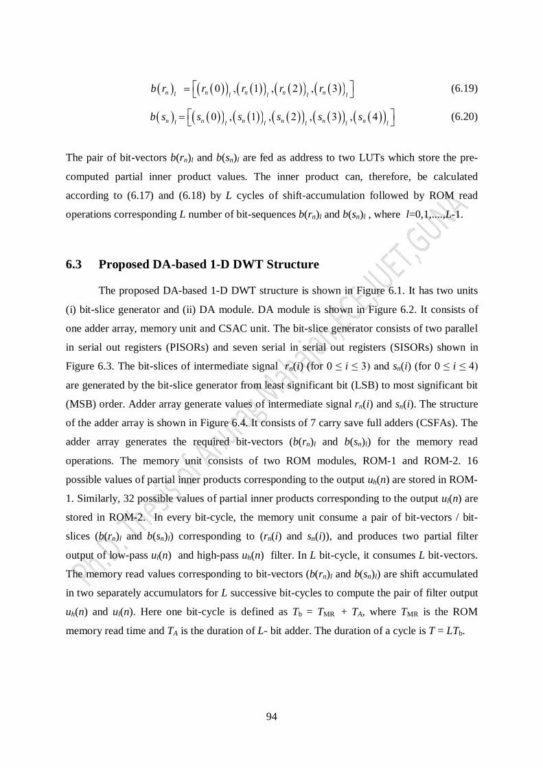
0 , 1 , 2 , 3 n n n n nl l l l lb r r r r r (6.19)
0 , 1 , 2 , 3 , 4n n n n n nl l l l l lb s s s s s s (6.20)
The pair of bit-vectors b(rn)l and b(sn)l are fed as address to two LUTs which store the pre-
computed partial inner product values. The inner product can, therefore, be calculated
according to (6.17) and (6.18) by L cycles of shift-accumulation followed by ROM read
operations corresponding L number of bit-sequences b(rn)l and b(sn)l , where l=0,1,....,L-1.
6.3 Proposed DA-based 1-D DWT Structure
The proposed DA-based 1-D DWT structure is shown in Figure 6.1. It has two units
(i) bit-slice generator and (ii) DA module. DA module is shown in Figure 6.2. It consists of
one adder array, memory unit and CSAC unit. The bit-slice generator consists of two parallel
in serial out registers (PISORs) and seven serial in serial out registers (SISORs) shown in
Figure 6.3. The bit-slices of intermediate signal rn(i) (for 0 ≤ i ≤ 3) and sn(i) (for 0 ≤ i ≤ 4)
are generated by the bit-slice generator from least significant bit (LSB) to most significant bit
(MSB) order. Adder array generate values of intermediate signal rn(i) and sn(i). The structure
of the adder array is shown in Figure 6.4. It consists of 7 carry save full adders (CSFAs). The
adder array generates the required bit-vectors (b(rn)l and b(sn)l) for the memory read
operations. The memory unit consists of two ROM modules, ROM-1 and ROM-2. 16
possible values of partial inner products corresponding to the output uh(n) are stored in ROM-
1. Similarly, 32 possible values of partial inner products corresponding to the output ul(n) are
stored in ROM-2. In every bit-cycle, the memory unit consume a pair of bit-vectors / bit-
slices (b(rn)l and b(sn)l) corresponding to (rn(i) and sn(i)), and produces two partial filter
output of low-pass ul(n) and high-pass uh(n) filter. In L bit-cycle, it consumes L bit-vectors.
The memory read values corresponding to bit-vectors (b(rn)l and b(sn)l) are shift accumulated
in two separately accumulators for L successive bit-cycles to compute the pair of filter output
uh(n) and ul(n). Here one bit-cycle is defined as Tb = TMR + TA, where TMR is the ROM
memory read time and TA is the duration of L- bit adder. The duration of a cycle is T = LTb.

95
Figure 6.1: Proposed DA-based 1-D DWT structure.
Figure 6.2: Structure of DA module.
x(2n)l
Bit-slice generator
DA module
x(2n)
uh(n) ul(n)
x(2n-1)
x(2n -1)l. . . x(2n-7)l x(2n-8)l
b(rn)l b(sn)l
F(b(rn)l) F(b(sn)l)
uh(n) ul(n)
Adder array
x(2n -1)l
. . .
x(2n -7)lx(2n)l
ROM-1(16 words)
ROM-2(32 words)
Memoryunit
x(2n -8)l
CSAC CSACCSACunit

96
Figure 6.3: Structure of bit-slice generator.
Figure 6.4: Structure of adder array.
For fast accumulation of the partial results, CSAC is used in place of normal
accumulators. The structure of the CSAC is shown in Figure 6.5. It receives one partial
output in every bit-cycle from the ROM unit. The partial results corresponding to L
successive bit-cycles are shift accumulated in the carry save adder (CSA) of the CSAC.
During L-th bit-cycle of every cycle, the final sum and carry words are flushed out from the
CSA and accumulated in a separate ripple carry adder (RCA). Once the sum and carry words
are flushed out from the CSA, the contents of register R1 and R2 are cleared immediately in
the next bit-cycle.
PISORx(2n)
PISORx(2n-1)
SISOR SISOR SISOR SISOR
SISOR SISOR SISOR
x(2n)l x(2n-1)l x(2n-2)l x(2n-3)l x(2n-4)l x(2n-5)l x(2n-6)l x(2n-7)l x(2n-8)l
CSFA
CSFA
x(2n
) l
rn(0)l
rn(1)l
rn(2)l
rn(3)l
sn(4)l
sn(3)l
sn(2)lsn(1)l
sn(0)l
Address port of ROM-2 of MU
x(2n
-2)
l
x(2n
-5)
l
x(2n
-6)
l
x(2n
-4)
l
CSFA
CSFA
CSFA
CSFA
CSFA
Address port of ROM-1 of MUx(
2n -
8)l
x(2n
-3)
l
x(2n
-1)
l
x(2n
-7)
l

97
Figure 6.5: Structure of carry save accumulator (CSAC), where duration of CLK1 is equal to one bit-period
(Tb), and duration of CLK2 is equal to one cycle period (T).
During the L-th bit-cycle of every cycle, the bit-vectors (b(rn)l and b(sn)l) contains the
sign bits. The memory read value is subtracted from the previous accumulated result during
the L-th bit-cycle. The subtraction operation is performed in the same CSA using a sign
control circuit. The sign control circuit is comprised of an array of L 2-input XOR gates. The
operation of the sign control circuit of CSAC is controlled by the control signal 'CTR', where
CTR is defined for one cycle as {(L-1) zeros followed by 1}. Control signal 'CTR', is XORed
with the memory read values through the sign control and at the same time it is added with
the accumulator content with the carry-in (Cin) input of the CSA. The control signal 'CTR' is
also used to select the outputs of the demultiplexer (DMUX) and to clear the registers (R1,
R2). Both CSA and RCA work in separate pipeline stages. A pair of DWT coefficients (uh(n),
ul(n)) are obtained from the structure in every cycle.
CTRSign Control
CSA
DM
UX
R1
>>1
CLK1
CTR
x(n)
Cin
CLR
RCA
R3
CLK2D
MU
X
CTR
R2 CLK1
R4
CLK2
y(n)

98
6.4 Proposed DA-Based Folded 2-D DWT Structure
Transposition memory size depends mainly on the type of data access scheme adopted
to feed the input data. Line-based and parallel data access schemes are more commonly used
in 2-D DWT structures to reduce the transposition memory. In this Section, DA-based 2-D
DWT structures are derived using both these data access schemes.
6.4.1 Using Line-Based Data Access Scheme
The proposed DA-based 2-D DWT structure using line-based data access scheme
refer to architecture-1 is shown in Figure 6.6. It consists of multiplexer (MUX) unit, bit-slice
generator, row-processor, column-processor, transposition memory, input buffer and frame
buffer. In every cycle, MUX unit of the proposed architecture-1 receives 2 samples either
from the input buffer or from the frame buffer in a row-wise manner as discussed in Section
2.1.1. MUX unit consists of two word-level multiplexers required to select the required DWT
level. Samples of particular DWT level selected by the multiplexer are fed to the bit-slice
generator. The structure of the bit-slice generator is identical to the bit-slice generator of
Figure 6.3. Bit-slices generated by the bit-slice generator are fed to row-processor in LSB to
MSB order in a period of L bit-cycles, where L bit-cycles constitute one cycle. The proposed
DA module for 1-D DWT of Figure 6.2 is used as row-processor and column-processor for
the proposed architecture–1. In each cycle, row-processor receives L bit-slices and calculates
a pair of intermediate components one low-pass (ul(m,n)) and one high-pass (uh(m,n)). The
row-processor of architecture-1 generates intermediate components in row-wise. These
intermediate components are fed to transposition memory to feed the intermediate
components to the column-processor in column-wise. Transposition memory consists of one
PISOR, one MUX, one shift register (SR) of (N/2) words and 8 serial in serial out shift
registers (SISOSRs) of N words each. Structure of transposition memory is shown in Figure
6.7. Transposition memory provides the necessary column delay as well as introduces
embedded down sampling for the column DWT. The transposition memory generates bit-
slices of 9-point low-pass intermediate vector ul(m,n) and 7-point high-pass intermediate
vector uh(m,n) in time multiplexed form such that it generates the bit-slices of ul(m,n) in even
set of ( NL/2) bit-cycles and of uh(m,n) in during odd set of (NL/2) bit-cycles. The bit-slices
generated by the transposition memory are fed to the column-processor. Column-processor
computes a pair of DWT components of the subband matrices (C, D) or (B, A) in every

99
cycle. The entire DWT of the first-level is computed in (MN/2) cycles. The low-low subband
components of 1-level (A1) are sent to frame buffer for computation of multilevel DWT using
folded scheme.
Figure 6.6: DA-based 2-D DWT structure using line-based data access scheme (architecture-1).
Multiplexer unit
Bit-slice generator
Row-processor(DA module)
Transposition memory
ul(m,n)uh(m,n)
9 bits
Column-processor(DA module)
9 bits
DMUXDMUX
1A j1B j1C j1D j
x(m,2n)x(m,2n-1)
Frame buffer (size 5M
N/16)
Input buffer(size MN)

100
Figure 6.7: Structure of transposition memory of architecture-1.
6.4.2 Using Parallel Data Access Scheme
The proposed DA-based 2-D DWT structure using parallel data access scheme refer
to architecture-2 is shown in Figure 6.8. It consists of one MUX unit, 2 bit-slice generators
(one for row-processor and one for column-processor), one row-processor, one column-
processor, one input buffer and one frame buffer. In every cycle, MUX unit of the proposed
architecture-2 receives 9 samples either from the input buffer or from the frame buffer. These
nine samples are prepared from a set of 9 consecutive columns of the input matrix such that
adjacent sets of columns are overlapped by 7 columns as discussed in Section 2.1.2. The
MUX unit consists of nine word-level MUXes. Samples of particular DWT level are selected
by the MUX unit are fed to the bit-slice generator. Bit-slice generator consists of 9 PISORs.
The bit-slices generated by the bit-slice generator are fed to row-processor in LSB to MSB
order in L bit-cycles, where L bit-cycles constitute one cycle. The proposed DA module for 1-
D DWT shown in Figure 6.2 is used as row-processor and column-processor in the proposed
architecture-2. In each cycle, row-processor receives L bit-slices and calculates one low-pass
(ul(m,n)) and one high-pass (uh(m,n)) intermediate components. Since, intermediate
components generated by the row-processor in successive cycles are belongs to same column.
These intermediate components are processed by the column-processor without data
transposition.
ul(m,n)
Multiplexer
SR
SISOSR
SISOSR
PISO
SISOSR
SISOSR
SISOSR
SISOSR
SISOSR
SISOSR
uh(m,n)
u(m,n)l u(m-1,n)l u(m-2,n)l u(m-3,n)l u(m-4,n)l u(m-5,n)l u(m-6,n)l u(m-7,n)l u(m-8,n)l

101
Figure 6.8: DA-based 2-D DWT structure using parallel data access scheme (architecture -2).
Multiplexer unit
Bit-slice generator
Row-processor(DA module)
Bit –slice generatorfor column processor
ul(m,n)uh(m,n)
9 bits
Column-processor(DA module)
9 bits
DMUXDMUX
1A j1B j1C j1D j
ameFram
ebuffer (5MN/16)
Input buffer(size MN)
Overhead (size 10.5 N) Overhead (size 7N )
9 Samples
9 Samples

102
Figure 6.9: Bit-slice generator of column processor.
The intermediate output (ul(m,n) and uh(m,n)) generated by the row-processor in
column-wise manner is fed to the bit-slice generator of column-processor. Bit-slice generator
for column-processor consists of 2 PISORs and 17 SISORs. Structure of bit-slice generator is
shown in Figure 6.9. Bit-slice generator also provides the necessary down-sampled filter
computation. The bit-slices generated by the bit-slice generator are fed to the column-
processor column-wise. Column-processor computes a pair of DWT components of the
subband matrices (C, D) or (B, A) in every cycle. The entire DWT of the first-level is
computed in (MN/2) cycles. The low-low subband components of 1-level (A1) are sent to
frame buffer for computation of multilevel DWT using folded scheme. Using parallel data
access, transposition memory is avoided but that introduces some additional complexity to
the frame buffer of the folded 2-D DWT and input buffer to provide the necessary
overlapping of columns delay. The control circuit required for the operation of the frame
buffer is, therefore, quite complex [Mohanty and Meher (2013)].
6.5 Hardware-Time Complexities and Performance Comparison
6.5.1 Hardware and Time Complexities
The proposed DA-based 1-D DWT structure is comprised of one bit-slice generator
and one DA module. Bit-slice generator consist of 2 PISORs and 7 SISORs. DA module is
consisting of one adder array, one memory unit and one CSAC unit. The adder array is
comprised of 7 CSFAs, where the memory unit is comprised of 48 ROM words. The CSAC
unit is comprised of 2 L-bit CSAs, 2 L-bit RCAs, 8 registers (L-bit), 4 1:2 DMUX (word-
level) and 2L 2-input XOR gates. Besides this, it requires 9 D flip-flops and 2 registers for
pipelining. The proposed DA-based 1-D DWT structure, therefore, requires 2 L-bit RCAs,
(2L + 7) full adders, 19 registers, 18 D flip-flops, 4 DMUXes (word-level), 2L 2-input XOR
PISOR SISOR
SISOR
MUX
SISOR
SISOR
MUX
SISOR
SISOR
MUX
SISOR
SISOR
MUX
SISOR
SISOR
MUX
SISOR
SISOR
MUX
SISOR
SISOR
MUX
SISOR
SISOR
MUX
SISOR
MUX
PISOR
ul(m,n)
uh(m,n)
u(m,n)l u(m-1,n)l u(m-2,n)l u(m-3,n)lu(m-4,n)l u(m-5,n)l u(m-6,n)l u(m-7,n)l u(m-8,n)l

103
gates, 48 ROM words and, calculates a pair of DWT coefficient in every cycle, where one
cycle equal to L bit-cycles and one bit-cycle Tb = max(TMR ,TFA).
Proposed architecture-1 for 2-D DWT consists of MUX unit, bit-slice generator,
transposition memory, 2 numbers of DA module used as row-processor and column-
processor and one frame buffer. MUX unit consists of 2 word-level MUXes. Bit-slice
generator of row-processor consists of 2 PISORs and 7 SISORs. Transposition memory
consists of one PISOR, one SR of (N/2) words, 8 SISOSRs of N words each and one word-
level MUXes. The frame buffer involves (5MN/16) RAM words. Besides this, it requires 2
DMUXes. Proposed architecture-1, therefore, requires 4 L-bit RCAs, (4L + 14) full adders,
30 registers, 36 D flip-flops, one SR of (N/2) words, 8N SISOSRs words, 13 MUXes /
DMUXes (word-level), 4L 2-input XOR gates, 96 ROM words and frame buffer of size
(5MN/16) RAM words. It processes 2 samples in every cycle and requires (MN/2) cycles to
compute 1-level 2-D DWT of an image of size (M × N), where one cycle is equal to L bit-
cycles and one bit-cycle Tb = max(TMR, TFA). The proposed architecture-1 takes 2MN(1-2-2J)/3
cycles to compute J levels 2-D DWT.
Proposed architecture-2 for 2-D DWT consists of one MUX unit, 2 bit-slice
generators, 2 numbers of DA modules used as row-processor and column-processor, and one
frame buffer. MUX unit consist of 9 word-level MUXes. Bit-slice generator of row-processor
consists of 9 PISORs. Bit-slice generator of column-processor consists of 2 PISORs, 17
SISORs and 9 bit-level MUXes. The frame buffer involves (5MN/16 + 10.5N) RAM words.
Besides this, it requires 2 DMUXes. Proposed architecture-2, therefore, requires 4 L-bit
RCAs, (4L + 14) full adders, 48 registers, 36 D flip-flops, 19 MUXes / DMUXes (word-
level), 9 bit-level MUXes, 4L 2-input XOR gates, 96 ROM words and frame buffer of size
(5MN/16 + 10.5N) RAM words. It processes 2 samples in every cycle and requires (MN/2)
cycles to compute 1-level 2-D DWT of an image of size (M × N), and where one cycle is
equal to L bit-cycles and one bit-cycle Tb = max(TMR ,TFA). It takes 2MN(1-2-2J) / 3 cycles to
compute J levels 2-D DWT.
6.5.2 Performance Comparison
The hardware and time complexity of the proposed and the existing multiplierless 1-D
DWT structures are listed in Table 6.1 for comparison. It is found from Table 6.1 that, the

104
structure of [Mohanty and Meher (2009)] is the most efficient among the existing structures
as it involves least number of adders and offers higher throughput due to its small cycle
period. Compared with the structure of [Mohanty and Meher (2009)], the proposed structure
involves 7 less adders, 7 less DMUXes/MUXes, extra (2L + 7) full adders and 8 more
registers and calculate DWT coefficients nearly L times higher rate.
Table 6.1: General comparison of hardware and time complexities of the proposed and the existing
multiplierless 1-D DWT structure using 9/7 wavelet filter
LEGEND: ADD: Adder, FA: Full adder, MUX: Multiplexer, DMUX: Demultiplexer, CP: Cycle period, CT:
Computation time.
The hardware and time complexity of the proposed DA-based 2-D DWT architectures
(architecture-1 and architecture-2) and the existing multiplier based 2-D DWT structures of
[Huang et al. (2005b); Meher et al. (2008a)] are listed in Table 6.2 in terms of multiplier,
adder, on-chip memory, frame buffer, full adder, ROM and time-complexity in terms of cycle
period. On-chip memory represents the pipeline/data registers and line buffer words required
by each design. Both the proposed DA-based structures involve same logic components (full
adder, ROM, Adder) but they differ by on-chip memory and frame buffer. Compared with
proposed architecture-1, proposed architecture-2 requires nearly 8.5N less on-chip memory
words, but it requires 10.5N more frame buffer words and 7N input buffer words. Compared
with the line-based structure of [Huang et al. (2005b)], the proposed DA-based architecture-1
does not involve any multiplier, but it requires extra (4L + 14) full adders, extra 4L 2-input
Structures ADD FAMUX/
DMUX
ROM
wordsRegister CP CT
Alam et al. (2003) 43 0 0 0 9 6TA 3N TA
Cao et al. (2006) 27 0 0 0 9 6TA 6N TA
Martina and Masera (2007) 19 0 8 0 9 6TA 6N TA
Longa et al. (2008) 35 0 40 0 9 6TA 6N TA
Mohanty and Meher (2009) 9 0 11 48 11 L(TMR + TA) LNT/2
Proposed
[Mahajan and Mohanty (2010b)]2 (2L+7) 4 48 19 L{max(TMR, TFA)} LNT/2

105
XOR gates, extra 96 ROM words. It involves 24 less adders, nearly same on-chip memory
words, same frame buffer words and involves more cycle period. Compared with parallel
data access scheme based structure of [Meher et al. (2008a)], the proposed DA-based
architecture-2 does not involve any multiplier but it requires extra (4L + 14) full adders, extra
4L 2-input XOR gates, extra 96 ROM words. It involves 24 less adders, nearly same on-chip
memory words, same frame buffer words and involves more cycle period. For resource
constrained application, proposed architecture-2 is better than proposed architecture-1, since
it requires less on-chip memory.
Table 6.2: General comparison of hardware and time complexities of the proposed structure and the existing
structures for convolution based 2-D DWT using 9/7 wavelet filter
LEGEND: MULT: Multiplier, ADD: Adder, FA: Full adder, FB: Frame buffer, CP: Cycle period.
6.5.3 Synthesis Result and Discussion
The proposed DA-based 1-D DWT structure and structures of [Mohanty and Meher
(2009); Martina and Masera (2007] are coded in VHDL. For synthesis of proposed and
existing design, 8-bit input signal and 12-bit intermediate and output signals are assumed.
The designs are synthesized by Synopsys Design Compiler using 90 nm TSMC CMOS
library. The area and data arrival time (DAT) reported by the Design Compiler are listed in
Table 6.3 for comparison. The proposed DA-based 1-D DWT structure [Mahajan and
Mohanty (2010b)] involves 11% less area and 35% less cycle period than the structure of
[Mohanty and Meher (2009)]. Compared with the adder based design of [Martina and Masera
Structures Data access scheme MULT ADD
On-chip
in wordsFA
ROM
words
FB
in wordsCP
Huang et al. (2005b) Line-based 18 28 8.5N + 27 0 0 5MN/16 TM + TA
Meher et al. (2008a) Parallel data 18 28 37 0 0 5MN/16 + 10.5N TM
Proposed
Architecture-1Line-based 0 4 8.5N + 30 (4L + 14) 96 5MN/16 L{max(TMR,TFA)}
Proposed
Architecture-2Parallel data 0 4 48 (4L + 14) 96 5MN/16 + 10.5N L{max(TMR,TFA)}

106
(2007], the proposed DA-based 1-D DWT structure [Mahajan and Mohanty (2010b)]
involves 36% less area and 82% more cycle period.
Table 6.3: Synthesis results of the proposed and existing multiplierless 1-D DWT structure using 9/7 wavelet
filter
LEGEND: DAT: Data arrival time, CP: Cycle period.
The proposed architecture-1 for 2-D DWT involves 17 line buffer of size (N/2) each,
where N is image width. The complexity of line buffer is significantly higher than the
complexity of arithmetic component. A line-based 2-D DWT structure involves line buffers
inside the core where a 2-D DWT structure based on parallel data-access does not involve
line buffers inside the core. When the core of the line-based and parallel data-access based 2-
D DWT structures are synthesized, then a marginal area saving is offered by the DA-based
design over the multipliers based design in case line-based 2-D DWT structure due to line-
buffer complexity which dominates the core complexity. On the other hand, the core of 2-D
DWT structure based on parallel data access offers a significant area saving when
implemented using DA design than the multiplier based design. Therefore, the proposed
architecture-2 and the similar existing multiplier based architecture of [Meher et al. (2008a)]
are considered for synthesis to observe the area saving offered by the DA design over the
multiplier based design. The core of the proposed architecture-2 and the core of the multiplier
based 2-D DWT structure of [Meher et al. (2008a)] are coded in VHDL. For synthesis of
proposed and existing design, 8-bit input signal and 12-bit intermediate and output signals are
assumed. All the designs are synthesized by Synopsys Design Compiler using 90 nm TSMC
CMOS library. The area and DAT reported by the Design Compiler are listed in Table 6.4 for
StructuresCore area
(µm2)
DAT
(ns)
CP
(ns)
Martina and Masera (2007) 22584.47 18.80 18.80
Mohanty and Meher (2009) 16280.61 8.80 52.8
Proposed
[Mahajan and Mohanty (2010b)]14439.33 5.69 34.14

107
comparison. As shown in Table 6.4, the proposed DA-based architecture-2 offers 43% area
saving than the multiplier based structure of [Meher et al. (2008a)], but it involves 2.7 times
more cycle period. Due to bit serial nature, the proposed DA-based structure has higher cycle
period than the corresponding multiplier based structure.
Table 6.4: Synthesis results of the proposed and existing 2-D DWT structure using 9/7 wavelet filter for DWT
levels J = 1
LEGEND: DAT: Data arrival time, CP: Cycle period.
6.6 Conclusion
In this Chapter, DA-based architecture for computation of 1-D DWT is presented.
CSFA is used to generate bit-vectors [Mahajan and Mohanty (2010a)] and CSAC is used to
accumulate the partial results to reduce the bit-clock period of the proposed DA-based 1-D
DWT structure [Mahajan and Mohanty (2010b)]. The proposed DA-based 1-D DWT
structure involves significantly less logic resources than the similar existing multiplierless
designs and, it has less bit-cycle period than others. Compared with the best of the existing
DA-based structure [Mohanty and Meher (2009)], the proposed structure involves 7 less
adders, 7 less DMUXes/MUXes, extra (2L + 7) full adders and 8 more registers and calculate
DWT coefficients nearly L times higher rate. Synthesis reports obtained from Synopsis
Design Compiler shows that, the proposed DA-based 1-D DWT structure [Mahajan and
Mohanty (2010b)] involves 11% less area and 35% less cycle period compared with the DA-
based structure of [Mohanty and Meher (2009)].
In this Chapter, two DA-based 2-D DWT architectures (architecture-1 and
architecture-2) are also proposed. The proposed DA-based 1-D DWT structure is used as row
StructuresCore area
(µm2)
DAT
(ns)
CP
(ns)
Meher et al. (2008a) 62850.01 14.65 14.65
Proposed architecture-2 35535.96 6.62 39.72

108
and column processor to construct a low-complexity arithmetic core of the folded 2-D DWT
structures. The proposed DA-based 2-D DWT architectures (architecture-1 and architecture-
2) involve the same logic components but they differ with on-chip memory size and frame
buffer size. The architecture-1 is based on line-scanning and the architecture-2 is based on
parallel data access scheme. The architecture-2 requires nearly 8.5N less on-chip memory
words than the architecture-1. But architecture-2 requires 10.5N extra frame buffer words and
7N input buffer words as an overhead than the architecture-1. Compared with the existing
multiplier based structure of [Huang et al. (2005b)], the proposed DA-based architecture-1
does not involve any multiplier. Instead of that, the proposed architecture–1 involves
(4L + 14) full adders, 4L XOR gates, 96 ROM words. It involves 24 less adders, nearly same
on-chip memory words, same frame buffer words and involves slightly higher cycle period.
Compared with the existing multiplier based structure of [Meher et al. (2008a)], the proposed
architecture-2 does not involve any multiplier. Instead of that it requires extra (4L + 14) full
adders, 4L XOR gates, 96 ROM words. It involves 24 less adders, nearly same on-chip
memory words, same frame buffer words and involves slightly higher cycle period. Synthesis
reports show that the proposed architecture-2 offers 43% area saving than the similar
multiplier based structure of [Meher et al. (2008a)] and it has 2.7 times higher cycle period.
The proposed DA-based structures have significantly less area complexity than the existing
designs. The proposed design is therefore, very much useful for low-complexity realization of
1-D and 2-D DWT for resource constrained DSP applications.