
Oxygen Oxygen Symbol and Atomic Number Symbol Atomic Number.

Hong Xiao, Ph. D. www2.austin.cc.tx.us/HongXiao/Book.htm 1
Chapter 5Thermal Processes
Hong Xiao, Ph. D.
Hong Xiao, Ph. D. www2.austin.cc.tx.us/HongXiao/Book.htm 2
Objective
• List four thermal processes
• Describe thermal process in IC fabrication
• Describe thermal oxidation process
• Explain the advantage of RTP over furnace
• Relate your job or products to the processes

Hong Xiao, Ph. D. www2.austin.cc.tx.us/HongXiao/Book.htm 3
Topics
• Introduction
• Hardware
• Oxidation
• Diffusion
• Annealing– Post-Implantation
– Alloying
– Reflow
• High Temp CVD– Epi
– Poly
– Silicon Nitride
• RTP– RTA
– RTP
• Future Trends

Hong Xiao, Ph. D. www2.austin.cc.tx.us/HongXiao/Book.htm 4
Definition
• Thermal processes are the processes operateat high temperature, which is usually higherthan melting point of aluminum.
• They are performed in the front-end of thesemiconductor process, usually in hightemperature furnace commonly calleddiffusion furnace.

Hong Xiao, Ph. D. www2.austin.cc.tx.us/HongXiao/Book.htm 5
Introduction
• Advantages of Silicon
– Abundant, cheap
– Stable and useful oxide
• Oxidation and Diffusion are the backboneprocesses in early IC fabrications

Hong Xiao, Ph. D. www2.austin.cc.tx.us/HongXiao/Book.htm 6
Thermal Processes in IC Fabrication
Materials
Design
Masks
IC Fab
Test
Packaging
Final Test
ThermalProcesses
Photo-lithography
EtchPR strip
ImplantPR strip
Metallization CMPDielectricThin Film
Wafers

Hong Xiao, Ph. D. www2.austin.cc.tx.us/HongXiao/Book.htm 7
Hardware Overview

Hong Xiao, Ph. D. www2.austin.cc.tx.us/HongXiao/Book.htm 8
Horizontal Furnace
• Commonly used tool for thermal processes
• Often be called as diffusion furnace
• Quartz tube inside a ceramic liner called muffle
• Multi-tube system

Hong Xiao, Ph. D. www2.austin.cc.tx.us/HongXiao/Book.htm 9
Layout of a Horizontal Furnace
GasDeliverSystem
ProcessTubes
Exhaust
LoadingSystem
Control System

Hong Xiao, Ph. D. www2.austin.cc.tx.us/HongXiao/Book.htm 10
Control System
Computer
Micro-controller
Micro-controller
Micro-controller
Micro-controller
Micro-controller
Process TubeInterfaceBoard
ExhaustInterfaceBoard
Gas PanelInterfaceBoard
LoadingStationInterfaceBoard
VacuumSystemInterfaceBoard

Hong Xiao, Ph. D. www2.austin.cc.tx.us/HongXiao/Book.htm 11
Gas Deliver System
ToProcessTube
MFC
MFC
MFC
Control Valve
Regulator
Gas cylinders

Hong Xiao, Ph. D. www2.austin.cc.tx.us/HongXiao/Book.htm 12
Source Cabinet
• Source Gases– Oxygen
– Water Vapor
– Nitrogen
– Hydrogen
• Gas control panel
• Gas flow controller
• Gas flow meter

Hong Xiao, Ph. D. www2.austin.cc.tx.us/HongXiao/Book.htm 13
Oxidation Sources
• Dry Oxygen
• Water vapor sources– Bubblers
– Flash systems
• Hydrogen and oxygen, H2 + O2 → H2O
• Chlorine sources, for minimized mobile ionsin gate oxidation– Anhydrous hydrogen chloride HCl
– Trichloroethylene (TCE), Trichloroethane (TCA)

Hong Xiao, Ph. D. www2.austin.cc.tx.us/HongXiao/Book.htm 14
Diffusion Sources
• P-type dopant– B2H6, burnt chocolate, sickly sweet odor
– Poisonous, flammable, and explosive
• N-type dopants– PH3, rotten fish smell
– AsH3, garlic smell
– Poisonous, flammable, and explosive
• Purge gas– N2

Hong Xiao, Ph. D. www2.austin.cc.tx.us/HongXiao/Book.htm 15
Deposition Sources
• Silicon source for poly and nitride deposition:– Silane, SiH4, pyrophoric, toxic and explosive– DCS, SiH2Cl2, extremely flammable
• Nitrogen source for nitride deposition:– NH3, pungent, irritating odor, corrosive
• Dopants for polysilicon deposition– B2H6, PH3 and AsH3
• Purge gas– N2

Hong Xiao, Ph. D. www2.austin.cc.tx.us/HongXiao/Book.htm 16
Anneal Sources
• High purity N2, is used for most annealprocesses.
• H2O sometimes used as ambient for PSG orBPSG reflow.
• O2 is used for USG anneal after USG CMP inSTI formation process.
• Lower grade N2 is used for idle purge.

Hong Xiao, Ph. D. www2.austin.cc.tx.us/HongXiao/Book.htm 17
Exhaust System
• Removal of hazardous gases before release• Poisonous, flammable, explosive and corrosive
gases.• Burn box removes most poisonous, flammable
and explosive gases• Scrubber removes burned oxide and corrosive
gases with water.• Treated gases exhaust to the atmosphere.
Hong Xiao, Ph. D. www2.austin.cc.tx.us/HongXiao/Book.htm 18
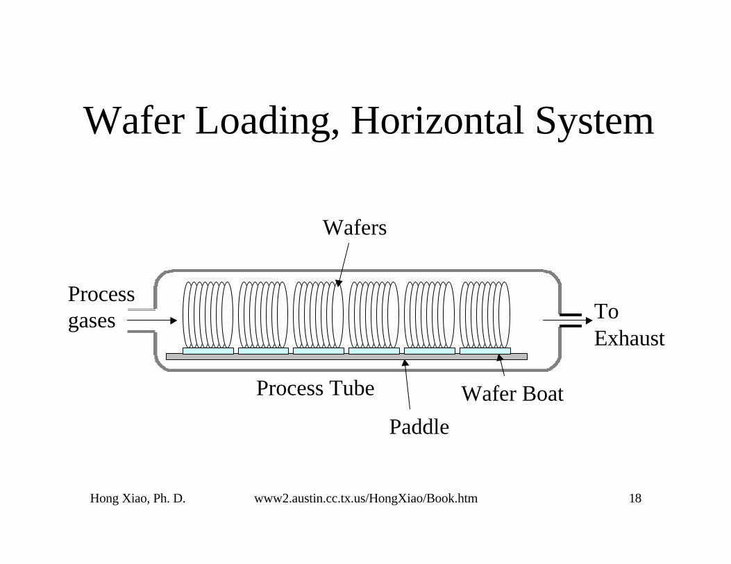
Wafer Loading, Horizontal System
ToExhaust
Process Tube Wafer Boat
Paddle
Processgases
Wafers

Hong Xiao, Ph. D. www2.austin.cc.tx.us/HongXiao/Book.htm 19
Wafer Loading, Vertical System
Wafers
TowerSuscepter

Hong Xiao, Ph. D. www2.austin.cc.tx.us/HongXiao/Book.htm 20
• Thermal processes are very sensitive to thetemperature
• Precisely temperature control is vital
• ±0.5 °C at central zone
• ±0.05% at 1000 °C!
Temperature Control

Hong Xiao, Ph. D. www2.austin.cc.tx.us/HongXiao/Book.htm 21
Temperature Control System
• Thermocouples touching the reaction tube
• Proportional band controllers feed the powerto the heating coils
• The heating power is proportional todifference between setting point andmeasured value

Hong Xiao, Ph. D. www2.austin.cc.tx.us/HongXiao/Book.htm 22
Reaction Chamber
• High-purity Quartz– Stability at high temperature
– Basic Cleanliness
• Drawback– Fragility
– Some metallic ions
– Not a sodium barrier
– Small flakes at > 1200 °C, devitrification

Hong Xiao, Ph. D. www2.austin.cc.tx.us/HongXiao/Book.htm 23
Horizontal Furnace
Center Zone
Flat Zone
Distance
Temperature
Heating Coils
QuartzTube
Gas flow
Wafers

Hong Xiao, Ph. D. www2.austin.cc.tx.us/HongXiao/Book.htm 24
Vertical Furnace, Process Position
ProcessChamber
Wafers
Tower
Heaters
Suscepter

Hong Xiao, Ph. D. www2.austin.cc.tx.us/HongXiao/Book.htm 25
Quartz Tube
• Electric Fused
• Flame Fused
• Both of them as trace amount of metals
• Flame-fused tubes produced devices havebetter characteristics.

Hong Xiao, Ph. D. www2.austin.cc.tx.us/HongXiao/Book.htm 26
Quartz Tube Clean
• Very important especially for depositionfurnace to prevent particle contamination
• Out side fab, ex-situ– Hydrofluoric acid (HF) tank
– Remove a thin layer of quartz every time
– limited tube lifetime
• In-situ clean– Plasma generator inside tube
– Free fluorine from NF3 etch away contaminant

Hong Xiao, Ph. D. www2.austin.cc.tx.us/HongXiao/Book.htm 27
Silicon Carbide Tube
• Pro– Higher thermal stability
– Better metallic ion barrier
• Con– Heavier
– More expensive

Hong Xiao, Ph. D. www2.austin.cc.tx.us/HongXiao/Book.htm 28
Temperature ControlAnti-Warp Methods
• Ramping– Load wafer slowly at a lower temperature (idle
temperature, ~ 800 °C)
– Ramp temperature to process point after a shortstabilization period
• Slow loading– 1 inch/min
– thermal capacity of 200 six-inch wafers candrop temperature as much as 50 °C

Hong Xiao, Ph. D. www2.austin.cc.tx.us/HongXiao/Book.htm 29
Horizontal Furnace
• Contain 3 or 4 tubes (reaction chambers)
• Separate temperature control system foreach tube

Hong Xiao, Ph. D. www2.austin.cc.tx.us/HongXiao/Book.htm 30
Horizontal Furnace
Center Zone
Flat Zone
Distance
Temperature
Heating Coils
QuartzTube
Gas flow
Wafers

Hong Xiao, Ph. D. www2.austin.cc.tx.us/HongXiao/Book.htm 31
Furnace
• Wafer Clean Station
• Wafer Loading Station– Manual wafer loading
– Automatic wafer loading
• Oxidation Process Automation

Hong Xiao, Ph. D. www2.austin.cc.tx.us/HongXiao/Book.htm 32
Vertical Furnaces
• Smaller footprint
• Better contamination control
• Better wafer handling
• Lower maintenance cost and higher uptime
• Place the process tube in vertical direction

Hong Xiao, Ph. D. www2.austin.cc.tx.us/HongXiao/Book.htm 33
Vertical Furnace, Loading andUnloading Position
ProcessChamber
Wafers
Tower
Heaters
Suscepter

Hong Xiao, Ph. D. www2.austin.cc.tx.us/HongXiao/Book.htm 34
Smaller Footprint
• Clean room footage becomes very expensive
• Small footprint reduces cost of ownership (COO)

Hong Xiao, Ph. D. www2.austin.cc.tx.us/HongXiao/Book.htm 35
Better Contamination Control
• Better uniformity for Laminar gas flow control
• Gas flow from top to bottom
• Particles has less chance to fall at the center ofthe wafers
Hong Xiao, Ph. D. www2.austin.cc.tx.us/HongXiao/Book.htm 36
Better Wafer Handling
• High torque on paddle of horizontal when ithandle large amount of large diameter wafers
• Zero torque for wafer tower in vertical system

Hong Xiao, Ph. D. www2.austin.cc.tx.us/HongXiao/Book.htm 37
Summery of Hardware
• Furnaces are commonly used in thermal processes
• Furnaces usually consist with control system, gasdelivery system, process tube or chamber, waferloading system, and exhaust system.
• Vertical furnace is more widely used due to itsmaller footprint, better contamination control,and lower maintenance.
• Precise temperature and its uniformity is vital forthe success of the thermal processes.

Hong Xiao, Ph. D. www2.austin.cc.tx.us/HongXiao/Book.htm 38
Oxidation

Hong Xiao, Ph. D. www2.austin.cc.tx.us/HongXiao/Book.htm 39
Oxidation
• Introduction
• Applications
• Mechanism
• Process
• System
• RTO

Hong Xiao, Ph. D. www2.austin.cc.tx.us/HongXiao/Book.htm 40
Introduction
• Silicon reacts with oxygen
• Stable oxide compound
• Widely used in IC manufacturing
Si + O2 → SiO2

Hong Xiao, Ph. D. www2.austin.cc.tx.us/HongXiao/Book.htm 41
Oxidation
SiliconDioxide
Silicon
O2 O2
O2 O2
O2O2
O2
O2
O2 O2
Original Silicon Surface
45%55%
O2
O2
O2
O2
O2

Hong Xiao, Ph. D. www2.austin.cc.tx.us/HongXiao/Book.htm 42
Some Facts About SiliconName Silicon
Symbol SiAtomic number 14Atomic weight 28.0855
Discoverer Jöns Jacob BerzeliusDiscovered at Sweden
Discovery date 1824Origin of name From the Latin word "silicis" meaning "flint"
Bond length in single crystal Si 2.352 ÅDensity of solid 2.33 g/cm3
Molar volume 12.06 cm3
Velocity of sound 2200 m/secHardness 6.5
Electrical resistivity 100,000 µΩ⋅cmReflectivity 28%
Melting point 1414 °CBoiling point 2900 °C
Thermal conductivity 150 W m -1 K -1
Coefficient of linear thermalexpansion
2.6×10⁻⁶ K-1
Etchants (wet) HNO 4 and HF, KOH, etc.Etchants (dry) HBr, Cl2, NF3, etc.
CVD Precursor SiH4, SiH2Cl2, SiHCl3, and SiCl4

Hong Xiao, Ph. D. www2.austin.cc.tx.us/HongXiao/Book.htm 43
Fact About OxygenName Oxygen
Symbol OAtomic number 8Atomic weight 15.9994
Discoverer Joseph Priestley, Carl ScheeleDiscovered at England, SwedenDiscovery date 1774Origin of name From the Greek words "oxy genes" meaning
"acid" (sharp) and "forming" (acid former)Molar volume 17.36 cm3
Velocity of sound 317.5 m/secRefractivity 1.000271
Melting point 54.8 K = -218.35 °CBoiling point 90.2 K = -182.95 °C
Thermal conductivity 0.02658 W m-1 K-1
Applications Thermal oxidation, oxide CVD, reactivesputtering and photoresist stripping
Main sources O2, H2O, N2O, O3

Hong Xiao, Ph. D. www2.austin.cc.tx.us/HongXiao/Book.htm 44
Application of Oxidation
• Diffusion Masking Layer
• Surface Passivation– Screen oxide, pad oxide, barrier oxide
• Isolation– Field oxide and LOCOS
• Gate oxide

Hong Xiao, Ph. D. www2.austin.cc.tx.us/HongXiao/Book.htm 45
Diffusion Barrier
• Much lower B and P diffusion rates in SiO2
than that in Si
• SiO2 can be used as diffusion mask
Si
Dopant
SiO2 SiO2

Hong Xiao, Ph. D. www2.austin.cc.tx.us/HongXiao/Book.htm 46
Application, Surface Passivation
Si
SiO2
Pad Oxide Screen Oxide
Sacrificial Oxide Barrier Oxide
Normally thin oxide layer (~150Å) to protectsilicon defects from contamination and over-stress.

Hong Xiao, Ph. D. www2.austin.cc.tx.us/HongXiao/Book.htm 47
Screen Oxide
Photoresist Photoresist
Si Substrate
Dopant Ions
Screen Oxide

Hong Xiao, Ph. D. www2.austin.cc.tx.us/HongXiao/Book.htm 48
USG
Pad and Barrier Oxides in STI Process
SiliconPad Oxide
Nitride
SiliconPad Oxide
Nitride
Silicon
USGBarrier Oxide
Trench Etch
Trench Fill
USG CMP; USG Anneal; Nitride and Pad Oxide Strip

Hong Xiao, Ph. D. www2.austin.cc.tx.us/HongXiao/Book.htm 49
Application, Pad Oxide
Silicon nitride
Silicon Substrate
Pad Oxide
• Relieve strong tensile stress of the nitride
• Prevent stress induced silicon defects

Hong Xiao, Ph. D. www2.austin.cc.tx.us/HongXiao/Book.htm 50
Application, Device Isolation
• Electronic isolation of neighboring devices
• Blanket field oxide
• Local oxidation of silicon (LOCOS)
• Thick oxide, usually 3,000 to 10,000 Å

Hong Xiao, Ph. D. www2.austin.cc.tx.us/HongXiao/Book.htm 51
Silicon
Silicon
Silicon
Silicon Dioxide
Field Oxide
Wafer Clean
Field Oxidation
Oxide Etch
Activation Area
Blanket Field Oxide Isolation

Hong Xiao, Ph. D. www2.austin.cc.tx.us/HongXiao/Book.htm 52
LOCOS Process
Silicon nitride
P-type substrate
P-type substrate
Silicon nitride
p+p+ p+Isolation Doping
P-type substrate p+p+ p+Isolation Doping
SiO2
Pad Oxide
Pad oxidation, nitride deposition and patterning
LOCOS oxidation
Nitride and pad oxide strip
Bird’s Beak
SiO2

Hong Xiao, Ph. D. www2.austin.cc.tx.us/HongXiao/Book.htm 53
LOCOS
• Compare with blanket field oxide– Better isolation
– Lower step height
– Less steep sidewall
• Disadvantage– rough surface topography
– Bird’s beak
• Replacing by shallow trench isolation (STI)

Hong Xiao, Ph. D. www2.austin.cc.tx.us/HongXiao/Book.htm 54
Application, Sacrificial Oxide
N-WellP-WellSTI USG
N-WellP-WellSTI USG
N-WellP-WellSTI USG
Sacrificial Oxidation
Strip Sacrificial Oxide
Gate Oxidation
Sacrificial Oxide
Gate Oxide
• Defects removal from silicon surface

Hong Xiao, Ph. D. www2.austin.cc.tx.us/HongXiao/Book.htm 55
Application, Device Dielectric• Gate oxide: thinnest and most critical layer
• Capacitor dielectric
Poly Si
Si Substrate
n+
Gate
Thin oxide
Source Drainp-Si
n+
VD > 0
Electrons
VG

Hong Xiao, Ph. D. www2.austin.cc.tx.us/HongXiao/Book.htm 56
Oxide and Applications
Name of the Oxide Thickness Application Time in application
Native 15 - 20 Å undesirable -
Screen ~ 200 Å Implantation Mid-70s to present
Masking ~ 5000 Å Diffusion 1960s to mid-1970s
Field and LOCOS 3000 - 5000 Å Isolation 1960s to 1990s
Pad 100 - 200 Å Nitride stress buffer 1960s to present
Sacrificial <1000 Å Defect removal 1970s to present
Gate 30 - 120 Å Gate dielectric 1960s to present
Barrier 100 - 200 Å STI 1980s to present
Hong Xiao, Ph. D. www2.austin.cc.tx.us/HongXiao/Book.htm 57
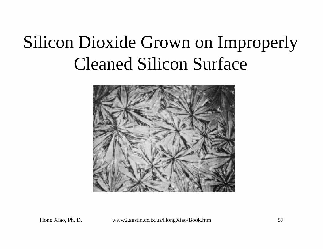
Silicon Dioxide Grown on ImproperlyCleaned Silicon Surface

Hong Xiao, Ph. D. www2.austin.cc.tx.us/HongXiao/Book.htm 58
Pre-oxidation Wafer Clean
• Particulates
• Organic residues
• Inorganic residues
• Native oxide layers

Hong Xiao, Ph. D. www2.austin.cc.tx.us/HongXiao/Book.htm 59
RCA Clean
• Developed by Kern and Puotinen in 1960 at RCA
• Most commonly used clean processes in IC fabs
• SC-1-- NH4OH:H2O2:H2O with 1:1:5 to 1:2:7 ratioat 70 to 80 °C to remove organic contaminants.
• SC-2-- HCl:H2O2:H2Owith 1:1:6 to 1:2:8 ratio at70 to 80 °C to remove inorganic contaminates.
• DI water rinse
• HF dip or HF vapor etch to remove native oxide.

Hong Xiao, Ph. D. www2.austin.cc.tx.us/HongXiao/Book.htm 60
• High purity deionized (DI) water orH2SO4:H2O2 followed by DI H2O rinse.
• High pressure scrub or immersion in heateddunk tank followed by rinse, spin dry and/ordry bake (100 to 125 °C).
Pre-oxidation Wafer CleanParticulate Removal

Hong Xiao, Ph. D. www2.austin.cc.tx.us/HongXiao/Book.htm 61
• Strong oxidants remove organic residues.
• H2SO4:H2O2 or NH3OH:H2O2 followed byDI H2O rinse.
• High pressure scrub or immersion in heateddunk tank followed by rinse, spin dry and/ordry bake (100 to 125 °C).
Pre-oxidation Wafer CleanOrganic Removal

Hong Xiao, Ph. D. www2.austin.cc.tx.us/HongXiao/Book.htm 62
• HCl:H2O.
• Immersion in dunk tank followed by rinse,spin dry and/or dry bake (100 to 125 °C).
Pre-oxidation Wafer CleanInorganic Removal

Hong Xiao, Ph. D. www2.austin.cc.tx.us/HongXiao/Book.htm 63
• HF:H2O.
• Immersion in dunk tank or single wafervapor etcher followed by rinse, spin dryand/or dry bake (100 to 125 °C).
Pre-oxidation Wafer CleanNative Oxide Removal

Hong Xiao, Ph. D. www2.austin.cc.tx.us/HongXiao/Book.htm 64
Oxidation Mechanism
• Si + O2 SiO2
• Oxygen comes from gas
• Silicon comes from substrate
• Oxygen diffuse cross existing silicondioxide layer and react with silicon
• The thicker of the film, the lower of thegrowth rate

Hong Xiao, Ph. D. www2.austin.cc.tx.us/HongXiao/Book.htm 65
Oxide Growth Rate RegimeO
xide
Thi
ckne
ss
Oxidation Time
Linear Growth RegimeB
AX = t
Diffusion-limited Regime
X = √ B t

Hong Xiao, Ph. D. www2.austin.cc.tx.us/HongXiao/Book.htm 66
<100> Silicon Dry Oxidation
2 4 6 8 10 12 14 16 18 20
0.2
0
0.4
0.6
0.8
1.0
1.2
Oxidation Time (hours)
Oxi
de T
hick
ness
(m
icro
n)
1200 °C
1150 °C
1100 °C
1050 °C
1000 °C
950 °C
900 °C
<100> Silicon Dry Oxidation

Hong Xiao, Ph. D. www2.austin.cc.tx.us/HongXiao/Book.htm 67
Wet (Steam) Oxidation
• Si + 2H2O SiO2 + 2H2
• At high temperature H2O is dissociated to Hand H-O
• H-O diffuses faster in SiO2 than O2
• Wet oxidation has higher growth rate thandry oxidation.

Hong Xiao, Ph. D. www2.austin.cc.tx.us/HongXiao/Book.htm 68
<100> Silicon Wet Oxidation Rate
2 4 6 8 10 12 14 16 18 20
0.5
0
1.0
1.5
2.0
2.5
3.0
Oxidation Time (hours)
Oxi
de T
hick
ness
(m
icro
n)1150 °C
1100 °C
1050 °C
1000 °C
950 °C
900 °C
<100> Silicon Wet Oxidation

Hong Xiao, Ph. D. www2.austin.cc.tx.us/HongXiao/Book.htm 69
Oxidation Rate
• Temperature
• Chemistry, wet or dry oxidation
• Thickness
• Pressure
• Wafer orientation (<100> vs. <111>)
• Silicon dopant

Hong Xiao, Ph. D. www2.austin.cc.tx.us/HongXiao/Book.htm 70
• Oxidation rate is very sensitive(exponentially related) to temperature
• Higher temperature will have much higheroxidation rate.
• The higher of temperature is, the higher ofthe chemical reaction rate between oxygenand silicon is and the higher diffusion rateof oxygen in silicon dioxide is.
Oxidation RateTemperature

Hong Xiao, Ph. D. www2.austin.cc.tx.us/HongXiao/Book.htm 71
Oxidation RateWafer Orientation
• <111> surface has higher oxidation ratethan <100> surface.
• More silicon atoms on the surface.

Hong Xiao, Ph. D. www2.austin.cc.tx.us/HongXiao/Book.htm 72
Wet Oxidation Rate
1 2 3 40
Oxidation Time (hours)
0.4
0.8
1.2
1.6
0.2
0.6
1.0
1.4
1.8O
xide
Thi
ckne
ss (
mic
ron)
<111> Orientation
95 °C Water
1200 °C
1100 °C
1000 °C
920 °C

Hong Xiao, Ph. D. www2.austin.cc.tx.us/HongXiao/Book.htm 73
• Dopant elements and concentration
• Highly phosphorus doped silicon has highergrowth rate, less dense film and etch faster.
• Generally highly doped region has highergrow rate than lightly doped region.
• More pronounced in the linear stage (thinoxides) of oxidation.
Oxidation Rate Dopant Concentration

Hong Xiao, Ph. D. www2.austin.cc.tx.us/HongXiao/Book.htm 74
Oxidation: DopantsPile-up and Depletion Effects
•N-type dopants (P, As, Sb) have highersolubility in Si than in SiO2, when SiO2
grow they move into silicon, it is callpile-up or snowplow effect.
•Boron tends to go to SiO2, it is calleddepletion effect.

Hong Xiao, Ph. D. www2.austin.cc.tx.us/HongXiao/Book.htm 75
Depletion and Pile-up Effects
Si-SiO2 interface
SiO2
Dop
ant C
once
ntra
tion
Si
Si-SiO2 interface
SiO2D
opan
t Con
cent
rati
onSi
P-type Dopant Depletion N-type dopant Pile-up
Original Si Surface Original Si Surface
Original Distribution

Hong Xiao, Ph. D. www2.austin.cc.tx.us/HongXiao/Book.htm 76
Oxidation Rate Doped oxidation (HCl)
• HCl is used to reduce mobile ion contamination.
• Widely used for gate oxidation process.
• Growth rate can increase from 1 to 5 percent.

Hong Xiao, Ph. D. www2.austin.cc.tx.us/HongXiao/Book.htm 77
Oxidation Rate Differential Oxidation
• The thicker of the oxide film is, the slower ofthe oxidation rate is.
• Oxygen need more time to diffuse cross theexisting oxide layer to react with substratesilicon.

Hong Xiao, Ph. D. www2.austin.cc.tx.us/HongXiao/Book.htm 78
Pre-oxidation Clean
• Thermally grown SiO2 is amorphous.
• Tends to cross-link to form a crystal
• In nature, SiO2 exists as quartz and sand
• Defects and particles can be the nucleation sites
• Crystallized SiO2 with poor barrier capability.
• Need clean silicon surface before oxidation.

Hong Xiao, Ph. D. www2.austin.cc.tx.us/HongXiao/Book.htm 79
Oxidation Process
• Dry Oxidation, thin oxide– Gate oxide
– Pad oxide, screen oxide, sacrificial oxide, etc.
• Wet Oxidation, thick oxide– Field oxide
– Diffusion masking oxide

Hong Xiao, Ph. D. www2.austin.cc.tx.us/HongXiao/Book.htm 80
Dry Oxidation System
ToProcessTube
MFC
MFC
MFC
Control Valves
Regulator
Pro
cess
N2
Pur
ge N
2
O2
HC
l
MFC

Hong Xiao, Ph. D. www2.austin.cc.tx.us/HongXiao/Book.htm 81
Dry Oxidation
• Dry O2 as the main process gas
• HCl is used to remove mobile ions forgate oxidation
• High purity N2 as process purge gas
• Lower grade N2 as idle purge gas

Hong Xiao, Ph. D. www2.austin.cc.tx.us/HongXiao/Book.htm 82
Gate Oxidation Steps
• Idle with purge N2 flow
• Idle with process N2 flow
• Wafer boats push-in with process N2 flow
• Temperature ramp-up with process N2 flow
• Temperature stabilization with process N2 flow
• Oxidation with O2, HCl, stop N2 flow

Hong Xiao, Ph. D. www2.austin.cc.tx.us/HongXiao/Book.htm 83
Dangling Bonds and Interface Charge
SiO2
Si
+ + + + +
DanglingBond
Si-SiO2
Interface
Interface State Charge (Positive)
Hong Xiao, Ph. D. www2.austin.cc.tx.us/HongXiao/Book.htm 84
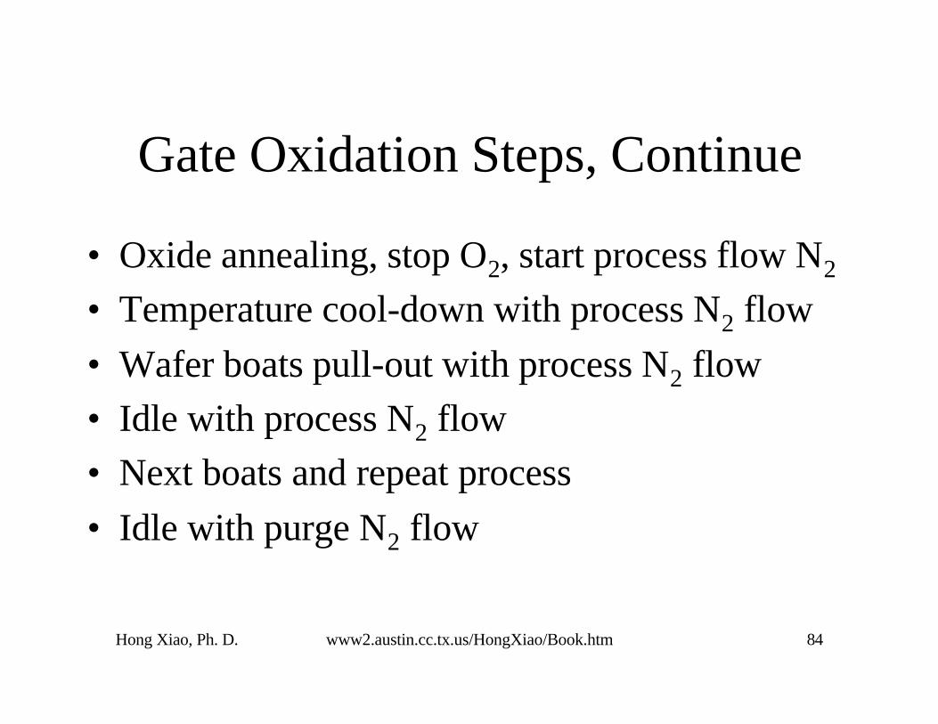
Gate Oxidation Steps, Continue
• Oxide annealing, stop O2, start process flow N2
• Temperature cool-down with process N2 flow
• Wafer boats pull-out with process N2 flow
• Idle with process N2 flow
• Next boats and repeat process
• Idle with purge N2 flow
Hong Xiao, Ph. D. www2.austin.cc.tx.us/HongXiao/Book.htm 85
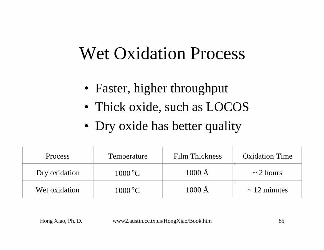
Wet Oxidation Process
• Faster, higher throughput
• Thick oxide, such as LOCOS
• Dry oxide has better quality
Process Temperature Film Thickness Oxidation Time
Dry oxidation 1000 °C 1000 Å ~ 2 hours
Wet oxidation 1000 °C 1000 Å ~ 12 minutes

Hong Xiao, Ph. D. www2.austin.cc.tx.us/HongXiao/Book.htm 86
Water Vapor Sources
• Boiler
• Bubbler
• Flush
• Pyrogenic

Hong Xiao, Ph. D. www2.austin.cc.tx.us/HongXiao/Book.htm 87
MFCProcessTube
Water
Heater
Heated Gas line Heated Fore line
Exhaust
Vapor Bubbles
Boiler System

Hong Xiao, Ph. D. www2.austin.cc.tx.us/HongXiao/Book.htm 88
Bubbler System
Heater
MFCProcessTube
Exhaust
N2
N2 Bubbles
Heated Gas Line
N2 + H2O
Water

Hong Xiao, Ph. D. www2.austin.cc.tx.us/HongXiao/Book.htm 89
Flush System
MFCProcessTube
Water
N2
Hot Plate
Heater

Hong Xiao, Ph. D. www2.austin.cc.tx.us/HongXiao/Book.htm 90
Pyrogenic Steam System
H2
O2
Thermal Couple
ToExhaust
Hydrogen Flame, 2 H2 + O2 → 2 H2O
Process Tube Wafer Boat
Paddle

Hong Xiao, Ph. D. www2.austin.cc.tx.us/HongXiao/Book.htm 91
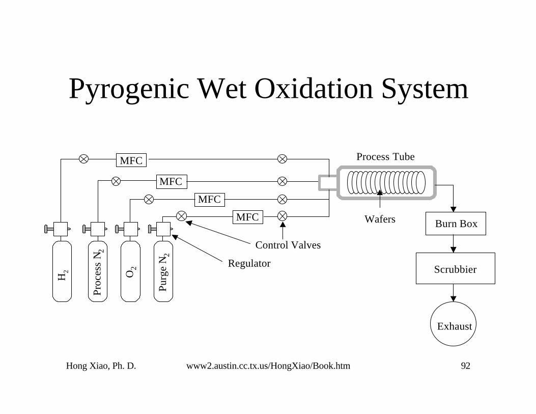
Pyrogenic System
• Advantage– All gas system
– Precisely control of flow rate
• Disadvantage– Introducing of flammable, explosive hydrogen
• Typical H2:O2 ratio is between 1.8:1 to 1.9:1.
Hong Xiao, Ph. D. www2.austin.cc.tx.us/HongXiao/Book.htm 92
Pyrogenic Wet Oxidation System
MFC
MFC
MFC
Control Valves
Regulator
Pro
cess
N2
Pur
ge N
2
O2
H2
MFC
Scrubbier
Exhaust
Process Tube
Wafers Burn Box

Hong Xiao, Ph. D. www2.austin.cc.tx.us/HongXiao/Book.htm 93
Wet Oxidation Process Steps
• Idle with purge N2 flow
• Idle with process N2 flow
• Ramp O2 with process N2 flow
• Wafer boat push-in with process N2 and O2 flows
• Temperature ramp-up with process N2 and O2 flows
• Temperature stabilization with process N2 and O2 flows
• Ramp O2, turn-off N2 flow
• Stabilize the O2 flow
Hong Xiao, Ph. D. www2.austin.cc.tx.us/HongXiao/Book.htm 94
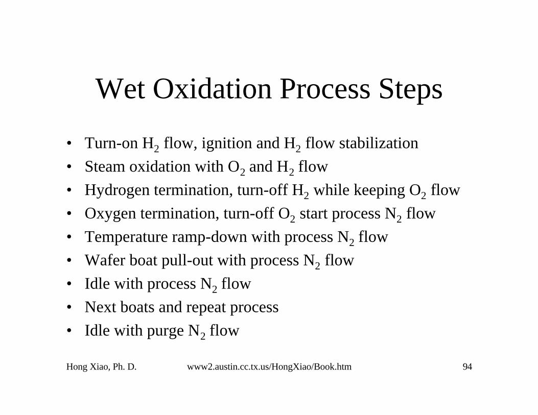
Wet Oxidation Process Steps
• Turn-on H2 flow, ignition and H2 flow stabilization
• Steam oxidation with O2 and H2 flow
• Hydrogen termination, turn-off H2 while keeping O2 flow
• Oxygen termination, turn-off O2 start process N2 flow
• Temperature ramp-down with process N2 flow
• Wafer boat pull-out with process N2 flow
• Idle with process N2 flow
• Next boats and repeat process
• Idle with purge N2 flow

Hong Xiao, Ph. D. www2.austin.cc.tx.us/HongXiao/Book.htm 95
Rapid Thermal Oxidation
• For gate oxidation of deep sub-micron device
• Very thin oxide film, < 30 Å
• Need very good control of temperatureuniformity, WIW and WTW.
• RTO will be used to achieve the devicerequirement.

Hong Xiao, Ph. D. www2.austin.cc.tx.us/HongXiao/Book.htm 96
RTP Process Diagram
Time
Rampup 1& 2
Cooldown
RTALoadwafer
Unloadwafer
RTO
O2 flow
N2 flow
HCl flow
Temperature

Hong Xiao, Ph. D. www2.austin.cc.tx.us/HongXiao/Book.htm 97
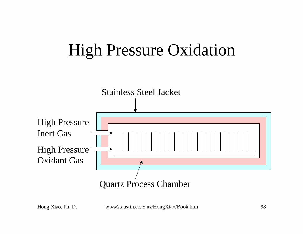
High Pressure Oxidation
• Faster growth rate
• Reducing oxidation temperature:– 1 amt. = –30 °C
• Higher dielectric strength
Hong Xiao, Ph. D. www2.austin.cc.tx.us/HongXiao/Book.htm 98
High Pressure Oxidation
High PressureInert Gas
High PressureOxidant Gas
Stainless Steel Jacket
Quartz Process Chamber

Hong Xiao, Ph. D. www2.austin.cc.tx.us/HongXiao/Book.htm 99
High Pressure Oxidation
Temperature Pressure Time
1 atmosphere 5 hours
1000 °C 5 atmosphere 1 hour
25 atmosphere 12 minutes
Oxidation time to grow 10,000 Å wet oxide

Hong Xiao, Ph. D. www2.austin.cc.tx.us/HongXiao/Book.htm 100
High Pressure Oxidation
Time Pressure Temperature
1 atmosphere 1000 °C
5 hours 10 atmosphere 700 °C
Oxidation temperature to grow 10,000 Å wet oxide in 5 hours

Hong Xiao, Ph. D. www2.austin.cc.tx.us/HongXiao/Book.htm 101
High Pressure Oxidation
• Complex system
• Safety issues
• Not widely used in IC production

Hong Xiao, Ph. D. www2.austin.cc.tx.us/HongXiao/Book.htm 102
Oxide Measurement
• Thickness
• Uniformity
• Color chart
• Ellipsometry
• Reflectometry
• Gate oxide
• Break downvoltage
• C-Vcharacteristics

Hong Xiao, Ph. D. www2.austin.cc.tx.us/HongXiao/Book.htm 103
Linearly Polarized Incident Light
Elliptically PolarizedReflected Light
n1, k1, t1
n2, k2
sp
Ellipsometry

Hong Xiao, Ph. D. www2.austin.cc.tx.us/HongXiao/Book.htm 104
t
21
Substrate
Dielectric film, n(λ)
Incident light
Human eye orphotodetector
Reflectometry

Hong Xiao, Ph. D. www2.austin.cc.tx.us/HongXiao/Book.htm 105
C-V Test Configuration
CapacitorMeter
Aluminum
Metal Platform
Silicon
Oxide
Large Resistor
HeaterHeater

Hong Xiao, Ph. D. www2.austin.cc.tx.us/HongXiao/Book.htm 106
Summary of Oxidation
• Oxidation of silicon
• High stability and relatively easy to get.
• Application– Isolation, masking, pad, barrier, gate, and etc.
• Wet and Dry
• More dry processes for advanced IC chips
• Rapid thermal oxidation and annealing forultra-thin gate oxide
Hong Xiao, Ph. D. www2.austin.cc.tx.us/HongXiao/Book.htm 107
Diffusion

Hong Xiao, Ph. D. www2.austin.cc.tx.us/HongXiao/Book.htm 108
Diffusion
• Most common physics phenomena
• Materials disperse from higher concentrationto lower concentration region
• Silicon dioxide as diffusion mask
• Was widely used for semiconductor doping
• “Diffusion Furnace” and “Diffusion Bay”

Hong Xiao, Ph. D. www2.austin.cc.tx.us/HongXiao/Book.htm 109
Illustration of Diffusion Doping
Dopant
Silicon

Hong Xiao, Ph. D. www2.austin.cc.tx.us/HongXiao/Book.htm 110
Illustration of Diffusion Doping
Dopant
Silicon
Junction Depth

Hong Xiao, Ph. D. www2.austin.cc.tx.us/HongXiao/Book.htm 111
Definition of Junction depth
Background dopant concentration
Junction Depth, xj
Distance from the wafer surface
Dopant Concentration

Hong Xiao, Ph. D. www2.austin.cc.tx.us/HongXiao/Book.htm 112
Diffusion
N-Silicon
Masking Oxide
N-Siliconp+ p+
Masking Oxide

Hong Xiao, Ph. D. www2.austin.cc.tx.us/HongXiao/Book.htm 113
Diffusion
• Replaced by ion implantation due to the lessprocess control
• Still being used in drive-in for well formation
Hong Xiao, Ph. D. www2.austin.cc.tx.us/HongXiao/Book.htm 114
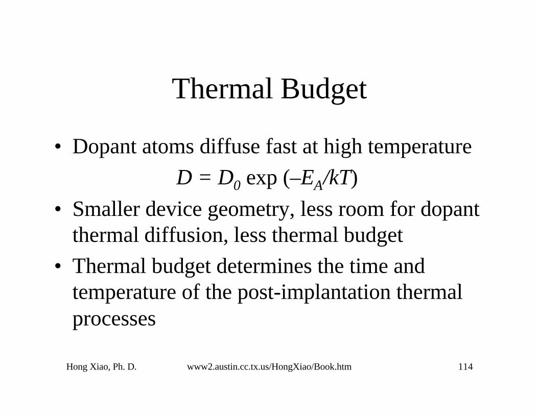
Thermal Budget
• Dopant atoms diffuse fast at high temperature
D = D0 exp (–EA/kT)
• Smaller device geometry, less room for dopantthermal diffusion, less thermal budget
• Thermal budget determines the time andtemperature of the post-implantation thermalprocesses

Hong Xiao, Ph. D. www2.austin.cc.tx.us/HongXiao/Book.htm 115
Illustration of Thermal Budget
As S/D Implantation Over Thermal Budget
Gate

Hong Xiao, Ph. D. www2.austin.cc.tx.us/HongXiao/Book.htm 116
1 µm
Thermal Budget
1
10
100
1000
104/T (K)7 8 9 10
10001100 900 800
2 µm
0.5 µm
0.25 µm
The
rmal
Bud
get (
sec)
T (°C)
Source: Changand Sze, ULSITechnology

Hong Xiao, Ph. D. www2.austin.cc.tx.us/HongXiao/Book.htm 117
Diffusion Doping Process
• Both dopant concentration and junction depthare related to temperature.
• No way to independently to control both factor
• Isotropic dopant profile
• Replaced by ion implantation after the mid-1970s.

Hong Xiao, Ph. D. www2.austin.cc.tx.us/HongXiao/Book.htm 118
Diffusion Doping Process
• Silicon dioxide as hard mask
• Deposit dopant oxide
• Cap oxidation– prevent dopant diffusion into gas phase
• Drive-in

Hong Xiao, Ph. D. www2.austin.cc.tx.us/HongXiao/Book.htm 119
Diffusion Doping Process• Oxidation, photolithography and oxide etch• Pre-deposition:
B2H6 + 2 O2 → B2O3 + 3 H2O• Cap oxidation:
2 B2O3 + 3 Si → 3 SiO2 + 4 B2 H2O + Si → SiO2 + 2 H2
• Drive-in– Boron diffuses into silicon substrate

Hong Xiao, Ph. D. www2.austin.cc.tx.us/HongXiao/Book.htm 120
Diffusion Doping Process
• Oxidation, photolithography and oxide etch
• Deposit dopant oxide:
4POCl3 + 3O2 → 2P2O5 + 3Cl2
• Cap oxidation
2P2O5 + 5Si → 5SiO2 + 4P– Phosphorus concentrates on silicon surface
• Drive-in– Phosphorus diffuses into silicon substrate

Hong Xiao, Ph. D. www2.austin.cc.tx.us/HongXiao/Book.htm 121
Phosphorus Diffusion System
MFC
MFC
MFC
Control Valves
Regulator
Proc
ess
N2
Purg
e N
2
O2
POC
l 3
MFC
Scrubbier
Exhaust
Process Tube
Wafers Burn Box

Hong Xiao, Ph. D. www2.austin.cc.tx.us/HongXiao/Book.htm 122
Si Substrate
Wafer Clean

Hong Xiao, Ph. D. www2.austin.cc.tx.us/HongXiao/Book.htm 123
Si Substrate
Oxidation
SiO2

Hong Xiao, Ph. D. www2.austin.cc.tx.us/HongXiao/Book.htm 124
Si Substrate
Doped Area Patterning
SiO2
PR
Hong Xiao, Ph. D. www2.austin.cc.tx.us/HongXiao/Book.htm 125
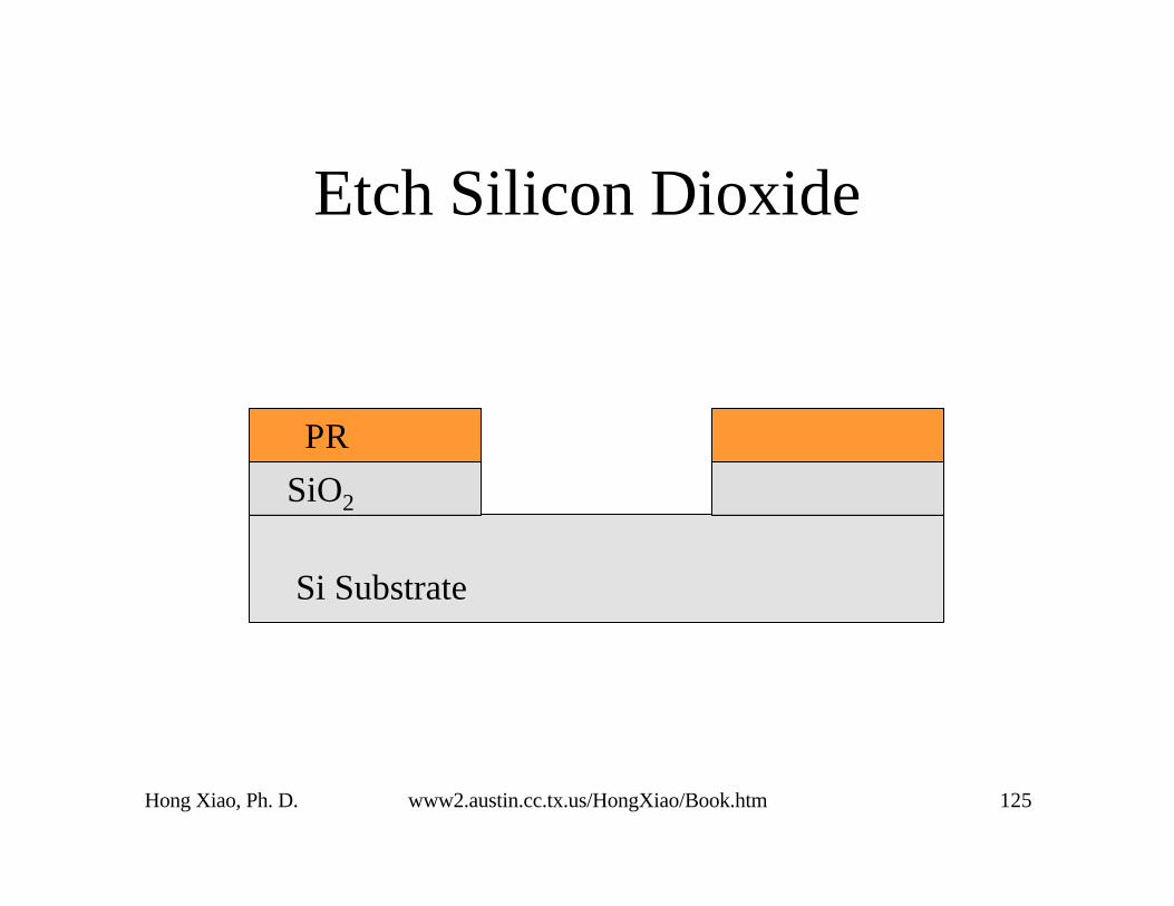
Si Substrate
Etch Silicon Dioxide
SiO2
PR

Hong Xiao, Ph. D. www2.austin.cc.tx.us/HongXiao/Book.htm 126
Si Substrate
Strip Photoresist
SiO2

Hong Xiao, Ph. D. www2.austin.cc.tx.us/HongXiao/Book.htm 127
Si Substrate
Wafer Clean
SiO2

Hong Xiao, Ph. D. www2.austin.cc.tx.us/HongXiao/Book.htm 128
Si Substrate
Dopant Oxide Deposition
SiO2
Deposited Dopant Oxide

Hong Xiao, Ph. D. www2.austin.cc.tx.us/HongXiao/Book.htm 129
Si Substrate
Cap Oxidation
SiO2

Hong Xiao, Ph. D. www2.austin.cc.tx.us/HongXiao/Book.htm 130
Phosphoric Oxide Deposition andCap Oxidation
N2 Flow
POCl3 Flow
O2 Flow
Push PullTempRamp
Temp.Stab.
Dopant Deposition CapOxide
RampDown
WaferPosition
Temperature
N2
Vent

Hong Xiao, Ph. D. www2.austin.cc.tx.us/HongXiao/Book.htm 131
Drive-in
Si Substrate
SiO2

Hong Xiao, Ph. D. www2.austin.cc.tx.us/HongXiao/Book.htm 132
Si Substrate
Strip Oxide, Ready for Next Step
SiO2

Hong Xiao, Ph. D. www2.austin.cc.tx.us/HongXiao/Book.htm 133
Phosphorus Drive-in
Temperature
N2 Flow
O2 Flow
Push TempRamp
Temp.Stab.
Drive-in
WaferPosition
PullRampDown
Stab.

Hong Xiao, Ph. D. www2.austin.cc.tx.us/HongXiao/Book.htm 134
Limitations and Applications
• Diffusion is isotropic process and alwaysdope underneath masking oxide
• Can’t independently control junction depthand dopant concentration
• Used for well implantation drive-in
• R&D for ultra shallow junction (USJ)formation

Hong Xiao, Ph. D. www2.austin.cc.tx.us/HongXiao/Book.htm 135
Application of Diffusion: Drive-in
• Wells have the deepest junction depth
• Need very high ion implantation energy
• Cost of MeV ion implanters is very high
• Diffusion can help to drive dopant to thedesired junction depth while annealing

Hong Xiao, Ph. D. www2.austin.cc.tx.us/HongXiao/Book.htm 136
Well Implantation and Drive-in
P-Epi
Photoresist
N-Well
P+
P-Epi N-Well

Hong Xiao, Ph. D. www2.austin.cc.tx.us/HongXiao/Book.htm 137
Diffusion for Boron USJ Formation
• Small devices needs ultra shallow junction
• Boron is small and light, implanter energycould be too high for it goes too deep
• Controlled thermal diffusion is used inR&D for shallow junction formation

Hong Xiao, Ph. D. www2.austin.cc.tx.us/HongXiao/Book.htm 138
Surface Clean
Si SubstrateSTI STI
Silicide
Sidewall Spacer Sidewall Spacer

Hong Xiao, Ph. D. www2.austin.cc.tx.us/HongXiao/Book.htm 139
BSG CVD
Si SubstrateSTI STI
Boro-Silicate Glass
Silicide
Sidewall Spacer Sidewall Spacer

Hong Xiao, Ph. D. www2.austin.cc.tx.us/HongXiao/Book.htm 140
RTP Dopant Drive-in
Si SubstrateSTI
Boro-Silicate Glass
STI
SilicidePolysilicon
Gate Oxide

Hong Xiao, Ph. D. www2.austin.cc.tx.us/HongXiao/Book.htm 141
Strip BSG
Si SubstrateSTISTI
SilicidePolysiliconGate Oxide

Hong Xiao, Ph. D. www2.austin.cc.tx.us/HongXiao/Book.htm 142
Doping Measurement
• Four-point probe
Rs = ρ/t

Hong Xiao, Ph. D. www2.austin.cc.tx.us/HongXiao/Book.htm 143
Four-Point Probe MeasurementFour-Point Probe Measurement
S1 S2 S3
P1 P2 P3 P4
V
I
Substrate
Doped Region

Hong Xiao, Ph. D. www2.austin.cc.tx.us/HongXiao/Book.htm 144
Summary of Diffusion
• Physics of diffusion is well understood
• Diffusion was widely used in dopingprocesses in early IC manufacturing
• Replaced by ion implantation since the mid-1970s

Hong Xiao, Ph. D. www2.austin.cc.tx.us/HongXiao/Book.htm 145
Annealing and RTP Processes

Hong Xiao, Ph. D. www2.austin.cc.tx.us/HongXiao/Book.htm 146
Post-implantation Annealing
• Energetic ions damage crystal structure
• Amorphous silicon has high resistivity
• Need external energy such as heat for atomsto recover single crystal structure
• Only in single crystal structure dopants canbe activated

Hong Xiao, Ph. D. www2.austin.cc.tx.us/HongXiao/Book.htm 147
Post-implantation Annealing
• Single crystal structure has lowest potentialenergy
• Atoms tend to stop on lattice grid
• Heat can provide energy to atoms for fastthermal motion
• Atoms will find and settle at the lattice gridwhere has the lowest potential energy position
• Higher temperature, faster annealing

Hong Xiao, Ph. D. www2.austin.cc.tx.us/HongXiao/Book.htm 148
Before Ion Implantation
Lattice Atoms
Hong Xiao, Ph. D. www2.austin.cc.tx.us/HongXiao/Book.htm 149
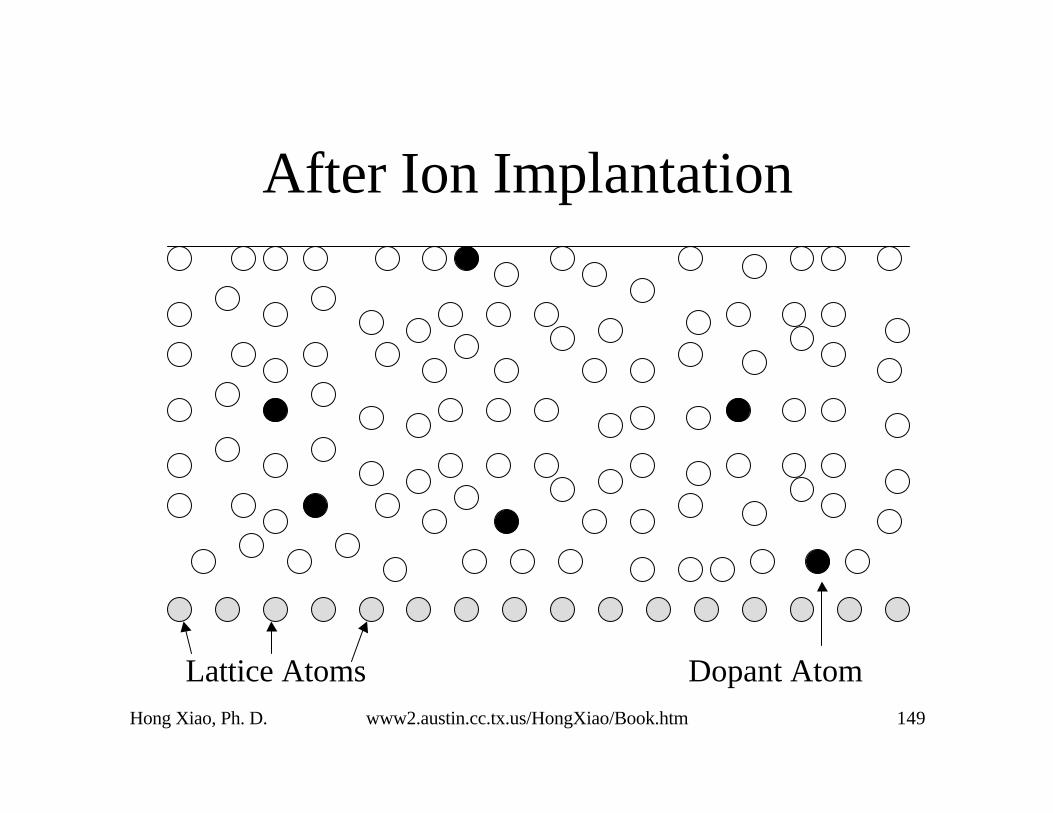
After Ion Implantation
Dopant AtomLattice Atoms

Hong Xiao, Ph. D. www2.austin.cc.tx.us/HongXiao/Book.htm 150
Thermal Annealing
Dopant AtomLattice Atoms

Hong Xiao, Ph. D. www2.austin.cc.tx.us/HongXiao/Book.htm 151
Thermal Annealing
Dopant AtomsLattice Atoms

Hong Xiao, Ph. D. www2.austin.cc.tx.us/HongXiao/Book.htm 152
Annoy Annealing• A thermal process in which different atoms
chemically bond with each other to form ametal alloy.
• Widely used in silicide formation
• Self aligned silicide (salicide)– Titanium silicide, TiSi2
– Cobalt silicide, CoSi2
• Furnace and RTP

Hong Xiao, Ph. D. www2.austin.cc.tx.us/HongXiao/Book.htm 153
Silicide
• Much lower resistivity than polysilicon
• Used as gate and local interconnection
• Used as capacitor electrodes
• Improving device speed and reduce heatgeneration
• TiSi2, WSi2 are the most commonly usedsilicide
• CoSi2, MoSi2, and etc are also used

Hong Xiao, Ph. D. www2.austin.cc.tx.us/HongXiao/Book.htm 154
Titanium Silicide Process
• Argon sputtering clean
• Titanium PVD
• RTP Anneal, ~700 °C
• Strip titanium, H2O2:H2SO2

Hong Xiao, Ph. D. www2.austin.cc.tx.us/HongXiao/Book.htm 155
Titanium Silicide ProcessTitanium
n+n+STI p+ p+
USG
Polysilicon
n+n+ USGUSGSTI
Titanium Silicide
n+n+ USG p+ p+USGSTI
Titanium SilicideSidewall Spacer
Ti Deposition
Annealing
Ti Strip
p+ p+

Hong Xiao, Ph. D. www2.austin.cc.tx.us/HongXiao/Book.htm 156
Aluminum-silicon Alloy
• Form on silicon surface
• Prevent junction spiking due to silicondissolving in aluminum

Hong Xiao, Ph. D. www2.austin.cc.tx.us/HongXiao/Book.htm 157
p+p+
Junction Spike
n-type Silicon
AlAl AlSiO2

Hong Xiao, Ph. D. www2.austin.cc.tx.us/HongXiao/Book.htm 158
Reflow
• Flowed surface is smoother and flatter
• Easier for photolithography and metallization
• Higher temperature, better flow result
• Reflow time and temperature are determined bythe thermal budget
• Higher dopant concentration requires lowerflow temperature

Hong Xiao, Ph. D. www2.austin.cc.tx.us/HongXiao/Book.htm 159
Illustration of BPSG Reflow
P-type substrate
p+p+
N-well
SiO2n+n+ p+ p+LOCOS
PSG
P-type substrate
p+p+N-well
SiO2n+n+ p+ p+LOCOS
PSGAsDeposit
AfterReflow

Hong Xiao, Ph. D. www2.austin.cc.tx.us/HongXiao/Book.htm 160
Reflow
• Undoped silicate glass (USG) becomes softenat very high temperature T > 1500 °C, will flowdue to the surface tension
• PSG and BPSG become soften at significantlower temperature (< 1100 °C down to 850 °C)
• Phosphorus also can trap sodium
• PSG and BPSG is commonly used as pre-metaldielectric (PMD)

Hong Xiao, Ph. D. www2.austin.cc.tx.us/HongXiao/Book.htm 161
Reflow Process
• Wafer loading
• Temperature rump-up
• Temperature stabilization
• Reflow
• Temperature rump-down
• Wafer unloading

Hong Xiao, Ph. D. www2.austin.cc.tx.us/HongXiao/Book.htm 162
Reflow Process
• Reflow usually used N2 ambient
• Sometimes H2O vapor is also used
• H2O helps to filly oxidize dopant atoms

Hong Xiao, Ph. D. www2.austin.cc.tx.us/HongXiao/Book.htm 163
Reflow Process
• Smaller device, less thermal budget
• No enough thermal budget for reflowfor sub-0.25 µm devices
• PSG anneal (~750 °C) instead of reflow

Hong Xiao, Ph. D. www2.austin.cc.tx.us/HongXiao/Book.htm 164
Summary of Anneal
• The most commonly used anneal processes arepost-implantation annealing, alloy annealing andreflow
• Thermal anneal is required after ion implantationfor recover crystal structure and activationdopant atoms
• Thermal anneal helps metal to react with siliconto form silicides

Hong Xiao, Ph. D. www2.austin.cc.tx.us/HongXiao/Book.htm 165
Summary of Anneal
• Metal anneal helps to form larger grain size andreduces the resistivity
• PSG or BPSG reflow smoothens and flattens thedielectric surface and helps photolithographyand metallization processes
• RTP becomes more commonly used in annealingprocesses

Hong Xiao, Ph. D. www2.austin.cc.tx.us/HongXiao/Book.htm 166
Summary of Anneal
• Advantages of RTP– Much faster ramp rate (75 to 150 °C/sec)
– Higher temperature (up to 1200 °C)
– Faster process
– Minimize the dopant diffusion
– Better control of thermal budget
– Better wafer to wafer uniformity control

Hong Xiao, Ph. D. www2.austin.cc.tx.us/HongXiao/Book.htm 167
High TemperatureDeposition Processes

Hong Xiao, Ph. D. www2.austin.cc.tx.us/HongXiao/Book.htm 168
What is CVD
• Gas(es) or vapor(s) chemically react onsubstrate surface and form solid byproduct onthe surface as deposited thin film.
Chemical Vapor Deposition
• Other byproducts are gases and leave thesurface.
• Widely used in IC processing for metal,dielectric and silicon thin film deposition.
Hong Xiao, Ph. D. www2.austin.cc.tx.us/HongXiao/Book.htm 169
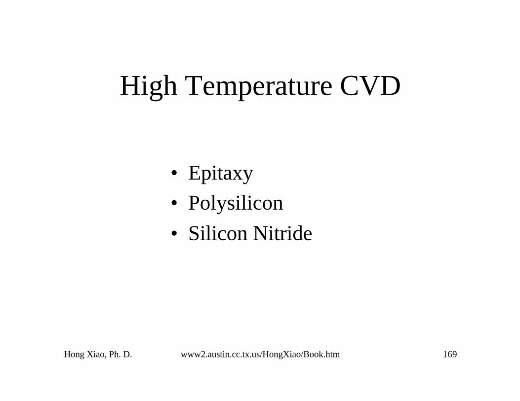
High Temperature CVD
• Epitaxy
• Polysilicon
• Silicon Nitride

Hong Xiao, Ph. D. www2.austin.cc.tx.us/HongXiao/Book.htm 170
Epitaxy
• Monocrystralline layer
• Epitaxy silicon
• Epitaxy silicon-germanium
• Epitaxy GaAs

Hong Xiao, Ph. D. www2.austin.cc.tx.us/HongXiao/Book.htm 171
Epitaxy Silicon
• Provide high quality silicon substrate withouttrace amount of oxygen and carbon.
• Required for bipolar devices.
• Needed for high performance CMOS devices.

Hong Xiao, Ph. D. www2.austin.cc.tx.us/HongXiao/Book.htm 172
Epitaxy Silicon• High temperature (~1000 °C) processes.
• Silane (SiH4), DCS (SiH2Cl2) or TCS(SiHCl3) as silicon source gases.
• Hydrogen as process gas and purge gas
• Arsine (AsH3), Phosphine (PH3), andDiborane (B2H6) are used as dopant gases.

Hong Xiao, Ph. D. www2.austin.cc.tx.us/HongXiao/Book.htm 173
Epitaxy Silicon Deposition
• Silane processHeat (1000 °C)
SiH4 → Si + H2 Silane Epi-Si Hydrogen
• DCS processHeat (1150 °C)
SiH2Cl2 → Si + 2HCl Silane Epi-Si Hydrochloride

Hong Xiao, Ph. D. www2.austin.cc.tx.us/HongXiao/Book.htm 174
Epitaxy Silicon Doping
• N-type Dopant
Heat (1000 °C)
AsH3 → As + 3/2 H2 Arsine As Hydrogen
Heat (1000 °C)
PH3 → P + 3/2 H2 Arsine Phosphorus Hydrogen

Hong Xiao, Ph. D. www2.austin.cc.tx.us/HongXiao/Book.htm 175
Epitaxy Silicon Doping
• P-type Dopant
Heat (1000 °C)
B2H6 → 2 B + 3 H2 Diborane Boron Hydrogen
Hong Xiao, Ph. D. www2.austin.cc.tx.us/HongXiao/Book.htm 176
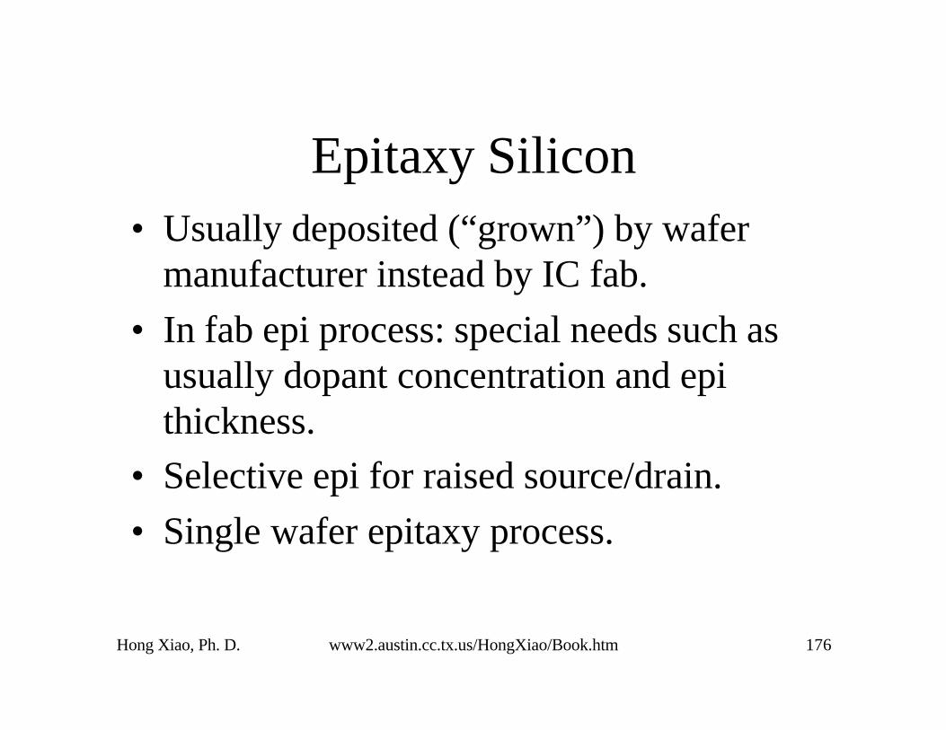
Epitaxy Silicon• Usually deposited (“grown”) by wafer
manufacturer instead by IC fab.
• In fab epi process: special needs such asusually dopant concentration and epithickness.
• Selective epi for raised source/drain.
• Single wafer epitaxy process.

Hong Xiao, Ph. D. www2.austin.cc.tx.us/HongXiao/Book.htm 177
Polysilicon
• High temperature stability.
• Reasonable good conductivity.
• Widely used for the gate and localinterconnection in MOS devices.
• Also widely used as the capacitor electrodesin memory devices, especially DRAM.

Hong Xiao, Ph. D. www2.austin.cc.tx.us/HongXiao/Book.htm 178
Polysilicon Applications in DRAM
Poly 5
Poly 4
Poly 2
Poly 3
Poly 1
TiSi2
Ta2O5 or BST
p-Siliconn+n+ n+
SidewallSpacer

Hong Xiao, Ph. D. www2.austin.cc.tx.us/HongXiao/Book.htm 179
Polysilicon
• High temperature (~700 °C) furnaceLPCVD processes.
• Silane (SiH4) or DCS (SiH2Cl2) as siliconsource gases.
• Nitrogen as purge gas
• Arsine (AsH3), Phosphine (PH3), andDiborane (B2H6) are used as dopant gases.

Hong Xiao, Ph. D. www2.austin.cc.tx.us/HongXiao/Book.htm 180
Polysilicon Deposition
• Silane processHeat (750 °C)
SiH4 → Si + H2 Silane Poly-Si Hydrogen
• DCS processHeat (750 °C)
SiH2Cl2 → Si + 2HCl Silane Poly-Si Hydrochlride

Hong Xiao, Ph. D. www2.austin.cc.tx.us/HongXiao/Book.htm 181
Polysilicon Doping
• N-type Dopant
Heat (750 °C)
AsH3 → As + 3/2 H2 Arsine As Hydrogen
Heat (750 °C)
PH3 → P + 3/2 H2Phosphine Phosphorus Hydrogen

Hong Xiao, Ph. D. www2.austin.cc.tx.us/HongXiao/Book.htm 182
Polysilicon Doping
• P-type Dopant
Heat (750 °C)
B2H6 → 2 B + 3 H2 Diborane Boron Hydrogen

Hong Xiao, Ph. D. www2.austin.cc.tx.us/HongXiao/Book.htm 183
Temperature Relationship ofSilane Process
• On single crystal silicon substrate
• Silane as source gases
• T > 900 °C deposit single crystal silicon• 900 °C > T > 550 °C deposit polysilicon• T < 550 °C deposit amorphous silicon

Hong Xiao, Ph. D. www2.austin.cc.tx.us/HongXiao/Book.htm 184
Temperature and Crystal Structurefor Silane Processes
T<550 °CAmorphous Si
T > 900 °C Single Crystal Si
550 °C <T< 900 °C Polysilicon
Grain
GrainBoundary

Hong Xiao, Ph. D. www2.austin.cc.tx.us/HongXiao/Book.htm 185
Polysilicon LPCVD System
MFC
MFC
Control Valves
Regulator
Pro
cess
N2
Pur
ge N
2
SiH
4
MFC
Scrubbier
Exhaust
Process Tube
Wafers Burn Box

Hong Xiao, Ph. D. www2.austin.cc.tx.us/HongXiao/Book.htm 186
Polysilicon Deposition Process
• Idle with purge N2 flow
• Idle with process N2 flow
• Wafer load into tower withprocess N2 flow
• Tower raises into processchamber (bell jar) with process N2
flow
• Pump down chamber to basepressure (< 2 mTorr) by turning-off N2 flow
• Stabilize wafer temperature withN2 flow and leak check
• Set up process pressure (~250 mTorr)and with N2 flow
• Turn-on SiH4 flow and turn-off N2,start deposition
• Close gate valve, fill N2 and ramp-uppressure to atmospheric pressure
• Tower lowed and wafer temperaturecooled down, with process N2 flow
• Unload wafer with process N2 flow• Idle with purge N2 flow

Hong Xiao, Ph. D. www2.austin.cc.tx.us/HongXiao/Book.htm 187
Polysilicon Deposition Process
ChamberTemperature
WaferTemperature
N2 Flow
Silane Flow
ChamberPressure
LoadWafer
UnloadWafer
RaiseTower
PumpDown
Temp.Stab.
PumpDown
Press.Stab.
Si3N4
Dep.PumpDown
N2
VentLowerTower
Wafer TowerPosition

Hong Xiao, Ph. D. www2.austin.cc.tx.us/HongXiao/Book.htm 188
Polycide Deposition System
Wafer LoadingStations
Polysilicon Deposition Chambers
WaferTransferRobot
WSixDepositionChamber
WSixDepositionChamber
CooldownChamber

Hong Xiao, Ph. D. www2.austin.cc.tx.us/HongXiao/Book.htm 189
Polycide Deposition System
Wafer LoadingStations
Poly SiDepositionChamber
Wafer TransferRobot
WSix Deposition Chamber
Cool downChamber
RTA Chamber

Hong Xiao, Ph. D. www2.austin.cc.tx.us/HongXiao/Book.htm 190
Silicon Nitride
• Dense material
• Widely used as diffusion barrier layer andpassivation layer
• LPCVD (front-end) and PECVD (back-end)
• LPCVD nitride usually is deposited in a furnace

Hong Xiao, Ph. D. www2.austin.cc.tx.us/HongXiao/Book.htm 191
Application of Silicon Nitride
• LOCOS formation as oxygen diffusion barrier
• STI formation as oxide CMP stop
• PMD barrier layer
• Etch stop layer

Hong Xiao, Ph. D. www2.austin.cc.tx.us/HongXiao/Book.htm 192
LOCOS Process
Silicon nitride
P-type substrate
P-type substrate
Silicon nitride
p+p+ p+Isolation Doping
P-type substrate p+p+ p+Isolation Doping
SiO2
Pad Oxide
Pad oxidation, nitride deposition and patterning
LOCOS oxidation
Nitride and pad oxide strip
Bird’s Beak
SiO2

Hong Xiao, Ph. D. www2.austin.cc.tx.us/HongXiao/Book.htm 193
STI Process
SiliconPad Oxide
Nitride Pad Oxidation and LPCVD Nitride
SiliconPad Oxide
Nitride
Etch Nitride and Pad Oxide
Photoresist Photoresist
SiliconPad Oxide
Nitride Strip Photoresist

Hong Xiao, Ph. D. www2.austin.cc.tx.us/HongXiao/Book.htm 194
STI Process
SiliconPad Oxide
Nitride
SiliconPad Oxide
Nitride
Silicon
USG
USGBarrier Oxide
Trench Trench on Silicon
Barrier oxidation, CVD USG Trench Fill
USG CMP; Nitride,Pad Oxide Strip

Hong Xiao, Ph. D. www2.austin.cc.tx.us/HongXiao/Book.htm 195
Self-aligned Contact Etch Stop
TiSi2
p-Silicon
SidewallSpacer
n+n+ n+
BPSGBPSG
Photoresist Photoresist
Oxide
Nitride PolyGate

Hong Xiao, Ph. D. www2.austin.cc.tx.us/HongXiao/Book.htm 196
Nitride Breakthrough
n+ n+
BPSGBPSG
Photoresist Photoresist
TiSi2
n+p-Silicon
OxideSidewallSpacer
PolyGate
Nitride

Hong Xiao, Ph. D. www2.austin.cc.tx.us/HongXiao/Book.htm 197
Strip Photoresist
n+ n+
BPSGBPSG
TiSi2
n+p-Silicon
OxideSidewallSpacer
PolyGate
Nitride

Hong Xiao, Ph. D. www2.austin.cc.tx.us/HongXiao/Book.htm 198
Deposit Ti/TiN and Tungsten
n+ n+
BPSGBPSG
TiSi2
n+p-Silicon
OxideSidewallSpacer
PolyGate
W
Ti/TiN
Nitride

Hong Xiao, Ph. D. www2.austin.cc.tx.us/HongXiao/Book.htm 199
CMP Tungsten and TiN/Ti
n+ n+
BPSGBPSG
TiSi2
n+p-Silicon
OxideSidewallSpacer
PolyGate
W
Nitride
Hong Xiao, Ph. D. www2.austin.cc.tx.us/HongXiao/Book.htm 200
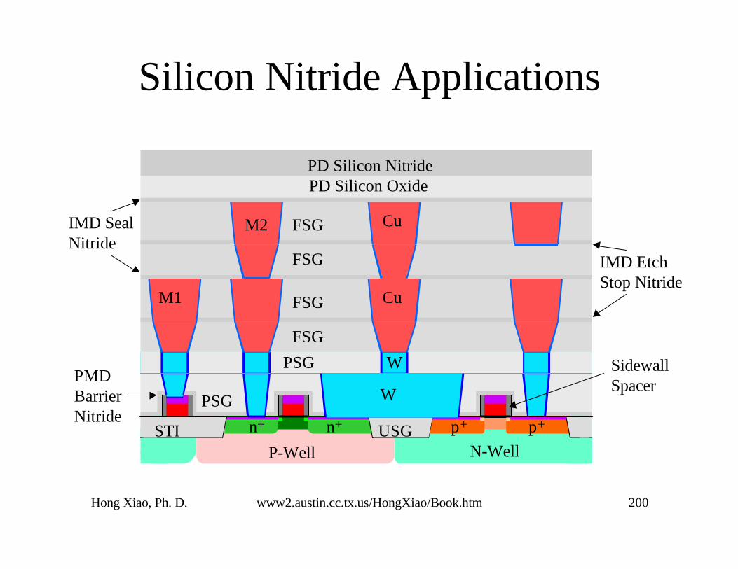
Silicon Nitride Applications
N-WellP-Well
n+STI p+ p+USG
PSG
PSG W
FSG
n+
M1 Cu
FSG
FSGM2 Cu
FSG
PD Silicon Oxide
IMD SealNitride
PMDBarrierNitride
W
PD Silicon Nitride
IMD EtchStop Nitride
SidewallSpacer

Hong Xiao, Ph. D. www2.austin.cc.tx.us/HongXiao/Book.htm 201
Silicon Nitride Deposition
• Silane or DCS as silicon source
• NH3 as nitrogen source
• N2 as purge gas
3 SiH2Cl2 + 4 NH3 → Si3N4 + 6 HCl + 6 H2
or
3 SiH4 + 4 NH3 → Si3N4 + 12 H2

Hong Xiao, Ph. D. www2.austin.cc.tx.us/HongXiao/Book.htm 202
Silicon Nitride LPCVD System
Heaters
Tower
MFC
MFC
Control Valves
RegulatorPro
cess
N2
SiH
2Cl 2
MFC
Scrubbier
Exhaust
Burn Box
Wafers
Pump
MFC
Pur
ge N
2
NH
3Process Chamber

Hong Xiao, Ph. D. www2.austin.cc.tx.us/HongXiao/Book.htm 203
Nitride Deposition Process Sequence
ChamberTemperature
WaferTemperature
N2 Flow
NH3 Flow
DCS Flow
ChamberPressure
LoadWafer
UnloadWafer
RaiseTower
PumpDown
Temp.Stab.
PumpDown
Press.Stab.
Si3N4
Dep.PumpDown
N2
VentLowerTower
Wafer TowerPosition
Hong Xiao, Ph. D. www2.austin.cc.tx.us/HongXiao/Book.htm 204
Future Trends of HT-CVD
• More single wafer rapid thermal CVD
• Integrated processes in cluster tools

Hong Xiao, Ph. D. www2.austin.cc.tx.us/HongXiao/Book.htm 205
Summary of Furnace Deposition
• Polysilicon and silicon nitride are the twomost commonly film deposited in hightemperature furnace
• Silane and DCS are the two most commonlyused silicon sources.
• Polysilicon can be doped while depositionby flowing phosphine, arsine or diborane

Hong Xiao, Ph. D. www2.austin.cc.tx.us/HongXiao/Book.htm 206
Rapid Thermal Process

Hong Xiao, Ph. D. www2.austin.cc.tx.us/HongXiao/Book.htm 207
Rapid Thermal Processing (RTP)
• Mainly used for post-implantation rapidthermal anneal (RTA) process.
• Fast temperature ramp-up, 100 to 150 °C/seccompare with 15 °C/min in horizontal furnace.
• Reduce thermal budge and easier processcontrol.

Hong Xiao, Ph. D. www2.austin.cc.tx.us/HongXiao/Book.htm 208
Rapid Thermal Processing (RTP)
• Single wafer rapid thermal CVD (RTCVD)chamber can be used to deposit polysilicon andsilicon nitride.
• RTCVD chamber can be integrated with otherprocess chamber in a cluster tool for in-lineprocess.
• Thin oxide layer (< 40 Å) is likely to be grownwith RTO for WTW uniformity control.

Hong Xiao, Ph. D. www2.austin.cc.tx.us/HongXiao/Book.htm 209
Schematic of RTP Chamber
External Chamber
IR Pyrometer
QuartzChamber
Wafer
ProcessGases
Tungsten-Halogen Lamp

Hong Xiao, Ph. D. www2.austin.cc.tx.us/HongXiao/Book.htm 210
Lamp Array
BottomLamps
Wafer
TopLamps

Hong Xiao, Ph. D. www2.austin.cc.tx.us/HongXiao/Book.htm 211
RTP Chamber
Photo courtesy ofApplied Materials, Inc

Hong Xiao, Ph. D. www2.austin.cc.tx.us/HongXiao/Book.htm 212
Annealing and Dopant Diffusion
• At higher temperature >1100 °C anneal isfaster than diffusion
• Post implantation prefer high temperatureand high temperature ramp rate.
• Single wafer rapid thermal process tool hasbeen developed initially for this application

Hong Xiao, Ph. D. www2.austin.cc.tx.us/HongXiao/Book.htm 213
Annealing and Dopant Diffusion
• Dopant atoms diffuse at high temperature
• Furnace has low temperature ramp rate(~10 °C/min) due to large thermal capacity
• Furnace annealing is a long process whichcauses more dopant diffusion
• Wafer at one end gets more anneal thanwafer at another end

Hong Xiao, Ph. D. www2.austin.cc.tx.us/HongXiao/Book.htm 214
Anneal Rate and Diffusion Rate
Temperature
Anneal Rate
Diffusion Rate

Hong Xiao, Ph. D. www2.austin.cc.tx.us/HongXiao/Book.htm 215
Dopant Diffusion After Anneal
Furnace annealRTA
Gate
Hong Xiao, Ph. D. www2.austin.cc.tx.us/HongXiao/Book.htm 216
Advantage of RTP over Furnace
• Much faster ramp rate (75 to 150 °C/sec)
• Higher temperature (up to 1200 °C)
• Faster process
• Minimize the dopant diffusion
• Better control of thermal budget
• Better wafer to wafer uniformity control

Hong Xiao, Ph. D. www2.austin.cc.tx.us/HongXiao/Book.htm 217
RTP Temperature Change
Time
Tem
pera
ture
Rampup
Cool downAnnealLoadwafer
Unloadwafer
N2 Flow

Hong Xiao, Ph. D. www2.austin.cc.tx.us/HongXiao/Book.htm 218
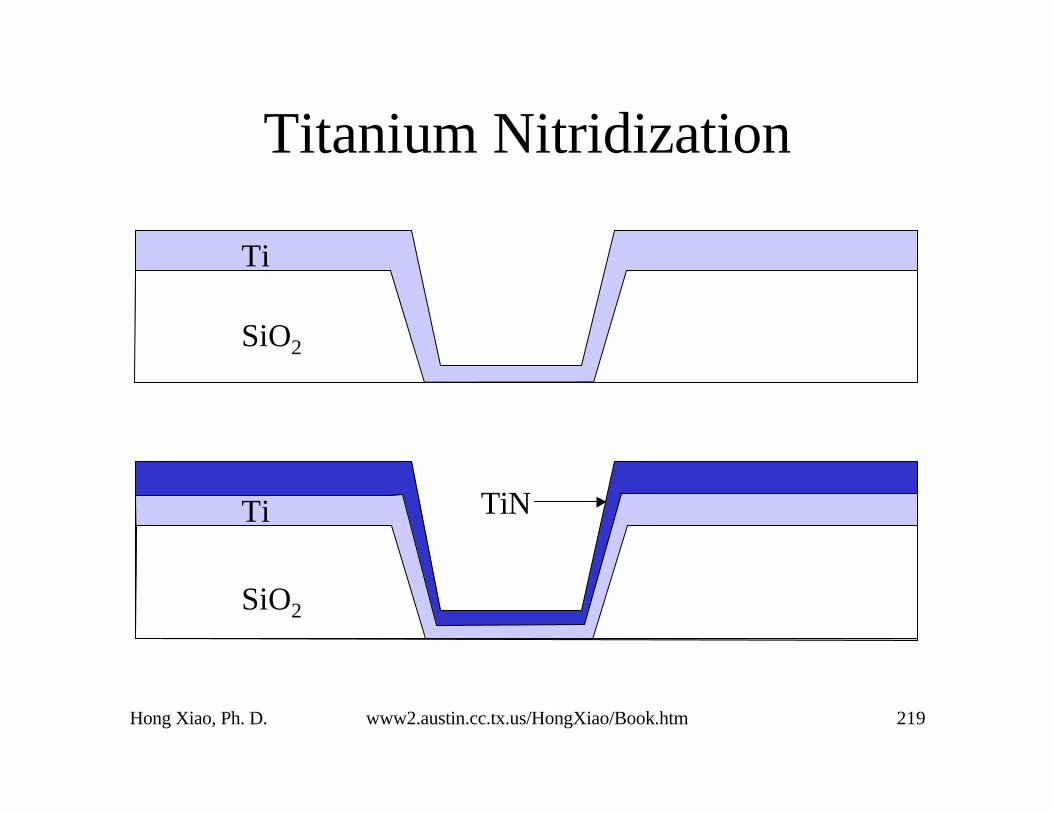
Thermal Nitridization
• Titanium PVD
• Thermal nitridization with NH3
NH3 + Ti → TiN + 3/2 H2
Hong Xiao, Ph. D. www2.austin.cc.tx.us/HongXiao/Book.htm 219
Titanium Nitridization
SiO2
SiO2
Ti
Ti TiN

Hong Xiao, Ph. D. www2.austin.cc.tx.us/HongXiao/Book.htm 220
RTO Process
• Ultra thin silicon dioxide layer < 30Å
• Better WTW uniformity
• Better thermal budget control

Hong Xiao, Ph. D. www2.austin.cc.tx.us/HongXiao/Book.htm 221
RTP Process Diagram
Time
Rampup 1& 2
Cooldown
RTALoadwafer
Unloadwafer
RTO
O2 flow
N2 flow
HCl flow
Temperature

Hong Xiao, Ph. D. www2.austin.cc.tx.us/HongXiao/Book.htm 222
Future Tends
• Rapid thermal process (RTP)
• In-situ process monitoring
• Cluster tools
• Furnace will still be used

Hong Xiao, Ph. D. www2.austin.cc.tx.us/HongXiao/Book.htm 223
RTCVD ChamberHeating Lamps
Wafer
QuartzWindow
Reactants
Reactants &byproducts
IR PyrometerWater CooledChamber Wall
Lamp Housing

Hong Xiao, Ph. D. www2.austin.cc.tx.us/HongXiao/Book.htm 224
Temperature of RTP & Furnace
Time
Tem
pera
ture
Time
Furnace
RTP
RoomTemp.

Hong Xiao, Ph. D. www2.austin.cc.tx.us/HongXiao/Book.htm 225
Cluster Tool
TransferChamber
RTCVDα-Si
Loading Station
HF VaporClean
RTO/RTP
Cooldown
Unloading Station

Hong Xiao, Ph. D. www2.austin.cc.tx.us/HongXiao/Book.htm 226
Summary of RTP
• Fast
• Better process control– Thermal budget
– Wafer to wafer uniformity
• Minimized dopant diffusion
• Cluster tool, easy process integration

Hong Xiao, Ph. D. www2.austin.cc.tx.us/HongXiao/Book.htm 227
Summary of Thermal Process
• Oxidation, diffusion, annealing, and deposition
• Wet oxidation is faster, dry oxidation has betterfilm quality. Advanced fab: mainly dry oxidation.
• Diffusion doping with oxide mask, used in lab
• LPCVD polysilicon and front-end silicon nitride
• Annealing recovers crystal and activates dopants
• RTP: better control, faster and less diffusion
• Furnaces: high throughput and low cost, willcontinue to be used in the future fabs