Chapter 5 : Electronics - ANTARESantares.in2p3.fr/Publications/TDR/v1r0/Chap5_Electronics.pdf ·...
100
Chapter 5 : Electronics Introduction ● DAQ and Slow-control function ● Power Distribution ● Clock Distribution ● Trigger distribution ● Hardware Implementation ● Reliability, qualification and Accelerated Stress tests ● Test benches and test scenarios ● Electronics PBS and Individual Object Description PBS 2.1 LCM Local Control Module: electronics of a Storey ❍ PBS 2. 2 SCM String Control Module: DAQ/SC, clock distribution, sensors, acoustic positioning ❍ PBS 2.3 SPM String Power Module: power conversion for each string ❍ PBS 2.4 JB Junction Box: Clock distribution and trigger construction ❍ PBS 2.5 ONSHORE Clock : Clock objects on shore ❍ ● Page 5-1
Transcript of Chapter 5 : Electronics - ANTARESantares.in2p3.fr/Publications/TDR/v1r0/Chap5_Electronics.pdf ·...

Chapter 5 : Electronics
Introduction
DAQ and Slow-control function
Power Distribution
Clock Distribution
Trigger distribution
Hardware Implementation
Reliability, qualification and Accelerated Stress tests
Test benches and test scenarios
Electronics PBS and Individual Object DescriptionPBS 2.1 LCM Local Control Module: electronics of a Storey
PBS 2. 2 SCM String Control Module: DAQ/SC, clock distribution, sensors, acousticpositioning
PBS 2.3 SPM String Power Module: power conversion for each string
PBS 2.4 JB Junction Box: Clock distribution and trigger construction
PBS 2.5 ONSHORE Clock : Clock objects on shore
Page 5-1
Contents
Electronics Introduction
The main purpose of the ANTARES electronics is to provide a hardware implementation inwhich the following functions can be performed:
data acquisition/slow control,
power distribution,
clock distribution,
trigger distribution
Technical aspects (mechanics, connections, thermal cooling) concerning all the boards aredescribed in the section on Hardware implementation. The reliability of the offshore electronics isan important issue and requires careful choice of components and testing of the electronics prior todeployment.
The electronics are located in various pressure resistant containers of the detector architecture assummarised in the line structure page or PBS. Six main objects are relevant, for the electronicsdiscussion:
The Local Control Modules (LCM) PBS2.1 contain the electronics for the readout of threeOptical Modules (OM) and the various instruments located on a storey. They also containthe electronics of the offshore trigger logic and the local power supply. One LCM, calledMaster Local Control Module (MLCM), is present in every sector and multiplexes inaddtion, the signal information from five storeys onto one optical fibre at a wavelengthunique to that Storey.
The String Power Module (SPM) PBS2.3 contains the power supply for the string.
The String Control Module (SCM) PBS2.2 contains the electronics for the readout andcontrol of the SPM and the instruments located at the bottom of the string.
The Junction Box (JB) PBS2.4 is the central point of the detector; it has connections to alldetector strings and to shore. It contains the power supply for the whole detector and theelectronics for conversion of the trigger signals into a global readout request signal. It alsodistributes the clock signals to all LCMs.
The electronics for the generation of the master clock (PBS2.5) is located at the shorestation. The main power supply is also located onshore, in the power hut.
Each detector string consists of 1 SPM, 1 SCM and 30 LCMs. The LCMs inside a string areorganised in 6 sectors; each sector consists of 5 LCMs. Each sector has a master LCM whichcombines the functionality of a LCM with that of network node in the offshore DAQ system.
Within each of these containers, a number of electronics cards provide the desired functionality,which are described in the individual object PBS pages. The electronics cards are inserted in a crateand the power and signals are passed between boards via the backplane or via twisted pair wires.
Page 5-2

The connection between the various containers are provided by electro-optical cables, the powerbeing transmitted via electrical wires and the signals via optical fibres.
The most relevant technical notes are listed at the end of each section.
Page 5-3

DAQ and Slow-control functions
The data acquisition and slow-control functions are described in chapter 4. The electronicsimplementation is described here. The readout chain is summarised in the figure below.
Functional schematic of the DAQ electronics
The analog output signal of each PMT is processed by two Analogue Ring Sampler (ARS) chipslocated on the ARS motherboard (ARS_MB). The ARS produces a time-stamped digitisation of thePMT signal. Two digitisation modes are possible: Single Photo Electron (SPE) and WaveForm(WF). A SPE event contains only the total charge of the PMT signal, whereas the WF contains alsoa waveform sampling of the PMT output.
When a L1 or L2 trigger (for a definition, cf Chapter 4 on offshore trigger) is received, the ARSbegins the digitisation of the analog signal inside the analog pipeline for WF sampling or internalcharge integration for the SPE event; the resulting digital data packet is sent over the chip serialoutput to the DAQ board. If no trigger is received within a fixed latency, the signal is discarded.
The bandwidth of the readout system is increased using a Dense Wavelength DivisionMultiplexing (DWDM) and Ethernet switches. Its implementation is summarised in Figure 2.
Page 5-4

Figure 2: The offshore DWDM system
At the DAQ board of an LCM (LCM_DAQ/SC) the data produced by three ARS motherboardsis transmitted using the BIDIANT transceiver board, via optical fibre (1310 nm) to the MLCM. Atthe MLCM, the data from the five LCMs (MLCM + four slaves) are received by a bi-directionalEthernet concentrator board (LCM_BIDICON) and the optical signals are converted to electrical
Page 5-5

signals. The signals are passed via the backplane to the MLCM_SWITCH board where the five setsof signals are combined and then passed via coaxial SMB connectors to the MLCM_DWDM board.This board converts the gigabit Ethernet signals into optical signals of a DWDM system (1535nm-1570 nm) and sends them to the SCM.
Figure 3: The onshore DWDM system
Page 5-6
At the SCM, the optical signals from the six MLCMs of a string, are received by a passive opticalmultiplexer (SCM_DWDM_MUX) and combined onto a single fibre, each MLCM having itsunique pair of wavelengths. The Slow Control information is also included in the wavelengthmultiplexing as a seventh wavelength. In order to do this, the Slow Control information passesthrough the SCM_DWDM board prior to inclusion. The data then passes through the Junction Boxto the shore station. An equivalent system on shore, demultiplexes the wavelengths as shown infigure 3.
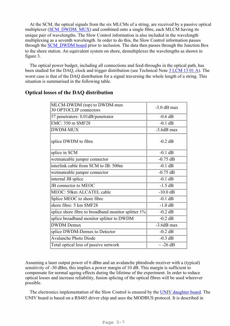
The optical power budget, including all connections and feed-throughs in the optical path, hasbeen studied for the DAQ, clock and trigger distribution (see Technical Note 3 LCM 13 01 A). Theworst case is that of the DAQ distribution for a signal traversing the whole length of a string. Thissituation is summarised in the following table.
Optical losses of the DAQ distribution
MLCM-DWDM (top) to DWDM-mux 30 OPTOCLIP connectors -3.0 dB max
57 penetrators: 0.01dB/penetrator -0.6 dBEMC: 350 m SMF28 -0.1 dBDWDM-MUX -3.6dB max
splice DWDM to fibre -0.2 dB
splice in SCM -0.1 dBwetmateable jumper connector -0.75 dBinterlink cable from SCM to JB: 500m -0.1 dBwetmateable jumper connector -0.75 dBinternal JB splice -0.1 dBJB connector to MEOC -1.5 dBMEOC: 50km ALCATEL cable -10.0 dBSplice MEOC to shore fibre -0.1 dBshore fibre: 5 km SMF28 -1.0 dBsplice shore fibre to broadband monitor splitter 1% -0.2 dBsplice broadband monitor splitter to DWDM -0.2 dBDWDM Demux -3.6dB maxsplice DWDM-Demux to Detector -0.2 dBAvalanche Photo Diode -0.3 dBTotal optical loss of passive network ~ -26 dB
Assuming a laser output power of 6 dBm and an avalanche phtodiode receiver with a (typical)sensitivity of -30 dBm, this implies a power margin of 10 dB. This margin is sufficient tocompensate for normal ageing effects during the lifetime of the experiment. In order to reduceoptical losses and increase reliability, fusion splicing of the optical fibres will be used whereverpossible.
The electronics implementation of the Slow Control is ensured by the UNIV daughter board. TheUNIV board is based on a RS485 driver chip and uses the MODBUS protocol. It is described in
Page 5-7
detail in the technical notes 3 LCM 08 01/A and 3 LCM 08 02/A. The instruments which have aRS232 link require a dedicated bridge.
Technical notes are available for more details:3 LCM 15 01A: ARS motherboard description.
3 LCM 05 01 A: LCM_DAQ/SC board description
3 LCM 13 01 A: Design specifications for the ANTARES DAQ- DWDM Network- Part I
3 LCM 13 02 A: Design specifications for the ANTARES DAQ- DWDM Network- Part II
3 LCM 20 01 A: LCM internal organisation
ANTARES-Elec/2000-6: ARS1 Analogue Ring Sampler & ARS_CONV Users ManualVersion 1.9
3 LCM 08 01/A UNIV1 board user's manual
3 LCM 08 02/A. MODBUS protocol reference guide.
Page 5-8
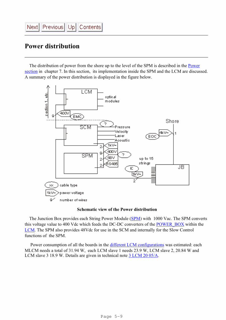
Power distribution
The distribution of power from the shore up to the level of the SPM is described in the Powersection in chapter 7. In this section, its implementation inside the SPM and the LCM are discussed.A summary of the power distribution is displayed in the figure below.
Schematic view of the Power distribution
The Junction Box provides each String Power Module (SPM) with 1000 Vac. The SPM convertsthis voltage value to 400 Vdc which feeds the DC-DC converters of the POWER_BOX within theLCM. The SPM also provides 48Vdc for use in the SCM and internally for the Slow Controlfunctions of the SPM.
Power consumption of all the boards in the different LCM configurations was estimated: eachMLCM needs a total of 31.94 W, each LCM slave 1 needs 23.9 W, LCM slave 2, 20.84 W andLCM slave 3 18.9 W. Details are given in technical note 3 LCM 20 05/A.
Page 5-9

Clock Distribution
The main purpose of the clock system is to provide a common clock signal to all ARSs. Itconsists of a clock generator on shore, a clock distribution system and a clock signal transceiver ineach LCM. In addition, it can distribute a (small) number of other commands to the LCMs. Thesecommands can be addressed to a single LCM or to all LCMs simultaneously. The same clock is alsoused by the acoustics positioning system.
The main specifications of the clock system are:generation of a 20 MHz clock signal
Distribution of the (common) clock signal to all LCMs
Distribution of (synchronised) data commands for common orders like DAQ start or stoprun.
Time stability better than 0.5 ns
Time correlation with the GPS time better than 100 ns.
Possibility to measure delay propagation between on shore to each LCM or SCM containerwith a precision better than 1 ns, for time calibration.
The clock system is based on the network synchronisation concept used in thetelecommunications industry in which digital data are superimposed on a high frequency referenceclock. The combined signal is sent to the detector and distributed to all LCMs. In each LCM theoriginal clock signal and the data are decoded.
A functional diagram of the clock system is shown below. The reference clock is generated onshore (ON_GPS) using a high accuracy 20 MHz clock synchronised internally to the GPS time withan accuracy of 100 ns. The clock is passed to the ON_CLOCK board where any clock commandsare superimposed. The clock electrical signal is converted to an optical signal in the ON_WDMboard which transmits the signal to the Junction Box, via a single optical fibre, using standardtelecommunication transceiver chips (HOTLINK chips from Cypress company). With thisconfiguration, the time jitter was measured to be less than 100 ps.
A passive splitter inside the Junction Box (JB_SPLIT1) divides the optical clock signal into 16different channels, one for each string (plus spares). Inside the SCM, an Optical/Electricalconversion (SCM_WDM) regenerates the signal and an Electrical/Optical conversion (SCM_REP)sends the clock signal to the LCM_CLOCK board of each LCM container. The LCM_CLOCKboard reconstructs the clock and decodes any associated command, making them available on theLCM backplane.
Page 5-10
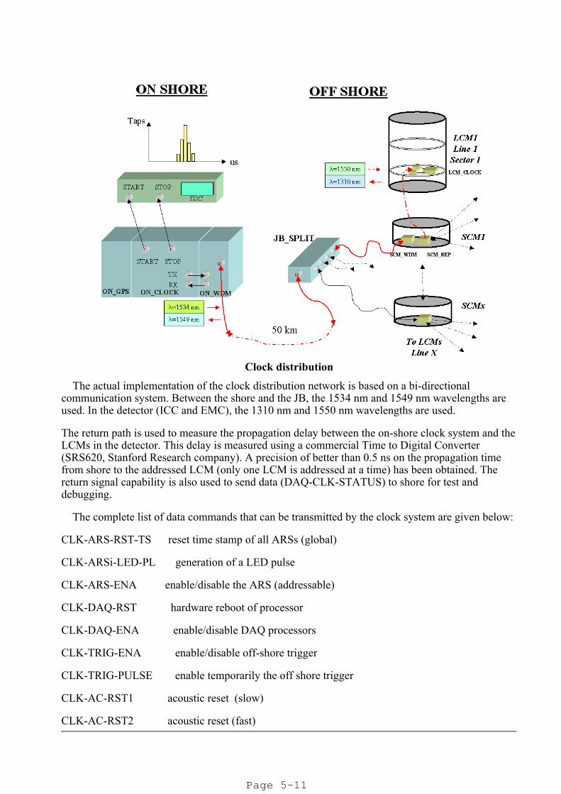
Clock distribution
The actual implementation of the clock distribution network is based on a bi-directionalcommunication system. Between the shore and the JB, the 1534 nm and 1549 nm wavelengths areused. In the detector (ICC and EMC), the 1310 nm and 1550 nm wavelengths are used.
The return path is used to measure the propagation delay between the on-shore clock system and theLCMs in the detector. This delay is measured using a commercial Time to Digital Converter(SRS620, Stanford Research company). A precision of better than 0.5 ns on the propagation timefrom shore to the addressed LCM (only one LCM is addressed at a time) has been obtained. Thereturn signal capability is also used to send data (DAQ-CLK-STATUS) to shore for test anddebugging.
The complete list of data commands that can be transmitted by the clock system are given below:
CLK-ARS-RST-TS reset time stamp of all ARSs (global)
CLK-ARSi-LED-PL generation of a LED pulse
CLK-ARS-ENA enable/disable the ARS (addressable)
CLK-DAQ-RST hardware reboot of processor
CLK-DAQ-ENA enable/disable DAQ processors
CLK-TRIG-ENA enable/disable off-shore trigger
CLK-TRIG-PULSE enable temporarily the off shore trigger
CLK-AC-RST1 acoustic reset (slow)
CLK-AC-RST2 acoustic reset (fast)
Page 5-11

Details of this clock distribution are described in the technical notes:3 LCM 03 01/C: Numerical clock distribution proposal
3 LCM 03 02/A: Clock board interface
3 LCM 18 02/A: Clock distribution prototype tests
3 LCM 20 01/A: BIDIANT user manual
Page 5-12

Trigger system
The offshore trigger is described in detail in chapter 4, the electronics implementation ispresented here.
The offshore trigger allows the selection of a subsample of the total data flow for digitisation,transmission and processing on shore. The trigger is based on time coincidences of signals betweenoptical modules of the same storey and also between adjacent storeys.
In order to construct the trigger, the ARS mother board (ARS_MB) produces signalscorresponding to whether the output of the each of the three PMTs has passed a lower threshold(L0) or a higher (L00) threshold (the thresholds are programmable via Slow Control). These signalsare sent, via the LCM backplane, to the LCM trigger board (LCM_TRIG). Here a decision, basedon time coincidences between the six set of signals, is made as to whether to read out just the localtriplet of OMs (a L1 trigger) or to initiate a global readout request (L2 trigger).
If a L2 trigger is generated it is passed, via the SCM, to the Junction Box trigger board(JB_TRIG1). Here, the L2 triggers from all lines are optically merged (ORed) using a passiveoptical splitter. The output of the splitter is regenerated (using a BIDITRIG board) and retransmittedat a different wavelength, through the same optical splitter back to all the LCMs as the Read OutRequest (RoR).
The trigger construction in the LCM trigger board (LCM_TRIG) is performed using a FieldProgrammable Gate Array (FPGA). A local oscillator (100 MHz) is used to generate the delays andpulse widths for the various trigger signals with a precision of 10 ns. All the necessary triggerrequirements, delays and pulse widths are definable by Slow Control using the UNIV1 board.
The L1 signal from an upper storey is passed via a single optical fibre to a lower storey, where itcan also be used in the construction of the L2 trigger decision of that storey.
The L2 and RoR signals are bi-directional on one optical fibre of the EMC. The L2/RoR opticalfibre is daisy chained the whole length of a string. As the signals propagate down (L2) or up (RoR)the EMC cable, they pass through many other LCM_TRIG boards and are regenerated each time ina BIDITRIG daughter board.
Two optical fibres (plus two spares) in the Main Electro-Optical Cable (MEOC), are used to testand monitor the offshore trigger. They are connected to the JB_TRIG board of the JB.
Page 5-13

Schematic view of the offshore trigger.
Page 5-14

Hardware implementation
The Electro-Mechanical Cable
The connections between the SCM and the LCM are made by the electro-mechanical cable(EMC). It comprises 9 copper wires for power distribution and 21 optical fibres for datatransmission.
For the DAQ, each MLCM is connected to the SCM by one pair of optical fibres. Each LCM in asector is connected to its MLCM by a single (bidirectional) fibre. For the distribution of the clocksignal, the bottom LCM of a sector is connected to the SCM by a single fibre; the same fibre is usedto daisy-chain the signal through the sector. The L2 trigger and readout request signals aredaisy-chained through the entire string on a single (bidirectional) fibre. One additional fibre is usedto transmit the L1 trigger between storeys. The total number of fibres is thus 2*6 +1(daq+sc) + 6(clock) + 2 (trigger) = 21. A schematic of the fibre connections is shown below and can be seenbetter by clicking here on on the icon:
The electrical power distribution in the EMC has a similar organisation. The bottom LCM of eachsector is connected to the SPM by a single copper wire. The same wire is used to daisy-chain thepower distribution to the other LCMs of the same sector. The return current of two sectors iscombined into one copper wire. Thus, a total of 9 wires is is needed for the electrical powerdistribution on the string.
The connection between the SPM and the SCM passes through a sleeve joining the two modules.This allows the power in the SPM to be separated from the optical fibres in the SCM.
The Interconnecting Link
Each detector string is connect to the JB by an Interconnecting Link (IL); the interconnectingcable of the IL has 2 copper wires and 4 optical fibres. The copper wires are used to transfer powerfrom the JB to the SPM. The optical fibres transmit signals between the JB and the SCM; two fibresare used for the DAQ, one for the clock, and one fibre transmits both the L2 trigger and the readoutrequest.
The Main Electro Optical Cable
The JB is connected to shore by the Main Electro-Optical Cable (MEOC). The MEOC has 48fibres and one copper sheath. The sheath is used to distribute the power from the power hut; thereturn current flows through the sea water. For the DAQ, the JB connects each pair of optical fibresof a string to a corresponding pair of optical fibres in the MEOC. A single optical fibre (plus aspare) is used for the distribution of the clock signal. In addition, 2 optical fibres (plus 2 spares) are
Page 5-15

used to test and monitor the off-shore trigger system. The number of fibres in the MEOC issufficient to allow for a larger number of detector strings than presently foreseen.
Containers
The electronics boards are mounted in pressure-resistant titanium containers. A mechanicaldescription of the containers is given in chapter 2 on mechanics. Inside these containers, theelectronics boards are mounted on a common backplane. The boards are mounted perpendicular tothe backplane and can be exchanged independently. All boards have the same dimensions. Thefollowing figure shows the crate with the power supply and some boards.
Electronics crate prototype with inserted boards and the POWER_BOX
The thermal cooling of the electronics is ensured using copper screens inserted between theelectronics boards. These screens are in contact with the titanium container, maintained at theambient sea water temperature (14°) via flexible copper 'fingers'. Hot electronics components areconnected directly to these screens via a thermal bridge. Laboratory measurements show that athermal resistance of 17°/watt can be obtained using this method (see internal note 3 LCM18-04/A).
The copper screens have a secondary function of providing electromagnetic shielding betweensensitive analog functions such as the ARS motherboard (ARS_MB) and noisy digital functionssuch as the MLCM_SWITCH.
For the electrical connections, soldering is adopted in order to minimise the risk of oxidation ofconnector contacts. All connectors between the boards and the backplane are gold-plated.
For the optical connections, fusion splicing is adopted wherever possible. When necessary,optical connectors will be used (OPTOCLIP II). After qualification tests, connectors from theDeutsch company have been chosen; they have the following features:
Optical power loss: average 0.07 dB per connector (max 0.1 dB). For theworst case of a signal traversing the 30 connectors of a complete line, the
Page 5-16
maximum optical power loss is 3 dB.Reliability of plugging/unplugging: better than 0.05 dB
Reliability in time: better than 40 years
All the OPTCLIP II connectors are located on the LCM_OPTCON card.
Associated Technical Notes:
3 LCM 13 01 A Design Specifications for the ANTARES optical DAQ-DWDM Network,Part I.
3 LCM 18 04/A Thermal tests for LCM container
3 LCM 20 01/A LCM internal organisation, for the electronics function implementationinside this container.
3 SCM 20 01/A SCM internal organisation, for the electronics function implementationinside this container.
3 LCM 20 02/A LCM/SCM boards mechanical dimensions and backplane connectorimplementation.
Page 5-17

Page 5-18

Reliability, Qualification and Accelerated Stress Test
The reliability of the offshore electronics is crucial for the long term operation of the detector.The objectives for the overall reliability of the detector are discussed in Chapter 10.
There are three ways to optimise the reliability of the off-shore electronics:Choose the components in order to have the best mean time between failure, compatiblewith availability, price and power requirements
Require that all designs pass an electronics qualification test before adoption, based on theexpected environmental life profile.
Define a common burning test scenario in order to eliminate bad manufacturing and infantmortality.
Electronics qualification
In order to improve the reliability, the environmental life profiles of the embedded electronics havebeen studied, resulting in the following qualification tests for the design, which will be verified onthe first boards:
Cold temperature: Storage at 0°C in a wooden crate during transport
Dry heat: storage at 60°C in a crate during transport, working a few minutes at + 40°Cwithout its packaging.
Damp heat: storage at 50°C and 93% relative humidity (RH), container open
Condensation: Damp heat at +40°C and 93% (RH), container open
Immersion: Working at 3 metres depth, in 25°C seawater for 24 hours.
Salt fog: Container closed, on quay for one month with 50°C and 1000 W/m².
Rain: container closed, on quay for one month
Thermal shocks: From 50°C air to 15°C seawater.
Sinusoidal vibrations (transport simulation): 5-55 Hz on container without packaging.
Half-sinusoidal shocks of 15 g acceleration and 50 Hz on container.
Free fall: height 700 mm on metallic or concrete floor.
Changes in the external appearance of objects can be tolerated as far as they do not impair thefunctionalities of the object. The first electronics boards must pass these qualification criteria.
The qualification program is described in technical note: 3 LCM 20 04/A.
Accelerated Stress Testing scenario (AST)
The overwhelming majority of electronics failures are latent (hidden) manufacturing defects.Once a robust design has been qualified, testing for reliable field operation can be done much fasterand cost-effectively under stress levels that exceed the end-use specifications. An efficient stressscreen is to simulate one year of a product's overall fatigue lifetime. This should eliminate 90% ofthe front-end life cycle `bathtub curve' of `infant mortality' leaving more than 20 years of `normaluse' fatigue lifetime in the product.
Page 5-19

The following AST scenario is applied to all electronics cards before integration inside any cratecontainer ( cf also 3_LCM 20 04/A.):
Temperature cycling from 10°C to 40°C, 4 cycles during 2 hours
Vibration with 3 g acceleration during 30 mn with 50 Hz frequency.
Reference technical note :
3 LCM 20 04/A. Electronics qualification and AST scenario
Page 5-20

Test Benches and test scenarios
In parallel with the electronics development, the development of the associated test benches andtest scenarios is necessary. The tests performed during fabrication and integration can be dividedinto three main types:
Test scenarios for each board during the prototype phase: every designer provides a testprocedure which describes the test set-up and the measurements along with the necessarysoftware and hardware. An example of this test scenario for the clock distribution functioncan be found in the Web link: 3 LCM 18 02/A Clock Distribution Prototypes Tests.
Manufacturer acceptation tests: each board realised by the manufacturer or a laboratory mustpass a test scenario before acceptation. These tests verify each function of the board andincorporate burning tests (AST scenario). The results of these acceptation tests are directlyentered on the Web pages (one per electronics board or object), in order that the results canbe incorporated in the general database.
Main objects integration tests: After the acceptation test of each board, the integration startswith insertion of boards inside the electronics crates. After integration of all these boards,the functionality of the total electronics crate is checked in a test bench, developed tomeasure and test this complete object. The results of these tests are also entered on the Webpages for incorporation into the general database.
Examples of complete test benches are:LCM test bench scenario and for summary web page: LCM test bench schematic
SCM test bench scenario and for summary web page: SCM test bench schematic
After integration of the electronics boards inside the containers, these final objects are sent forline integration. During the line integration of each LCM container, the good functionality of theelectronics and the connections between all objects are tested. These results are also incorporated inthe general database.
Page 5-21
PBS
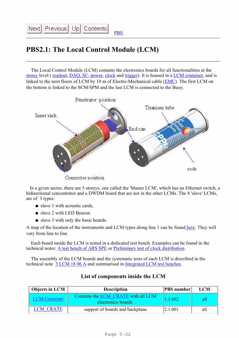
PBS2.1: The Local Control Module (LCM)
The Local Control Module (LCM) contains the electronics boards for all functionalities at thestorey level ( readout, DAQ, SC, power, clock and trigger). It is housed in a LCM container, and islinked to the next floors of LCM by 10 m of Electro-Mechanical cable (EMC). The first LCM onthe bottom is linked to the SCM/SPM and the last LCM is connected to the Buoy.
In a given sector, there are 5 storeys, one called the 'Master LCM', which has an Ethernet switch, abidirectional concentrator and a DWDM board that are not in the other LCMs. The 4 'slave' LCMs,are of 3 types:
slave 1 with acoustic cards,
slave 2 with LED Beacon
slave 3 with only the basic boards.
A map of the location of the instruments and LCM types along line 1 can be found here. They willvary from line to line.
Each board inside the LCM is tested in a dedicated test bench. Examples can be found in thetechnical notes: A test bench of ARS SPE or Preliminary test of clock distribution.
The assembly of the LCM boards and the systematic tests of each LCM is described in thetechnical note 3 LCM 18 06 A and summarised in Integrated LCM test benches.
List of components inside the LCM
Objects in LCM Description PBS number LCM
LCM Container Contains the LCM_CRATE with all LCMelectronics boards 1.3.002 all
LCM_CRATE support of boards and backplane 2.1.001 all
Page 5-22

LCM_BACK distributes signals between boards inLCM_CRATE 2.1.002 all
COMPASS_MB measures positions with compass andtiltmeters,controls PMT HV 2.1.003 all
ARS _MB Motherboard with 3 ARS1 chips 2.1.004 all
ARS1 analog pipeline with ADC conversion of PMTsignal 2.1.004.1 all
MLCM_BIDICON Concentrates 4 optical transceivers from eachLCM slave DAQ channel 2.1.005 MLCM only
LCM_TRIG Receives trigger from ARS boards andconstructs trigger function 2.1.006 all
LCM_CLOCK receives optical clock distribution signal anddistributes inside LCM crate 2.1.007 all
ACOUST_RX
_PREAMPPositioning system 2.1.008 slave 1 only
ACOUST_RX
_DSPPositioning system 2.1.009 slave1 only
ACOUST_RX
_CPUPositioning system 2.1.010 slave1 only
POWER_BOX Converts 400V to needed voltages 2.1.011 all
LCM_OPTCON Optical and electrical connections between maincable and LCM_CRATE 2.1.012 all
UNIV1 Daughter board plugged on other board for slowcontrol MODBUS interface 2.1.013 all
BIDIANT Daughter optical transceiver board for Ethernetand Clock signals 2.1.014 all
BIDITRIG Daughter optical transceiver board for triggersignals 2.1.015 all
MLCM_DWDM DWDM transceiver board with laser, receiverand DWDM filter 2.1.016 MLCM only
LCM_DAQ/SC Data and slow control board which sends andreceives Ethernet Protocol 2.1.017 all
MLCM_ SWITCH Gbit switch 2.1.018 MLCM only
List of references
http://antares.in2p3.fr/internal/deci-km2/tableaux/LCM and all references in that table, in particulartechnical note 3 LCM 20 01/A describing the LCM internal organisation
Page 5-23

MasterLCM/SlaveLCM Test Bench
Schematic view of the LCM Test Bench
The Test Bench consists of a main computer connected with a set of instruments and devices.Each single board within the Design Under Test (DUT) is assumed to be already tested.
Specifications:
The aim of the Test Bench is to test the overall functionality of SLCM/MLCM seriesproduction.
The results of the tests must be logged in order to ensure quality documents.
All the DUT communication links must be tested. These are:
Page 5-24

Physical signals from OMs, LED ball and hydrophones;
100 Mb Ethernet DAQ/SC optical link between Master and Slave LCMs;
1 Gb Ethernet DAQ/SC optical link (only MLCM);
L1 and L2/RoR Trigger optical links;
Clock optical link.
Test points inside the DUT must also be provided monitoring electrical parameters ofinterest.
Interfaces with DUT are:
LCM_TRIG board in order to test the L2 “2 storey” Trigger capability.
LCM_DAQ/SC board for Master/Slave communication test.
LCM_SWITCH board for Ethernet communications with Master LCM.
Technical Notes: 3 LCM 18 06 A LCM Test Bench
Page 5-25

PBS 2.1.001 : LCM_CRATE(inside LCM container)
Schematic view of the inner rack
Description:
The LCM_CRATE inner rack is housing the electronics embarked on the lines.
It consists of an axial structure that links all the cards and the backplane
Electric and optical cables penetrate the container and are plug in cards.
This structure looks like a cylindrical cage placed inside the LCM container and fixed in thelower bottom end cap by a crown.
Dimensions, technological features:
Effective inner diameter: 155 mm
Effective inner length: 550 mm
The selected material for all part of the inner rack is aluminium 2017. Both inner and outerdiameters must be chamfered
Interfaces inside LCM are:
Page 5-26

16 boards
1 electrical connection board
1 optical connection device
LCM power box for voltage
4 shieldings for OEM and thermal conduction
Technical notes:
3 LCM 02 01:Integration LCM
3 LCM 02 03: shielding
3 LCM 02 04: crown 1
3 LCM 02 05: crown 2
3 LCM 02 06: Slides
Page 5-27
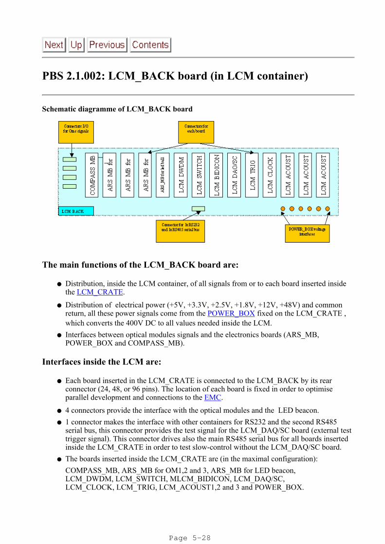
PBS 2.1.002: LCM_BACK board (in LCM container)
Schematic diagramme of LCM_BACK board
The main functions of the LCM_BACK board are:
Distribution, inside the LCM container, of all signals from or to each board inserted insidethe LCM_CRATE.
Distribution of electrical power (+5V, +3.3V, +2.5V, +1.8V, +12V, +48V) and commonreturn, all these power signals come from the POWER_BOX fixed on the LCM_CRATE ,which converts the 400V DC to all values needed inside the LCM.
Interfaces between optical modules signals and the electronics boards (ARS_MB,POWER_BOX and COMPASS_MB).
Interfaces inside the LCM are:
Each board inserted in the LCM_CRATE is connected to the LCM_BACK by its rearconnector (24, 48, or 96 pins). The location of each board is fixed in order to optimiseparallel development and connections to the EMC.
4 connectors provide the interface with the optical modules and the LED beacon.
1 connector makes the interface with other containers for RS232 and the second RS485serial bus, this connector provides the test signal for the LCM_DAQ/SC board (external testtrigger signal). This connector drives also the main RS485 serial bus for all boards insertedinside the LCM_CRATE in order to test slow-control without the LCM_DAQ/SC board.
The boards inserted inside the LCM_CRATE are (in the maximal configuration):
COMPASS_MB, ARS_MB for OM1,2 and 3, ARS_MB for LED beacon,LCM_DWDM, LCM_SWITCH, MLCM_BIDICON, LCM_DAQ/SC,LCM_CLOCK, LCM_TRIG, LCM_ACOUST1,2 and 3 and POWER_BOX.
Page 5-28

PBS 2.1.3 : COMPASS_MB board (in LCM and SCMcontainers
Schematic view of the COMPASS_MB board
The main specifications of the COMPASS_MB board are:
Controls the Tilt compass daughter board with a RS485 MODBUS protocol and RS232 tiltcompass daughter board bridge.
Measures the humidity sensor which is included on the board for humidity control insideLCM and SCM containers.
Measures temperature sensors (2 on the board)
Reads the temperature sensors which are plugged on ARS_MB cards (1 temperature sensorfor each ARS_MB : 3 sensors + 1 from ARS_MB LED if present).
Controls the low voltage command of the high voltage of each optical module with 12 bitsDAC with a 0 to 4 volts range (3 voltage commands).
Measures the low voltage command value at the output of the DAC (3 voltage values)
All these controls and measurements are performed through 2 UNIV1 functions with twodifferent MODBUS addresses.
Interfaces inside LCM are:
Page 5-29

The standard interface is a 24 pins connector, all signals come from the backplane via theLCM_BACK board.
List of references
3LCM_07_01A : technical note of COMPASS_MB
PBS 5.6 Humidity sensor
PBS 5.2 Tilt meter and compass daughter board
Page 5-30

PBS 2.1.004: ARS_MB board (in LCM/MLCM container)
Schematic of the ARS motherboard
The main functions of the ARS_MB board are:
Interface of the 3 ARS chips to the LCM_DAQ/SC board. ARS#0 and ARS1#1 are used forsignal processing, ARS#2 is used to generate of supplementary anode impulse trigger signal(L00) with its separate, slow control set, trigger level (th2)
Passing of the token between ARS1#0 and ARS1#1
Generation of LED pulser pulse and peak value reference voltage (0-24 V).
Use of attenuated LED pulser pulse for re-injection in the anode for LCM tests withoutOptical Modules
Page 5-31

Interfaces inside LCM:
POWER BOX (~2W total): +48 V (2mA), +12 V (4mA), +6 V (160 mA), + 5V(160mA), +5V(1mA), +3.3 V (250 mA), GND.LCM_TRIG: L0, L00, and L1, L2 (LVDS signals).
LCM_CLOCK: ACLK, WREF_CLK (5 MHz), EN_ACK, RES_TS (LVDS signals),LED_PL (LVDS signals).
LCM_DAQ/SC: CLK_OUT (40 MHz), READOUT1, READOUT0, CRMW (LVDSsignals). ARS_RESET, SC_VALID, SC_CLK (CMOS/LVTTL signals), SC_DATA(bi-directional CMOS out, CMOS/LVTTL in), SC_OE (determines direction of SC_data forI/O buffer), WCLK_ERROR (open collector signal weakly pulled up to 5 volt onLCM_ARS board).
COMPASS: ARS_COMPASS_temp (analogue)
Interfaces to OM:
LED_PL (twisted pairs) through back-plane connector.
PMT anode and dynode signals via screened twisted pairs. there will be space at the far endof the backplane, where the incoming OM_LCM link will be connected to a cable going tothe ARS_MB connector (type of connector MCX, type of cable RG178, 4 cables perARS_MB).
Associated Technical Notes:
3 LCM 15 01 ARS motherboard
Page 5-32

PBS 2.1.004.1: The Analogue Ring Sampler Chip (on ARSmotherboard)
Schematic of the ARS signal processing
The Analogue Ring Sampling chip performs the off-shore processing of the PMT signals. It islocated on the ARS motherboard of a LCM container.
The anode signal is sent to the comparator, the charge integrator, the Pulse Shape Discriminator,and the GHz waveform sampler. When a pulse exceeds the L0 trigger threshold of the comparator,its charge is integrated and the waveform is sampled while the PSD analyses the pulse shape andcompares it to the predefined mask. At the end of the integration gate, the PSD returns the binaryresult whether the pulse is of the SPE type or the Waveform (WF) type. The timing of the signals isgiven by an external reference clock; the Time Stamp (TS) counts the reference clock pulses, andthe Time-to-Voltage Converter (TVC) provides an analogue signal proportional to the time fromthe last clock signal to the instant when the pulse crossed the L0 threshold.
A pipeline memory is used to store the analogue and digital data. The pipeline consists of 16memory cells to store up to 16 pulses. Each memory cell contains two analogue values (theintegrated charge and the TVC) and 26 bits of digital data (the 24-bit Time Stamp, the 1-bit PSDresult, and 1 bit to indicate if WF data has effectively been sampled). Once this information hasbeen stored in the pipeline, the comparator, the integrator, and the TVC and Time Stamp functionsare freed for the next pulse, without waiting for the digitisation of the pulses in the pipeline.
Page 5-33

Waveform data is stored outside the pipeline. The GHz waveform sampler has four synchronouschannels, sampling the reference clock, the anode signal, an attenuated anode signal, and a dynodesignal. When a WF hit is found, the waveform sampling continues until 128 samples have beenstored for each of the four fast-sampling channels; then the sampler is blocked until these data aredigitised or discarded. If a WF event arrives when the WF sampler is occupied, the pulse will betreated as a SPE pulse with a flag indicating that the waveform sampler was not available.
The Time Stamp is used to determine if a pulse is in a trigger readout window. If a readoutrequest is received, the memory cell is read out, the charge and the TVC are each converted to 8-bitdigital values, and the digital information for the event, with a header added, is formatted fortransmission to shore. For WF events, the 128 clock samples and the corresponding 128 anode pulsesamples are converted to digital form and added to the event packet for transmission. For very largepulses, all four waveform channels are digitised : 128 samples each for the clock, the anode, theattenuated anode, and the dynode signals. If no readout request is received within a predefined lapseof time, the memory cell and the fast-sampling cells (in the case of a WF event) are erased andmade available for subsequent pulses.
The main functions of the ARS chip are:Measurement of time of arrival and integrated charge of Single Photon Electron (SPE) PMTsignals if confirmed by the trigger signals L1 or L2.
Pulse shape discrimination (PSD) to separate SPE events from NON-SPE (waveform)events.
Digitisation of waveform events measuring PMT anode, attenuated anode and dynodesignals as well as the sinusoidal time reference clock (band filtered ACLK clock signal).
Generation of L0 signal when PMT anode signal crosses threshold th1.
Generation of Counting Rate Monitor Warning (CRMW) signal set to go off at a determinedPMT pulse rate.
Generation of WCLK_ERROR if the waveform digitizer Delay Locked loop (DLL) isunlocked.
ARS Specifications:
Parameter Min spec. Max spec. Expected value Characteristics
Vsup 4.75 V 5.25 V 5 V Operating power supplies range.
Dsup +/-25 mV Power supplies drift, other than ADC.
Dsupadc +/-1 mV ADC power supply drift (vdd_adc).
T 0°C 50°C 15°C Operating temperature.DT +/-3°C Temperature drift.
Psup 250 mW 200 mW Power consumption of the ARS1 5-V supplies.
Fs 300 MHz 1 GHz Waveform mode sampling frequency.
Nc 4 Number of Waveform mode channels : anode, twointermediate gain channels (dynodes), and Aclk clock.
Ns 128 Number of Waveform mode samples per ARS1.
NARS 1 4 2 Number of ARS1 chips in the token ring.
VSPE 60 mV (13 pC) Single photoelectron pulse amplitude at the ARS1input.
Dadd 1.5 V 3.5 V Dynamic range of the anode, dynode1 and dynode2Waveform mode inputs.
Page 5-34
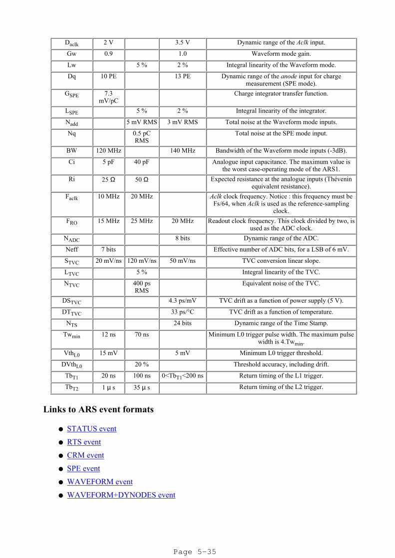
Daclk 2 V 3.5 V Dynamic range of the Aclk input.
Gw 0.9 1.0 Waveform mode gain.
Lw 5 % 2 % Integral linearity of the Waveform mode.
Dq 10 PE 13 PE Dynamic range of the anode input for chargemeasurement (SPE mode).
GSPE 7.3mV/pC
Charge integrator transfer function.
LSPE 5 % 2 % Integral linearity of the integrator.
Nadd 5 mV RMS 3 mV RMS Total noise at the Waveform mode inputs.
Nq 0.5 pCRMS
Total noise at the SPE mode input.
BW 120 MHz 140 MHz Bandwidth of the Waveform mode inputs (-3dB).
Ci 5 pF 40 pF Analogue input capacitance. The maximum value isthe worst case-operating mode of the ARS1.
Ri 25 Ω 50 Ω Expected resistance at the analogue inputs (Théveninequivalent resistance).
Faclk 10 MHz 20 MHz Aclk clock frequency. Notice : this frequency must beFs/64, when Aclk is used as the reference-sampling
clock.FRO 15 MHz 25 MHz 20 MHz Readout clock frequency. This clock divided by two, is
used as the ADC clock.NADC 8 bits Dynamic range of the ADC.
Neff 7 bits Effective number of ADC bits, for a LSB of 6 mV.
STVC 20 mV/ns 120 mV/ns 50 mV/ns TVC conversion linear slope.
LTVC 5 % Integral linearity of the TVC.
NTVC 400 psRMS
Equivalent noise of the TVC.
DSTVC 4.3 ps/mV TVC drift as a function of power supply (5 V).
DTTVC 33 ps/°C TVC drift as a function of temperature.
NTS 24 bits Dynamic range of the Time Stamp.
Twmin 12 ns 70 ns Minimum L0 trigger pulse width. The maximum pulsewidth is 4.Twmin.
VthL0 15 mV 5 mV Minimum L0 trigger threshold.
DVthL0 20 % Threshold accuracy, including drift.
TbT1 20 ns 100 ns 0<TbT1<200 ns Return timing of the L1 trigger.
TbT2 1 µ s 35 µ s Return timing of the L2 trigger.
Links to ARS event formats
STATUS event
RTS event
CRM event
SPE event
WAVEFORM event
WAVEFORM+DYNODES event
Page 5-35

Link to ARS Slow control parameters
Photo of the ARS chip
Associated Technical Notes:
3 LCM 15 01/C ARS motherboard
Elec/2000-6 ARS1 Analogue Ring Sampler (and ARS_CONV) Users Manual V1.9
ARS results for physicists
Page 5-36

PBS 2.1.005: MLCM_BIDICON board (in Master LCMcontainer)
Schematic diagramme of the LCM_BIDICON board:
The main functions of the MLCM_BIDICON board are:
Concentration of Ethernet channels from each LCM slaves of one sector.
Optical/electrical conversion with BIDIANT daughters boards transceivers (4 boards, onefor each LCM slave container)
Monitoring of the Voltage of each BIDIANT daughter board.
Slow-control interface with standard MODBUS protocol via the UNIV1 daughter board.
Interfaces inside LCM are:
LCM_DAQ/SC board for clock signal, reset/enable and Slow Control RS485 bus by twistedpairs on backplane.
MLCM_SWITCH board with twisted pairs PECL ( RX and TX signal) on backplane.
POWER_BOX for voltage (+5V and +3.3V) from backplane
Page 5-37

Associated Technical Notes:
3 LCM08 04: BIDIANT/BIDIDEV User’s manual
3 LCM08 01: UNIV1 User’s manual
3 LCM20 01: LCM internal organisation.
Page 5-38

PBS2.1.006: LCM_TRIG (in LCM container)
Schematic diagramme of the LCM_TRIG board:
The main functions of the LCM_module are:
Reduce rate and size of data to that manageable by the DAQ system and the ONSHOREfilter
Generate a L1 trigger for local readout of the LCM.
Generate a L2 trigger for global readout of the whole detector.
A variety of options for the L1 and L2 trigger requirements, based on coincidences betweenth0, th1 signals of the local storey and the L1 trigger from the upper storey.
Delays, pulse widths configured by slow control via UNIV board, precision of 10ns.
BIDITRIG daughter board used to receive/transmit L2 and RoR on single fibre.
Interfaces to :
LCM_DAQ/SC board by slow control RS485 bus by twisted pairs on backplane.
ARS boards (1-2-3-4) by twisted pairs for: Trigger 0 – 00 - L1 – L2, RoR signals.
Page 5-39

JB (Junction Box): L2 /RoR optical signals for accept event.
LCM_DAQ/SC board: L1, L2, RoR information for monitoring purposes.
LCM_CLOCK board: for clock signal, Enable/Disable Trigger, Pulse_Trig signals.
CRMW: Continuous Rating Monitor Warning signal from ARS boards.
LCM upper/lower: via Optical fibres for L1- L2 – RoR signals propagation.
Associated Technical Notes:
ANTARES-Elec/2000-07 “ Level 1 Level 2 Offshore trigger ”
3 LCM 06 01: Trigger Board Interfaces Description
3 LCM 20 01: LCM internal organisation (a proposal)
3 LCM 03 02: Clock Board interfaces description
Page 5-40
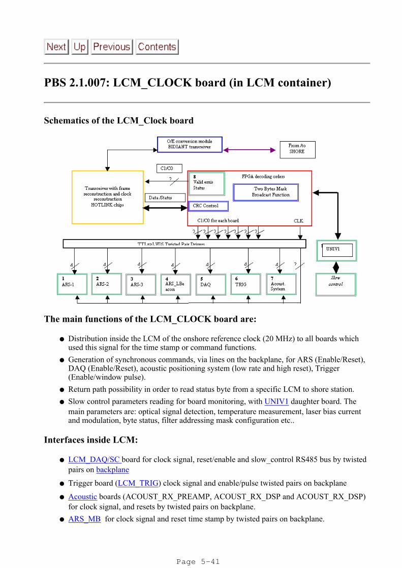
PBS 2.1.007: LCM_CLOCK board (in LCM container)
Schematics of the LCM_Clock board
The main functions of the LCM_CLOCK board are:
Distribution inside the LCM of the onshore reference clock (20 MHz) to all boards whichused this signal for the time stamp or command functions.
Generation of synchronous commands, via lines on the backplane, for ARS (Enable/Reset),DAQ (Enable/Reset), acoustic positioning system (low rate and high reset), Trigger(Enable/window pulse).
Return path possibility in order to read status byte from a specific LCM to shore station.
Slow control parameters reading for board monitoring, with UNIV1 daughter board. Themain parameters are: optical signal detection, temperature measurement, laser bias currentand modulation, byte status, filter addressing mask configuration etc..
Interfaces inside LCM:
LCM_DAQ/SC board for clock signal, reset/enable and slow_control RS485 bus by twistedpairs on backplane
Trigger board (LCM_TRIG) clock signal and enable/pulse twisted pairs on backplane
Acoustic boards (ACOUST_RX_PREAMP, ACOUST_RX_DSP and ACOUST_RX_DSP)for clock signal, and resets by twisted pairs on backplane.
ARS_MB for clock signal and reset time stamp by twisted pairs on backplane.
Page 5-41

ARS LED beacon for clock signal and reset by twisted pair on backplane.
LCM power box for voltage (+5V and +3.3V) by backplane.
LCM optical connection board (LCM_OPTCON), via the BIDIANT transceiver, to themain cable.
Associated Technical Notes:
3 LCM 03 01: Numerical clock distribution for ANTARES (Proposal)
3 LCM 03 02: Clock Board interfaces description
3 LCM 18 02: Clock distribution prototypes tests
Page 5-42

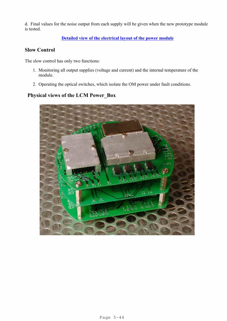
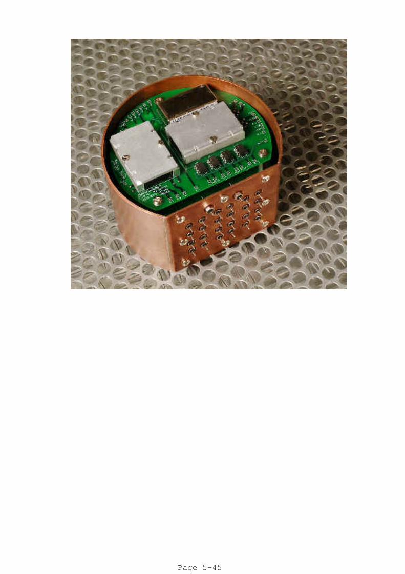
PBS2.1.011: Power Box for LCM and SCM
The LCM power module is contained within a copper housing, which is mounted at one end ofthe power and data bus support assembly. To minimise EMC radiation, all input and outputelectrical connections are made through individual ceramic filters and the housing lid is sealed withberyllium-copper finger strips.
The power module is based upon a VICOR second generation DC to DC converter capable ofoperating with an input voltage range of 290 to 450 V. The first converter generates an internalsupply of 48 V, which is used as the power input to all other converters within the module.
The SCM Power Supply is a copy of the LCM POWER_BOX, although less voltages are used inthe SCM.
Output Specifications
OUTPUT VOLTAGE in Volts MAXIMUM POWER in watts EFFICIENCY in %
48 50 8548
switched outputs3.0
per channel 85
12 3.0 71
5.5 15 70
5.0 50 72
3.3 50 72
2.5 8.0 64
1.8 see below 44
General remarks
a. All outputs (with the exception of the 1.8-volt supply) are fully isolated and there is no commonconnection within the power unit. The 1.8-volt supply is derived from the 2.5-volt output andtherefore the two supplies share the total power (8 watts).
b. The maximum power quoted in the above table does not imply that this level of power isavailable for general use. It is the maximum capability of the individual converters under idealconditions. The available power will depend upon, load distribution, efficiency and mostimportantly the thermal characteristics of the LCM.c. The efficiency quoted, is the overall value from the 400-volt input to the particular output (theefficiency is not constant with load and the above figures are only representative)
Page 5-43
d. Final values for the noise output from each supply will be given when the new prototype moduleis tested.
Detailed view of the electrical layout of the power module
Slow Control
The slow control has only two functions:
Monitoring all output supplies (voltage and current) and the internal temperature of themodule.
1.
Operating the optical switches, which isolate the OM power under fault conditions. 2.
Physical views of the LCM Power_Box
Page 5-44
Page 5-45

PBS 2.1.012: LCM_OPTCON board (in LCM container)
Schematic of the LCM_OPTCON board
The main function of the LCM_OPTCON board is the distribution of all optical fibres orpower wires from the EMC to the LCM_CRATE boards or pass them to next floor.
Each cable (penetrator) has 21 optical monomode fibers and 9 power wires. The LCM_OPTCONboard includes optical connectors and solder contact points for signal distributions.
Optical connectors are OPTOCLIP II connectors from Deutsch company, these connectors hasbeen tested with a power loss insertion lower than 0.1 dB and reproducibility better than 0.05 dB.
For electrical power connection, each LCM_OPTCON board includes PCB wire configurationwhich can be cut or assign for each floor before integration The LCM_OPTCON board is fixed to the upper flange of the LCM container.
Interfaces inside LCM are:
Maximum needs for optical connectors : 27; 30 OPTOCLIP II connectors are available.
Maximum needs for optical fibers with LCM_CRATE boards: 9 for Master LCM and 2
Page 5-46

wires for 400V.
OPTCON prototype board picture
Page 5-47

PBS 2.1.013: UNIV1 board (in LCM, SCM, JB containers)
Schematic diagramme of the UNIV1 board
The main functions of UNIV1 board are:
Main hardware interface between the DAQ/SC board and the setting and reading of theSlow-Control parameters of each board inserted in the containers.
MODBUS protocol in micro-controller with RTU format.
10/12 Analog to Digital converters with 10 bits of precision.
2 Digital to Analog converters with 12 bits of precision.
16 digital pin selectable individual y in IN or OUT state.
1 timer with 16 bit range, second serial bus with buffer transmission and reception.
Interfaces inside LCM, SCM and JB are:
The UNIV1 board is a daughter board which drives all slow-control functions for its mainboard. Hardware adaptation are very small or not necessary.
Page 5-48

Picture of the UNIV1 Board
Associated Technical Notes:
3 LCM 08 01/A : UNIV1 user’s manual
3 LCM 08 02/A: MODBUS reference guide
Page 5-49

PBS 2.1.014: BIDIANT board (in LCM container and SCMcontainer)
Schematic diagramme of the BIDIANT transceiver
The main specifications of the BIDIANT transceiver board are:
Bidirectional distribution of Ethernet or clock distribution using only one optical fibre
Ethernet transmission between LCM slaves and LCM master inside sector, with 1310/1310nm bi-directional capability.
Clock distribution inside sector, with 1310/1550 nm for LCM and 1550/1310nm for SCMcontainers.
Modulation current between 5 to 60 mA with a maximum optical power of –3 dBm for laserdiode.
Laser diode current between 5 to 30 mA with APC power control.
Receiver part with transimpedance and limiting amplifier, with a sensitivity better than –23dBm for 1310/1550 nm and –20 dBm for 1310/1310 nm.
Each transceiver board produce voltages to allow monitoring of the laser diode modulationand bias current. These parameters can be read by the Slow-Control of the UNIV1 board
Page 5-50

Inputs and Outputs are differential in LVPECL format.
Signal detection permits to detect optical power at the receiver.
Interfaces inside LCM:
The BIDIANT transceivers are standard 2x9 pinout, with additional pin for PIN diode biasvoltage (Between 3 to 10 Volts max)
Optical fibres are mounted with OPTOCLIP II connectors.
Picture of the BIDIANT board
Page 5-51

PBS 2.1.015: BIDITRIG board (in LCM container and JBcontainers)
Schematic diagramme of the BIDITRIG transceiver board
This board is a daughter board which is plugged on the LCM_TRIG and JB_TRIG boards. Anexample of a BIDITRIG board implementation can be seen with the picture of the BIDIANT board,the external aspect is similar.
The main functions of the BIDITRIG transceiver board is the electrical/optical conversionbetween TTL pulse of trigger signals L2 and RoR and monomode optical fibres inside the linecable.
Interfaces inside LCM and JB are:
The BIDITRIG daughter board has standard TTL input and output. Power needed +5 V.
Like the BIDIANT daughter board, the BIDITRIG incorporates standard BIDI componentwith pigtail and standard OPTOCLIP II connector on the optical fibres.
Page 5-52
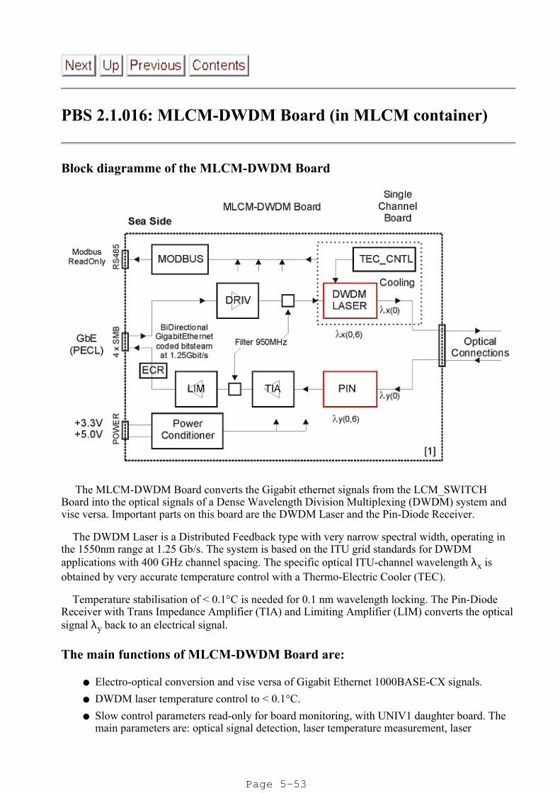
PBS 2.1.016: MLCM-DWDM Board (in MLCM container)
Block diagramme of the MLCM-DWDM Board
The MLCM-DWDM Board converts the Gigabit ethernet signals from the LCM_SWITCHBoard into the optical signals of a Dense Wavelength Division Multiplexing (DWDM) system andvise versa. Important parts on this board are the DWDM Laser and the Pin-Diode Receiver.
The DWDM Laser is a Distributed Feedback type with very narrow spectral width, operating inthe 1550nm range at 1.25 Gb/s. The system is based on the ITU grid standards for DWDMapplications with 400 GHz channel spacing. The specific optical ITU-channel wavelength λx isobtained by very accurate temperature control with a Thermo-Electric Cooler (TEC).
Temperature stabilisation of < 0.1°C is needed for 0.1 nm wavelength locking. The Pin-DiodeReceiver with Trans Impedance Amplifier (TIA) and Limiting Amplifier (LIM) converts the opticalsignal λy back to an electrical signal.
The main functions of MLCM-DWDM Board are:
Electro-optical conversion and vise versa of Gigabit Ethernet 1000BASE-CX signals.
DWDM laser temperature control to < 0.1°C.
Slow control parameters read-only for board monitoring, with UNIV1 daughter board. Themain parameters are: optical signal detection, laser temperature measurement, laser
Page 5-53
wavelength lock, laser bias current and laser modulation current.
Interfaces inside MLCM are:
DAQ/SC Board for Slow-Control, RS485 bus by twisted pairs on LCM backplane.
MLCM_SWITCH board signals via coaxial SMB connectors.
Optical I/O via the EMC to the SCM-DWDM-MUX & DEMUX.
Backplane for supply Voltages: 3.3V and 5.0V.
Associated Technical Notes:
http://www.nikhef.nl/~n05/antares/ETR_Notes/ETR2000-07s.pdf
http://www.nikhef.nl/~n05/antares/ETR_Notes/ETR2000-08s.pdf
Page 5-54
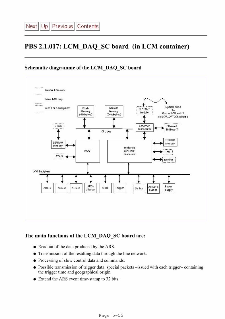
PBS 2.1.017: LCM_DAQ_SC board (in LCM container)
Schematic diagramme of the LCM_DAQ_SC board
The main functions of the LCM_DAQ_SC board are:
Readout of the data produced by the ARS.
Transmission of the resulting data through the line network.
Processing of slow control data and commands.
Possible transmission of trigger data: special packets –issued with each trigger– containingthe trigger time and geographical origin.
Extend the ARS event time-stamp to 32 bits.
Page 5-55

Interfaces inside LCM are:
Clock board (LCM_CLOCK) for clock signal, reset/enable DAQ and Slow-Control overModbus Protocol.
Trigger board (LCM_TRIG) for Readout Request, L2 and L1 trigger signals.
Acoustic boards (ACOUST_RX_PREAMP, ACOUST_RX_DSP and ACOUST_RX_CPU)for slow-control over Modbus Protocol.
ARS motherboards (ARS_MB) for data readout and Slow-control. Both slow-control andreadout are carried by the DAQ FPGA over the ARS protocol.
LCM power box for voltage (+3.3V and +1.8V).
LCM optical connection board (LCM_OPTCON), via the BIDIANT transceiver daughterboard, in order to connect optical signals to the main cable.
Page 5-56

PBS 2.1.018: MLCM_SWITCH board (in Master LCMcontainer)
Schematic of the MLCM_SWITCH board
The main functions of the MLCM_SWITCH board are:
Merge all Ethernet link (100 Mbits/s) coming from the LCM_DAQ_SC boards of a sectorinto a single Ethernet link connected to the DWDM laser board (1 Gbits/s).
Common link characteristics : Ethernet protocol, bi-directional and full-duplex.
Configured at power-up.
Interfaces inside LCM are:
Master LCM BIDIANT board. The BIDIANT transceivers, which receive the link comingfrom all the LCM_DAQ_SC boards of a sector are connected to 4 Fast Ethernet transceivers
Page 5-57

via PECL signals over the backplane.
MLCM_DWDM for the Gigabit link over coaxial cables.
LCM power box for power (+3.3V and +2.5V)
The local LCM_DAQ_SC board
Page 5-58

PBS
PBS2.2: The String Control Module (SCM)
The String Control Module (SCM) contains the electronics concerning the Slow Control, clock,and instruments for acoustic positioning and sea properties.
The SCM container is similar to the LCM container and is located in the Botttom String Socket(BSS). It is coupled to the String Power Module (SPM).
The individual cards in the SCM have dedicated test benches, as is the case for the LCM cards.The tests foreseen for the SCMs are summarised in the page on Integrated SCM test benches.
Components in a SCM
Objects in SCM Description PBSnumber
SCM container Titanium container 1.2.006
SCM_CRATE support of boards and backplane 2.2.001
SCM_BACK1 distributes signals between boards inSCM_CRATE 2.2.002
SCM_WDM1 optical transceiver WDM with clockdistribution 2.2.003
SCM_REP optical transceiver to regenerate clock signal 2.2.004
SCM_CLOCK Clock distribution for SCM 2.2.005
SCM_DWDM Optical transceiver for DWDM function withlaser and receiver part 2.2.006
ACOUST_RXTX_EM Positioning system 2.2.007
ACOUST_RXTX_PREAMP Positioning system 2.2.008
ACOUST_RXTX_DSP2 Positioning system 2.2.009
ACOUST_RXTX_DSP1 Positioning system 2.2.010
ACOUST_CPU Positioning system 2.2.011
ACOUST_POW Positioning system 2.2.012
SCM_OPTCON Optical connections between main cable andSCM_CRATE 2.2.013
Page 5-59

SCM_DWDM_
MUX/DEMUXOptical mux and demux to separate or mixwavelengths from shore or Master LCM 2.2.014
COMPASS_MB Controls and measures tiltmeters, humidity andtemperature sensors (id. LCM) 2.1.003
ARS_MB analog pipeline with ADC conversion fromPMT signal (identical to LCM) 2.1.004
POWER_BOX Converts 400V to needed voltages (id. LCM) 2.1.012
UNIV1 Daughter board plugged on other board forslow control MODBUS interface 2.1.013
LCM_DAQ/SC Data and slow control board which sends andreceives Ethernet Protocol 2.1.017
Page 5-60

SCM Test Bench
SCM Test Bench synoptic
Specifications:
The SCM Test Bench will have to certify the full functionality of the SCM. It will do so bychecking that:
the SCM correctly executes the SC commands
the SCM correctly sends the data locally produced
the SCM correctly receives and internally distributes the CLOCK reference signal. Inaddition, it correctly executes the control instructions that it may receive along the CLOCKconnection
the SCM correctly controls and/or communicates with the devices locally connected: SPM,laser beacon, acoustic transponder, pressure (or CTD) sensor, sound velocimeter
the SCM correctly elaborates the analog signals coming from the Laser Beacon photodiodeand the acoustic transponder
Interfaces to the SCM are:SPM-connector: 400 VDC power from Test Bench power supply to SCM, RS485 twistedpair for SPM slow-control emulation
Page 5-61

JB/SPM-side: DATA/SC and CLOCK fibers (these connections will be made at theOPT_CON level)
String-side: 6 CLOCK fibers (these connections will be made at the OPT_CON level)
Laser beacon connector: 48 V power from SCM, RS485 twisted pair for laser beacon SCemulation, output pulse from SCM for laser drive and analog input from (simulated)photodiode to SCM
Acoustic transponder connector: emulator for analog signal from acoustic transponder
Pressure (or CTD) sensor connector: 48V power from SCM, RS232 serial communicationwith sensor emulator
Sound velocimeter connector: 48V power from SCM, RS232 serial communication withsensor emulator
Backplane: check that the 20 MHz clock from the Clock board is correctly distributed,interface to the internal RS485 MODBUS + others to be defined
Associated Technical Notes
3 SCM 18 01/A: Proposal for a SCM Test Bench (to be released soon)
Page 5-62

PBS2.2.001: SCM_CRATE (in SCM container)
Schematic view of the Inner rack
The design of the SCM_CRATE inner rack is:
The SCM_CRATE inner rack houses the string control module offshore electronics.
It consists of an axial structure that links all the cards and the backplane
Electric and optical cables penetrate the container and are plug in cards.
This structure looks like a cylindrical cage placed inside the SCM container and fixed in thelower bottom end cap by a crown.
Dimensions, technological features:
Effective inner diameter: 155 mm
Effective inner length: 550 mm
The selected material for all part of the inner rack is aluminium 2017. Both inner and outerdiameters must be chamfered
Page 5-63
Interfaces inside SCM are:
16 boards
1 electrical connection board
1 optical connection device
SCM power box for voltage
4 shielding for OEM and thermal conduction
Associated Technical designs:
3 LCM 02 01:Integration LCM
3 LCM 02 03: shielding
3 LCM 02 04: crown 1
3 LCM 02 05: crown 2
3 LCM 02 06: Slides
Page 5-64

PBS 2.2.002: SCM_BACK board (in SCM container)
Schematic diagramme of the SCM_BACK board
The main functions of the SCM_BACK board are:
Distributes inside the SCM container all signals from or to each board inserted inside the SCM_CRATE .
Distributes electrical power: +5V, +3.3V, +2.5V, +1.8V, +12V, +48V and common return,all these power signals come from the POWER_BOX fixed on the SCM_CRATE.
The SCM_BACK interfaces between the optical modules signals and the ARS_MB,POWER_BOX and COMPASS_MB electronics boards.
Each board has a fixed location in order to optimise EMC and parallel development.
Controls the SPM container slow-control function through a second RS485 twisted pair withMODBUS protocol.
Interfaces inside the SCM are:
Each board inserted in the SCM_CRATE is connected to the SCM_BACK with its rearconnector (24, 48, or 96 pins).
1 connector interfaces with the laser beacon PMT (configuration for one line only).
1 connector interfaces with other containers for RS232 and second RS485 serial bus, thisconnector also transmits the test signal for LCM_DAQ/SC board (external test triggersignal). This connector drives also the main RS485 serial bus for all boards inserted insideSCM_CRATE in order to test slow-control without the LCM_DAQ/SC board.
The second RS485 twisted pair controls the SPM slow control function.
The boards inserted inside the SCM_CRATE are:COMPASS_MB, ARS_MB for laser beacon, SCM_DWDM, LCM_DAQ/SC,SCM_WDM,SCM_CLOCK, SCM_REP (2 boards), SCM_ACOUST1 to 6 and
Page 5-65

POWER_BOX.
Associated Technical Notes:
3 SCM 20 01: SCM internal organisation.
Page 5-66

PBS 2.2.003: SCM_WDM (in SCM container)
Schematic diagramme of the SCM_WDM board:
The main specifications of the SCM_WDM module are:
Bi-directional electrical/optical module using WDM (Wavelength Division Multiplexing)concept to send the reference clock and control words from the ON_CLOCK board to all theLCM_CLOCK boards.
Receive status words from a selected LCM_CLOCK board.
The wavelength of the optical signals are 1535 nm from ON_WDM to SCM_WDM and1549 nm for the opposite direction.
The clock signal (converted in electrical PECL format) are sent to the SCM_CLOCK,SCM_REP boards in order to be regenerated and converted to optical signal for each sector.
Slow control parameters reading for board monitoring, with UNIV1 daughter board. Themain parameters are: optical signal reception, switching ON/OFF laser driver, temperaturemeasurement.
Temperature of the laser controlled by Thermoelectric Cooler controller (TEC) DN1220ThermoOptics.
Interfaces to :
SCM_CLOCK board through the Input/Output PECL channels (200 Mbps).
SCM_REP board through the rear connector on SCM_BACK (200 Mbps)
Page 5-67

Technical Notes associated on WEB page:
3 SCM 02 01/B: SCM internal organisation
3 LCM 03 01: Numerical clock distribution for ANTARES (Proposal)
3 LCM 03 02 : Clock Distribution ON_SHORE for ANTARES (Proposal)
3 LCM 08 04: BIDIANT user’s manual
Page 5-68

PBS2.2.004: SCM_REP board (in SCM container)
Schematic of the SCM_REP board
The main specifications of the SCM_REP board are:
Electrical to optical conversion between SCM_WDM board and each sector for clockdistribution function.
Electrical to optical conversion through the BIDIANT daughter boards plugged onSCM_REP board.
The UNIV1 function allows monitoring of the Vbias and Vmonitor voltage of eachBIDIANT daugther boards and one temperature sensor.
Inside each SCM container, we have 2 SCM_REP boards in order to drive clock signals forthe 6 sectors of a line.
Interfaces inside SCM are:
Clock electrical signal goes from SCM_WDM to SCM_CLOCK and SCM_REP (first) andSCM_REP (second) in serial topology via a PECL twisted pair.
DAQ board for clock signal, reset/enable and slow_control RS485 bus by twisted pairs onbackplane
SCM_WDM board with twisted pairs PECL ( clock signal) on backplane SCM_BACK.
POWER_BOX for voltage (+5V and +3.3V) by backplane
Page 5-69

Associated Technical Notes:
3 LCM 03 01: Numerical clock distribution for ANTARES (Proposal)
3 LCM 03 02: Clock Board interfaces description
3 LCM 18 02: Clock distribution prototypes tests
3 SCM02 01: SCM internal organisation
Page 5-70
PBS2.2.005: SCM_CLOCK board (in SCM container)
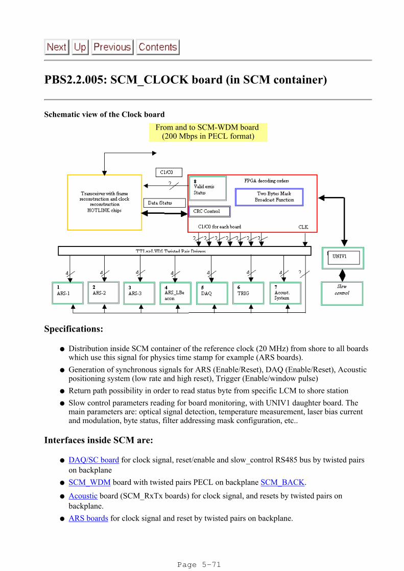
Schematic view of the Clock board From and to SCM-WDM board
(200 Mbps in PECL format)
Specifications:
Distribution inside SCM container of the reference clock (20 MHz) from shore to all boardswhich use this signal for physics time stamp for example (ARS boards).
Generation of synchronous signals for ARS (Enable/Reset), DAQ (Enable/Reset), Acousticpositioning system (low rate and high reset), Trigger (Enable/window pulse)
Return path possibility in order to read status byte from specific LCM to shore station
Slow control parameters reading for board monitoring, with UNIV1 daughter board. Themain parameters are: optical signal detection, temperature measurement, laser bias currentand modulation, byte status, filter addressing mask configuration, etc..
Interfaces inside SCM are:
DAQ/SC board for clock signal, reset/enable and slow_control RS485 bus by twisted pairson backplane
SCM_WDM board with twisted pairs PECL on backplane SCM_BACK.
Acoustic board (SCM_RxTx boards) for clock signal, and resets by twisted pairs onbackplane.
ARS boards for clock signal and reset by twisted pairs on backplane.
Page 5-71

ARS laser beacon for clock signal and reset by twisted pair on backplane.
POWER_BOX for voltage (+5 V and +3.3 V) by backplane
Technical Notes:
3 LCM 03 01: Numerical clock distribution for ANTARES (Proposal)
3 LCM 03 02: Clock Board interfaces description
3 LCM 18 02: Clock distribution prototypes tests
3 SCM02 01: SCM internal organisation
Page 5-72

PBS 2.2.006: SCM-DWDM Board (in SCM container)
Schematic diagramme of the SCM-DWDM Board:
The SCM-DWDM Board converts the Fast Ethernet signals from the DAC/SC Board into theoptical signals of a Dense Wavelength Division Multiplexing (DWDM) system and vise versa.Important parts on this board are the DWDM Laser and the Pin-Diode Receiver. The DWDM Laseris a Distributed Feedback type with very narrow spectral width, operating in the 1550nm range at1.25 Gb/s. The system is based on the ITU grid standards for DWDM applications with 400 GHzchannel spacing.The specific optical ITU-channel wavelength λx is obtained by very accuratetemperature control with a Thermo-Electric Cooler (TEC). Temperature stabilisation of < 0.1°C isneeded for 0.1nm wavelength locking. The Pin-Diode Receiver with Trans Impedance Amplifier(TIA) and Limiting Amplifier (LIM) converts the optical signal λy back to an electrical signal.
The main specifications of SCM-DWDM Board are:
Electro-Optical conversion and vice versa of Fast Ethernet 100BASE-TX signals.
DWDM Laser temperature control to < 0.1°C.
Slow control parameters Read-Only for board monitoring, with UNIV1 daughter board. Themain parameters are: optical signal detection, laser temperature measurement, laserwavelength lock, laser bias current and laser modulation current.
Interfaces inside SCM are:
DAQ/SC Board for Slow-Control, RS485 bus by twisted pairs on SCM backplane.
Page 5-73

DAQ/SC Board Fast Ethernet signals via coaxial SMB connectors.
Optical I/O to the SCM-DWDM-MUX & DEMUX
Backplane for Supply Voltages; 3.3V and 5.0V.
Associated Technical Notes:
http://www.nikhef.nl/~n05/antares/ETR_Notes/ETR2000-07s.pdf
http://www.nikhef.nl/~n05/antares/ETR_Notes/ETR2000-08s.pdf
Page 5-74

PBS 2.2.014: SCM-DWDM-MUX & DEMUX (in SCMcontainer)
SCM-DWDM-MUX & DEMUX schematic:
The SCM-DWDM-MUX & DEMUX is a passive optical circuit inside the SCM container.Optical signals to and from the MLCMs are split/combined with Dense Wavelength DivisionMultiplexers and Demultiplexers. The optical signals; λx(0:6), 6 wavelengths from the MLCMs forDAQ and 1 for SCM-SC, are multiplexed with a DWDM Multiplexer into a single mono modefiber. The optical signals from the JB (Shore Station), λy(0:6) are demultiplexed with aDWDM-Demultiplexer into 7 output fibers. Two sets of 6 wavelengths are used for DAQ -GigabitEthernet- and a 7th set is used for SCM-SC (Fast -100Mb- Ethernet).
The DWDM Multiplexer and DWDM Demultiplexer use thin film interference filters, the opticalpath is epoxy free. The ITU wavelength grid used for these DWDMs is 400 GHz (~3.2 nm). TheDWDM channels have a minimum bandwidth of 0.8 nm.
The main functions of SCM-DWDM-MUX & DEMUX are:
Multiplexing and demultiplexing of optical signals. Optical signals are ITU defined channelwavelengths in the 1550 nm band on a 400 GHz grid. All optical parts are passive.
Page 5-75

Interfaces inside SCM are:
Optical I/O to E/O-O/E Board for Slow-Control of the SCM
Optical I/O from the MLCMs and to the JB.
Associated Technical Notes:
http://www.nikhef.nl/~n05/antares/ETR_Notes/ETR2000-07s.pdf
http://www.nikhef.nl/~n05/antares/ETR_Notes/ETR2000-08s.pdf
Page 5-76

Electrical Power System PBS list
PBS 2.3 : The String Power Module (SPM)
Schematic view of the SPM
The String Power Module (SPM) is fed by the 1000 Vac of the Junction Box. It converts the 1000Vac to 400 Vdc for use in the LCMs of a string. It also provides 48 Vdc for the control systems ofthe SPM and SCM.
The SPM consists of three pairs of ring core transformers, each pair feeds two sectors and eachhas a fuse to prevent shorting of the 1000 V by a single transformer. Each output has a Solid StateRelay (SSR) which isolates a sector in the case of failure inside a LCM. A Power Factor Corrector(PFC) circuit provides an almost resistive load to the transformer, giving high efficiencyrectification and low noise.
All output currents, voltages and the supply temperatures are monitored by the Slow ControlUNIV board. All outputs can be switched on/off by remote control. Over-temperature andover-current situations are handled locally.
Page 5-77

The thermal cooling of the SPM is understudy, the preferred solution is that adopted for the LCMcontainer, in which copper fingers connect to the walls of the SPM container. Further details can befound in the internal note on SPM.
The components used satisfy military specifications, the expected MTBF is of the order of 50years.
Specifications:
Input
Voltage to activate the localslow control 680-1000 V
Voltage to deliver 6* output 720-1000 Vfrequency range 48-55 Hzpower factor >0.97Cos phi >0.95Nominal power 1300 W
Output: 6* 380 Vdc
voltage variations <5%ripple <10%ttnoise <1%ttnominal power 180 Wattsmaximum power 200 Wattsoverload protection fuse
Output: 1*48 Vdc
voltage variations <5%ripple <10%ttnoise <1%ttnominal power 50 Wattsmaximum power 60 Wattsoverload protection fuse
Monitoring
1* ac input voltage6*dc output voltages6*dc output currents1*ac leakage current to container 0-10mA1*dc-leakage current to container 0-10mA
Page 5-78

InterfacesJB via an Interconnecting Link cable
SCM
Objects in SPM Description PBSnumber
SPM_CONTAINER contains all the items below 1.2.007
SPM_CRATE support of boards and backplane 2.3.001
SPM_BACK1 distributes signals between boards inSPM_CRATE 2.3.002
SPM_CONNECT1 connections inside SPM 2.3.003
SPM_CONNECT2 connections inside SPM 2.3.004
SPM_CONT1 controls power distribution 2.3.005
SPM_CONT2 controls power distribution 2.3.006
SPM_CONT3 controls power distribution 2.3.007
SPM_CONT4 controls power distribution 2.3.008
SPM_LV Produces low voltage 2.3.009
SPM_TRANS1 transformer for HV AC 2.3.010
SPM_FILT1 electrical filter for power conversion 2.3.011
SPM_REGUL Voltage regulator 2.3.012
SPM_DC/DC DC/DC conversion 2.3.013
SPM_FILT2 Electrical filter on output 2.3.014
SPM_HEAT1 Heat dissipator 2.3.015
UNIV1 Daughter board plugged on other board forslow control MODBUS interface 2.1.013
List of References
Power section in Chapter 7
SPM technical note, to be released soon.
Page 5-79
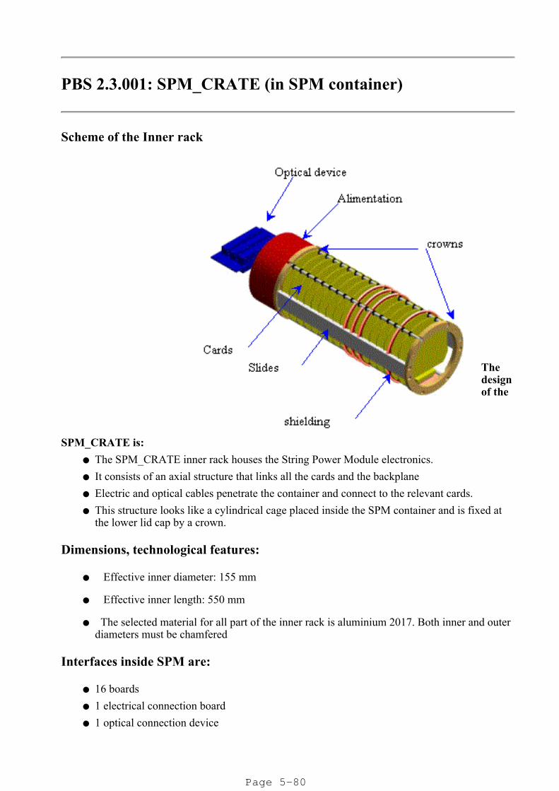
PBS 2.3.001: SPM_CRATE (in SPM container)
Scheme of the Inner rack
Thedesignof the
SPM_CRATE is:The SPM_CRATE inner rack houses the String Power Module electronics.
It consists of an axial structure that links all the cards and the backplane
Electric and optical cables penetrate the container and connect to the relevant cards.
This structure looks like a cylindrical cage placed inside the SPM container and is fixed atthe lower lid cap by a crown.
Dimensions, technological features:
Effective inner diameter: 155 mm
Effective inner length: 550 mm
The selected material for all part of the inner rack is aluminium 2017. Both inner and outerdiameters must be chamfered
Interfaces inside SPM are:
16 boards
1 electrical connection board
1 optical connection device
Page 5-80

LCM power box for voltage
4 shielding boards for OEM and thermal cooling
Associated Technical drawings at:http://antares.in2p3.fr/internal/deci-km2/tableaux/LCM.htm
3 LCM 02 01:Integration LCM
3 LCM 02 03: shielding
3 LCM 02 04: crown 1
3 LCM 02 05: crown 2
3 LCM 02 06: Slides
15/02/2001 M.Jaquet/P.Lagier
Page 5-81

List of subsystems PBS list Mechanics Electronics Electrical Power
The Junction Box list of objects
The Junction Box (JB) is the heart of the ANTARES detector. It receives Power from theonshore Power Hut via the Main Electro-Optical Cable (MEOC) and distributes it to the strings viathe Interconnecting Links (IL). Data, Clock, Trigger and Control signals also transit via the JBthrough the same cables.
Components are separated into mechanics, electronics and power aspects and each of theseaspects is described separately in the corresponding chapter.
Since it is is the first detector system we build, to be installed in the sea, it has the first PBSnumber. The associated PBS numbering has been fixed by the collaboration organisationalstructure (starting with 1 for mechanics, 2 for electronics and 6 for power). A list of the componentscan be found below.
PBS 1. 1 Junction Box: mechanics part
PBS1.1.1 JB FramePBS1.1.2 JB_Container
PBS1.1.2.001 JB Vessel 2 Ti hemispheres and 1cylind. spacer
PBS1.1.2.002 JB Diaphragm separates the transformer tothe electronic volumes
PBS1.1.2.003 Feed-throughs transmit power anddiagnostic (7)
PBS1.1.2.004 PRE-JB holds penetrator forconnection to EO cable
PBS1.1.2.005 JB O-ring PBS1.1.2.006 Balancing devicePBS1.1.3 Acoustic Beacon support
PBS8.1.5 LBL Acoustic Beacon gives the position of theframe
PBS 2.4 Junction Box clock distribution and trigger construction
PBS2.4.001 JB_ELECBOX contains electronics boards
PBS2.4.002 JB_SPLIT1 passive splitters for clock distribution
PBS2.4.003 JB_TRIG1 RoR signal construction
PBS2.1.013 UNIV1 Daughter board plugged on other board forslow control MODBUS interface
PBS6.4: Junction Box (Power part)
PBS6.4.1 Penetrators and bulkhead receptacles
Page 5-82

PBS6.4.2 Power components PBS6.4.3 Power Remote diagnostic PBS6.4.4 Very Low Voltage Power Supply PBS6.4.5 Cabling and Connections PBS6.4.6 Sensors PBS6.4.7 Remote Control
links to TDR
Junction Box Mechanical Description
Electronics Power Distribution
Electrical Power system
Page 5-83

PBS2.4.001: JB ELECBOX
Schematic views of the JB ELECBOX
Requirements
The main mechanical function is to support all the electronics box.
An assembly has been performed
All presently defined parts fit in
Connection and accessibility tests : to be done
Assembly on JB container tests : will be done in CPPM
Listing components in electronics box
16 out switch 105x116x130
7 out ctl 102x33x95
1 out sensor60x60x60
1 clock + ROR 320x150x126
1 control module 320x150x126
1 low volt 256x131x100
1 EOC terminal110x170x150
1 electrode Terminal110x170x50
1 current meas 250x200x65
1 relay 200x135x63
2 relays 130x90x60
Dimensions, technological features:Support interface diameter: 800 mm
Total height: 373 mm
Page 5-84

Technical design
3 BJO-04-01 A Ensemble interne JB
Page 5-85

PBS 2.4.002: JB-SPLIT board (in Junction Box container)
Schematic diagramme of the JB-SPLIT board:
The main specifications of the JB_SPLIT board are:
Distribute to all lines of the detector optical clock signal with a division (splitting function)from 2 fibres to 16 outputs fibres.
Two optical fibres come from shore in order to have a redundancy capability for betterreliability.
The reference of this optical component from E-TEK company is TWSCBE00PH215, wecan find more details about this component in E-TEK company web page: www.e-tek.com.
Interfaces inside JB are:
Inputs and outputs optical fibres are connected to optical fibres which come from MEOCand each JB to the Interconnecting links by an optical connector from Deutsch companyOPTOCLIP II standard.
No electrical power needs, passive component.
Page 5-86

Picture of this component, inserted in crate for tests and measurement
Technical Notes
3 LCM 03 01: Numerical clock distribution for ANTARES (Proposal)
3 LCM 18 02: Clock distribution prototypes tests
Page 5-87

PBS2.4.003: JB-TRIG board (JB container)
Schematic of the JB-TRIG transceiver board:
The main specifications of the JB-TRIG transceiver board are:
Concentrate all L2 signals from each string of the detector and return the RoR signal to alllines.
This OR function is built with an optical splitter with 16 channels inputs and 2 channelsoutputs (2 for redundancy).
The optical OR signal (between all L2 signals) is converted to an electrical signal which isreturned after an O/E/O conversion in a BIDITRIG board. A second BIDITRIG board can beused if the first fails.
A spare channel optical channel is sent to shore in order to monitor the RoR signals of thedetector. Two fibres are reserved inside the MEOC for this function.
A pair of optical fibres are reserved to allowing sending of a 'fake' L2 signal from shore.
Page 5-88

Interfaces inside LCM and JB are:
The BIDITRIG daughter board has standard TTL input and output with +5V powervoltage.The BIDITRIG incorporates standard BIDI component with pigtail and standardOPTOCLIP II connector on optical fibre.
The reference of this optical splitter 2 to 16 from E-TEK company is TWSCBE00PH215,more details about this component can be found in E-TEK company web page:www.e-tek.com
Power needs for this JB-TRIG board is produced internally by a DC/DC converter withstandard 24 Volts input produced by the power box in the Junction Box.
Page 5-89

PBS2.5: On shore Clock objects
The clock is produced on shore and sent to all the storeys. The function is described in therelevant Electronics section about the clock distribution.
Object in Onshore CLOCKcontainer Description PBS
number
ON_CRATE1 Electronics crate 2.5.001
ON-GPS GPS receiver producing reference signal forclock distribution 2.5.002
ON_CLOCK Coding /decoding orders for clockdistribution 2.5.003
ON_WDM Optical transceiver for clock distribution 2.5.004
ON_SYNCPC1 PC board 2.5.005
ON_PCIO digital interface for ON_CLOCK board 2.5.006
Page 5-90
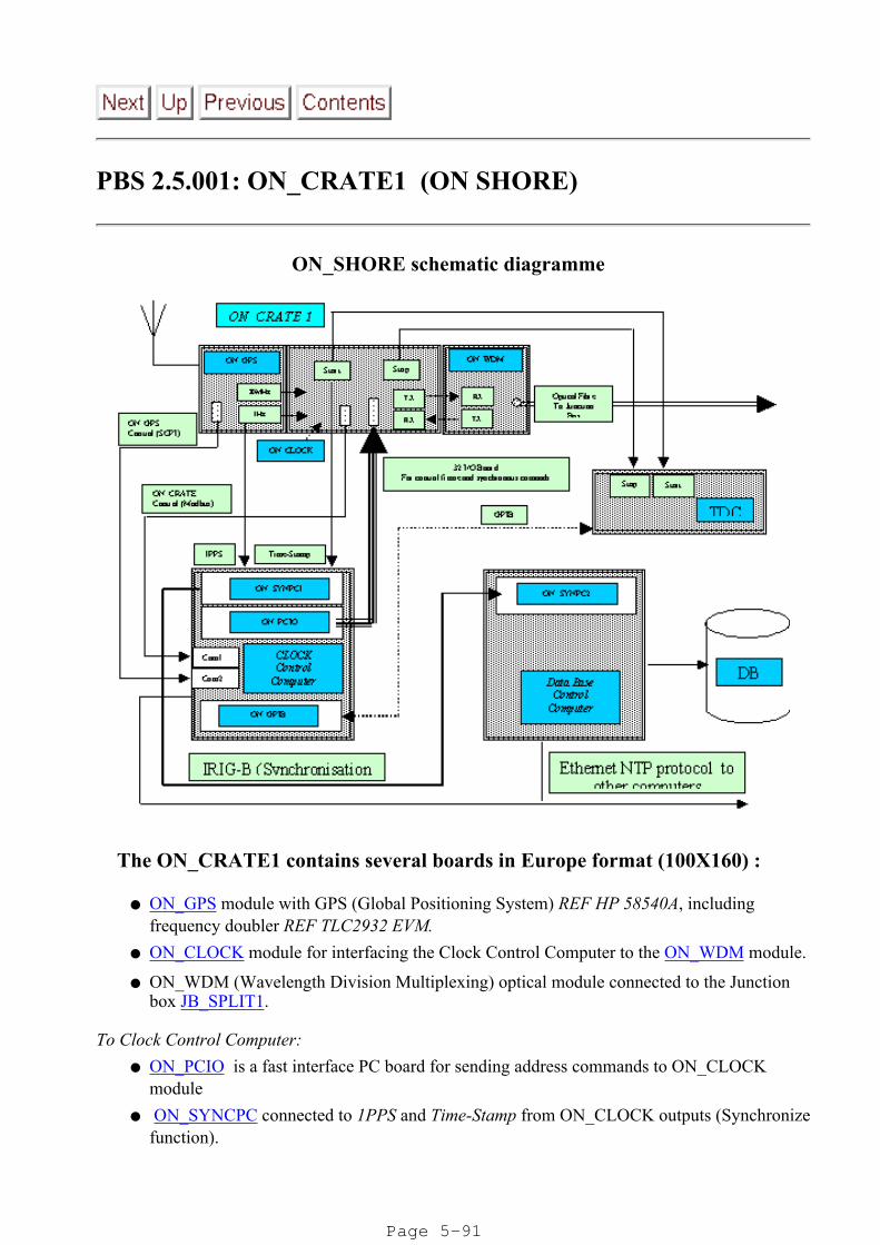
PBS 2.5.001: ON_CRATE1 (ON SHORE)
ON_SHORE schematic diagramme
The ON_CRATE1 contains several boards in Europe format (100X160) :
ON_GPS module with GPS (Global Positioning System) REF HP 58540A, includingfrequency doubler REF TLC2932 EVM.
ON_CLOCK module for interfacing the Clock Control Computer to the ON_WDM module.
ON_WDM (Wavelength Division Multiplexing) optical module connected to the Junctionbox JB_SPLIT1.
To Clock Control Computer: ON_PCIO is a fast interface PC board for sending address commands to ON_CLOCKmodule
ON_SYNCPC connected to 1PPS and Time-Stamp from ON_CLOCK outputs (Synchronizefunction).
Page 5-91

Com1 using a Slow Control MODBUS protocol for ON_CRATE1 Monitoring function.
Com2 using SCPI protocol for ON_GPS monitoring function.
To TDC (Time to digital convert): Start/stop: Outputs TTL pulse for propagation time measurement between the onshorestation and all offshore modules.
Technical Notes:
3 LCM 03 01: Numerical clock distribution for ANTARES (Proposal)
3 LCM 03 02 : Clock Distribution ON_SHORE for ANTARES (Proposal)
Page 5-92

PBS 2.5.002: ON_GPS (ON SHORE)
ON_GPS (Global Positioning System)
The main specifications of the ON_GPS module are:
Provide a high accuracy clock 20 MHz (+/- 50ps jitter) to the offshore electronic boards.
Provide the absolute date and time in coincidence to the UTC (Universal CoordinatedTime).
Interfaces:
The 20 MHz square signal is provided by a frequency doubler (TLC2932 EVM) from the 10MHz GPS clock. This reference clock is connected to the input clock ON_CLOCK board.
The 1 PPS output provides to the PC_CLOCK a synchronized signal in coincidence to theUTC.
A RS232 interface allows keeping date, time and GPS monitoring by using SCPI protocol.
List of References
3 LCM 03 01: Numerical clock distribution for ANTARES (Proposal)
3 LCM 03 02 : Clock Distribution ON_SHORE for ANTARES (Proposal)
Page 5-93

PBS 2.5.003: ON_CLOCK (onshore)
Schematic view of ON_CLOCK board
The main specifications of the ON_CLOCK module are:
Shape and send control words from PC_CLOCK to the WDM optical module at 200 Mbpsspeed.
In the receive mode, shape the status frame from the offshore modules.
Provide START and STOP signals corresponding to the sending and receiving frames forthe propagation time measurement.
Provide a control signal for the time-stamp function.
Interfaces to :
ON_WDM connected by twisted pairs in PECL logic for the send mode and receive mode.
ON_PCIO PC board connected it by large cable (32 bits) for the sending control words.
TDC (Time to Digital Convert) from start and stop output signal .
Page 5-94

ON_SYNCPC1 board to provide a heartbeat rate needed for the PC onshoresynchronization.
Slow Control for board monitoring.
List of References
3 LCM 03 01: Numerical clock distribution for ANTARES (Proposal)
3 LCM 03 02 : Clock Distribution ON_SHORE for ANTARES (Proposal)
Page 5-95

PBS 2.5.004: ON_WDM (onshore)
Schematic diagramme of the ON_WDM board:
The main specifications of the ON_WDM module are:
Bi-directional electrical/optical module using WDM (Wavelength Division Multiplexing)concept to send the reference clock and control words from ON_CLOCK to allLCM_CLOCK boards. Receive status words from selected LCM_CLOCK board.
The wavelength of the optical signals are 1535 nm from ON_WDM to SCM_WDM1 and1549 nm for the opposite direction.
Slow control parameters reading for board monitoring, with UNIV1 daughter board. Themain parameters are: Optical signal reception, Switching ON/OFF laser driver, Temperaturemeasurement.
The temperature of the laser is controlled byThermoelectric Cooler controller (TEC) DN1220 ThermoOptics.
Interfaces to :
ON_CLOCK board through the Input/Output PECL channels (200 Mbits/s).
SCM_WDM1 boards through the shore cable Optical fibre (50 Km).
ON_CRATE1 for the Slow control functions by RS485.
List of References
Page 5-96

3 LCM 03 01: Numerical clock distribution for ANTARES (Proposal)
3 LCM 03 02 : Clock Distribution ON_SHORE for ANTARES (Proposal)
Page 5-97

PBS 2.5.005: ON_SYNCPC1 (ON SHORE / PC- CLOCK)
PCI-SYNCCLOCK32 BRANDYWINE board:
The main specifications of the ON_SYNCPC1 module are:
Provide absolute Date and Time in relationship with the UTC signal from the GPS.
Provide Time-stamp of the control word sending with 100ns precision time.
Provide IRIG B protocol generator allowing absolute Date and Time sending to othercomputer.
Interfaces to:
GPS/UTC (Universal coordinated Time) output for synchronous time function
ON_CLOCK board from Time-stamp output to the PC-SYNC Event time tags input.
IRIG-B generator output to reception of IRIG-B PC Board with another computer.
List of References
3 LCM 03 01: Numerical clock distribution for ANTARES (Proposal)
3 LCM 03 02 : Clock Distribution ON_SHORE for ANTARES (Proposal)
http://www.brandywinecomm.com
Page 5-98
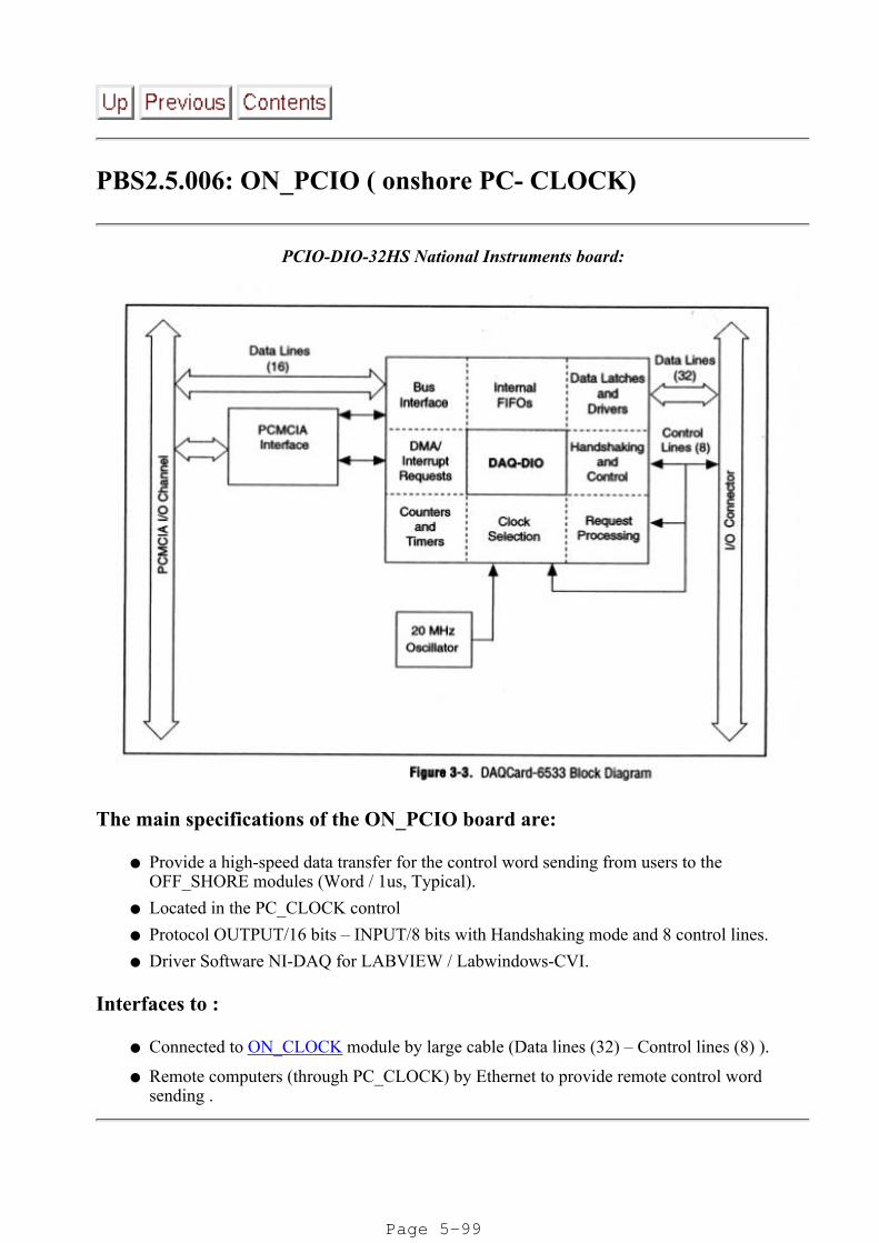
PBS2.5.006: ON_PCIO ( onshore PC- CLOCK)
PCIO-DIO-32HS National Instruments board:
The main specifications of the ON_PCIO board are:
Provide a high-speed data transfer for the control word sending from users to theOFF_SHORE modules (Word / 1us, Typical).
Located in the PC_CLOCK control
Protocol OUTPUT/16 bits – INPUT/8 bits with Handshaking mode and 8 control lines.
Driver Software NI-DAQ for LABVIEW / Labwindows-CVI.
Interfaces to :
Connected to ON_CLOCK module by large cable (Data lines (32) – Control lines (8) ).
Remote computers (through PC_CLOCK) by Ethernet to provide remote control wordsending .
Page 5-99

List of References
3 LCM 03 01: Numerical clock distribution for ANTARES (Proposal)
http://www.ni.com
Page 5-100